include proprietary or classifled ... - auburn university
TRANSCRIPT

Analysis and Correction of Three-Dimensional Proximity Effect in Binary
E-beam Nano-Lithography
Except where reference is made to the work of others, the work described in this thesis ismy own or was done in collaboration with my advisory committee. This thesis does not
include proprietary or classified information.
Kasi Lakshman Karthi, Anbumony
Certificate of Approval:
Stanley J. ReevesProfessorElectrical and Computer Engineering
Soo-Young Lee, ChairProfessorElectrical and Computer Engineering
Ramesh RamadossAssistant ProfessorElectrical and Computer Engineering
Joe F. PittmanInterim DeanGraduate School

Analysis and Correction of Three-Dimensional Proximity Effect in Binary
E-beam Nano-Lithography
Kasi Lakshman Karthi, Anbumony
A Thesis
Submitted to
the Graduate Faculty of
Auburn University
in Partial Fulfillment of the
Requirements for the
Degree of
Master of Science
Auburn, AlabamaMay 10, 2007

Analysis and Correction of Three-Dimensional Proximity Effect in Binary
E-beam Nano-Lithography
Kasi Lakshman Karthi, Anbumony
Permission is granted to Auburn University to make copies of this thesis at itsdiscretion, upon the request of individuals or institutions and at
their expense. The author reserves all publication rights.
Signature of Author
Date of Graduation
iii

Vita
Kasi Lakshman Karthi, Anbumony was born in Nagercoil, Kanyakumari District, Tamil
Nadu, India on November 26, 1982. He entered the Hindustan College of Engineering, Uni-
versity of Madras in 2000 and received a B.E. with honors in Electronics and Communication
Engineering in 2004. In August 2004, he started his graduate career in Auburn University,
completing his M.S. in Electrical and Computer Engineering in December 2006.
iv
Thesis Abstract
Analysis and Correction of Three-Dimensional Proximity Effect in Binary
E-beam Nano-Lithography
Kasi Lakshman Karthi, Anbumony
Master of Science, May 10, 2007(B.E., University of Madras in India, 2004)
101 Typed Pages
Directed by Soo-Young Lee
One of the fundamental problems in transferring a circuit pattern onto a substrate using
electron beam lithography is the proximity effect, which is due to electron scattering in the
resist and results in the “non-ideal” distribution of exposure (energy deposited in the resist)
leading to the blurring of the written circuit pattern. For high-density circuit patterns with
fine features of nanometer scale, the proximity effect can become so severe that features
may merge if not corrected for the effect. All of the previous proximity effect correction
schemes used a two-dimensional (2-D) exposure model for proximity effect correction by
ignoring or averaging the variation of exposure along the depth dimension in the resist. In
this thesis, the three-dimensional (3-D) proximity effect correction for binary lithography is
addressed with emphasis on sidewall shape. The objective of 3-D correction is to control
electron beam dose distribution within each circuit feature using a 3-D point spread function
(PSF) in order to achieve a certain desired remaining resist profile after development.
As the first step towards developing 3-D proximity effect correction schemes, two pro-
totype versions, 3-D iso-exposure contour correction and 3-D resist profile correction, have
v

been implemented in this thesis. The main purpose of these prototype implementation is to
demonstrate the efficiency of real 3-D correction and, therefore, the iso-exposure contours
and resist profiles of certain cross-sections in one direction only are considered in these
versions. The 3-D resist profile correction leads to more realistic results in general since it
takes the resist development process into account.
Through computer simulations, the 3-D proximity effect and performance of the 3-D
correction methods have been analyzed for simple patterns such as a single and three-line
patterns.
vi

Acknowledgments
I would like to thank my advisor Dr. Soo-Young Lee for all his support, detailed
guidance and many helpful suggestions throughout the entire development of PYRAMID
for three-dimensional lithography without which this thesis would not have been possible.
I would also like to thank the other members of my committee, Dr. Stanley J. Reeves and
Dr. Ramesh Ramadoss for their help and support. Thanks are also due to the National
Science Foundation followed by Seagate Technology for funding this research and to Auburn
University and Department of ECE for their financial support. I would also like to thank
Dr. Fei Hu for helping me get familiar with the previous PYRAMID programs. Last but
not least, I would like to thank my family, my friends and all other people who have given
me help during my M.S. study.
To my loved family members and heavenly abodes, without whose support I would not
be able to be where I am now.
vii

Style manual or journal used Bibliography conforms to those of the transactions of
the Institute of Electrical and Electronics Engineers
Computer software used LATEX typesetting language with aums style file developed
by the Auburn University Department of Mathematics
viii

Table of Contents
List of Figures xi
List of Tables xvii
1 Introduction 11.1 Previous Work . . . . . . . . . . . . . . . . . . . . . . . . . . . . . . . . . . 21.2 Motivation and Objectives . . . . . . . . . . . . . . . . . . . . . . . . . . . . 31.3 Organization of the Thesis . . . . . . . . . . . . . . . . . . . . . . . . . . . . 4
2 Three-Dimensional Models 52.1 Electron Beam Lithography . . . . . . . . . . . . . . . . . . . . . . . . . . . 5
2.1.1 Proximity Effect Correction . . . . . . . . . . . . . . . . . . . . . . . 52.1.2 Point Spread Function . . . . . . . . . . . . . . . . . . . . . . . . . . 6
2.2 2-D Exposure Model . . . . . . . . . . . . . . . . . . . . . . . . . . . . . . . 72.3 3-D Exposure Model . . . . . . . . . . . . . . . . . . . . . . . . . . . . . . . 82.4 Resist Development Model . . . . . . . . . . . . . . . . . . . . . . . . . . . . 10
2.4.1 Model . . . . . . . . . . . . . . . . . . . . . . . . . . . . . . . . . . . 112.4.2 Simulation (Cell Removal Model) . . . . . . . . . . . . . . . . . . . . 11
3 Analysis of Three-Dimensional Proximity Effect in E-Beam Lithogra-phy 163.1 Intra-Proximity Effect . . . . . . . . . . . . . . . . . . . . . . . . . . . . . . 163.2 Inter-Proximity Effect . . . . . . . . . . . . . . . . . . . . . . . . . . . . . . 183.3 Simulation Results and Discussion . . . . . . . . . . . . . . . . . . . . . . . 19
3.3.1 Iso-Exposure Contours . . . . . . . . . . . . . . . . . . . . . . . . . . 203.3.2 Intra-Proximity Effect . . . . . . . . . . . . . . . . . . . . . . . . . . 213.3.3 Inter-Proximity Effect . . . . . . . . . . . . . . . . . . . . . . . . . . 253.3.4 Exposure . . . . . . . . . . . . . . . . . . . . . . . . . . . . . . . . . 293.3.5 Resist Development Profile . . . . . . . . . . . . . . . . . . . . . . . 30
4 Three-Dimensional Correction Approaches 344.1 PYRAMID Correction Procedure . . . . . . . . . . . . . . . . . . . . . . . . 344.2 3-D Iso-Exposure Contour Correction . . . . . . . . . . . . . . . . . . . . . 364.3 Resist Profile Correction . . . . . . . . . . . . . . . . . . . . . . . . . . . . . 41
4.3.1 Model . . . . . . . . . . . . . . . . . . . . . . . . . . . . . . . . . . . 414.3.2 Correction . . . . . . . . . . . . . . . . . . . . . . . . . . . . . . . . . 424.3.3 Multi-layer Multi-region Correction . . . . . . . . . . . . . . . . . . . 45
ix

5 Comparison of Correction Schemes 495.1 Error Definition . . . . . . . . . . . . . . . . . . . . . . . . . . . . . . . . . . 495.2 Correction Schemes . . . . . . . . . . . . . . . . . . . . . . . . . . . . . . . . 515.3 Simulation Results and Discussion . . . . . . . . . . . . . . . . . . . . . . . 51
5.3.1 Vertical Sidewall . . . . . . . . . . . . . . . . . . . . . . . . . . . . . 515.3.2 Overcut Sidewall . . . . . . . . . . . . . . . . . . . . . . . . . . . . . 595.3.3 Undercut Sidewall . . . . . . . . . . . . . . . . . . . . . . . . . . . . 655.3.4 Three-line pattern . . . . . . . . . . . . . . . . . . . . . . . . . . . . 74
6 Concluding Remarks and Future Study 76
A Implementation 78A.1 Unit of exposure . . . . . . . . . . . . . . . . . . . . . . . . . . . . . . . . . 78A.2 Resist Development Modeling Constants . . . . . . . . . . . . . . . . . . . . 78
Bibliography 80
x

List of Figures
2.1 Illustration of a binary lithographic process. . . . . . . . . . . . . . . . . . . 6
2.2 A PSF for the substrate system of 500 nm PMMA on Si with the beamenergy of 50 keV: (a) the top, middle and bottom layers, and (b) all layers . 7
2.3 A 2-D PSF for the substrate system comprising 500 nm PMMA on Si withthe beam energy of 50 keV. . . . . . . . . . . . . . . . . . . . . . . . . . . . 8
2.4 A substrate system model consisting of a substrate and resist of thickness T .Substrate system is assumed to be spatially homogeneous, i.e., the substratecomposition and the resist thickness (T ) do not change with location. Z-axisrepresents the resist depth. . . . . . . . . . . . . . . . . . . . . . . . . . . . 9
2.5 Nonlinear relationship: (a) rate vs. 3-D exposure and (b) 3-D exposure vs.depth. Exposure is normalized by 1010. For a feature of width L: 50 nm,Dose: 200 µC/cm2, 1000 nm PMMA on Si, 50 keV. . . . . . . . . . . . . . 10
2.6 Cell removal algorithm: 2-D cell removal model. . . . . . . . . . . . . . . . . 13
2.7 Status of cell (i, j) where Case 1: (a),(b) and (c) single side development;Case 2: (d),(e), and (f) double side development; Case 3: (g) triple side devel-opment. Unshaded are the developed cells and shaded are the undevelopedcells. Arrow heads point in the direction of developer flow. . . . . . . . . . . 14
3.1 Cross-section of the remaining resist for a line feature: (a) overcut (δw > 0)and (b) undercut (δw < 0). . . . . . . . . . . . . . . . . . . . . . . . . . . . 17
3.2 Variation of line width due to inter-proximity effect among multiple lineswhen δwi > 0 for all i. . . . . . . . . . . . . . . . . . . . . . . . . . . . . . . 18
3.3 Comparison of the remaining resist profile (ra(x)) with the desired one (rd(x)of “straight vertical sidewalls”) where the difference between the two profilesis shown as the shaded areas. The ratio of line to space (L:S) is 1:1. . . . . 18
3.4 Cross-sections (X-Z plane) of exposure distribution in the resist when a rect-angular feature with the width (L) of 50 nm is exposed with the dose of 200µC/cm2: (a) grayscale image and (b) iso-exposure contours. The substratesystem consists of 500 nm PMMA on Si and the electron beam energy is 50keV. The unit of exposure is µC/cm2. . . . . . . . . . . . . . . . . . . . . . 20
xi
3.5 Dependency of line width (after development) on resist depth (top, middleand bottom layers) for the substrate system of PMMA on Si and 50 keVwith the dose of 200 µC/cm2: (a) 500 nm PMMA and (b) 1000 nm PMMA.The developing threshold is 8 µC/cm2. . . . . . . . . . . . . . . . . . . . . 21
3.6 Dependency of iso-exposure contours on the resist thickness: (a) 100 nmPMMA on Si and (b) 1000 nm PMMA on Si. The unit of exposure isµC/cm2. L: 50 nm, dose: 200 µC/cm2, 50 keV. . . . . . . . . . . . . . . . 22
3.7 Dependency of δw and C on the resist (PMMA) thickness: (a) δw and (b) C(Thr = 2µC/cm2). L: 50 nm, dose: 200 µC/cm2, 50 keV. . . . . . . . . . 22
3.8 Dependency of iso-exposure contours on the beam energy: (a) 5 keV and (b)20 keV. The unit of exposure is µC/cm2. Dose: 200 µC/cm2, L: 50 nm, 500nm PMMA on Si. . . . . . . . . . . . . . . . . . . . . . . . . . . . . . . . . 23
3.9 Dependency of iso-exposure contours on feature size (L: line width): (a) L= 50 nm and (b) L = 400 nm. The unit of exposure is µC/cm2. Dose: 200µC/cm2, 500 nm PMMA on Si, 50 keV. . . . . . . . . . . . . . . . . . . . 24
3.10 Dependency of δw and C on threshold or equivalently dose: (a) δw and (b)C (exposure contrast). Dose: 200 µC/cm2, L: 50 nm, 500 nm PMMA onSi, 50 keV. . . . . . . . . . . . . . . . . . . . . . . . . . . . . . . . . . . . . 25
3.11 Dependency of σw on (a) resist thickness, (b) beam energy (S=100nm, Thr =4µC/cm2, T = 500 nm), and (c) S (Thr = 9µC/cm2, T = 500 nm). Dose:200 µC/cm2, L: 50 nm, 50 keV, PMMA on Si. . . . . . . . . . . . . . . . 26
3.12 Dependency of ε on (a) resist thickness (50 keV ), (b) S (50 keV ), and (c)beam energy. Dose: 200 µC/cm2, L: 50 nm, 500 nm PMMA on Si, Thr :4µC/cm2. . . . . . . . . . . . . . . . . . . . . . . . . . . . . . . . . . . . . 27
3.13 Dependency of the remaining resist profile on developing threshold: (a)exposure contours, (b) Thr = 18 µC/cm2, (c) Thr = 12 µC/cm2, (d)Thr = 9 µC/cm2, and (e) Thr = 2 µC/cm2. Dose: 200 µC/cm2, L: 50nm, S: 25 nm, 500 nm PMMA on Si, 50 keV. The dashed lines show theideal line widths. . . . . . . . . . . . . . . . . . . . . . . . . . . . . . . . . 28
3.14 Dependency of the remaining resist profile on line spacing (S): (a) & (b) S =100 nm and (c) & (d) S = 25 nm. Dose: 200 µC/cm2, Thr = 10 µC/cm2,L: 50 nm, 100 nm PMMA on Si, 5 keV . . . . . . . . . . . . . . . . . . . . 29
xii

3.15 Comparison of remaining resist profiles between 2-D (dashed) and 3-D (solid)models using iso-exposure contours. For S: 100 nm (1000 nm PMMA on Si),(a) Thr = 7µC/cm2, (b) Thr = 3µC/cm2 and (c) Thr = 1.5µC/cm2. For S:25 nm (500 nm PMMA on Si), (d) Thr = 10µC/cm2, (e) Thr = 5µC/cm2
and (f) Thr = 4µC/cm2. Dose: 200 µC/cm2, L: 50 nm, 50 keV . . . . . . 31
3.16 Comparison of remaining resist profiles between 2-D ((a) and (b)) and 3-Dmodels ((c) and (d)) using resist development contours for different develop-ment times (min). (a) 2-D iso-exposure and (b) development contours using2-D PSF, (c) 3-D iso-exposure and (d) development contours using 3-D PSFfor a rectangular feature of width (L):100 nm, Dose: 300 µC/cm2, 1000 nmPMMA on Si, 50 keV. The unit of exposure is eV/µm3 normalized by 1010. 32
4.1 The basic correction procedure of dose modification PYRAMID for binarycircuit patterns. . . . . . . . . . . . . . . . . . . . . . . . . . . . . . . . . . . 35
4.2 Dose modification algorithm for binary lithography. All the resist above thedeveloping threshold ThrB gets dissolved off by proper selection of solvent. 37
4.3 Cut-view (X − Z) of a feature to show sidewall shape and its correspondingcritical points setup: (a) Undercut, (b) Vertical, and (c) Overcut. Twocritical points are used, one inside (InLcn) and the other outside (OutLcn) thedesired sidewall. Dotted lines are the PSF layers, dashed lines are the featureboundaries, and bold continuous lines are the desired sidewall boundaries. . 38
4.4 Flow chart for 3-D iso-exposure binary correction. . . . . . . . . . . . . . . 40
4.5 Flow chart for 3-D resist profile binary correction . . . . . . . . . . . . . . . 42
4.6 3-D space showing the 10 layers with critical lines along which exposurematrix el(x, z) is computed . . . . . . . . . . . . . . . . . . . . . . . . . . . 43
4.7 Cost function is formulated as a combination of CD errors on all layers, i.e.,is given by =({rxi−pxi}) where rxi and pxi are the target and actual widthsmeasured from a reference point on the ith layer. . . . . . . . . . . . . . . . 44
4.8 Multi-layer Multi-region correction procedure. . . . . . . . . . . . . . . . . . 46
4.9 Illustration of multi-layer multi-region correction. A rectangle with its parti-tions are shown for the 10 layers of PSF. Shaded region represents the regionwhere the multi-layer multi-region correction is performed. Selection windowis used for selecting the neighbors, while correcting the given region. . . . . 47
xiii

4.10 Flowchart for regular correction program. . . . . . . . . . . . . . . . . . . . 48
5.1 Illustration of the critical points for the measurement of CD errors. Desiredboundary is given by continuous line, while actual boundary is given bydashed line. CD error is given by (rxi − pxi) where rxi and pxi are thetarget and actual widths measured from a critical point on the ith layer. . . 50
5.2 Vertical iso-exposure contour with Ei= 300 µ C/cm2 corrected by 3-D iso-exposure correction: (a) for a line pattern of width 40 nm (100 nm PMMAon Si, 5keV), and (b) for a line pattern of width 100 nm (500 nm PMMAon Si, 20 keV). . . . . . . . . . . . . . . . . . . . . . . . . . . . . . . . . . . 52
5.3 Remaining resist profiles (vertical sidewalls) for line width of 40 nm for 100nm PMMA on Si, 5 keV:(a) 2-D correction, (b) 3-D iso-exposure correction,(c) 3-D resist profile correction, and for 500 nm PMMA on Si, 50 keV:(d) 2-Dcorrection, (e) 3-D iso-exposure correction, (f) 3-D resist profile correction. 53
5.4 Remaining resist profiles (vertical sidewalls) for line width of 100 nm for 100nm PMMA on Si, 5 keV: (a) 2-D correction, (b) 3-D iso-exposure correction,(c) 3-D resist profile correction, and 500 nm PMMA on Si, 20 keV: (d) 2-Dcorrection, (e) 3-D iso-exposure correction, (f) 3-D resist profile correction. 54
5.5 Remaining resist profiles (vertical sidewalls) for line width of 10 nm for 100nm PMMA on Si, 5 keV:(a) 2-D correction, (b) 3-D iso-exposure correction,(c) 3-D resist profile correction, and for 500 nm PMMA on Si, 20 keV:(d) 2-Dcorrection, (e) 3-D iso-exposure correction, (f) 3-D resist profile correction. 58
5.6 Overcut iso-exposure contour with Ei= 300 µ C/cm2 corrected by 3-D iso-exposure correction:(a) for a line pattern of width 40 nm (500 nm PMMAon Si, 50 keV, with rx1=0 nm, rx5=5 nm, and rx10=15 nm), and (b) fora line pattern of width 100 nm (100 nm PMMA on Si, 50 keV, with rx1=0nm, rx5=0 nm, and rx10=20 nm). . . . . . . . . . . . . . . . . . . . . . . . 59
5.7 Remaining resist profiles (overcut) for line width of 40 nm: (100 nm PMMAon Si, 20 keV, with rx1=0 nm, rx5=5 nm, and rx10=15 nm) (a) 2-D correc-tion, (b) 3-D iso-exposure correction, (c) 3-D resist profile correction; (500nm PMMA on Si, 50 keV, with rx1=0 nm, rx5=5 nm, and rx10=15 nm)(d) 2-D correction, (e) 3-D iso-exposure correction, (f) 3-D resist profile cor-rection; (1000 nm PMMA on Si, 50 keV, with rx1=0 nm, rx5=0 nm, andrx10=15 nm) (g) 2-D correction, (h) 3-D iso-exposure correction, (i) 3-Dresist profile correction. . . . . . . . . . . . . . . . . . . . . . . . . . . . . . 60
xiv

5.8 Remaining resist profiles (overcut) for line width of 100 nm: (100 nm PMMAon Si, 50 keV, with rx1=0 nm, rx5=0 nm, and rx10=20 nm) (a) 2-D correc-tion, (b) 3-D iso-exposure correction, (c) 3-D resist profile correction; (500nm PMMA on Si, 50 keV, with rx1=0 nm, rx5=10 nm, and rx10=20 nm)(d) 2-D correction, (e) 3-D iso-exposure correction, (f) 3-D resist profile cor-rection; and (500 nm PMMA on Si, 20 keV, with rx1=0 nm, rx5=5 nm,and rx10=20 nm) (g) 2-D correction, (h) 3-D iso-exposure correction, (i) 3-Dresist profile correction. . . . . . . . . . . . . . . . . . . . . . . . . . . . . . 61
5.9 Remaining resist profiles (overcut) for line width of 100 nm (500 nm PMMAon Si, 50 keV) (a) 3-D iso-exposure correction, and (b) 3-D resist profilecorrection with rx1=0 nm, rx5=5 nm, and rx10=20 nm. . . . . . . . . . . 62
5.10 Remaining resist profiles (overcut) for line width of 10 nm: (100 nm PMMAon Si, 50 keV, with rx1=0 nm, rx5=1 nm, and rx10=4 nm) (a) 2-D cor-rection, (b) 3-D iso-exposure correction, (c) 3-D resist profile correction, and(500 nm PMMA on Si, 50 keV, with rx1=0 nm, rx5=0 nm, and rx10=4nm) (d) 2-D correction, (e) 3-D iso-exposure correction, (f) 3-D resist profilecorrection. . . . . . . . . . . . . . . . . . . . . . . . . . . . . . . . . . . . . 65
5.11 Undercut iso-exposure contour with Ei= 300 µ C/cm2 corrected by 3-D iso-exposure correction:(a) for a line pattern of width 40 nm (500 nm PMMAon Si, 50 keV, with rx1=5 nm, rx5=10 nm, and rx10=20 nm), and (b) fora line pattern of width 100 nm (100 nm PMMA on Si, 5 keV, with rx1=5nm, rx5=7.5 nm, and rx10=10 nm). . . . . . . . . . . . . . . . . . . . . . . 66
5.12 Remaining resist profiles (undercut) for line width of 40 nm: (100 nm PMMAon Si, 5 keV, with rx1=0 nm, rx5=10 nm, and rx10=20 nm) (a) 2-D correc-tion, (b) 3-D iso-exposure correction, (c) 3-D resist profile correction;(500 nmPMMA on Si, 50 keV, with rx1=5 nm, rx5=10 nm, and rx10=15 nm) (d) 2-D correction, (e) 3-D iso-exposure correction, (f) 3-D resist profile correction;(500 nm PMMA on Si, 20 keV, with rx1=5 nm, rx5=15 nm, and rx10=15nm) (g) 2-D correction, (h) 3-D iso-exposure correction (i) 3-D resist profilecorrection. . . . . . . . . . . . . . . . . . . . . . . . . . . . . . . . . . . . . 67
5.13 Remaining resist profiles (undercut) for line width of 100 nm: (100 nmPMMA on Si, 5 keV, with rx1=5 nm, rx5=7.5 nm, and rx10=10 nm) (a) 2-Dcorrection, (b) 3-D iso-exposure correction, (c) 3-D resist profile correction;(500 nm PMMA on Si, 50 keV, with rx1=5 nm, rx5=10 nm, and rx10=20nm) (d) 2-D correction, (e) 3-D iso-exposure correction, (f) 3-D resist profilecorrection; (500 nm PMMA on Si, 20 keV, with rx1=0 nm, rx5=12.5 nm,and rx10=12.5 nm) (g) 2-D correction, (h) 3-D iso-exposure correction, (i)3-D resist profile correction. . . . . . . . . . . . . . . . . . . . . . . . . . . 68
xv

5.14 Remaining resist profiles (undercut) for line width of 40 nm (500 nm PMMAon Si, 50 keV) using 3-D resist profile correction with rx1=5 nm, rx5=10nm, and rx10=20 nm. . . . . . . . . . . . . . . . . . . . . . . . . . . . . . . 69
5.15 Remaining resist profiles (vertical sidewalls) for a 3-line pattern (L/S=50/40nm, 1000 nm PMMA on Si, 50 keV) (a) 2-D correction, (b) 3-D iso-exposurecorrection and (c) 3-D resist profile correction. . . . . . . . . . . . . . . . . 74
5.16 Remaining resist profiles (overcut) for a 3-line pattern (L/S=50/40 nm, 500nm PMMA on Si, 50 keV, with rx1=0 nm, rx5=0 nm, and rx10=15 nm)(a) 2-D correction, (b) 3-D iso-exposure correction and (c) 3-D resist profilecorrection. . . . . . . . . . . . . . . . . . . . . . . . . . . . . . . . . . . . . 75
5.17 Remaining resist profiles (undercut) for a 3-line pattern (L/S=50/40 nm, 500nm PMMA on Si, 50 keV, with rx1=2.5 nm, rx5=7.5 nm, and rx10=15 nm)(a) 2-D correction, (b) 3-D iso-exposure correction and (c) 3-D resist profilecorrection. . . . . . . . . . . . . . . . . . . . . . . . . . . . . . . . . . . . . 75
xvi

List of Tables
5.1 Comparison of performance of correction schemes with various PSFs (beamenergy and resist thickness) for a feature of line width 40 nm for verticalsidewall. . . . . . . . . . . . . . . . . . . . . . . . . . . . . . . . . . . . . . . 56
5.2 Comparison of performance of correction schemes with various PSFs (beamenergy and resist thickness) for a feature of line width 100 nm for verticalsidewall. . . . . . . . . . . . . . . . . . . . . . . . . . . . . . . . . . . . . . . 57
5.3 Comparison of performance of correction schemes with various PSFs (beamenergy and resist thickness) for a feature of line width 40 nm for an overcutsidewall. . . . . . . . . . . . . . . . . . . . . . . . . . . . . . . . . . . . . . . 63
5.4 Comparison of performance of correction schemes with various PSFs (beamenergy and resist thickness) for a feature of line width 100 nm for an overcutsidewall. . . . . . . . . . . . . . . . . . . . . . . . . . . . . . . . . . . . . . . 64
5.5 Comparison of performance of correction schemes with various PSFs (beamenergy and resist thickness) for a feature of line width 40 nm for an undercutsidewall. . . . . . . . . . . . . . . . . . . . . . . . . . . . . . . . . . . . . . . 70
5.6 Comparison of performance of correction schemes with various PSFs (beamenergy and resist thickness) for a feature of line width 100 nm for an undercutsidewall. . . . . . . . . . . . . . . . . . . . . . . . . . . . . . . . . . . . . . . 71
5.7 Comparison of performance of the basic resist profile (single region) correc-tion and the basic resist profile with multi-layer multi-region correction forovercut and undercut, respectively . . . . . . . . . . . . . . . . . . . . . . . 73
A.1 Threshold energy density (ET ) for dissolution of PMMA resist. . . . . . 79
A.2 Solubility rate constants for PMMA resist. . . . . . . . . . . . . . . . . . 79
xvii

Chapter 1
Introduction
Electron beam (e-beam) lithography is one of the key techniques to transfer circuit
patterns onto silicon or other substrates. It uses a focused electron beam to expose a
pattern on a sensitive material (the resist) applied to the surface of the substrate. Proximity
effect is caused by forward and backward scattering of electrons after they enter the resist
and subsequent reflection from the substrate, which results in undesirable blurring and
degradation in the written circuit pattern. The degree of scattering depends on the energy
of electrons, the effective atomic number of the substrate materials, and the thickness of the
resist, etc. [28–30]. For circuit patterns with very fine features, proximity effect can cause
blurring of features or the neighboring features even to merge. The main problem due to
proximity effect in fabrication of a grayscale structure is the non-uniform exposure (energy
deposited per unit area) distribution within each feature, which would lead to an uneven
surface of the corresponding region after the fabrication process and of a binary structure
(circuit pattern) is that features may blur out or shrink into their ideal boundaries.
As the circuit size and density continue to increase and the minimum feature size (MFS)
steadily shrinks, proximity effect is expected to impose an increasingly serious limitation
on fabrication of binary structures. Therefore, an effective method to control dose (energy
given per unit area) in the lithographic process for fabricating structures is to be developed.
1

1.1 Previous Work
The issues of proximity effect correction has been steadily investigated by many re-
searchers since the 1970’s [29–39]. In general, they use dose modification approach where
dose is varied with location and shape modification approach where the size of each feature
is modified. The majority of the schemes adopted the dose modification approach because
it has a potential to achieve higher correction accuracy but it requires more computation.
A shape modification approach has the advantage of being compatible with a wide vari-
ety of e-beam machines and also requires less storage and computation compared to dose
modification.
PYRAMID [40–57], a hierarchical rule-base approach toward proximity effect correc-
tion, has been developed over years. It has been demonstrated that PYRAMID can correct
circuit patterns with minimum feature size of 100 nm and below, quickly and accurately.
Previous efforts in the PYRAMID project include both shape modification and dose modi-
fication for binary circuit patterns.
One of the consensus in all the previous work on e-beam proximity effect in binary
lithography [16,17], analysis or correction, is that exposure variation along the resist depth
dimension was not considered i.e., uses a 2-D point spread function (PSF) where the 2-D
PSF is obtained by integrating (averaging) the corresponding 3-D PSF along the depth
dimension.
Recently, there were claims of three-dimensional (3-D) proximity effect correction
[21–23] for heterogeneous substrate, however, exposure variation along the resist depth
dimension was not taken into account and thus still using a 2-D exposure model.
2
Various resist development modeling techniques, their advantages and disadvantages
are described in [8–10]. Different empirical models relating the exposure and developing
rate are described in [5–7]
Clear distinction between threshold solubility and resist development models, and the
limitations in the threshold solubility model were described in [11].
The significance of taking resist development into account and how it affects the final
resist profile were stressed in [12–15], but no correction technique was developed to reduce
the non-linearity introduced by the resist development process.
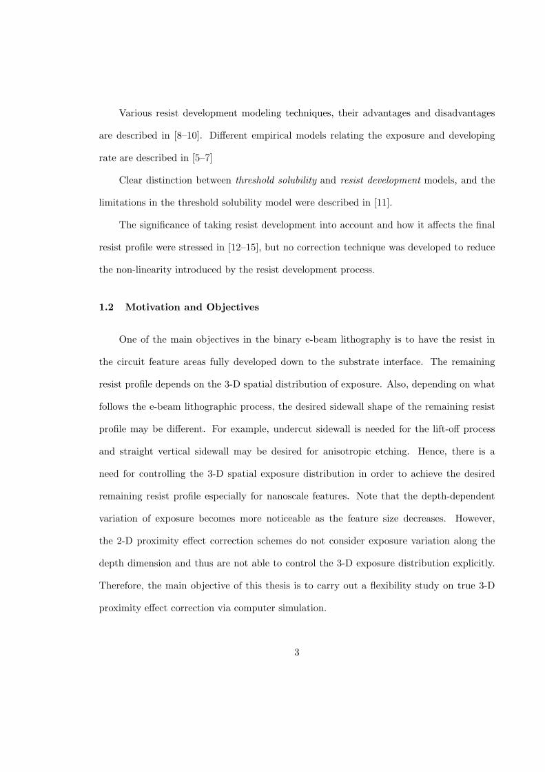
1.2 Motivation and Objectives
One of the main objectives in the binary e-beam lithography is to have the resist in
the circuit feature areas fully developed down to the substrate interface. The remaining
resist profile depends on the 3-D spatial distribution of exposure. Also, depending on what
follows the e-beam lithographic process, the desired sidewall shape of the remaining resist
profile may be different. For example, undercut sidewall is needed for the lift-off process
and straight vertical sidewall may be desired for anisotropic etching. Hence, there is a
need for controlling the 3-D spatial exposure distribution in order to achieve the desired
remaining resist profile especially for nanoscale features. Note that the depth-dependent
variation of exposure becomes more noticeable as the feature size decreases. However,
the 2-D proximity effect correction schemes do not consider exposure variation along the
depth dimension and thus are not able to control the 3-D exposure distribution explicitly.
Therefore, the main objective of this thesis is to carry out a flexibility study on true 3-D
proximity effect correction via computer simulation.
3

The main objectives of this thesis are:
• Analysis of the 3-D proximity effect in terms of the spatial distribution of exposure
in the resist through computer simulation.
• Development of the proof-of-concept 3-D proximity effect correction schemes using
iso-exposure contours and remaining resist profiles.
• Performance comparison of the 3-D proximity effect correction schemes over 2-D cor-
rection techniques through computer simulation.
1.3 Organization of the Thesis
This thesis is organized as follows:
• Chapter 2 introduces the 3-D exposure and resist development models.
• Chapter 3 analyzes the 3-D proximity effect (in terms of spatial exposure distribution
in the resist) considering the parameters such as beam energy, resist thickness, feature
size, developing threshold, etc.
• Chapter 4 describes the proof-of-concept implementation of 3-D proximity effect cor-
rection using the iso-exposure and resist profile models.
• Chapter 5 analyzes the performance of 3-D proximity effect correction schemes over
the 2-D correction scheme in terms of CD (Critical Dimension) or sidewall control.
• Chapter 6 presents conclusions and suggestions for future work.
• Appendix 1 includes some implementation issues, such as the unit of exposure and
value of constants used in the resist development simulation.
4

Chapter 2
Three-Dimensional Models
2.1 Electron Beam Lithography
Derived from early scanning electron microscopes, e-beam lithography uses a focused
electron beam to write circuit patterns in a resist sensitive to energy deposited by electrons.
As illustrated in Figure 2.1, the features in a pattern are exposed by e-beam and a
solvent developer is then used to selectively wash away the resist depending on the energy
deposited in it. For a positive resist, resist is washed away if the energy deposited is higher
than a certain threshold value (“developing threshold”). The exposure level is to be higher
than the threshold within each feature and lower than the threshold in the background (un-
exposed area) when a positive resist is used. After the development process, the developed
resist areas represent the copy of the written circuit pattern.
2.1.1 Proximity Effect Correction
Proximity effect in e-beam lithography is mainly due to the “non-ideal” distribution of
exposure (energy deposited in the resist). Therefore, it is necessary to control the distribu-
tion of exposure in the resist so as to obtain the desired pattern. One of the approaches in
proximity effect correction is dose modulation, wherein an optimal dose (energy incident in
the resist) is searched for each region to achieve the desired exposure distribution.
5

Resist
Substrate
1. Expose
2. Develop
Electron beam with different dose depending on the location
Figure 2.1: Illustration of a binary lithographic process.
2.1.2 Point Spread Function
Electron scattering can be modeled through an energy deposition profile or point spread
function (PSF), which shows how the energy is distributed in the resist when a single point
is exposed.
In general, the PSF is a function of the distance from the exposed point as well as
depth as shown in Figure 2.2-(a). Thus, the PSF is a radially symmetric three-dimensional
function. As illustrated in Figure 2.3-(a) and (b), the shape of a PSF depends on the
parameters resist thickness, substrate composition, beam energy, etc., but not on the dose
given to the point. For homogeneous substrates, the PSF shape does not vary with the
position of the point exposed. It can also be seen from Figures 2.2-(a), 2.3-(a) and (b),
that a PSF can be decomposed into two components, the local (or short ranged) component
6

and the global (or long ranged) component [45]. The local component, due to electron’s
forward scattering, has large magnitude and is very sharp while the global component, due
to electron’s backward scattering, has relatively low magnitude and is flat.
E-beam lithographic process can be assumed to be linear and space invariant for uni-
form substrates. Therefore, exposing a circuit pattern can be simulated by convolving
the circuit pattern with a PSF. The output of convolution represents the spatial exposure
distribution.
10−2
100
102
100
105
Radius (µm)
Exp
osu
re (
eV
/µm
3)
TopMiddleBottom
Radius (µm)
Re
sist
De
pth
(nm
)
−20 −10 0 10 20
100
200
300
400
500
(a) (b)
Figure 2.2: A PSF for the substrate system of 500 nm PMMA on Si with the beam energyof 50 keV: (a) the top, middle and bottom layers, and (b) all layers
2.2 2-D Exposure Model
In a 2-D exposure model, variation of the exposure distribution, e(x, y, z), along the
Z-axis is not considered (refer to Figure 2.4 for the axes convention). A 2-D point spread
function PSF (x, y) is used for the computation of exposure and is obtained by averaging
7

the 3-D point spread function PSF (x, y, z) over z i.e., PSF (x, y) = 1T
∫ T0 PSF (x, y, z)dz
where T is the thickness of resist. A 2-D PSF is as shown in Figure 2.3.
10−2
100
102
100
105
Radius (µm)
Exp
osu
re (
eV
/µm
3)
Figure 2.3: A 2-D PSF for the substrate system comprising 500 nm PMMA on Si with thebeam energy of 50 keV.
Thus, 2-D exposure distribution e(x, y) is given by
e(x, y) =∫x′
∫y′ PSF (x − x′, y − y′)f(x′, y′)dx′dy′, where f(x, y) represents the dose to
be given to each point (x, y) on the resist surface for writing a circuit pattern. But, the
actual profile of remaining resist can vary with z significantly due to the depth-dependent
exposure distribution. Therefore, proximity correction using a 2-D model would not lead
to an accurate result especially when a certain shape of sidewall of the remaining resist is
desired.
2.3 3-D Exposure Model
In 3-D exposure model, a 3-D point spread function PSF (x, y, z) is used as shown in
Figure 2.2-(a) and (b), and thus the depth-dependent proximity effect is considered.
8

width
X
Y
Z
Resist
Substrate
feature
T
Figure 2.4: A substrate system model consisting of a substrate and resist of thickness T .Substrate system is assumed to be spatially homogeneous, i.e., the substrate compositionand the resist thickness (T ) do not change with location. Z-axis represents the resist depth.
As illustrated in Figure 2.2-(a) and (b), a typical PSF shows a narrow high-amplitude
distribution of exposure in the top layer while a wide low-amplitude distribution in the
bottom layer. This depth-dependent energy spread in the resist leads to the 3-D proximity
effect which leads to variation of performance metrics with the resist depth. Since the PSF
is radially symmetric about Z-axis, PSF (x, y, z) may be expressed as PSF (√
x2 + y2, z) =
PSF (r, z) where r =√
x2 + y2.
Thus, the 3-D exposure e(x, y, z) is computed using the following convolution.
e(x, y, z) =∫
x′
∫
y′
∫
z′PSF (x− x′, y − y′, z − z′)f(x′, y′, 0)dx′dy′dz′
=∫
x′
∫
y′
∫
z′PSF (x− x′, y − y′, z − z′)f(x′, y′)δ(z′)dx′dy′dz′
=∫
x′
∫
y′PSF (x− x′, y − y′, z)f(x′, y′)dx′dy′ (2.1)
9

From Equation 2.1, it is seen that the exposure distribution at a certain depth (z0)
can be computed by the 2-D convolution between PSF (x, y, z0) and f(x, y, 0) in the corre-
sponding plane, z = z0. That is, e(x, y, z) may be estimated layer by layer.
Though the 3-D exposure model provides a complete information on how electron
energy is distributed in the resist, it does not directly depict the remaining resist profile
after development. In order to make correction results more realistic, one has to consider
the resist development process into account for correction.
2.4 Resist Development Model
0.4 0.6 0.8 1 1.2 1.40
0.02
0.04
0.06
0.08
0.1
0.12
Norm. Exposure (eV/µm3)
Rat
e (n
m/s
ec)
0 200 400 600 800 10000.4
0.6
0.8
1
1.2
1.4
Resist Depth(µm)
Nor
m. E
xpos
ure
(eV/
µm3 )
(a) (b)
Figure 2.5: Nonlinear relationship: (a) rate vs. 3-D exposure and (b) 3-D exposure vs.depth. Exposure is normalized by 1010. For a feature of width L: 50 nm, Dose: 200µC/cm2, 1000 nm PMMA on Si, 50 keV.
Most resists are nonlinear in nature when exposed by e-beam, i.e., the resist devel-
opment rate is not linearly proportional to exposure (see Figure 2.5-(a)). Exposure varies
with depth z (see Figure 2.5-(b)). Also, not all points in the resist are exposed to the
developer at the same time, i.e., the developing process is sequential from the top surface
of resist toward the bottom. Therefore, the remaining resist profile after development can
be significantly different from that estimated by the exposure models.
10

2.4.1 Model
To simulate the time evolution of the development profile of the resist, the exposure
matrix e(x, z) (eV/µm3) is transformed into a development rate matrix r(x, z) (nm/s). The
relationship between r and e is determined by experimental measurements of changes in
resist thickness as a function of development time for a particular resist-solvent combination.
After curve-fitting such data with an analytical expression, the relationship between r and
e is established.
The empirical model describing the relationship between r and e for the polymethyl
methacrylate (PMMA) resist is given by Equation 2.2 [5].
ri,j = r0 + B(1
Mn+
g · ei,j · 1012
ρ ·NA)A (2.2)
where (i, j) is the index of cell, Mn is the original number average molecular weight, g is the
chain scission per electron volt absorbed (/eV), e is the exposure (eV/µm3), ρ is the resist
polymer mass density (g/cm3), NA is the Avogadro’s number (= 6.023×10²³molecules/g−
mol).
The constants r0, A, and B are empirically determined for PMMA with different sol-
vents (see Section A.2). Typical values for PMMA are g = 1.9 × 10⁻²/eV (proposed by
Greeneich), Mn=50000, and ρ = 1.19g/cm3.
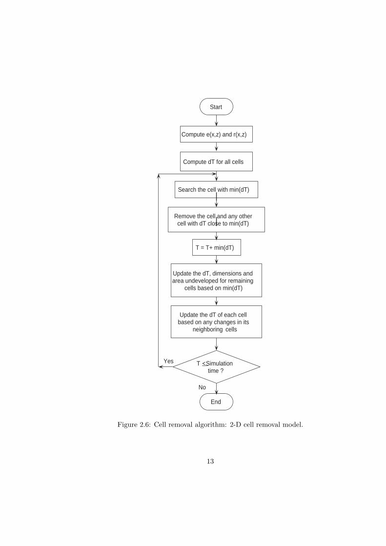
2.4.2 Simulation (Cell Removal Model)
In this thesis, a simplified version of the “cell removal algorithm” [8,9] is implemented
because it is the most robust and numerically stable of all resist development algorithms.
11

In the simplified cell removal algorithm, only a line feature is considered, which is long
enough in the Y -dimension that any variation along Y -axis is ignored. Thus, the solubility
rate and exposure matrices are functions of x and z only. The resist is divided into m× n
cells in the X-Z dimension.
The reaction of developer is assumed to take place only along the normals of the cell
sides. Cells are removed by the developer, one after another, according to their dissolution
time dT and the number of sides in contact with the developer. When a cell is removed, the
new cells exposed start developing. Any cells having an additional side exposed have their
projected time of removal updated based on Equations 2.3, 2.4, and 2.5. Thus, by keeping
track of the cells in contact with developer and their associated sides, the cell removal
algorithm is able to simulate the development process. The result of the simulation is the
development matrix, which contains the percentage development of each cell.
Thus, 2-D development algorithm as shown in Figure 2.6 involves three main steps:
• Finding the minimum dT cell and dissolving it;
• Updating the dT of other cells for the elapsed time;
• Based on the status of its neighbors, compute/recompute the time of dissolution (dT )
for all undeveloped cells using Equations 2.3, 2.4, and 2.5.
Thus, the cells are removed in the order that the development proceeds.
The dissolution or development time dT of a cell is derived as follows for each condition
of the cell based on its neighbors [9].
Case 1: Single side development: When a single side of a cell is exposed to a developer
as shown in Figure 2.7-(a), (b), and (c), then the dissolution time dT of cell (i, j) is
12
Search the cell with min(dT)
Remove the cell and any other cell with dT close to min(dT)
T = T+ min(dT)
Update the dT, dimensions and area undeveloped for remaining
cells based on min(dT)
Update the dT of each cell based on any changes in its
neighboring cells
Start
Compute e(x,z) and r(x,z)
T < Simulation time ?
End
No
Yes
Compute dT for all cells
Figure 2.6: Cell removal algorithm: 2-D cell removal model.
13

(i, j ) (i, j ) (i, j )
(i, j )
(i, j ) (i, j ) (i, j )
Case 1
Case 2
Case 3
(a) (b) ( c )
(d) ( e ) ( f )
( g )
Figure 2.7: Status of cell (i, j) where Case 1: (a),(b) and (c) single side development; Case2: (d),(e), and (f) double side development; Case 3: (g) triple side development. Unshadedare the developed cells and shaded are the undeveloped cells. Arrow heads point in thedirection of developer flow.
14

dTi,j =dxi,j · dzi,j
dsi,j · ri,j(2.3)
where dx is the width, dz is the height and r is the rate of cell (i, j) and ds is the dimension
dx or dz of the exposed side.
Case 2: Double side development: When two neighboring sides (for example, the dx and
dz side) of a cell are exposed to the developer as shown in Figure 2.7-(d), (e), and (f), then
the development time dT is accelerated for cell (i, j) as follows,
dTi,j =dxi,j · dzi,j√
dx2i,j + dz2
i,j · ri,j
(2.4)
where√
dx2i,j + dz2
i,j is the modulation factor representing the acceleration introduced by
two sides exposed.
Case 3: Triple side development: When three neighboring sides (for example, the two
dz and dx) of a cell (i, j) are exposed as shown in Figure 2.7-(g), then the development time
dT is accelerated for cell (i, j) as follows,
dTi,j =dxi,j · dzi,j√
dx2i,j + dz2
i,j + dz2i,j · ri,j
(2.5)
where√
dx2i,j + dz2
i,j + dz2i,j is the modulation factor representing the acceleration intro-
duced by three sides exposed.
In the implemented cell removal model, cells are assumed to be rectangular with default
cell dimensions dx = 5 nm and dz = 10 nm where dx depends on the pixel size and dz is
the distance by which the 3-D PSF is sampled along the Z-axis.
15

Chapter 3
Analysis of Three-Dimensional Proximity Effect in E-Beam Lithography
In this chapter, the three-dimensional (3-D) proximity effect is studied through sim-
ulation using the 3-D exposure model described in Chapter 2, when the desired sidewall
is vertically straight. The effects of the parameters such as beam energy, resist thickness,
feature size, developing threshold, etc. on the 3-D spatial distribution of exposure in the
resist, in particular, depth-dependent proximity effect, are considered in the analysis. The
remaining resist profile after development is mainly determined by the spatial distribution
of exposure though the development process can also affect the profile which is studied in
detail in Chapters 4 and 5.
3.1 Intra-Proximity Effect
The intra-proximity effect refers to the proximity effect within a feature. In order
to quantify the 3-D intra-proximity effect, the two metrics, width variation and exposure
contrast, are introduced.
Width Variation
The width of a line feature may vary with the resist depth after development as illus-
trated in Figure 3.1. The line feature is long enough in the Y direction that its width can
be assumed not to vary with y. Let W (z) denote the width of the line feature where z is
the depth in the resist. In this simulation study, it is assumed that W (z) can be approxi-
mated by the iso-exposure contour determined by e(x, z) = Thr where Thr is the developing
16

threshold (refer to Figure 3.4-(b)). Note that e(x, y, z) does not vary with y in the middle
of the line. Let Wt and Wb represent the widths of the line at the top and bottom layers
of resist, respectively, i.e., Wt = W (0) and Wb = W (T ) where T is the thickness of resist.
Also, the average width, w, of the line is defined to be 1T
∫ T0 W (z)dz. Width variation, δw,
quantifies deviation from the straight vertical sidewall, and is defined to be Wt−WbW . Note
that δw > 0 and δw < 0 indicate overcut and undercut, respectively. When the sidewalls
are vertically straight, δw = 0. That is, the measure of δw can not only quantify the width
variation, but also indicate the type of sidewall.
Wb
Wt
Resist
Substrate
Z
X
W(z)
Wb
Resist
Substrate
W(z)
Wt
T
(a) (b)
Figure 3.1: Cross-section of the remaining resist for a line feature: (a) overcut (δw > 0) and(b) undercut (δw < 0).
Exposure Contrast
For a long line feature along the Y axis, exposure contrast (or gradient), C(z), is
defined as |∂e(x,y,z)∂x |e=Thr|. Given a developing threshold Thr, the iso-exposure contour
of e(x, z) = Thr is determined on the X-Z plane. Then, C(z) is computed across the
iso-exposure contour, i.e., it quantifies how fast the exposure changes spatially around the
developing threshold. The exposure contrast needs to be higher for a smaller variation of
17

the feature dimension due to the varying development process. The exposure contrast varies
with the resist depth.
3.2 Inter-Proximity Effect
Wt1 Wt2 Wt3
Wb1 Wb2 Wb3
Wm1 Wm2 Wm3
Figure 3.2: Variation of line width due to inter-proximity effect among multiple lines whenδwi > 0 for all i.
r (x)a
r (x)d
Figure 3.3: Comparison of the remaining resist profile (ra(x)) with the desired one (rd(x)of “straight vertical sidewalls”) where the difference between the two profiles is shown asthe shaded areas. The ratio of line to space (L:S) is 1:1.
When multiple features are close to each other, the interaction among them leads to
the inter-proximity effect [25]. The level of inter-proximity effect varies with depth in the
resist since the exposure distribution, e(x, y, z), is a function of the resist depth, z. This
3-D inter-proximity effect makes the line width vary spatially and the amount of variation
depends on the resist depth. As one way to quantify the 3-D inter-proximity effect, the
18

spatial variation of line width among lines is considered for a uniform typical line-space
pattern. Let Wti, Wmi and Wbi denote the widths of the ith line at the top, middle,
and bottom layers, respectively, as illustrated in Figure 3.2. Then, for the top layer, the
normalized standard deviation of Wti is computed as σwt = 1W t
√1N
∑Ni=1(Wti −W t)2 where
W t is the mean of Wti among the lines, i.e., W t = 1N
∑Ni=1 Wti and N is the number of lines.
Similarly, for the middle and bottom layers, σwm and σwbmay be computed from {Wmi}
and {Wbi}, respectively. For a non-uniform pattern, e.g., the line width varies with line, Wti
(Wmi, Wbi) may be normalized by the average width of the ith line, wi = 1T
∫ T0 Wi(z)dz,
before σw is computed. Note that this measure (σw) of inter-proximity effect only quantifies
how uniform the remaining resist profile is among multiple features. It does not directly
indicate the deviation from a desired profile.
When a desired profile is known, a quantitative measure of difference between the
desired and actual profiles can be defined to supplement the measure of σw. Let rd(x)
and ra(x) depict the desired and actual profiles, respectively, as illustrated in Figure 3.3.
Note that ra(x) is the iso-exposure contour of e(x, z) = Thr. Then, the difference (or error)
measure may be computed as ε = 1XT
∫ X0 |ra(x)−rd(x)|dx where X is the width of a pattern
(e.g., for 3 lines of width L, and 3 spaces of width S, X = 3(L + S)).
3.3 Simulation Results and Discussion
The simulation model employed in this study takes only exposure into account. 3-D
exposure distribution in the resist is computed by the layer-by-layer 2-D convolution which
is accelerated by the CDF (Cumulative Distribution Function) table method [45]. Changing
the base dose (“dose” hereafter), i.e., changing the dose distribution uniformly, simply scales
19

the exposure distribution. Hence, analyzing effects of different doses may be carried out
by considering different developing thresholds for the same exposure distribution. This
eliminates the need to repeat the same convolution with different scaling factors in the
simulation. In all cases, exposure was computed at 10 layers of resist, which are equally
spaced.
3.3.1 Iso-Exposure Contours
X (µm)
Res
ist D
epth
(nm
)
0.14 0.16 0.18 0.2
100
200
300
400
500
X (µm)
Res
ist D
epth
(nm
)
18
16
14
12
10
2
24
6
884
0.14 0.16 0.18 0.2
100
200
300
400
500
(a) (b)
Figure 3.4: Cross-sections (X-Z plane) of exposure distribution in the resist when a rect-angular feature with the width (L) of 50 nm is exposed with the dose of 200 µC/cm2: (a)grayscale image and (b) iso-exposure contours. The substrate system consists of 500 nmPMMA on Si and the electron beam energy is 50 keV. The unit of exposure is µC/cm2.
In Figure 3.4, the cross-section e(x, z) of spatial exposure distribution is shown for a
rectangular circuit feature when the dose is 200 µC/cm2 (refer to Figure 2.4). It can be seen
that the exposure distribution varies with the resist depth. The iso-exposure contour plot in
Figure 3.4-(b) indicates that the remaining resist profile can be quite different depending on
the dose or developing threshold. Suppose that the developing threshold is 8 µC/cm2. Then,
in order to achieve the vertical sidewalls, the dose needs to be doubled (to 400 µC/cm2).
Note that the contour of 4 µC/cm2 is almost vertical in Figure 3.4-(b). In addition to the
20

line width variation, one can also see the dependency of exposure contrast on the resist
depth, i.e., higher at the top layer than at the bottom layer. In Figure 3.5, dependency
of the line width on the resist depth is shown for two different thicknesses of resist. The
line width varies significantly with the resist depth and the variation is larger for a thicker
resist.
0.05 0.1 0.15 0.2 0.25 0.30
10
20
X (µm)
Exp
.(µ
C/c
m3)
0.05 0.1 0.15 0.2 0.25 0.30
10
20
X (µm)
Exp
.(µ
C/c
m3)
0.05 0.1 0.15 0.2 0.25 0.30
10
20
X (µm)
Exp
.(µ
C/c
m3)
0.05 0.1 0.15 0.2 0.25 0.30
10
20
X (µm)
Exp
.(µ
C/c
m3)
0.05 0.1 0.15 0.2 0.25 0.30
10
20
X (µm)E
xp
.(µ
C/c
m3)
0.05 0.1 0.15 0.2 0.25 0.30
10
20
X (µm)
Exp
.(µ
C/c
m3)
(a) (b)
Figure 3.5: Dependency of line width (after development) on resist depth (top, middleand bottom layers) for the substrate system of PMMA on Si and 50 keV with the dose of200 µC/cm2: (a) 500 nm PMMA and (b) 1000 nm PMMA. The developing threshold is 8µC/cm2.
3.3.2 Intra-Proximity Effect
Resist Thickness
In Figure 3.6, iso-exposure contours are plotted for two different thicknesses of resist.
When the resist is 100 nm thick, the contours show little variation along the depth dimension
(refer to Figure 3.6-(a)), i.e., not much 3-D proximity effect. However, as the resist thickness
21

2 2
4 4
6 6
10
10
12
12
16
1617
X (µm)
Res
ist D
epth
(nm
)
0.14 0.16 0.18 0.2
20
40
60
80
100
24
4
6
6
8
101416
X (µm)
Res
ist D
epth
(nm
)
0.14 0.16 0.18 0.2
200
400
600
800
1000
(a) (b)
Figure 3.6: Dependency of iso-exposure contours on the resist thickness: (a) 100 nm PMMAon Si and (b) 1000 nm PMMA on Si. The unit of exposure is µC/cm2. L: 50 nm, dose:200 µC/cm2, 50 keV.
0 200 400 600 800 1000−0.5
0
0.5
1
1.5
Resist Thickness (nm)
δ w
Thr=4 µC/cm2
Thr=6 µC/cm2
Thr=8 µC/cm2
0 200 400 600 800 10000
0.5
1
1.5
2
x 107
Resist Thickness(nm)
C(z
) (µC
/cm
3 )
TopMiddleBottom
(a) (b)
Figure 3.7: Dependency of δw and C on the resist (PMMA) thickness: (a) δw and (b) C(Thr = 2µC/cm2). L: 50 nm, dose: 200 µC/cm2, 50 keV.
22

increases, the 3-D proximity effect becomes larger, leading to a significant depth-dependent
variation in exposure distribution as shown in Figure 3.6-(b) where the resist thickness
is 1000 nm. In Figure 3.7, the line width variation (δw) and exposure contrast (C) are
analyzed by varying the resist thickness. As the resist thickness increases, δw becomes
larger as expected (Figure 3.7-(a)). It is also seen that δw is larger for a higher (developing)
threshold (equivalently a lower dose for a fixed threshold). In Figure 3.7-(b), it is observed
that C decreases as the resist thickness increases since the electron energy spreads more for
a thicker resist. The decrease in the exposure contrast is more evident in the lower layers.
Beam Energy
X (µm)
Res
ist D
epth
(nm
)
2
4
6
8
1012
0.14 0.16 0.18 0.2
100
200
300
400
500
X (µm)
Res
ist D
epth
(nm
)
2 2
4 4
6
8
10
12
0.14 0.16 0.18 0.2
100
200
300
400
500
(a) (b)
Figure 3.8: Dependency of iso-exposure contours on the beam energy: (a) 5 keV and (b)20 keV. The unit of exposure is µC/cm2. Dose: 200 µC/cm2, L: 50 nm, 500 nm PMMAon Si.
Dependency of the iso-exposure contours on the beam energy is shown in Figure 3.8
(also refer to Figure 3.4-(b)). As the beam energy increases, electrons can penetrate deeper
into the resist leading to a more vertical orientation of the contours, which makes δw smaller.
23

However, the beam energy higher than a certain value may be lead to an undercut due to
excessive backscattering from the substrate depending on the resist thickness.
Feature Size
X (µm)
Res
ist D
epth
(nm
)
18
16
14
12
10
2
24
6
884
0.14 0.16 0.18 0.2
100
200
300
400
500
X (µm)
Res
ist D
epth
(nm
)
18
16
14
12
2
2
12104 6
6
0.1 0.2 0.3 0.4 0.5 0.6
100
200
300
400
500
(a) (b)
Figure 3.9: Dependency of iso-exposure contours on feature size (L: line width): (a) L =50 nm and (b) L = 400 nm. The unit of exposure is µC/cm2. Dose: 200 µC/cm2, 500 nmPMMA on Si, 50 keV.
In Figure 3.9, iso-exposure contours are compared for two different feature sizes (line
widths). When the feature size is small as in Figures 3.9-(a), the exposure variation along
the depth dimension is significant. However, for large features, the variation is relatively
small as can be seen in Figure 3.9-(b). Note that the exposure difference between the top
and bottom layers is about 10 and 6 µC/cm2 for the small and large features, respectively.
Threshold
As mentioned earlier, increasing (or decreasing) the dose with a fixed developing thresh-
old is equivalent to decreasing (or increasing) the threshold with a fixed dose. In Figure
3.10, effects of the threshold (dose) on δw and C are analyzed. For a higher threshold (a
lower dose), δw is larger, i.e., the line width varies more with the resist depth as shown
24

in Figure 3.10-(a). Also, the remaining resist profile tends to be overcut (δw > 0). As
the threshold decreases (the dose increases), δw decreases. Particularly for a high beam
energy, δw can become negative, i.e., the remaining resist profile of undercut. The exposure
contrast, C, is shown in Figure 3.10-(b). It is seen that the exposure contrast is highest
at the top layer, and decreases as the resist depth increases. In a layer, as the threshold
increases, C shows a bitonic behavior, i.e., an increasing interval followed by a decreasing
interval. This is due to the typical characteristics of spatial exposure distribution over the
feature edges (refer to Figure 3.5 noting that C is an exposure gradient).
5 10 15−1
−0.5
0
0.5
1
1.5
Thr (µC/cm2)
δ w
5keV20keV50keV
0 5 10 150
0.5
1
1.5
2
2.5
3
3.5x 10⁷
Thr (µC/cm2)
C(z
) (µC
/cm
3 )
TopMiddleBottom
(a) (b)
Figure 3.10: Dependency of δw and C on threshold or equivalently dose: (a) δw and (b) C(exposure contrast). Dose: 200 µC/cm2, L: 50 nm, 500 nm PMMA on Si, 50 keV.
3.3.3 Inter-Proximity Effect
Variation of Line Width and Exposure Contrast
As shown in Figure 3.11, the width variation (σw) among the (three) lines due to inter-
proximity effect is largest at the bottom layer and least at the top layer. This is due to the
fact that energy spread due to electron scattering is greater at a lower layer of resist. Also,
as the resist thickness increases or the beam energy decreases, σw increases significantly
25

0 200 400 600 800 10000
0.01
0.02
0.03
0.04
0.05
0.06
Resist Thickness(nm)
σ w
TopMiddleBottom
0 20 40 600
0.01
0.02
0.03
0.04
0.05
0.06
Beam Energy(keV)σ w
TopMiddleBottom
(a) (b)
0 50 100 1500
0.02
0.04
0.06
0.08
0.1
Space (nm)
σ w
TopMiddleBottom
(c)
Figure 3.11: Dependency of σw on (a) resist thickness, (b) beam energy (S=100nm, Thr =4µC/cm2, T = 500 nm), and (c) S (Thr = 9µC/cm2, T = 500 nm). Dose: 200 µC/cm2,L: 50 nm, 50 keV, PMMA on Si.
26

except for the top layer where the exposure contrast is highest. In particular, as the space
(S) between lines decreases, the inter-proximity effect increases, which makes σw larger.
The increase is greater at the bottom layer (than at the top layer). Also, it is observed that
the exposure contrast (C) has a larger deviation among the lines for a lower layer, a thicker
resist, and a smaller line spacing.
Error in Resist Profile
0 5 10 150
0.1
0.2
0.3
0.4
0.5
Thr (µC/cm2)
ε
T=100 nmT=500 nmT=1000 nm
0 5 10 150
0.1
0.2
0.3
0.4
0.5
Thr (µC/cm2)
ε
S=25 nmS=50 nmS=100 nm
0 5 10 150
0.1
0.2
0.3
0.4
0.5
Thr (µC/cm2) ε
5keV20keV50keV
(a) (b) (c)
Figure 3.12: Dependency of ε on (a) resist thickness (50 keV ), (b) S (50 keV ), and (c)beam energy. Dose: 200 µC/cm2, L: 50 nm, 500 nm PMMA on Si, Thr : 4µC/cm2.
In Figure 3.12, the error, ε, between the desired and actual remaining resist profiles is
analyzed when the desired profile has straight vertical walls. It is observed that there exists
a threshold (equivalently a dose) which minimizes the error. As expected, the error is larger
for a thicker resist as shown in Figure 3.12-(a). As the (three) lines get closer, i.e., the
space, S, between lines decreases, a higher level of inter-proximity effect is incurred leading
to a larger error. Low-energy electrons cannot penetrate deep into the resist. Hence, the
minimum ε one can achieve by controlling the dose is significantly larger for a lower beam
energy than a higher beam energy as seen in Figure 3.12-(c).
27

Undercut/Overcut
X (µm)Re
sist D
epth
(nm
)
24
810
12
141618
8
64
26
8 10
12
16
2
46
6
10
24
8
14
18
0.1 0.15 0.2 0.25 0.3 0.35 0.4
100
200
300
400
500
(a)
X (µm)
Res
ist D
epth
(nm
)
0.1 0.2 0.3 0.4
100
200
300
400
500
X (µm)
Res
ist D
epth
(nm
)
0.1 0.15 0.2 0.25 0.3 0.35 0.4
100
200
300
400
500
(b) (d)
X (µm)
Res
ist D
epth
(nm
)
0.1 0.15 0.2 0.25 0.3 0.35 0.4
100
200
300
400
500
X (µm)
Res
ist D
epth
(nm
)
0.1 0.15 0.2 0.25 0.3 0.35 0.4
100
200
300
400
500
(c) (e)
Figure 3.13: Dependency of the remaining resist profile on developing threshold: (a) expo-sure contours, (b) Thr = 18 µC/cm2, (c) Thr = 12 µC/cm2, (d) Thr = 9 µC/cm2, and(e) Thr = 2 µC/cm2. Dose: 200 µC/cm2, L: 50 nm, S: 25 nm, 500 nm PMMA on Si, 50keV. The dashed lines show the ideal line widths.
In Figures 3.13 and 3.14, the profile of remaining resist is examined by changing the
threshold (dose) or line spacing. It is illustrated that the inter-proximity effect becomes
visible when the dose is increased or the space between lines is decreased. Also, it is to be
noted that the inter-proximity effect is layer-dependent and is most severe at the bottom
layer. As the dose is increased (i.e., the threshold is decreased), the level of inter-proximity
effect increases especially at the lower layers and eventually the three lines are merged due
to the undercut at the lower layers while still separated at the upper layers as shown in
28

X (µm)
Res
ist D
epth
(nm
)
0 0.1 0.2 0.3 0.4 0.5 0.6
20406080
100
X (µm)
Res
ist D
epth
(nm
)
0.1 0.2 0.3 0.4 0.5
20406080
100
(a) (b)
X (µm)
Res
ist D
epth
(nm
)
0 0.1 0.2 0.3 0.4 0.5
20406080
100
X (µm)
Res
ist D
epth
(nm
)
0.1 0.2 0.3 0.4
20
40
60
80
100
(c) (d)
Figure 3.14: Dependency of the remaining resist profile on line spacing (S): (a) & (b)S = 100 nm and (c) & (d) S = 25 nm. Dose: 200 µC/cm2, Thr = 10 µC/cm2, L: 50 nm,100 nm PMMA on Si, 5 keV .
Figure 3.13. Similar observations can be made when the lines get closer to each other as
shown in Figure 3.14.
2-D vs. 3-D
In the simulation where a 2-D model is employed, any variation (of exposure) along
the depth dimension (Z) is not taken into consideration or assumed to be zero. Therefore,
equivalently, the remaining resist profile is completely vertical i.e. the equivalent 3-D expo-
sure e(x, z) is obtained from 2-D exposure e(x) by replicating the 2-D exposure values e(x)
along the depth of the resist.
3.3.4 Exposure
In Figure 3.15, the 2-D (dashed lines) and 3-D (solid lines) models are compared in
terms of the remaining resist profile. In Figure 3.15-(a) where S = 100 nm and the threshold
29

is 7 µC/cm2, the 2-D model estimates the line width to be about 35 nm. However, the
profile estimated by the 3-D model shows that the line width is wider (than that estimated
by the 2-D model) in the top half of the resist layers and then becomes narrower, i.e.,
an overcut. Also, the bottom one third of resist layers is not even developed. When the
threshold is lowered (or the dose is increased), overcuts may become undercuts and wider
line widths may result at lower layers in the 3-D model as shown in Figure 3.15-(b). Also,
it should be noticed that the center line is wider than the other two “end lines” at the
bottom of resist. In addition, the centers of the end lines are shifted toward the center line
more at the bottom of resist than at the top. For an even lower threshold as in Figure
3.15-(c), the lines are merged at the lower layers according to the 3-D model while they are
well separated in the 2-D profile. When S = 25 nm, the inter-proximity effect is greater,
however, similar observations can be made as shown in Figures 3.15-(d), (e) and (f). In
Figure 3.15-(f), the 2-D model indicates that all three lines are completely merged while
the 3-D model shows some undeveloped resist between the lines except at few lower layers.
It is clear that the 2-D and 3-D models lead to significantly different estimation results.
In particular, the 2-D model is not able to distinguish the overcut and undercut from the
vertical straight wall.
3.3.5 Resist Development Profile
Shown in Figure 3.16-(a) and (b) are the 2-D exposure distribution and its correspond-
ing development contours. It is seen that 2-D model fails to depict the intra-proximity effect
in the feature and thus inaccurately predicts the remaining resist profiles. Also, shown in
Figure 3.16-(c) and (d) are the 3-D exposure distribution and its development contours.
30

X (µm)
Res
ist D
epth
(nm
)
0.1 0.2 0.3 0.4 0.5 0.6
200
400
600
800
1000
X (µm)
Res
ist D
epth
(nm
)
0.1 0.2 0.3 0.4
100
200
300
400
500
(a) (d)
X (µm)
Res
ist D
epth
(nm
)
0.1 0.2 0.3 0.4 0.5 0.6
200
400
600
800
1000
X (µm)
Res
ist D
epth
(nm
)
0.1 0.2 0.3 0.4
100
200
300
400
500
(b) (e)
X (µm)
Res
ist D
epth
(nm
)
0.1 0.2 0.3 0.4 0.5 0.6
200
400
600
800
1000
X (µm)
Res
ist D
epth
(nm
)
0.1 0.2 0.3 0.4
100
200
300
400
500
(c) (f)
Figure 3.15: Comparison of remaining resist profiles between 2-D (dashed) and 3-D (solid)models using iso-exposure contours. For S: 100 nm (1000 nm PMMA on Si), (a) Thr =7µC/cm2, (b) Thr = 3µC/cm2 and (c) Thr = 1.5µC/cm2. For S: 25 nm (500 nm PMMAon Si), (d) Thr = 10µC/cm2, (e) Thr = 5µC/cm2 and (f) Thr = 4µC/cm2. Dose: 200µC/cm2, L: 50 nm, 50 keV .
31

X (µm)
Res
ist D
epth
(nm
)
0.2
0.6 1
0.05 0.1 0.15
200
400
600
800
1000
X (µm)
Res
ist D
epth
(nm
)
0.05 0.1 0.15
200
400
600
800
1000
5
65
86.6
50
25
(a) (b)
X (µm)
Res
ist D
epth
(nm
)
0.2
0.6
1
1.4
1.8
0.05 0.1 0.15
200
400
600
800
1000
X (µm)
Res
ist D
epth
(nm
)
0.02 0.04 0.06 0.08 0.1 0.12 0.14 0.16 0.18
200
400
600
800
1000
5
25
146.3
45
100
76
(c) (d)
Figure 3.16: Comparison of remaining resist profiles between 2-D ((a) and (b)) and 3-Dmodels ((c) and (d)) using resist development contours for different development times(min). (a) 2-D iso-exposure and (b) development contours using 2-D PSF, (c) 3-D iso-exposure and (d) development contours using 3-D PSF for a rectangular feature of width(L):100 nm, Dose: 300 µC/cm2, 1000 nm PMMA on Si, 50 keV. The unit of exposure iseV/µm3 normalized by 1010.
32

It is seen that no remaining resist profile (development contour) matches any iso-exposure
contour. Also, it is observed that the shape of remaining resist profile depends on the
development time. Therefore, in order to develop an accurate 3-D correction scheme, one
needs to consider the remaining resist profile instead of exposure contours.
33

Chapter 4
Three-Dimensional Correction Approaches
In this chapter, 3-D correction methods which use a 3-D exposure model in controlling
the e-beam dose distribution within each circuit feature to achieve the desired sidewall
profile are described.
The following two proof-of-concept implementations of 3-D proximity effect correction
for binary circuits, developed based on PYRAMID [45,52–55,57], are presented:
• 3-D iso-exposure contour correction (pre-development exposure contour)
• 3-D resist profile correction (post-development resist contour)
The prototype versions consider the exposure only along the cross-section of line pat-
terns for correction, under the assumption that the feature is sufficiently long along the
Y -dimension.
4.1 PYRAMID Correction Procedure
Figure 4.1 shows the basic correction procedure of the binary PYRAMID. First, a
circuit pattern is loaded from an input file. The input file includes a set of rectangles that
represent the boundaries of features. In the rectangle partitioning step, an input rectangle
may be partitioned into smaller rectangles if necessary. A rectangle is further partitioned
into multiple regions in the region partitioning step. A region is the smallest spatial unit
in controlling dose. Within each region, dose is constant and equal to the product of dose
factor and the base dose. In binary circuits, a rectangle is partitioned into center and
34

Set initial dose factor
Calculate global exposure
Calculate total exposure from local exposure and global exposure at the critical
point of a region
Determine the dose factor from the exposure and the required exposure of the region
Start
Region Partitioning
All regions are corrected?
End
No
Yes
Rectangle Partitioning
Take input parameters Load input circuit and PSF
All rectangles are corrected?
Meet termination condition?
Output correct circuit and other files for analysis
Basic iterative correction
Yes
Yes
No
No
Figure 4.1: The basic correction procedure of dose modification PYRAMID for binarycircuit patterns.
35

boundary regions. The center region’s exposure is targeted for a minimum exposure of
ThrC, while for boundary regions, it is targeted for ThrB, where ThrB < ThrC. Each
region contains a critical point. Critical points serve as the control points in the PYRAMID
approach, where accuracy of the correction result is evaluated.
After setting the initial dose factor for every region, an iterative nonrecursive correction
is performed for the entire circuit as shown in Equation 4.1.
Dadj =
Fadj · (Dtmp −Dold) + Dold if Dadj ≥ 0
0 if Dadj < 0(4.1)
where Dold is the dose factor in the previous iteration, Dtmp is the dose factor computed
in the current iteration, Fadj is the adjustment factor, and Dadj is the new adjusted dose
factor for the region.
In each iteration, all regions are corrected by the dose modification algorithm shown
in Figure 4.2. The adjusted dose factor for each region is computed such that the CD error
at the critical point(s) is minimized. The iteration continues until a certain termination
condition is met. The termination condition could be a certain number of iterations com-
pleted, having found an acceptable solution or that the correction procedure cannot further
improve the solution.
4.2 3-D Iso-Exposure Contour Correction
Developed from the previous dose modification PYRAMID for binary correction, the
3-D iso-exposure contour correction adopts an iso-exposure contour to fit to the desired
remaining resist profile. The exposure estimation is modified along with the location of
36

For each iteration: For each rectangle: Find the Exposure E c at the center region R c ;
Set dose D c of R c such that E c is at least ThrC
where ThrC is the desired exposure for the center region; For each other region R i where i =1 to n:
Find exposure E i at the boundary location ;
Set dose D i of R i such that E i = ThrB
where ThrB (< ThrC) is the development threshold ;
Figure 4.2: Dose modification algorithm for binary lithography. All the resist above thedeveloping threshold ThrB gets dissolved off by proper selection of solvent.
critical points and dose calculation. Each region is corrected using the 3-D exposure model
described in Section 2.3. The goal of the 3-D correction scheme is to match an iso-exposure
contour to the shape of the sidewall that needs to be achieved.
In binary circuits, three kinds of sidewalls are possible, namely, undercut, vertical,
and overcut. Critical points are located in the 3-D space and their locations depend on
the shape of the sidewall as shown in Figure 4.3. Two critical points are chosen, as in
the earlier version of PYRAMID, one inside (InLcn) and the other outside (OutLcn) the
desired sidewall of the feature. For vertical sidewall, the horizontal location of critical point
in a resist layer does not change with layer as shown in Figure 4.3-(b). For undercut, the
critical points are shifted out with reference to the feature boundary by a larger amount for
a lower layer as shown in Figure 4.3-(a) while for overcut, the critical points are shifted in
with reference to the feature boundary by a smaller amount for a lower layer as shown in
Figure 4.3-(c).
37

(a) (b)
Critical Point (InLcn)
Critical Point (OutLcn)
(c)
Figure 4.3: Cut-view (X − Z) of a feature to show sidewall shape and its correspondingcritical points setup: (a) Undercut, (b) Vertical, and (c) Overcut. Two critical points areused, one inside (InLcn) and the other outside (OutLcn) the desired sidewall. Dotted linesare the PSF layers, dashed lines are the feature boundaries, and bold continuous lines arethe desired sidewall boundaries.
38

In the current implementation, an iterative optimization approach is adopted where
the cost function to be minimized is given by Equation 4.2,
Costfunction(df) =9∑
i=0
(ER(zi)−Eiso(z)) (4.2)
where depth index i varying from 0 to 9, ER(zi) is the exposure computed at the critical
point for a region at depth zi, and Eiso(z) is the iso-exposure.
Figure 4.4 shows the optimization approach to determine the optimal dose factor that
minimizes the exposure error. Only the top, middle and bottom PSF layers are used in
order to save computation time and memory. Accuracy will improve if all the PSF layers
are used for correction.
After setting the initial dose factor for each region, the iterative correction is performed
until any increase in average (or maximum) exposure error between iterations or the maxi-
mum number of iterations is reached. In each iteration, all regions are corrected. Exposure
(local and global) is computed using the PSF layer corresponding to the location of critical
point in the 3-D sidewall. Then optimal dose factor for each region is then searched for,
which minimizes the cost function given in Equation 4.2.
Thus, the problem of finding a dose distribution to reduce the exposure error belongs
to the class of NP hard problems (in fact all 3-D correction schemes) and hence a solution is
searched by heuristics. The iso-exposure correction problem is approached as a constrained
optimization problem wherein an optimal dose factor for each region is searched for, which
minimizes the cost function (see Equation 4.2).
The fundamental problem with the 3-D iso-exposure correction (in fact all 3-D cor-
rection schemes) is when the thickness of the resist increases, the critical points located at
39
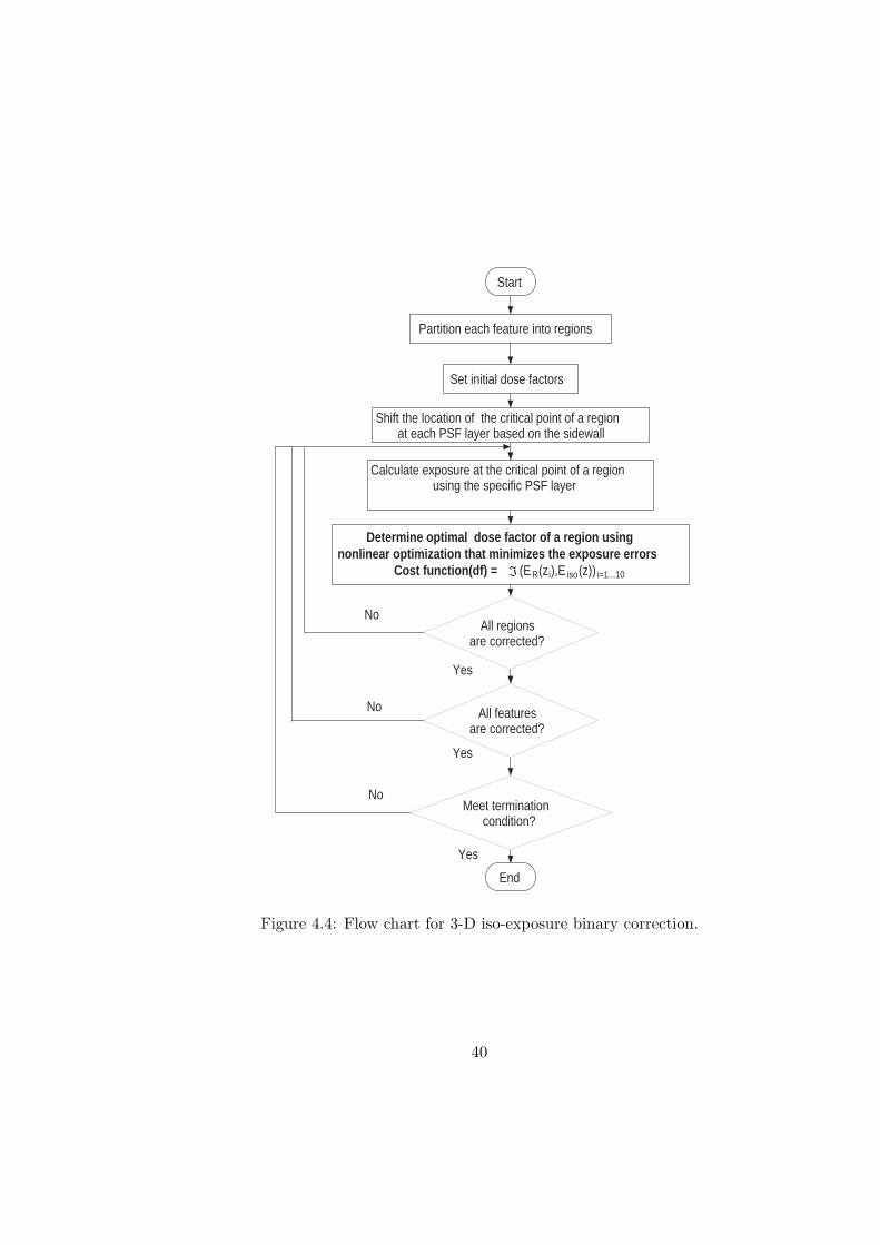
Start
Partition each feature into regions
All regions are corrected?
End
Set initial dose factors
Calculate exposure at the critical point of a region using the specific PSF layer
Meet termination condition?
Yes
All features are corrected?
Shift the location of the critical point of a region at each PSF layer based on the sidewall
Determine optimal dose factor of a region using nonlinear optimization that minimizes the exposure errors
Cost function(df) = (E R (z i ),E iso (z)) i=1...10
Yes
Yes
No
No
No
Figure 4.4: Flow chart for 3-D iso-exposure binary correction.
40

different depths require different dose factors in order to make ER(zi) equal to Eiso(z). In
this study, a simple approach of determining the dose factor for each region, which minimizes
the sum of exposure errors in all layers, is taken (refer to Equation 4.2).
As discussed in Section 3.3.3, the actual remaining resist profile does not correspond to
any single iso-exposure contour. Therefore, even if a dose distribution which results in an iso-
exposure contour matching a target remaining resist profile is found, the actual remaining
resist profile is likely to be different from the target profile. In order to make correction
results more realistic, the development model described in Section 2.4 is to be employed in
correction instead of the exposure model. That is, the estimated remaining resist profile
rather than an iso-exposure contour needs to be used as a reference for optimization during
correction.
4.3 Resist Profile Correction
4.3.1 Model
3-D resist profile correction is able to correct for CD (binary) specifications by using
the resist development simulation described in Section 2.4 and thus the correction results
are more realistic.
Considering a long line feature, exposure el(x, z) is estimated along the cross-section
of the line, from which the resist development rate, rl(x, z) is computed. Using the resist
development model, the remaining resist profile is predicted through simulation. The CD
error on each layer is computed and a cost function is then evaluated as a certain combi-
nation of the CD errors in the selected layers. Then, the dose of each region is determined
such that the cost function is minimized.
41

4.3.2 Correction
Start
Partition each feature into regions
All regions and features are corrected?
End
Yes
Set initial dose factors
Calculate exposure along the critical line of a feature on all the PSF layers
Meet termination condition?
Determine optimal dose factor of a region using nonlinear optimization and 2D resist development simulation,
that minimizes the CD errors (sidewall shape) Cost function(df) = (px(z i ),rx(z i )) i=1...10
Yes
No
Another feature Another region
Figure 4.5: Flow chart for 3-D resist profile binary correction
The flowchart in Figure 4.5 shows the steps in 3-D resist profile correction.
In this proof-of-concept implementation correction is performed only along the cross-
section of the feature. Thus, the exposure matrix el(x, z) is computed only along the critical
line (cross-section of the feature) using all the PSF layers as illustrated in Figure 4.6. The
42

Layer 1
Layer 2
Layer 10
Critical Line
Figure 4.6: 3-D space showing the 10 layers with critical lines along which exposure matrixel(x, z) is computed
exposure matrix is then transformed into the rate matrix rl(x, z) and then the development
simulation is used to measure the CD error.
The cost function (see Figure 4.7) is formulated as in Equation 4.3
Costfunction(df) = =(|(px(zi)− rx(zi))|)i=0..9 (4.3)
where pxi is the actual width (shift) and rxi is the target width measured from a reference
point on the ith layer, and = is some function to combine the CD errors in the selected
layers. In the current implementation, = used is the sum of CD errors in the top, middle
and bottom layers only in order to reduce the computational requirement.
43

rx 1 rx 1
rx 6
rx 10
px 6
px 10
px 1
W
CD Error
px 1
px 6 rx 6
px 10 rx 10
Figure 4.7: Cost function is formulated as a combination of CD errors on all layers, i.e., isgiven by =({rxi− pxi}) where rxi and pxi are the target and actual widths measured froma reference point on the ith layer.
The dose factor which minimizes the cost function for each region is then determined
in a finite number of steps using a search algorithm under the following constraints:
• Dose factor ≥ 0
• Dose factor distribution should meet certain resist development condition or develop-
ment time
The above correction process is iterated for all regions in a feature using the Equa-
tion 4.1. The average CD error for left and right edges of each feature is kept track of
and any increase in the average CD error (considering all features in a pattern) between
iterations or the maximum number of iterations is then used as the termination condition.
Thus, the problem of finding a dose distribution to reduce the CD error belongs to
the class of NP hard problems (in fact all 3-D correction schemes) and hence a solution is
searched by heuristics. The resist profile correction problem is approached as a constrained
44

optimization problem wherein an optimal dose factor for each region is searched for, which
minimizes the cost function (see Equation 4.3).
4.3.3 Multi-layer Multi-region Correction
As mentioned before, the basic correction procedure is a single-region correction. Dose
for a region is determined based on the error at the corresponding critical point only (errors
in no other regions are taken into account). That is, optimization is localized in space. In
order to further improve correction accuracy of the basic correction procedure, a multi-layer
multi-region correction [19] step is added after the regular dose calculation step.
The multi-layer multi-region correction considers multiple neighboring regions within a
selection window for different PSF layers as shown in Figure 4.9 when performing correction
on a given region. The adjusted dose of the region is chosen to minimize the maximum CD
error in its neighbors including the region and, therefore, it tends to balance the correction
over the regions as well as the PSF layers. The correction procedure for a given region is
described in Figure 4.8.
Several implementation issues are worth mentioning [19]. First, Sadj is selected to be
smaller than the ring width, because only the regions close to the rectangle boundary are
critical to balancing the correction. Second, in deciding whether a region is within the
selection window, every region that has any overlap with the window is considered. At
last, the multi-layer multi-region correction is not started until the regular correction for
the entire circuit is completed (see Figure 4.10) and is iterated with the same termination
conditions as for the regular correction. Simulation results shows that this approach can
lead a better solution than the regular correction.
45

Set dose factor of current region to be D tmp ;
Calculate the CD error Er CD using resist development simulation
for all the PSF layers and for all the neighboring regions considered; Find the maximum CD error Er CDmax from all these Er CD ;
if Er CDmax >0
decrease D tmp with a step= D tmp /2 , until Er CDmax <0 or D tmp <0;
if D tmp <0 and Er CDmax >0 return D tmp ;
else if Er CDmax < 0
increase D tmp with a step= D tmp /2 , until Er CDmax >0;
else if sign of Er CDmax differed between successive iterations
do: step=step/2; if Er CDmax <0 D tmp = D tmp + step;
else D tmp = D tmp - step;
Set dose factor of current region to be D tmp and find Er CDmax ;
while step > A (the dose factor resolution); return D tmp
Figure 4.8: Multi-layer Multi-region correction procedure.
46

Ring W
idth S adj
S adj
/2
Critical Point
1xS adj Selection window
Layer 1
Layer 2
Layer 10
Figure 4.9: Illustration of multi-layer multi-region correction. A rectangle with its partitionsare shown for the 10 layers of PSF. Shaded region represents the region where the multi-layermulti-region correction is performed. Selection window is used for selecting the neighbors,while correcting the given region.
47

Start
Take input parameters Load input circuit and PSF
All regions and features are corrected?
End Yes
Set initial dose factors
Calculate exposure along the critical line (point) of a feature on all the PSF layers
Meet termination condition?
Determine optimal dose factor of a region using nonlinear optimization that minimizes the Cost function(df)
No
Another region
Region Partitioning
Rectangle partitioning (-F)
Global DC Correction (-G)
GDCit>0?
Git>0?
Output corrected circuit and other files for analyze
Determine optimal dose factor of a feature using nonlinear optimization
that minimizes the Cost function(df)
Calculate exposure along the critical line (point) of a feature on all the PSF layers
All features are corrected?
Multi-layer Multi-region correction (-M)
Yes
No
Yes
No
Another feature
Yes
No
Figure 4.10: Flowchart for regular correction program.
48

Chapter 5
Comparison of Correction Schemes
The 3-D iso-exposure and resist profile correction schemes have been tested with a
variety of line circuit patterns considering the feature size, substrate (PSF) dependency,
sidewall shape, and compared to the existing 2-D correction scheme. This chapter contains
the computer simulation results and discussion.
All three correction schemes are compared in terms of the remaining resist profiles
obtained through the resist development simulation, though the 2-D and 3-D iso-exposure
correction schemes use the exposure as the measure to be optimized in correction.
5.1 Error Definition
The CD error is used to analyze the accuracy of correction results, which quantifies
the difference between the actual and desired remaining resist profiles.
CD Error
The CD error is used to measure how much a feature blurs out or shrinks into its
required boundary. For each feature, several critical points are set. The distance between
the actual boundary and the critical point is measured as the CD error in each layer.
As illustrated in Figure 5.1, there are several critical points located in the 3-D space
for each feature. The example in Figure 5.1 is for an overcut resist profile with a line width
of W . An average CD error is given by Equation 5.1. Average and maximum CD errors
49

rx 1 rx 1
rx 6
rx 10
px 6
px 10
px 1
W
CD Error
px 1
px 6 rx 6
px 10 rx 10
Figure 5.1: Illustration of the critical points for the measurement of CD errors. Desiredboundary is given by continuous line, while actual boundary is given by dashed line. CDerror is given by (rxi − pxi) where rxi and pxi are the target and actual widths measuredfrom a critical point on the ith layer.
are normalized by the feature width W and expressed in percentage to compare the errors
with different feature size and are given by Equation 5.2 and Equation 5.3, respectively.
ErCD =∑nl
i=0(rxi − pxi)nl
(5.1)
where ErCD is the average CD error in nm, and nl is the number of PSF layers analyzed.
ErCD =ErCD
W(5.2)
ErCDmax =ErCDmax
W(5.3)
where ErCD is the normalized average CD error, ErCDmax is the normalized maximum CD
error, ErCDmax is the maximum CD error in nm, and W is the width of feature in nm.
50

5.2 Correction Schemes
Three different correction schemes to be compared in terms of their performance are:
• 2-D Binary Correction: uses the 2-D exposure model ensuring the center region to
receive an exposure equal to or greater than the “center exposure” and the boundary
pixels to receive 75% of the center exposure.
• 3-D Iso-Exposure Correction: attempts to match an iso-exposure contour (correspond-
ing to the threshold) with the desired shape of sidewall.
• 3-D Resist Profile Correction: attempts to achieve the remaining resist profile match-
ing the target sidewall profile under the given development constraint using the resist
development model.
5.3 Simulation Results and Discussion
The three different correction schemes are compared on the basis of their resist profiles
using the resist development simulation. In the 2-D and 3-D iso-exposure corrections, since
there is no reference on development time, overcut and undercut are achieved by setting
appropriate resist development conditions in the development simulation as described in
the following subsections.
5.3.1 Vertical Sidewall
Vertical sidewall is achieved in the 2-D and 3-D iso-exposure corrections by continuing
the resist development simulation until all pixels in a given feature reaches the bottom of
resist.
51

Illustrated in Figure 5.2-(a) and (b) are the vertical iso-exposure contours achieved
using the 3-D iso-exposure correction. It is often the case that for certain PSFs characterized
by higher proximity effect it is difficult to control an iso-exposure contour to resemble the
target sidewall profile as shown in Figure 5.2-(a).
300
300
300
300
300
300
X (µm)
Resi
st D
epth
(nm
)
0.08 0.09 0.1 0.11 0.12 0.13
20
40
60
80
100 300
300
300
300
300
300
X (µm)
Resi
st D
epth
(nm
)
0.05 0.1 0.15
100
200
300
400
500
(a) (b)
Figure 5.2: Vertical iso-exposure contour with Ei= 300 µ C/cm2 corrected by 3-D iso-exposure correction: (a) for a line pattern of width 40 nm (100 nm PMMA on Si, 5keV),and (b) for a line pattern of width 100 nm (500 nm PMMA on Si, 20 keV).
In Figures 5.3 and 5.4, some of the simulation results for vertical sidewall are provided,
where the remaining resist profiles of a single line are compared. It is clearly seen that
those achieved by the 3-D resist profile correction are significantly better than those by
the 2-D or 3-D iso-exposure correction. Though the 3-D iso-exposure correction achieves
an iso-exposure contour resembling the vertical sidewall in Figure 5.2-(a) and (b), the final
resist profiles in Figure 5.3-(b) and Figure 5.4-(b) are still subject to larger CD errors than
those for the resist profile correction.
Shown in Tables 5.1 and 5.2 are the CD errors in each layer of the resist. The CD
errors for the 3-D resist profile correction are in general much smaller than those for the
52

X (µm)
Resis
t D
epth
(nm
)
0.08 0.09 0.1 0.11 0.12 0.13
20
40
60
80
100
X (µm)
Resis
t D
epth
(nm
)
0.08 0.09 0.1 0.11 0.12 0.13
20
40
60
80
100
X (µm)
Resis
t D
epth
(nm
)
0.08 0.09 0.1 0.11 0.12 0.13
20
40
60
80
100
(a) (b) (c)
X (µm)
Resis
t D
epth
(nm
)
0.08 0.09 0.1 0.11 0.12 0.13
100
200
300
400
500
X (µm)
Resis
t D
epth
(nm
)
0.08 0.09 0.1 0.11 0.12 0.13
100
200
300
400
500
X (µm)
Resis
t D
epth
(nm
)
0.08 0.09 0.1 0.11 0.12 0.13
100
200
300
400
500
(d) (e) (f)
Figure 5.3: Remaining resist profiles (vertical sidewalls) for line width of 40 nm for 100 nmPMMA on Si, 5 keV:(a) 2-D correction, (b) 3-D iso-exposure correction, (c) 3-D resist profilecorrection, and for 500 nm PMMA on Si, 50 keV:(d) 2-D correction, (e) 3-D iso-exposurecorrection, (f) 3-D resist profile correction.
53

X (µm)
Resis
t D
epth
(nm
)
0.04 0.06 0.08 0.1 0.12 0.14 0.16
20
40
60
80
100
X (µm)
Resis
t D
epth
(nm
)
0.04 0.06 0.08 0.1 0.12 0.14 0.16
20
40
60
80
100
X (µm)
Resis
t D
epth
(nm
)
0.04 0.06 0.08 0.1 0.12 0.14 0.16
20
40
60
80
100
(a) (b) (c)
X (µm)
Resis
t D
epth
(nm
)
0.04 0.06 0.08 0.1 0.12 0.14 0.16
100
200
300
400
500
X (µm)
Resis
t D
epth
(nm
)
0.04 0.06 0.08 0.1 0.12 0.14 0.16
100
200
300
400
500
X (µm)
Resis
t D
epth
(nm
)
0.04 0.06 0.08 0.1 0.12 0.14 0.16
100
200
300
400
500
(d) (e) (f)
Figure 5.4: Remaining resist profiles (vertical sidewalls) for line width of 100 nm for 100nm PMMA on Si, 5 keV: (a) 2-D correction, (b) 3-D iso-exposure correction, (c) 3-Dresist profile correction, and 500 nm PMMA on Si, 20 keV: (d) 2-D correction, (e) 3-Diso-exposure correction, (f) 3-D resist profile correction.
54

2-D correction. It is also observed that thicker resist and lower beam energy lead to larger
CD errors as expected due to higher intra-proximity effect, so as the case for decreasing
feature size. But, again the 3-D resist profile correction is able to reduce the average CD
error compared to the other correction schemes, as seen in Figures 5.3-(c) and 5.4-(f), for
lower beam energy and thicker resist, respectively.
55

Lay
ers
CD
Err
or(n
m)
100
nm
PM
MA
,5
keV
500
nm
PM
MA
,50
keV
1000
nm
PM
MA
,50
keV
2-D
3-D
3-D
2-D
3-D
3-D
2-D
3-D
3-D
Iso-
Res
ist
Iso-
Res
ist
Iso-
Res
ist
Expos
ure
Pro
file
Expos
ure
Pro
file
Expos
ure
Pro
file
1(T
op)
0.08
30.
048
0.04
30.
123
0.05
40.
006
1.65
30.
047
0.04
12
0.27
50.
161
0.14
40.
217
0.09
60.
010
5.03
00.
201
0.03
53
0.73
00.
424
0.38
30.
482
0.21
30.
022
5.70
51.
550
0.48
14
1.67
90.
952
0.85
90.
929
0.43
00.
045
8.20
95.
288
2.93
95
2.95
11.
675
1.52
61.
403
0.69
00.
075
10.7
027.
711
6.34
76
(Mid
dle
)3.
885
2.16
12.
041
2.00
91.
044
0.11
511
.878
10.1
368.
929
74.
298
2.24
22.
214
2.28
51.
219
0.13
512
.340
10.8
7310
.540
83.
654
1.91
71.
176
2.36
81.
172
0.13
110
.000
9.20
78.
344
91.
977
0.83
30.
833
2.01
90.
817
0.09
85.
994
5.66
55.
601
10(B
otto
m)
0.00
00.
000
0.00
01.
032
0.00
00.
000
0.61
50.
433
0.39
0E
r CD
4.88
32.
603
2.45
13.
217
1.43
40.
159
18.0
3112
.778
10.9
11(%
)E
r CD
max
10.7
465.
604
5.53
65.
921
3.04
80.
338
30.8
5027
.183
26.3
50(%
)Sim
ula
tion
0.01
0.29
1.48
0.02
0.49
4.06
0.04
0.22
28.5
Tim
e(s
ec)
Tab
le5.
1:C
ompa
riso
nof
perf
orm
ance
ofco
rrec
tion
sche
mes
wit
hva
riou
sP
SFs
(bea
men
ergy
and
resi
stth
ickn
ess)
for
afe
atur
eof
line
wid
th40
nm
for
vert
ical
side
wal
l.
56

Lay
ers
CD
Err
or(n
m)
500
nm
PM
MA
,50
keV
500
nm
PM
MA
,20
keV
1000
nm
PM
MA
,50
keV
2-D
3-D
3-D
2-D
3-D
3-D
2-D
3-D
3-D
Iso-
Res
ist
Iso-
Res
ist
Iso-
Res
ist
Expos
ure
Pro
file
Expos
ure
Pro
file
Expos
ure
Pro
file
1(T
op)
0.18
10.
163
0.02
30.
642
0.15
40.
038
1.61
20.
490
0.46
92
0.34
30.
309
0.04
53.
002
0.79
50.
162
5.02
41.
867
1.73
53
0.76
00.
684
0.08
35.
210
2.65
60.
259
5.57
85.
096
5.05
14
1.39
51.
256
0.12
26.
369
5.20
40.
313
7.39
06.
156
5.99
05
2.06
31.
865
0.14
28.
212
6.13
00.
565
10.0
578.
144
7.77
46
(Mid
dle
)2.
960
2.68
20.
266
9.65
67.
481
1.53
810
.742
9.67
89.
074
73.
352
3.03
50.
060
8.62
87.
174
0.40
111
.045
9.72
89.
172
83.
689
3.31
60.
328
6.65
56.
126
3.20
28.
793
7.29
06.
752
93.
542
3.11
90.
400
4.77
14.
642
0.59
55.
741
4.81
44.
747
10(B
otto
m)
2.69
52.
230
0.55
30.
000
0.00
01.
600
0.64
70.
000
0.00
0E
r CD
2.09
81.
866
0.20
25.
314
4.03
60.
867
6.66
25.
326
5.07
6(%
)E
r CD
max
3.68
93.
316
0.55
39.
656
7.48
13.
202
11.0
459.
728
9.17
2(%
)Sim
ula
tion
0.02
0.49
5.36
0.02
0.22
26.0
00.
060.
2431
.5T
ime
(sec
)
Tab
le5.
2:C
ompa
riso
nof
perf
orm
ance
ofco
rrec
tion
sche
mes
wit
hva
riou
sP
SFs
(bea
men
ergy
and
resi
stth
ickn
ess)
for
afe
atur
eof
line
wid
th10
0nm
for
vert
ical
side
wal
l.
57

Illustrated in Figure 5.5 are the correction results of feature of width 10 nm. The
pixel is reduced from 5 nm to 1 nm to increase the accuracy of development simulation.
Again, it is seen that the 3-D resist profile correction is able to reduce both the maximum
and average CD errors compared to the other schemes though the achieved sidewalls are
substantially different from being vertically straight.
X (µm)
Resis
t D
epth
(nm
)
0 0.005 0.01 0.015 0.02
20
40
60
80
100
X (µm)
Resis
t D
epth
(nm
)
0 0.005 0.01 0.015 0.02
20
40
60
80
100
X (µm)
Resis
t D
epth
(nm
)
0 0.005 0.01 0.015 0.02
20
40
60
80
100
(a) (b) (c)
X (µm)
Resis
t D
epth
(nm
)
0 0.005 0.01 0.015 0.02
100
200
300
400
500
X (µm)
Resis
t D
epth
(nm
)
0 0.005 0.01 0.015 0.02
100
200
300
400
500
X (µm)
Resis
t D
epth
(nm
)
0 0.005 0.01 0.015 0.02
100
200
300
400
500
(d) (e) (f)
Figure 5.5: Remaining resist profiles (vertical sidewalls) for line width of 10 nm for 100 nmPMMA on Si, 5 keV:(a) 2-D correction, (b) 3-D iso-exposure correction, (c) 3-D resist profilecorrection, and for 500 nm PMMA on Si, 20 keV:(d) 2-D correction, (e) 3-D iso-exposurecorrection, (f) 3-D resist profile correction.
58

5.3.2 Overcut Sidewall
Overcut is achieved in the 2-D binary PYRAMID by decreasing the base dose. Since,
there is no quantitative control on sidewall shape in 2-D correction, the resist development
proceeds until an overcut profile is achieved.
300
300
300
300
300
300
X (µm)
Resi
st D
epth
(nm
)
0.08 0.09 0.1 0.11 0.12 0.13
100
200
300
400
500300
300
300300
300
300
X (µm)
Resi
st D
epth
(nm
)
0.04 0.06 0.08 0.1 0.12 0.14 0.16
20
40
60
80
100
(a) (b)
Figure 5.6: Overcut iso-exposure contour with Ei= 300 µ C/cm2 corrected by 3-D iso-exposure correction:(a) for a line pattern of width 40 nm (500 nm PMMA on Si, 50 keV,with rx1=0 nm, rx5=5 nm, and rx10=15 nm), and (b) for a line pattern of width 100 nm(100 nm PMMA on Si, 50 keV, with rx1=0 nm, rx5=0 nm, and rx10=20 nm).
In Figures 5.7 and 5.8 the dashed lines indicate the desired sidewall to be achieved. In
the 2-D correction results, it can be seen that the CD specification is well matched only at
the top layer, but larger CD errors are observed in almost all of the other layers including
the bottom layer. No significant improvement has been achieved by the 3-D iso-exposure
correction in spite of iso-exposure contours meeting the target resist profiles as seen in
Figure 5.6-(a) and (b) corresponding to the final development profiles in Figure 5.7-(e) and
Figure 5.8-(b), respectively. However, the remaining resist profiles obtained by the 3-D
resist profile correction are much closer to the target profiles.
59

X (µm)
Resis
t D
epth
(nm
)
0.08 0.09 0.1 0.11 0.12 0.13
20
40
60
80
100
X (µm)
Resis
t D
epth
(nm
)
0.08 0.09 0.1 0.11 0.12 0.13
20
40
60
80
100
X (µm)
Resis
t D
epth
(nm
)
0.08 0.09 0.1 0.11 0.12 0.13
20
40
60
80
100
(a) (b) (c)
X (µm)
Resis
t D
epth
(nm
)
0.08 0.09 0.1 0.11 0.12 0.13
100
200
300
400
500
X (µm)
Resis
t D
epth
(nm
)
0.08 0.09 0.1 0.11 0.12 0.13
100
200
300
400
500
X (µm)R
esis
t D
epth
(nm
)
0.08 0.09 0.1 0.11 0.12 0.13
100
200
300
400
500
(d) (e) (f)
X (µm)
Resis
t D
epth
(nm
)
0.08 0.09 0.1 0.11 0.12 0.13
200
400
600
800
1000
X (µm)
Resis
t D
epth
(nm
)
0.08 0.09 0.1 0.11 0.12 0.13
200
400
600
800
1000
X (µm)
Resis
t D
epth
(nm
)
0.08 0.09 0.1 0.11 0.12 0.13
200
400
600
800
1000
(g) (h) (i)
Figure 5.7: Remaining resist profiles (overcut) for line width of 40 nm: (100 nm PMMAon Si, 20 keV, with rx1=0 nm, rx5=5 nm, and rx10=15 nm) (a) 2-D correction, (b) 3-Diso-exposure correction, (c) 3-D resist profile correction; (500 nm PMMA on Si, 50 keV,with rx1=0 nm, rx5=5 nm, and rx10=15 nm) (d) 2-D correction, (e) 3-D iso-exposurecorrection, (f) 3-D resist profile correction; (1000 nm PMMA on Si, 50 keV, with rx1=0nm, rx5=0 nm, and rx10=15 nm) (g) 2-D correction, (h) 3-D iso-exposure correction, (i)3-D resist profile correction.
60

X (µm)
Resis
t D
epth
(nm
)
0.04 0.06 0.08 0.1 0.12 0.14 0.16
20
40
60
80
100
X (µm)
Resis
t D
epth
(nm
)
0.04 0.06 0.08 0.1 0.12 0.14 0.16
20
40
60
80
100
X (µm)
Resis
t D
epth
(nm
)
0.04 0.06 0.08 0.1 0.12 0.14 0.16
20
40
60
80
100
(a) (b) (c)
X (µm)
Resis
t D
epth
(nm
)
0.04 0.06 0.08 0.1 0.12 0.14 0.16
100
200
300
400
500
X (µm)
Resis
t D
epth
(nm
)
0.04 0.06 0.08 0.1 0.12 0.14 0.16
100
200
300
400
500
X (µm)R
esis
t D
epth
(nm
)
0.04 0.06 0.08 0.1 0.12 0.14 0.16
100
200
300
400
500
(d) (e) (f)
X (µm)
Resis
t D
epth
(nm
)
0.04 0.06 0.08 0.1 0.12 0.14 0.16
100
200
300
400
500
X (µm)
Resis
t D
epth
(nm
)
0.04 0.06 0.08 0.1 0.12 0.14 0.16
100
200
300
400
500
X (µm)
Resis
t D
epth
(nm
)
0.04 0.06 0.08 0.1 0.12 0.14 0.16
100
200
300
400
500
(g) (h) (i)
Figure 5.8: Remaining resist profiles (overcut) for line width of 100 nm: (100 nm PMMAon Si, 50 keV, with rx1=0 nm, rx5=0 nm, and rx10=20 nm) (a) 2-D correction, (b) 3-Diso-exposure correction, (c) 3-D resist profile correction; (500 nm PMMA on Si, 50 keV,with rx1=0 nm, rx5=10 nm, and rx10=20 nm) (d) 2-D correction, (e) 3-D iso-exposurecorrection, (f) 3-D resist profile correction; and (500 nm PMMA on Si, 20 keV, with rx1=0nm, rx5=5 nm, and rx10=20 nm) (g) 2-D correction, (h) 3-D iso-exposure correction, (i)3-D resist profile correction.
61

X (µm)
Resis
t D
epth
(nm
)
0.04 0.06 0.08 0.1 0.12 0.14 0.16
100
200
300
400
500
X (µm)
Resis
t D
epth
(nm
)
0.04 0.06 0.08 0.1 0.12 0.14 0.16
100
200
300
400
500
(a) (b)
Figure 5.9: Remaining resist profiles (overcut) for line width of 100 nm (500 nm PMMAon Si, 50 keV) (a) 3-D iso-exposure correction, and (b) 3-D resist profile correction withrx1=0 nm, rx5=5 nm, and rx10=20 nm.
Shown in Figure 5.9 is the improved CD controllability in a specific layer. Here, it
is tried to adjust the CD requirement of middle layer by fixing the top and bottom CD
requirements to be the same as those in Figure 5.8-(f). It is seen that the 3D iso-exposure
correction results in (refer to Figure 5.9-(a)) CD errors in the middle and bottom layers
which are 4 nm and 3.3 nm, respectively, while the 3-D resist profile correction (refer
Figure 5.9-(b)) is able to meet the requirements very closely. The 2-D correction would
give the same result as that of Figure 5.8-(d), thus highlighting the limitations of the 2-D
correction scheme.
Tables 5.3 and 5.4 summarize the performance improvement by the 3-D correction
schemes over the 2-D correction for overcut sidewall.
62

Lay
ers
CD
Err
or(n
m)
100
nm
PM
MA
,20
keV
500
nm
PM
MA
,50
keV
1000
nm
PM
MA
,50
keV
2-D
3-D
3-D
2-D
3-D
3-D
2-D
3-D
3-D
Iso-
Res
ist
Iso-
Res
ist
Iso-
Res
ist
Expos
ure
Pro
file
Expos
ure
Pro
file
Expos
ure
Pro
file
Top
0.00
0.00
0.00
0.00
0.00
0.00
0.00
0.40
0.00
Mid
dle
5.02
5.00
0.34
5.50
4.90
0.40
9.00
8.00
2.30
Bot
tom
8.50
0.30
0.00
5.10
3.70
0.00
6.00
5.40
0.90
Er C
D11
.26
4.42
0.28
8.83
7.16
0.33
12.5
011
.50
2.66
(%)
Er C
Dm
ax
21.2
512
.50
0.85
13.7
512
.25
1.00
22.5
020
.00
5.75
(%)
Sim
ula
tion
0.01
0.29
0.30
0.02
0.49
4.36
0.02
0.49
25.3
6T
ime
(sec
)
Tab
le5.
3:C
ompa
riso
nof
perf
orm
ance
ofco
rrec
tion
sche
mes
wit
hva
riou
sP
SFs
(bea
men
ergy
and
resi
stth
ickn
ess)
for
afe
atur
eof
line
wid
th40
nm
for
anov
ercu
tsi
dew
all.
63

Lay
ers
CD
Err
or(n
m)
100
nm
PM
MA
,50
keV
500
nm
PM
MA
,50
keV
500
nm
PM
MA
,20
keV
2-D
3-D
3-D
2-D
3-D
3-D
2-D
3-D
3-D
Iso-
Res
ist
Iso-
Res
ist
Iso-
Res
ist
Expos
ure
Pro
file
Expos
ure
Pro
file
Expos
ure
Pro
file
Top
0.00
0.00
0.00
0.00
0.00
0.00
0.00
0.00
0.00
Mid
dle
0.00
0.00
0.00
10.0
010
.00
0.00
6.60
4.90
0.01
Bot
tom
12.5
010
.80
0.00
3.78
1.20
0.01
1.40
0.40
0.01
Er C
D4.
163.
600.
004.
593.
730.
002.
671.
770.
01(%
)E
r CD
max
12.5
010
.80
0.00
10.0
010
.00
0.01
6.60
4.90
0.01
(%)
Sim
ula
tion
0.03
0.29
0.93
0.03
0.49
5.25
0.03
0.59
30.5
2T
ime
(sec
)
Tab
le5.
4:C
ompa
riso
nof
perf
orm
ance
ofco
rrec
tion
sche
mes
wit
hva
riou
sP
SFs
(bea
men
ergy
and
resi
stth
ickn
ess)
for
afe
atur
eof
line
wid
th10
0nm
for
anov
ercu
tsi
dew
all.
64

Illustrated in Figure 5.10 are the correction results of feature width of 10 nm. Again,
it is seen that the 3-D resist profile correction is able to reduce both the maximum and
average CD errors compared to the other schemes.
X (nm)
Resis
t D
epth
(nm
)
4 6 8 10 12 14 16
20
40
60
80
100
X (nm)
Resis
t D
epth
(nm
)
4 6 8 10 12 14 16
20
40
60
80
100
X (nm)
Resis
t D
epth
(nm
)
4 6 8 10 12 14 16
20
40
60
80
100
(a) (b) (c)
X (nm)
Resis
t D
epth
(nm
)
0 2 4 6 8
100
200
300
400
500
X (nm)
Resis
t D
epth
(nm
)
0 2 4 6 8
100
200
300
400
500
X (nm)
Resis
t D
epth
(nm
)
0 2 4 6 8
100
200
300
400
500
(d) (e) (f)
Figure 5.10: Remaining resist profiles (overcut) for line width of 10 nm: (100 nm PMMAon Si, 50 keV, with rx1=0 nm, rx5=1 nm, and rx10=4 nm) (a) 2-D correction, (b) 3-Diso-exposure correction, (c) 3-D resist profile correction, and (500 nm PMMA on Si, 50keV, with rx1=0 nm, rx5=0 nm, and rx10=4 nm) (d) 2-D correction, (e) 3-D iso-exposurecorrection, (f) 3-D resist profile correction.
5.3.3 Undercut Sidewall
Undercut is achieved in the 2-D binary PYRAMID by increasing the base dose. Since,
there is no quantitative control on sidewall shape in 2-D correction, the resist development
proceeds until an undercut profile is met.
65

300
300
300 3
00
300
300
X (µm)
Resi
st D
epth
(nm
)
0.06 0.08 0.1 0.12 0.14
100
200
300
400
500
300
300
300
300
300
300
X (µm)
Resi
st D
epth
(nm
)
0.04 0.06 0.08 0.1 0.12 0.14 0.16
20
40
60
80
100
Figure 5.11: Undercut iso-exposure contour with Ei= 300 µ C/cm2 corrected by 3-D iso-exposure correction:(a) for a line pattern of width 40 nm (500 nm PMMA on Si, 50 keV,with rx1=5 nm, rx5=10 nm, and rx10=20 nm), and (b) for a line pattern of width 100 nm(100 nm PMMA on Si, 5 keV, with rx1=5 nm, rx5=7.5 nm, and rx10=10 nm).
In Figures 5.12 and 5.13, simulation results for undercuts are presented with the
targeted undercut profiles indicated by the dashed lines. Figures 5.11-(a) and (b) show the
iso-exposures corresponding to Figure 5.12-(e) and Figure 5.13-(b), respectively. One can
notice a substantial difference between the target and actual profiles in the top and middle
layers in the cases of the 2-D and 3-D iso-exposure correction results while there is no such
difference in the 3-D resist profile correction results.
In Figure 5.14, the improved CD controllability in the bottom layer by the 3-D resist
profile correction is shown, by fixing the top and middle CD requirements to be the same
as those in Figure 5.12-(f).
Tables 5.5 and 5.6 summarize the performance improvement by the 3-D correction
schemes over the 2-D correction for undercut sidewall.
66

X (µm)
Resis
t D
epth
(nm
)
0.06 0.08 0.1 0.12 0.14
20
40
60
80
100
X (µm)
Resis
t D
epth
(nm
)
0.06 0.08 0.1 0.12 0.14
20
40
60
80
100
X (µm)
Resis
t D
epth
(nm
)
0.06 0.08 0.1 0.12 0.14
20
40
60
80
100
(a) (b) (c)
X (µm)
Resis
t D
epth
(nm
)
0.06 0.08 0.1 0.12 0.14
100
200
300
400
500
X (µm)
Resis
t D
epth
(nm
)
0.06 0.08 0.1 0.12 0.14
100
200
300
400
500
X (µm)R
esis
t D
epth
(nm
)
0.06 0.08 0.1 0.12 0.14
100
200
300
400
500
(d) (e) (f)
X (µm)
Resis
t D
epth
(nm
)
0.06 0.08 0.1 0.12 0.14
100
200
300
400
500
X (µm)
Resis
t D
epth
(nm
)
0.06 0.08 0.1 0.12 0.14
100
200
300
400
500
X (µm)
Resis
t D
epth
(nm
)
0.06 0.08 0.1 0.12 0.14
100
200
300
400
500
(g) (h) (i)
Figure 5.12: Remaining resist profiles (undercut) for line width of 40 nm: (100 nm PMMAon Si, 5 keV, with rx1=0 nm, rx5=10 nm, and rx10=20 nm) (a) 2-D correction, (b) 3-Diso-exposure correction, (c) 3-D resist profile correction;(500 nm PMMA on Si, 50 keV,with rx1=5 nm, rx5=10 nm, and rx10=15 nm) (d) 2-D correction, (e) 3-D iso-exposurecorrection, (f) 3-D resist profile correction; (500 nm PMMA on Si, 20 keV, with rx1=5 nm,rx5=15 nm, and rx10=15 nm) (g) 2-D correction, (h) 3-D iso-exposure correction (i) 3-Dresist profile correction.
67

X (µm)
Resis
t D
epth
(nm
)
0.04 0.06 0.08 0.1 0.12 0.14 0.16
20
40
60
80
100
X (µm)
Resis
t D
epth
(nm
)
0.04 0.06 0.08 0.1 0.12 0.14 0.16
20
40
60
80
100
X (µm)
Resis
t D
epth
(nm
)
0.04 0.06 0.08 0.1 0.12 0.14 0.16
20
40
60
80
100
(a) (b) (c)
X (µm)
Resis
t D
epth
(nm
)
0.04 0.06 0.08 0.1 0.12 0.14 0.16
100
200
300
400
500
X (µm)
Resis
t D
epth
(nm
)
0.04 0.06 0.08 0.1 0.12 0.14 0.16 0.18
100
200
300
400
500
X (µm)R
esis
t D
epth
(nm
)
0.04 0.06 0.08 0.1 0.12 0.14 0.16
100
200
300
400
500
(d) (e) (f)
X (µm)
Resis
t D
epth
(nm
)
0.04 0.06 0.08 0.1 0.12 0.14 0.16
100
200
300
400
500
X (µm)
Resis
t D
epth
(nm
)
0.04 0.06 0.08 0.1 0.12 0.14 0.16
100
200
300
400
500
X (µm)
Resis
t D
epth
(nm
)
0.04 0.06 0.08 0.1 0.12 0.14 0.16
100
200
300
400
500
(g) (h) (i)
Figure 5.13: Remaining resist profiles (undercut) for line width of 100 nm: (100 nm PMMAon Si, 5 keV, with rx1=5 nm, rx5=7.5 nm, and rx10=10 nm) (a) 2-D correction, (b) 3-Diso-exposure correction, (c) 3-D resist profile correction; (500 nm PMMA on Si, 50 keV,with rx1=5 nm, rx5=10 nm, and rx10=20 nm) (d) 2-D correction, (e) 3-D iso-exposurecorrection, (f) 3-D resist profile correction; (500 nm PMMA on Si, 20 keV, with rx1=0 nm,rx5=12.5 nm, and rx10=12.5 nm) (g) 2-D correction, (h) 3-D iso-exposure correction, (i)3-D resist profile correction.
68

X (µm)
Resis
t D
epth
(nm
)
0.06 0.08 0.1 0.12 0.14
100
200
300
400
500
Figure 5.14: Remaining resist profiles (undercut) for line width of 40 nm (500 nm PMMAon Si, 50 keV) using 3-D resist profile correction with rx1=5 nm, rx5=10 nm, and rx10=20nm.
69

Lay
ers
CD
Err
or(n
m)
100
nm
PM
MA
,50
keV
500
nm
PM
MA
,20
keV
1000
nm
PM
MA
,50
keV
2-D
3-D
3-D
2-D
3-D
3-D
2-D
3-D
3-D
Iso-
Res
ist
Iso-
Res
ist
Iso-
Res
ist
Expos
ure
Pro
file
Expos
ure
Pro
file
Expos
ure
Pro
file
Top
1.50
0.00
0.20
3.90
3.00
0.13
0.00
0.00
0.00
Mid
dle
1.70
1.90
0.20
3.00
2.30
0.80
1.90
1.80
1.38
Bot
tom
0.00
0.00
0.00
0.00
0.00
0.00
5.00
4.75
0.00
Er C
D2.
671.
500.
335.
754.
410.
775.
755.
461.
14(%
)E
r CD
max
4.25
4.50
0.50
9.75
7.50
2.00
12.5
011
.88
3.44
(%)
Sim
ula
tion
0.01
0.50
12.2
90.
020.
6222
.46
0.02
0.62
20.0
0T
ime
(sec
)
Tab
le5.
5:C
ompa
riso
nof
perf
orm
ance
ofco
rrec
tion
sche
mes
wit
hva
riou
sP
SFs
(bea
men
ergy
and
resi
stth
ickn
ess)
for
afe
atur
eof
line
wid
th40
nm
for
anun
derc
utsi
dew
all.
70

Lay
ers
CD
Err
or(n
m)
100
nm
PM
MA
,50
keV
500
nm
PM
MA
,20
keV
1000
nm
PM
MA
,50
keV
2-D
3-D
3-D
2-D
3-D
3-D
2-D
3-D
3-D
Iso-
Res
ist
Iso-
Res
ist
Iso-
Res
ist
Expos
ure
Pro
file
Expos
ure
Pro
file
Expos
ure
Pro
file
Top
2.00
2.00
0.55
0.75
0.00
0.25
1.50
1.80
0.20
Mid
dle
2.70
2.60
0.30
0.00
0.00
0.50
1.70
0.00
0.30
Bot
tom
0.10
0.00
0.90
1.80
1.00
0.00
0.00
0.00
0.00
Er C
D1.
601.
530.
580.
850.
330.
251.
070.
600.
16(%
)E
r CD
max
2.70
2.60
0.90
1.80
1.00
0.50
1.70
1.80
0.30
(%)
Sim
ula
tion
0.01
0.50
10.1
80.
020.
628.
620.
020.
7024
.20
Tim
e(s
ec)
Tab
le5.
6:C
ompa
riso
nof
perf
orm
ance
ofco
rrec
tion
sche
mes
wit
hva
riou
sP
SFs
(bea
men
ergy
and
resi
stth
ickn
ess)
for
afe
atur
eof
line
wid
th10
0nm
for
anun
derc
utsi
dew
all.
71

In general, it is observed that the 3-D resist profile correction is better than the other
two correction schemes. The 3-D iso-exposure correction still results in higher average CD
errors than the 3-D resist profile correction. Thus, the iso-exposure correction results sup-
port the fact that as the resist thickness increases or line patterns are subject to more
intra/inter-proximity effect, the development process must be taken into account for accu-
rate proximity effect correction.
The 3-D resist profile correction is consistently able to perform better than the other
schemes with an average CD error less than 2.00 % in most of the cases, but with the
increased computational requirement. The computation time is longer for the hard-to-
correct PSFs since the feature is partitioned into more regions for better controllability.
Also, shown in Table 5.7 are the results showing the performance improvement in terms of
CD error by the multi-layer multi-region correction over the single region correction.
72

Bas
icC
orre
ctio
nB
asic
+M
Cor
rect
ion
Bas
icC
orre
ctio
nB
asic
+M
Cor
rect
ion
L=
40nm
,10
00nm
PM
MA
,50
keV
,L=
40nm
,50
0nm
PM
MA
,50
keV
,w
ith
rx1=
0nm
,rx
5=
7.5
nm
,w
ith
rx1=
2.5
nm
,rx
5=
7.5
nm
,an
drx
10=
20nm
and
rx10=
15nm
Lay
ers
CD
Err
or(n
m)
CD
Err
or(n
m)
CD
Err
or(n
m)
CD
Err
or(n
m)
Top
0.00
0.25
0.45
0.45
Mid
dle
0.60
0.25
0.61
0.25
Bot
tom
1.00
0.30
0.55
0.25
Er C
D(%
)1.
340.
671.
340.
79E
r CD
max
(%)
2.50
0.75
1.53
1.13
Tab
le5.
7:C
ompa
riso
nof
perf
orm
ance
ofth
eba
sic
resi
stpr
ofile
(sin
gle
regi
on)
corr
ecti
onan
dth
eba
sic
resi
stpr
ofile
wit
hm
ulti
-lay
erm
ulti
-reg
ion
corr
ecti
onfo
rov
ercu
tan
dun
derc
ut,re
spec
tive
ly
73

5.3.4 Three-line pattern
In Figure 5.15, the remaining resist profiles of a 3-line pattern corrected for 1000 nm
PMMA on Si (50 keV) are shown, where vertical sidewalls are to be achieved. The line
width is 50 nm and the space between lines is 40 nm. The 2-D correction result shows a
significant inter-proximity effect in the middle layers where the lines are almost merged.
However, the result by the 3-D resist profile correction exhibits substantially less inter-
proximity effect, and the sidewalls are more vertical than those obtained by the 2-D and
3-D iso-exposure corrections. Controlling sidewall shape can also help improving resolution
or feature density especially in the case of vertical sidewall. Note that features can be placed
closer to each other when sidewalls are more vertical.
Similarly, results are shown for the overcut and undercut resist profiles in Figure 5.16
and Figure 5.17, respectively. Again, it is seen that the 3-D correction schemes are better
than the 2-D correction in controlling the sidewall shape.
X (µm)
Resis
t D
epth
(nm
)
0.05 0.1 0.15 0.2 0.25 0.3
200
400
600
800
1000
X (µm)
Resis
t D
epth
(nm
)
0.05 0.1 0.15 0.2 0.25 0.3
200
400
600
800
1000
X (µm)
Resis
t D
epth
(nm
)
0.05 0.1 0.15 0.2 0.25 0.3
200
400
600
800
1000
(a) (b) (c)
Figure 5.15: Remaining resist profiles (vertical sidewalls) for a 3-line pattern (L/S=50/40nm, 1000 nm PMMA on Si, 50 keV) (a) 2-D correction, (b) 3-D iso-exposure correctionand (c) 3-D resist profile correction.
74

X (µm)
Resis
t D
epth
(nm
)
0.05 0.1 0.15 0.2 0.25
100
200
300
400
500
X (µm)
Resis
t D
epth
(nm
)0.05 0.1 0.15 0.2 0.25
100
200
300
400
500
X (µm)
Resis
t D
epth
(nm
)
0.05 0.1 0.15 0.2 0.25
100
200
300
400
500
(a) (b) (c)
Figure 5.16: Remaining resist profiles (overcut) for a 3-line pattern (L/S=50/40 nm, 500nm PMMA on Si, 50 keV, with rx1=0 nm, rx5=0 nm, and rx10=15 nm) (a) 2-D correction,(b) 3-D iso-exposure correction and (c) 3-D resist profile correction.
X (µm)
Resis
t D
epth
(nm
)
0.05 0.1 0.15 0.2 0.25
100
200
300
400
500
X (µm)
Resis
t D
epth
(nm
)
0.05 0.1 0.15 0.2 0.25
100
200
300
400
500
X (µm)
Resis
t D
epth
(nm
)
0.05 0.1 0.15 0.2 0.25
100
200
300
400
500
(a) (b) (c)
Figure 5.17: Remaining resist profiles (undercut) for a 3-line pattern (L/S=50/40 nm, 500nm PMMA on Si, 50 keV, with rx1=2.5 nm, rx5=7.5 nm, and rx10=15 nm) (a) 2-Dcorrection, (b) 3-D iso-exposure correction and (c) 3-D resist profile correction.
75

Chapter 6
Concluding Remarks and Future Study
In this thesis, 3-D proximity effect is analyzed considering the various parameters such
as beam energy, resist thickness, feature size, developing threshold., etc., affecting the 3-D
spatial distribution of exposure for simple line patterns. The approximation of using the
2-D exposure model leads to significant CD errors in sidewall control and hence an explicit
control of 3-D exposure distribution in the resist is required to achieve high dimensional
accuracy of the developed patterns.
Two proof-of-concept implementations of 3-D proximity effect correction (iso-exposure
contour and resist profile) are described and a detailed analysis of their performance in
comparison with the 2-D correction scheme has been carried out via computer simulation
for simple line patterns. The iso-exposure contour correction, in spite of achieving the
iso-exposure contour resembling the sidewall shape, mostly results in larger CD errors than
those by the resist profile correction. In general, the proposed 3-D proximity effect correction
has better performance than the 2-D correction in minimizing the CD error and controlling
the sidewall shape. Simulation results indicate that the 3-D proximity effect correction
schemes described in this thesis, particulary the resist profile correction, has a good potential
to control sidewall shape for binary circuit patterns.
The optimization technique (golden section search) used in the 3-D correction schemes
is for convex problems though finding the optimum dose distribution is not a convex prob-
lem. It was employed mainly to minimize the complexity of the optimization. Hence, there
can be a substantial improvement in performance if an appropriate method is adopted. One
76

of the drawbacks of the 3-D resist profile correction is its intensive computation required
for the resist development simulation. In order to make it practical an efficient simulation
method will need to be developed.
The concept of 3-D resist profile correction may be applicable for correcting grayscale
circuit patterns (structures with multiple levels).
77

Appendix A
Implementation
In this Appendix, the unit of exposure and constants associated with the resist devel-
opment modeling are described.
A.1 Unit of exposure
In other versions of the PYRAMID software, the exposure was scaled to express it in
the unit of dose (µC/cm2). In this study, the exposure is expressed in eV/µm3 to employ
the resist development simulation. Given a pixel size and a base dose, a PSF ( eV/cm3/e−)
is scaled to derive PSFeV as shown in Equation A.1. PSFeV is then employed in the discrete
convolution for exposure estimation.
PSFeV (r, z) = (PSF (r, z) · d · p · p)/(1.6× 10−19) (A.1)
where PSFeV (r, z) is in eV/µm3; PSF (r, z) is in eV/cm3/e−; d is the basedose in µC/cm2;
p is pixel size in cm; 1.6× 10⁻¹⁹ is the electric charge in an electron in Coulomb.
A.2 Resist Development Modeling Constants
The following Table A.1 and Table A.2 show the constants for modeling the resist
development process based on time-independent threshold solubility and time-dependent
cell removal model, respectively.
78

Reference Solvent ET (eV/cm3)Greeneich and Van Duzer et al. MIBK : IPA(1 : 3) 6.8X10²¹
Hawryluk et al. MIBK : IPA(2 : 3) 1.1X10²²
Kyser and Murata MIBK : IPA(1 : 3) 1.1X10²²
Possin and Norton MIBK : IPA(1 : 3) 1.5X10²²
Shimzu et al. 95%Ethanol 2.4X10²²
Table A.1: Threshold energy density (ET ) for dissolution of PMMA resist.
Reference Solvent Temperature(0C) R0 (nm/min) B (nm/min) AHatzakis et al. MIBKa 20.5 0 1.25X10⁸ 1.4
Greeneich MIBK 22.8 8.4 3.14X10⁷ 1.5Greeneich MIBK : IPA(1 : 1) 22.8 0 6.65X10⁵ 1.19Greeneich MIBK : IPA(1 : 3) 22.8 0 9.33X10¹³ 3.86
a Saturated with water; MIBK-methyl isobutyl ketone; IPA-isopropyl alcohol.
Table A.2: Solubility rate constants for PMMA resist.
79

Bibliography
[1] P.I. Hagouel, “X-ray lithographic fabrication of blazed diffraction gratings”, PhD Dis-sertation , University of California, Berkeley, 1976.
[2] K.K.H. Toh, A.R. Neureuther, and E.W. Scheckler, “Algorithms for Simulation ofThree-Dimensional Etching”, IEEE Transactions on Computer-Aided Design, vol. 13,pp. 616-624, 1994.
[3] R. Jewett, P. Hagouel, A. Neureuther, and T. van Duzer, “ Line-Profile Resist De-velopment Simulation Techniques. Polymer Engineering and Science”, IEEE Trans.Comput. Aid. Design, vol. 17, pp. 381-384, 1977.
[4] Zai-Fa Zhou, Qing-An Huang, Wei-Hua Li and Wei Lu, “A novel 2D dynamic cellularautomata model for photoresist etching process simulation”, Journal of Micromechan-ics and Microengineering, vol. 15, pp. 652-662, 2005.
[5] D.F. Kyser and N.S. Viswanathan, “Monte Carlo simulation of spatially distributedbeams in electron-beam lithography”, Journal of Vacuum, Science and Technology,vol. 12, pp. 1305-1308, Nov./Dec. 1975.
[6] D.F. Kyser and R.Pyle, “Computer Simulation of Electron-Beam Resist Profile”, IBMJournal Resist Development, vol. 24, pp. 426-437, July 1980.
[7] Fletcher Jones and Jurij Paraszczak, “RD3D (Computer Simulation of Resist Devel-opment in Three Dimensions”, IEEE Transactions Electron Devices, vol. 28, pp. 1544-1552, Dec. 1981.
[8] F.H. Dill, A.R. Neureuther, J.A. Tuttle, and E.J. Walker, “Modeling Projection Print-ing of Positive Photoresists”, IEEE Transactions Electron Devices, vol. 22(7), pp. 456-464, 1975.
[9] Yoshihiko Hirai, Sadafumi Tomida, Kazushi Ikeda, Masaru Sasago, Masayki Endo,Sigeru Hayama, and Noboru Nomura, “Three-Dimensional Resist Process SimulatorPEACE (Photo and Electron Beam Lithography Analyzing Computer EngineeringSystem)”, IEEE Transactions on Computer-Aided Design, vol. 10, pp. 802-807, June1991.
[10] Ioannis Karafyllidis and Adonios Thanailakis, “Simulation of two-dimensional photore-sist etching process in integrated circuit fabrication using cellular automata”, ModelingSimulation Materials Science Engineering, vol. 3, pp. 629-642, 1995.
80
[11] J.C.H. Phang and H. AHmed, “Line profiles in thick electron resist layers and prox-omity effect correction”, Journal of Vacuum, Science and Technology, vol. 16, pp.1754-1758, Nov./Dec. 1979.
[12] Sherry J. Gillespie, “Resist profile control in e-beam Lithography”, IBM J. Res. De-velop., pp. 454-460, July 1984.
[13] Y.C. Patil, A. Teolis, D. Park, R. Bass, K. Rhee, B. Bradie, M.C. Peckerar, “An errormeasure for dose correction in e-beam nanolithography”, J. Vac. Sci. Technolo., B8(6), Nov./Dec. 1990.
[14] V.V. Aristov, B.N. Gaifullin, A.A. Svinstov, S.I. Zaitsev, H.F. Raith, R. Jede, “Accu-racy of proximity effect correction in electron lithography after development”, J. Vac.Sci. Technolo., B 10(6), Nov./Dec. 1992.
[15] Jianyun Zhou, XiaoMin Yang, “Monte Carlo simulation of process parameters in elec-tron beam lithography for thick resist patterning”, J. Vac. Sci. Technolo., B 24(3),May/June 2006.
[16] U. Hofmann, C. Kalus, A. Rosenbusch, R. Jonckheere and A. Hourd, “HierarchicalE-beam Proximity Correction in Mask Making”, Proceedings of SPIE Conference onE-Beam, X-Ray, EUV, and Ion-Beam Sub-mcrometer Lithographies for ManufacturingVI, vol. 2723, pp.150-158, March 1996.
[17] M. Peckerar, R. Bass and K, Rhee, “Sub-0.1 u electron-beam lithography for nanos-tructure development”, J. Vac. Sci. Technol. B 18(6), pp.3143-3149, Nov/Dec 2000.
[18] F. Hu and S.-Y. Lee, “Dose Control for Fabrication of Grayscale Structures using aSingle Step E-beam Lithographic Process”, J. Vac. Sci. Technol., B 21(6), pp.2672-2679, Nov/Dec 2003.
[19] F. Hu, “An Implementation of Proximity Effect Correction for Grayscale E-BeamLithography”, Masters Thesis, Auburn University, 2002.
[20] V. V. Aristov, S. V. Dubonos, R. Ya. Dyachenko, B. N. Gaifullin, V. N. Matveev, H.Raith, A. A. Svintsov, and S. I. Zaitsev, “Three-dimensional design in electron-beamlithography”, J. Vac. Sci. Technol., B 13(6), pp.2526-2528, Nov/Dec 1995.
[21] S.-Y. Lee and B. Liu, “Region-Wise Proximity Effect Correction for HeterogeneousSubstrates in E-Beam Lithography: Shape Modification”, J. Vac. Sci. Technol., B16(6), pp.3874-3879, Nov/Dec, 1996.
[22] M. Osawa, K. Ogino, H. Hoshino, Y. Machida, H. Arimoto, “3D Proximity EffectCorrection Based on the Simplified Electron Energy Flux Model in Electron-BeamLithography”, J. Vac. Sci. Technol., B 22(6), pp.2923-2928, Nov/Dec, 2004.
81
[23] M. Osawa, K. Ogino, H. Hoshino, Y. Machida, H. Arimoto, “3D Proximity EffectCorrection for Multilayer Structures in Electron-Beam Lithography”, Japanese J. ofApp. Sci., pp.3762-3766, June, 2004.
[24] L. Leunissen, R. Jonckheere, U. Hofmann, N. Unal and C. Kalus, “Experimental andSimulation Comparison of Electron-Beam Proximity Correction”, J. Vac. Sci. Technol.,B 22(6), pp.2943-2947, Nov/Dec, 2004.
[25] W. Moreau, “Semiconductor Lithography: Principles, Practices, and Materials”,Plenum Press, 1988.
[26] S.-Y. Lee and B.D. Cook, “PYRAMID-A Hierarchical Rule-based Approach to Prox-imity Effect Correction in E-Beam Lithography: Part I - Exposure Estimation”, IEEETransactions on Semiconductor Manufacturing, vol. 11, no. 1, pp.108-116, February1998.
[27] http://www.ics.uci.edu/ eppstein/161/960312.html
[28] T. Chang, “Proximity effect in e-beam lithography”, Journal of Vacuum Science andTechnology, vol. 12, pp. 1271-1275 Nov./Dec. 1975.
[29] M. Parikh, “Correction to proximity effects in electron-beam lithography. II. Imple-mentation”, Journal of Applied Physics, vol. 50, no. 6, pp. 4371-4382, June 1979.
[30] N. D. Wittels and C. Youngman, “Proximity effect correction in electron-beam lithog-raphy”, Proceedings of the 8th International Conference on Electron and Ion BeamScience and Technology, ed. by R. Bakish, Electrochemical Society, Princeton, NewYork, pp. 361-365, 1978.
[31] D.P. Kern,“A Novel Approach to Proximity Effect Correction”, Proceedings of the 9thInternational Conference on Electron and Ion Beam Science and Technology, ed. by R.Bakish, Electrochemical Society, Princeton, NJ, pp. 326-339, 1980
[32] D. Chow, J. McDonald, C. King, W. Smith and A. J. Steckl, “An image processingapproach to fast, efficient proximity effect correction for electron-beam lithography”,Journal of Vacuum, Science and Technology, vol. 1, pp. 1383-1390, Oct./Dec. 1983.
[33] J. Greeneich, “Proximity effect correction using a dose compensation curve”, Journalof Vacuum Science and Technology, vol. 19, pp. 1269-1274, Nov./Dec. 1983.
[34] M. Parikh, “Calculation of changes in pattern dimensions to compensate for proximityeffects in electron-beam lithography”, Journal of Applied Physics, vol. 51, pp. 705-709,January 1980.
[35] M. Parikh, “Correction to proximity effects in electron-beam lithography. III. Experi-ments”, Journal of Applied Physics, vol. 50, no. 6, pp. 4383-4387, June 1979.
82

[36] M. Parikh, “Proximity Effect Corrections in Electron Beam Lithography”, Proceedingof the 8th International Conference on Electron and Ion Beam Science and Technology,ed. by R. Bakish, Electrochemical Society, Princeton, NJ, pp. 382-391, 1978.
[37] S.K.S. Ma, M. Parikh, and W. Ward, “Proximity Corrections in a Raster Scan ElectronLithography Machine”, Journal of Vacuum Science and Technology, vol. 19, no. 4, pp.1275-1278, November/December 1981.
[38] W.T Lynch, T.E. Smith, W. Fichtner, “An algorithm for proximity effect correctionwith E beam exposure”, International Conference on Microlithography, MicrocircuitEngineering, pp. 309-314, October 5-8, 1982.
[39] G. Owen, “Methods for proximity effect correction in electron-beam lithography”, Jour-nal of Vacuum, Science and Technology, vol. 8, pp. 1889-1892, Nov./Dec. 1990.
[40] S.-Y. Lee, J.C. Jacob, C.M. Chen, J.A. McMillan, and N.C. MacDonald, “Proxim-ity effect correction in electron-beam lithography: A hierarchical, rule-based scheme- PYRAMID”, Journal of Vacuum Science and Technology, vol. B9, pp. 3048-3053,Nov./Dec. 1991.
[41] J.C. Jacob, S.-Y. Lee, J.A. McMillan, and N.C. MacDonald, “Fast proximity effectcorrection: An extension of PYRAMID for circuit patterns of arbitrary size”, Journalof Vacuum Science and Technology, vol. B10, pp. 3077-3082, Nov./Dec. 1992.
[42] J.C. Jacob, “PYRAMID - A hierarchical, rule-based scheme for proximity effect cor-rection in electron-beam lithography: An Implementation for single layer circuits”,Masters Thesis, Cornell University, 1992.
[43] S.-Y. Lee and B. D. Cook, “PYRAMID - A Hierarchical, Rule-Based Approach TowardProximity Effect Correction - Part I: Exposure Estimation”, IEEE Transactions onSemiconductor Manufacturing, Vol. 11, No. 1, pp. 108-116, Feb. 1998.
[44] B. D. Cook and S.-Y. Lee, “PYRAMID - A Hierarchical, Rule-Based Approach TowardProximity Effect Correction - Part II: Correction”, IEEE Transactions on Semiconduc-tor Manufacturing, Vol. 11, No. 1, pp. 117-127, Feb. 1998.
[45] B. D. Cook, “PYRAMID - A Hierarchical, Rule-Based Proximity Effect CorrectionScheme for electron-beam lithography: Generalization and optimization for homoge-neous substrates”, Ph.D. Dissertation, Cornell University, August 1996.
[46] B. D. Cook and S.-Y. Lee, “Dose, shape and hybrid modifications for PYRAMID inelectron beam proximity effect correction”, Journal of Vacuum Science and Technology,B 15(6), pp. 2303-2308, Nov./Dec. 1997.
[47] B. D. Cook and S.-Y. Lee, “Fast Exposure Simulation for Large Circuit Patterns inElectron Beam Lithography”, Proceddings of the International Conference on ImageProcessing, pp. 442-445, October 1995.
83

[48] B. D. Cook and S.-Y. Lee, “Performance Analysis and Optimal Parameter Selectionfor PYRAMID”, Proceddings of the International Conference on Micro- and Nano-Engineering, pp. 61-64, September, 1995.
[49] S.-Y. Lee and B. D. Cook, “Interior Area Removal Method for PYRAMID”, Journalof Vacuum Science and Technology, vol. B12, no. 6, pp. 3449-3454, Nov./Dec. 1994.
[50] B. D. Cook and S.-Y. Lee, “A Quantitative Performance Analysis of PYRAMID”,Proceddings of the International Conference on VLSI and CAD, pp. 16-18, November,1993.
[51] B. D. Cook and S.-Y. Lee, “Fast Proximity Effect Correction: An Extension of PYRA-MID for Thicker Resists”, Journal of Vacuum Science and Technology, vol. B7, No. 6,pp. 1556-1560, Nov./Dec. 1989.
[52] S.-Y. Lee, B. Liu, B. D. Cook, “Reducing recursive effect for fast proximity correction”,Microelectronic Engineering, vol 35, pp. 491-494, 1997.
[53] J. Laddha, “An efficient hierarchical pattern representation format for proximity ef-fect correction in E-beam lithography”, Masters Thesis, Auburn University, December1999.
[54] S.-Y. Lee and J. Laddha, “Adaptive selection of control points for improving accuracyand speed of proximity effect correction”, Journal of Vacuum Science and Technology,B 16(6), pp. 3269-3274, Nov./Dec. 1998.
[55] J. Laddha and S.-Y. Lee, “Application of neural network to enhancing accuracy ofE-beam proximity effect correction”, Microelectronic Engineering, No.53, pp. 317-320,2000.
[56] S.-Y. Lee, J. Laddha, “Automatic Determination of Spatial Dose Distribution for Im-proved Accuracy in E-beam Proximity Effect Correction”, International Conference onMicro and Nano Engineering, September 2000.
[57] D. He, “An extension of the dose modification pyramid : circuit primitive partitioningand simultaneous correction”, Master Thesis, Auburn University, December 2000.
[58] S. Johnson, “Simulation of electron scattering in complex nanostructures: Lithography,metrology and characterization”, Ph.D. dissertation, Cornell University, Ithaca, N.Y.,Jan. 1992.
[59] P. Rai-Choudhury, “Handbook of Microlithography, Micromachining, and Microfabri-cation: Volume I”, SPIE Optical Engineering Press: London, UK, Jan. 1997.
84