inam – eine allianz - adlershof – eine allianz für neue materialien inam – an alliance for...
TRANSCRIPT

INAM – Eine Allianz für neue Materialien
INAM – An alliance for new materials
> Inkubator Adlershof Adlershof incubator
> Das Beste aus zwei Welten The best of both worlds
> Wie gedruckte Bilder laufen lernen How printed images learned to swim
46

3 Den Weg in die Anwendungen finden Discovering paths from research to potential applications
4 Inkubator Adlershof Adlershof incubator
8 Ein Leuchtturm für neue Materialien A beacon for advanced materials
10 Das Beste aus zwei Welten The best of both worlds
12 INAM-Netzwerk INAM network
14 Von Mutigen, Machern und Mentoren Of movers, makers, and mentors
16 Brücken bauen Building jointly
18 Wie gedruckte Bilder laufen lernen How printed images learned to swim
20 Networking von der Forschung bis zur Vermarktung Networking from research to marketing
23 Adlershof in Zahlen Adlershof in figures
specialAdlershof
46
INHALT // CONTENT
Herausgeber // Publisher: WISTA-MANAGEMENT GMBH Redaktion // Editorial staff:Rico Bigelmann, Sylvia Nitschke
Autoren // Authors:Jennifer Giwi (jg), Mirko Heinemann (mh), Andreas Heins (ah), Paul Janositz (pj), Chris Löwer (cl), Klaus Oberzig (ko)
Übersetzung // Translation: Lost in Translation?, Endingen
Layout und Herstellung // Layout and production:Medienetage Anke Ziebell Telefon: 030/609 847 697, Fax: 030/609 847 698 E-Mail: [email protected]; www.ziebell-medienetage.de
Redaktionsadresse // Editorial staff address: WISTA-MANAGEMENT GMBH, Bereich Kommunikation Rudower Chaussee 17, 12489 Berlin Telefon: 030/63 92-22 38, Fax: 030 / 63 92-22 36 E-Mail: [email protected]; www.adlershof.de/special Anzeigenverkauf // Ad sales: WISTA-MANAGEMENT GMBH, Bereich Kommunikation Marina Salmon, Telefon: 030 / 6392-2283 E-Mail: [email protected]
Druck // Print: BGZ Druckzentrum GmbHwww.bgz-druckzentrum.de
© Fotos // © Photos:Sofern nicht anders gekennzeichnet/unless otherwise specied: Tina Merkau; Titel/Title: Colin Anderson/ Mediabakery; Inhalt/Content: Science Photo Library/Media-bakery (oben/top), Patrick Foto/Shutterstock (Mitte/center), Pilotfish GmbH (unten/bottom); S./p. 4/5 Photomontage: LdF/iSock by Gettyimages (Spider), Shutterstock; S./p. 4 + 6: Shutterstock; S./p. 10/11: Nickl & Partner Architekten AG, Berlin; S./p. 14: volatiles lighting GmbH; S./p. 18: INURU GmbH; S./p. 20: Pilotfish GmbH; S./p. 23: Katy Otto
Nachdruck von Beiträgen mit Quellenangabe gestattet. Belegexemplare erbeten. // Contributions indicated by name do not necessarily represent the opinion of the editorial staff. Reprinting of contributions permitted with source references. Specimen copies requested.
2016
www.adlershof.de/special
IMPRINT // IMPRESSUM
Ausführliche Texte und Adlershofer Termine finden Sie unter:
IRIS Adlershof Dr. Nikolai Puhlmann Geschäftsführer IRIS AdlershofPhone: +49 (0)30 2093-66352 Fax: +49 (0)30 2093-66351puhlmann(at)iris-adlershof.dewww.iris-adlershof.de
WISTA-MANAGEMENT GMBH Dr. Helge Neumann Bereichsleiter Customer Service / GeschäftsentwicklungPhone: +49 (0)30 6392-2231 Fax: +49 (0)30 [email protected]
Ihre Ansprechpartner // Your contact person
Intelligence,efficiency,andgrowingintegratability:Therapidprogressinmicro-andoptoelectronics,optics,photon-ics,andthecloselyrelatedmaterialsciencesdefinestherateoffutureinnovationsandhencetheireffectsonourprosper-ityandqualityof life.Yet,theestablishedsilicontechnologyafter decades of outstanding development is coming upagainst its limits. On the other hand, the transition tostructured composite systems of various organic andinorganicmaterialsonthenanolevelisrevealingnewproper-ties and hence new prospects for applications. In Adlershof,thoroughbasicresearchisbeingconductedintothesehybridsystemsattheIntegrativeResearchInstitutefortheSciences(IRISAdlershof)oftheHumboldt-UniversitätzuBerlin,hereinclosecooperationwithnumerouspartners.
With a view to accelerating the integration of these basicresearch findings in potential applications, scientists andsciencerepresentativeshavenowcometogethertosetupanew network. The objective of this Innovation Network forAdvancedMaterials(INAM)istodevelopandrealiseinnova-tiveconceptsfortheapplicationofnewmaterialsandtech-nologies in electronics, optics, and photonics. Read aboutsomestrikingexamplesinthisAdlershofSpecial.
Bycoordinatingandpursuingactivitiesonthisnetwork,thescientists at IRIS Adlershof are hoping to find trade part-ners whose product ideas give rise to research questions orwhohavefoundinspirationfornewproductsinthefindingsreturnedbythisbasicresearch.
From 28 August to 10 October, INAM will be hosting as itsA first major and visible activity of INAM is the AdvancedMaterialsCompetition(AdMaCom),asixweekworkshopfordeveloping innovative product concepts with internationalstartupundertheauspicesofBerlin’smayorMichaelMüller.
Intelligenter, effizienter und zunehmend integrierter:Der rasante Fortschritt in Elektronik, Optik und Photonik,sowie den eng damit verbundenen Materialwissenschaf-ten bestimmt das Tempo zukünftiger Innovationen, unddamit deren Einfluss auf Wohlstand und Lebensqualität inunserer Gesellschaft. Doch die etablierte, über Jahrzehnteentwickelte Siliziumtechnologie stößt an ihre Grenzen.Der Übergang zu Verbundsystemen aus organischen undanorganischen Materialien, die auf der Nanoebene struk-turiert sind, erschließt dagegen neue Eigenschaften unddamit neue Anwendungsperspektiven. In Adlershof werdenderartige Hybridsysteme grundlegend am IntegrativeResearch Instititute for the Sciences IRIS Adlershof derHumboldt-UniversitätzuBerlinerforscht,dashierzuengmitzahlreichenPartnernkooperiert.
Damit die hier gewonnenen Erkenntnisse der Grundlagen-forschungschnellerdenWeginmöglicheAnwendungenfin-den,habensichWissenschaftlerundVertreterderWirtschaftnun zu einem neuen Netzwerk zusammengeschlossen. Zieldes Innovation Network for Advanced Materials (INAM) istes, innovative Konzepte zum Einsatz neuer Materialien undTechnologieninElektronik,OptikundPhotonikzuentwickelnundumzusetzen.EindrucksvolleBeispieledafürfindenSieindiesem„AdlershofSpecial“.
Die Wissenschaftler vom IRIS Adlershof verknüpfen mit denAktivitäten des Netzwerkes die Hoffnung, Partner in derWirtschaft zu finden, deren Produktideen neue Forschungs-fragen aufwerfen oder die sich auch von Ergebnissen derGrundlagenforschungzuneuenProdukteninspirierenlassen.Als erste große auch international sichtbare Aktivität ver-anstaltet INAM die Advanced Materials Competition(AdMaCom),einensechswöchigenWorkshopzurEntwicklunginnovativer Produktkonzepte mit internationalen Startups,fürdieBerlinsRegierenderBürgermeisterMichaelMüllerdieSchirmherrschaftübernommenhat.
Den Weg in die Anwendungen findenDiscovering paths from research to potential applications
Prof. Dr. Jürgen P. RabeSprecher|ChairmanIntegrativeResearchInstitutefortheSciencesIRISAdlershof
Adlershof special 46 3

Inkubator Adlershof
Adlershof incubator
Im Juni 2016 wurde in Berlin das Innovationsnetzwerk für neue Materialien (Innovation Network for Advanced Materials, INAM) gegründet. Mehrere Adlershofer Partner sind daran beteiligt. Helge Neumann, Bereichsleiter Geschäftsentwicklung des Adlershofer Technologieparkbetreibers WISTA-MANAGEMENT GMBH (WISTA), spricht über die Rolle Adlershofs dabei.
> weiter auf Seite 6
In June 2016, the Innovation Network for Advanced Materials (INAM) was set up in Berlin with the collaboration of several
Adlershof partners. Helge Neumann, Divisional Head of Business Development at WISTA-MANAGEMENT GMBH (WISTA), the
operator of the Adlershof Technology Park, talks about the role Adlershof adopted in the process.
> more on page 7
Adlershof special 464 Adlershof special 46 5
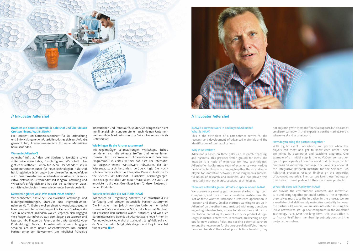
INAM ist ein neues Netzwerk in Adlershof und über dessen Grenzen hinaus. Was ist INAM?
Hier entsteht ein Kompetenzzentrum für die ErforschungundEntwicklungneuerMaterialien,dasessichzurAufgabegemacht hat, Anwendungsgebiete für neue Materialienherauszufinden.
Warum in Adlershof?
Adlershof fußt auf den drei Säulen: Universitäre sowieaußeruniversitäre Lehre, Forschung und Wirtschaft. Hiergibt es fruchtbaren Boden für Ideen. Der Standort ist einKompetenzknotenpunkt für neue Technologien. AdlershofhatlangjährigeErfahrung–überdiverseTechnologiefelder– im Zusammenführen verschiedenster Akteure für inno-vativeNetzwerke.Erverbindetseit langemForschungundWirtschaft erfolgreich und hat das bei zahlreichen Quer-schnittstechnologienimmerwiederunterBeweisgestellt.
Netzwerke gibt es viele. Was macht INAM anders?
Wirbeobachten,dasseineLückezwischenForschungs-undBildungseinrichtungen, Start-ups und Hightech-Unter-nehmen klafft. Erstere wollen einen Anwendungsbezug inForschungundLehreeinbringen.FürkleinereStart-ups,diesich in Adlershof ansiedeln wollen, ergeben sich dagegenvieleFragenzur Infrastruktur,zumZugangzuLaborenundMesstechnik. Fragen zu Patentrechten, Markteintritt oderProduktdesign. Größere Industrieunternehmen hingegenschauen sich nach neuen Geschäftsfeldern um, suchenPartner unter den Newcomern, um möglichst frühzeitig
InnovationenundTrendsaufzuspüren.Siebringensichnichtnur finanziell ein, sondern stehen auch kleinen Unterneh-menmitihrerMarkterfahrungzurSeite.HiersetzenwiralsNetzwerkan.
Wie bringen Sie die Partner zusammen?
Mit regelmäßigen Veranstaltungen, Workshops, Pitches,bei denen sich die Akteure treffen und kennenlernenkönnen. Hinzu kommen auch Accelerator- und Coaching-Programme. Ein erstes Beispiel dafür ist der internatio-nal ausgeschriebene Wettbewerb AdMaCom, der denWissensaustausch besonders berücksichtigt. Die Hoch-schule–hiervorallemdasIntegrativeResearchInstituteforthe Sciences IRIS Adlershof – erarbeitet Forschungsergeb-nissezuEigenschaftenvonneuenMaterialien.DieStart-upsentwickelnaufdieserGrundlageIdeenfürderenNutzunginneuenProdukten.
Welche Rolle spielt die WISTA für INAM?
Wir stellen die Umgebung, Kontakte, die Infrastruktur zurVerfügung und bringen potenzielle Partner zusammen.Die Initiative muss jedoch von den Unternehmen selbstkommen.DabeisindwireinMittler,derbewusstNeutrali-tät zwischen den Partnern wahrt. Natürlich sind wir auchdaraninteressiert,überdasINAM-NetzwerkneueFirmenimTechnologieparkAdlershofanzusiedeln.LangfristigsollsichderVereinausdenMitgliedsbeiträgenundProjektenselbstfinanzieren. ah
// Inkubator Adlershof
INAM is a new network in and beyond Adlershof. What is INAM?
This is the birthplace of a competence centre for theresearch and development of advanced materials and theidentificationoftheirapplications.
Why in Adlershof?
Adlershof is based on three pillars, i.e. research, teaching,and business. This provides fertile ground for ideas. Thelocation is a node of expertise for new technologies.Adlershofembodiesmanyyearsofexperience–overvariousfieldsoftechnology–inbringingtogetherthemostdiverseplayersforinnovativenetworks.Ithaslongbeenasuccess-ful union of research and business, and has proven thisrepeatedlywithothercrosssectionaltechnologies.
There are networks galore. What’s so special about INAM?
We observe a yawning gap between startups, high techcompanies,andresearchandeducational institutions.Thelast of these want to introduce a reference application inresearchandtheory.SmallerstartupswantingtosetupinAdlershof,ontheotherhand,arefacedwithmanyquestionsregarding infrastructure,accessto laboratoriesand instru-mentation, patent rights, market entry, or product design.Largerindustrialenterprises,incontrast,arekeepinganeyeoutfornewbusinessfieldsandseekingpotentialpartnersamongthenewcomersforthepurposeofidentifyinginnova-tionsandtrendsattheearliestpossibletime.Inreturn,they
notonlybringwiththemthefinancialsupport,butalsoassistsmallcompanieswiththeirexperienceonthemarket.Hereiswherewestandasanetwork.
How do you bring the partners together?
With regular events, workshops, and pitches where theplayers can meet and get to know each other. Theseare joined by accelerator and coaching programs. Oneexample of an initial step is the AdMaCom competitionopentoparticipantsallovertheworldthatplacesparticularemphasisonknowledgeexchange.Theuniversity,aboveallthe Integrative Research Institute for the Sciences IRISAdlershof, processes research findings on the propertiesofadvancedmaterials.Thestartupstakethesefindingsastheirbasistodevelopideasfortheiruseinnewproducts.
What role does WISTA play for INAM?
We provide the environment, contacts, and infrastruc-tureandbringtogetherpotentialpartners.Thecompaniesthemselvesmusttaketheinitiative. Intheprocess,weareamediatorthatdeliberatelymaintainsneutralitybetweenthepartners.Ofcourse,wearealsointerestedinusingtheINAM network to set up new companies in the AdlershofTechnology Park. Over the long term, this association isto finance itself from membership subscriptions and theprojectsthemselves.
// Incubator Adlershof
Adlershof special 466 Adlershof special 46 7

Ein Leuchtturm für neue MaterialienDas neu gegründete INAM-Netzwerk will brillante Ideen in die Praxis überführen – hin zu marktreifen Produkten in Elektronik, Optik und Photonik.
A recent setup, the INAM network intends to intro-duce brilliant ideas to the field – and to marketable products in electronics, optics, and photonics.
OhneGrundlagenforschungkeineneuenMaterialien.DochallzuoftbleibenbahnbrechendeErkenntnisse indenLabors stecken, weil Wissenschaftler den Schritt zum Pro-dukt scheuen. Es ist wichtig, dass alle Akteure im ProzessvonderIdeezurvermarktbarenInnovationaneinemStrangziehen.DeshalbhabensichimWissenschafts-undTechnolo-gieparkBerlin-AdlershofunlängstForscherundVertreterderWirtschaft zum Innovationsnetzwerk für neue Materialien(InnovationNetworkforAdvancedMaterials,INAM)zusam-mengeschlossen.
„Ziel istes, innovativeKonzeptezumEinsatzneuerMateri-alien und Technologien in Elektronik, Optik und Photonikzu entwickeln und umzusetzen“, erklärt INAM-Interims-vorstand Nikolai Puhlmann. Dabei handelt es sich zumBeispiel um kostengünstige Produktionsprozesse dankneuer Drucktechnologien, transparente, leitfähige Be-schichtungen für Dünnschichtsolarzellen oder die Weiter-entwicklung organischer Leuchtdioden (OLED) für dieAutomobilbranche.„Besonderswichtigistunsdabei,Grund-lagenforschung und Anwendung so weit wie möglichzusammenzubringen“,betontPuhlmann.
Entsprechend finden sich im INAM Partner entlang dergesamtenWertschöpfungskette,unteranderemdieOSRAMGmbH, die Ledvance GmbH, das Integrative ResearchInstitute for the Sciences (IRIS Adlershof) der Humboldt-Universität zu Berlin, die WirtschaftsfördergesellschaftBerlin Partner und die WISTA-MANAGEMENT GMBH. DieKompetenzensindbreitgefächert:DasSpektrumweitererNetzwerkerreichtvonderaufProduktdesignspezialisiertenAgenturPilotfishGmbHüberdieoffeneEntwicklungswerk-statt Fab Lab Berlin bis zur Patent- und Technologietrans-ferberatung durch die Humboldt-Innovation GmbH sowieWeitnauerRechtsanwältePartnerschaftsgesellschaft.
InitiiertwurdedaszunächstaufdreiJahreangelegteNetz-werkvonVordenkernausAdlershofundBerlinPartner.Daskommt nicht von ungefähr, denn in Adlershof haben rundumdasIRISetlicheaußeruniversitäreForschungseinrichtun-gen und innovative Unternehmen ein Kompetenzzentrumder optischen Analytik und der Materialwissenschaftenentstehenlassen. mh
A beacon for advanced materials
INAM-Interimsvorstand Nikolai Puhlmann (r.) und INAM-Geschäftsführer Jonas Pauly vor einem Plan des IRIS-Forschungsneubaus.
Nikolai Puhlmann (right), interim INAM chair and INAM CEO Jonas Pauly in front of a visualisation of the new IRIS research building. Nobasicresearch,noadvancedmaterials.Yetalltoo
often,pioneeringknowledgefailstoleavethelaboratorybe-causescientistsshunthesteptotheproduct.Itisimportantthat all players join forces in the process from the idea tothemarketableinnovation.Forthisreason,researchersandindustryrepresentativesrecentlycametogether intheAd-lershofScienceandTechnologyParktotakepartintheInno-vationNetworkforAdvancedMaterials(INAM).
“Theobjectiveistodevelopandrealiseinnovativeconceptsfortheapplicationofadvancedmaterialsandtechnologies
in electronics, optics, and photonics,” explained NikolaiPuhlmann,interimINAMchair.Theseinclude,forexample,newprintingtechnologiesforreducingproductionprocesscosts,transparent,electricallyconductingcoatingsforthin-filmsolarcells,andthefurtherdevelopmentoforganiclightemittingdiodes(OLEDs)fortheautomotivesector.“Wefindit particularly important to combine basic research andapplication to the maximum possible extent,” stressedPuhlmann.
Accordingly,theINAMpartnersalongtheentirevaluechaininclude OSRAM GmbH, Ledvance GmbH, the IntegrativeResearch Institute for the Sciences (IRIS Adlershof) of HUBerlin, the business promoter Berlin Partner, and WISTA-MANAGEMENT GMBH. The expertise these embody pre-sentsitselfoverabroadfront:othernetworkusersarethespecialisedproductdesignagencyPilotfishGmbH,theopendevelopmentworkshopFabLabBerlin,andpatentandtech-nologytransferconsultantsatHumboldt-InnovationGmbHandWeitnauerRechtsanwältePartnerschaftsgesellschaft.
Initiallyconceivedforthreeyears, thenetworkwas initiat-edbyguidingintellectualforcesfromAdlershofandBerlinPartner. This should not come as a surprise. After all, themany non-university research institutes and innovativecompaniesnestledaroundtheIRISinAdlershofhavegivenrise to a competence centre for optical analytics andmaterialsciences.
Adlershof special 468 Adlershof special 46 9

„Wir arbeiten daran, Eigenschaften klassischerHalbleitermaterialienmitdenjenigenvonneuartigenWerk-stoffen zu kombinieren“, sagt Professor Rabe. Aussichts-reiche Kandidaten sind zweidimensionale Materialienwie das Graphen. Die aus einer ultradünnen Schicht vonKohlenstoffatomen bestehende anorganische SubstanzleitetStrom, istextremreißfestundzugleichdehnbar.DasMaterial lässt sich großflächig mit organischen Stoffen –MolekülenundPolymeren–mischen.DerEinbauvonStick-stoffatomen verleiht Halbleitereigenschaften. Die Herstel-lung eines solchen Kohlenstoffnitrids gelang vor kurzemerstmalseinerGruppeumRabe.
„Wir wollen die kurzen Wege in Adlershof nutzen und zu-demneuePlayerherholen“, sagtRabe.Dazuwirdauchderangrenzende Forschungsneubau beitragen, der bis 2018
”Our work involves combining the properties ofclassical semiconductors with those of advanced materi-als,”explainedprofessorRabe.Highlypromisingcandidatesare2Dmaterialslikegraphenes.Consistingofanultrathinsheet of carbon atoms, this inorganic substance conductselectricity, is extremely resistant to tearing, and is alsoelastic. The material can be mixed over a large area withorganic substances – molecules and polymers. Integratingnitrogen atoms lends the substance semiconductor prop-erties. Recently, a group headed by Rabe was the first tomanufacturethiscarbonnitride.
“WeintendtoutilisetheshortpathsinAdlershofandalsofetch new players on board,” claimed Rabe. Contributionswillalsobesuppliedbythenew,adjoiningresearchbuildingwhosecompletionisplannedfor2018.Approximately4500
Was sollen die neuen Materialien können, die die zukünftige Elektronik dringend benötigt? „Schneller, heller, effizienter – und vor allem multifunktionaler sollen sie sein“, sagt Jürgen P. Rabe, Professor am Institut für Physik der Humboldt-Universität zu Berlin und Sprecher von IRIS (Integrative Research Institute for the Sciences) Adlershof. Mit Silizium, dem traditionellen Werkstoff der Halbleitertechnologie, alleine sind diese Eigenschaften schwer zu erreichen. Es gelte, neue Stoffe zu finden, die beispielsweise leitfähig und trotzdem transparent, großflächig und zudem flexibel seien. Dieser Herausforderung stellt sich das 2009 gegründete, derzeit rund 100 Mitarbeiter starke Institut mit seinem Forschungsfeld „Hybridsysteme für Optik und Elektronik“.
What are the advanced materials supposed to have that the electronics of the future so desperately needs? “More speed, more brightness, more performance – and above all more multifunctionality,” replied Jürgen Rabe, Physics Professor at the Humboldt-Universität zu Berlin and chairman of IRIS (Integrative Research Institute for the Sciences) Adlershof. Silicon alone, the traditional material of semiconductor technology, can help to achieve these properties only with great difficulty. New substances must now be found that, for example, are electrically conducting, yet transparent, exhibit large areas, and yet are flexible. Set up in 2009 and now employing a workforce of about 100, the institute specialising in hybrid systems for optics and electronics took up this challenge.
Das Beste aus zwei Welten// The best of both worlds
fertig sein soll. Auf rund 4.500 Quadratmetern werdenetwa 140 Wissenschaftler Platz finden und sich der inter-disziplinären Forschung an den anorganisch-organischenHybridmaterialienwidmen:Chemiker,PhysikeroderMateri-alwissenschaftler–auchTheoretiker,diefürdieBerechnunggroßerMoleküleandenGrenzflächenunverzichtbarsind.
Rabe sieht die Aufgabe des Teams auch darin, Synergienzu schaffen zwischen dem Verständnis der wissenschaft-lichen Grundlagen und der technischen Anwendung inneuenProdukten.DazudientderKontaktzuStart-upsundzu etablierten Unternehmen, die neue Geschäftszweigeaufbauen,sowiedieKooperationmitstrategischenPartnernauchaufnationalerundinternationalerEbene.Sowundertes nicht, dass IRIS einer der federführenden Partner imneuenMaterialien-NetzwerkINAMist. pj
square metres will provide the workspace for about 140scientists dedicated to interdisciplinary research intoorganic-inorganic hybrid materials. These will includechemists,physicists,materialscientists,andeventheoristswhoareindispensableforthecalculationsinvolvingmacro-moleculesattheboundarysurfaces.
Rabe also sees his team’s tasks in generating synergiesbetweentheunderstandingofscientificprinciplesandtheirtechnical application in new products. This is helped bycontacts with startups and established companies build-ing up new lines of business and by joint ventures withstrategic partners, also on the national and internationallevels. It thereforecomesasnosurprisethat IRIS isoneofthechiefpartnersonthenewmaterialnetworkINAM.
Im IRIS-Forschungsneubau werden auf 4.500 Quadratmetern 140 Wissenschaftler interdisziplinär forschen.
140 Scientists will work interdisciplinary at the new IRIS research facility with 4.500 square metres of lab and office space.
©N
ickl
&P
artn
erA
rch
itek
ten
AG
Adlershof special 4610 Adlershof special 46 11
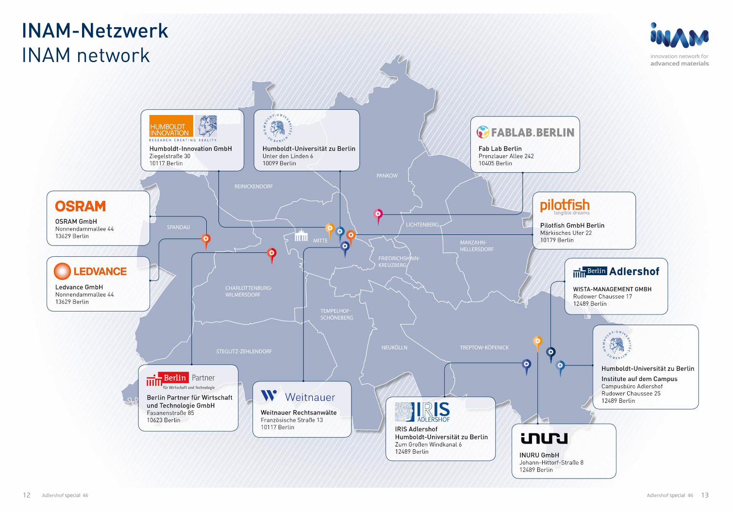
INAM-Netzwerk INAM network
Adlershof special 4612 Adlershof special 46 13

Von Mutigen, Machern und Mentoren
Of movers, makers, and mentors
Leuchtende Dioden, die so dünn sind, dass sie auf Papier und Verpackungen angebracht werden können bringen Aufdrucke oder Werbetexte zum Leuchten. Basis dieser und anderer neuer Produkte
ist die Forschung an neuen Materialien. Um Ergebnisse aus der Forschung schneller in die industrielle Praxis zu überführen, startete das Innovationsnetzwerk für neue Materialien in Berlin-Adlershof ein
Accelerator-Programm, für das sich Start-ups aus aller Welt bewarben.
LEDs, or light emitting diodes, that are so thin that they can be applied to paper and packaging supply the light for prints and slogans. These and
other new products are based on research into new materials. With a view to speeding up the transfer of research findings to the industrial field, the
Innovation Network for Advanced Materials (INAM) in Berlin-Adlershof launched an accelerator programme that received applications from
startups all over the world.
Praxisnahe Materialforschung: Was sich einfachanhört, hat viele Facetten. Um Ideen zu fördern, wurde inAdlershof Im Sommer 2016 mit dem „Advanced MaterialCompetition“ (AdMaCom) ein internationaler Wettbewerbfür Start-ups mit dem Schwerpunkt Hightechprodukteausgerufen. „Wir verbinden Forschung undWirtschaft undsuchen Start-ups mit marktnahen Produktideen, derenPotenzial wir gemeinsam ausloten.“ Bewerbungen für denWettbewerb“, freut sich Danny Krautz, Project ManagerPhotonics bei Berlin Partner, „kamen aus ganz Europa.“Interessenten gab es auch aus Brasilien und den USA.„Damit wollen wir auch erreichen, dass die Materialfor-schungamStandortAdlershofinternationalbessersichtbarwird“,erläutertderProjektmanagerweiter.KrautzwarselbstlangegenuginderMaterialforschungtätig,umzuwissen,dass die enge Zusammenarbeit von Forschung und Unter-nehmen eine wichtige Voraussetzung für die EntwicklungneuerProdukteist.
AdMaCom,einsechswöchigesProgramm,bringtTeamsausUnternehmen,Start-upsmitinnovativenIdeenundhohem
MarktpotenzialmitForschernundausgewählteninternati-onalen Mentoren zusammen. In Trainings und WorkshopserhaltendieTeamsundStart-upsBeratungaufdemWegzurEntwicklungneuer innovativerProdukteundVerfahren. ImLaufe des Sommers konnten die jungen Unternehmer mitExpertenausderIndustriediskutieren.Fünfzehnausgewähl-tenStart-upswerdenLaboreundMaterialienzurVerfügunggestellt,damitsieihreProdukteaufdienächsteStufehebenkönnen.BesondersamProgrammistauch,dassdieTeilneh-merkeine–wiesonstüblich inAccelerator-Programmen–Unternehmensanteile abtreten müssen sowie die Chanceerhalten,ihreIdeenaufführendenBranchenmessenwiederEOSAModerderMicrophotonics2016zupräsentieren.
Welche davon besonders vielversprechend sein werden,lässt sich heute noch nicht sagen. Das könnten Ideen ausder Displaytechnik sein, aus der Batterietechnik oder derPhotovoltaik. Auch neuartige Fasern oder Anwendungsbei-spielefürgedruckteElektroniksinddenkbar.„ImbestenFallerleben wir hier die Geburt ganz neuer Produkte“, hofftDannyKrautz. cl
Material research relevant to the field – Whatsoundssosimplepresentsawealthoffacets.Asameanstopromote ideas, the Advanced Material Competition(AdMaCom) was called into being in the summer of 2016in Adlershof, an international competition for startupsspecialising inhightechproducts.“Weuniteresearchandbusinessandareseekingstartupswithmarketableproductideaswhosepotentialweexplorejointly,”explainedDannyKrautz,PhotonicsProjectManageratBerlinPartner,contin-uing with obvious pleasure: “Applications for the compe-tition came from all over Europe.” Also Brazil and the USAwereamongtheinterestedparties.
“This isalso tohelpusachievebetternationalvisibilityofmaterialresearchattheAdlershoflocation,”heconcluded.Krautzhimselfhasspentmorethanenoughtimeinmaterialresearchtoknowthatclosecooperationbetweenresearchand industry is a key prerequisite for the development ofnewproducts.
ThesixweekprogrammeAdMaCombrings togethercom-panyandstartupteamsrepresentinginnovativeideasandgreat market potential with researchers and select inter-national mentors. Training courses and workshops offerthese teams and startups advice on their course towardsdeveloping new innovative products and processes. Overthe summer, young entrepreneurs can discuss their ideaswith experts from industry. Fifteen selected startups willbeprovidedwithlaboratoriesandmaterialstoelevatetheirproducts to the next level. Yet another special feature ofthisacceleratorprogramme,unlikeothersofitskind,isthattheparticipantsarenotcompelledtocedecompanysharesandaregiventheopportunitytopresenttheirideasatlead-ingexhibitionsinthesectorlikeEOSAMorMicrophotonics2016.
Which of these will prove especially promising cannot bepredictedtoday.Theycouldbeideasfordisplays,batteries,or photovoltaics. Also conceivable are innovative fibres orexampleapplicationsforprintableelectronics.“Intheidealcase,weshallexperiencethebirthofall-newproducts,”saidDannyKrautzwithhope.
Danny Krautz, Project Manager Photonics bei Berlin Partner, war selbst lange in der Materialforschung tätig.
Danny Krautz is Project Manager Photonics at Berlin Partner, and has himself worked in researching new materials for some time.
Ultraflache Beleuchtungsmodule von volatiles
Ultrathin lightening modules by volatiles
Adlershof special 4614 Adlershof special 46 15

Bei der Produktion von photovoltaischen Zellen oderLeuchtdioden werden im industriellen FertigungsprozessTemperaturenvonbiszu1.600GradCelsiuserreicht.WärendieTemperaturenniedriger,könntemanandieHerstellungvon flexiblen und großflächigen Anwendungen denken.„ErstTieftemperaturprozessevonhöchstens200GradCel-sius machen den Einsatz von flexiblen Substraten in denAnwendungenmöglich,etwaaufKunststoff-Folien“,erläu-tertEmilList-Kratochvil,ProfessorfürHybrideBauelementeanderHumboldt-UniversitätzuBerlin(HU).„DieFertigungwird energieeffizienter und damit auch kostengünstiger.ÜberdiessindsolcheProduktevielseitigereinsetzbar.“
List-Kratochvil wurde 2015 von der Technischen Universi-tät Graz und der NanoTechCenter (NTC) Weiz Forschungs-gesellschaftmbHandieHUberufen.EristeinsogenannterBrückenprofessor,seineProfessuristanzweiInstitutenan-gesiedelt:amInstitutfürPhysikundamInstitutfürChemie.Brückenprofessuren sollen Transferprozesse zwischen denDisziplinen unterstützen. Um die interdisziplinäre Erfor-schung von bislang unbekannten Eigenschaften hybriderMaterialienzustärken,wurdeeigensamCampusAdlershofdas Integrative Research Institute for the Sciences IRISgegründet,demauchList-Kratochvilangehört.
Brücken bauen
Building jointly
Wer die Materialien der Zukunft entwickeln will, muss interdisziplinär forschen. Dabei helfen Brückenprofessoren wie Emil List-Kratochvil und sein Kollege Norbert Koch.
Developing the materials of the future needs interdisciplinary research. This is provided by joint professorial appointments in the persons of Emil List-Kratochvil and his colleague Norbert Koch.
TheindustrialproductionofphotovoltaiccellsorLEDsrequires temperatures as high as 1600 degrees Celsius. Ifthesetemperatureswerelower,manufacturemightbecon-ceivedforflexibleapplicationsoverwideareas.“Theuseofflexiblesubstratesinapplicationsispossibleonlywhentheprocesstemperaturesarenohigherthan200°C,”explainedEmilList-Kratochvil,ProfessorofHybridComponentryattheHumboldt-UniversitätzuBerlin(HU).“Productionbecomesmoreenergyefficient,andthereforecostsless.Furthermore,theresultingproductshaveabroaderrangeofapplications.”
List-KratochvilwascalledtotheHUin2015fromtheGrazUniversityofTechnologyandtheresearchcompanyNano-TechCenter (NTC) Weiz Forschungsgesellschaft mbH. Heholds a so called joint professorial appointment, or chairsattwoinstitutes,herethePhysicsandChemistryInstitute.Jointprofessorialappointmentsaretosupportthetransferprocessesbetweenthedisciplines.Mandatedtopromotein-terdisciplinaryresearchintopreviouslyunknownpropertiesofhybridmaterials,theIntegrativeResearchInstitutefortheSciencesIRISAdlershofwassetupspecificallyontheAdlers-hofCampuswhosemembersalsoincludeList-Kratochvil.
Inthematerialsciences,interdisciplinaryexpertiseisthebe-allandend-all.“Specificallywhendealingwithelectroactivehybrid materials, scientists find it helpful to understandthe terminology used by the other discipline,” explainedList-Kratochvil. “And, in this manner, by expanding theirskillsintwodisciplines,studentsalsofindthedooropentogreaterprofessionalflexibility.”
HiscolleagueNorbertKoch–likewisewithajointprofessor-ialappointmentattheHUandamemberofIRISAdlershof–isalsoanativeAustrianlikeList-Kratochvilhimself.Kochstudied in Graz and then conducted research at PrincetonUniversitybeforereturningtoBerlinin2003.Thisprofessorofstructure,dynamics,andelectronicpropertiesofmolec-ularsystemsisfascinatedbymolecularelectronics.Behindthis istheideaofrealisingonedaytheoperationsofelec-troniccomponentswithsingleorasmallnumberofmole-culesengaginginspecificinteractions.
Kochisdedicatedtoboundarysurfaces,orverythinmaterialstructuresinthenanometreor,atmost,micrometrerange.Externalinfluenceslikeair,temperature,orhumidityinducehugechangesintheelectricalpropertiesofthesesensitivematerials. The scientist first investigates their propertiesin vacuum. “Then we change the ambient influences andobserve how the properties change,” explained Koch. Thegoalistooptimiseprocessesintheproductionofthinfilmmodulesandenhancetheirefficiency.Thiscan,forexample,reduce the costs even further of providing solar energy infuture.
Brückenbauer: Norbert Koch ist Professor für Struktur, Dynamik und elektronische Eigenschaften molekularer Systeme und fasziniert von der molekularen Elektronik.
Bridgebuilder: Norbert Koch is professor of structure, dynamics, and electronic properties of molecular systems and fascinated by molecular electronics.
untersucht er deren Eigenschaften zunächst im Vakuum.„Dann verändern wir die Einflüsse der Umgebung undbeobachten, wie sich die Eigenschaften verändern“, erläu-tertKoch.Ziel:ProzesseinderFertigungvonDünnschicht-modulen zu optimieren und effizienter zu machen. Damitkann zum Beispiel die Bereitstellung von Solarenergie inZukunftnochweitauskostengünstigerwerden. mh
Will Brücken bauen: Emil List-Kratochvil ist Professor für Hybride Bauelemente an der
Humboldt-Universität zu Berlin (HU).
Attempts to build bridges: Emil List-Kratochvil is Professor of Hybrid Componentry at
Humboldt-Universität zu Berlin (HU).
In den Materialwissenschaften sind fächerübergreifendeKenntnisse das A und O. „Besonders im Umgang mit elek-troaktiven hybriden Materialien ist es für Wissenschaftlerhilfreich,dieBegrifflichkeitenderjeweilsanderenDisziplinzuverstehen“,soList-Kratochvil.„StudierendeneröffnetsichmitderErweiterungihrerKenntnisseinzweiFächernzudemeinehoheberuflicheFlexibilität.“
Sein Kollege Norbert Koch – ebenfalls Brückenprofessoran der HU und Mitglied des IRIS Adlershof – stammt wieList-KratochvilausÖsterreich.KochhatinGrazstudiertunddanachanderPrincetonUniversitygeforscht.Erkambereits2003nachBerlin.DenProfessorfürStruktur,DynamikundelektronischeEigenschaftenmolekularerSystemefasziniertdie molekulare Elektronik. Dahinter steckt die Idee, dieFunktionvonelektronischenBauteileneinesTagesmithilfevoneinzelnenodernurwenigengezieltwechselwirkendenMolekülenzurealisieren.
Koch widmet sich den Grenzflächen, sehr dünnen Materi-alstrukturen imNano-oderhöchstensMikrometerbereich.Äußere Einflüsse wie Luft, Temperatur und auch Feuch-tigkeit verändern die elektrischen Eigenschaften dieserempfindlichen Materialien immens. Als Wissenschaftler
Adlershof special 4616 Adlershof special 46 1716

Das Start-up Inuru bringt Papier zum Leben, indem Licht und Animationen dank simpler Displays auf Papier gedruckt werden. Und das energieautark, umweltschonend und preisgünstig.
Wie gedruckte Bilder laufen lernen
Die Erfolgsstory beginnt imSushi-Laden. Patrick Barkowski undMarcin Ratajczak beugen sich überdie Speisekarte, überlegen, was manaus gedruckten asiatischen Zeichenund Bilderchen alles machen könnte.„Plötzlich hatten wir die Vision, dassdie kleinen Fische, die auf der Menu-karte aufgezeichnet waren, anfangenzuschwimmen.Unddanndachtenwir,daskannmandochwirklichmachen”,sagt Unternehmensgründer und Phy-siker Patrick Barkowski. Das nötigebetriebswirtschaftliche Know-howbrachte Marcin Ratajczak mit, der be-reits während seines Studiums unter-nehmerischeErfahrungensammelte.
Fasziniert von der OLED (organic lightemitting diode)-Technik startete ihreProjektidee 2012, im Jahr 2016 grün-deten die beiden die INURU GmbH.Mittels der OLED-Technik drucken sieAnimationen auf Papier und könnenso beispielsweise ein Printmagazin
This story of success beganin a sushi bar. While poring over themenu, Patrick Barkowski and MarcinRatajczakponderedallthethingstheycould do with printed Asian charac-ters and logograms. “Suddenly, wepictured the little fishes depicted onthemenustartingtoswim.Andthenwe thought that this could really be
The startup Inuru brings paper to life by printing it with light and animations on simple displays – a self sufficient, environmentally friendly, and low cost solution.
How printed images learned to swim
mitbewegtenBildernherstellen.„WirwollennichtnurindiePrintwerbung,sondern die OLEDs wirklich in denAlltag bringen. Jedes Magazin, jedeVerpackung kann mit Elektronik be-reichert werden”, sagt Barkowski, dersich schon während seines StudiumsauforganischeElektronikspezialisierthatte.GemeinsammitdemIndustrie-partnerOSRAMGmbHsindsie imIn-novationsnetzwerk INAM, um Poten-zialefürKosteneinsparungenzuevalu-ieren: „Wir versuchen den Preis nach-haltigzusenken, indemwirdieAuto-matisierungvonProzessbestandteilenevaluieren.”, sagt Thomas Waldmann,Leiter Energiemanagement Werk Ber-linSpandauderOSRAMGmbH.
Die Idee des OLED – ein leuchtendesDünnschichtbauelement aus organi-schen halbleitenden Materialien – istnicht neu. Bereits in den 1960er-Jah-ren gab es erste Forschungen. DieVorteile der OLEDs, im Gegensatz
zu anorganischen Leuchtdioden(LEDs),lagenfrühaufderHand:hoherKontrast, keine Hintergrundbeleuch-tung, geringer Stromverbrauch. DerNachteil: kurze Lebensdauer. InurustrebtmitseinenOLEDsbiszu10Wo-chenaktiveLeuchtzeitundeineLager-zeitvonübereinemJahran.
Mit ihrerFirmahabendiebeidenUn-ternehmensgründerheuteimTechno-logieparkAdlershofbestenAustauschmit Unternehmen, Wissenschaft undForschung.„Waswirentwickelthaben,isteinProzess,deraufgängigeDruck-maschinen transferiert werden kann”,sagt Barkowski. Dieser kann so anDruckereienausgelagertwerden.Kun-den müssen genau wissen, was beiihnen leuchten soll, dann übernimmtInuru die Einstellung der Druckpara-meter. Dieses Geheimnis haben diebeiden gelüftet, behalten es aber na-türlichgutgehütetfürsich. jg
done,” recounted founder and phys-icist Patrick Barkowski. The businessknowhowneededcameinthepersonofMarcinRatajczak,whoasastudenthad already gained entrepreneurialexperience.
FascinatedbytheOLED(organic lightemitting diode) technology, they
launchedtheirprojectideain2012,in2016bothfoundedtheINURUGmbH.UsingOLEDtechnology,theyprintani-mationsonpaper,makingpossible,forinstance, moving pictures in a print-edmagazine.“Wedidn’t justwant inprintedadvertising,butanactualinte-grationofOLEDsineverydayroutines.Every magazine, every item of pack-aging can be enriched withelectron-ics,” explained Barkowski, who hadspecialisedinorganicelectronicsevenbefore graduating from university.Togetherwiththeir industrialpartnerOSRAMGmbH,theyareamemberoftheinnovationnetworkINAMinordertoevaluatepotentialsforcost-saving.“Weareendeavouringtoreducecostssustainablybyevaluatingautomationofprocesscomponents,”saidThomasWaldmann, Energy Management Di-rector at the Berlin Spandau site ofOSRAMGmbH.
TheideabehindtheOLED,alight-emit-ting, thin-film component of organicsemiconducting materials, is not anewone.Initialresearchwasconduct-ed as early as the 1960s. Comparedwith inorganic LEDs, OLEDs offeredadvantagesthatwererecognisedear-lyon:highcontrast,nobacklight,lowpower consumption. The drawback,however,wastheshortservicelife.In-uruOLEDsaretoemit lightuptotenweeksandhaveashelflifeinexcessofmorethanoneyear.
By setting up their company in theAdlershof Technology Park, the twofounderstodayenjoythebestknowl-edge sharing contacts with compa-nies,science,andresearch.“Whatwehave developed is a process that canbe transferred to conventional press-es,” emphasised Barkowski. Custom-ers need only know what they wantto light up, and Inuru configures theprintingparameterswhichthencanbeapplied at any print shop.This secrethasrevealed itselftothetwofound-ers, who, of course, keep it closely tothemselves.
Marcin Ratajczak (links) und Patrick Barkowski von Inuru bringen Papier zum Leben.
Marcin Ratajczak (left) und Patrick Barkowski of start-up Inuru bring paper to life.
Adlershof special 4618 Adlershof special 46 19

In den Ozeanen sind Pilotfische nützliche BegleitergroßerMeeresbewohner,mitdenensieineinerArtSymbi-ose leben. Sie werden auch Lotsenfisch genannt. Im Inno-vationsnetzwerkfürneueMaterialienistdasUnternehmenPilotfishindieserRolledurchausrichtigverortet.
„WirhabenguteAntennen“,sagtMarcNagelüberseinVer-ständnisvonTechnikentwicklungundNetworkingund„wirschauengerninunterschiedlicheKüchen“.EristGründungs-partnerbeiPilotfish,einemimJahr2000entstandenenUn-ternehmen,dassichmitstrategischemDesignundmitderEntwicklungintelligenterProduktebefasst.AusgangspunkteseieninderRegeldieVorstellungenderKunden,diePilotfishbeauftragen,ihre„IdeenineinProduktzuüberführen“.
Patentanwälte, ein fabelhaftes Laboratorium und Lotsenfische: Im Innovations- netzwerk für neue Materialien (INAM) geht es auch um das Wissen um das Wissen herum. Das stellen eine Menge kompetenter Partner zur Verfügung.
Networking von der Forschung bis zur Vermarktung
Neben einem breiten Instrumentarium interdisziplinä-rer Methoden sei es vor allem der andere Blickwinkel unddie Freiheit, anders zu denken, als es aus Binnensicht derKundenmöglichwäre.Pilotfishistwieselbstverständlichinvielen unterschiedlichen Marktbereichen unterwegs, vonder Mobilität, der Medizintechnik bis zur Kommunikation,„unsere Aufträge erstrecken sich von Entwürfen bis zumPrototypenbauundderVermarktung.
InzwischenstehenvielfachneueMaterialienunddieFrage,wasmandarausmachenkönne,amAnfanginnovativerPro-duktentwicklung. „Wir beschäftigen uns schon seit JahrenmitMaterialwissenschaften“,erläutertNagel,undnenntalsBeispiele„intelligenteMaterialienbeiSport-oderAlltagsbe-kleidung,diemehralsnureineHüllefürdenNutzerabgebenkönnen“. Um denWeg von derForschung über dieUmset-zunginProduktebiszurMarktreifegeradebeineuenMate-rialien inElektronik,OptikundPhotonikmitbeschreitenzukönnen, habe sich Pilotfish an der Gründung des Innovati-onsnetzwerkesINAMimJuni2016inAdlershofbeteiligt.
Auch das FabLab in Berlin-Mitte gehört zum INAM-Netz-werk. Es ist eine offene Entwicklungswerkstatt, die nachdemVorbilddesBostonerMITjungenEntwicklernundStu-dierendeneinenfreienZugangzuHightechwerkzeugener-öffnet.HierstehenauchIndustriepartnerwieOttoBockoderMakea Industries den Kreativen zur Seite, um den EinstiegindieNutzunginnovativerTechnologienzuermöglichen.FürdasBerlinerBürovonPilotfishistdieZusammenarbeitmitdemFabLab,etwabeimPrototypenbau,eineselbstverständ-licheKooperationimNetzwerk.
AberINAMverknüpftnichtnurWissenschaftundWirtschaft,ForschungundEntwicklung.IhmgehörtzudemalsPartnerdie Weitnauer Rechtsanwälte Partnerschaftsgesellschaftan,dieihrWissenimUmgangmitdenrechtlichenAspektengeistigenEigentumseinbringt.„Esistsinnvoll,sichfrühzei-tigüberdierechtlichenBedingungenzuunterhalten“,sagtSvenSchilf,LeiterderPraxisgruppeIntellectualPropertybeiWeitnauer, „idealerweise schon bei der Konzeptionierungeines Projektes“. Denn das sichert den Erfolg beim Schutzund der erfolgreichenVerwertung der Ideen, gewerblichenSchutzrechteundgeistigenSchöpfungenderUnternehmen.
ko
BOARDINGHAUS
ANZEIGE|ADVERTISEMENT
Intheworld’soceans,pilotfisharetheusefulescortsof large sea dwellers with which they live in a kind ofsymbiosis.So the InnovationNetwork forAdvancedMate-rialsistherightplacefortheroleadoptedbythecompanyPilotfish.
Patent agents, a fabulous laboratory, and Pilotfish: The Innovation Network for Advanced Materials (INAM) is constantly focused on the knowledge leading to and from knowledge. And this is provided by a lot of competent partners.
Networking from research to marketing
Marc Nagel Geschäftsführer von Pilotfish
Marc Nagel CEO of Pilotfish
Adlershof special 46 21Adlershof special 4620

/ ADLERSHOF IN ZAHLEN / ADLERSHOF IN FIGURES(Stand: 1.1.2016) (As at: 1.1.2016)
STADT FÜR WISSENSCHAFT, TECHNOLOGIE UND MEDIENFläche: 4,2 km² Beschäftigte: 15.996 Unternehmen und Institute: 1.013
WISSENSCHAFTS- UNDTECHNOLOGIEPARKUnternehmen: 510 Mitarbeiter: 6.134 Außeruniversitäre Forschungseinrichtungen: 10Mitarbeiter: 1.680
HUMBOLDT-UNIVERSITÄT ZU BERLINNaturwissenschaftliche Institute: 7
Mitarbeiter: 1.055 Studierende: 6.524
MEDIENSTADTUnternehmen: 140Mitarbeiter: 1.977 (inkl. freier Mitarbeiter)
GEWERBEUnternehmen: 363 Mitarbeiter: 5.150
LANDSCHAFTSPARKFläche: 66 ha
CITY OF SCIENCE, TECHNOLOGY AND MEDIAArea: 4.2 km² (1,038 acres) Staff: 15,996 Companies and Institutes: 1,013
SCIENCE AND TECHNOLOGY PARKCompanies: 510Employees: 6,134Non-university research institutes: 10Employees: 1,680
HUMBOLDT-UNIVERSITÄT ZU BERLIN Science departments: 7 (IRIS Adlershof, Institutes of Chemistry, Geography, Computer Sciences, Mathematics, Physics and Psychology)
Employees: 1,055 Students: 6,524
MEDIA CITYCompanies: 140Employees: 1,977 (including freelancers)
COMMERCIAL AREACompanies: 363 Employees: 5,150
LANDSCAPE PARKLANDArea: 66 ha
(IRIS Adlershof, Institute für Chemie, Geographie, Informatik, Mathematik, Physik und Psychologie)
// Networking from research to marketing
“Wehaveagoodnose,”explainedMarcNagelwhenaskedto reveal how he understands technological progress andnetworking,“andweliketotakea lookinmanykitchens.”HeisthefoundingpartnerofPilotfish,a2YKsetupspecial-isinginstrategicdesignandthedevelopmentofintelligentproducts.HeexplainedthatthestartingpointsaregenerallytheideasofcustomerswhocommissionPilotfishto“trans-latetheirideasintoaproduct”.
Inadditiontoawideportfolioofinterdisciplinarymethods,the key driving force is the different angle of view andthe freedom to think differently than possible within thecustomer’sownisland.Asamatterofcourse,Pilotfishtra-versesmanydifferentmarketsegments,includingmobility,
medical engineering, and communication: “Our assign-ments cover the whole range of drafts, prototyping, andmarketing.”
In the meantime, there are many advanced materials atthe beginning of innovative product development, andthequestionofwhatcanbedonewiththem.“We’vebeenbusying ourselves with material sciences for years,” ex-plainedNagel,namingasexamples“intelligentmaterialsinsports and everyday clothing that can serve as more thanjustacoveringfortheuser”.Toprepareitscoursealongthepathfromproductresearchto implementationtomarket-ability, specifically with respect to advanced materials inelectronics, optics, and photonics, Pilotfish collaborated inthesetupoftheinnovationnetworkINAMinJune2016inAdlershof.
AlsotheFabLabinBerlinMitteisamemberoftheINAMnet-work.Thisisanopendevelopmentworkshopthat,followingtheexampleoftheBostonMIT,providesyoungdevelopersandstudentswithfreeaccesstohightechtools.Here,crea-tivemindsalsofindsupportinindustrialpartnerslikeOttoBock or Makea Industries, and easier entry into the use ofinnovativetechnologies.ForthePilotfishofficeinBerlin,thecollaborationwithFabLab,e.g.inprototyping,isamatterofcourseonthenetwork.
Yet INAM not only links science and business, researchand development. Its partners also include theWeitnauerRechtsanwälte Partnerschaftsgesellschaft that contributesits knowledge of legal aspects involved in intellectualproperty. “It makes sense to discuss the legal conditionsin advance,” said Sven Schilf, Director of the IntellectualProperty Practice Group at Weitnauer. “Ideally as early asthe project’s conception phase.”This alone safeguards theprotection and successful utilisation of ideas, industrialpropertyrights,andthecompanies’intellectualworks.
Reges Treiben im Schulungsraum im FabLab.
Hustle and bustle at the FabLab-lecture room.
Adlershof special 46 23Adlershof special 4622

intelligente lösungen für ihre energieversorgung. Lösungen für die Energieversorgung von morgen entwickeln. Das ist unser Anspruch. Und dafür steht unser Heizkraftwerk Adlershof:
> Mit hocheffizienten Blockheizkraftwerken erzeugen wir Strom und Heizwärme
> Unsere Power-to-Heat-Anlagen nutzen Überschussstrom zur Erzeugung von Wärme
> Unsere Heißwasserspeicher schaffen Flexibilitäten und stellen eine unterbrechungsfreie Fernwärmeversorgung sicher
Das passt zu Adlershof. Das passt zu Berlin. Und das passt zu Deutschland als Land der Energiewende.
Mehr Informationen finden Sie unter
www.btb-berlin.de