in uence of patterned cu roughness on cu-emc … uence of patterned cu roughness on cu-emc interface...
TRANSCRIPT
Influence of Patterned Cu Roughness onCu-EMC Interface Adhesion Properties
Kaipeng HuMT 11.44
Internship report
Supervisors:dr.ir. Olaf van der Sluis (TU/e, Philips Research)ir. Sander Noijen (Philips Research)
Eindhoven University of TechnologyDepartment of Mechanical EngineeringDivision of Computational and Experimental MechanicsSection Mechanics of Materials
November , 2011, Eindhoven

Contents
Abstract i
1 Introduction 1
2 Theoretical Background 3
2.1 Cu-EMC Interface . . . . . . . . . . . . . . . . . . . . . . . . . . . . . . . . . 3
2.2 Interface Fracture Mechanics . . . . . . . . . . . . . . . . . . . . . . . . . . . 3
2.3 Crack Kinking Theory . . . . . . . . . . . . . . . . . . . . . . . . . . . . . . . 5
2.4 Adhesion Measurement Techniques . . . . . . . . . . . . . . . . . . . . . . . . 6
3 Experimental Analysis 8
3.1 Sample Preparation . . . . . . . . . . . . . . . . . . . . . . . . . . . . . . . . 8
3.2 Four-point Bending Test . . . . . . . . . . . . . . . . . . . . . . . . . . . . . . 10
3.3 Failure Surface Investigation . . . . . . . . . . . . . . . . . . . . . . . . . . . . 11
3.4 Cross-section Investigation . . . . . . . . . . . . . . . . . . . . . . . . . . . . . 12
3.5 Numerical Model . . . . . . . . . . . . . . . . . . . . . . . . . . . . . . . . . . 13
4 Results and Analysis 15
4.1 Load-displacement Curve . . . . . . . . . . . . . . . . . . . . . . . . . . . . . 15
4.2 Numerical Simulation Results . . . . . . . . . . . . . . . . . . . . . . . . . . . 18
4.3 Surface Morphology . . . . . . . . . . . . . . . . . . . . . . . . . . . . . . . . 20
4.4 Failure Surface SEM Images . . . . . . . . . . . . . . . . . . . . . . . . . . . . 23
4.5 Cross-section SEM Images . . . . . . . . . . . . . . . . . . . . . . . . . . . . . 24
5 Conclusions and Recommendations 27
5.1 Conclusions . . . . . . . . . . . . . . . . . . . . . . . . . . . . . . . . . . . . . 27
5.2 Recommendations . . . . . . . . . . . . . . . . . . . . . . . . . . . . . . . . . 28
Bibliography 29
Acknowledgements 31
i
Abstract
Debonding of polymer-metal interfaces is one of the main failure modes observed in micro-electronic components, which implies the adhesion at the interface is not sufficiently high.Surface roughening is one generally accepted way to enhance interface adhesion. One of thekey mechanisms, besides the obvious increase in surface area and mechanical interlocking, isthe transition from adhesive to cohesive failure, i.e. crack kinking. In this report an adhesionpromotion method for Copper-Epoxy Moulding Compound (Cu-EMC) interfaces via simpli-fied 2D microscopic groove-patterned roughness on the copper substrate is demonstrated.The focus is to obtain reproducible crack kinking, assess the relevant failure mechanisms andinvestigate the influence of surface roughness on Cu-EMC interface adhesion properties. Thespecimens used in the experimental study are made of Cu-EMC bimaterial strips. Specialpatterns composed of oriented parallel grooves of varying widths are etched on the coppersubstrate surface. The specimens are debonded by means of the four-point bending test. Atfirst, an estimate of the interface fracture toughness is extracted from the load-displacementcurves using an analytical solution. Subsequently, simulations with cohesive zone elements atthe interface are performed to evaluate the interface fracture toughness with the considera-tion of large strain, plastic deformation and friction. Several unusual features of experimentalload-displacement curves are explained with the aid of simulation results. The failure sur-face and cross-section of copper substrate are investigated under both optical microscopeand scanning electron microscope (SEM). A detailed morphology of the copper leadframe isdeduced and the kinking fraction is calculated.

Chapter 1
Introduction
With continuous reduction of circuit sizes, the reliability and durability of polymer-metalinterface is a significant concern in microelectronic industry. It has been found that delam-ination of two material layers is a key failure mechanism of the polymer-metal interface [1].Thus, during the past twenty years, considerable attention has been paid aiming at under-standing of this failure mode. This includes analytical [2], experimental [3–5], and numericalstudies [6–8].
The occurrence of delamination depends on debonding driving forces, such as intrinsic residualstress, thermal stress and external loading, and interface fracture toughness which can becharacterized by critical energy release rate (CERR) Gc. Therefore, reducing debondingdriving forces and increasing the interface fracture toughness are two strategies to improve theinterface reliability. This work focuses on the latter manipulation and elaborates an interfacefracture toughness promotion method by utilization of patterned surface roughness. Althoughthis a generally accepted method to enhance adhesion [9], quantitative understanding is stilllacking.
In order to improve the interface fracture toughness, the mechanisms of adhesion and cohesionshould be understood. The following interactions at various length scales play a role inadhesion and cohesion of materials and interfaces [7].
1. Chemical interactions: Chemical interactions inside materials and between materialsurfaces refer to primary bonds, i.e. covalent, ionic or metallic bonds. The interactionscale is about 0.2− 1.0 nm.
2. Physical interactions: Physical interactions refer to secondary bonds inside materialsand between interface, like the Coulomb force or Van der Waals force. Although ingeneral the magnitude of the physical interactions is weaker than the one of the primarybond, it is formed at most interfaces while chemical interactions are not met. Theinteraction scale is about 5.0− 10.0 nm.
3. Mechanical interlocking : Mechanical interlocking is the interactions between materialsurfaces or inside materials due to geometric effects at microscopic scale. The interlock-ing is considered to be the most significant mechanism in interface bonding. The scale
1
of surface roughness of metal-polymer interfaces, which is a typical interlocking feature,is in the order of micrometers.
When a crack impinges on the polymer-metal interface, it may either propagate along theinterface or deflect into the polymer. Thus, debonding of polymer-metal interface mightinvolve both adhesive and cohesive failure [8]. The cohesive failure refers to the situation inwhich the crack penetrates the polymer, which can be also called crack kinking [2]. Since thefracture toughness of the polymer is usually much greater than the polymer-metal interfacefracture toughness, it is desired to obtain more cohesive failure near the interface to promotethe interface fracture toughness. Kim et al. [10] employed micro-patterned surface topographyat polymer-metal surface and found that the roughness triggered mechanical interlockingprovides an energy dissipating process whereby viscoelastic and plastic energy dissipationand corresponding cohesive failure are required for crack propagation. Therefore, due to themechanical interlocking mechanism, increasing contact surface and crack kinking, roughenedsurfaces are used commonly in practice to obtain better interface fracture toughness.
In this report, a method of enhancing interface fracture toughness in a Cu-EMC bimate-rial strip through the introduction of well-defined roughness profiles at the copper leadframesurface is introduced. Various patterns composed of oriented parallel grooves are designedand etched on the copper leadframe surface prior to the EMC molding, aiming to form me-chanical interlocking, increase contact area and trigger crack kinking. The focus is to obtainreproducible crack kinking, assess the relevant failure mechanisms and investigate the influ-ence of surface roughness on Cu-EMC interface adhesion properties. Firstly, some theoreticalbackground knowledge such as interface fracture mechanics, interface description and Gcmeasurement techniques will be introduced in the forthcoming chapter. In Chapter 3 exper-imental procedures such as sample preparation, four-point bending test (4PB) and failuresurface investigation via both optical microscope and scanning electron microscope (SEM)will be demonstrated in detail. Additionally, a numerical model is introduced for a betterunderstanding of the experimental results. The results and analysis for load-displacementcurves, surface morphology, optical microscope and SEM images and numerical simulationswill be presented in Chapter 4. Finally, concluding remarks and recommendations will begiven in Chapter 5.
2
Chapter 2
Theoretical Background
2.1 Cu-EMC Interface
Due to its low cost, ease of processing, and excellent electrical properties, EMC becomesone of the most important materials used in encapsulation of the “System in Package” (SiP).However, the relatively high thermal expansion of epoxy induces thermal stress in the packageduring thermal cycling. Thus, inorganic fillers such as fused silica are used to lower thethermal expansion of EMC. Regarding the leadframes, copper-based alloys are currently themost widely used leadframe materials in microelectronic industry. It is ascribed to theirhigh thermal and electrical conductivities, and relatively low cost. Thus, the investigation ofCu-EMC surface has received a significant attention [11–14]. H. Y. Lee et al. [11] reportedthat chemical oxidation treatment of the copper-based leadframe before EMC molding couldpotentially increase the interface fracture toughness. However, another interface fracturetoughness promotion method, i.e. surface roughening will be discussed here.
2.2 Interface Fracture Mechanics
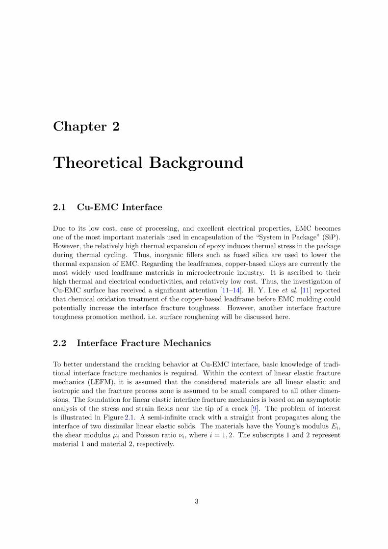
To better understand the cracking behavior at Cu-EMC interface, basic knowledge of tradi-tional interface fracture mechanics is required. Within the context of linear elastic fracturemechanics (LEFM), it is assumed that the considered materials are all linear elastic andisotropic and the fracture process zone is assumed to be small compared to all other dimen-sions. The foundation for linear elastic interface fracture mechanics is based on an asymptoticanalysis of the stress and strain fields near the tip of a crack [9]. The problem of interestis illustrated in Figure 2.1. A semi-infinite crack with a straight front propagates along theinterface of two dissimilar linear elastic solids. The materials have the Young’s modulus Ei,the shear modulus µi and Poisson ratio νi, where i = 1, 2. The subscripts 1 and 2 representmaterial 1 and material 2, respectively.
3
μ ,ν1 1
σ22
μ ,ν2 2
σ11
σ12
θ
x1
x2
rσ11
σ22
σ12
Figure 2.1: Stress state at the interfacial crack tip [9]
The material is subjected to static remote loading, and is assumed to deform in plane strain.Dundurs [15] introduced two elastic mismatch parameters
α =E1 − E2
E1 + E2
β =(1− 2ν2)/µ2 − (1− 2ν1)/µ12(1− ν2)/µ2 − 2(1− ν1)/µ1
, (2.1)
where Ei = Ei/(1 − νi2). Evidently α is a measure of the relative stiffness of the two
materials while β is a rough measure of the relative compressibility of the two materials [15].The condition α = β = 0 refers to a homogeneous condition.
For each material pair, a singular crack tip field exists at the crack tip according to linearelasticity theory. For problems considered here, the normal and shear stresses of the singularfield acting on the interface a distance r ahead of the tip can be written in a compact form
σ22 + iσ12 =(K1 + iK2)r
iε
√2πr
, (2.2)
where i ≡√−1 and the crack tip singularity parameter ε (also called mismatch parameter)
depends on β according to
ε =1
2πlog
(1− β1 + β
). (2.3)
For most of the bimaterials, the ε value is small and can be ignored. This leads to the fact thatthe amplitude factors K1 and K2 can be interpreted as Mode I and Mode II stress intensityfactors, respectively. They are defined to be consistent with corresponding stress intensityfactors, KI and KII , which are for cracks in homogeneous problems. It implies that they alsodepend linearly on the applied loads and the geometry. Thus, the energy release rate of thecrack in the interface is related to the interface stress intensity factor by
Gi =1
2 cosh2 πε
(1
E1
+1
E2
)(K2
1 +K22 ) (2.4)
Another important parameter representing the relative proportion of Mode I and Mode IIloading is the mode angle Ψ. For discussion purpose (as well as in many actual implementationcases), it is assumed that β = 0. Thus
4
Ψ = tan−1
(σ12σ22
)(2.5)
When Ψ = 0◦, it corresponds to pure mode I loading and Ψ = 90◦ corresponds to pure modeII loading.
2.3 Crack Kinking Theory
As mentioned before, debonding of bimaterials consists of adhesive and cohesive failures.He and Hutchinson [2] established an energy criterion to investigate the interface fracturetoughness promotion due to the surface roughness. From it, the conditions of the cohesivefailure, i.e. crack kinking, can be identified.
Given the fracture toughness of the interface Gic and that of the EMC Gec. The crack willpropagate along the interface if the condition Gi ≥ Gic is met. On the other hand, the crackwill deflect into the EMC if the energy release rate for the crack tip in the EMC, Ge, isgreater than Gec. Analogously, the crack will kink into the copper if Gc ≥ Gcc, where Gcc andGc are fracture toughness of copper and energy release rate for the crack tip in the copper,respectively. Since the fracture toughness of the copper Gcc is much higher than those of theinterface and the EMC, the possibility of deflection into the copper is relatively small and itwill not be considered here. In the case where an interface crack kinks out of the interfaceand into EMC the energy release rate Ge of the kinked crack may be determined from
Ge =1− ν1
2µ1(K2
I +K2II) (2.6)
Note that KI and KII are stress intensity factors of the kinking crack and are different fromthe interface stress intensity factors K1 and K2.
The energy release rate ratio GR is introduced in order to formulate the above discussion intoa mathematical form. The definition is as follows
GR =GiGe
(2.7)
Then the crack propagation path can be related to the energy release rate ratio GR in thefollowing way
GR =GiGe
>GicGec⇒ crack propagates along the interface (interface failure)
GR =GiGe
<GicGec⇒ crack deflects into the EMC (cohesive failure in EMC)
(2.8)
5
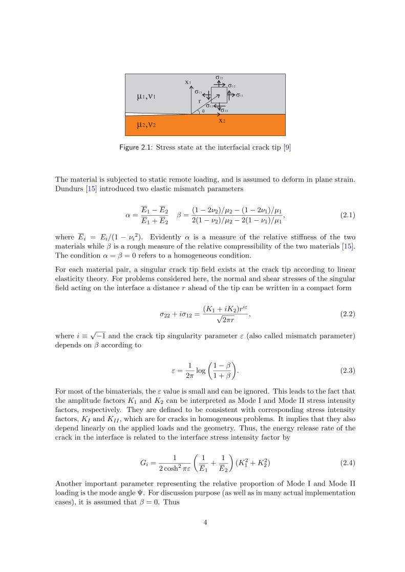
2.4 Adhesion Measurement Techniques
The CERR is dependent on the mode angle. Figure 2.2 present several basic configurationsfor adhesion measurement under different mode angles. The double cantilever beam (DCB)(a) and end notch flexure (ENF) (b) tests can induce pure Mode I and mode II delamination,respectively. The mode angle Ψ for 4PB test (d) is around 45◦ [4] but is dependent on thebulk materials and sample thickness. However, with the MMB test (c), a full range of modeangles can be obtained by alteration of the distance d between two external loads. In thisproject, configuration 4PB (d) test will be applied.
( ) ( ) ( ) ( )a b c d
p pd
Figure 2.2: Schematic of different loading angles for interface delamination:(a) DCB test;(b) ENF test; (c) mixed mode bending test; (d) 4PB test.
2
1h1
h2
h
b
P/2 P/2
Crack
LL Knife Edge
Pre-crack
(a) Schematic illustration
Displacement δ
Lo
ad P
initial slope
sudden drop
plateau
Pc
(b) Typical load-displacement curve
Figure 2.3: Schematic illustration of the 4PB setup (a) and the typical load-displacementcurve (b).
In Figure 2.3(a) the schematic illustration of 4PB test is presented. The external load is Pand the dimensions of the sample are also indicated. The sample is a layered bimaterial stripwith different materials 1 and 2. Initially, it contains a pre-crack. When the load reachesa critical value, the pre-crack will propagate perpendicularly towards the interface and growlongitudinally along the weakest interface or deflect into the bulk materials. The load isapplied to allow crack propagation to occur, and stops when the crack tip approaches theinner knife edges.
Figure 2.3(b) shows a typical load-displacement curve for a 4PB test. The initial slope of thiscurve represents the bending stiffness of the specimen. When the load reaches a certain value,
6
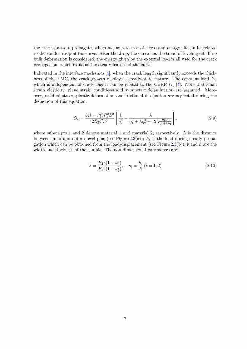
the crack starts to propagate, which means a release of stress and energy. It can be relatedto the sudden drop of the curve. After the drop, the curve has the trend of leveling off. If nobulk deformation is considered, the energy given by the external load is all used for the crackpropagation, which explains the steady feature of the curve.
Indicated in the interface mechanics [4], when the crack length significantly exceeds the thick-ness of the EMC, the crack growth displays a steady-state feature. The constant load Pc,which is independent of crack length can be related to the CERR Gc [4]. Note that smallstrain elasticity, plane strain conditions and symmetric delamination are assumed. More-over, residual stress, plastic deformation and frictional dissipation are neglected during thededuction of this equation,
Gc =3(1− ν22)P 2
c L2
2E2b2h3
[1
η32− λ
η31 + λη32 + 12λ η1η2η1+λη2
], (2.9)
where subscripts 1 and 2 denote material 1 and material 2, respectively. L is the distancebetween inner and outer dowel pins (see Figure 2.3(a)); Pc is the load during steady propa-gation which can be obtained from the load-displacement (see Figure 2.3(b)); b and h are thewidth and thickness of the sample. The non-dimensional parameters are:
λ =E2/(1− ν22)
E1/(1− ν21), ηi =
hih
(i = 1, 2) (2.10)
7

Chapter 3
Experimental Analysis
3.1 Sample Preparation
The Cu-EMC sample used in this project is shown in Figure 3.1. It is a layered bimaterialstrip. The top layer with the notation of “1” is EMC. It has a thickness of h1 = 0.5 mm orh1 = 1.0 mm. Two values are tried in order to trigger more delamination. While the bottomlayer, i.e. layer 2 is copper substrate with thickness of h2 = 0.2 mm. The length and widthare a = 48 mm and b = 8 mm, respectively.
In the partial enlarged view, the cross-section of the sample along y-direction is indicated.The grooves are created in the x-direction. It is assumed that there is no geometry variationin x-direction of the sample. Alternatively, all the cross-sections along the y-direction havethe same profiles. It is worth noting here that one reason for choosing this simplified 2Dgeometry is the consideration of quantitative validation of numerical models to prevent anyambiguities. In addition, the well-defined profiles make it easier for identification of failuremechanisms compared to the stochastically distributed 3D surface roughness.
2 Copper
1 EMCh1
h2
b
Etched Copper Surface
Pre-crack
y
x
z
a
h
Figure 3.1: Schematic of the Cu-EMC sample with pre-crack for 4PB test.
8
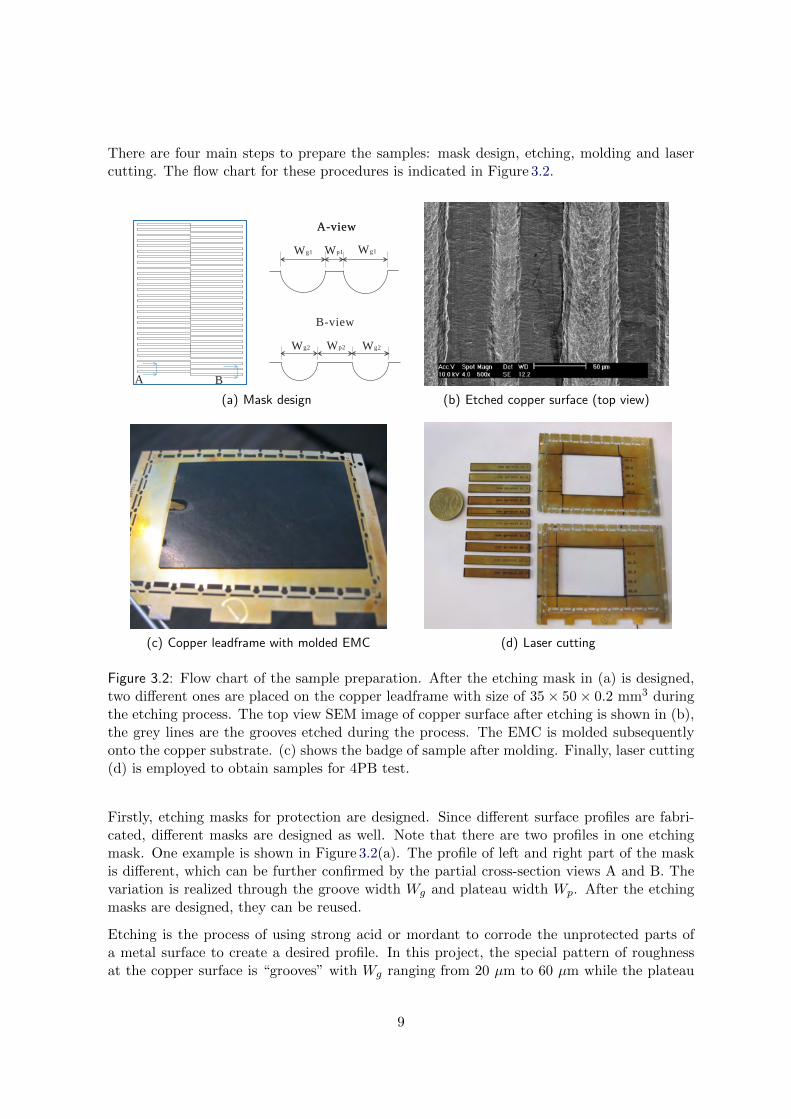
There are four main steps to prepare the samples: mask design, etching, molding and lasercutting. The flow chart for these procedures is indicated in Figure 3.2.
A-viewA-view
B-view
Wg1 Wg1Wp1
Wg2 Wg2Wp2
A B
(a) Mask design (b) Etched copper surface (top view)
(c) Copper leadframe with molded EMC (d) Laser cutting
Figure 3.2: Flow chart of the sample preparation. After the etching mask in (a) is designed,two different ones are placed on the copper leadframe with size of 35× 50× 0.2 mm3 duringthe etching process. The top view SEM image of copper surface after etching is shown in (b),the grey lines are the grooves etched during the process. The EMC is molded subsequentlyonto the copper substrate. (c) shows the badge of sample after molding. Finally, laser cutting(d) is employed to obtain samples for 4PB test.
Firstly, etching masks for protection are designed. Since different surface profiles are fabri-cated, different masks are designed as well. Note that there are two profiles in one etchingmask. One example is shown in Figure 3.2(a). The profile of left and right part of the maskis different, which can be further confirmed by the partial cross-section views A and B. Thevariation is realized through the groove width Wg and plateau width Wp. After the etchingmasks are designed, they can be reused.
Etching is the process of using strong acid or mordant to corrode the unprotected parts ofa metal surface to create a desired profile. In this project, the special pattern of roughnessat the copper surface is “grooves” with Wg ranging from 20 µm to 60 µm while the plateau
9

Figure 3.3: 4PB test setup
ranges also from 20 µm to 60 µm (see Figure 3.2(b)). Note that this picture is from the Set-1samples. The grooves are not semi-circular. But samples in Set-2 and Set-3 are better. Thecopper leadframe has a size of around 35× 50× 0.2 mm3 and two different etching masks areplaced on it in order to get four different profiles.
After the etching process, a layer of commercial black EMC with a thickness of 0.5 mmor 1.0 mm is molded on the copper leadframe. It is necessary to clean the copper surfacewith a sulphuric acid dip and plasma before molding in order to improve the conditions foradhesion. The molding process lasts 180 s with the temperature of 180 ◦C and the pressure of200 bar. The post mold cure takes 4 hours at 175◦ C. Thus, badges with typical dimensionsof 35 × 50 × 0.7 mm3 (when h1 = 0.5 mm) or 35 × 50 × 1.2 mm3 (when h1 = 1.0 mm) areobtained. The picture of the badge is shown in Figure 3.2(c).
Subsequently, four strips are laser cut from one badge. Finally, a pre-crack as shown inFigure 3.1 is made by laser cutting.
The following table shows the material properties of two materials.
Table 3.1: Material properties of the copper leadframe and EMC.
Young’s Modulus E (MPa) Poisson’s Ratio ν (-)
Material 1 (EMC) 21240 0.25
Material 2 (Cu) 123000 0.33
3.2 Four-point Bending Test
The interface fracture toughness, which is the critical energy release rate when fracture occurs,is measured by four-point bending test. A picture of the setup is presented in Figure 3.3. Thesamples are tested with a constant loading rate of 0.5 mm/min. The loads are measured witha resolution of 0.01 N and digitally recorded to generate the load-displacement curve. Thetest will be stopped when the crack approaches the inner knife edges (see Figure 2.3(a)). Alltests are conducted at room temperature.
10
During the experiment, three sets of samples, namely Set-1, Set-2 and Set-3, with differentsurface morphologies are tested. Additionally, the thickness of EMC in Set-1 and Set-2 is0.5 mm while in Set-3 it is 1.0 mm. Two samples in set-3 are glued with an additionalcopper layer. The alterations are intended to increase the stored energy in the bulk materialsand thus trigger more delamination, which can eventually increase the possibility of crackkinking. Except for two samples from Set-3, namely sample S1 and L1, all the samplesexhibit a delaminating interface. Thus, sample S1 and L1 are left out of the analysis. As willbe indicated in Section 4.3 samples in Set-1 show a small amount of crack kinking while Set-2samples barely have crack kinking and Set-3 samples display a large area of it. The reasonsfor this difference will be explained later.
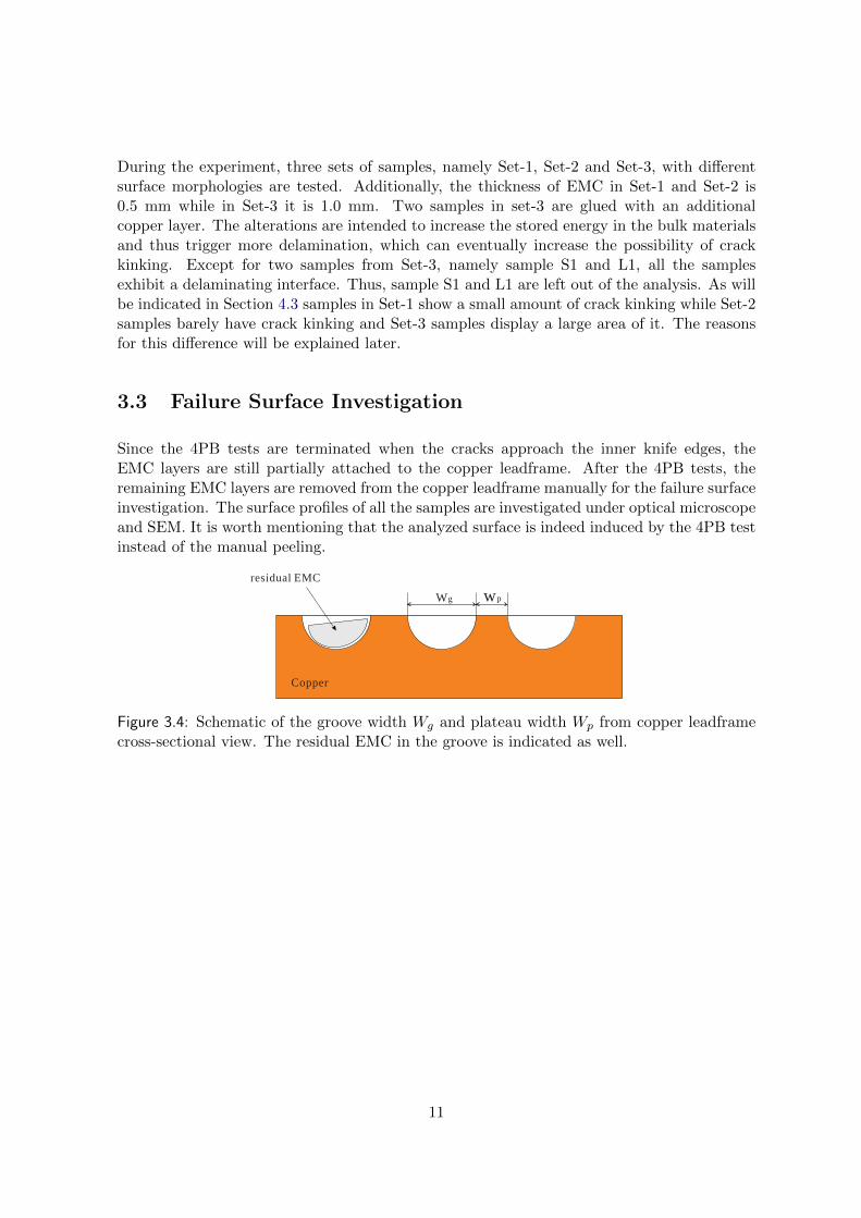
3.3 Failure Surface Investigation
Since the 4PB tests are terminated when the cracks approach the inner knife edges, theEMC layers are still partially attached to the copper leadframe. After the 4PB tests, theremaining EMC layers are removed from the copper leadframe manually for the failure surfaceinvestigation. The surface profiles of all the samples are investigated under optical microscopeand SEM. It is worth mentioning that the analyzed surface is indeed induced by the 4PB testinstead of the manual peeling.
Copper
residual EMC
Wg wp
Figure 3.4: Schematic of the groove width Wg and plateau width Wp from copper leadframecross-sectional view. The residual EMC in the groove is indicated as well.
11

(a) Residual EMC on copper side (b) Algorithm of kinking fractionf computation
Figure 3.5: (a): Some residual EMC on the copper surface highlighted by white ellipse; (b):illustration of the algorithm of computation of kinking fraction.
Firstly, the geometry of the copper surface is analyzed under optical microscope after the4PB test. It consists of the measurement of the groove width Wg and plateau width Wp asshown in Figure 3.4. For both measurements, 15 values from different locations are collectedwhile also the average and standard deviations are computed.
Secondly, the kinking fraction is estimated manually. Due to the etched grooves on the coppersurface, some EMC is left on the copper side (see Figure 3.5). Therefore on the EMC side thestrips are discontinuous, i.e. some portions are left on copper side. The total length Lt of thestrips on the EMC surface is determined. Then the length of the failure parts Lf is counted(represented by red line in Figure 3.5). The kinking fraction f is calculated by f = Lf/Lt.Note that images shown here are from the sample 2 in Set-1, which shows a small amount ofcrack kinking. Samples in Set-2 and Set-3 show different results: Set-2 samples barely havecrack kinking while the grooves of Set-3 samples are fully filled with residual EMC.
Next the data obtained in the previous two steps is assembled and a correlation between thesurface morphology and the kinking fraction f is given.
Finally, the SEM is utilized to examine the failure surface of copper side aiming to have aninsightful investigation of the failure mechanisms.
3.4 Cross-section Investigation
Several cross-section samples are made and investigated with SEM in order to get more detailsof the residual EMC in the etched grooves.
12
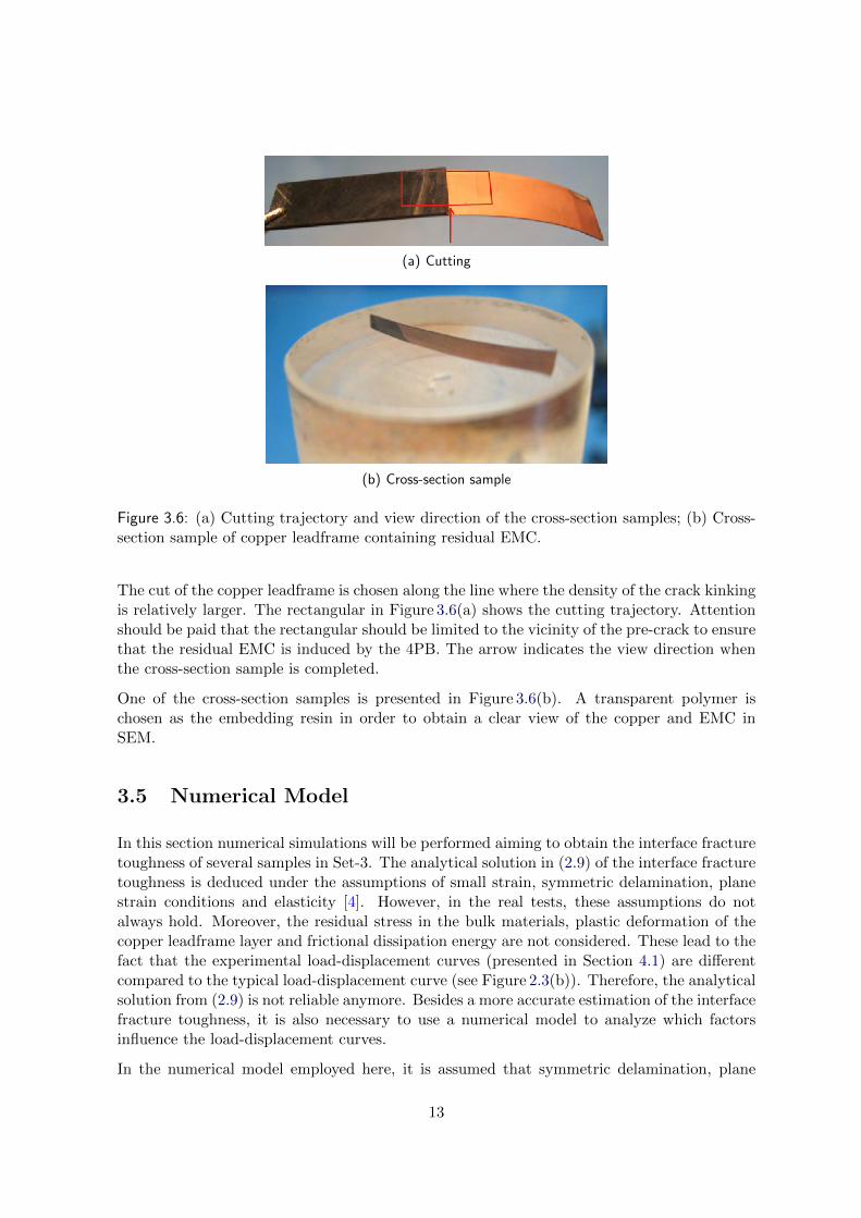
(a) Cutting
(b) Cross-section sample
Figure 3.6: (a) Cutting trajectory and view direction of the cross-section samples; (b) Cross-section sample of copper leadframe containing residual EMC.
The cut of the copper leadframe is chosen along the line where the density of the crack kinkingis relatively larger. The rectangular in Figure 3.6(a) shows the cutting trajectory. Attentionshould be paid that the rectangular should be limited to the vicinity of the pre-crack to ensurethat the residual EMC is induced by the 4PB. The arrow indicates the view direction whenthe cross-section sample is completed.
One of the cross-section samples is presented in Figure 3.6(b). A transparent polymer ischosen as the embedding resin in order to obtain a clear view of the copper and EMC inSEM.
3.5 Numerical Model
In this section numerical simulations will be performed aiming to obtain the interface fracturetoughness of several samples in Set-3. The analytical solution in (2.9) of the interface fracturetoughness is deduced under the assumptions of small strain, symmetric delamination, planestrain conditions and elasticity [4]. However, in the real tests, these assumptions do notalways hold. Moreover, the residual stress in the bulk materials, plastic deformation of thecopper leadframe layer and frictional dissipation energy are not considered. These lead to thefact that the experimental load-displacement curves (presented in Section 4.1) are differentcompared to the typical load-displacement curve (see Figure 2.3(b)). Therefore, the analyticalsolution from (2.9) is not reliable anymore. Besides a more accurate estimation of the interfacefracture toughness, it is also necessary to use a numerical model to analyze which factorsinfluence the load-displacement curves.
In the numerical model employed here, it is assumed that symmetric delamination, plane
13
Support
Symmetry condition
Copper leadframe
EMC
Initial delamination
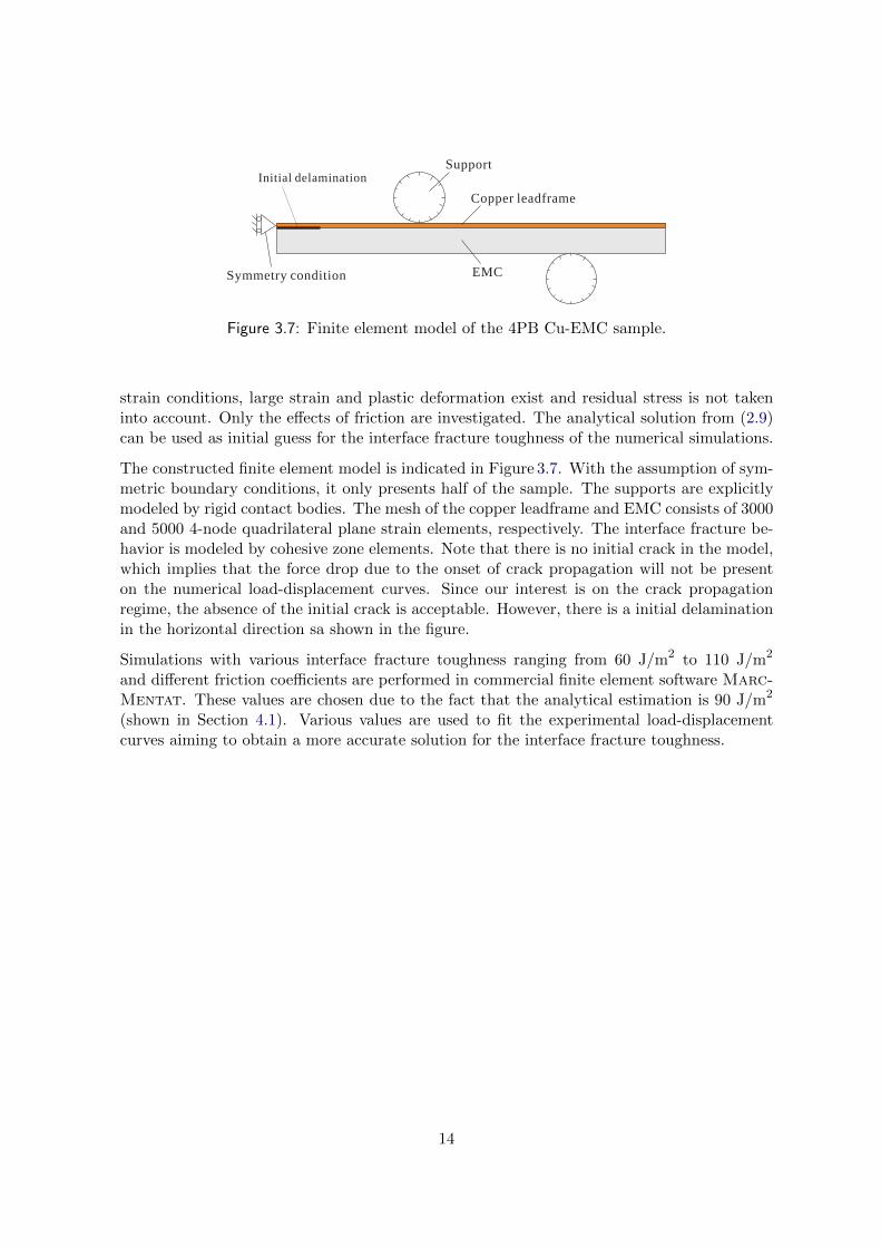
Figure 3.7: Finite element model of the 4PB Cu-EMC sample.
strain conditions, large strain and plastic deformation exist and residual stress is not takeninto account. Only the effects of friction are investigated. The analytical solution from (2.9)can be used as initial guess for the interface fracture toughness of the numerical simulations.
The constructed finite element model is indicated in Figure 3.7. With the assumption of sym-metric boundary conditions, it only presents half of the sample. The supports are explicitlymodeled by rigid contact bodies. The mesh of the copper leadframe and EMC consists of 3000and 5000 4-node quadrilateral plane strain elements, respectively. The interface fracture be-havior is modeled by cohesive zone elements. Note that there is no initial crack in the model,which implies that the force drop due to the onset of crack propagation will not be presenton the numerical load-displacement curves. Since our interest is on the crack propagationregime, the absence of the initial crack is acceptable. However, there is a initial delaminationin the horizontal direction sa shown in the figure.
Simulations with various interface fracture toughness ranging from 60 J/m2 to 110 J/m2
and different friction coefficients are performed in commercial finite element software Marc-Mentat. These values are chosen due to the fact that the analytical estimation is 90 J/m2
(shown in Section 4.1). Various values are used to fit the experimental load-displacementcurves aiming to obtain a more accurate solution for the interface fracture toughness.
14
Chapter 4
Results and Analysis
In this chapter, experimental and numerical results will be presented. Firstly, load-displacementcurves from 4PB tests are illustrated. It is shown that these curves have different shapescompared to the typical load-displacement curve. They can be utilized to extract analyticalsolutions of the interface fracture toughness according to (2.9) as initial guess for the simula-tions. Subsequently, results from numerical simulations with a consideration of nonlinearityare shown aiming to understand the unusual features of the experimental load-displacementcurves. Then the surface morphology of the samples is analyzed in order to relate roughnessprofile to crack kinking fraction f and interface fracture toughness. It turns out that twocategories of crack kinking are observed, namely micro-kinking and intended-kinking and theintended-kinking is more favorable for the profiles with smaller grooves. Finally, SEM imagesof failure surface and cross-section investigation are exhibited and analyzed. They reveal thatbesides the obvious increase of contact area with a factor of approximately 1.5, mechanismslike mechanical interlocking and crack kinking also contribute remarkably to the promotionof the adhesion.
4.1 Load-displacement Curve
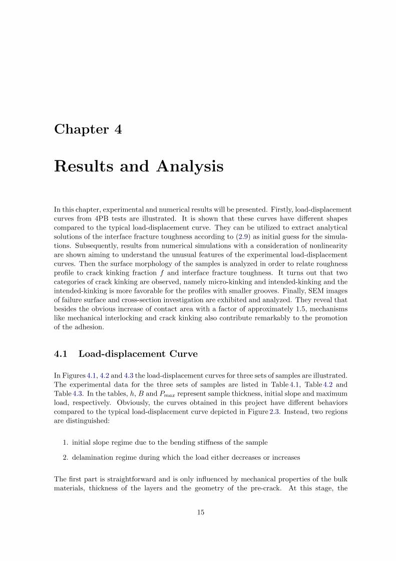
In Figures 4.1, 4.2 and 4.3 the load-displacement curves for three sets of samples are illustrated.The experimental data for the three sets of samples are listed in Table 4.1, Table 4.2 andTable 4.3. In the tables, h, B and Pmax represent sample thickness, initial slope and maximumload, respectively. Obviously, the curves obtained in this project have different behaviorscompared to the typical load-displacement curve depicted in Figure 2.3. Instead, two regionsare distinguished:
1. initial slope regime due to the bending stiffness of the sample
2. delamination regime during which the load either decreases or increases
The first part is straightforward and is only influenced by mechanical properties of the bulkmaterials, thickness of the layers and the geometry of the pre-crack. At this stage, the
15

samples deform elastically accumulating strain energy for subsequent cracking. The typicalstiffness for Set-1 and Set-2 is around 15.00 N/mm. For the Set-3 samples, the thicker EMCand additional glued copper layer lead to higher sample stiffness ranging from 45 N/mm to62 N/mm (see Table 4.3). The second regime, which refers to the crack propagation part,displays a complicated behavior. Instead of forming a steady plateau as the classical solutionexhibits, some curves have an increasing trend at the beginning and decrease after reachingpeaks, the others keep increasing until the end of the test. These unusual features are causedby different nonlinearity factors, which will be further discussed in the next section with theaid of numerical simulations.
Note that at the end of the test, sample C2.1 slips off the set-up, one can see there is asharp drop of the curve in Figure 4.2. Regarding sample W2 and W4 in Figure 4.3, additionalcopper layers of thickness 0.2 mm are glued, which clearly enhances the force levels.
Another apparent nature of all the curves is the serrated shape. Two stages on the curvescan be distinguished (see Figure 4.2). The scale of the serrated shape from the first phase issmaller than the second one. The distance between the peaks in the first phase is typically 50µm, while it is about 125 µm in the second phase. Moreover, the amplitude of the oscillationin the second phase is larger than that of the first phase. It will be indicated later thatthe width of the grooves etched on the copper surface is in the order of 50 µm. Therefore,it is possible that the first phase of the serrated shape is caused by the complicated crackpropagation path induced by the roughened copper surface. Regarding the second phase, itis assumed that the sliding of the samples is responsible for it. In addition, it is found thatthis could also be attributed to unstable operation of the loading motor.
Solution from (2.9) and (2.10) is used as an initial guess for the interface fracture toughnessof the numerical simulations. For all the samples except for W2 and W4, the constant load(Pc) is estimated as 6.5 N. Then the CERR of the sample is around 90 J/m2. Compared tothe CERR of the unetched samples, which is around 10 J/m2, evaluated by M. Kolluri [16],there is a pronounced improvement of the toughness with a factor of nine. Recall that thecontact area increase with a factor of about 1.5, there is additional dissipative mechanisms,which will be demonstrated later.
16
0 1 2 3 4 5 60
1
2
3
4
5
6
7
8
9
Displacement, δ(mm)
Load,P(N
)
Sample 1Sample 2Sample 3Sample 4Sample ASample BSample D
Figure 4.1: Load-displacement curves for sample Set-1.
Table 4.1: Data of Set-1 samples.
Sample h (mm) B (N/mm) Pmax (N)
A 0.7 13.78 6.58
B 0.7 15.22 6.88
D 0.7 15.44 7.33
1 0.7 15.49 7.46
2 0.7 15.39 7.67
3 0.7 14.96 8.42
4 0.7 14.89 7.87
0 1 2 3 4 5 60
1
2
3
4
5
6
7
8
Displacement, δ(mm)
Load,P(N
)
Sample C1.1Sample C1.2Sample C1.3Sample C1.4Sample C2.1Sample C2.2Sample C2.3Sample C2.4
2nd stage1st stage
Figure 4.2: Load-displacement curves for sample Set-2.
Table 4.2: Data for Set-2 samples.
Sample h (mm) B (N/mm) Pmax (N)
C1.1 0.7 16.35 6.95
C1.2 0.7 17.40 7.82
C1.3 0.7 16.74 7.68
C1.4 0.7 17.49 7.30
C2.1 0.7 14.75 6.67
C2.2 0.7 14.79 7.05
C2.3 0.7 17.20 7.45
C2.4 0.7 17.21 6.80
0 0.5 1 1.5 2 2.5 3 3.5 40
5
10
15
20
25
30
35
40
Displacement, δ(mm)
Load,P(N
)
Sample S4Sample L2Sample L3Sample W2Sample W4
Figure 4.3: Load-displacement curves for sample Set-3.
Table 4.3: Data for Set-3 samples.
Sample h (mm) B (N/mm) Pmax (N)
S4 1.2 45.24 7.65
W2 1.4 56.75 37.01
W4 1.4 62.86 34.05
L2 1.2 47.69 8.24
L3 1.2 48.20 7.38
17
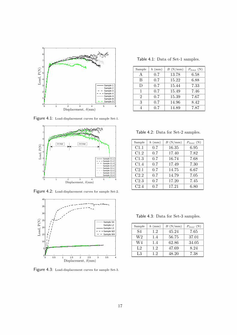
Figure 4.4: Tested samples with permanent deformation.
4.2 Numerical Simulation Results
In order to identify the different phenomena on load-displacement curves mentioned in pre-vious section and obtain a more accurate estimation of the interface fracture toughness, nu-merical simulations are performed. Load-displacement curves from numerical simulations arepresented in Figure 4.5. Results of various interface fracture toughness with friction coefficientη = 0, η = 0.25 and η = 0.50 1 are shown in Figure 4.5(a), Figure 4.5(b) and Figure 4.5(c),respectively. In Figure 4.5(d), interface fracture toughness values and different friction coeffi-cients are indicated. In all figures, an additional horizontal line with Gc = 80 J/m2 and loadP = 6.18 N derived from (2.9) is added to indicate the deviation of the numerical simulationand the analytical solution. It can be observed that as the η value increases, the deviationalso increases. Two phases of the curves can be recognized, namely the initial slope andthe crack propagation regime. The oscillations in the crack propagation regime are possiblyinduced by the element size in the mesh.
Figure 4.5(a) reveals that when friction is not considered, the crack propagation regime dis-plays a plateau. With an increasing interface fracture toughness, the height of the plateauon the load-displacement curves increases. The gray dash line (Gc = 100 J/m2, h = 1.2mm) along with the gray dot line (Gc = 100 J/m2, h = 0.7 mm) show that the thicknessonly alters the initial slope of the curves, the crack propagation regime is not influencedwhen the friction is neglected. However, when the friction coefficient is changed to η = 0.25,Figure 4.5(b) indicates that the thickness of the sample has influence on the crack propaga-tion region. It is further shown that the friction changes the shape of the curves. The lineswith high interface fracture toughness attain an increasing-decreasing shape, which is alsoobserved in the experimental load-displacement curves. As to the Gc = 60 J/m2, it has anincreasing-decreasing-increasing shape, meaning that interface with lower toughness is moresensitive to the friction, which is further confirmed by Figure 4.5(c). Figure 4.5(d) illustrates
1It is the friction between the support and the bulk materials that is considered here.
18
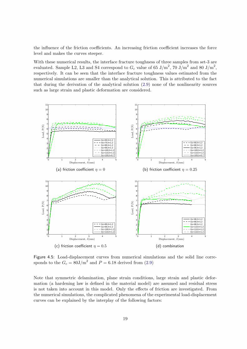
the influence of the friction coefficients. An increasing friction coefficient increases the forcelevel and makes the curves steeper.
With these numerical results, the interface fracture toughness of three samples from set-3 areevaluated. Sample L2, L3 and S4 correspond to Gc value of 65 J/m2, 70 J/m2 and 80 J/m2,respectively. It can be seen that the interface fracture toughness values estimated from thenumerical simulations are smaller than the analytical solution. This is attributed to the factthat during the derivation of the analytical solution (2.9) none of the nonlinearity sourcessuch as large strain and plastic deformation are considered.
0 1 2 3 4 50
1
2
3
4
5
6
7
8
9
10
11
Displacement, δ(mm)
Load,P(N
)
Gc=60,h=1.2Gc=70,h=1.2Gc=80,h=1.2Gc=90,h=1.2Gc=100,h=1.2Gc=110,h=1.2Gc=100,h=0.7
(a) friction coefficient η = 0
0 1 2 3 4 50
1
2
3
4
5
6
7
8
9
10
11
Displacement, δ(mm)
Load,P(N
)
Gc=60,h=1.2Gc=80,h=1.2Gc=90,h=1.2Gc=100,h=1.2Gc=110,h=1.2Gc=100,h=0.7
(b) friction coefficient η = 0.25
0 1 2 3 4 50
1
2
3
4
5
6
7
8
9
10
11
Displacement, δ(mm)
Load,P(N
)
Gc=80,h=1.2Gc=90,h=1.2Gc=100,h=1.2Gc=110,h=1.2
(c) friction coefficient η = 0.5
0 1 2 3 4 50
1
2
3
4
5
6
7
8
9
10
11
Displacement, δ(mm)
Load,P(N
)
Gc=80,h=1.2Gc=80,h=1.2Gc=80,h=1.2Gc=110,h=1.2Gc=110,h=1.2Gc=110,h=1.2
(d) combination
Figure 4.5: Load-displacement curves from numerical simulations and the solid line corre-sponds to the Gc = 80J/m2 and P = 6.18 derived from (2.9)
Note that symmetric delamination, plane strain conditions, large strain and plastic defor-mation (a hardening law is defined in the material model) are assumed and residual stressis not taken into account in this model. Only the effects of friction are investigated. Fromthe numerical simulations, the complicated phenomena of the experimental load-displacementcurves can be explained by the interplay of the following factors:
19
1. Increasing portion of the Mode II fracture during the test. As mentioned earlier, nor-mally the 4PB test consists equal normal and shear displacements on the interface.Nevertheless, this hypothesis does not hold anymore when the crack approaches theinner loading line. The Mode II portion will increase at the vicinity of the inner loadingline, which causes the increase of the mode angle Ψ [4]. Note that the interface frac-ture toughness is not a single material parameter, rather it is a function of the relativeamount of Mode II to Mode I acting on the interface (see Section 2.2). It has beenproven by Wang and Suo [17] that an increasing mode angle Ψ leads to the growth ofthe interface fracture toughness, and thus a load increase. With an increasing Mode IIloading magnitude, the frictional contact between the fracture surfaces and plasticityin adjacent layers also increases, which will also raise the load.
2. Plastic deformation. It can be seen from Figure 3.3 and Figure 4.4 that the samplesshow permanent deformation after the test. It indicates that the work of separation isnot only used for the crack propagation, but also for the plastic bending of the sample.However, numerical simulation reveals plastic deformation will actually decrease theload [18]. This observation requires additional verification.
3. Sliding behavior of the samples from the knife edges. As the experiment goes on, thedeformation of the samples becomes large, which makes the samples slide from the knifeedges. From (2.9), with a certain interface fracture toughness Gc, the sliding behaviorof the samples will decrease the effective loading span L, thus increase the load neededfor a certain crack propagation.
4. Frictional contact. Numerical simulations show that the consideration of frictional dis-sipation energy will increase the force levels.
5. Residual stress and symmetry. Although these factors are not considered here, thesemight affect the load-displacement curves.
4.3 Surface Morphology
The surface morphology investigation is carried out to relate the surface profiles to crackkinking and interface fracture toughness. The results for the surface investigation are listedin Table 4.4, Table 4.5 and Table 4.6. Since sample A and sample B in Set-1 are not etchedproperly as shown in Figure 4.7, they are removed from the analysis. Furthermore, the errorbar plot for this data is presented in Figure 4.6.
Table 4.4: Surface profile of sample Set-1.
Sample ID Wg (µm) Wp (µm) Kinking fraction [%] Wg/Wp ratio
1 31.30±1.48 58.64±0.67 12.86 0.53
2 33.49±1.15 57.37±1.66 14.82 0.58
3 37.49±0.65 51.58±0.76 3.88 0.73
4 35.12±1.67 53.96±1.41 5.41 0.68
C 22.15±0.99 55.98±1.06 1.31 0.39
D 20.80±0.76 58.08±0.82 2.80 0.35
20
Table 4.5: Surface profiles of sample Set-2.
Sample ID Wg (µm) Wp (µm) Kinking fraction [%] Wg/Wp ratio
C1.1 56.61±0.94 33.16±1.39 0 1.70
C1.2 56.90±0.62 32.75±0.62 0 1.70
C1.3 61.48±1.20 28.88±1.37 0 2.10
C1.4 60.23±1.21 29.24±0.61 0 2.07
C2.1 55.96±0.72 24.50±1.33 0 2.30
C2.2 55.22±0.86 25.46±1.18 0 2.20
C2.3 62.59±0.95 18.26±0.88 2.54 3.50
C2.4 61.33±0.90 19.07±1.09 1.24 3.21
Table 4.6: Surface profile of sample Set-3.
Sample suffix Wg (µm) Wp (µm) Kinking fraction Wg/Wp ratio
1 31.29±1.29 60.15±1.21 full 0.52
2 37.12±0.75 53.08±1.75 full 0.70
3 38.18±1.65 44.69±0.58 full 0.85
4 46.53±1.96 33.72±1.79 full 1.37
0 1 2 3 4 5 6 720
25
30
35
40
45
50
55
60
Sample ID
Width
[µm]
Groove widthPlateau width
(a) Error bar plot for sample Set-1
0 1 2 3 4 5 6 7 8 915
20
25
30
35
40
45
50
55
60
65
Sample ID
Width
[µm]
Groove widthPlateau width
(b) Error bar plot for sample Set-2
Figure 4.6: Error bar plot for surface profiles of two sets of samples.
From the tables and figures given above, it can be seen that the crucial difference of sampleSet-1 and sample Set-2 is the values of the Groove/Plateau ratio. In Set-1 the width of theplateau WP is 2-3 times as large as that of the groove WG and in Set-2 it is vice versa.From the kinking fraction of Table 4.4 and Table 4.5, it can be concluded that kinking is morefavorable for the profiles with smaller grooves. Kim et al reported an opposite results [10].Note that the relatively higher value of kinking fraction for sample 1 and sample 2 is due tothe occurrence of the edge effect (more kinking at the edge, see Figure 4.8). As to the sampleSet-3, the thickness of EMC is increased from 0.5 mm to 1.0 mm. Apparently, the thickerEMC helps to form more kinking.
21

The key conclusion is that the simplified 2D profiles are able to trigger crack kinking. Dueto the limited variations, which combination of groove width and plateau width is optimalfor crack kinking still remains an unknown. Another interesting thing is that Set-2 samplesbarely have crack kinking while the grooves of Set-3 samples are fully filled with residual EMC.However, such a significant difference is not observed for the interface fracture toughnessvalues according to the load-displacement curves in Figure 4.2 and Figure 4.3. It is expectedthat crack kinking is not the only mechanism that contributes to the enhancement of theadhesion. It is necessary to analyze the failure surface and cross-section of Set-2 and Set-3samples in SEM to obtain more details.
(a) Sample A (b) Sample B
Figure 4.7: Optical microscope images of failure surface at copper side for sample A (a) andsample B (b) .
(a) Sample 1 (b) Sample 2
Figure 4.8: Edge effect of sample 1 and sample 2.
22

4.4 Failure Surface SEM Images
In Figure 4.9 four SEM images of the copper leadframe failure surface from sample Set-2 andSet-3 are shown. Figure 4.9(a) and Figure 4.9(b) are back scattered electron detector (BSED)image and Everhart-Thornley detector (ETD) image, respectively, and both from the Set-2sample C2.3. These images illustrate the typical topography of the failure surface, exhibitingresidual EMC on the copper side.
In the BSED image, two major colors, namely black and white, can be distinguished. Theblack portion represents residual EMC, while the white counterpart stands for exposed coppersurface. For the residual EMC, it can be further divided into two categories: micro-kinkingand intended-kinking. The micro-kinking has a discontinuous feature, stochastically spreadingover the copper surface, both in the groove and on the plateau. The intended-kinking blocks,which have a relatively larger dimension compared to the micro-kinking, are only located inthe grooves. Note that micro-kinking is believed to be induced by the small scale roughnessand the physical interactions between bulk materials. These imply that the secondary bondsacross the interface are strong enough to cause crack deflection into the epoxy resin, resultingin a partial cohesive failure mode. The intended-kinking is the cohesive failure mode whichis present when a well-defined roughness pattern is applied on the copper surface.
For the ETD image, it is worth mentioning that there are only micro-kinking in the imageand the white spots in the field are induced by the electron charging. A clear differencebetween the topography in the groove and on the plateau can be recognized. The densityof the micro-kinking in the groove is much larger than that on the plateau. Almost 95% ofarea in the groove is covered by the residual EMC. The reason for this is a consequence ofthe different asperity at these two areas. Since the grooves are produced by etching, theyare much rougher than the surface on the plateau (see Figure 4.10). It is not surprising thatmore micro-kinking in the grooves is present. The higher number of EMC remnants in thegrooves also indicate the frictional resistance during the pull out of the interlocked EMC.Note that Figure 4.9(b) is a representative image of the Set-2 sample failure surface, showingmicro-kinking in the whole view. However, Figure 4.9(a) displays a typical location whereintended-kinking and micro-kinking both exist.
Figures 4.9(c) and Figure 4.9(d) indicate the failure surface of sample S4 from Set-3. It can beseen that the grooves on the copper substrate are almost fully filled with the residual EMC,showing that numerous intended-kinking occurred during the 4PB test for this sample. Theright part of the Figure 4.9(c) is the place where the pre-crack is located. This part is includedin order to indicate that the image is taken in the vicinity of pre-crack, implying that thefailure surface in the view is induced by the 4PB test instead of the peeling after the test.Figure 4.9(d) also displays a small portion of adhesive failure. In the groove, micro-kinkingcan be found as well.
Recall that the contact area increases with a factor of about 1.5 and the interface fracturetoughness increases with a factor of nine. Now it can be concluded that the crack kinking isa main contributor to the dissipative energy. The observed micro-kinking partially explainssimilar load-displacement curves of Set-2 and Set-3 samples. The micro-kinking, one type ofcohesive failure mechanisms, caused by the molecular decohesion of the EMC, also consumeslarge amount of energy for crack propagation. It should be emphasized that the dense micro-
23
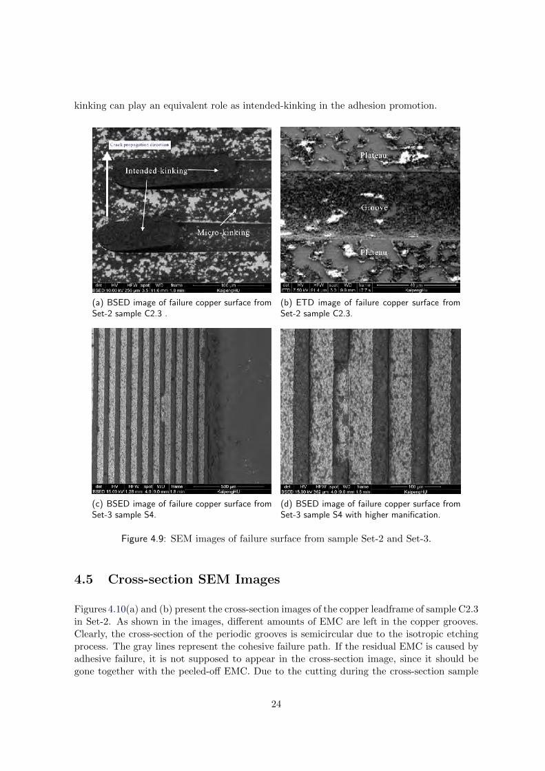
kinking can play an equivalent role as intended-kinking in the adhesion promotion.
(a) BSED image of failure copper surface fromSet-2 sample C2.3 .
(b) ETD image of failure copper surface fromSet-2 sample C2.3.
(c) BSED image of failure copper surface fromSet-3 sample S4.
(d) BSED image of failure copper surface fromSet-3 sample S4 with higher manification.
Figure 4.9: SEM images of failure surface from sample Set-2 and Set-3.
4.5 Cross-section SEM Images
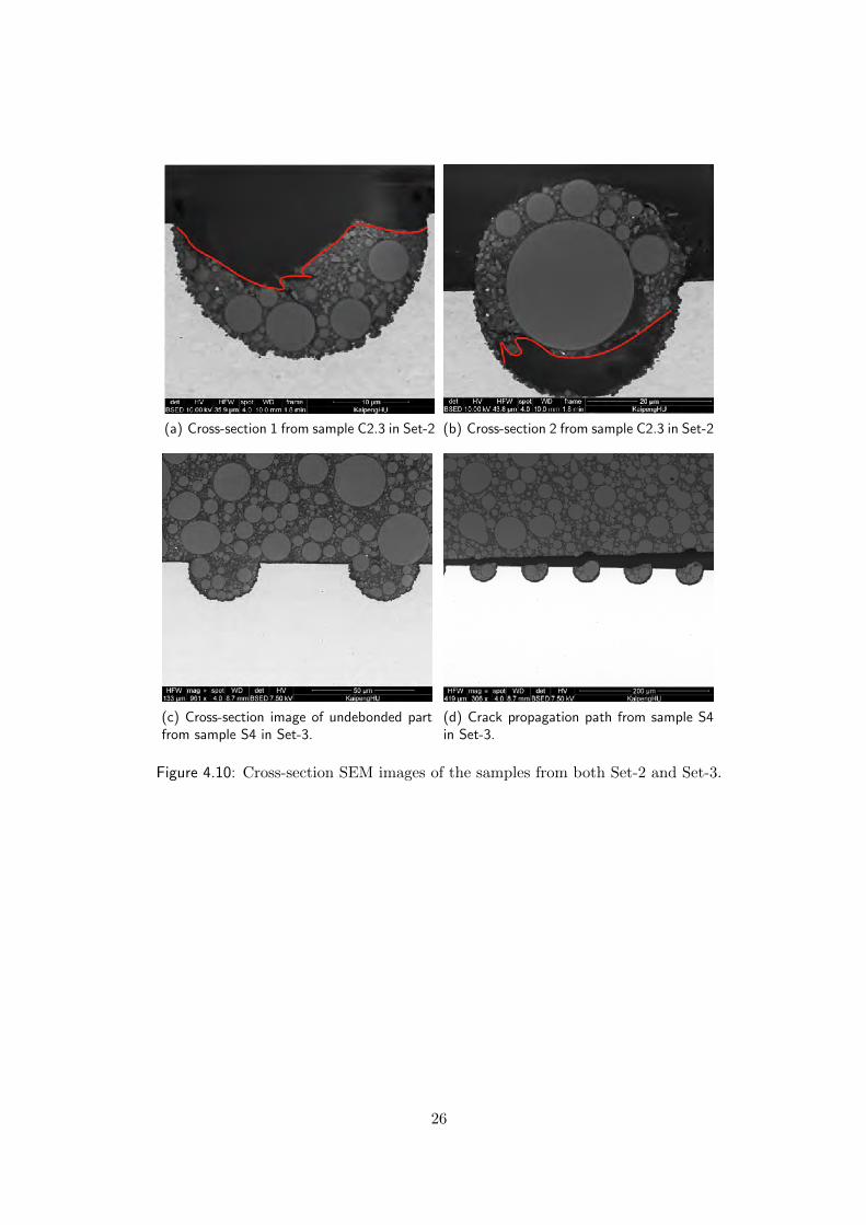
Figures 4.10(a) and (b) present the cross-section images of the copper leadframe of sample C2.3in Set-2. As shown in the images, different amounts of EMC are left in the copper grooves.Clearly, the cross-section of the periodic grooves is semicircular due to the isotropic etchingprocess. The gray lines represent the cohesive failure path. If the residual EMC is caused byadhesive failure, it is not supposed to appear in the cross-section image, since it should begone together with the peeled-off EMC. Due to the cutting during the cross-section sample
24
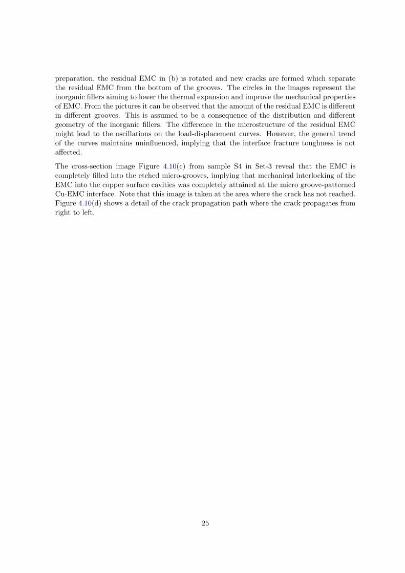
preparation, the residual EMC in (b) is rotated and new cracks are formed which separatethe residual EMC from the bottom of the grooves. The circles in the images represent theinorganic fillers aiming to lower the thermal expansion and improve the mechanical propertiesof EMC. From the pictures it can be observed that the amount of the residual EMC is differentin different grooves. This is assumed to be a consequence of the distribution and differentgeometry of the inorganic fillers. The difference in the microstructure of the residual EMCmight lead to the oscillations on the load-displacement curves. However, the general trendof the curves maintains uninfluenced, implying that the interface fracture toughness is notaffected.
The cross-section image Figure 4.10(c) from sample S4 in Set-3 reveal that the EMC iscompletely filled into the etched micro-grooves, implying that mechanical interlocking of theEMC into the copper surface cavities was completely attained at the micro groove-patternedCu-EMC interface. Note that this image is taken at the area where the crack has not reached.Figure 4.10(d) shows a detail of the crack propagation path where the crack propagates fromright to left.
25
(a) Cross-section 1 from sample C2.3 in Set-2 (b) Cross-section 2 from sample C2.3 in Set-2
(c) Cross-section image of undebonded partfrom sample S4 in Set-3.
(d) Crack propagation path from sample S4in Set-3.
Figure 4.10: Cross-section SEM images of the samples from both Set-2 and Set-3.
26

Chapter 5
Conclusions and Recommendations
5.1 Conclusions
In this work, the interface fracture toughness of Cu-EMC bimaterial strip with well-definedmicroscopic roughness pattern on copper surface is investigated experimentally and numeri-cally. 4PB test is adopted in the experiment. The main conclusions are summarized below:
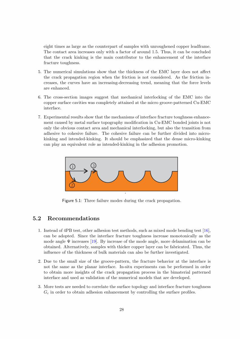
1. Three basic failure modes for 4PB experiment during the crack propagation process areobserved (see Figure 5.1). The first one is pure cohesive failure mode, which is calledintended-cracking in the preceding chapters. The second one and the third one are thecombinations of cohesive failure (only micro-kinking) and adhesive failure (clear delam-ination of bulk materials). However, the second one presents at the groove surface whilethe third one occurs at the plateau surface. The results of failure surface SEM inves-tigation presents a clear topology difference between the etched grooves and plateau.The density of micro-kinking in the grooves is much larger due to the rougher groovesurface derived from the chemical etching.
2. The simplified 2D profiles are able to trigger reproducible crack kinking. Due to thelimited variations, which combination of groove width and plateau width is optimalfor more crack kinking still remains an unknown. However, the evaluation of kinkingfraction f shows that the profile of the copper leadframe surface has an influence on thekinking fraction f . The intended-kinking is more favorable when the groove width Wg
is smaller than the plateau width Wp.
3. The load-displacement curves from 4PB show that the interface does not debond in asteady manner. With the interplay of friction dissipation, plastic deformation, slidingbehavior, increasing portion of the Mode II fracture and residual stress, the curvesdisplay an obvious discrepancy from the typical load-displacement curve.
4. The interface fracture toughness of the Cu-EMC sample is measured to be around 90J/m2, determined from analytical method. With the aid of simulations, the value isfinally determined between 65 J/m2 and 80 J/m2. The difference indicates that theanalytical solution is an overestimation of the interface fracture toughness. It is six to
27
eight times as large as the counterpart of samples with unroughened copper leadframe.The contact area increases only with a factor of around 1.5. Thus, it can be concludedthat the crack kinking is the main contributor to the enhancement of the interfacefracture toughness.
5. The numerical simulations show that the thickness of the EMC layer does not affectthe crack propagation region when the friction is not considered. As the friction in-creases, the curves have an increasing-decreasing trend, meaning that the force levelsare enhanced.
6. The cross-section images suggest that mechanical interlocking of the EMC into thecopper surface cavities was completely attained at the micro groove-patterned Cu-EMCinterface.
7. Experimental results show that the mechanisms of interface fracture toughness enhance-ment caused by metal surface topography modification in Cu-EMC bonded joints is notonly the obvious contact area and mechanical interlocking, but also the transition fromadhesive to cohesive failure. The cohesive failure can be further divided into micro-kinking and intended-kinking. It should be emphasized that the dense micro-kinkingcan play an equivalent role as intended-kinking in the adhesion promotion.
1
2
3
Figure 5.1: Three failure modes during the crack propagation.
5.2 Recommendations
1. Instead of 4PB test, other adhesion test methods, such as mixed mode bending test [16],can be adopted. Since the interface fracture toughness increase monotonically as themode angle Ψ increases [19]. By increase of the mode angle, more delamination can beobtained. Alternatively, samples with thicker copper layer can be fabricated. Thus, theinfluence of the thickness of bulk materials can also be further investigated.
2. Due to the small size of the groove-pattern, the fracture behavior at the interface isnot the same as the planar interface. In-situ experiments can be performed in orderto obtain more insights of the crack propagation process in the bimaterial patternedinterface and used as validation of the numerical models that are developed.
3. More tests are needed to correlate the surface topology and interface fracture toughnessGc in order to obtain adhesion enhancement by controlling the surface profiles.
28
Bibliography
[1] G. Q. Zhang, W. D. Van Driel, and X. J. Fan. Mechanics of Microelectronics. Springer,Dordrecht, 2006.
[2] Ming-Yuan. He and J. W. Hutchinson. Crack deflection at an interface between dissimilarelastic materials. International Journal of Solids and Structures, 25(9):1053–1067, 1989.
[3] R. H. Dauskardt, M. Lane, Q. Ma, and N. Krishna. Adhesion and debonding of multi-layer thin film structures. Engineering Fracture Mechanics, 61(1):141–162, 1998.
[4] P. G. Charalambides, J. Lund, A. G. Evans, and R. M. McMeeking. Test specimen for de-termining the fracture resistance of bimaterial interfaces. Journal of Applied Mechanics,Transactions ASME, 56(1):77–82, 1989.
[5] Z. Gan, S. G. Mhaisalkar, Z. Chen, S. Zhang, Z. Chen, and K. Prasad. Study of interfacialadhesion energy of multilayered ulsi thin film structures using four-point bending test.Surface and Coatings Technology, 198(1-3 SPEC. ISS.):85–89, 2005.
[6] E. D. Reedy. Effects of patterned nanoscale interfacial roughness on interfacial toughness:A finite element analysis. Journal of Materials Research, 23(11):3056–3065, 2008.
[7] S. P. M. Noijen, O. van der Sluis, P. H. M. Timmermans, and G. Q. Zhang. Numericalprediction of failure paths at a roughened metal/polymer interface. MicroelectronicsReliability, 49(9-11):1315–1318, 2009.
[8] Q. Yao and J. Qu. Interfacial versus cohesive failure on polymer-metal interfaces inelectronic packaging - effects of interface roughness. Journal of Electronic Packaging,Transactions of the ASME, 124(2):127–134, 2002.
[9] Kenneth M. Liechti. Fracture mechanics and singularities in bonded systems. In D. A.Dillard and A. V. Pocius, editors, The mechanics of adhesion, chapter 2, pages 45–75.Elsevier Science B.V., Amsterdam, 2002.
[10] W. S. Kim, I. H. Yun, J. J. Lee, and H. T. Jung. Evaluation of mechanical interlockeffect on adhesion strength of polymermetal interfaces using micro-patterned surfacetopography. International Journal of Adhesion and Adhesives, 30(6):408–417, 2010.
[11] H. Y. Lee and J. Qu. Microstructure, adhesion strength and failure path at a poly-mer/roughened metal interface. Journal of Adhesion Science and Technology, 17(2):195–215, 2003.
29
[12] C. K. Y. Wong, H. Fan, and M. M. F. Yuen. Investigation of adhesion properties of cu-emc interface by molecular dynamic simulation. In Proceedings of the 6th InternationalConference on Thermal, Mechanical and Multi-Physics Simulation and Experiments inMicro-Electronics and Micro-Systems - EuroSimE 2005, pages 31–35, 2005.
[13] A. Xiao, H. Pape, G. Schlottig, Wunderle, Y. Y. Leung, K. M. B. Jansen, and L. J.Ernst. Procedure to determine interfacial toughness of emc-copper (oxide) interfaces. InProceedings - 2010 11th International Conference on Electronic Packaging Technologyand High Density Packaging, ICEPT-HDP 2010, pages 356–362, 2010.
[14] O. Van Der Sluis, S. P. M. Noijen, J. B. Bouquet, and P. H. M. Timmermans. Analysis ofcombined adhesive and cohesive cracking at roughened surfaces, volume 488-489 of KeyEngineering Materials. 2012.
[15] J. Dundurs. Edge-bonded dissimilar orthogonal elastic wedges. Journal of Applied Me-chanics, 36:650–652, 1969.
[16] M. Kolluri, J. P. M. Hoefnagels, J. A. W. Van Dommelen, and M. G. D. Geers. Animproved miniature mixed-mode delamination setup for in situ microscopic interfacefailure analyses. Journal of Physics D: Applied Physics, 44(3), 2011.
[17] J. S. Wang and Z. Suo. Experimental determination of interfacial toughness curves usingbrazil-nut-sandwiches. Acta Metallurgica Et Materialia, 38(7):1279–1290, 1990.
[18] S. P. M. Noijen. 4pb test of structured l/f-emc interface. Technical report, PhilipsResearch, Eindhoven, 2011.
[19] J. W. Hutchinson. Mixed mode cracking in layered materials. Advances in AppliedMechanics, 29:63–191, 1992.
30

Acknowledgements
I would like to express my gratitude to all those who helped to complete this internshipreport. First, I want to offer my sincerest gratitude to one of my supervisors, Olaf van derSluis, for offering me the chance to do the internship in Phillips Research in Eindhoven.I am grateful for his useful guidance, valuable encouragement and consistent patience. Iwould like to thank Sander Noijen for offering me a lot of help in numerical parts. Manythanks to Peter Timmermans from Philips Research, for supporting me in arrangement ofthe experiments and helpful discussion during the weekly meetings. Furthermore, I would liketo thank Ron Hovenkamp for his help during the experiments in the Mechanical Test Lab inPhilips Research. Finally, I would like to thank Marc van Maris for his experimental guidanceabout how to operate the advanced equipments in the Multi Scale Lab of the TechnicalUniversity of Eindhoven.
31
