in a 2128
TRANSCRIPT

8/6/2019 In a 2128
http://slidepdf.com/reader/full/in-a-2128 1/12
©1994 Burr-Brown Corporation PDS-1243C Printed in U.S.A. January, 1996
FEATURESq LOW OFFSET VOLTAGE: 50 µV maxq LOW DRIFT: 0.5 µV/°C maxq LOW INPUT BIAS CURRENT: 5nA maxq HIGH CMR: 120dB minq INPUTS PROTECTED TO ±40Vq WIDE SUPPLY RANGE: ±2.25V to ±18Vq LOW QUIESCENT CURRENT: 700 µA / IAq 16-PIN PLASTIC DIP, SOL-16
DESCRIPTIONThe INA2128 is a dual, low power, general purposeinstrumentation amplifier offering excellent accuracy.Its versatile 3-op amp design and small size make itideal for a wide range of applications. Current-feedback input circuitry provides wide bandwidth even at highgain (200kHz at G = 100).
A single external resistor sets any gain from 1 to 10,000.Internal input protection can withstand up to ±40Vwithout damage.
The INA2128 is laser trimmed for very low offsetvoltage (50 µV), drift (0.5 µV/ °C) and high common-mode rejection (120dB at G ≥ 100). It operates withpower supplies as low as ±2.25V, and quiescent currentis only 700 µA per IA—ideal for battery operated andmultiple-channel systems.
The INA2128 is available in 16-pin plastic DIP, andSOL-16 surface-mount packages, specified for the–40 °C to +85 °C temperature range.
APPLICATIONSq SENSOR AMPLIFIER
THERMOCOUPLE, RTD, BRIDGEq MEDICAL INSTRUMENTATIONq MULTIPLE-CHANNEL SYSTEMS
q BATTERY OPERATED EQUIPMENT
Dual, Low PowerINSTRUMENTATION AMPLIFIER
INA2128
A 1A
A 2A
A 3A
40k Ω40k Ω
40k Ω40k Ω
VINA1
3
4
2
16
14
13
15
7
6
5
10
11
12
VINA
RGA
V+
V–
INA2128
Ref A
VOA
GA = 1 + 50k Ω
RGA
–
+
Over-VoltageProtection
25k Ω
25k Ω
Over-VoltageProtection
A 1B
A 2B
A 3B
40k Ω40k Ω
8
9
40k Ω40k Ω
VINB
VINB
RGB
Ref B
VOB
GB = 1 + 50k ΩRGB
–
+
Over-VoltageProtection
25k Ω
25k Ω
Over-VoltageProtection
®
International Airport Industrial Park • Mailing Address: PO Box 11400, Tucson, AZ 85734 • Street Address: 6730 S. Tucson Blvd., Tucson, AZ 85706 • Tel: (520) 746-1111 • Twx: 910-952-11Internet: http://www.burr-brown.com/ • FAXL ine: (800) 548-6133 (US/Canada Only) • Cable: BBRCORP • Telex: 066-6491 • FAX: (520) 889-1510 • Im mediate Product Info: (800) 548-61
I N A 2 1 2 8
I N A 2 1 2 8
SBOS035

8/6/2019 In a 2128
http://slidepdf.com/reader/full/in-a-2128 2/12
®
INA2128 2
SPECIFICATIONSAt TA = +25 °C, V S = ±15V, R L = 10k Ω, unless otherwise noted.
INA2128P, U INA2128PA, UA
PARAMETER CONDITIONS MIN TYP MAX MIN TYP MAX UNITS
INPUTOffset Voltage, RTI
Initial TA = +25 °C ±10 ±100/G ±50 ±500/G ±25 ±100/G ±125 ±1000/G µVvs Temperature T A = TMIN to T MAX ±0.2 ± 2/G ±0.5 ± 20/G ±0.2 ± 5/G ±1 ± 20/G µV/ °C
vs Power Supply V S = ±2.25V to ±18V ±0.2 ±20/G ±1 ±100/GT
±2 ±200/G µV/VLong-Term Stability ±0.1 ±3/G T µV/moImpedance, Differential 10 10 || 2 T Ω || pF
Common-Mode 10 11 || 9 T Ω || pFCommon-Mode Voltage Range (1) VO = 0V (V+) – 2 (V+) – 1.4 T T V
(V–) + 2 (V–) + 1.7 T T VSafe Input Voltage ±40 T VCommon-Mode Rejection V CM = ±13V, ∆RS = 1k Ω
G=1 80 86 73 T dBG=10 100 106 93 T dBG=100 120 125 110 T dB
G=1000 120 130 110 T dB
BIAS CURRENT ±2 ±5 T ±10 nAvs Temperature ±30 T pA/ °C
Offset Current ±1 ±5 T ±10 nAvs Temperature ±30 T pA/ °C
NOISE VOLTAGE, RTI G = 1000, R S = 0 Ωf = 10Hz 10 T nV/ √Hzf = 100Hz 8 T nV/ √Hzf = 1kHz 8 T nV/ √HzfB = 0.1Hz to 10Hz 0.2 T µVp-p
Noise Currentf=10Hz 0.9 T pA/ √Hzf=1kHz 0.3 T pA/ √HzfB = 0.1Hz to 10Hz 30 T pAp-p
GAINGain Equation 1 + (50k Ω /RG) T V/VRange of Gain 1 10000 T T V/VGain Error G=1 ±0.01 ±0.024 T ±0.1 %
G=10 ±0.02 ±0.4 T ±0.5 %G=100 ±0.05 ±0.5 T ±0.7 %
G=1000 ±0.5 ±1 T ±2 %Gain vs Temperature (2) G=1 ±1 ±10 T T ppm/ °C
50kΩ Resistance (2, 3) ±25 ±100 T T ppm/ °CNonlinearity V O = ±13.6V, G=1 ±0.0001 ±0.001 T ±0.002 % of FSR
G=10 ±0.0003 ±0.002 T ±0.004 % of FSRG=100 ±0.0005 ±0.002 T ±0.004 % of FSR
G=1000 ±0.001 (Note 4) T T % of FSR
OUTPUTVoltage: Positive R L = 10k Ω (V+) – 1.4 (V+) – 0.9 T T V
Negative R L = 10k Ω (V–) + 1.4 (V–) + 0.8 T T VLoad Capacitance Stability 1000 T pFShort-Circuit Current +6/–15 T mA
FREQUENCY RESPONSEBandwidth, –3dB G=1 1.3 T MHz
G=10 700 T kHzG=100 200 T kHz
G=1000 20 T kHzSlew Rate V O = ±10V, G=10 4 T V/ µsSettling Time, 0.01% G=1 7 T µs
G=10 7 T µsG=100 9 T µs
G=1000 80 T µsOverload Recovery 50% Overdrive 4 T µs
POWER SUPPLYVoltage Range ±2.25 ±15 ±18 T T T VCurrent, Total V IN = 0V ±1.4 ±1.5 T T mA
TEMPERATURE RANGESpecification –40 85 T T °COperating –40 125 T T °Cθ JA 80 T °C/W
T Specification same as INA2128P, U.
NOTE: (1) Input common-mode range varies with output voltage—see typical curves. (2) Guaranteed by wafer test. (3) Temperature coefficient of the “50k Ω” term inthe gain equation. (4) Nonlinearity measurements in G = 1000 are dominated by noise. Typical nonlinearity is ±0.001%.
The information provided herein is believed to be reliable; however, BURR-BROWN assumes no responsibility for inaccuracies or omissions. BURR-BROWN assumesno responsibility for the use of this information, and all use of such information shall be entirely at the user’s own risk. Prices and specifications are subject to changewithout notice. No patent rights or licenses to any of the circuits described herein are implied or granted to any third party. BURR-BROWN does not authorize or warrantany BURR-BROWN product for use in life support devices and/or systems.
8/6/2019 In a 2128
http://slidepdf.com/reader/full/in-a-2128 3/12
®
INA21283
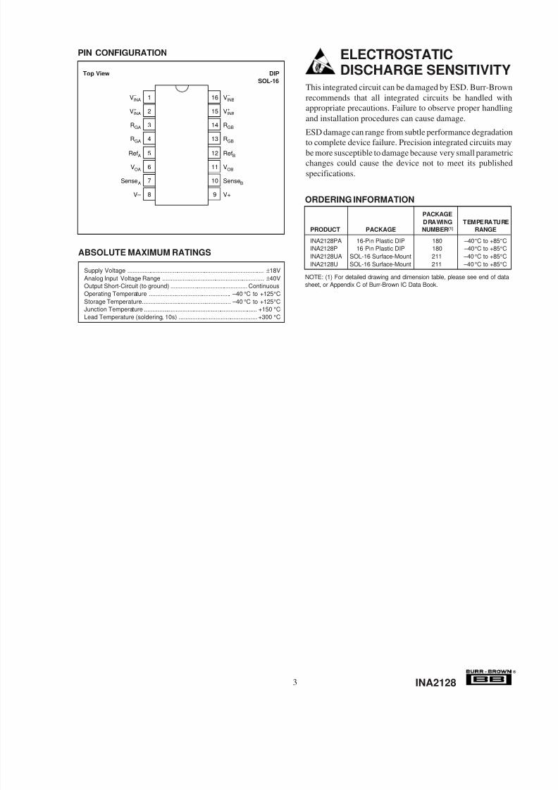
Supply Voltage .................................................................................. ±18VAnalog Input Voltage Range ............................................................. ±40VOutput Short-Circuit (to ground) .............................................. ContinuousOperating Temperature ................................................. –40 °C to +125 °CStorage Temperature..................................................... –40 °C to +125 °CJunction Temperature .................................................................... +150 °CLead Temperature (soldering, 10s) ............................................... +300 °C
ABSOLUTE MAXIMUM RATINGS
PIN CONFIGURATION
Top View DIPSOL-16
VINA
VINA
RGA
RGA
VINB
VINB
RGB
RGB
1
2
3
4
Ref A
VOA
Sense A
V–
5
6
7
8
16
15
14
13
Ref B
VOB
Sense B
V+
12
11
10
9
–
+
–
+
ELECTROSTATICDISCHARGE SENSITIVITY
This integrated circuit can be damaged by ESD. Burr-Brownrecommends that all integrated circuits be handled withappropriate precautions. Failure to observe proper handlingand installation procedures can cause damage.
ESD damage can range from subtle performance degradationto complete device failure. Precision integrated circuits maybe more susceptible to damage because very small parametricchanges could cause the device not to meet its publishedspecifications.
ORDERING INFORMATION
PACKAGEDRAWING TEMPERATURE
PRODUCT PACKAGE NUMBER (1) RANGE
INA2128PA 16-Pin Plastic DIP 180 –40 °C to +85 °CINA2128P 16-Pin Plastic DIP 180 –40 °C to +85 °CINA2128UA SOL-16 Surface-Mount 211 –40 °C to +85 °CINA2128U SOL-16 Surface-Mount 211 –40 °C to +85 °C
NOTE: (1) For detailed drawing and dimension table, please see end of datasheet, or Appendix C of Burr-Brown IC Data Book.
8/6/2019 In a 2128
http://slidepdf.com/reader/full/in-a-2128 4/12
®
INA2128 4
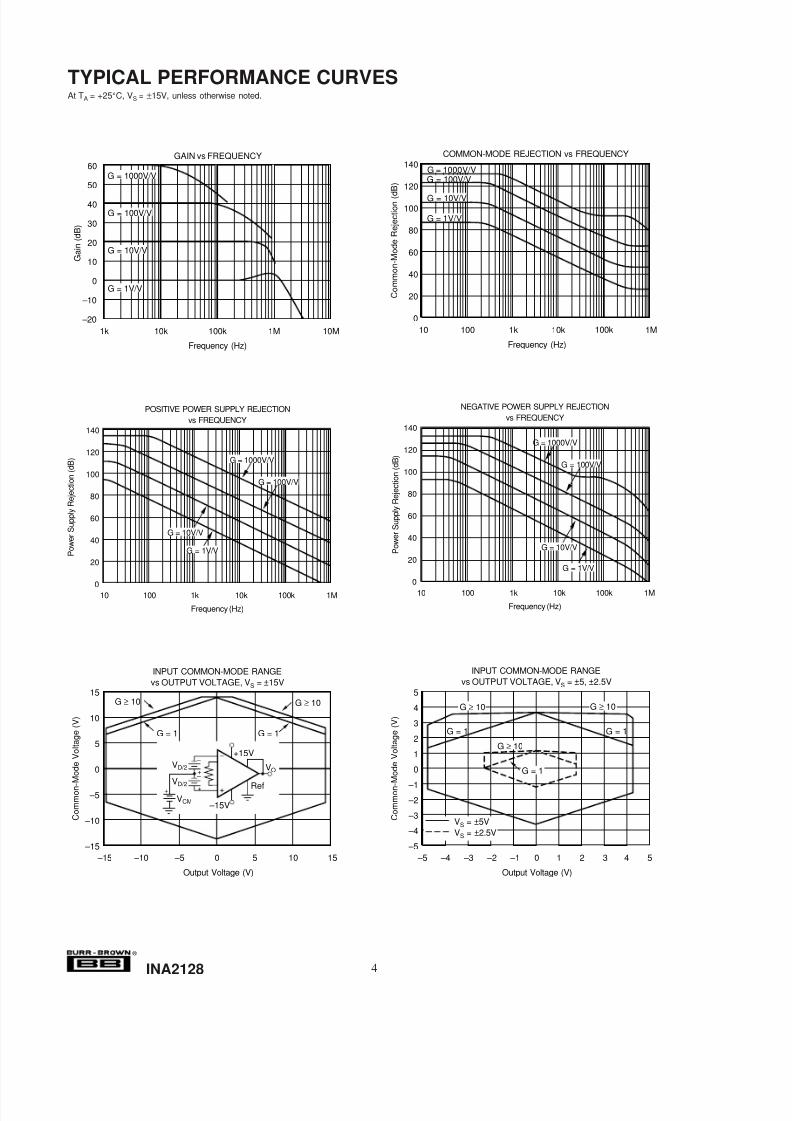
INPUT COMMON-MODE RANGEvs OUTPUT VOLTAGE, V S = ±5, ±2.5V
Output Voltage (V)
C o m m o n -
M o d e
V o l t a g e
( V )
–5
5
4
3
2
1
0
–1 –2
–3
–4
–5 –4 –3 –2 –1 0 1 2 3 4 5
VS = ±5VVS = ±2.5V
G = 1 G = 1
G ≥ 10 G ≥ 10
G ≥ 10
G = 1
INPUT COMMON-MODE RANGEvs OUTPUT VOLTAGE, V S = ±15V
Output Voltage (V)
C o m m o n -
M o d e
V o
l t a g e
( V )
–15 –10 0 5 15 –5
15
10
5
0
–5
–10
–1510
G = 1 G = 1
G ≥ 10 G ≥ 10
VD/2 –
+ –
+
VCM
VO
VD/2 Ref
–15V
+15V
+
TYPICAL PERFORMANCE CURVESAt TA = +25 °C, V S = ±15V, unless otherwise noted.
POSITIVE POWER SUPPLY REJECTIONvs FREQUENCY
Frequency (Hz)
P o w e r
S u p p l y
R e j e c t i o n
( d B )
140
120
100
80
60
40
20
010 100 1k 10k 100k 1M
G = 100V/V
G = 1000V/V
G = 1V/V
G = 10V/V
GAIN vs FREQUENCY60
50
40
30
20
10
0
–10
–20
G a
i n ( d B )
Frequency (Hz)
1k 10k 100k 1M 10M
G = 100V/V
G = 10V/V
G = 1V/V
G = 1000V/V
COMMON-MODE REJECTION vs FREQUENCY
Frequency (Hz)
C o m m o n - M o d e
R e j e c t i o n (
d B )
10 100 10k 1M1k
140
120
100
80
60
40
20
0100k
G = 1V/V
G = 10V/V
G = 100V/VG = 1000V/V
NEGATIVE POWER SUPPLY REJECTIONvs FREQUENCY
Frequency (Hz)
P o w e r S u p p l y
R e j e c t i o n
( d B )
140
120
100
80
60
40
20
010 100 1k 10k 100k 1M
G = 100V/V
G = 1000V/V
G = 1V/V
G = 10V/V
8/6/2019 In a 2128
http://slidepdf.com/reader/full/in-a-2128 5/12
®
INA21285
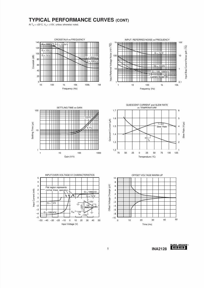
TYPICAL PERFORMANCE CURVES (CONT)At TA = +25 °C, V S = ±15V, unless otherwise noted.
CROSSTALK vs FREQUENCY
Frequency (Hz)
C r o s s
t a l k ( d B )
10 100 10k 1M1k
140
120
100
80
60
40
20
0100k
G = 1V/V
G = 10V/V
G = 100V/VG = 1000V/V
G = 1000V/V
G = 100V/V
SETTLING TIME vs GAIN
Gain (V/V)
S e
t t l i n g
T i m e
( µ s
)
100
10
11 10 100 1000
0.01%
0.1%
OFFSET VOLTAGE WARM-UP10
8
6
4
2
0
–2 –4
–6
–8
–100 10 20 30 40 50
Time (ms)
O f f s e t V o l t a g e
C h a n g e
( µ V )
INPUT OVER-VOLTAGE V/I CHARACTERISTICS5
4
3
2
1
0
–1 –2
–3
–4
–5
I n p u t
C u r r e n
t ( m A )
Input Voltage (V)
–50 –40 –30 –20 –10 10 20 30 400 50
G = 1V/V
G = 1V/V
G = 1000V/V
G = 1000V/V VINIIN –15V
+15V
INA21281/2
Flat region representsnormal linear operation.
INPUT- REFERRED NOISE vs FREQUENCY
Frequency (Hz)
I n p u
t - R e
f e r r e
d V o
l t a g e
N o
i s e ( n V / √
H z
)
1 10 1k100
1k
100
10
110k
G = 1V/V
G = 10V/V
100
10
1
0.1
I n p u
t B i a s
C u r r e n
t N o
i s e ( p A /
√ H
z )
Current Noise
G = 100, 1000V/V
QUIESCENT CURRENT and SLEW RATEvs TEMPERATURE
Temperature (°C)
Q u
i e s c e n
t C u r r e n
t ( µ A )
1.7
1.6
1.5
1.4
1.3
1.2
6
5
4
3
2
1 –75 –50 –25 0 25 50 75 100 125
S l e w
R a
t e ( V / µ s
)
IQ
Slew Rate

8/6/2019 In a 2128
http://slidepdf.com/reader/full/in-a-2128 6/12
®
INA2128 6
TYPICAL PERFORMANCE CURVES (CONT)At TA = +25 °C, V S = ±15V, unless otherwise noted.
MAXIMUM OUTPUT VOLTAGE vs FREQUENCY
Frequency (Hz)
P e a
k - t o - P e a k
O u
t p u
t V o
l t a g e
( V p p
)30
25
20
15
10
5
01k 10k 100k 1M
G = 1
G = 10, 100
G = 1000
SHORT-CIRCUIT OUTPUT CURRENTvs TEMPERATURE
16
14
12
10
8
6
4
2
0 –75 –50 –25 0 25 50 75 100 125
Temperature (°C)
S h o r t C i r c u i t C u r r e n
t ( m A )
–ISC
+ISC
OUTPUT VOLTAGE SWINGvs OUTPUT CURRENT
(V+)
(V+)–0.4
(V+)–0.8
(V+)–1.2
(V+)+1.2
(V–)+0.8
(V–)+0.4
V– 0 1 2 3 4
Output Current (mA)
O u
t p u
t V o
l t a g e
( V )
OUTPUT VOLTAGE SWINGvs POWER SUPPLY VOLTAGE
V+
(V+)–0.4
(V+)–0.8
(V+)–1.2
(V–)+1.2
(V–)+0.8
(V–)+0.4
V– 0 5 10 15 20
Power Supply Voltage (V)
O u t p u t V o l t a g e
S w
i n g ( V )
+25°C +85°C
–40°C
+25°C –40°C
+85°C
RL = 10k Ω
+85°C –40°C
INPUT BIAS CURRENT vs TEMPERATURE2
1
0
–1
–2
–75 –50 –25 0 25 50 75 100 125
Temperature (°C)
I n p u t B i a s C u r r e n t ( n A )
IOS
IB
Typical I B and I OSRange ±2nA at 25°C
TOTAL HARMONIC DISTORTION + NOISEvs FREQUENCY
Frequency (Hz)
T H
D +
N ( % )
100 1k 10k
1
0.1
0.01
0.001100k
VO = 1Vrms G = 1RL = 10k Ω
G = 10V/VRL = 100k Ω
G = 100, R L = 100k Ω
G = 1, R L = 100k Ω
500kHz MeasurementBandwidth
Dashed Portionis noise limited.
8/6/2019 In a 2128
http://slidepdf.com/reader/full/in-a-2128 7/12
®
INA21287
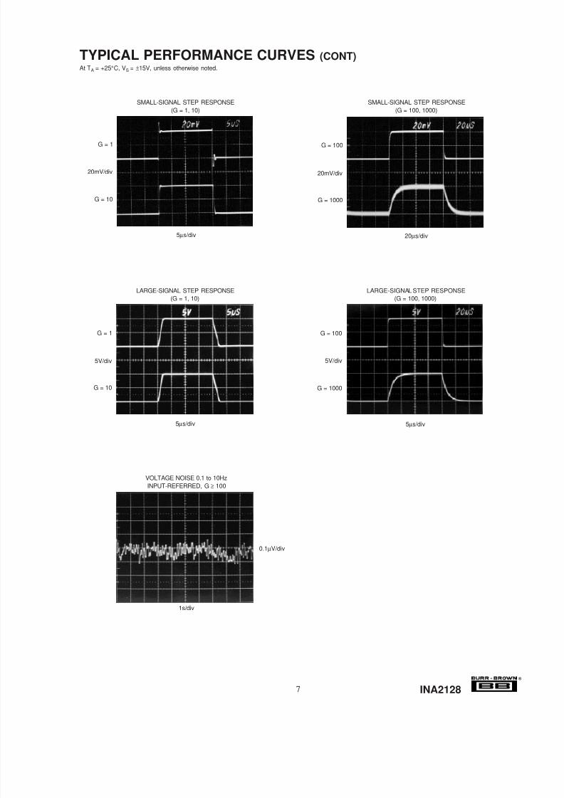
TYPICAL PERFORMANCE CURVES (CONT)At TA = +25 °C, V S = ±15V, unless otherwise noted.
G = 1
G = 10
5µs/div
SMALL-SIGNAL STEP RESPONSE(G = 1, 10)
G = 100
G = 1000
20 µs/div
SMALL-SIGNAL STEP RESPONSE(G = 100, 1000)
G = 1
G = 10
5µs/div
LARGE-SIGNAL STEP RESPONSE(G = 1, 10)
G = 100
G = 1000
5µs/div
LARGE-SIGNAL STEP RESPONSE(G = 100, 1000)
0.1 µV/div
1s/div
VOLTAGE NOISE 0.1 to 10HzINPUT-REFERRED, G ≥ 100
20mV/div 20mV/div
5V/div5V/div

8/6/2019 In a 2128
http://slidepdf.com/reader/full/in-a-2128 8/12
8/6/2019 In a 2128
http://slidepdf.com/reader/full/in-a-2128 9/12
®
INA21289
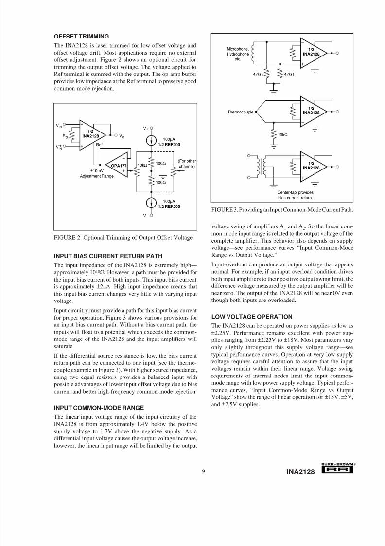
OFFSET TRIMMINGThe INA2128 is laser trimmed for low offset voltage andoffset voltage drift. Most applications require no externaloffset adjustment. Figure 2 shows an optional circuit fortrimming the output offset voltage. The voltage applied toRef terminal is summed with the output. The op amp bufferprovides low impedance at the Ref terminal to preserve goodcommon-mode rejection.
FIGURE 3. Providing an Input Common-Mode Current Path.
voltage swing of amplifiers A 1 and A 2. So the linear com-mon-mode input range is related to the output voltage of thecomplete amplifier. This behavior also depends on supplyvoltage—see performance curves “Input Common-ModeRange vs Output Voltage.”
Input-overload can produce an output voltage that appearsnormal. For example, if an input overload condition drivesboth input amplifiers to their positive output swing limit, the
difference voltage measured by the output amplifier will benear zero. The output of the INA2128 will be near 0V eventhough both inputs are overloaded.
LOW VOLTAGE OPERATIONThe INA2128 can be operated on power supplies as low as±2.25V. Performance remains excellent with power sup-plies ranging from ±2.25V to ±18V. Most parameters varyonly slightly throughout this supply voltage range—seetypical performance curves. Operation at very low supplyvoltage requires careful attention to assure that the inputvoltages remain within their linear range. Voltage swingrequirements of internal nodes limit the input common-
mode range with low power supply voltage. Typical perfor-mance curves, “Input Common-Mode Range vs OutputVoltage” show the range of linear operation for ±15V, ±5V,and ±2.5V supplies.
47k Ω47k Ω
10k Ω
Microphone,Hydrophone
etc.
Thermocouple
Center-tap providesbias current return.
INA21281/2
INA21281/2
INA21281/2
10k ΩOPA177
±10mVAdjustment Range
100 Ω (For otherchannel)
100 Ω
100µA1/2 REF200
100µA1/2 REF200
V+
V–
RG INA21281/2
Ref
VO
VIN –
VIN+
FIGURE 2. Optional Trimming of Output Offset Voltage.
INPUT BIAS CURRENT RETURN PATHThe input impedance of the INA2128 is extremely high—approximately 10 10Ω. However, a path must be provided forthe input bias current of both inputs. This input bias current
is approximately ±2nA. High input impedance means thatthis input bias current changes very little with varying inputvoltage.
Input circuitry must provide a path for this input bias currentfor proper operation. Figure 3 shows various provisions foran input bias current path. Without a bias current path, theinputs will float to a potential which exceeds the common-mode range of the INA2128 and the input amplifiers willsaturate.
If the differential source resistance is low, the bias currentreturn path can be connected to one input (see the thermo-couple example in Figure 3). With higher source impedance,using two equal resistors provides a balanced input withpossible advantages of lower input offset voltage due to biascurrent and better high-frequency common-mode rejection.
INPUT COMMON-MODE RANGEThe linear input voltage range of the input circuitry of theINA2128 is from approximately 1.4V below the positivesupply voltage to 1.7V above the negative supply. As adifferential input voltage causes the output voltage increase,however, the linear input range will be limited by the output

8/6/2019 In a 2128
http://slidepdf.com/reader/full/in-a-2128 10/12
®
INA2128 10
INPUT PROTECTIONThe inputs of the INA2128 are individually protected forvoltages up to ±40V. For example, a condition of –40V onone input and +40V on the other input will not causedamage. Internal circuitry on each input provides low seriesimpedance under normal signal conditions. To provideequivalent protection, series input resistors would contributeexcessive noise. If the input is overloaded, the protection
circuitry limits the input current to a safe value of approxi-mately 1.5 to 5mA. The typical performance curve “InputBias Current vs Common-Mode Input Voltage” shows thisinput current limit behavior. The inputs are protected even if the power supplies are disconnected or turned off.
CHANNEL CROSSTALKThe two channels of the INA2128 are completely indepen-dent, including all bias circuitry. At DC and low frequencythere is virtually no signal coupling between channels.Crosstalk increases with frequency and is dependent oncircuit gain, source impedance and signal characteristics.
As source impedance increases, careful circuit layout willhelp achieve lowest channel crosstalk. Most crossstalk isproduced by capacitive coupling of signals from one channelto the input section of the other channel. To minimizecoupling, separate the input traces as far as practical fromany signals associated with the opposite channel. A groundedguard trace surrounding the inputs helps reduce stray cou-pling between channels. Run the differential inputs of eachchannel parallel to each other or directly adjacent on top andbottom side of a circuit board. Stray coupling then tends toproduce a common-mode signal which is rejected by theIA’s input.
FIGURE 5. Sum of Differences Amplifier.FIGURE 4. Two-Axis Bridge Amplifier.
FIGURE 6. ECG Amplifier With Right-Leg Drive.
INA21281/2
RG /2
RG = 5.6k Ω
VOLA
RL
RA
10k Ω
Ref
NOTE: Due to the INA2128’s current-feedbacktopology, V G is approximately 0.7V less thanthe common-mode input voltage. This DC offsetin this guard potential is satisfactory for manyguarding applications.
G = 102.8k Ω
VGVG
2.8k Ω
1/2OPA2604
390k Ω
390k Ω
1/2OPA2604
VO = G A (V2 – V1) + G B (V4 – V3)V1
V2
Ref
V3
RGB
RGA
V4
Ref
INA21281/2
INA21281/2
X-axisVO
Y-axisVO
X-axis
Y-axis
VEX
VEX
INA21281/2
INA21281/2
8/6/2019 In a 2128
http://slidepdf.com/reader/full/in-a-2128 11/12
IMPORTANT NOTICE
Texas Instruments and its subsidiaries (TI) reserve the right to make changes to their products or to discontinueany product or service without notice, and advise customers to obtain the latest version of relevant informationto verify, before placing orders, that information being relied on is current and complete. All products are soldsubject to the terms and conditions of sale supplied at the time of order acknowledgment, including thosepertaining to warranty, patent infringement, and limitation of liability.
TI warrants performance of its semiconductor products to the specifications applicable at the time of sale inaccordance with TI’s standard warranty. Testing and other quality control techniques are utilized to the extentTI deems necessary to support this warranty. Specific testing of all parameters of each device is not necessarilyperformed, except those mandated by government requirements.
Customers are responsible for their applications using TI components.
In order to minimize risks associated with the customer’s applications, adequate design and operatingsafeguards must be provided by the customer to minimize inherent or procedural hazards.
TI assumes no liability for applications assistance or customer product design. TI does not warrant or representthat any license, either express or implied, is granted under any patent right, copyright, mask work right, or otherintellectual property right of TI covering or relating to any combination, machine, or process in which such
semiconductor products or services might be or are used. TI’s publication of information regarding any thirdparty’s products or services does not constitute TI’s approval, warranty or endorsement thereof.
Copyright © 2000, Texas Instruments Incorporated

8/6/2019 In a 2128
http://slidepdf.com/reader/full/in-a-2128 12/12
This datasheet has been download from:
www.datasheetcatalog.com
Datasheets for electronics components.