improving the power cycling performance of the emitter ... · improving the power cycling...
TRANSCRIPT
Microelectronics Reliability 54 (2014) 2796–2800
Contents lists available at ScienceDirect
Microelectronics Reliability
journal homepage: www.elsevier .com/locate /microrel
Improving the power cycling performance of the emitter contactof IGBT modules: Implementation and evaluation of stitch bond layouts
http://dx.doi.org/10.1016/j.microrel.2014.08.0150026-2714/� 2014 Elsevier Ltd. All rights reserved.
⇑ Corresponding author.E-mail address: [email protected] (E. Özkol).
Emre Özkol ⇑, Samuel Hartmann, Gontran PâquesABB Semiconductors, Lenzburg, Switzerland
a r t i c l e i n f o
Article history:Received 7 May 2014Received in revised form 6 August 2014Accepted 19 August 2014Available online 12 September 2014
Keywords:Power cyclingIGBTReliabilityWirebond layoutFEM
a b s t r a c t
The emitter (front metallization) of IGBTs is contacted by wire bonding. In this study, the influence of thewirebond layout on the power cycling performance of IGBT modules is investigated. Stitch bonding isimplemented to modify the wirebond layout of the emitter contact. The different layouts are subjectedto power cycling tests. For a better understanding of the experimental results, electrical and thermo-mechanical FEM simulations are run and the current distribution and induced mechanical stress isdiscussed. Based on the results of this study, the emitter contact of the new HiPak module platform isdesigned.
� 2014 Elsevier Ltd. All rights reserved.
1. Introduction
The HiPak IGBT power module platform (insulated gate bipolartransistor and diode modules) covering a broad matrix of voltage(up to 6.5 kV) and current (up to 3.6 kA) is a perfect choice for highpower applications including traction, industrial drives as well asrenewable energy (wind, solar).
The high power is achieved by the parallel connection of semi-conductor chips, typically up to 12 diodes and 24 IGBTs. The powermodule package provides a mechanical protection of the chips, anefficient transfer of the heat generated due to power losses as wellas an electrical isolation of the power circuit from the heat sink.Inside the module, the chips are soldered on a metallized ceramicsubstrate, which is soldered on a baseplate. The conductor leads(terminals) are also soldered on the metallization of the substrate.The emitter contact of the chips (top surface) is bonded to the sub-strate via wedge wire bonding. A simple sketch of the module’sinterior with the respective joints is depicted in Fig. 1.
In application, the power modules are subjected to temperaturecycles, which cause severe thermo-mechanical stress particularlyat the joints between different components of the module(Fig. 1). The modules degrade gradually in the field and finally faildue to the degradation of the weakest joint, which is specific to theapplication. Improving the affected joint, increases the overalllifetime.
This article focuses on the improvement of the emitter contactof the chips against thermo-mechanical stress induced by temper-ature cycles. A novel technique for reinforcing the emitter contactis to replace the Al-wirebonds with Cu-wirebonds [1–3], with Al-clad Cu-wirebonds [4], with novel Al-alloys [5–7], or with a flexiblecircuit board sintered on the chip surface [8]. Such techniques arebeneficial for improving the durability of the emitter contact, buton the other hand they require expensive and complex bondingand plating processes. A more practical approach is to improveand optimize the classical Al-wirebond emitter contact. For thispurpose, either the front metallization of the chip can be improved[7,9,10] or the layout of the Al-wirebond pattern [7,11,12].
Generally, power cycling tests are applied as a measure of thereliability of the emitter contact [2–4]. In these tests, the emittercontact is repetitively subjected to identical temperature cyclesuntil failure. The total number of cycles until failure is defined asthe power cycling capability. The higher the power cycling capabil-ity, the more durable and reliable is the emitter contact.
In this study, different wirebond layouts of the emitter contactof the IGBTs were implemented. The layouts were diversifiedmainly by introducing stitch bonds. The different emitter contactswere power cycled in order to investigate and determine the influ-ence of the layout on the power cycling capability. For a betterunderstanding of the experimental results, simplified models weresimulated using finite element method (FEM) and the temperatureand current density distributions at the emitter contacts werecomputed. As a result, an emitter contact was developed, whichhas a 4 times higher power cycling capability of the current emitter

Fig. 1. A simple sketch of the internal structure of a power module.
E. Özkol et al. / Microelectronics Reliability 54 (2014) 2796–2800 2797
contact. This emitter contact is implemented in the new HiPakmodule platform with improved reliability [12].
2. Experimental
2.1. State of the art – power cycling capability of the current emittercontact
The power cycling capability of the current HiPak module plat-form is given in detail in an ABB application note [13]. There, sep-arate graphs show the 10% lifetime capability (B10-lifetime) curvesof each joint. The B10-lifetime curves of the emitter contact (thelifetime curves of the wirebond joint) are given for a maximumjunction temperature (Tj,max) of 75–175 �C. The power cyclingcapability of the emitter contact depends on the number/type/form/layout of the wirebonds on the chips. Such properties differfrom module to module considering the entire HiPak module plat-form. Thus, the reader should consider that the lifetime curves inthe application note [13] show the critical lifetime curves for allmodules of the platform.
2.2. The investigated emitter contact designs
The design of experiments included totally 4 different wirebondlayouts including the reference layout. In all samples the 6.5 kVABB IGBTs (nominal current rating of 31 A) were connected 8 timeswith a 15 mil Al-wire per IGBT. In 3 of the 4 layouts, stitch bondswere implemented. A stitch bond can be defined as a wirebondwith more than one bond contact on the same chip, whereas anormal wirebond has only 2 bond contacts, one on the chip andthe other on the substrate (Fig. 2). The 4 different wirebond layoutscan be listed as ‘‘reference’’ with standard wirebond layout withoutstitch-bonds, ‘‘short-stitch’’ where the short wires are stitch-bonded, ‘‘long-stitch’’ where the long wires are stitch-bonded,and ‘‘all-stitch’’ where all wires are stitch-bonded.
The FEM-models of the reference layout without stitch bondsand the short-stitch layout where the short wires arestitch-bonded are given in Fig. 2. The models are realistic and inaccordance with the cycled samples in terms of number of bonds,wirebond layout, loop shape, etc.
Fig. 2. (a) Short-stitch and (b) standard layouts. Figure
2.3. Power cycling tests
HiPak modules were built with the corresponding IGBTs andpower cycling tests were performed. The testing parameters wereset to achieve a temperature swing of Tj: 100–170 �C:
� tcycle = 0.73 s with a 50% duty cycle.� IIGBT = �60 A.
Each module was individually cooled to regulate the Tj,max at170 �C during the test. The gate voltage of all modules was 15 Vduring the test.
The Tj of the modules was determined using the VCE(T)-method[14]. The Tj and VCE values (collector emitter voltage) of themodules were measured several times a day.
The modules were power cycled until the failure criteria, whichis defined as a 5% increase in the VCE or a short between gate andemitter occured. The results of the power cycling tests wasstatistically evaluated by fitting the failure data to Weibullstatistics using the maximum likelihood estimation method(Minitab 16 Statistical Software).
3. FEM simulations
In order to better understand the experimentally obtaineddifferences in the power cycling performances, two differentlayouts are simulated using the finite element software COMSOLMultiphysics.
The geometry of the wire bonds is modelled according to thereal shape of the tested samples. The chip is modelled with an alu-minum metallisation of 4 lm thickness and assuming a resistivematerial in the active volume of the chip. The electrical conductiv-ity of the chip material is set to match the expected voltage dropaccording to the chip’s data sheet. Further geometric elementsmodelled are: chip solder, the ceramic substrate with its top andbottom metallisation, the substrate solder, the base plate and thecooler. The thermal interface between the module’s base plateand the cooler is modelled with a heat transfer coefficient of6500 W/(m2 K) according to a measurement on the test equipment.Also transition from the cooler to the cooling water at 30 �C ismodelled with a heat transfer coefficient. This is set to 3300 W/(m2 K) to achieve an average junction temperature of 135 �C as inthe experiment.
In a first step the electric current distribution is calculated. Theresistive power loss density from the electric simulation result istaken as input for a transient thermal simulation. By turning onand off the heat source, the thermal cycling is simulated in a sec-ond step. The average temperature distribution from a steady statethermal simulation is used as initial condition. This enabled reach-ing a realistic periodic state after only 10 cycles of transientsimulation.
shows the mesh used in the finite element model.

Fig. 3. SEM image of a typical wirebond lift-off.
2798 E. Özkol et al. / Microelectronics Reliability 54 (2014) 2796–2800
In a third step the mechanical simulation is done. Althoughmaterial fatigue due to cyclic plastic deformation of the materialis assumed to be the failure mechanism, the simulation is donepurely elastic to keep the numeric effort reasonably low. It isassumed that the material is stress free at a certain averagetemperature distribution. For that the average is taken of thetemperature fields at the start and the end of heating cycle. Themechanical deformation is then calculated when going from thisstress free temperature field to the temperature field at the endof the heating cycle. As a result the elastic deformation and stressamplitude is obtained.
In reality above a yield strength between 15 MPa and 30 MPa,depending on wire bond material and temperature, the materialwill deform plastically [17]. The magnitude of the elastic stressamplitude from the simulation is expected to be strongly relatedto the amount of plastic deformation the material undergoes percycle in the real experiment and thus related with the powercycling life time.
4. Results and discussion
4.1. Results from power cycling
The results of the power cycling tests are summarized in Table 1.The total cycles until failure of all samples are listed. Totally 6 sam-ples with the reference layout, 3 samples each with short-stitchand long-stitch layouts, and 4 samples with all-stitch layout weretested until failure. The observed cycles until failure was 2–3 timeshigher for the stitch bonded samples in comparison to the refer-ence samples. The failure mode of the reference samples was aGE-short while it was a 5% increase in VCE for the stitch bondedsamples.
During power cycling the VCE of all modules increases steadily.The increase is due to the reconstruction of the front metallizationof the IGBTs as well as the detachment of the wirebonds (lift-off). Agradual lift off of the wirebonds means that the connecting wire-bonds commute higher currents. This could result in a mechanicaldamage of the chip, which forms a GE-short during power cyclingdue to a local hotspot around the not lifted wirebonds [7]. The VCE
curves of the reference samples showed a parabolic increase.Extrapolating these VCE curves showed that the modules wouldapproximately reach the 5% VCE limit at the moment of theGE-short. Thus, the failure mode of the reference and stitch bondedsamples can be considered to be comparable, which allows theevaluation of the results by Weibull statistics.
Table 1Summary of the power cycling tests.
Sample Power cycling results
Type Cycles until failure
R1 Reference 1,490,000R2 Reference 1,350,000R3 Reference 2,425,000R4 Reference 1,600,000R5 Reference 1,135,000R6 Reference 1,300,000S1 Short-stitch 3,310,000S2 Short-stitch 3,760,000S3 Short-stitch 3,840,000L1 Long-stitch 3,070,000L2 Long-stitch 2,490,000L3 Long-stitch 4,470,000A1 All-stitch 5,310,000A2 All-stitch 5,005,000A3 All-stitch 3,280,000A4 All-stitch 3,520,000
Moreover, a few modules of all types were opened after thepower cycling tests. All other components were removed in orderto analyze the wirebond joints. It was observed that about 3/4thof all wirebonds were lifted independently of the type of layout.Scanning electron microscopic (SEM) analysis showed that thelift-offs occur due to a crack in the wirebond as shown in Fig. 3.The SEM image belongs to the short-stitch module S1, which wassubjected to 3.3 M cycles. The bond pad of the lifted wirebondsare comparable to each other and thus we can say that the imagein Fig. 3 is representative for the lift-off phenomenon in general.
During power cycling, other joints than the wirebonds are alsoaging and degrading. For the given cycling conditions, the dieattach may degrade as well. In order to investigate the state ofthe die attach after cycling the modules R1 and S1 are analyzedby scanning acoustic microscopy (SAM). The SAM-images inFig. 4 shows the die attach of the modules after power cycling.The r1 was directly removed from the testing equipment afterend of life, however the S1 was further cycled for 0.6 M cycles untilit was removed, which means the SAM-image shows the state ofthe die attach of the module S1 after totally �3.9 M cycles. Theimages show each 2 substrates of the modules and the centralfor chips are the diodes and the rest 8 chips are the IGBTs. Typicallyin SAM-images whitish colors in the given level indicate solder
Fig. 4. SAM images of the die attach of the modules (a) R1 and (b) S1 after powercycling.
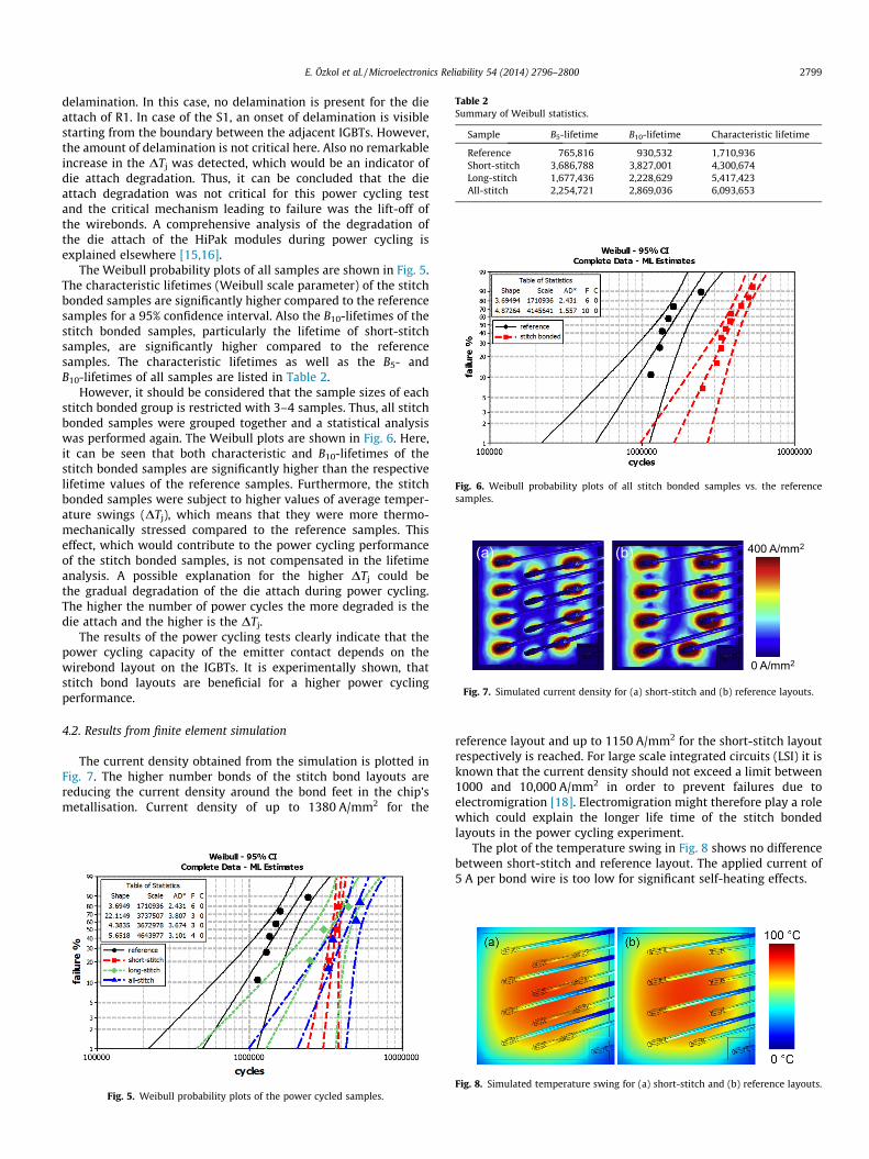
Table 2Summary of Weibull statistics.
Sample B5-lifetime B10-lifetime Characteristic lifetime
Reference 765,816 930,532 1,710,936Short-stitch 3,686,788 3,827,001 4,300,674Long-stitch 1,677,436 2,228,629 5,417,423All-stitch 2,254,721 2,869,036 6,093,653
Fig. 6. Weibull probability plots of all stitch bonded samples vs. the referencesamples.
400 A/mm2
0 A/mm2
(a) (b)
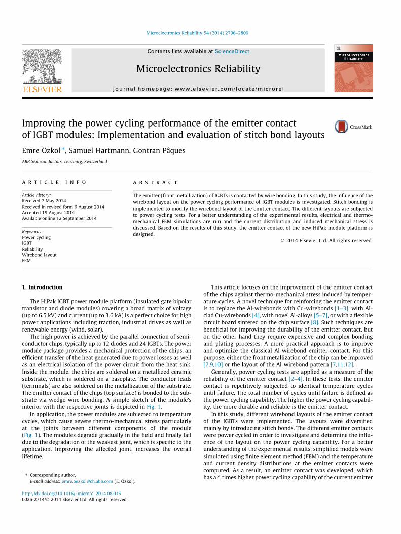
Fig. 7. Simulated current density for (a) short-stitch and (b) reference layouts.
E. Özkol et al. / Microelectronics Reliability 54 (2014) 2796–2800 2799
delamination. In this case, no delamination is present for the dieattach of R1. In case of the S1, an onset of delamination is visiblestarting from the boundary between the adjacent IGBTs. However,the amount of delamination is not critical here. Also no remarkableincrease in the DTj was detected, which would be an indicator ofdie attach degradation. Thus, it can be concluded that the dieattach degradation was not critical for this power cycling testand the critical mechanism leading to failure was the lift-off ofthe wirebonds. A comprehensive analysis of the degradation ofthe die attach of the HiPak modules during power cycling isexplained elsewhere [15,16].
The Weibull probability plots of all samples are shown in Fig. 5.The characteristic lifetimes (Weibull scale parameter) of the stitchbonded samples are significantly higher compared to the referencesamples for a 95% confidence interval. Also the B10-lifetimes of thestitch bonded samples, particularly the lifetime of short-stitchsamples, are significantly higher compared to the referencesamples. The characteristic lifetimes as well as the B5- andB10-lifetimes of all samples are listed in Table 2.
However, it should be considered that the sample sizes of eachstitch bonded group is restricted with 3–4 samples. Thus, all stitchbonded samples were grouped together and a statistical analysiswas performed again. The Weibull plots are shown in Fig. 6. Here,it can be seen that both characteristic and B10-lifetimes of thestitch bonded samples are significantly higher than the respectivelifetime values of the reference samples. Furthermore, the stitchbonded samples were subject to higher values of average temper-ature swings (DTj), which means that they were more thermo-mechanically stressed compared to the reference samples. Thiseffect, which would contribute to the power cycling performanceof the stitch bonded samples, is not compensated in the lifetimeanalysis. A possible explanation for the higher DTj could bethe gradual degradation of the die attach during power cycling.The higher the number of power cycles the more degraded is thedie attach and the higher is the DTj.
The results of the power cycling tests clearly indicate that thepower cycling capacity of the emitter contact depends on thewirebond layout on the IGBTs. It is experimentally shown, thatstitch bond layouts are beneficial for a higher power cyclingperformance.
4.2. Results from finite element simulation
The current density obtained from the simulation is plotted inFig. 7. The higher number bonds of the stitch bond layouts arereducing the current density around the bond feet in the chip’smetallisation. Current density of up to 1380 A/mm2 for the
Fig. 5. Weibull probability plots of the power cycled samples.
reference layout and up to 1150 A/mm2 for the short-stitch layoutrespectively is reached. For large scale integrated circuits (LSI) it isknown that the current density should not exceed a limit between1000 and 10,000 A/mm2 in order to prevent failures due toelectromigration [18]. Electromigration might therefore play a rolewhich could explain the longer life time of the stitch bondedlayouts in the power cycling experiment.
The plot of the temperature swing in Fig. 8 shows no differencebetween short-stitch and reference layout. The applied current of5 A per bond wire is too low for significant self-heating effects.
Fig. 8. Simulated temperature swing for (a) short-stitch and (b) reference layouts.
100 MPa
0 MPa
(a) (b)
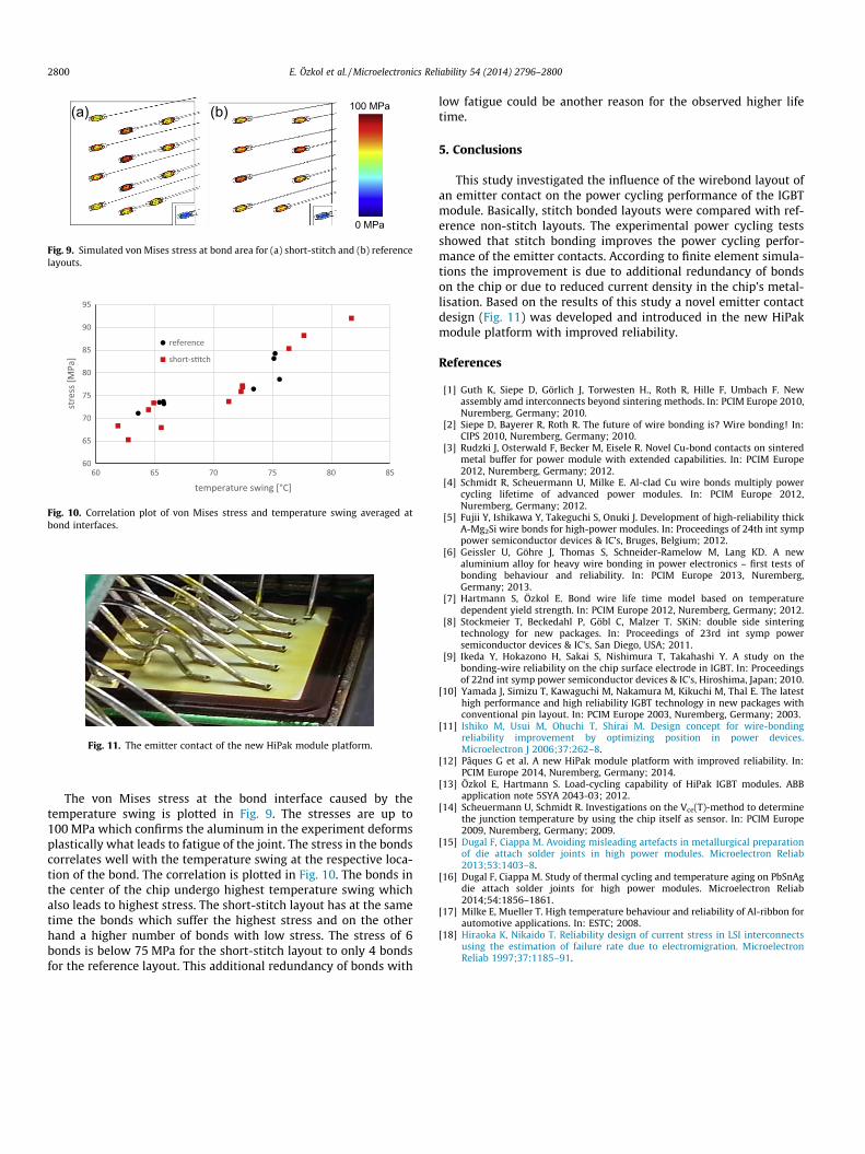
Fig. 9. Simulated von Mises stress at bond area for (a) short-stitch and (b) referencelayouts.
60
65
70
75
80
85
90
95
60 65 70 75 80 85
stre
ss [M
Pa]
temperature swing [°C]
reference
short-s�tch
Fig. 10. Correlation plot of von Mises stress and temperature swing averaged atbond interfaces.
Fig. 11. The emitter contact of the new HiPak module platform.
2800 E. Özkol et al. / Microelectronics Reliability 54 (2014) 2796–2800
The von Mises stress at the bond interface caused by thetemperature swing is plotted in Fig. 9. The stresses are up to100 MPa which confirms the aluminum in the experiment deformsplastically what leads to fatigue of the joint. The stress in the bondscorrelates well with the temperature swing at the respective loca-tion of the bond. The correlation is plotted in Fig. 10. The bonds inthe center of the chip undergo highest temperature swing whichalso leads to highest stress. The short-stitch layout has at the sametime the bonds which suffer the highest stress and on the otherhand a higher number of bonds with low stress. The stress of 6bonds is below 75 MPa for the short-stitch layout to only 4 bondsfor the reference layout. This additional redundancy of bonds with
low fatigue could be another reason for the observed higher lifetime.
5. Conclusions
This study investigated the influence of the wirebond layout ofan emitter contact on the power cycling performance of the IGBTmodule. Basically, stitch bonded layouts were compared with ref-erence non-stitch layouts. The experimental power cycling testsshowed that stitch bonding improves the power cycling perfor-mance of the emitter contacts. According to finite element simula-tions the improvement is due to additional redundancy of bondson the chip or due to reduced current density in the chip’s metal-lisation. Based on the results of this study a novel emitter contactdesign (Fig. 11) was developed and introduced in the new HiPakmodule platform with improved reliability.
References
[1] Guth K, Siepe D, Görlich J, Torwesten H., Roth R, Hille F, Umbach F. Newassembly amd interconnects beyond sintering methods. In: PCIM Europe 2010,Nuremberg, Germany; 2010.
[2] Siepe D, Bayerer R, Roth R. The future of wire bonding is? Wire bonding! In:CIPS 2010, Nuremberg, Germany; 2010.
[3] Rudzki J, Osterwald F, Becker M, Eisele R. Novel Cu-bond contacts on sinteredmetal buffer for power module with extended capabilities. In: PCIM Europe2012, Nuremberg, Germany; 2012.
[4] Schmidt R, Scheuermann U, Milke E. Al-clad Cu wire bonds multiply powercycling lifetime of advanced power modules. In: PCIM Europe 2012,Nuremberg, Germany; 2012.
[5] Fujii Y, Ishikawa Y, Takeguchi S, Onuki J. Development of high-reliability thickA-Mg2Si wire bonds for high-power modules. In: Proceedings of 24th int symppower semiconductor devices & IC’s, Bruges, Belgium; 2012.
[6] Geissler U, Göhre J, Thomas S, Schneider-Ramelow M, Lang KD. A newaluminium alloy for heavy wire bonding in power electronics – first tests ofbonding behaviour and reliability. In: PCIM Europe 2013, Nuremberg,Germany; 2013.
[7] Hartmann S, Özkol E. Bond wire life time model based on temperaturedependent yield strength. In: PCIM Europe 2012, Nuremberg, Germany; 2012.
[8] Stockmeier T, Beckedahl P, Göbl C, Malzer T. SKiN: double side sinteringtechnology for new packages. In: Proceedings of 23rd int symp powersemiconductor devices & IC’s, San Diego, USA; 2011.
[9] Ikeda Y, Hokazono H, Sakai S, Nishimura T, Takahashi Y. A study on thebonding-wire reliability on the chip surface electrode in IGBT. In: Proceedingsof 22nd int symp power semiconductor devices & IC’s, Hiroshima, Japan; 2010.
[10] Yamada J, Simizu T, Kawaguchi M, Nakamura M, Kikuchi M, Thal E. The latesthigh performance and high reliability IGBT technology in new packages withconventional pin layout. In: PCIM Europe 2003, Nuremberg, Germany; 2003.
[11] Ishiko M, Usui M, Ohuchi T, Shirai M. Design concept for wire-bondingreliability improvement by optimizing position in power devices.Microelectron J 2006;37:262–8.
[12] Pâques G et al. A new HiPak module platform with improved reliability. In:PCIM Europe 2014, Nuremberg, Germany; 2014.
[13] Özkol E, Hartmann S. Load-cycling capability of HiPak IGBT modules. ABBapplication note 5SYA 2043-03; 2012.
[14] Scheuermann U, Schmidt R. Investigations on the Vce(T)-method to determinethe junction temperature by using the chip itself as sensor. In: PCIM Europe2009, Nuremberg, Germany; 2009.
[15] Dugal F, Ciappa M. Avoiding misleading artefacts in metallurgical preparationof die attach solder joints in high power modules. Microelectron Reliab2013;53:1403–8.
[16] Dugal F, Ciappa M. Study of thermal cycling and temperature aging on PbSnAgdie attach solder joints for high power modules. Microelectron Reliab2014;54:1856–1861.
[17] Milke E, Mueller T. High temperature behaviour and reliability of Al-ribbon forautomotive applications. In: ESTC; 2008.
[18] Hiraoka K, Nikaido T. Reliability design of current stress in LSI interconnectsusing the estimation of failure rate due to electromigration. MicroelectronReliab 1997;37:1185–91.