improving the performance and reducing the consumption …webs.um.es/aflores/papers/thesis.pdf ·...
TRANSCRIPT

UNIVERSIDAD DE MURCIA
Departamento de Ingenierıa y Tecnologıa de Computadores
Improving the Performance and Redu-
cing the Consumption of Multicore Pro-
cessors using Heterogeneous Networks
A DISSERTATION
SUBMITTED IN FULFILLMENT OF THE REQUIREMENTS
FOR THE DEGREE OF
Doctor of Philosophy
By
Antonio Flores Gil
Advisors
Manuel Eugenio Acacio Sanchez
Juan Luis Aragon Alcaraz
Murcia, May 2010


UNIVERSIDAD DE MURCIA
Departamento de Ingenierıa y Tecnologıa de Computadores
Mejora del Rendimiento y Reduccion de
Consumo de los Procesadores Multi-
nucleo Usando Redes Heterogeneas
TESIS PROPUESTA PARA
LA OBTENCION DEL GRADO DE
Doctor en Informatica
Presentada por:
Antonio Flores Gil
Dirigida por:
Manuel Eugenio Acacio Sanchez
Juan Luis Aragon Alcaraz
Murcia, Mayo 2010


D. Manuel Eugenio Acacio Sanchez, Profesor Titular de Universidad del Area
de Arquitectura y Tecnologıa de Computadores en el Departamento de Ingenierıa
y Tecnologıa de Computadores
y
D. Juan Luis Aragon Alcaraz, Profesor Titular de Universidad del Area de
Arquitectura y Tecnologıa de Computadores en el Departamento de Ingenierıa y
Tecnologıa de Computadores
AUTORIZAN:
La presentacion de la Tesis Doctoral titulada ((Mejora del Rendimiento y
Reduccion de Consumo de los Procesadores Multinucleo Usando Redes Hete-
rogeneas)), realizada por D. Antonio Flores Gil, bajo su inmediata direccion y
supervision, y que presenta para la obtencion del grado de Doctor por la Univer-
sidad de Murcia.
En Murcia, a 28 de Junio de 2010.
Fdo: Dr. Manuel Eugenio Acacio Sanchez
Fdo: Dr. Juan Luis Aragon Alcaraz
Departamento de Ingenierıa y Tecnologıa de Computadores
Campus Universitario de Espinardo. 30100 Murcia
Tel. 868 884 665 – Fax 868 884 151 – www.um.es/ditec


D. Antonio Javier Cuenca Munoz, Profesor Titular de Universidad del Area
de Arquitectura y Tecnologıa de Computadores y Director del Departamento de
Ingenierıa y Tecnologıa de Computadores, INFORMA:
Que la Tesis Doctoral titulada ((Mejora del Rendimiento y Reduccion de Con-
sumo de los Procesadores Multinucleo Usando Redes Heterogeneas)), ha sido rea-
lizada por D. Antonio Flores Gil, bajo la inmediata direccion y supervision de
D. Manuel Eugenio Acacio Sanchez y de D. Juan Luis Aragon Alcaraz, y que el
Departamento ha dado su conformidad para que sea presentada ante la Comision
de Doctorado.
En Murcia, a 30 de Junio de 2010.
Fdo: Dr. Antonio Javier Cuenca Munoz
Departamento de Ingenierıa y Tecnologıa de Computadores
Campus Universitario de Espinardo. 30100 Murcia
Tel. 868 884 665 – Fax 868 884 151 – www.um.es/ditec


To the memory of my grandparents,
To Marita, my lovely wife,
To mum and dad.


Acknowledgements
Completing this thesis has by no means been an easy task for me.
However, the experience has been very good on the whole thanks to
the help of many people that deserve credit for the final result. At
least for the good parts. First, I would like to thank my advisors, Dr.
Juan Luis Aragon Alcaraz and Dr. Manuel Eugenio Acacio Sanchez
for having me as a PhD student for almost four years.
I have had the luck to perform this work at the Departamento de In-
genierıa y Tecnologıa de Computadores of the Universidad de Murcia.
All the members of the department have always been ready to help
me whenever I asked, and sometimes even before I asked. Amongst
them, I should mention especially Marıa Pilar Gonzalez Ferez, who
has helped me in everything. I have felt her support for all these
years of hard work. And when my strengths weakened, her words of
encouragement helped me to go on.
Finally, I would like to dedicate this dissertation to my wonderful
family. For their endless love, support and encouragement. Partic-
ularly to my understanding and patient wife, Marita, who did more
than her share around the house as I sat at the computer. Without
her support, and gentle prodding, this work would not be possible.
I must also thank my loving mother and father who have helped so
much and have given me their fullest support. Finally, I dedicate this
work to my beloved grandparents, Antonio, Josefa, Jose, and Rosario.
xi


Contents
0. Resumen de la Tesis 1
0.1. Introduccion . . . . . . . . . . . . . . . . . . . . . . . . . . . . . . 1
0.1.1. El Problema de las Comunicaciones Globales en las Arqui-
tecturas Tiled CMP . . . . . . . . . . . . . . . . . . . . . 6
0.1.1.1. La Implementacion de los Alambres en las Redes
Heterogeneas . . . . . . . . . . . . . . . . . . . . 7
0.2. Contribuciones de la Tesis . . . . . . . . . . . . . . . . . . . . . . 9
0.3. Entorno de Evaluacion . . . . . . . . . . . . . . . . . . . . . . . . 10
0.4. Redes Heterogeneas y Particion de Respuestas . . . . . . . . . . . 12
0.5. Redes Heterogeneas y Compresion de Direcciones . . . . . . . . . 21
0.6. Redes Heterogeneas y Prefetching Hardware Energeticamente Efi-
ciente . . . . . . . . . . . . . . . . . . . . . . . . . . . . . . . . . 27
0.7. Conclusiones y Vıas Futuras . . . . . . . . . . . . . . . . . . . . . 34
1. Introduction 39
1.1. Motivation and Foundations . . . . . . . . . . . . . . . . . . . . . 39
1.1.1. The Global Communication Problem in Tiled CMP Archi-
tectures . . . . . . . . . . . . . . . . . . . . . . . . . . . . 44
1.1.1.1. Wire Implementation in Heterogeneous Networks 45
1.1.2. Router Implementation in Heterogeneous Networks . . . . 50
1.2. Thesis Contributions . . . . . . . . . . . . . . . . . . . . . . . . . 53
1.3. Thesis Organization . . . . . . . . . . . . . . . . . . . . . . . . . . 54
2. The Sim-PowerCMP Simulator, Evaluation Methodology, and
Problem Statement 57
2.1. Introduction . . . . . . . . . . . . . . . . . . . . . . . . . . . . . . 57
2.2. Related Work . . . . . . . . . . . . . . . . . . . . . . . . . . . . . 58
2.3. The Sim-PowerCMP Simulator . . . . . . . . . . . . . . . . . . 59
2.3.1. Core Microarchitecture . . . . . . . . . . . . . . . . . . . . 61
2.3.2. Memory Hierarchy . . . . . . . . . . . . . . . . . . . . . . 64
2.3.3. Interconnection Network . . . . . . . . . . . . . . . . . . . 65
2.3.4. Sim-PowerCMP Power Model Overview . . . . . . . . . 67
xiii

CONTENTS
2.4. Validation of the Power Model of Sim-PowerCMP . . . . . . . . 68
2.5. Benchmarks . . . . . . . . . . . . . . . . . . . . . . . . . . . . . . 76
2.5.1. BARNES-HUT . . . . . . . . . . . . . . . . . . . . . . . . 77
2.5.2. EM3D . . . . . . . . . . . . . . . . . . . . . . . . . . . . . 78
2.5.3. FFT . . . . . . . . . . . . . . . . . . . . . . . . . . . . . . 79
2.5.4. LU . . . . . . . . . . . . . . . . . . . . . . . . . . . . . . . 79
2.5.5. MP3D . . . . . . . . . . . . . . . . . . . . . . . . . . . . . 79
2.5.6. OCEAN . . . . . . . . . . . . . . . . . . . . . . . . . . . . 80
2.5.7. RADIX . . . . . . . . . . . . . . . . . . . . . . . . . . . . 81
2.5.8. RAYTRACE . . . . . . . . . . . . . . . . . . . . . . . . . 81
2.5.9. UNSTRUCTURED . . . . . . . . . . . . . . . . . . . . . . 81
2.5.10. WATER-NSQ . . . . . . . . . . . . . . . . . . . . . . . . . 82
2.5.11. WATER-SPA . . . . . . . . . . . . . . . . . . . . . . . . . 82
2.5.12. Summary of Applications Used in Our Experiments . . . . 83
2.6. Evaluating the Energy-Efficiency of CMP Architectures . . . . . . 84
2.6.1. Classification of Messages in Tiled CMP Architectures . . 86
3. Heterogeneous Interconnects for Energy-Efficient Message Man-
agement in CMPs 93
3.1. Introduction . . . . . . . . . . . . . . . . . . . . . . . . . . . . . . 93
3.2. Related Work . . . . . . . . . . . . . . . . . . . . . . . . . . . . . 94
3.3. Efficient Message Management in Tiled CMPs . . . . . . . . . . . 96
3.3.1. Reply Partitioning for Decoupling Data Messages into Crit-
ical and Non-Critical Parts . . . . . . . . . . . . . . . . . . 96
3.3.2. Designing the Interconnect for Efficient Message Management100
3.4. Experimental Results . . . . . . . . . . . . . . . . . . . . . . . . . 101
3.4.1. Evaluation Methodology . . . . . . . . . . . . . . . . . . . 101
3.4.2. Simulation Results and Analysis . . . . . . . . . . . . . . . 102
3.4.2.1. Message Distribution in Heterogeneous Networks 102
3.4.2.2. Execution Time Results . . . . . . . . . . . . . . 103
3.4.2.3. Energy-Efficiency Results . . . . . . . . . . . . . 107
3.5. Sensitivity Analysis . . . . . . . . . . . . . . . . . . . . . . . . . . 108
3.5.1. Out-of-order/In-order Processors . . . . . . . . . . . . . . 108
xiv
CONTENTS
3.5.2. Link Bandwidth . . . . . . . . . . . . . . . . . . . . . . . . 108
3.5.3. Relative Latency of the Interconnect with Respect to the
L2 Cache . . . . . . . . . . . . . . . . . . . . . . . . . . . 109
3.5.4. Partial Reply Sub-block Size Effect . . . . . . . . . . . . . 110
3.6. Conclusions . . . . . . . . . . . . . . . . . . . . . . . . . . . . . . 112
4. Exploiting Address Compression and Heterogeneous Intercon-
nects for Efficient Message Management in Tiled CMPs 115
4.1. Introduction . . . . . . . . . . . . . . . . . . . . . . . . . . . . . . 115
4.2. Related Work . . . . . . . . . . . . . . . . . . . . . . . . . . . . . 116
4.3. Address Compression Schemes . . . . . . . . . . . . . . . . . . . . 117
4.4. Combining Address Compression and Heterogeneous Networks . . 121
4.4.1. Interconnect Design for Efficient Message Management . . 122
4.5. Experimental Results . . . . . . . . . . . . . . . . . . . . . . . . . 123
4.5.1. Simulation Results and Analysis . . . . . . . . . . . . . . . 123
4.6. Sensitivity Analysis . . . . . . . . . . . . . . . . . . . . . . . . . . 128
4.6.1. Out-of-order/In-order Processors . . . . . . . . . . . . . . 128
4.6.2. Link Bandwidth . . . . . . . . . . . . . . . . . . . . . . . . 129
4.6.3. Relative Latency of the Interconnect with Respect to the
L2 Cache . . . . . . . . . . . . . . . . . . . . . . . . . . . 130
4.7. Conclusions . . . . . . . . . . . . . . . . . . . . . . . . . . . . . . 131
5. Energy-Efficient Hardware Prefetching for CMPs using Hetero-
geneous Interconnects 133
5.1. Introduction . . . . . . . . . . . . . . . . . . . . . . . . . . . . . . 133
5.2. Related Work . . . . . . . . . . . . . . . . . . . . . . . . . . . . . 135
5.3. Hardware Prefetching . . . . . . . . . . . . . . . . . . . . . . . . . 135
5.4. A Proposal for Energy-Efficient Prefetching Management in Tiled
CMPs . . . . . . . . . . . . . . . . . . . . . . . . . . . . . . . . . 137
5.4.1. Classification of Messages in Tiled CMP Architectures with
Prefetching . . . . . . . . . . . . . . . . . . . . . . . . . . 137
5.4.2. Interconnect Design for Efficient Message Management . . 139
5.5. Simulation Results and Analysis . . . . . . . . . . . . . . . . . . . 140
5.6. Sensitivity Analysis . . . . . . . . . . . . . . . . . . . . . . . . . . 144
xv
CONTENTS
5.6.1. Out-of-order/In-order Processors . . . . . . . . . . . . . . 144
5.6.2. Link Bandwidth . . . . . . . . . . . . . . . . . . . . . . . . 146
5.6.3. Relative Latency of the Interconnect with Respect to the
L2 Cache . . . . . . . . . . . . . . . . . . . . . . . . . . . 147
5.7. Conclusions . . . . . . . . . . . . . . . . . . . . . . . . . . . . . . 148
6. Conclusions and Future Directions 149
6.1. Conclusions . . . . . . . . . . . . . . . . . . . . . . . . . . . . . . 149
6.2. Future Directions . . . . . . . . . . . . . . . . . . . . . . . . . . . 152
Bibliography 164
xvi

List of Figures
0.1. Evolucion de los parametros de numero de transistores integra-
dos, consumo, frecuencia de reloj y paralelismo a nivel de instruc-
cion (ILP) para diferentes microprocesadores a lo largo del tiempo
(source: D. Patterson, UC–Berkeley). . . . . . . . . . . . . . . . . 2
0.2. Arquitectura CMP de baldosa considerada a lo largo de la Tesis. . 5
0.3. Modelo de primer orden de un repetidor. . . . . . . . . . . . . . . 7
0.4. Utilizacion acumulada de las lıneas de cache (arriba) y espacio
de tiempo disponible para el desacoplamiento de los mensajes de
datos (abajo) para un CMP de 16 nucleos. . . . . . . . . . . . . . 14
0.5. Ejemplo de aplicacion de la tecnica Reply Partitioning. . . . . . . 16
0.6. Tiempo de ejecucion normalizado cuando se utiliza enlaces het-
erogeneos. . . . . . . . . . . . . . . . . . . . . . . . . . . . . . . . 17
0.7. Energıa normalizada consumida por los enlaces (arriba) y producto
energy-delay2 (abajo) para las configuraciones evaluadas. . . . . . 19
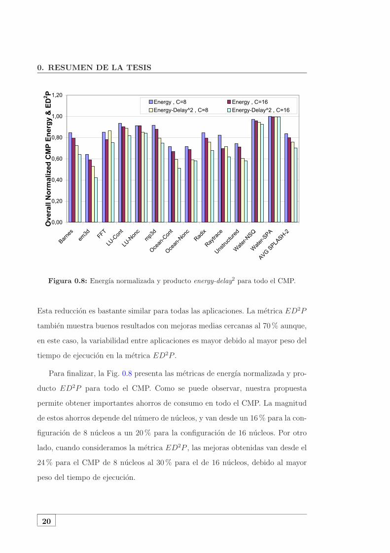
0.8. Energıa normalizada y producto energy-delay2 para todo el CMP. 20
0.9. Tiempo de ejecucion normalizado (arriba) y metrica ED2P de los
enlaces (abajo) para diferentes esquemas de compresion de direc-
ciones sobre enlaces heterogeneos (la anchura de los VL-Wires co-
incide con el tamano de las direcciones comprimidas). . . . . . . . 23
0.10. Tiempo de ejecucion normalizado (arriba) y metrica ED2P de los
enlaces (abajo) para diferentes esquemas de compresion de direc-
ciones sobre enlaces heterogeneos VL-Wires de 3 bytes de anchura
y fragmentacion de los mensajes. . . . . . . . . . . . . . . . . . . 25
0.11. Producto energy-delay2 (ED2P ) para la totalidad del CMP (con-
figuracion con VL-Wires de 3 bytes). . . . . . . . . . . . . . . . . 26
0.12. Tiempo de ejecucion normalizado y consumo de la red para un
CMP de 16 nucleos para distintas tecnicas de prefetching. . . . . . 27
0.13. Desglose de los mensajes que circulan a traves de la red de in-
terconexion para un CMP de 16 nucleos (arriba) y porcentaje de
consumo en la red por cada tipo de mensaje (abajo) cuando se
consideran diferentes mecanismos de prefetching. . . . . . . . . . . 29
xvii

LIST OF FIGURES
0.14. Tiempo de ejecucion normalizado para diferentes esquemas de prebusque-
da (con y sin enlaces heterogeneos) para un CMP de 16 nucleos. . 30
0.15. Clasificacion de los diferentes tipos de prebusquedas observadas
para la interconexion original (arriba) y heterogenea (abajo). . . . 31
0.16. Consumo normalizado de los enlaces para diferentes esquemas de
prefetching sobre enlaces heterogeneos (configuracion base: CMP
de 16 nucleos con prefetching). . . . . . . . . . . . . . . . . . . . . 33
0.17. Normalizacion de la energıa disipada por la totalidad del CMP. . 34
1.1. Evolution of the transistor integration capacity, power consump-
tion, clock frequency, and instruction-level parallelism (ILP) (source:
D. Patterson, UC–Berkeley). . . . . . . . . . . . . . . . . . . . . . 40
1.2. Tiled CMP architecture considered along this Thesis. . . . . . . . 43
1.3. First-order repeater model. . . . . . . . . . . . . . . . . . . . . . . 45
1.4. Effect of repeater spacing/sizing on wire delay (source: Murali-
manohar (2009)). . . . . . . . . . . . . . . . . . . . . . . . . . . . 47
1.5. Contours for 2% delay penalty (source: Muralimanohar (2009)). . 47
1.6. A generic 2-stage virtual channel router architecture (source: Kim
et al. (2006)). . . . . . . . . . . . . . . . . . . . . . . . . . . . . . 51
1.7. Proposed router architecture. . . . . . . . . . . . . . . . . . . . . 52
2.1. Tiled CMP architecture overview. . . . . . . . . . . . . . . . . . . 60
2.2. How parallel applications are transformed for simulation. . . . . . 61
2.3. Architecture overview of each core in Sim-PowerCMP. . . . . . 62
2.4. Mapping table of the rename logic (left). Single cell of the mapping
table (right). . . . . . . . . . . . . . . . . . . . . . . . . . . . . . . 71
2.5. Classification of committed instructions (top); and comparison of
dynamic power for the SPEC-2000 on a single core of the CMP
(bottom). . . . . . . . . . . . . . . . . . . . . . . . . . . . . . . . 75
2.6. Distribution of the power dissipation inside a router. . . . . . . . 76
2.7. Breakdown of the power dissipation in an 8-core (top) and 16-
core CMP (bottom) for several parallel scientific applications (the
contribution of the clock logic is not included for clarity). . . . . . 85
xviii

LIST OF FIGURES
2.8. Classification of messages that travel on the interconnection net-
work of a tiled CMP architecture. . . . . . . . . . . . . . . . . . . 86
2.9. Breakdown of the messages that travel on the interconnection net-
work for a 16-core CMP. . . . . . . . . . . . . . . . . . . . . . . . 87
2.10. Protocol actions taken in response to a read request that misses
for a block in modified state (messages with data are represented
using thicker lines). . . . . . . . . . . . . . . . . . . . . . . . . . . 89
2.11. Percentage of the power dissipated in the interconnection network
by each message type for a 16-core CMP. . . . . . . . . . . . . . . 89
3.1. Cumulative utilization of cache lines (top) and available time gap
for decoupling data messages (bottom) for a 16-core CMP. . . . . 97
3.2. New behavior for the case discussed in Fig. 2.10. The use of L-
Wires is represented by solid lines whereas dashed lines mean that
power-efficient PW-Wires are employed. . . . . . . . . . . . . . . 99
3.3. Breakdown of the messages that travel on the interconnection net-
work for a 16-core CMP when an L-Wire/PW-Wire heterogeneous
network is used and long critical messages are split. . . . . . . . . 103
3.4. Workload distribution for the 3-subnetwork approach (as in Cheng
et al. (2006)) (top) and for the 2-subnetwork approach (bottom).
The use of a 2-subnetwork interconnect in conjunction with the
Reply Partitioning technique leads to a more balanced workload
distribution. . . . . . . . . . . . . . . . . . . . . . . . . . . . . . . 104
3.5. Normalized execution time when heterogeneous links are used. . . 105
3.6. Normalized link energy (top) and energy-delay2 product (bottom)
for the evaluated configurations. . . . . . . . . . . . . . . . . . . . 106
3.7. Normalized energy and energy-delay2 product (ED2P ) for the full
CMP. . . . . . . . . . . . . . . . . . . . . . . . . . . . . . . . . . 107
3.8. Normalized execution time when heterogeneous links and OoO
cores are used (first barline) or narrow links are considered (second
barline) for a 16-core CMP. . . . . . . . . . . . . . . . . . . . . . 109
3.9. Normalized execution time when heterogeneous links are used for
different L2 cache access time. . . . . . . . . . . . . . . . . . . . . 110
xix

LIST OF FIGURES
3.10. Normalized execution time (top) and link energy (bottom) for dif-
ferent size of the partial replies for 8- and 16-core CMPs. . . . . . 111
4.1. Partial Match Address Compression Scheme (source: Liu et al.
(2006)). . . . . . . . . . . . . . . . . . . . . . . . . . . . . . . . . 118
4.2. Organization of the DBRC (left) and Stride (right) address com-
pression schemes for tiled CMP architectures. . . . . . . . . . . . 119
4.3. Address compression coverage for a 16-core tiled CMP. . . . . . . 120
4.4. Normalized execution time (top) and link ED2P metric (bottom)
for different address compression schemes over heterogeneous links
(VL-Wires width matches address compression size). . . . . . . . 125
4.5. Normalized execution time (top) and ED2P metric (bottom) for
different address compression schemes over heterogeneous links
with fixed 3-byte VL-Wires width and message fragmentation. . . 126
4.6. Normalized energy-delay2 product (ED2P ) for the full CMP (3-
byte VL-Wires configuration). . . . . . . . . . . . . . . . . . . . . 127
4.7. Normalized execution time for different address compression schemes
over heterogeneous links when OoO cores are used for a 16-core CMP.129
4.8. Normalized execution time for different address compression schemes
over heterogeneous links when narrower and slower L-Wires (in-
stead of VL-Wires) are considered for a 16-core CMP. . . . . . . . 130
4.9. Normalized execution time when heterogeneous links are used for
different L2 cache access time parameters. . . . . . . . . . . . . . 131
5.1. Normalized execution time and network power consumption for a
16-core CMP when different prefetching techniques are considered. 134
5.2. The organization of the reference prediction table (source: Van-
derwiel & Lilja (2000)). . . . . . . . . . . . . . . . . . . . . . . . . 136
5.3. Breakdown of the messages that travel on the interconnection net-
work for a 16-core CMP (top) and percentage of the power con-
summed in the interconnect by each type of message (bottom). . . 138
5.4. Normalized execution time for different prefetching schemes (with
and without heterogeneous links) for a 16-core CMP. . . . . . . . 140
xx

LIST OF FIGURES
5.5. Classification of the different types of prefetches observed for the
B-Wire only (top) and heterogeneous interconnect (bottom). . . . 142
5.6. Normalized link power consumption for different prefetching schemes
over heterogeneous links (baseline configuration: 16-core CMP
with prefetching). . . . . . . . . . . . . . . . . . . . . . . . . . . . 143
5.7. Normalized energy dissipation for the full CMP (baseline: prefetch-
ing configuration). . . . . . . . . . . . . . . . . . . . . . . . . . . 144
5.8. Normalized execution time for different prefetching schemes over
heterogeneous links when OoO cores are used for a 16-core CMP. 145
5.9. Normalized execution time for different prefetching schemes over
heterogeneous links when narrow links are considered for a 16-core
CMP. . . . . . . . . . . . . . . . . . . . . . . . . . . . . . . . . . 146
5.10. Normalized execution time when heterogeneous links are used for
different L2 cache access time parameters. . . . . . . . . . . . . . 147
xxi

List of Tables
0.1. Caracterısticas de area, retraso y consumo de las diferentes imple-
mentaciones de los alambres (fuente: Cheng et al. (2006)). . . . . 9
0.2. Valores de los parametros usados en las simulaciones. . . . . . . . 12
0.3. Resumen de los tamanos de problema y patrones de comparticion
principales para las aplicaciones empleadas en esta Tesis. . . . . . 13
0.4. Retraso y area relativos, y caracterısticas de consumo de los VL-
Wires (plano 8X) en relacion de los enlaces base (B-Wires) para
diferentes anchos. . . . . . . . . . . . . . . . . . . . . . . . . . . 22
1.1. Global interconnect evolution and characteristics (source: Jin (2009)).
48
1.2. Global interconnect delay/power (source: Jin (2009)). . . . . . . 48
1.3. Area, delay, and power characteristics of wire implementations
(source: Cheng et al. (2006)). . . . . . . . . . . . . . . . . . . . . 49
2.1. Main processing core parameters and their selected values. . . . . 63
2.2. Main memory hierarchy parameters and their selected values. . . 66
2.3. Network’s main parameters and their selected values. . . . . . . . 66
2.4. Configuration of the CMP architecture used in the validation of
the power models of Sim-PowerCMP. . . . . . . . . . . . . . . 69
2.5. Dynamic power breakdown for the different structures in a proces-
sor core. . . . . . . . . . . . . . . . . . . . . . . . . . . . . . . . . 70
2.6. Static power dissipation for regular structures in a CMP core . . . 71
2.7. Percentage of committed instructions in both test programs. . . . 72
2.8. Dynamic power dissipation for a core after simulating both mi-
crobenchmarks. . . . . . . . . . . . . . . . . . . . . . . . . . . . . 73
2.9. Benchmarks and input sizes used in this work. . . . . . . . . . . . 77
2.10. Summary of the problem sizes, maximum number of processors
that can be used, total number of memory lines that are referenced
and dominant sharing patterns for the benchmarks used in this
Thesis. . . . . . . . . . . . . . . . . . . . . . . . . . . . . . . . . . 83
xxiii

LIST OF TABLES
2.11. Classification of the messages that travel on the interconnection
network according to their criticality and length. . . . . . . . . . 90
3.1. Relative area, delay, and power characteristics of L- and PW-
Wire implementations in the 8X plane related to baseline wires
(B-Wires.) . . . . . . . . . . . . . . . . . . . . . . . . . . . . . . 102
4.1. Area and power characteristics of different address compression
schemes for a 16-core tiled CMP. For comparison purposes, in
parenthesis we show the area and power relative to one of the
cores of the CMP. . . . . . . . . . . . . . . . . . . . . . . . . . . . 121
4.2. Relative delay, area, and power characteristics of VL-Wires (8X
plane) related to baseline wires (B-Wires) for different widths. . . 123
xxiv

0Resumen de la Tesis
0.1 Introduccion
La industria de los semiconductores es capaz de integrar hoy en dıa miles de
millones de transistores en un unico chip. Ademas se estima que seguiremos siendo
capaces de doblar esta capacidad de integracion cada dos anos durante la siguiente
decada [43]. La Fig. 0.1 muestra la evolucion de esta capacidad de integracion
desde 1971 hasta la actualidad (curva verde). Asumiendo que la mitad del area
de silicio se dedica a implementar la logica y el resto se reserva para las caches
(y otras estructuras de almacenamiento), para 2015 tendremos cien mil millones
de transistores integrados en un area de 300mm2, de los cuales mil quinientos
millones estaran disponibles para el diseno de la logica del microprocesador1[12].
Esta capacidad de integrar cada vez mas transistores en un unico chip ha sido
tambien, aunque de forma indirecta, la responsable de unos de los cambios mas
importantes que, desde el punto de vista arquitectonico, hemos experimentado
en el diseno de los microprocesadores en las ultimas decadas: la aparicion de los
procesadores multinucleo.
En efecto, durante los ultimos anos hemos presenciado la evolucion desde
disenos monolıticos hacia arquitecturas que integran varios nucleos de procesa-
miento en un unico chip. La Fig. 0.1 tambien nos muestra de forma grafica cuales
son los factores que subyacen en esta evolucion en el diseno de los procesadores.
En ella podemos observar que ya a comienzos de esta decada se hizo evidente que
1Los transistores destinados a implementar la logica tienden a ser mas grandes que los
transistores usados en la memoria, ocupando mas espacio y consumiendo mas energıa.
1

0. RESUMEN DE LA TESIS
Figura 0.1: Evolucion de los parametros de numero de transistores integrados, con-
sumo, frecuencia de reloj y paralelismo a nivel de instruccion (ILP) para
diferentes microprocesadores a lo largo del tiempo (source: D. Patterson,
UC–Berkeley).
los grandes disenos monolıticos no eran capaces de extraer suficiente paralelismo
del flujo de instrucciones tıpico de un programa mediante el uso de las tecnicas
convencionales de emision superescalar de instrucciones (observese como la curva
violeta que representa el rendimiento por ciclo de reloj se estabiliza a partir de
esa fecha). La alternativa de seguir aumentando la frecuencia de funcionamien-
to del microprocesador solo fue posible durante los tres/cuatro anos siguientes,
despues de lo cual se hizo evidente que ya no era posible seguir incrementando la
frecuencia de reloj sin utilizar costosos sistemas de refrigeracion para disipar el
aumento de potencia asociado al incremento de la frecuencia del reloj. Si ademas
anadimos el simple hecho de que, con el inmenso numero de transistores dispo-
2

0.1 Introduccion
nibles en los chips actuales, es demasiado costoso disenar y depurar un nuevo
procesador monolıtico cada uno o dos anos, tenemos todos los factores que expli-
can la evolucion desde disenos monolıticos a arquitecturas multinucleo, tambien
denominadas CMPs (Chip Multiprocessors o multiprocesadores en un chip).
Los multiprocesadores en un chip (CMPs) eluden los problemas anteriormente
mencionados ocupando el area de silicio correspondiente con multiples nucleos de
procesamiento relativamente simples en lugar de un unico gran nucleo. La mayorıa
de la industria coincide en que la arquitectura multinucleo es el camino a seguir
y que en esta decada se haran realidad disenos con decenas de nucleos. Ası, Intel
anuncio recientemente un prototipo de investigacion con 80 nucleos denominado
Polaris [91] y la empresa Tilera ha lanzado este mismo ano su procesador TILE64
que implementa 64 nucleos conectados a traves de cinco mallas bidimensionales,
cada una de las cuales esta especializada en un uso diferente [95]. Siguiendo
esta lınea es probable que, en un futuro proximo, CMPs con varias decenas (o
incluso centenas) de nucleos de procesamiento sean disenados mediante arrays de
de pequenas baldosas identicas conectadas a traves de una red de interconexion
directa [88; 98]. Estas arquitecturas en baldosas (tiled architectures) presentan una
solucion escalable para manejar la complejidad en el diseno y el uso efectivo de los
recursos disponibles en las futuras tecnologıas VLSI. De hecho, el ya mencionado
prototipo de Intel, el procesador Polaris, es uno de los mejores ejemplos existentes
en la actualidad de arquitectura CMP de baldosa.
Por lo tanto, a la vista de un futuro en donde dispondremos de decenas de
nucleos de procesamiento, se hace necesario proporcionar al programador un mo-
delo de programacion facil de comprender y lo suficientemente flexible como para
poder implementar otros modelos a partir del mismo. El modelo de memoria
compartida, en donde se mantiene la nocion de una unica memoria central a la
que acceden todos los nucleos y a traves de la cual se realiza implıcitamente la
comunicacion entre los mismos, ha demostrado durante muchos anos poseer las
cualidades anteriormente descritas y, a nuestro entender, es seguro asumir que se-
guira siendo el modelo de programacion dominante durante largo tiempo. Incluso
si aparecen nuevos modelos de programacion en el futuro, la memoria compartida
todavıa debera de ser soportada de forma eficiente si tenemos en cuenta la gran
cantidad de software ya desarrollado usando este modelo.
3

0. RESUMEN DE LA TESIS
La necesidad de mantener el modelo de programacion de memoria compartida
tiene una influencia directa en el diseno de las arquitecturas CMP de baldosas. En
concreto, estas arquitecturas deberan de implementar un sistema de coherencia
de caches con el fin de preservar la nocion de memoria unica ante la presencia de
caches privadas que posibilitan la existencia de varias copias de una determinada
lınea de memoria que podrıan llevar a incoherencias sobre el contenido de la
memoria.
La coherencia de caches asegura que las escrituras a la memoria compartida
seran visibles por todos los procesadores y que las escrituras a una misma posicion
seran vistas en el mismo orden por todos los procesadores [34], incluso en pre-
sencia de caches privadas. Esta coherencia se consigue a traves de protocolos de
coherencia de caches implementados en hardware [21] que arbitran el intercambio
de datos y los permisos de acceso entre los nucleos, caches y memorias.
Existen tres aproximaciones principales en el diseno de un protocolo de cohe-
rencia de cache:
Protocolos basados en fisgoneo (snooping) [35]: Todas las peticiones son
enviadas a todos los nodos de coherencia usando una interconexion que
garantiza un orden total entre los mensajes, como en el caso de un bus
compartido. La propiedad de ordenacion total de la interconexion se utiliza
para serializar las peticiones potencialmente conflictivas.
Protocolos basados en directorios [14]: Las peticiones se envıan a un unico
nodo (que puede ser diferente para diferentes direcciones) que es el encar-
gado de reenviarlas a aquellos nodos que estan involucrados ya sea porque
deben de invalidar su copia o enviarla al nodo peticionario. Este nodo man-
tiene la informacion acerca de los nodos que estan compartiendo la lınea
en un directorio y se utiliza como punto de serializacion de las peticiones
realizadas sobre la misma direccion. Los protocolos basados en directorios
no necesitan una red totalmente ordenada y son apropiados para redes de
interconexion punto a punto como las existentes en los CMPs de baldosa.
Su principal inconveniente es el nivel extra de indireccion, que aumenta la
latencia de los accesos a memoria.
4

0.1 Introduccion
(a) Diagrama de una baldo-
sa (tile) individual.
(b) CMP con 16 nucleos y una
red de interconexion malla
2D.
Figura 0.2: Arquitectura CMP de baldosa considerada a lo largo de la Tesis.
Protocolos basados en el uso de tokens [63]: La coherencia mediante tokens
proporciona una manera de evitar la indireccion introducida por los proto-
colos basados en directorios mientras que se sigue pudiendo hacer uso de una
interconexion punto a punto. La mayorıa de las peticiones en un protocolo
de coherencia mediante tokens no se serializan mediante ningun medio. En
su lugar, la coherencia se asegura a traves de un conjunto de reglas de conteo
de tokens. Estas reglas son suficientes para asegurar la coherencia pero no
para asegurar que todas las peticiones son satisfechas. Para asegurar esto
ultimo, los protocolos de coherencia de cache basados en tokens necesitan
mecanismos adicionales que garanticen el progreso de las peticiones incluso
en presencia de condiciones de carrera. En la actualidad, los protocolos de
coherencia basados en tokens aseguran este progreso mediante el uso de
peticiones persistentes utilizadas en el caso en que aparezca una condicion
de carrera y que son serializadas por un arbitro centralizado o distribuido.
De todas las aproximaciones descritas con anterioridad, solamente los proto-
colos basados en directorios y en tokens se adecuan a los CMPs de baldosa ya
que pueden ser usados en redes de interconexion punto a punto. En esta Tesis
consideraremos una arquitectura CMP de baldosas con soporte para la coheren-
cia de caches mediante el uso de directorios tal y como se muestra en la Fig.
5

0. RESUMEN DE LA TESIS
0.2. En ella, cada baldosa contiene un nucleo de procesamiento con caches de
primer nivel privadas (tanto de instrucciones como de datos), una porcion de la
cache L2 y una conexion a la red on-chip. La cache L2 esta compartida entre
los diferentes nucleos y fısicamente distribuida entre ellos. Ademas, la cache L2
almacena (en la parte de las etiquetas de la porcion local de L2) la informacion
de directorio necesaria para asegurar la coherencia entre las caches L1. Ante un
fallo de cache L1 se envıa una peticion al tile apropiado donde se inician el resto
de acciones del protocolo en funcion del estado del bloque en el directorio. A lo
largo de toda la Tesis asumiremos un proceso de fabricacion de 65 nm, un area
de aproximadamente 25 mm2 por tile y un area total del orden de 400 mm2 [98].
Observese que esta area es similar a la mayor area de un procesador actualmente
en produccion (el procesador Itanium 2 – con alrededor de 432 mm2).
0.1.1. El Problema de las Comunicaciones Globales en las
Arquitecturas Tiled CMP
Uno de los cuellos de botella que sufren las arquitecturas tiled CMP, tanto
a la hora de conseguir un alto rendimiento como desde el punto de vista de la
eficiencia energetica, es el alto coste de las comunicaciones intra-chip a traves de
los alambres globales [40]. Wang et al. [93] mostraron que la red de interconexion
interna al chip del procesador Raw [88] suponıa el 36% del consumo total del
chip. Magen et al. [62] tambien atribuyen el 50% del consumo total del chip a
la red de interconexion. Ademas, la mayor parte de este consumo se produce en
los enlaces punto a punto de la red [93]. Ası, estos alambres globales represen-
taran cada vez mas un problema desde el punto de vista del rendimiento y del
consumo conforme mejore la tecnologıa de fabricacion de los transistores. Esta
tendencia se exacerbara en los futuros disenos en donde tendremos decenas (inclu-
so centenares) de nucleos. Ası, conforme aumenta la necesidad de comunicacion
dentro del chip, lo que supone limitaciones tanto en la mejora del rendimiento
como en la reduccion del consumo, en algunos casos con mas importancia aun
que la propia computacion, las propiedades de los alambres deben ser expuestas
a los arquitectos para permitirles encontrar formas novedosas de explotar dichas
propiedades.
6

0.1 Introduccion
Rgate/ W Cdiff* W * a Cgate* W * a
Rwire* l * lCwire
Figura 0.3: Modelo de primer orden de un repetidor.
0.1.1.1. La Implementacion de los Alambres en las Redes Heterogeneas
El retraso de un alambre se puede modelar mediante un circuito RC de primer
orden [40] (ver Fig. 0.3). En dicho modelo, el CMOS del emisor esta modelado
como una simple resistencia, Rgate, con una carga parasita, Cdiff , tal y como se
muestra en la ecuacion (1) . El CMOS del lado del receptor presenta una capacidad
de carga Cgate mientras que Cwire y Rwire modelan la resistencia y capacidad del
alambre, respectivamente. Otros parametros de importancia son la anchura de
puerta del transistor, w, la longitud del alambre, l, y la suma normalizada de las
anchuras de puerta NMOS+PMOS, a.
Delay ∝ Rgate(Cdiff + Cwire + Cgate) +Rwire(1
2Cwire + Cgate)
�
�
�
�1
El valor de Rwire depende de las dimensiones geometricas de la seccion del
alambre. Al incrementar la anchura del alambre podemos decrementar de forma
significativa su resistencia a costa de un incremento modesto en Cwire. De for-
ma similar, incrementando el espacio entre alambres adyacentes se consigue una
reduccion en el valor de Cwire. Combinando ambos factores conseguimos disenar
alambres con un menor retraso.
Por otra parte, el retraso de un alambre crece de forma cuadratica con su lon-
gitud. Por lo tanto, cuando tratamos con interconexiones globales los disenadores
deben insertar repetidores de forma periodica a lo largo del alambre para rom-
per esta dependencia cuadratica. Los repetidores dividen un alambre largo en
multiples segmentos cortos de longitud l, con un retraso total igual al numero
de segmentos por el retraso individual de cada segmento. De esta forma aunque
7

0. RESUMEN DE LA TESIS
el retraso de cada segmento depende cuadraticamente de su longitud, el retraso
global es lineal con respecto a la longitud total. Este retraso puede minimizarse
mediante la seleccion optima del tamano y espaciado de los repetidores, siendo
una tecnica ampliamente utilizada en la actualidad.
Para una interconexion global de longitud L, el consumo total disipado es:
Pline = nPrepeater = n(Pswitching + Pleakage)�
�
�
�2
donde n = L/l es el numero de repetidores para esa lınea.
El consumo dinamico disipado por un segmento si se considera un factor de
actividad α es:
Pswitching = α(s(Cgate + Cdiff ) + lCwire)fV2
DD
�
�
�
�3
donde VDD es el voltaje de alimentacion; f es la frecuencia de reloj y s es el
tamano de los repetidores.
El consumo de fuga de un repetidor viene dado por:
Pleakage = VDDIleakage = VDD
1
2(IoffNWNmin
+ IoffPWPmin)s
�
�
�
�4
donde IoffN (IoffP ) es la corriente de fuga por unidad de un transistor NMOS
(PMOS) y WNmin(WNmin
) es la anchura de un transistor NMOS (PMOS) en un
inversor de tamano mınimo.
Las ecuaciones (3) y (4) muestran que el consumo disipado puede reducirse
empleando repetidores mas pequenos e incrementando el espaciado. Banerjee et
al. [6] desarrollaron una metodologıa para estimar el tamano y espaciado de los
repetidores que minimiza el consumo para un valor de retraso del alambre dado.
En resumen, variando algunas propiedades fısicas tales como la anchura/espa-
ciado de los alambres y tamano/espaciado de los repetidores, podemos implemen-
tar alambres con diferentes caracterısticas de latencia, ancho de banda y consumo.
En [17] los autores aplicaron esta observacion para proponer el desarrollo de una
interconexion heterogenea. Ellos propusieron el uso de dos nuevos tipos de alam-
bres aparte de los alambres originales (B-Wires): alambres optimizados para el
consumo (PW-Wires) que tienen menos y mas pequenos repetidores, y alambres
optimizados para el ancho de banda (L-Wires) con mayores anchuras y espaciado.
8

0.2 Contribuciones de la Tesis
Tabla 0.1: Caracterısticas de area, retraso y consumo de las diferentes implementa-
ciones de los alambres (fuente: [17]).
Wire Type Relative Latency Relative Area Dynamic Power (W/m) Static Power
α=Switching Factor W/m
B-Wire (8X plane) 1x 1x 2.65α 1.0246
B-Wire (4X plane) 1.6x 0.5x 2.9α 1.1578
L-Wire (8X plane) 0.5x 4x 1.46α 0.5670
PW-Wire (4X plane) 3.2x 0.5x 0.87α 0.3074
La tabla 0.1 muestra el retraso y area relativa y las caracterısticas de consumo
de los L- y PW-Wires en comparacion con los alambres base originales (B-Wires),
tal y como se publicaron en [17]. Se considera un proceso de fabricacion de 65 nm
con 10 capas de metalizacion: 4 capas en el plano 1X, y 2 capas en cada plano
2X, 4X y 8X [55]. Los planos de metalizacion 4X y 8X se usan para los enlaces
internucleos. Como se puede observar, los L-Wires consiguen una mejora en la
latencia del 100% a costa de necesitar 4 veces mas area. Por otro lado, los PW-
Wires estan disenados para reducir el consumo a costa de ser el doble de lentos que
los alambres originales (y al mismo costo de area). Como en [55], se ha asumido
que los alambres 4X y 8X se enrutan sobre los arrays de memoria.
0.2 Contribuciones de la Tesis
El objetivo de la presente Tesis es el de proponer soluciones para aliviar el alto
coste, tanto a nivel de rendimiento como desde el punto de vista energetico, de
las comunicaciones intra-chip a traves de los alambres globales [40]. En concreto,
podemos identificar las siguientes contribuciones:
Tecnicas para mejorar el rendimiento en arquitecturas CMP. En
esta Tesis presentamos la tecnica que hemos denominado Particion de Res-
puestas (Reply Partitioning) que nos permite usar una red heterogenea en
donde todos los mensajes crıticos circulan por enlaces estrechos de baja la-
tencia, mientras que los no crıticos usan enlaces de bajo consumo. Mediante
esta tecnica es posible reducir el tiempo de ejecucion de las aplicaciones pa-
ralelas que hemos utilizado como bechmark a la vez que se reduce la energıa
consumida por la red de interconexion [27; 33]. La segunda de las tecnicas,
9

0. RESUMEN DE LA TESIS
basada en la compresion de direcciones, trata de reducir la anchura (en
bytes) de los enlaces de baja latencia para acelerar aun mas el envıo de
mensajes crıticos [29; 31]. Dado que esta tecnica es ortogonal a la anterior,
serıa posible la utilizacion conjunta de ambas.
Tecnicas para reducir el consumo de la red de interconexion en ar-
quitecturas CMP. Ademas de las dos tecnicas mencionadas en el parrafo
anterior, que consiguen reducciones tanto en el tiempo de ejecucion como en
el consumo asociado a la red de interconexion del CMP, esta Tesis presenta
una propuesta de prebusqueda hardware (hardware prefetching) energetica-
mente eficiente mediante el uso de enlaces de bajo consumo que se utilizan
para transmitir la mayor parte del trafico adicional generado por las ope-
raciones de prebusqueda [32]. Esta tecnica es ortogonal a las dos anteriores
y puede ser, por tanto, utilizada conjuntamente con cualquiera de las otras
dos tecnicas propuestas en el apartado anterior.
Ademas, en esta Tesis presentamos Sim-PowerCMP [28; 30], una herra-
mienta de simulacion de rendimiento y consumo a nivel de arquitectura
para CMPs que integra varios simuladores actuales conocidos (RSIM, Hot-
Leakage y Orion) en un unico entorno (tal y como se describira mas adelan-
te) que permite el analisis preciso y el diseno de optimizaciones de consumo
teniendo en cuenta el rendimiento, ası como una caracterizacion detallada
del consumo de un many-core CMP usando dicha herramienta. En esta ca-
racterizacion, se presta especial importancia a la energıa consumida por la
red de interconexion.
0.3 Entorno de Evaluacion
A la hora de llevar a cabo la evaluacion de las propuestas presentadas en la pre-
sente Tesis, decidimos desarrollar una herramienta de evaluacion de rendimiento
y consumo para CMPs que hemos denominado Sim-PowerCMP [28; 30]. Sim-
PowerCMP es un simulador a nivel de arquitectura que permite la estimacion
tanto del consumo estatico como dinamico para arquitecturas CMP y esta basa-
do en RSIM x86 [26], una version para linux de RSIM [41] (Rice Simulator for
10

0.3 Entorno de Evaluacion
ILP Multiprocessors). Elegimos RSIM como simulador base de rendimiento en
lugar de un simulador de sistema completo como GEMS/Simics [64] o M5 [10]
por varias razones. En primer lugar, RSIM modela la jerarquıa de memoria y la
red de interconexion de forma mas detallada. En segundo lugar, cuando se utili-
zan cargas de trabajo cientıficas o multimedia como en nuestro caso, la influencia
del sistema operativo es mınima y puede ser ignorada. Incluso, en algunos casos
serıa deseable ignorar esta influencia, como en el caso en donde el soporte por
parte del sistema operativo es mınimo. En tercer lugar, los simuladores de sistema
completo se ralentizan progresivamente al aumentar el numero de nucleos dentro
del CMP. Esta razon es de gran importancia si tenemos en cuenta que el numero
de nucleos dentro de un CMP se espera que aumente significativamente en los
proximos anos.
Sim-PowerCMP incluye modelos de consumo propuestos y validados en
herramientas anteriores. Ası, el modelo de consumo dinamico de cada nucleo
de procesamiento proviene de Wattch [13] y los modelos asociados a la red de
interconexion provienen de la librerıa Orion [93].
Sim-PowerCMP es un simulador guiado por la ejecucion (execution-driven)
que permite llevar a cabo la simulacion de un tiled CMP con un alto grado
de detalle, ofreciendo la posibilidad de seleccionar los valores de muchos de los
parametros de la arquitectura. El simulador modela un procesador superescalar
en cada uno de los nucleos (muy parecido a un procesador R10000 [97]) y se ajusta
a la arquitectura referenciada en la Fig. 0.2. La Tabla 0.2 resume los valores de
los parametros que hemos utilizado en nuestras simulaciones. Estos valores son
representativos de los tiled CMPs que estaran disponibles en los proximos anos.
Hemos elegido la consistencia secuencial como modelo de memoria siguiendo las
recomendaciones dadas por Hill [38].
El simulador Sim-PowerCMP ha de utilizarse conjuntamente con algunos
programas de prueba (benchmarks) que son ejecutados por el mismo. En nues-
tro caso particular, hemos seleccionado diez programas de prueba tal y como se
muestra en la Tabla 0.3.MP3D pertenece a la suite SPLASH [81], Barnes-Hut,
FFT, LU-cont, LU-Nonc, Ocean-cont, Ocean-Nonc, Radix, Raytra-
ce, Water-NSQ y Water-SPA son parte de la suite SPLASH-2 [96], EM3D
de Berkeley simula la propagacion tridimensional de las ondas electromagneticas
11

0. RESUMEN DE LA TESIS
Tabla 0.2: Valores de los parametros usados en las simulaciones.
CMP Configuration
Parameter
Process technology 65 nm
Tile area 25 mm2
Number of tiles 16
Cache line size 64 bytes
Core 4GHz, in-order 2-way model
L1 I/D-Cache 32KB, 4-way
L2 Cache (per core) 256KB, 4-way, 6+2 cycles
Memory access time 400 cycles
Network configuration 2D mesh at 75 GB/s
Router parameters 3 stages (full pipeline)
2 VCs
32 flit buffers per input port
Link width 75 bytes (8X-B-Wires)
Link latency 4 cycles (full pipeline)
Link length 5 mm
a traves de objetos y, finalmente, Unstructured es una aplicacion computacio-
nal de dinamica de fluidos que usa una red no estructurada. Los tamanos de
problema se han elegido en funcion del tamano de las caches L1 y del numero de
nucleos usados en las simulaciones, siguiendo las recomendaciones dadas en [96].
Todos los resultados experimentales que se muestran a lo largo de esta Tesis se
refieren a la fase paralela de estas aplicaciones.
0.4 Redes Heterogeneas y Particion de Respuestas
Como ya se apunto en la seccion 0.1, gran parte del consumo que se produce
en la red de interconexion de un procesador CMP se debe a la transmision de los
mensajes de respuesta que llevan las lıneas de cache. Ademas estos mensajes se
encuentran en el camino crıtico que va desde la peticion de un dato que genera un
fallo de cache hasta que el dato esta disponible y la peticion puede ser atendida.
La primera de las propuestas de esta Tesis busca hacer posible un manejo eficiente
12

0.4 Redes Heterogeneas y Particion de Respuestas
Tabla 0.3: Resumen de los tamanos de problema y patrones de comparticion princi-
pales para las aplicaciones empleadas en esta Tesis.
Benchmark Problem Dominant Sharing
Size Patterns
Barnes-Hut 16K bodies, 4 timesteps Wide sharing
EM3D 9600 nodes, 5% remote links, 4 timesteps Producer-consumer
FFT 256K complex doubles Producer-consumer
LU-Cont 256× 256, B=8 Regular
LU-Nonc 256× 256, B=8 Regular
MP3D 50000 nodes, 2 timesteps Migratory
Ocean-Cont 258x258 ocean Producer-consumer
Ocean-Nonc 258x258 ocean Producer-consumer
Radix 2M keys Producer-consumer
Raytrace car.env Highly unpredictable
Unstructured Mesh.2K Producer-consumer
and migratory
Water-NSQ 512 molecules Migratory
Water-SPA 512 molecules Wide sharing
de este tipo de mensajes mediante nuestra propuesta de Particion de Respuestas
(Reply Partitioning).
Reply Partitioning se basa en la observacion de que cuando un procesador soli-
cita un dato a la jerarquıa de memoria y este no se encuentra en la cache L1 (fallo
de cache L1), no siempre es necesario que la totalidad de la lınea este disponible
en un momento dado sino unicamente un subconjunto de la misma. Siguiendo
esta observacion, nuestra propuesta divide los mensajes de respuesta con datos
en dos mensajes. El primero es un mensaje corto de Respuesta Parcial (Partial
Reply) que lleva un subconjunto del bloque de la cache que incluye la palabra
solicitada por el procesador. Y el segundo mensaje, denominado Respuesta Ordi-
naria (Ordinary Reply), es el mensaje original e incluye la totalidad de la lınea
de cache solicitada. Nuestra propuesta esta inspirada en el esquema critical-word-
first para uniprocesadores descrito en [36] que solicita en primer lugar la palabra
crıtica de la memoria principal para enviarla de forma inmediata al procesador,
dejando que el mismo continue la ejecucion del programa en curso mientras que
se rellena el resto de la lınea de cache.
13

0. RESUMEN DE LA TESIS
Figura 0.4: Utilizacion acumulada de las lıneas de cache (arriba) y espacio de tiempo
disponible para el desacoplamiento de los mensajes de datos (abajo) para
un CMP de 16 nucleos.
La Fig. 0.4 (arriba) muestra la utilizacion acumulada de las lıneas de cache pa-
ra un CMP con 16 nucleos. Como podemos observar, existe una alta variabilidad
entre las aplicaciones, encontrando aplicaciones donde el caso comun es el acceso
a una unica palabra de la lınea de cache antes de que esta sea invalidada o se
produzca un reemplazo de la misma (80% de los casos para la aplicacion Radix)
a aplicaciones como FFT y LU donde la utilizacion de la totalidad de la lınea es
14

0.4 Redes Heterogeneas y Particion de Respuestas
el caso tıpico (mas del 90%).
Mas interesante es la Fig. 0.4 (abajo), que mide el tiempo entre el primer
acceso a la lınea y un acceso posterior a una palabra diferente de la misma lınea.
Este valor es un buen indicador del espacio de tiempo de que disponemos para
desacoplar nuestras respuestas con datos. De nuevo, se puede observar una alta va-
riabilidad entre aplicaciones. Para aplicaciones como LU, Radix o Water-SPA,
el numero de ciclos entre el primer acceso a una lınea de cache y uno posterior
a una palabra diferente es bastante alto, con lo que cabe esperar que nuestra
propuesta de Reply Partitioning tenga un buen comportamiento para estas apli-
caciones. Por otro lado, benchmarks como FFT o Water-NSQ muestran una
muy baja disponibilidad de tiempo entre subsiguientes accesos a la cache y cabe
esperar que al aplicar nuestra propuesta las ganancias de rendimiento obtenidas
sean pobres.
Es importante destacar que la division de las respuestas con datos en Par-
tial Replies y Ordinary Replies hace posible que todos los mensajes crıticos sean
cortos (observese que las Partial Replies son crıticas ya que contienen la palabra
solicitada por el procesador) y que, por tanto, puedan ser enviados usando los en-
laces de baja latencia de una red heterogenea (L-Wires). Al mismo tiempo, todos
los mensajes largos se han convertido en no crıticos (observese que las Ordinary
Replies son no crıticas ya que la palabra solicitada ha sido tambien enviada a
traves de un mensaje corto que, con bastante probabilidad, llegara antes) y, por
tanto, pueden enviarse usando los enlaces de bajo consumo PW-Wires sin que
el rendimiento se vea afectado. Para una respuesta con datos, se conseguira una
mejora en el rendimiento en el caso de que el tiempo de llegada de la Ordinary
Reply ocurra dentro del espacio de tiempo mostrado en la Fig. 0.4 (abajo).
La Fig. 0.5a muestra las acciones de coherencia que se llevan a cabo ante
un fallo de cache para una lınea que se encuentra en estado modificado en otro
nucleo. Estas acciones consisten en : (1) un mensaje de peticion que es enviado
hacia el directorio del tile apropiado; (2) un mensaje de intervencion que se envıa
al propietario que en respuesta envıa la lınea (3a) al peticionario y al nodo en
donde se encuentra la informacion de directorio (3b). En la Fig. 0.5b podemos
observar el nuevo comportamiento una vez que aplicamos Reply Partitioning. Se
15

0. RESUMEN DE LA TESIS
OHR
1: Read request 2: Intervention
3b: Revision
3a: Ordinary Reply
(a) Acciones de protocolo generadas en res-
puesta a una peticion de lectura a un
bloque en estado modificado (la transmi-
sion de datos esta representada mediante
lıneas gruesas).
OHR
1: Read request
3a2: Ordinary Reply
3b: Revision
2: Intervention
3a1: Partial Reply
(b) Nuevo comportamiento tras aplicar Re-
ply Partitioning. El uso de L-Wires se
representa por lıneas solidas mientras
que las lıneas discontinuas indican el uso
de PW-Wires.
Figura 0.5: Ejemplo de aplicacion de la tecnica Reply Partitioning.
puede observar que ahora todos los mensajes pertenecientes al camino crıtico en-
tre la peticion del procesador y la respuesta del sistema de memoria se envıan
empleando L-Wires, representados mediante lıneas solidas. Al mismo tiempo, los
mensajes no crıticos tales como el mensaje de revision al directorio y la respuesta
ordinaria son enviados usando PW-Wires (alambres de bajo consumo), represen-
tados por lıneas discontinuas en la figura.
Por otro lado, la division de los mensajes de respuesta en una Partial Re-
ply crıtica y una Ordinary Reply no crıtica tiene algunas implicaciones sobre el
protocolo de coherencia. Recordemos que cuando estamos hablando de caches
no bloqueantes, se hace necesario el uso de registros MSHR para mantener un
registro de los fallos salientes [54]. Cuando la correspondiente respuesta llega, las
peticiones almacenadas en el MSHR se procesan y, si fuera necesario, se reali-
za el commit de las correspondientes instrucciones del procesador. En nuestro
mecanismo tenemos dos respuestas diferentes, y necesitamos definir las acciones
a realizar despues de la llegada de cada una de ellas. Ademas, con una red de
interconexion directa con una topologıa de malla 2D, no podemos garantizar el
orden de llegada. Esto significa que, aunque poco probable, la no crıtica Ordinary
Reply podrıa recibirse antes que la crıtica Partial Reply2.
2Esto podrıa pasar si, por ejemplo, se usa un algoritmo de encaminamiento adaptativo.
16

0.4 Redes Heterogeneas y Particion de Respuestas
Figura 0.6: Tiempo de ejecucion normalizado cuando se utiliza enlaces heterogeneos.
Cuando llega una Partial Reply estamos seguros de que todas las acciones
de coherencia que aseguran la coherencia de las caches L1 se han realizado. Por
lo tanto, despues de esta llegada todas las peticiones pendientes que estan sa-
tisfechas son procesadas (es decir, las peticiones de lectura que tienen acierto en
el subbloque recibido de la lınea de cache y todas las peticiones de escritura).
Para una peticion de lectura, el valor correspondiente es enviado al procesador,
mientras que para una peticion de escritura el valor se almacena en el MSHR,
liberandose el resto de recursos hardware. En ambos casos, se realiza el commit de
las instrucciones correspondientes en el procesador. Solamente es necesario man-
tener hasta la llegada de la Ordinary Reply que contiene la totalidad de la lınea
los MSHR con peticiones de lectura no procesadas o con peticiones de escritura.
En el momento de llegada de la Ordinary Reply, se realizan el resto de las peticio-
nes de lectura y el bloque es modificado con los valores de escritura almacenados
en el MSHR. En caso de recibir la Ordinary Reply antes de la Partial Reply, to-
das las peticiones que esperaban en el registro MSHR son procesadas y se realiza
el commit de las instrucciones correspondientes; todos los recursos hardware se
17

0. RESUMEN DE LA TESIS
liberan a excepcion del MSHR, el cual se libera cuando ambas respuestas han
llegado.
La Fig. 0.6 muestra el tiempo de ejecucion normalizado con respecto a la con-
figuracion base para un CMP de 8 y 16 nucleos. La primera barra (C=8 o 16,
Subnets=3 ) muestra el tiempo de ejecucion cuando se considera una intercone-
xion heterogenea compuesta de los tres tipos de enlaces propuestos en [17]. Se
puede observar una degradacion media de un 5-13%, un resultado del cual ya se
informaba en [17] al emplear una topologıa toro 2D. La razon de esta degrada-
cion esta en el bajo uso de los L-Wires. Resultados similares se obtienen cuando
se considera una interconexion con dos tipos de enlaces (L-Wire/PW-Wire) sin
el uso del mecanismo propuesto de Reply Partitioning, tal y como se muestra
en la segunda barra (C=8 o 16, Subnets=2 ). La razon de esta degradacion en
el rendimiento se encuentra en el incremento de la latencia de los mensajes de
respuesta que llevan datos (enviados a traves de los mas lentos PW-Wires) que
no puede ser ocultada mediante el uso de los mas rapidos L-Wires para los men-
sajes crıticos. Esta degradacion presenta una alta variabilidad, yendo desde una
degradacion casi despreciable para las aplicaciones MP3D y Water-NSQ hasta
casi el 20% para la aplicacion Ocean-Cont. Este resultado es bastante intere-
sante porque muestra que el incremento en la latencia impuesto por el uso de
PW-Wires para las respuestas con datos puede ocultarse en algunas aplicaciones
mientras que en otras, como Barnes-Hut o Ocean-Cont, se traduce en una
degradacion de rendimiento significativa. Finalmente, la tercera barra (C=8 o 16,
Subnets=2, RP) muestra el caso donde se aplica la propuesta Reply Partitioning
(RP). En promedio, se observa una mejora del rendimiento del 16% frente a las
dos opciones previas para un CMP de 16 nucleos. Estas importantes mejoras son
consecuencia directa de la mejor distribucion de los mensajes entre los L-Wires
y los PW-Wires que Reply Partitioning consigue. De nuevo, se observa una al-
ta variabilidad, con mejoras que oscilan entre el 1-2% para algunas aplicaciones
hasta el 50-55% para otras. En comparacion con la configuracion base donde no
se hace uso de redes heterogeneas, la mejora obtenida es del 7% en promedio.
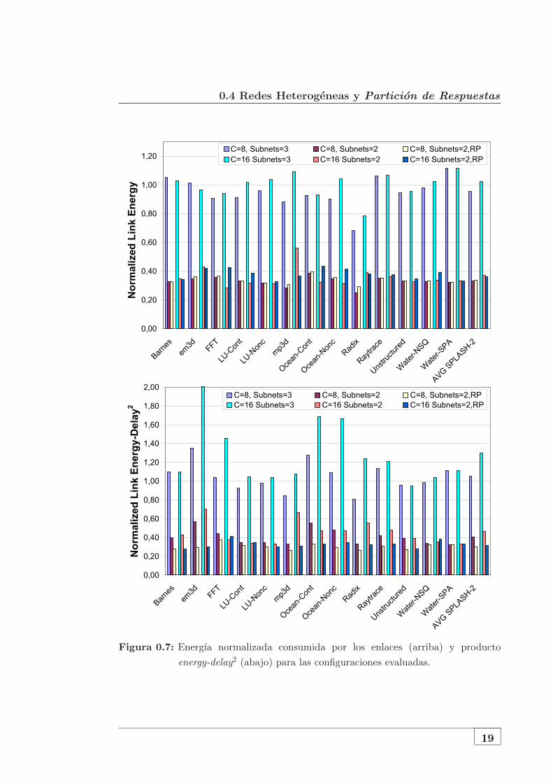
La Fig. 0.7 presenta las metricas de la energıa normalizada consumida en los
enlaces y el producto energy-delay2 (ED2P ). Nuestra propuesta muestra reduc-
ciones medias del 60%-65% en la energıa disipada por los enlaces internucleos.
18
0.4 Redes Heterogeneas y Particion de Respuestas
Figura 0.7: Energıa normalizada consumida por los enlaces (arriba) y producto
energy-delay2 (abajo) para las configuraciones evaluadas.
19
0. RESUMEN DE LA TESIS
Figura 0.8: Energıa normalizada y producto energy-delay2 para todo el CMP.
Esta reduccion es bastante similar para todas las aplicaciones. La metrica ED2P
tambien muestra buenos resultados con mejoras medias cercanas al 70% aunque,
en este caso, la variabilidad entre aplicaciones es mayor debido al mayor peso del
tiempo de ejecucion en la metrica ED2P .
Para finalizar, la Fig. 0.8 presenta las metricas de energıa normalizada y pro-
ducto ED2P para todo el CMP. Como se puede observar, nuestra propuesta
permite obtener importantes ahorros de consumo en todo el CMP. La magnitud
de estos ahorros depende del numero de nucleos, y van desde un 16% para la con-
figuracion de 8 nucleos a un 20% para la configuracion de 16 nucleos. Por otro
lado, cuando consideramos la metrica ED2P , las mejoras obtenidas van desde el
24% para el CMP de 8 nucleos al 30% para el de 16 nucleos, debido al mayor
peso del tiempo de ejecucion.
20

0.5 Redes Heterogeneas y Compresion de Direcciones
0.5 Redes Heterogeneas y Compresion de Direccio-
nes
Como se apunto anteriormente en la seccion 0.1, una manera de tratar los
problemas de retraso y consumo de los enlaces globales es el uso de redes hete-
rogeneas en las conexiones internucleo [4], es decir, una interconexion con enlaces
que estan compuestos de hilos con distintas propiedades de latencia y energıa [6].
Otra aproximacion para disminuir el consumo y los grandes retrasos asocia-
dos a los enlaces globales consiste en codificar la informacion transferida para
conseguir un mejor aprovechamiento del ancho de banda de la interconexion. El
espacio en area creado debido a la compresion se puede aprovechar para conseguir
mejoras adicionales en la latencia de los L-Wires. En esta seccion exploraremos
esta aproximacion proponiendo el uso de un esquema de compresion de direccio-
nes en el contexto de una interconexion heterogenea que permite que la mayor
parte de los mensajes crıticos usados en el mantenimiento de la coherencia sean
comprimidos en unos pocos bytes y transmitidos usando enlaces de muy baja
latencia (VL-Wires) mientras que el resto de mensajes se transmiten usando los
enlaces base (B-Wires). Es importante destacar que nuestro objetivo no es propo-
ner un esquema de compresion concreto sino explorar el uso del area que aparece
disponible cuando se usa la compresion para mejorar la latencia de los mensajes
crıticos mediante el uso de una interconexion heterogenea.
Como se discutio en la seccion 0.1.1.1, los L-Wires tienen un coste de area
cuatro veces superior al de los hilos base y, por tanto, el numero de L-Wires
esta bastante limitado. Considerando que seran utilizados para el envıo de men-
sajes cortos y crıticos, en la seccion anterior se fijo su numero de acuerdo con
el tamano tıpico de los mensajes cortos (es decir, 11 bytes). El resto de area se
utiliza para la implementacion de los enlaces utilizados para el envıo de los men-
sajes largos. Sin embargo, usando un esquema de compresion de direcciones la
cantidad de L-Wires puede reducirse drasticamente desde 11 bytes a 4-5 bytes
dependiendo del tamano de los bits de bajo orden no comprimidos usados por
el esquema de compresion subyacente. El espacio en area que aparece gracias a
la compresion puede entonces ser aprovechado para reducir aun mas la latencia
21
0. RESUMEN DE LA TESIS
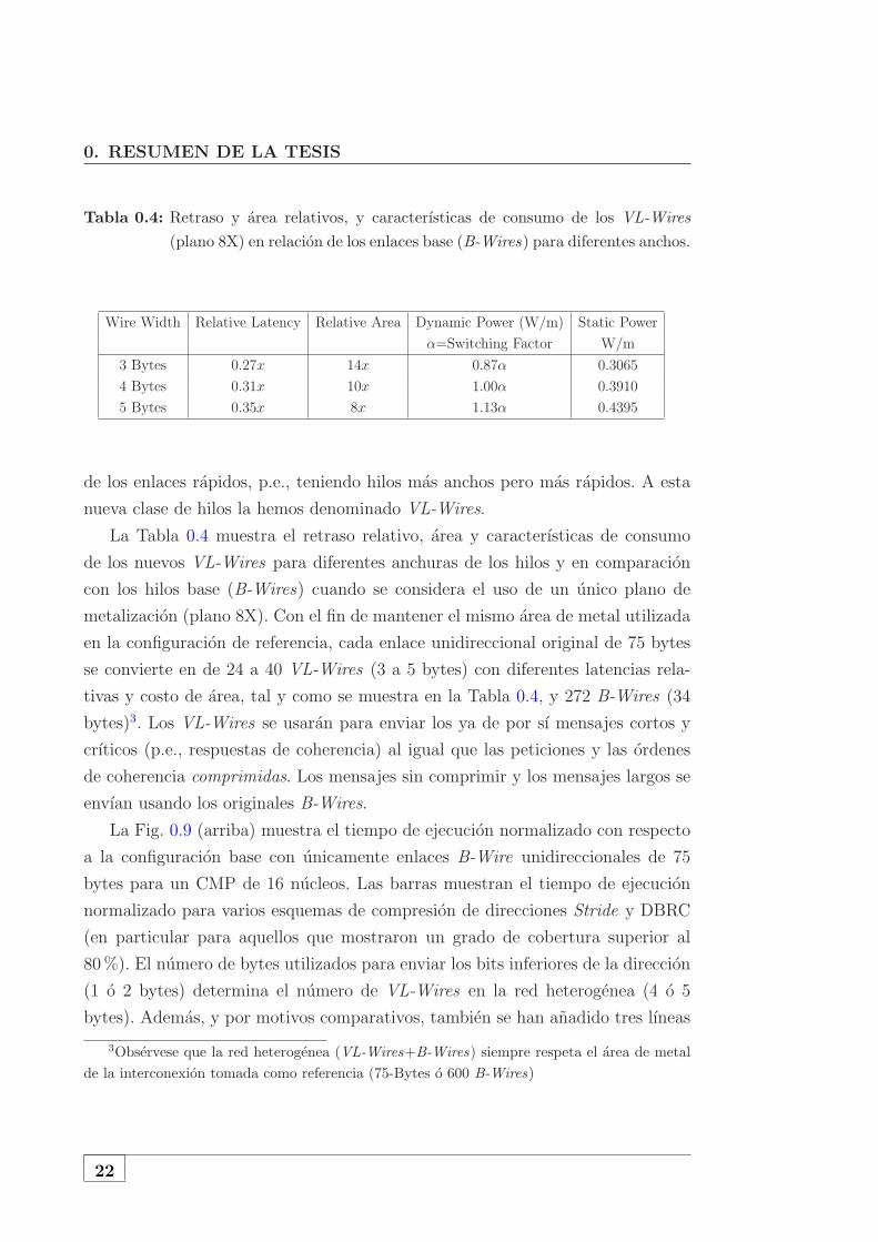
Tabla 0.4: Retraso y area relativos, y caracterısticas de consumo de los VL-Wires
(plano 8X) en relacion de los enlaces base (B-Wires) para diferentes anchos.
Wire Width Relative Latency Relative Area Dynamic Power (W/m) Static Power
α=Switching Factor W/m
3 Bytes 0.27x 14x 0.87α 0.3065
4 Bytes 0.31x 10x 1.00α 0.3910
5 Bytes 0.35x 8x 1.13α 0.4395
de los enlaces rapidos, p.e., teniendo hilos mas anchos pero mas rapidos. A esta
nueva clase de hilos la hemos denominado VL-Wires.
La Tabla 0.4 muestra el retraso relativo, area y caracterısticas de consumo
de los nuevos VL-Wires para diferentes anchuras de los hilos y en comparacion
con los hilos base (B-Wires) cuando se considera el uso de un unico plano de
metalizacion (plano 8X). Con el fin de mantener el mismo area de metal utilizada
en la configuracion de referencia, cada enlace unidireccional original de 75 bytes
se convierte en de 24 a 40 VL-Wires (3 a 5 bytes) con diferentes latencias rela-
tivas y costo de area, tal y como se muestra en la Tabla 0.4, y 272 B-Wires (34
bytes)3. Los VL-Wires se usaran para enviar los ya de por sı mensajes cortos y
crıticos (p.e., respuestas de coherencia) al igual que las peticiones y las ordenes
de coherencia comprimidas. Los mensajes sin comprimir y los mensajes largos se
envıan usando los originales B-Wires.
La Fig. 0.9 (arriba) muestra el tiempo de ejecucion normalizado con respecto
a la configuracion base con unicamente enlaces B-Wire unidireccionales de 75
bytes para un CMP de 16 nucleos. Las barras muestran el tiempo de ejecucion
normalizado para varios esquemas de compresion de direcciones Stride y DBRC
(en particular para aquellos que mostraron un grado de cobertura superior al
80%). El numero de bytes utilizados para enviar los bits inferiores de la direccion
(1 o 2 bytes) determina el numero de VL-Wires en la red heterogenea (4 o 5
bytes). Ademas, y por motivos comparativos, tambien se han anadido tres lıneas
3Observese que la red heterogenea (VL-Wires+B-Wires) siempre respeta el area de metal
de la interconexion tomada como referencia (75-Bytes o 600 B-Wires)
22

0.5 Redes Heterogeneas y Compresion de Direcciones
Figura 0.9: Tiempo de ejecucion normalizado (arriba) y metrica ED2P de los enla-
ces (abajo) para diferentes esquemas de compresion de direcciones sobre
enlaces heterogeneos (la anchura de los VL-Wires coincide con el tamano
de las direcciones comprimidas).
23

0. RESUMEN DE LA TESIS
solidas que muestran el tiempo de ejecucion para las diferentes configuraciones de
redes heterogeneas cuando se considera una cobertura de compresion perfecta4.
Se observa que un esquema de compresion DBRC de 4 entradas con dos bytes
de orden inferior es suficiente para conseguir una mejora media del rendimiento
del 8% (cerca del 10% del potencial maximo). Esta mejora presenta una alta
variabilidad, oscilando entre el 1-2% para Water y LU y el 22-25% para MP3D
y Unstructured. Esta variabilidad se debe a dos factores. En primer lugar,
algunas aplicaciones, como water o LU, presentan patrones de comparticion
de datos entre nucleos my escasos [96]. En estos casos, el trafico de coherencia
es pequeno y nuestra propuesta tiene poco impacto en el tiempo de ejecucion.
Otras aplicaciones, como MP3D o Unstructured, presentan mejores patrones
de trafico y pueden aprovechar una interconexion mas rapida. El segundo factor
que explica esta variabilidad esta relacionado con la cobertura del esquema de
compresion de direcciones. Aplicaciones como Barnes-Hut o Radix presentan
ratios bajos de compresion para la mayorıa de las configuraciones propuestas. Para
esas aplicaciones, la reduccion en el tiempo de ejecucion no alcanza el potencial
maximo incluso cuando se usa una configuracion con tablas de 64 entradas.
La Fig. 0.9 (abajo) muestra la metrica normalizada del producto energy-delay2
(ED2P ). Las mejoras medias estan cercanas al 40%, aunque de nuevo se observa
una gran variabilidad entre las aplicaciones. Algunas aplicaciones, comoWater y
LU, presentan reducciones de alrededor del 20% debido principalmente al menor
consumo de energıa de las redes heterogeneas; otras, como MP3D y Unstruc-
tured, muestran reducciones del 65% en la metrica ED2P debido al mayor peso
que el tiempo de ejecucion tiene en la metrica ED2P .
Por otro lado, la Fig. 0.10 muestra el tiempo de ejecucion normalizado (arriba)
y la metrica ED2P (abajo) cuando la anchura de los VL-Wires se restringe a 3
bytes, el tamano mınimo de los mensajes que circulan por la red, independiente-
mente del esquema de compresion usado. En este caso, los mensajes comprimidos
se envıan a traves de los VL-Wires usando fragmentacion. Esta configuracion
4Hablamos de cobertura de compresion perfecta cuando consideramos que el 100% de las
direcciones son comprimibles y que, por tanto, solo enviamos a traves de la red los bits inferiores
de las mismas.
24

0.5 Redes Heterogeneas y Compresion de Direcciones
Figura 0.10: Tiempo de ejecucion normalizado (arriba) y metrica ED2P de los enlaces
(abajo) para diferentes esquemas de compresion de direcciones sobre
enlaces heterogeneos VL-Wires de 3 bytes de anchura y fragmentacion
de los mensajes.
permite una latencia mınima para los mensaje de respuesta sin datos y las res-
25
0. RESUMEN DE LA TESIS
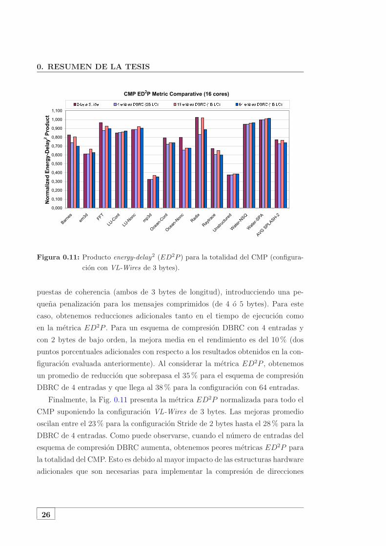
Figura 0.11: Producto energy-delay2 (ED2P ) para la totalidad del CMP (configura-
cion con VL-Wires de 3 bytes).
puestas de coherencia (ambos de 3 bytes de longitud), introducciendo una pe-
quena penalizacion para los mensajes comprimidos (de 4 o 5 bytes). Para este
caso, obtenemos reducciones adicionales tanto en el tiempo de ejecucion como
en la metrica ED2P . Para un esquema de compresion DBRC con 4 entradas y
con 2 bytes de bajo orden, la mejora media en el rendimiento es del 10% (dos
puntos porcentuales adicionales con respecto a los resultados obtenidos en la con-
figuracion evaluada anteriormente). Al considerar la metrica ED2P , obtenemos
un promedio de reduccion que sobrepasa el 35% para el esquema de compresion
DBRC de 4 entradas y que llega al 38% para la configuracion con 64 entradas.
Finalmente, la Fig. 0.11 presenta la metrica ED2P normalizada para todo el
CMP suponiendo la configuracion VL-Wires de 3 bytes. Las mejoras promedio
oscilan entre el 23% para la configuracion Stride de 2 bytes hasta el 28% para la
DBRC de 4 entradas. Como puede observarse, cuando el numero de entradas del
esquema de compresion DBRC aumenta, obtenemos peores metricas ED2P para
la totalidad del CMP. Esto es debido al mayor impacto de las estructuras hardware
adicionales que son necesarias para implementar la compresion de direcciones
26

0.6 Redes Heterogeneas y Prefetching Hardware EnergeticamenteEficiente
Figura 0.12: Tiempo de ejecucion normalizado y consumo de la red para un CMP de
16 nucleos para distintas tecnicas de prefetching.
y que no se ven compensadas por una reduccion significativa en el tiempo de
ejecucion.
0.6 Redes Heterogeneas y Prefetching Hardware Ener-
geticamente Eficiente
Como ya hemos ido comentando a lo largo de todo este resumen de la Tesis,
conforme el numero de nucleos dentro de un CMP aumente, la red de intercone-
xion on-chip tendra mayor impacto tanto en el rendimiento como en el consumo
global del CMP. En este contexto, los disenos CMP deberıan estar equipados
con tecnicas de ocultamiento de la latencia como la prebusqueda por hardware
(hardware prefetching) en un intento de reducir el impacto negativo sobre el ren-
dimiento que introducen las altas latencias que en estos sistemas presentaran los
fallos de cache. Desafortunadamente, el numero de mensajes extra que generan
los mecanismos tradicionales de prebusqueda puede aumentar de forma drastica
el consumo disipado por la interconexion de los futuros CMP compuestos por
decenas (e incluso centenas) de nucleos. Ası, en la Fig. 0.12 podemos observar las
mejoras en tiempo de ejecucion y el aumento de consumo en la red on-chip debido
27

0. RESUMEN DE LA TESIS
a las comunicaciones extra asociadas a esta tecnica para las tres alternativas de
prefetching hardware que se consideran a lo largo de esta seccion. Como se puede
observar, se obtienen aumentos de consumo superiores al 20% en la red on-chip
para algunas de estas tecnicas.
En esta seccion analizaremos como reducir el impacto de las tecnicas de
prebusqueda en terminos tanto de potencia disipada como de energıa consumi-
da en el contexto de tiled CMPs. Nuestra propuesta se basa en el uso de una
red heterogenea en donde los enlaces de bajo consumo se usan para el envıo de
los mensajes resultantes del prefetching, lo que nos permite conseguir mejoras de
hasta el 30% de la potencia consumida por la red (15-23% en promedio) con un
costo mınimo en terminos de tiempo de ejecucion (degradacion medıa del 2% con
respecto a un CMP de 16 nucleos que no incluya tal red heterogenea).
La Fig. 0.13 (arriba) muestra la fraccion de cada tipo de mensaje sobre el
numero total de mensajes para un CMP con 16 nucleos y considerando diferentes
mecanismos de prebusqueda. Los resultados estan normalizados con respecto a
una configuracion base sin ningun tipo de prebusqueda y solo hemos mostrado
aquellas aplicaciones en las cuales la prebusqueda supone una mejora significa-
tiva. Como se indico anteriormente, la utilizacion de mecanismos hardware de
prefetching incrementa de forma significativa la comunicacion dentro del chip,
obteniendose incrementos medios de alrededor del 20% en el trafico de la red. En
promedio, entre el 16% y el 34% del trafico que circula por la red esta relacio-
nado con la prebusqueda (peticiones de prefetch, las respuestas correspondientes
y todo el trafico de coherencia relacionado), mientras que el resto del trafico
esta relacionado con los mensajes ordinarios.
Mas interesante es la Fig. 0.13 (abajo) que muestra el desglose del consumo de
la red para cada tipo de mensaje. De nuevo, los resultados estan normalizados con
respecto al consumo de la red cuando no se utiliza ninguna tecnica de prefetching.
El porcentaje de consumo en la red asociado al trafico de prebusqueda oscila
entre el 17-18% cuando se utiliza el mecanismo mas complejo de prebusqueda
por stride, al 32-40% para los esquemas mas simples.
La Fig. 0.14 muestra el tiempo de ejecucion normalizado con respecto al ob-
tenido en la configuracion base para un CMP de 16 nucleos sin prebusqueda.
Las barras muestran el tiempo de ejecucion para las tecnicas prefetch-on-miss
28

0.6 Redes Heterogeneas y Prefetching Hardware EnergeticamenteEficiente
Figura 0.13: Desglose de los mensajes que circulan a traves de la red de interconexion
para un CMP de 16 nucleos (arriba) y porcentaje de consumo en la
red por cada tipo de mensaje (abajo) cuando se consideran diferentes
mecanismos de prefetching.
29

0. RESUMEN DE LA TESIS
Figura 0.14: Tiempo de ejecucion normalizado para diferentes esquemas de
prebusqueda (con y sin enlaces heterogeneos) para un CMP de 16
nucleos.
30

0.6 Redes Heterogeneas y Prefetching Hardware EnergeticamenteEficiente
Figura 0.15: Clasificacion de los diferentes tipos de prebusquedas observadas para la
interconexion original (arriba) y heterogenea (abajo).
31

0. RESUMEN DE LA TESIS
(OnMiss), tagged prefetch (Tagged) y stride-based prefetch (Stride) aplicadas la
cache L1 de datos. Por razones comparativas, tambien se muestra el tiempo de
ejecucion normalizado cuando se utiliza una red no heterogenea. En promedio, se
obtienen mejoras en el tiempo de ejecucion de alrededor del 10% para todas las
tecnicas de prebusqueda evaluadas, lo que demuestra la conveniencia del uso de la
prebusqueda en los futuros tiled CMPs. Estas mejoras presentan una alta varia-
bilidad, oscilando entre casi imperceptibles o incluso una ligera degradacion para
Barnes-Hut, Raytrace, Unstructured y Water a mejoras del 20-35%
para EM3D y Ocean-Cont.
Esta variabilidad se debe al patron de acceso a memoria que muestran las
diferentes aplicaciones. Algunas aplicaciones, como FFT, LU-Cont o Ocean-
Cont presentan patrones regulares de acceso a memoria lo que da lugar a un
alto porcentage de prebusquedas utiles tal y como podemos apreciar en la Fig.
0.15 (arriba) en donde presentamos una clasificacion de las prebusquedas. En esta
figura, las prebusquedas se clasifican en: useful si se accede a la lınea prebuscada
antes de ser reemplazada, late si aparecen otras peticiones sobre la lınea que hemos
solicitado, useless si la lınea prebuscada es reemplazada antes de ser utilizada
por el procesador, unnecesary si la prebusqueda se realiza sobre una lınea que
ya ha sido solicitada debido a un fallo de cache anterior e invalidated si la lınea
prebuscada es invalidada antes de ser solicitada por el procesador. Por otro lado,
aplicaciones como Barnes-Hut o Raytrace muestran un alto porcentaje de
prebusquedas tardıas o inutiles lo que da lugar a mejoras marginales en el tiempo
de ejecucion
Volviendo a la Fig. 0.14, cuando consideramos enlaces heterogeneos, se obtie-
ne una degradacion del orden del 2% en relacion con la configuracion que usa
unicamente enlaces B-Wire y prefetching. En este caso se observa degradaciones
similares para todas las aplicaciones en estudio. Esta degradacion se explica por
el retraso adicional en el que se incurre cuando se envıan los mensajes con las
lıneas prebuscadas haciendo uso de los enlaces PW-Wires. La Fig. 0.15 (abajo)
muestra que el 5% de lo que antes eran prebusquedas utiles se tornan en tardıas,
lo que explica el enlentecimiento observado.
Sin embargo, los beneficios del uso de una red heterogenea en el contexto
del prefetching, tal y como proponemos, puede observarse cuando se considera el
32

0.6 Redes Heterogeneas y Prefetching Hardware EnergeticamenteEficiente
Figura 0.16: Consumo normalizado de los enlaces para diferentes esquemas de prefet-
ching sobre enlaces heterogeneos (configuracion base: CMP de 16 nucleos
con prefetching).
consumo de la red. La Fig. 0.16 muestra el consumo normalizado de los enlaces
cuando los mensajes que llevan las lıneas prebuscadas son enviados a traves de
enlaces PW-Wires. Se puede observar reducciones de hasta el 30% (15-23% en
promedio), con una menor variabilidad entre las aplicaciones. Los mejores resul-
tados se obtienen, tal y como cabıa esperar, para las tecnicas de prebusqueda
OnMiss y Tagged debido a que estas tecnicas son las que generan mas trafico
relacionado con el prefetching (como se vio en la Fig. 0.13). Lo que genera reduc-
ciones mas importantes en el consumo de los enlaces cuando las lıneas prebus-
cadas son enviadas a traves de los enlaces PW-Wires. Estas mejoras se traducen
en reducciones de hasta el 10% en la energıa total consumida por el CMP para
aplicaciones como EM3D o Ocean-Cont, con una reduccion media del 4% (ver
Fig. 0.17).
33

0. RESUMEN DE LA TESIS
Figura 0.17: Normalizacion de la energıa disipada por la totalidad del CMP.
0.7 Conclusiones y Vıas Futuras
En los ultimos anos hemos asistido a la evolucion de la arquitectura de los
microprocesadores desde disenos monolıticos a la integracion de multiples nucleos
de procesamiento en un unico chip. Hoy en dıa, las arquitecturas multinucleo se
vislumbran como la unica manera de asegurar mejoras en el rendimiento. De
esta manera, la mayor parte de la industria esta de acuerdo en afirmar que el
diseno multinucleo es el camino a elegir y que en esta decada llegaremos a tener
disenos con decenas de nucleos. En este contexto la comunicacion surge como una
limitacion cada vez mayor tanto desde el punto de vista del consumo como del
rendimiento, siendo necesario buscar nuevas aproximaciones para manejar el alto
coste de la comunicacion dentro del chip a traves de los enlaces globales en estas
arquitecturas tiled CMP.
Los esfuerzos en esta Tesis se han centrado en explotar las propiedades de los
enlaces de la red de interconexion con el fin de encontrar formas de aliviar el cuello
de botella que la comunicacion dentro del propio chip supone a la hora de obtener
34

0.7 Conclusiones y Vıas Futuras
un alto rendimiento y un consumo eficiente en el contexto de arquitecturas tiled
CMP. De esta manera se han propuesto y evaluado tecnicas encaminadas a reducir
la latencia de los enlaces globales y la disipacion de potencia de la interconexion
on-chip en arquitecturas CMP. Para la correcta evaluacion de estas tecnicas fue
necesario disenar y posteriormente implementar Sim-PowerCMP, un simulador
a nivel de arquitectura basado en RSIM x86 que permite la estimacion tanto
del consumo estatico como dinamico para arquitecturas CMP. A partir de las
evaluaciones realizadas sobre Sim-PowerCMP se pueden extraer una serie de
conclusiones importantes.
La primera conclusion que podemos resaltar es que la correcta organizacion
de la red de interconexion a la vez que el manejo adecuado de los diferentes
tipos de mensajes que circulan a traves de ella tienen un impacto significativo
en la energıa consumida por los CMPs; especialmente en el caso de la siguiente
generacion de arquitecturas CMP densas. Reply Partitioning (ver capıtulo 3 de
esta Tesis) se aprovecha de esta conclusion a traves de la division de los mensajes
de respuesta con datos en un mensaje corto crıtico que contiene el subbloque de
la cache solicitado por el nucleo y un mensaje largo no crıtico con el contenido
completo de la lınea de cache. Nuestra propuesta esta motivada por la observacion
de que cuando el procesador solicita un dato que no se encuentra en la cache L1
(fallo de cache L1), la totalidad de la lınea puede no ser necesaria en ese momento,
siendo suficiente con un pequeno subconjunto de la misma. De esta manera,
dividiendo las respuestas con datos en Partial Replies y Ordinary Replies, todos
los mensajes crıticos pasan a ser cortos (observese que los mensajes Partial Replies
son crıticos ya que contienen la palabra solicitada por el procesador) y, por tanto,
pueden ser enviados usando los enlaces de baja latencia constituidos a partir
de L-Wires. Al mismo tiempo, todos los mensajes largos son ahora no crıticos
(observese que los mensajes Ordinary Replies son no crıticos ya que la palabra
solicitada ya viaja en un mensaje corto que con alta probabilidad llegara antes
a su destino) y, por tanto, pueden enviarse usando enlaces constituidos por PW-
Wires (de bajo consumo) sin danar al rendimiento. Los resultados obtenidos a
traves de simulaciones muestran que nuestra propuesta puede reducir en un 65%
el consumo de los enlaces con una reduccion adicional del 7% en el tiempo de
ejecucion. Finalmente, estas reducciones se trasladan en reducciones de energıa
35

0. RESUMEN DE LA TESIS
para el CMP en su totalidad que van desde el 16% para la configuracion de 8
nucleos hasta el 20% para la de 16 nucleos (del 24% al 30% si se considera la
metrica ED2P ).
Otra aproximacion para aliviar los problemas anteriormente mencionados es
transcodificar la informacion transferida de manera que se explote mejor el ancho
de banda de la interconexion. Mediante tecnicas de compresion de informacion, el
area sobrante de los enlaces no usados puede explotarse para mejorar aun mas la
latencia de determinados enlaces. De esta manera, la latencia total del directorio
puede reducirse en aquellos casos en donde algunos de los mensajes utilizan estos
enlaces de muy baja latencia. Esto reduce el tiempo necesario para satisfacer un
fallo de cache L2 y constituye el punto de partida del capıtulo 4.
Dicho capıtulo propone el uso de un esquema de compresion de direcciones en
el contexto de una red de interconexion heterogenea que permite que la mayorıa
de los mensajes crıticos, usados para mantener la coherencia entre las caches L1
de un CMP, sean comprimidos en unos pocos bytes y transmitidos usando enlaces
de muy baja latencia, mientras que el resto de los mensajes siguen usando enlaces
base. El capıtulo comienza analizando la efectividad de diferentes esquemas de
compresion de direcciones en el contexto de un tiled CMP que ejecuta aplicacio-
nes paralelas. Posteriormente se estiman las caracterısticas de area y consumo de
diferentes configuraciones de los esquemas de compresion utilizando CACTI v4.1
y suponiendo un proceso de fabricacion de 65 nm. Finalmente, proponemos un
nuevo diseno de interconexion basado en el uso de un esquema de compresion de
direcciones que permite reducir drasticamente la cantidad de L-Wires necesarios,
de 11 bytes a 4-5 bytes en funcion del tamano de los bits de orden inferior usa-
dos por el esquema de compresion subyacente. El area sobrante se utiliza para
mejorar la latencia de los enlaces rapidos haciendolos mas anchos (VL-Wires).
Los resultados obtenidos muestran que esta propuesta de manejo de mensajes on-
chip puede reducir la metrica ED2P para los enlaces de la red de interconexion
en torno al 38% con una reduccion adicional en el tiempo de ejecucion del 10%.
Estas reducciones se traducen en mejoras del 28% para todo el CMP cuando se
considera la metrica ED2P .
Otra manera de manejar los problemas debidos a las altas latencias de los
enlaces globales es el uso de tecnicas de ocultamiento de la latencia como el pre-
36

0.7 Conclusiones y Vıas Futuras
fetching por hardware. Desafortunadamente, el numero de mensajes extra que
generan los mecanismos de prebusqueda (prefetching) tradicionales puede au-
mentar de forma drastica el consumo disipado por la interconexion de los futuros
CMP compuestos por decenas (e incluso centenas) de nucleos. El uso de una
red heterogenea en este contexto nos permite mejorar la eficiencia energetica de
las tecnicas de prebusqueda mediante la transmision de las lıneas prebuscadas a
traves de enlaces de bajo consumo mientras que el resto de los mensajes se con-
tinuan transmitiendo usando enlaces de base. Esta propuesta constituye la base
de la investigacion presentada en el capıtulo 5. Los resultados obtenidos a traves
de simulaciones para un CMP de 16 nucleos muestran que nuestra propuesta
puede reducir el consumo de los enlaces de la red de interconexion alrededor del
23% con una degradacion del 2% en el tiempo de ejecucion. Estas reducciones
se traducen en mejoras de hasta el 10% (4% en promedio) cuando se considera
la energıa consumida por la totalidad del CMP.
En resumen, en esta Tesis hemos presentado distintas tecnicas orientadas a
reducir los altos costes, en terminos de latencia y disipacion de potencia, que
introduce la interconexion on-chip de los futuros tiled CMP densos. Hemos visto
como el uso de enlaces heterogeneos puede reducir el consumo de la red on-chip sin
afectar al rendimiento. Al mismo tiempo, este tipo de enlaces nos permite realizar
implementaciones que aceleran de forma significativa los fallos de cache al reducir
el tiempo necesario para que cierto tipo de mensajes crıticos viajen a traves
de la interconexion y por tanto minimizar los efectos negativos causados por la
indireccion introducida por el uso de directorios. Ademas, hemos mostrado como
la compresion de direcciones puede ser aplicada en muchos casos para reducir
todavıa mas la latencia del camino crıtico de los fallos de cache.
Los resultados presentados en esta Tesis abren una serie de caminos intere-
santes en la investigacion. Entre ellos, podemos identificar los siguientes:
Deseamos explorar la aplicacion de nuestras propuestas sobre nuevas pro-
puestas de protocolos de coherencia de caches [65; 76]. Esperamos que, en
la mayorıa de los casos, las mismas tecnicas puedan ser aplicadas facilmente
a un amplio rango de protocolos con algunas pequenas modificaciones.
37

0. RESUMEN DE LA TESIS
Creemos que usando esquemas de prebusqueda mas avanzados como el loo-
kahead program counter (LA-PC) stride prefeching [16], que es similar al
stride prefetching basico pero controlado por el LA-PC, podremos reducir
la pequena degradacion en el tiempo de ejecucion que nuestra propuesta de
uso conjunto de la prebusqueda con una red heterogenea experimenta.
Tambien deseamos explorar las interacciones existentes entre nuestras pro-
puestas: Particion de Respuestas, compresion de direcciones y prebusqueda
hardware. Los primeros resultados muestran que las mismas interactuan
de manera negativa debido a que cada tecnica esta ligada a una red he-
terogenea especıficamente disenada para esa tecnica, pero creemos que es
posible disenar una red que satisfaga los requisitos de varias de las tecnicas
propuestas.
Finalmente, otra vıa de investigacion prometedora es el uso de la compresion
de datos a traves de valores/patrones frecuentes. Creemos que la compre-
sion de datos puede interactuar positivamente con nuestras propuestas de
Particion de Respuestas y/o prebusqueda hardware.
38

1Introduction
1.1 Motivation and Foundations
Integration capacity of billions of transistors exists today, and will double
every two years for the next decade. This trend is shown in Fig. 1.1 (green
line), starting from 1971 to the present day. Asumming about half of the die
area being allocated for logic, and the other half for large memory arrays such
as caches, by 2015 it will be possible to integrate 100B transistors on a 300mm2
die, with almost 1.5B transistors1 available for logic [12].
As implementation technology scales down, high performance processor de-
signs have evolved from monolithic designs toward architectures that integrate
multiple processing cores on a single die. Large uniprocessors are no longer scal-
ing in performance because it is only possible to extract a limited amount of
parallelism from a typical instruction stream using conventional superscalar in-
struction issue techniques. In addition, one cannot simply increase the clock
speed on today’s processors, or the power dissipation would become prohibitive
in all but water-cooled systems. Compounding these problems is the simple fact
that with the immense number of transistors available on today’s microprocessor
chips, it is too costly to design and debug ever-larger processors every year or
two.
This ability to integrate more and more transistors on a single chip has also
been, albeit indirectly, responsible for some of the most important changes that,
1The logic transistors tend to be larger than transistors in the memory, take larger space,
and consume more power.
39

1. INTRODUCTION
Figure 1.1: Evolution of the transistor integration capacity, power consumption, clock
frequency, and instruction-level parallelism (ILP) (source: D. Patterson,
UC–Berkeley).
from the architectural point of view, we have experienced in the design of micro-
processors in recent decades: the emergence of architectures that implement mul-
tiple processing cores on a single die, commonly known as chip-multiprocessors
or multicore architectures.
Indeed, in the last years we have witnessed the evolution from monolithic
designs to architectures that integrate multiple processing cores on a single chip.
Fig. 1.1 also shows the factors underlying this evolution in processor design. As
it can be seen, since about ten years it became evident that large monolithic
designs were unable to extract enough parallelism of typical instruction stream
of a program by using conventional superscalar instruction issue techniques (note
how the violet line, which represents the performance per clock cycle, stabilizes
40

1.1 Motivation and Foundations
around 2003). The alternative to further increase the operating frequency of the
microprocessor was only possible during three/four more years, after which it be-
came clear that it was impossible to keep increasing the clock frequency without
using expensive cooling systems because of the increased power dissipation de-
rived from higher clock rates. Adding the simple fact that with the huge number
of transistors available on today’s chips is too expensive to design and debug a
new monolithic processor every one or two years, we have all the factors that
explain the evolution from monolithic designs to multi-core architectures, also
known as CMPs (Chip Multiprocessors).
Chip Multiprocessors avoid these problems by filling up a processor die with
multiple, relatively simpler processor cores instead of just one huge core. Today,
multi-core architectures are envisioned as the only way to ensure performance
improvements. In this way, most of the industry would agree that multi-core is the
way forward and that designs with tens of cores on the die will be a reality within
this decade. As an example, Intel recently unveiled an 80-core research prototype
called Polaris [91] and Tilera Company launched this year its TILE64 processor
that implements a 64-core architecture connected through five bi-dimensional
meshes, each of which specializes in a different use [95]. Additionally, future
many-core CMPs with several tens (or even hundreds) of processor cores probably
will be designed as arrays of replicated tiles connected over an on-chip switched
direct network [88; 98]. These tiled architectures have been claimed to provide
a scalable solution for managing the design complexity, and effectively using the
resources available in advanced VLSI technologies. Maybe, one of the best known
examples of a tiled CMP architecture today is the already mentioned 80-core
Intel’s Polaris prototype [91].
Therefore, envisioning a future where we will have tens (or hundreds) of pro-
cessing cores, it is necessary to provide a programming model easy to understand
by programmers and flexible enough to efficiently implement other programming
models on top of it. During many years the shared memory model, where the no-
tion of a single main memory which is accessed by all the cores and through which
the communication between them is implicitly made, has proven to possess the
qualities described above and, we believe it is safe to assume that it will remain
the dominant programming model for a long time. Even if better programming
41

1. INTRODUCTION
models emerge in the future, shared memory will still need to be efficiently sup-
ported, at least, due to the sheer quantity of software already developed using
it.
The need to efficiently implement a shared memory programming model has
a direct influence on the design of tiled CMP architectures. Specifically, these
architectures must implement a cache coherency subsystem in order to preserve
the notion of a global address memory space in the presence of private caches
that allow the existence of multiple copies of a particular memory line that could
lead to inconsistencies on the memory contents.
Cache coherence ensures that writes to shared memory are eventually made
visible to all processors and that writes to the same location appear to be seen in
the same order by all processors [34] even in presence of caches. Cache coherence is
enforced by means of cache coherence protocols [21] which arbitrate the exchange
of data and access permissions between processors, caches and memories.
There are a number of coherence protocols available to enforce coherence.
Deciding the best coherence protocol for a system depends on the characteristics
of the system. There are three main approaches to designing a cache coherence
protocol:
Snooping-based protocols [35]: All requests are broadcast to all coher-
ence nodes using an interconnect which guarantees total order2 of messages,
like a shared bus. The total order property of the interconnect is used to
serialize potentially conflicting requests, since all nodes snoop the bus and
see all the requests in the same order.
Directory-based protocols [14]: Requests are sent to a single node
(which may be different for different addresses) which forwards it to all
the nodes that need to be involved because they have data and they need
to invalidate it or send it to the requestor. That single node has all the
information about the current sharers of the data in a directory and serves
as the serialization point for requests to the same address. Directory-based
2Total order of messages means that messages are received by all destinations in the same
order that they are sent, keeping the relative order even for messages which are sent to different
destinations or from different sources.
42

1.1 Motivation and Foundations
(a) Block diagram of an in-
dividual tile.
(b) 16-core CMP with a 2D-
mesh interconnection net-
work.
Figure 1.2: Tiled CMP architecture considered along this Thesis.
protocols do not need a totally ordered network and are appropriate for
point-to-point interconnects3 but the extra indirection introduced by the
directory increases the latency of cache misses.
Token-based protocols [63]: Token coherence provides a way to avoid
the indirection introduced by directory-based protocols while using an in-
terconnect which does not provide total order of requests. Most requests
in a token coherence protocol are not serialized by any means. Instead,
coherence is ensured by a set of token counting rules. Token counting rules
are enough to ensure that coherence is kept but they are not enough to
ensure that requests are actually satisfied. For ensuring this, token-based
cache coherence protocols need to provide additional mechanisms that en-
sure forward progress even in presence of request races. Currently proposed
token-based protocols ensure forward progress by means of persistent re-
quests when races are detected. These persistent requests are serialized by
a centralized or distributed arbiter.
3Although point-to-point interconnects do not guarantee total order of messages, they may
guarantee point-to-point order of messages. That is, two messages are delivered in the same
relative order as they are sent as long as both have the same source and destination. Many
point-to-point interconnects provide point-to-point ordering guarantees, but not all.
43

1. INTRODUCTION
Of all the approaches seen above, only directory-based and token-based pro-
tocols are suitable for a tiled CMP architecture as they can be used in the context
of a point-to-point on-chip interconnection network. In this Thesis we consider
a tiled CMP architecture with support for cache coherence using a directory-
based approach as shown in Fig. 1.2. In this architecture, each tile contains
a processing core with first-level private caches (both instruction and data), a
portion of the L2 cache and a connection to the on-chip network. The L2 cache
is shared among multiple cores and it is physically distributed among them. In
addition, the L2 cache stores (in the tags’ part of the local L2 slice) the directory
information needed to ensure coherence between the L1 caches. On a L1 cache
miss, a request is sent down to the appropriate tile where further protocol actions
are initiated based on that block’s directory state, such as invalidation messages,
intervention messages, data writebacks, data block transfers, etc. We assume a
process technology of 65 nm, a tile area of approximately 25 mm2, and a die size
in the order of 400 mm2 [98; 100]. Note that this area is similar to the largest die
in production today (Itanium 2 processor – around 432 mm2 [58]). Note also that
due to manufacturing costs and form factor limitations, it would be desirable to
keep die size as low as possible [100].
1.1.1. The Global Communication Problem in Tiled CMP
Architectures
One of the greatest bottlenecks to high performance and energy efficiency in
such tiled CMP architectures is the high cost of on-chip communication through
global wires [40]. Wang et al. [93] reported that the on-chip network of the Raw
processor [88] consumes 36% of the total chip power. Magen et al. [62] also
attribute 50% of overall chip power to the interconnect. Most of this power is
dissipated in the point-to-point links of the interconnect [93]. Thus, wires pose
major performance and power dissipation problems as technology shrinks and
total die area increases. This trend will be exacerbated in future many-core CMP
designs. Therefore, as communication emerges as a larger power and performance
constraint than computation itself, wire properties should be exposed to architects
in order to enable them to find ways to exploit these properties.
44

1.1 Motivation and Foundations
Rgate/ W Cdiff* W * a Cgate* W * a
Rwire* l * lCwire
Figure 1.3: First-order repeater model.
1.1.1.1. Wire Implementation in Heterogeneous Networks
The delay of a wire can be modeled as a first-order RC circuit [40] (see Fig.
1.3). In that model, a CMOS driver is seen as a simple resistor, Rgate, with a
parasitic load, Cdiff , as shown in Equation 1.1. The CMOS receiver at the other
end of the wire presents a capacitive load Cgate. Cwire and Rwire are the wire
resistance and capacitance, respectively. Other parameters of importance are the
transistor width w, the wire length l, and the normalized sum of NMOS+PMOS
gate widths a.
Delay ∝ Rgate(Cdiff + Cwire + Cgate) +Rwire(1
2Cwire + Cgate)
�
�
�
�1.1
The resistance per unit length of the wire, Rwire, depends on the geometrical
dimensions of the wire cross-section. Increasing the width of the wire can signif-
icantly decrease its resistance although a modest increase in Cwire is produced.
Similarly, increasing the spacing between adjacent wires results in a Cwire drop.
Combining both factors allows for wire designs with lower delays.
Furthermore, the delay of an uninterrupted wire grows quadratically with its
length. Therefore, for long wires, designers must insert repeaters periodically
along the wire to break this quadratic dependence of wire delay on the wire
length. As repeaters divide a long wire into multiple shorter segments of length
l, the total wire delay is the number of segments times the individual segment
delay. Each segment’s delay is still quadratically dependent on its segment length,
but the total wire delay is now linear with total length. Overall wire delay can
be minimized by selecting optimal repeater sizes and spacing between repeaters,
being a commonly employed technique nowadays.
45
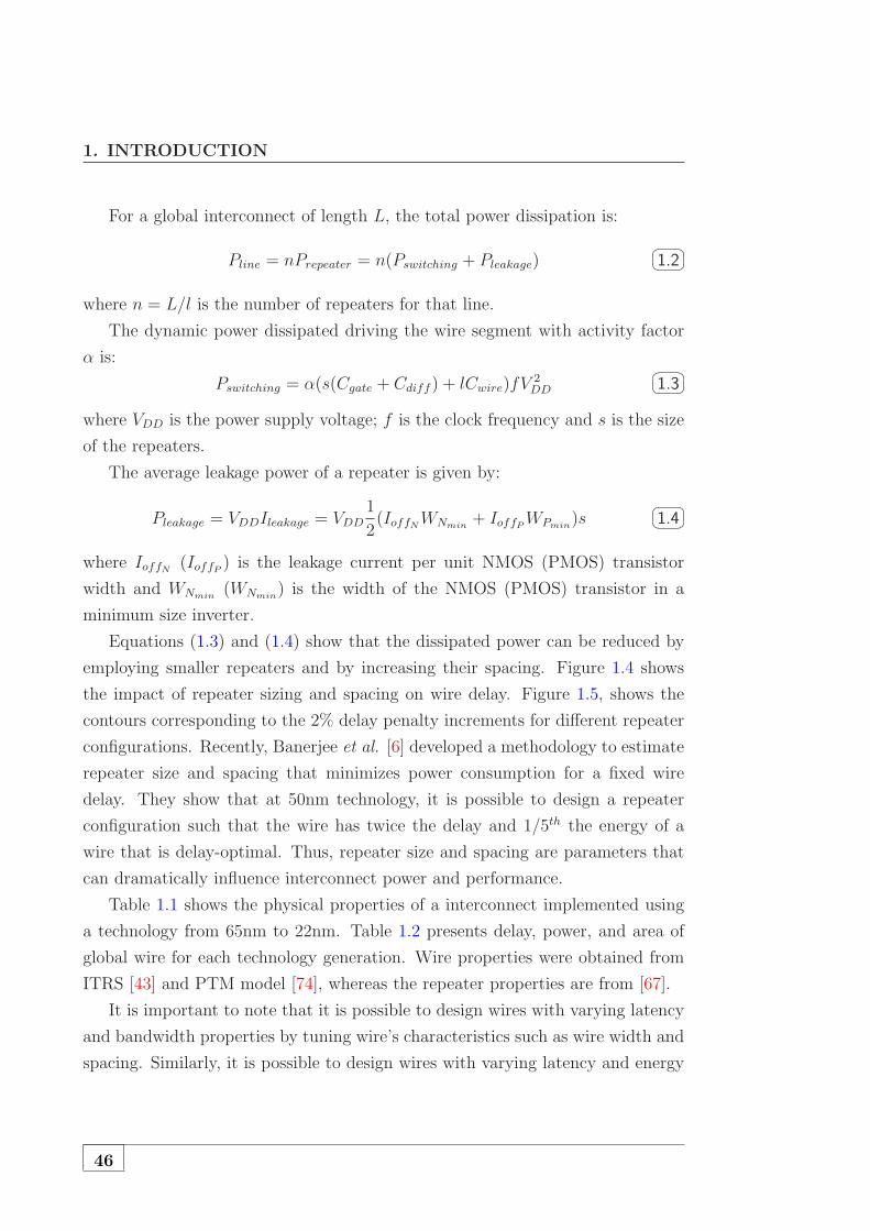
1. INTRODUCTION
For a global interconnect of length L, the total power dissipation is:
Pline = nPrepeater = n(Pswitching + Pleakage)�
�
�
�1.2
where n = L/l is the number of repeaters for that line.
The dynamic power dissipated driving the wire segment with activity factor
α is:
Pswitching = α(s(Cgate + Cdiff ) + lCwire)fV2
DD
�
�
�
�1.3
where VDD is the power supply voltage; f is the clock frequency and s is the size
of the repeaters.
The average leakage power of a repeater is given by:
Pleakage = VDDIleakage = VDD
1
2(IoffNWNmin
+ IoffPWPmin)s
�
�
�
�1.4
where IoffN (IoffP ) is the leakage current per unit NMOS (PMOS) transistor
width and WNmin(WNmin
) is the width of the NMOS (PMOS) transistor in a
minimum size inverter.
Equations (1.3) and (1.4) show that the dissipated power can be reduced by
employing smaller repeaters and by increasing their spacing. Figure 1.4 shows
the impact of repeater sizing and spacing on wire delay. Figure 1.5, shows the
contours corresponding to the 2% delay penalty increments for different repeater
configurations. Recently, Banerjee et al. [6] developed a methodology to estimate
repeater size and spacing that minimizes power consumption for a fixed wire
delay. They show that at 50nm technology, it is possible to design a repeater
configuration such that the wire has twice the delay and 1/5th the energy of a
wire that is delay-optimal. Thus, repeater size and spacing are parameters that
can dramatically influence interconnect power and performance.
Table 1.1 shows the physical properties of a interconnect implemented using
a technology from 65nm to 22nm. Table 1.2 presents delay, power, and area of
global wire for each technology generation. Wire properties were obtained from
ITRS [43] and PTM model [74], whereas the repeater properties are from [67].
It is important to note that it is possible to design wires with varying latency
and bandwidth properties by tuning wire’s characteristics such as wire width and
spacing. Similarly, it is possible to design wires with varying latency and energy
46

1.1 Motivation and Foundations
Figure 1.4: Effect of repeater spacing/sizing on wire delay (source: [70]).
Figure 1.5: Contours for 2% delay penalty (source: [70]).
47

1. INTRODUCTION
Table 1.1: Global interconnect evolution and characteristics (source: [45]).
Year 2007 2010 2013 2016
Technology 65nm 45nm 32nm 22nm
supply voltage, Vdd (V) 1.1 1.0 0.9 0.8
clock freq. (GHz) 6.73 11.51 19.3 28.8
pitch (nm) 210 135 96 66
aspect ratio 2.3 2.4 2.5 2.6
width (nm) 105 68 48 33
spacing (nm) 105 68 48 33
thickness (nm) 241.5 163.2 120 85.8
height(ILD) (nm) 241.5 163.2 120 85.8
dielectric permittivity 2.85 2.65 2.25 2.15
Rw (Ohm/mm) 867.593 1982.41 3819.444 7770.007
cs (fF/mm) 21.955 19.569 15.948 14.647
ci (fF/mm) 81.354 79.297 70.425 70.251
cw = 2cs + 2ci (fF/mm) 206.618 197.732 172.746 169.796
Table 1.2: Global interconnect delay/power (source: [45]).
Year 2007 2010 2013 2016
Technology 65nm 45nm 32nm 22nm
hopt (mm) 0.491 0.318 0.268 0.190
47.113 38.248 36.794 36.536
kopt one segment wire delay (ps) 59.175 58.086 66.528 66.528
unit length delay (ps/mm) 20.542 182.750 247.896 350.543
unit length delay (FO4/mm) 5.151 11.281 21.519 44.260
unit length dynamic power (mW/mm) 2.045 1.513 1.119 0.869
unit length leakage power (uW/mm) 1.441 1.625 1.777 2.338
unit length sc power (mW/mm) 0.331 0.257 0.214 0.184
unit length total power (mW/mm) 2.378 1.771 1.336 1.056
48

1.1 Motivation and Foundations
Table 1.3: Area, delay, and power characteristics of wire implementations (source:
[17]).
Wire Type Relative Relative Dynamic Power (W/m) Static Power
Latency Area α=Switching Factor W/m
B-Wire (8X plane) 1x 1x 2.65α 1.0246
B-Wire (4X plane) 1.6x 0.5x 2.9α 1.1578
L-Wire (8X plane) 0.5x 4x 1.46α 0.5670
PW-Wire (4X plane) 3.2x 0.5x 0.87α 0.3074
properties by tuning repeater size and spacing [6]. Therefore, using links that
are comprised of wires with different physical properties, a heterogeneous on-chip
interconnection network is obtained.
In the case of a tiled CMP architecture with cache coherence, there exist a
variety of coherence operations with different bandwidth and latency needs4. Be-
cause of this diversity, there are many opportunities to improve performance and
power characteristics by employing a heterogeneous interconnect. For example,
in a directory-based protocol, on a cache write miss, the requesting processor
may have to wait for data from the home node (a two hop transaction) and for
acknowledgments from other sharers of the block (a three hop transaction). Since
the acknowledgments are on the critical path and have low bandwidth needs, they
can be mapped to wires optimized for delay, while the data block transfer is not
on the critical path and can be mapped to wires that are optimized for low power.
Cheng et al. [17] proposed to develop a heterogeneous interconnect comprised
of two wire implementations apart from baseline wires (B-Wires): power opti-
mized wires (PW-Wires) that have fewer and smaller repeaters, and bandwidth
optimized wires (L-Wires) with bigger widths and spacing. Then, coherence
messages are mapped to the appropriate set of wires taking into account, among
others, their latency and bandwidth requirements.
Table 1.3 shows the relative delay, area, and power characteristics of L- and
PW-Wires compared to baseline wires (B-Wires), as reported in [17]. A 65 nm
4Note that if we consider that inter-core communication is done using message passing, mes-
sages size and criticality cannot be obtained easily and the use of a heterogeneous interconnect
would make nosense.
49

1. INTRODUCTION
process technology is considered assuming ten metal layers: four layers in the 1X
plane, and two layers in each 2X, 4X, and 8X planes [55]. 4X and 8X metal planes
are used for global inter-core wires. It can be seen that L-Wires yield a two-fold
latency improvement at a four-fold area cost. On the other hand, PW-Wires are
designed to reduce power consumption with twice the delay of baseline wires (and
the same area cost). As in [55], it is assumed that 4X and 8X wires are routed
over memory arrays.
1.1.2. Router Implementation in Heterogeneous Networks
Fig. 1.6 illustrates the architecture of a generic 5-port, 2-stage NoC router
employing virtual channel flow control and wormhole switching. The five ports
correspond to the four cardinal directions and the connection to the local Pro-
cessing Element (PE). The router consists of six major components: the Routing
Computation unit (RC), the Virtual Channel Allocator (VA), the Switch Allo-
cator (SA), the MUXes and DEMUXes which control the flit flow through the
router, the VC buffers, and the crossbar. A flit is the smallest unit of flow control
and is usually the number of bits transmitted on a link in a single cycle. The
size of the message sent through the network is measured in terms of flits. Every
network message consists of a head flit that carries details about the destination
of the message and a tail flit indicating the end of the message. If the message
size is very small, the head flit can also serve the tail flit’s functionality.
The typical router pipeline consists of four different stages with the first two
stages playing a role only for head flits: (1) Whenever a head flit of a new message
arrives at an input port, the router stores the message in the input buffer and
the input controller decodes the message to find the destination. (2) After the
decode process, it is then fed to a virtual channel allocator (VA). The VC allocator
consists of a set of arbiters and control logic that takes in requests from messages
in all the input ports and allocates appropriate output virtual channels at the
destination. If two head flits compete for the same channel, then depending on
the priority set in the arbiter, one of the flits gains control of the VC. (3) Upon
successful allocation of the VC, the head flit proceeds to the switch allocator
(SA). Once the decoding and VC allocation of the head flit are completed, the
50

1.1 Motivation and Foundations
Full Crossbar(5x5)
Switch Allocater(SA)
Flit_in
Credit_out
Input N(From PE)
Input 1(From North)
Mux
Input 0(From West)
VC(V−1)
Dem
ux Mux
(VA)VC Allocater
Routing Logic
Mux
VC(V−1)
Dem
ux
VC0
VC0
VC(V−1)
Dem
ux
VC0
Scheduling
Credit in,Output VC Resv_State
VCID
Figure 1.6: A generic 2-stage virtual channel router architecture (source: [52]).
remaining flits perform nothing in the first two stages. (4) The switch allocator
reserves the crossbar so the flits can be forwarded to the appropriate output port
in the crossbar travesal stage. Finally, after the entire message is handled, the
tail flit de-allocates the VC.
For the architecture proposed in Fig. 1.6, the first stage is responsible for
look-ahead routing, virtual channel allocation (VA) and speculative switch allo-
cation (SA); all three operations are performed in parallel. The second stage is
responsible for crossbar traversal. The functionality of the router is described
with respect to a 2D mesh interconnect.
In order for an incoming header flit to pass through the DEMUX and be placed
into the buffer corresponding to its output path, the header flit should know its
route before departing the previous node. To remove the routing process from
the router’s critical path, the Routing Computation (RC) can be performed one
step ahead. By employing this Look-Ahead Routing scheme, the flit is guided to
the appropriate buffer by the DEMUX. Based on the required output port, the
51

1. INTRODUCTION
Full Crossbar(5x5)
Switch Allocater(SA)
Flit_in
Credit_out
Input 0(From West)
Input N(From PE)
Dem
ux Mux
(VA)VC Allocater
Routing Logic
Mux
Dem
ux
VC0
VC0
Dem
ux
VCID
VC0
hetero link
Demux Wire Selection
Scheduling
Credit in,Output VC Resv_State
Mux
(From North)Input 1
VC(V’−1)
VC(V’−1)
VC(V’−1)
Figure 1.7: Proposed router architecture.
header flit requests a valid output VC. The VA unit arbitrates between all packets
requesting access to the same VCs and decides on winners. Upon successful VC
allocation and provided a buffer space is available in the downstream router, a flit
requests access to the crossbar by undergoing Switch Arbitration (SA). The SA
arbitrates between all VCs requesting access to the crossbar and grants permission
to the winning flits. The winning flits are then able to traverse the crossbar and
are forwarded to the respective output links. Switch arbitration works in two
stages; stage 1 requires a v-input arbiter for each input port (since there are v
VCs per port). Stage 2 arbitrates between the winners from each input port and
requires P P -input arbiters, where P is the number of physical ports.
The use of a heterogeneous on-chip interconnection with links comprised of
wires with different physical properties introduces additional complexity in the
routing logic (see Fig. 1.7). In case of a heterogeneous model, n different buffers,
one for each kind of wire, are required at each port to store messages using
different kind of wires separately. The size of each buffer is proportional to the flit
size of the corresponding set of wires. Considering virtual channels, the overall
52

1.2 Thesis Contributions
number of VCs per port for the proposed heterogeneous router architecture is
V ′ = n× V . Moreover, a wire selection logic at the processing core is needed to
decide the kind of wire being used to send a certain message. The selection logic
uses the message bandwidth and latency needs to select the appropiate wire.
1.2 Thesis Contributions
The objective of this Thesis is to propose solutions to alleviate the high cost,
in terms of both performance and energy consumption, of the on-chip communi-
cations using global wires [40]. Specifically, we can identify the following contri-
butions:
Techniques for improving performance of tiled CMP architec-
tures. In this Thesis we present Reply Partitioning, a technique that allows
all messages used to ensure coherence between the L1 caches of a CMP to
be classified into two groups: a) critical and short, and b) non-critical and
long messages. This technique makse possible to use a heterogeneous in-
terconnection network comprised of only two types of wires: low-latency
wires for critical messages and low-energy wires for non-critical ones. Using
this technique we can reduce both the execution time and the energy con-
sumed by the parallel applications used as benchmark [27; 33]. The second
proposed technique, based on address compression, reduces the width (in
bytes) of low-latency links to further accelerate the delivery of critical mes-
sages. Since this last technique is orthogonal to the previous one, it may
be used in conjuction with it.
Techniques for reducing the power dissipated by the interconnec-
tion network in tiled CMP architectures. Besides the two previous
techniques, which allow to reduce both the execution time and consumption
associated with the interconnection network of the tiled CMP, in this Thesis
we present a proposal for carrying out energy-efficient hardware prefetch-
ing using low-power links to transmit most of the additional traffic that
prefetching generates [32]. This technique is orthogonal to the previous
53

1. INTRODUCTION
two and may be, therefore, used in conjunction with any of the other two
techniques proposed in the previous paragraph.
Additionally, we present Sim-PowerCMP [28; 30], a detailed architecture-
level power-performance simulation tool for CMP architectures that inte-
grates several well-known contemporary simulators (RSIM, HotLeakage and
Orion) into a single framework that allows precise analysis and optimization
of power dissipation taking into account performance, as well as a detailed
characterization of power consumption in many-core CMPs using this tool.
In this characterization, we pay special attention to the energy consumed
on the interconnection network.
1.3 Thesis Organization
The organization of the remainder of this Thesis is as follows:
Chapter 2 presents Sim-PowerCMP, the simulator used to evaluate our
proposals across this Thesis, as well as the experimental methodology used
for all the evaluations carried out in this Thesis. An evaluation of the
energy-efficiency of CMPs architectures is also presented.
Chapter 3 presents a proposal for performance- and energy-efficient mes-
sage management in tiled CMPs by using a heterogeneous interconnect.
Our proposal consists of Reply Partitioning, a technique that classifies all
coherence messages into critical and short, and non-critical and long mes-
sages; and the use of a heterogeneous interconnection network comprised of
low-latency wires for critical messages and low-energy wires for non-critical
ones. A detailed comparison in terms of energy reduction and performance
improvement between this proposal and some others previously proposed is
also included. Furthermore, this chapter presents a sensitivity analysis to
evaluate the effect of our proposal when considering out-of-order processing
cores, narrow links, relative latency of the interconnect with respect to the
second-level cache and different sizes for the data that the partial replies
carry on.
54

1.3 Thesis Organization
Chapter 4 exploits the use of address compression in the context of a
heterogeneous interconnect to allow most of the critical messages, used to
ensure coherence between the L1 caches of a CMP, to be compressed in a
few bytes and transmitted using very low latency wires meanwhile the rest
of messages are transmitted using baseline wires. The chapter includes a
detailed evaluation study of the proposal as well as a sensitivity analysis.
Chapter 5 explores the use of a heterogeneous interconnect in the con-
text of hardware prefetching schemes for tiled CMPs. In this way, we can
improve the energy-efficiency of tradicional prefetching techniques by trans-
mitting prefetched lines through low-power wires meanwhile the rest of mes-
sages are transmitted using baseline wires. This chapter contains a detailed
description and evaluation of the proposal and also includes a sensitivity
analysis to evaluate the effect of using out-of-order processing cores, narrow
links and varying second-level cache access time.
Finally, Chapter 6 summarizes the main conclusions and suggests future
directions to explore.
Chapters 3 to 5 also include descriptions of related works that can be found
in the literature on each one of the topics.
55


2The Sim-PowerCMP Simulator,
Evaluation Methodology, and Problem
Statement
2.1 Introduction
This chapter presents Sim-PowerCMP, the simulator used to evaluate our
proposals across this Thesis, as well as the experimental methodology used for all
the evaluations carried out in this Thesis. Finally, an evaluation of the energy-
efficiency of CMPs architectures and classification of the messages that travel
on the interconnection network according to their criticality and length is also
presented, showing the contribution of each message type on the interconnect
power consumption.
We have selected the Rice Simulator for ILP Multiprocessors Version 1.0 [41]
(RSIM for short), a detailed execution-drive simulator, as base to develop our
own simulation platform: Sim-PowerCMP [28; 30], a detailed architecture-
level power-performance simulation tool that estimates both dynamic and leakage
power for CMP architectures. We chose RSIM as performance simulator instead
of a full-system simulator such as GEMS/Simics [64] or M5 [10] for several reasons.
First, RSIM models the memory hierarchy and the interconnection network in
more detail. Second, when scientific and multimedia workloads are executed
for characterization purposes, the influence of the operating system is negligible
and can be ignored. Furthermore, this would be desirable in some cases, where
57

2. THE SIM-POWERCMP SIMULATOR, EVALUATIONMETHODOLOGY, AND PROBLEM STATEMENT
minimal operating system support is required. And third, full-system simulators
are progressively slower as the number of simulated cores in a CMP increases. The
latter is important since the number of processor cores is expected to increase (for
example, the Cell processor integrates 9 processor cores on-chip [48] and the AMD
Mangy-Cours will integrate up to 12 cores on-chip [20]). As we will describe later,
we have configured Sim-PowerCMP to evaluate the impact that the proposals
presented in this Thesis have on both the performance and the power dissipation
of a state-of-the-art CMP NUCA architecture.
Several shared memory applications are run on top of Sim-PowerCMP sim-
ulator for our performance and power dissipation studies. Originally, all the
parallel programs employed in this Thesis are written in C, extended with anno-
tations that add parallel shared memory semantics to C. In all cases, the programs
use the annotations proposed by Boyle et al. [61] (usually known as parmacs
macros) and should be properly transformed.
The rest of this chapter is organized as follows. Section 2.2 reviews some re-
lated work. Section 2.3 presents the architecture of the CMP power-performance
simulator, Sim-PowerCMP, as well as the particular values we have chosen
for the configurable parameters for the evaluations carried out in this Thesis.
Section 2.4 describes the validation process of the different power models imple-
mented on Sim-PowerCMP. Descriptions of the applications employed to feed
Sim-PowerCMP simulator appear in Section 2.5. Finally, section 2.6 presents
a characterization of the energy-efficiency of a CMP.
2.2 Related Work
A large body of research has been recently targeted at understanding the
performance, energy and thermal efficiency of different CMP organizations. Con-
cerns about the increasing energy consumption and thermal constraints in modern
high performance processors have resulted in the proposal and development of
architecture-level simulation tools that provide power and energy measurements
as well as thermal spatial distribution maps.
In [13], Brooks et al. introduce Wattch, a dynamic power-performance simu-
lator based on SimpleScalar [3] and CACTI [80], that implements dynamic power
58

2.3 The Sim-PowerCMP Simulator
models for the different structures in a superscalar processor. This simulator was
validated with published power numbers for several commercial microprocessors
and has been largely used by the research and academic community in the last
years. HotLeakage [99] is another simulation tool that extends Wattch by adding
leakage power models for some processor regular structures (caches and regis-
ter files) allowing a more detailed and complete power estimation. In [15] Chen
et al. present SimWattch, a full system energy simulator based on Simics (a
system-level simulation tool) and Wattch. In [66] a characterization for multicore
architectures is presented using a modified version of the SESC simulator [75]
that uses Wattch power models.
In [28] we present Sim-PowerCMP, a detailed architecture-level power-
performance simulation tool that estimates both dynamic and leakage power for
CMP architectures which is based on RSIM x86 [26] (a linux port of RSIM [41]).
Due to the difficulty of validating our own power models, Sim-PowerCMP in-
corporates already proposed and validated power models for both dynamic power
(from Wattch [13], CACTI [80]) and leakage power (from HotLeakage [99]) of
each processing core, as well as the interconnection network (from Orion [93]).
However, those power models had to be adapted to the peculiarities of CMP
architectures.
2.3 The Sim-PowerCMP Simulator
Sim-PowerCMP is a power-performance simulator derived from RSIM x86
[26] (a linux port of RSIM [41]). It models a tiled CMP architecture consisting
of arrays of replicated tiles connected over a switched direct network (Fig. 2.1).
Each tile contains a processing core with primary caches (both instruction and
data caches), a slice of the L2 cache, and a connection to the on-chip network.
The L2 cache is shared among the different processing cores, but it is physically
distributed between them1. Therefore, some accesses to the L2 cache will be
sent to the local slice while the rest will be serviced by remote slices (L2 NUCA
1Alternatively, each L2 slice could have been treated as a private L2 cache for the local
processor. In this case, cache coherence had to be ensured at the L2 cache level (instead of L1).
In any case, our proposal would be equally applicable in such configuration.
59

2. THE SIM-POWERCMP SIMULATOR, EVALUATIONMETHODOLOGY, AND PROBLEM STATEMENT
Figure 2.1: Tiled CMP architecture overview.
architecture [51]). In addition, the L2 cache stores (in the tags’ part of the
local L2 slice) the directory information needed to ensure coherence between the
L1 caches. On a L1 cache miss, a request is sent down to the appropriate tile
where further protocol actions are initiated based on that block’s directory state,
such as invalidation messages, intervention messages, data writebacks, data block
transfers, etc.
Like RSIM, Sim-PowerCMP simulates applications compiled and linked
for SPARC V9/Solaris using ordinary SPARC compilers and linkers. Fig. 2.2
illustrates the steps needed to transform a parallel application written in C (for
example, one of the SPLASH-2 applications) into a convenient form ready to
run onto the simulator on a target platform supporting ELF2. First, the m4
preprocessor transforms parallel programs into plain C sources substituting the
parallel shared memory annotations into C statements or suitable library calls,
using the set of parmacs macros included in the RSIM distribution. Next, the
Sun SPARC C compiler for Solaris is used to generate the relocatable object files
that the Sun linker links together (along with the RSIM library, C library and
math library), to create an executable SPARC application. For faster processing
and portability, the Sim-PowerCMP simulator actually interprets applications
2Users intending to run Sim-PowerCMP on target platforms that do not support ELF will
need to firstly process application executables to be simulated with the unelf utility provided
by the distribution.
60

2.3 The Sim-PowerCMP Simulator
m4
Compiler
Sun C
Object files
Sun linker
RSIM macros
Application code with annotations
C Source code
Application executable
RSIM
Predecode
RSIM Application executable
RSIM library
Figure 2.2: How parallel applications are transformed for simulation.
in an expanded, loosely encoded instruction set format. In this way, a predecoder
is finally used to convert the executable SPARC application into this internal
format, which is then fed into the simulator.
The next sections briefly describe the main parts of the Sim-PowerCMP
simulator. We enumerate the most important configurable parameters available
in each case as well as the particular values we have chosen for them for the
evaluations carried out in this Thesis.
2.3.1. Core Microarchitecture
Each processing core is an in-order multiple issue processor (although out-
of-order issue is also supported), modeled according to the pipeline organization
shown in Fig. 2.3 that resembles the MIPS R10000 processor [97]. Specifically,
Sim-PowerCMP models the R10000’s active list (which holds the currently
active instructions and is also known as reorder buffer), register map table (which
holds the mapping from the logical to physical registers) and shadow mappers
(which allow single-cycle state recovery on a mispredicted branch). The fetch
61
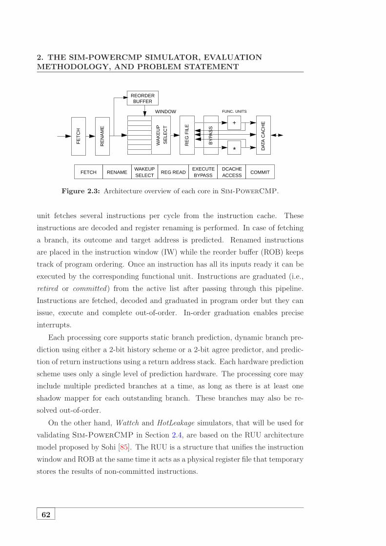
2. THE SIM-POWERCMP SIMULATOR, EVALUATIONMETHODOLOGY, AND PROBLEM STATEMENT
FE
TC
H
RE
NA
ME
REORDERBUFFER
WAKEUPSELECT
FETCH RENAME REG READ COMMIT
WA
KE
UP
SE
LEC
T
RE
GF
ILE
DAT
AC
AC
HE
WINDOW FUNC. UNITS
+
*
EXECUTEBYPASS
DCACHEACCESS
BY
PAS
S
Figure 2.3: Architecture overview of each core in Sim-PowerCMP.
unit fetches several instructions per cycle from the instruction cache. These
instructions are decoded and register renaming is performed. In case of fetching
a branch, its outcome and target address is predicted. Renamed instructions
are placed in the instruction window (IW) while the reorder buffer (ROB) keeps
track of program ordering. Once an instruction has all its inputs ready it can be
executed by the corresponding functional unit. Instructions are graduated (i.e.,
retired or committed) from the active list after passing through this pipeline.
Instructions are fetched, decoded and graduated in program order but they can
issue, execute and complete out-of-order. In-order graduation enables precise
interrupts.
Each processing core supports static branch prediction, dynamic branch pre-
diction using either a 2-bit history scheme or a 2-bit agree predictor, and predic-
tion of return instructions using a return address stack. Each hardware prediction
scheme uses only a single level of prediction hardware. The processing core may
include multiple predicted branches at a time, as long as there is at least one
shadow mapper for each outstanding branch. These branches may also be re-
solved out-of-order.
On the other hand, Wattch and HotLeakage simulators, that will be used for
validating Sim-PowerCMP in Section 2.4, are based on the RUU architecture
model proposed by Sohi [85]. The RUU is a structure that unifies the instruction
window and ROB at the same time it acts as a physical register file that temporary
stores the results of non-committed instructions.
62

2.3 The Sim-PowerCMP Simulator
Table 2.1: Main processing core parameters and their selected values.
Processing Core
Processor Speed 4 GHz
Max. fetch/retire rate 2 (in-order)
Active List 32
Functional Units 2 integer arithmetic
2 floating point
2 address generation
Branch Predictor 2-bit history predictor
Counters in the Branch Predictor Buffer 512
Shadow Mappers 8
Memory queue size 32 entries
There are two major differences between the two models. The first difference
is that in the architecture model of Fig. 2.3 (followed by the MIPS R10000, RSIM
and Sim-PowerCMP), all computed values, speculative or not, are stored in the
register file. However, in Sohi’s model, the RUU is responsible for temporary stor-
ing the non-committed output values while a separate register file is responsible
for storing the output values only when instructions have been committed and,
therefore, they are non-speculative values. The second major difference is that,
in Sim-PowerCMP architecture model, computed values are not sent to the in-
struction window, only the tags are sent for the tag match (or wake-up) process.
Computed values are sent to the register file. However, in Sohi’s model (used by
HotLeakage), all computed values are sent to the RUU and, therefore, dependent
instructions get their inputs from the RUU. These two architectural differences
must be taken into account when validating the proposed power model, as we
will show in next section.
Most processor parameters are user-configurable, including the number of
functional units, the latencies and repeat rates of the functional units, the in-
struction issue width, the size of the active list, the number of shadow mappers
for branch speculation, and the size of the branch prediction structures. Across
this Thesis, we usually model an in-order version of the R10000 (unless stated
differently). Table 2.1 presents some of the processor parameters.
63

2. THE SIM-POWERCMP SIMULATOR, EVALUATIONMETHODOLOGY, AND PROBLEM STATEMENT
2.3.2. Memory Hierarchy
Sim-PowerCMP simulates a cache-coherent tiled CMP architecture consist-
ing of arrays of replicated tiles connected over a switched direct network, with
variations of a full-map (or bit-vector) invalidation-based directory cache coher-
ence protocol. Each tile contains a processing core with primary caches (both
instruction and data caches), a slice of the L2 cache, and a connection to the
on-chip network. The L2 cache is shared among the different processing cores,
but it is physically distributed between them. Therefore, some accesses to the
L2 cache will be sent to the local slice while the rest will be serviced by remote
slices (L2 NUCA architecture [51]). In addition, the L2 cache stores (in the tags’
part of the local L2 slice) the directory information needed to ensure coherence
between the L1 caches. As introduced before, on a L1 cache miss, a request
is sent down to the appropriate tile where further protocol actions are initiated
based on that block’s directory state, such as invalidation messages, intervention
messages, data writebacks, data block transfers, etc.
Both cache levels are lockup-free and store the state of outstanding requests
using miss status holding registers (MSHRs). The first-level cache can either be
a write-through cache with a non-allocate policy on writes, or a write-back cache
with a write-allocate policy. Sim-PowerCMP allows for a multiported and
pipelined first-level cache. Lines are replaced only on incoming replies. The size,
line size, set associativity, cache latency, number of ports, and number of MSHRs
can be varied. The coalescing write buffer is implemented as a buffer with cache-
line-sized entries. All writes are buffered there and sent to the second-level cache
as soon as this cache is free to accept a new request. The number of entries in
the write buffer is configurable. The second-level cache is a pipelined write back
cache with a write-allocate policy. Again, lines are replaced only on incoming
replies. The secondary cache maintains inclusion with respect to the first-level
cache. The size, set associativity, cache latency, and number of MSHRs can be
varied.
The directory information is stored in the tags’ part of the L2 cache slices. It
can support either a four-state MESI protocol with Modified, Exclusive, Shared
and Invalid states (similar to the one implemented in the SGI Origin 2000 [57]), or
64
2.3 The Sim-PowerCMP Simulator
a three-state MSI protocol. The Sim-PowerCMP directory protocol and cache
controllers support cache-to-cache transfers. The protocols also include transient
states at the directory and caches.
The interface for memory in a shared memory multiprocessor is called the
memory consistency model [1]. Sim-PowerCMP supports three memory con-
sistency models configurable at compile-time: sequential consistency, processor
consistency and release consistency.
Sequential consistency (SC) provides the most intuitive programming inter-
face for shared memory multiprocessors by requiring that all memory operations
appear to execute in program order and atomically [56]. On the other hand, re-
laxed consistency models have been shown to significantly outperform sequential
consistency for single-issue, statically scheduled processors with blocking reads.
However, current microprocessors aggressively exploit instruction-level paral-
lelism using methods such as multiple issue, dynamic scheduling and non-blocking
reads. This allows both relaxed and SC implementations to be more aggressive
and as established by Hill [38], “the future performance gap between the aggres-
sively relaxed models and sequential consistency will not be sufficient to justify
exposing the complexity of the aggressively relaxed models to the authors of low-
level software”.
In our particular case, we have configured Sim-PowerCMP to simulate se-
quential consistency following the guidelines given by Hill.
Table 2.2 illustrates the base values for the most important parameters of the
memory hierarchy.
2.3.3. Interconnection Network
For remote communication, Sim-PowerCMP currently supports a two-dimen-
sional mesh network. In particular, it models a wormhole-routed network with
contention at the various switches.
Most modern networks are deadlock-free as long as the modules on the net-
work continue to accept transactions. Within the network, this may require
restrictions on permissible routes or other special precautions, see [24] for details.
However, the network transactions used by request-response protocols (which are
65

2. THE SIM-POWERCMP SIMULATOR, EVALUATIONMETHODOLOGY, AND PROBLEM STATEMENT
Table 2.2: Main memory hierarchy parameters and their selected values.
Memory Hierarchy Parameters
Cache line size 64 bytes
L1 cache (on-chip, WT) Direct mapped, 32KB
L1 request ports 2
L1 hit time 1 cycle
L2 cache (on-chip, WB) 4-way associative, 256KB/core
L2 request ports 1
L2 hit time 6+2 cycles, pipelined
Number of MSHRs 8 per cache
Memory access time 400 cycles
Cache-coherence protocol MESI
Consistency model Sequential consistency
First coherence message creation time 1 cycle
Next coherence messages creation time 1 cycle
Table 2.3: Network’s main parameters and their selected values.
Network Parameters
Interconnection network 2D mesh
Network bandwidth 75 GB/s
Router parameters 3 stages (full pipeline)
2 VCs
32 flit buffers per input port
Link width 75 bytes (8X-B-Wires)
Link latency 4 cycles (full pipeline)
Link length 5 mm
intrinsic to a shared address space), could still cause deadlock situations and
Sim-PowerCMP provides two separate networks for requests and responses to
avoid them.
The flit delay per network hop, the width of the network, the buffer size at
each switch, and the length of each packet’s control header are user-configurable
parameters. In our simulations, we use a state-of-the-art network whose param-
eters are given in Table 2.3.
66

2.3 The Sim-PowerCMP Simulator
2.3.4. Sim-PowerCMP Power Model Overview
We have incorporated into Sim-PowerCMP already proposed and validated
power models for both dynamic power (from Wattch [13], CACTI [80]) and leak-
age power (from HotLeakage [99]) of each processing core, as well as the in-
terconnection network (from Orion [93]). Adapting the power models of the
main hardware structures of each core and the interconnection network to Sim-
PowerCMP is not a trivial task. The power modeling infrastructure used in
Wattch and HotLeakage is strongly coupled with the performance simulator code
and, although they are mostly parametrized power models, considerable effort
and deep understanding of the simulator implementation is needed in order to
port the power model infrastructure to Sim-PowerCMP. One major hurdle was
the extensive use of global variables to keep track of which units are accessed per
cycle in order to account for the total energy consumed by an application. In a
power-aware CMP simulator, these counters and statistics must be collected on
a per-core basis, and the use of global activity counters is forbidden. In order
to avoid rewriting the power model code used in these simulators we choose to
keep original global variables that are widely used across Wattch and HotLeakage
and define per core basis counters and partial/global power results. These values
are transferred to/from the global variables each time the power model functions
are called. In this way we were able to decouple the power model code borrowed
from Wattch and HotLeakage simulators.
On the other hand, the interconnection network power model used in Orion
is loosely coupled with the Liberty infrastructure in which the simulator is based,
making its integration with another performance simulator easier. However, some
additional changes were needed in order to make it fully interoperative with Sim-
PowerCMP. Specifically, Orion uses the power models defined in Wattch but
most of the constant values used in Wattch have been converted to parameters
that can be modified at execution time, making Orion more flexible. Therefore, it
was necessary to reconcile both approaches used to model the power dissipation.
Our decision was to use the more flexible aproach proposed by Orion, modifying
the header files where those constant values were defined.
67
2. THE SIM-POWERCMP SIMULATOR, EVALUATIONMETHODOLOGY, AND PROBLEM STATEMENT
Finally, we either changed some power models or derive new ones to match
several of the particularities of the CMP implemented in Sim-PowerCMP. For
instance, we needed to model the impact of the directory. In the CMP architec-
ture modeled in Sim-PowerCMP, the L2 cache stores the directory information
needed to ensure coherence between the L1 caches. So we changed the power
model of the L2 cache to account for both the extra storage bits and the extra
accesses to the directory.
2.4 Validation of the Power Model of Sim-PowerCMP
Validating power models is a crucial task to obtain reasonably accurate sim-
ulation results. We have used a validation methodology based on checking our
results against the ones obtained under the same configuration with other power
simulators that have already been validated and are widely used by the research
community: HotLeakage in the case of processor cores and Orion for the power
of the internal interconnection network.
Table 2.4 shows the configuration used to validate the power models used
in Sim-PowerCMP. It describes an 8-core CMP built in 65 nm technology.
The tile area has been fixed to 25 mm2, including a portion of the second-level
cache [98]. With this configuration, the links that interconnect the routers that
configure the 2D mesh topology would measure around 5 mm.
Table 2.5 shows an a priori comparison of the maximum dynamic power
breakdown for a core of the CMP using Sim-PowerCMP and HotLeakage. Note
that there are some differences for structures such as the rename logic, the register
file, and mainly, the instruction window. These differences are due to the different
superscalar architectures implemented in both simulators, as mentioned in the
previous section. HotLeakage simulator, based on SimpleScalar, implements the
RUU model that integrates the instruction window, ROB, and physical registers
in the same hardware structure. So, the power dissipation of the instruction
window (RUU for HotLeakage) is relatively high. It is important to note that the
main contribution to instruction window power dissipation is due to the accesses
to the physical registers (bitline-power in Table 2.5). In our Sim-PowerCMP
superscalar processor model, this power dissipation is zero. On the other hand,
68

2.4 Validation of the Power Model of Sim-PowerCMP
Table 2.4: Configuration of the CMP architecture used in the validation of the power
models of Sim-PowerCMP.
Core Configuration
Parameter HotLeakage Sim-PowerCMP
Fetch/Issue/Commit width 4
Active List — 64
Instr. window (RUU) 32 —
Register File 32 64
Functional Units 2 IntALU, 2 FPALU
2 AddrGen, 2 mem ports
LSQ Entries 64
L1 I/D-Cache 32K, 4-way
L2 Cache (per core) 256K, 4-way, 10+20 cycles
Memory 400 cycles
Branch Pred. two-level, 4 K-entries
BTB 4 K-entries
CMP Parameters
Technology 65 nm
Core size 25 mm2
Number of cores 8
Interconnection network 2D mesh
Network bandwidth 75 GB/s
Router Parameters
Link length 5 mm
Flit size 75 Bytes
Buffer size 16 flits
69

2. THE SIM-POWERCMP SIMULATOR, EVALUATIONMETHODOLOGY, AND PROBLEM STATEMENT
Table 2.5: Dynamic power breakdown for the different structures in a processor core.
HotLeakage (W) Sim-PowerCMP (W)
Total Dynamic Power Consumption: 19.36 19.46
Branch Predictor Power Consumption: 0.82 4.72% 0.82 4.69%
Rename Logic Power Consumption: 0.08 0.49% 0.09 0.54%
Instruction Decode Power (W): 0.0040 0.0040
RAT decode power (W): 0.0316 0.0316
RAT wordline power (W): 0.0085 0.0097
RAT bitline power (W): 0.0386 0.0463
DCL Comparators (W): 0.0023 0.0023
Instruction Window Power Consumption: 0.52 3.01% 0.07 0.39%
tagdrive (W): 0.0354 0.0425
tagmatch (W): 0.0169 0.0198
Selection Logic (W): 0.0068 0.0067
decode power (W): 0.0316 0
wordline power (W): 0.0205 0
bitline power (W): 0.4123 0
Load/Store Queue Power Consumption: 0.64 3.69% 0.64 3.67%
Arch. Register File Power Consumption: 0.46 2.68% 0.82 4.68%
decode power (W): 0.0316 0.0653
wordline power (W): 0.0205 0.0205
bitline power (W): 0.4123 0.7308
Result Bus Power Consumption: 0.77 4.44% 1.02 5.85%
Total Clock Power: 7.30 42.07% 7.24 41.49%
Int ALU Power: 1.55 8.91% 1.55 8.87%
FP ALU Power: 2.37 13.66% 2.37 13.58%
Instruction Cache Power Consumption: 0.67 3.88% 0.67 3.86%
Itlb power (W): 0.05 0.29% 0.05 0.28%
Data Cache Power Consumption: 1.35 7.77% 1.35 7.72%
Dtlb power (W): 0.17 0.97% 0.18 0.96%
Level 2 Cache Power Consumption: 0.59 3.43% 0.59 3.41%
Ambient Power Consumption: 2.00 10.33% 2.00 10.28%
70

2.4 Validation of the Power Model of Sim-PowerCMP
LOG
ICA
LR
EG
IST
ER
ID
WORDLINE
BIT
LIN
E
SENSEAMPLIFIER
DE
CO
DE
R
PHYSICAL TAG BIT
ROW0
ROW1
ROW NVREG −1
SHIFTREG
CELL
READ PORTWRITE PORT
WORDLINES
BIT
LIN
ES
ACCESS STACK
Figure 2.4: Mapping table of the rename logic (left). Single cell of the mapping table
(right).
Table 2.6: Static power dissipation for regular structures of a processor core.
HotLeakage Sim-PowerCMP
Total Static Power Consumption (W): 0.23812 0.24665
Arch. Register File Power Consumption: (W) 0.00449 0.00898
Instruction Cache Power Consumption: (W) 0.02397 0.02397
Data Cache Power Consumption: (W) 0.02397 0.02397
Level 2 Cache Power Consumption: (W) 0.18974 0.18974
the model used in Sim-PowerCMP requires to duplicate the size of the register
file because it keeps both speculative and non-speculative result values (logical
and physical registers). This explains the higher power dissipation in the register
file (as shown in the Table 2.5). The slightly higher power dissipation in the
rename logic is due to the fact that physical register tags have one additional bit
in Sim-PowerCMP model because we double the size of the register file, as it
can be observed in Fig. 2.4.
Table 2.6 shows the static power dissipation for the main regular hardware
structures in a core. The only difference is found in the register file because of
the bigger size in our Sim-PowerCMP.
After this a priori analysis of the maximum power dissipation for a core, the
71

2. THE SIM-POWERCMP SIMULATOR, EVALUATIONMETHODOLOGY, AND PROBLEM STATEMENT
Table 2.7: Percentage of committed instructions in both test programs.
Test 1 Test 2
HotLeakage PowerCMP HotLeakage PowerCMP
Arithmetic-logical 54.10% 54.17% 55.58% 61.92%
Data transfer 41.71% 41.67% 38.86% 33.31%
Unconditional jump 0% 0% 0% 0%
Conditional branch 4.18% 4.17% 4.56% 4.77%
next step in the validation of the power model is to compare the dynamic power
dissipation when real programs are simulated. However, it is important to note
that both simulators use different instruction set architectures (SPARC and PISA
ISAs for Sim-PowerCMP and Hotleakage, respectively) which complicates the
comparison. Furthermore, the use of different compilers as well as slightly differ-
ent optimization flags can appreciably change the instruction mix for a program.
Therefore, we decided to use a two-step validation strategy, initially using very
simple test programs in order to obtain a preliminary validation. Then, we per-
formed the final validation using some of the SPEC-2000 applications [37].
A preliminary validation using microbenchmarks has two advantages: (1) the
percentage of memory accesses, arithmetic-logic and control instructions are very
similar when we use these simple programs, even when the ISAs are different,
allowing an easier comparison of dynamic power dissipation; (2) the generated
code is simple enough to predict which core structures are the main contribu-
tors to dynamic power dissipation, in order to explain the sources of potential
discrepancies.
The test programs used for the preliminary power model validation were two
microbenchmarks written in C and compiled using PISA (HotLeakage simulator)
and SPARC (Sim-PowerCMP simulator) versions of the gcc compiler. The op-
timization options activated in both cases were -O3 -funroll-loops. The first
test performs a sequential access to an array of integers, accumulating all the val-
ues into a global variable, whereas the second one implements the multiplication
of two matrices of doubles. Table 2.7 shows the percentage of instructions that
are committed in both cases. Even with these simple codes and using the same
72

2.4 Validation of the Power Model of Sim-PowerCMP
Table 2.8: Dynamic power dissipation for a core after simulating both microbench-
marks.
Test 1 Test 2
Avg. access/c Avg. power (W) Avg. access/c Avg. power (W)
HL SPcmp HL SPcmp HL SPcmp HL SPcmp
Rename Table 2.40 2.30 0.05 0.05 2.86 2.57 0.06 0.06
Branch prediction 0.10 0.10 0.11 0.11 0.16 0.14 0.13 0.13
Instruction window 9.19 4.70 0.52 0.04 10.59 5.57 0.55 0.05
LSQ 1.00 1.00 0.28 0.28 1.27 1.28 0.26 0.25
Register file 3.50 5.80 0.13 0.38 4.25 7.14 0.16 0.46
L1 i-cache 2.40 2.40 0.72 0.72 2.86 3.00 0.70 0.72
L1 d-cache 1.00 1.00 0.79 0.80 0.84 0.86 0.73 0.69
Int + FP ALU 2.40 2.40 1.17 1.17 2.85 2.99 1.73 1.72
Result bus 3.30 3.30 0.64 0.58 3.49 3.57 0.64 0.63
Clock 2.51 2.84 3.24 3.44
Fetch stage 0.84 0.84 0.86 0.85
Dispatch stage 0.05 0.05 0.06 0.06
Issue stage 3.47 2.94 3.93 3.39
Avg. power/cycle 7.24 7.08 8.25 8.21
Avg. power/instr. 3.40 3.42 3.49 3.31
Max power/cycle 9.63 9.26 12.12 11.49
compiler with the same optimization options, the obtained percentages are not
exactly the same, but are very similar. To perform the comparison we used the
power model cc3 defined in [13], which implements a clock-gating scheme that
adjusts the dynamic power based on resource utilization3.
Table 2.8 shows the results obtained after completing the simulation for both
microbenchmarks under perfect cache assumption. It can be observed that re-
sults are almost identical, except for the register file and the instruction window.
These differences are related with the particular microarchitecture modeled by
each simulator. As explained before, the main contribution to instruction win-
dow power consumption is due to the accesses to the physical registers. In the
3If a multiported unit is used in a clock cycle, its maximum power dissipation (Table 2.5)
is scaled linearly with port usage. Unused units in a clock cycle are supposed to still dissipate
10% of their maximum power, rather than drawing zero power.
73

2. THE SIM-POWERCMP SIMULATOR, EVALUATIONMETHODOLOGY, AND PROBLEM STATEMENT
model implemented in Sim-PowerCMP, these acesses are done to the register
file that now keeps both speculative and non-speculative result values (logical
and physical registers). This explains the higher average acceses per cycle and
power consumption in the register file for Sim-PowerCMP as well as the un-
derutilization of the instruction window compared with the results obtained for
the HotLeakage simulator.
The second step of our power model validation methodology consisted in com-
paring the results obtained after running a subset of the SPEC-2000 applications.
In these simulations we still assume perfect L1 caches in order to avoid interfer-
ences due to the different implementations of the memory hierarchy in both simu-
lators. Fig. 2.5 shows the dynamic power dissipation as well as the IPC obtained
for each application. In general, we obtain the same power distribution among
the different hardware structures of a core, although there are some differences
that are worth to explain.
Firstly, we observe higher power dissipation in a core for HotLeakage, due
to the fact that for the same applications the IPC obtained in this simulator
is usually higher due to the different instruction set architectures used in both
simulators. The higher the IPC, the higher the number of accesses per cycle to
the different hardware structures that are modeled. This leads to an increase in
the dynamic power of these structures. For the mcf application, where the IPC
obtained in both simulators is similar, power dissipation is very close. Finally,
if we analyze the power distribution for Sim-PowerCMP, we can appreciate a
considerable drop in the power dissipated by the instruction window, partially
compensated by the higher power dissipation in the register file. The reason to
this global dynamic power drop is the different types of processor cores modeled
inside each simulator, as previously discussed.
Once we finished the validation of the power model associated with each core
of the CMP, the next step was to validate the power model of the interconnection
network. Fig. 2.6 shows the distribution of the power dissipation for routers
that implement the 2D-mesh. For our modeled routers, 62% of the total power
comes from the link circuitry. This value is similar to the 60% dissipated by links
in the Alpha 21364 routers and a little lower than the 82% cited in [79]. The
power dissipated by the links strongly depends on the amount of buffer space
74
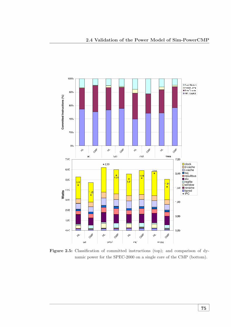
2.4 Validation of the Power Model of Sim-PowerCMP
Figure 2.5: Classification of committed instructions (top); and comparison of dy-
namic power for the SPEC-2000 on a single core of the CMP (bottom).
75

2. THE SIM-POWERCMP SIMULATOR, EVALUATIONMETHODOLOGY, AND PROBLEM STATEMENT
Figure 2.6: Distribution of the power dissipation inside a router.
assigned to the router compared with channel bandwidth. Our results also agree
with the results reported in [94], with a maximum power dissipation of 2-3 W
per router inside a CMP (excluding link circuitry). With this power data, the
interconnection network takes about 20-30% of the total CMP power budget, as
published in different works [79; 94].
As conclusion, we have compared the results obtained when several appli-
cations are simulated in both Sim-PowerCMP and HotLeakage in order to
validate the power models implemented in our simulation framework. As ex-
pected, some differences were observed mainly due to the different architecture
organization modeled in both simulators as well as the different instruction set ar-
chitectures. Moreover, the overall distribution of the power consumption among
the main hardware structures presented in a tiled chip-multiprocessor agree with
the results reported by different researchers [66; 79; 94].
2.5 Benchmarks
Here, we describe the ten benchmark programs used to evaluate the optimiza-
tions proposed in this Thesis. The selected benchmarks are presented in Table 2.9
and cover a variety of computation and communication patterns. Barnes-Hut,
FFT, LU-Cont, LU-Nonc,Ocean-Cont,Ocean-Nonc,Radix, Raytrace,
Water-SPA and Water-NSQ are from the SPLASH-2 benchmark suite [96].
EM3D is a shared memory implementation of the Split-C benchmark [53]. MP3D
76

2.5 Benchmarks
Table 2.9: Benchmarks and input sizes used in this work.
Benchmark Input Size
Barnes-Hut 8192 bodies, 4 time steps
EM3D 38400 nodes, degree 2, 15% remote and 25 time steps
LU-cont 256× 256, B=8
LU-Nonc 256× 256, B=8
FFT 256K complex doubles
MP3D 48000 nodes, 20 time steps
Ocean-Cont 258x258 ocean
Ocean-Nonc 258x258 ocean
Radix 2M keys, 1024 radix
Raytrace car.env
Unstructured Mesh.2K, 5 time steps
Water-NSQ 512 molecules, 4 time steps
Water-SPA 512 molecules, 4 time steps
application is drawn from the SPLASH suite [81]. Finally, Unstructured is a
computational fluid dynamics application [69].
All experimental results reported in this Thesis correspond to the parallel
phase of these applications. Data placement in our programs is either done ex-
plicitly by the programmer or by RSIM which uses a first-touch policy on a
cache-line granularity. Thus, initial data-placement is quite effective in terms of
reducing traffic in the system. Problem sizes have been chosen commensurate to
the maximum number of processors used in each application.
2.5.1. BARNES-HUT
Barnes-Hut application simulates the interaction of a system of bodies
(galaxies or particles, for example) in three dimensions over a number of time
steps, using the Barnes-Hut hierarchical N -body method. Each body is modelled
as a point mass and exerts forces on all other bodies in the system. To speed up
the interbody force calculations, groups of bodies that are sufficiently far away
are abstracted as point masses. In order to facilitate this clustering, physical
space is divided recursively, forming an octree. The tree representation of space
77
2. THE SIM-POWERCMP SIMULATOR, EVALUATIONMETHODOLOGY, AND PROBLEM STATEMENT
has to be traversed once for each body and rebuilt after each time step to account
for the movement of bodies.
The main data structure in Barnes-Hut is the tree itself, which is imple-
mented as an array of bodies and an array of space cells that are linked together.
Bodies are assigned to processors at the beginning of each time step in a par-
titioning phase. Each processor calculates the forces exerted on its own subset
of bodies. The bodies are then moved under the influence of those forces. Fi-
nally, the tree is regenerated for the next time step. There are several barriers for
separating different phases of the computation and successive time steps. Some
phases require exclusive access to tree cells and a set of distributed locks is used
for this purpose. The communication patterns are dependent on the particle dis-
tribution and are quite irregular. No attempt is made at intelligent distribution
of body data in main memory, since this is difficult at page granularity and not
very important to performance.
2.5.2. EM3D
EM3D models the propagation of electromagnetic waves through objects in
three dimensions. The problem is framed as a computation on a bipartite graph
with directed edges from E nodes, representing electric fields, to H nodes, rep-
resenting magnetic fields, and vice versa. At each step in the computation, new
E values are first computed from the weighted sum of neighboring H nodes, and
then new H values are computed from the weighted sum of neighboring E nodes.
Edges and their weights are determined statically.
The initialization phase of EM3D builds the graph and does some precom-
putation to improve the performance of the main loop. To build the graph, each
processor allocates a set of E nodes and a set of H nodes. Edges are randomly gen-
erated using a user-specified percentage that determines how many edges point
to remote graph nodes. The sharing patterns found in this application are static
and repetitive.
78

2.5 Benchmarks
2.5.3. FFT
The FFT kernel is a complex 1-D version of the radix-√n six-step FFT algo-
rithm, which is optimized to minimize interprocessor communication. The data
set consists of the n complex data points to be transformed, and another n com-
plex data points referred to as the roots of unity. Both sets of data are organized
as√n ×
√n matrices partitioned so that every processor is assigned a contigu-
ous set of rows which are allocated in its local memory. Synchronization in this
application is accomplished by using barriers.
2.5.4. LU
The LU kernel factors a dense matrix into the product of a lower triangular
and an upper triangular matrix. The dense n × n matrix A is divided into an
N×N array of B×B blocks (n = NB ) to exploit temporal locality on submatrix
elements. To reduce communication, block ownership is assigned using a 2-D
scatter decomposition, with blocks being updated by the processors that own
them. The block size B should be large enough to keep the cache miss rate low,
and small enough to maintain good load balance. Fairly small block sizes (B =8
or B=16) strike a good balance in practice. Elements within a block are allocated
contiguously to improve spatial locality benefits, and blocks are allocated locally
to processors that own them.
2.5.5. MP3D
MP3D is a Monte Carlo simulation of rarefied fluid flow. This benchmark
simulates the hypersonic flow of particles at extremely low densities.
Succinctly, MP3D simulates the trajectories of particles through an active
space and adjusts the velocities of the particles based on collisions with the bound-
aries (such as the wind tunnel walls) and other particles. After the system reaches
steady-state, statistical analysis of the trajectory data produces an estimated flow
field for the studied configuration. MP3D finds collision partners efficiently by
representing the active space as an array of three-dimensional unit-sized cells.
Only particles present in the same cell at the same time are eligible for collision
79

2. THE SIM-POWERCMP SIMULATOR, EVALUATIONMETHODOLOGY, AND PROBLEM STATEMENT
consideration. If the application finds an eligible pair, it uses probabilistic test
to decide whether a collision actually occurs.
MP3D allocates work to each process through a static assignment of the
simulated particles. Each simulated step consists of a move phase and a collide
phase for each particle that the process owns. The move phase computes the
particle’s new position based both on its current position and velocity, and its
interaction with boundaries. The collision phase determines if the particle just
moved collides with another particle, and if so, adjusts the velocities of both
particles. Data sharing occurs during collisions and through accesses to the unit-
sized space cells. During a collision, a process may have to update the position and
velocity of a particle owned by another process. Also, each space cell maintains
a count of the particle population currently present in that cell. Therefore, each
time a process moves a particle, it may have to update the population count
of some space cells if that particle passes from one cell to another. These data
accesses to particles and space cells may lead to race conditions that optional locks
eliminate at some performance cost. In this Thesis, MP3D is compiled with these
locks. The presence of locks typically slow down the application execution but
eliminates the data races and allows repeatability of the results.
2.5.6. OCEAN
The Ocean application studies large-scale ocean movements based on eddy
and boundary currents. The algorithm simulates a cuboidal basin using dis-
cretized circulation model that takes into account wind stress from atmospheric
effects and the friction with ocean floor and walls. The algorithm performs the
simulation for many time steps until the eddies and mean ocean flow attain a
mutual balance. The work performed every time step essentially involves setting
up and solving a set of spatial partial differential equations. For this purpose, the
algorithm discretizes the continuous functions by second-order finite-differencing,
sets up the resulting difference equations on two-dimensional fixed-size grids rep-
resenting horizontal cross-sections of the ocean basin, and solves these equations
using a red-back Gauss-Seidel multigrid equation solver. Each task performs the
80

2.5 Benchmarks
computational steps on the section of the grids that it owns, regularly communi-
cating with other processes.
2.5.7. RADIX
The Radix program sorts a series of integers, called keys, using the popular
radix sorting method. The algorithm is iterative, performing one iteration for each
radix r digit of the keys. In each iteration, a processor passes over its assigned keys
and generates a local histogram. The local histograms are then accumulated into
a global histogram. Finally, each processor uses the global histogram to permute
its keys into a new array for the next iteration. This permutation step requires
all-to-all communication. The permutation is inherently a sender-determined one,
so keys are communicated through writes rather than reads. Synchronization in
this application is accomplished by using barriers.
2.5.8. RAYTRACE
This application renders a three-dimensional scene using ray-tracing. A hier-
archical uniform grid (similar to an octree) is used to represent the scene, and
early ray termination and antialiasing are implemented, although antialiasing is
not used in this study. A ray is traced through each pixel in the image plane,
and reflects in unpredictable ways off the objects it strikes. Each contact gener-
ates multiple rays, and the recursion results in a ray tree per pixel. The image
plane is partitioned among processors in contiguous blocks of pixel groups, and
distributed task queues are used with task stealing. The major data structures
represent rays, ray trees, the hierarchical uniform grid, task queues, and the prim-
itives that describe the scene. The data access patterns are highly unpredictable
in this application.
2.5.9. UNSTRUCTURED
Unstructured is a computational fluid dynamics application that uses an
unstructured mesh to model a physical structure, such as an airplane wing or
body. The mesh is represented by nodes, edges that connect two nodes, and faces
81

2. THE SIM-POWERCMP SIMULATOR, EVALUATIONMETHODOLOGY, AND PROBLEM STATEMENT
that connect three or four nodes. The mesh is static, so its connectivity does
not change. The mesh is partitioned spatially among different processors using a
recursive coordinate bisection partitioner. The computation contains a series of
loops that iterate over nodes, edges and faces. Most communication occurs along
the edges and faces of the mesh.
2.5.10. WATER-NSQ
Water-NSQ performs an N -body molecular dynamics simulation of the
forces and potentials in a system of water molecules. It is used to predict some
of the physical properties of water in the liquid state.
Molecules are statically split among the processors and the main data struc-
ture in Water-NSQ is a large array of records that is used to store the state of
each molecule. At each time step, the processors calculate the interaction of the
atoms within each molecule and the interaction of the molecules with one another.
For each molecule, the owning processor calculates the interactions with only half
of the molecules ahead of it in the array. Since the forces between the molecules
are symmetric, each pair-wise interaction between molecules is thus considered
only once. The state associated with the molecules is then updated. Although
some portions of the molecule state are modified at each interaction, others are
only changed between time steps. There are also several variables holding global
properties that are updated continuously.
2.5.11. WATER-SPA
This application solves the same problem as Water-NSQ, but uses a more
efficient algorithm. It imposes a uniform 3-D grid of cells on the problem domain,
and uses an O(n) algorithm which is more efficient than Water-NSQ for large
numbers of molecules. The advantage of the grid of cells is that processors which
own a cell only need to look at neighboring cells to find molecules that may
be within the cutoff radius of molecules in the box it owns. The movement
of molecules into and out of cells causes cell lists to be updated, resulting in
communication.
82

2.5 Benchmarks
Table 2.10: Summary of the problem sizes, maximum number of processors that can
be used, total number of memory lines that are referenced and dominant
sharing patterns for the benchmarks used in this Thesis.
Benchmark Problem Max Memory Dominant Sharing
Size Processors lines Patterns
Barnes-Hut 8192 bodies 64 22.32 K Wide sharing
EM3D 38400 nodes 64 120.55 K Producer-consumer
FFT 256K complex doubles 64 200.87 K Producer-consumer
LU-Cont 256× 256, B=8 64 69.12 K Regular
LU-Nonc 256× 256, B=8 64 69.12 K Regular
MP3D 48000 nodes 64 30.99 K Migratory
Ocean-Cont 258x258 ocean 32 248.48 K Producer-consumer
Ocean-Nonc 258x258 ocean 32 248.48 K Producer-consumer
Radix 2M keys 64 276.30 K Producer-consumer
Raytrace car.env 64 Highly unpredictable
Unstructured Mesh.2K 32 13.54 K Producer-consumer
and migratory
Water-NSQ 512 molecules 64 71.81 K Migratory
Water-SPA 512 molecules 64 5.85 K Wide sharing
2.5.12. Summary of Applications Used in Our Experi-
ments
Table 2.10 summarizes the main characteristics of the applications used in
our evaluations. For each application, it shows the problem size that has been
selected, the maximum number of processors that can be used, the size of the
resulting working set as well as the dominant sharing patterns that are found. As
in [49], three main sharing patterns have been considered: migratory, producer-
consumer and widely-sharing data.
Barnes-Hut is an example of a program with little widely-shared data. The
top of the octree is widely shared. However, it is difficulty to determine statically
how many levels of the octree are widely shared [49]. Another application showing
widely-shared data is Water-SPA.
On the other hand, migratory sharing constitutes the main sharing pattern
found in Water-NSQ. Also, the two arrays used in MP3D (the particle array
83

2. THE SIM-POWERCMP SIMULATOR, EVALUATIONMETHODOLOGY, AND PROBLEM STATEMENT
and the space array) constitute migratory data [49].
The dominant sharing patterns found in Ocean and Radix are producer-
consumer [42; 49]. FFT is an intensive bandwidth application that also exhibits
a producer-consumer sharing pattern. Finally, the nodes in the graph used in
EM3D have a producer-consumer relationship [18].
Unstructured is different from the rest of applications because it has dif-
ferent dominant patterns for the same data structures in different phases of the
application. The same data structures oscillate between migratory and producer-
consumer sharing patterns [68].
2.6 Evaluating the Energy-Efficiency of CMP Archi-
tectures
In this section, we focus on the characterization of the energy-efficiency of
the interconnection network in future CMP architectures. First, a breakdown
of the power dissipated in a CMP is presented. Then, the contribution of the
different types of messages to the interconnect power consumption is analyzed.
Finally, Fig. 2.7 presents a breakdown of the power dissipated in an 8- and 16-
core CMP. Total power dissipation is split among the most important structures
of the CMP (for the sake of legibility we have omitted the contribution of the
clock). As expected, it can be observed that most of the power is dissipated
in the processor cores of the CMP. In particular, the ALU reveals as one of the
most consuming structures of the CMP, as reported in [66]. Regarding the caches
(private L1 caches and the shared multibanked L2 cache) we can see that their
fraction of the total power is quite significant. Additionally, we see that in this
case most of the power is dissipated in the first-level instruction and data caches.
Fig. 2.7 also shows that the contribution of the interconnection network to the
total power is close to 20% on average, with several applications reaching up
to 30%. In this case, we have observed that most of this power is dissipated
in the point-to-point links used to configure the interconnect. In the literature
it can be found a plethora of techniques and proposals aimed at reducing the
energy consumption of the main core structures, however, the impact that the
84

2.6 Evaluating the Energy-Efficiency of CMP Architectures
Figure 2.7: Breakdown of the power dissipation in an 8-core (top) and 16-core CMP
(bottom) for several parallel scientific applications (the contribution of
the clock logic is not included for clarity).
85

2. THE SIM-POWERCMP SIMULATOR, EVALUATIONMETHODOLOGY, AND PROBLEM STATEMENT
Replacement
Cohe response
Response
Request
Cohe command
TypeDestSrc MSHR Cache Block
Dest ControlSrc Type Address
TypeDestSrc MSHR
Dest ControlSrc Type Address
TypeDestSrc MSHR
Cache Block
Dest ControlSrc Type Address
Dest ControlSrc Type Address Cache Block
TypeDestSrc MSHR
Figure 2.8: Classification of messages that travel on the interconnection network of a
tiled CMP architecture.
interconnection network has on total energy consumption is very significant and
techniques aimed at optimizing the delivery of messages through the interconnect
should be the goal of current research efforts.
For these reasons, this Thesis focuses on techniques aimed at increasing both
the performance and the energy-efficiency of the interconnection network in fu-
ture CMP architectures. For this purpose, it would be helpful to analyze how
this power distributes among the different types of messages that travel on the
interconnect.
2.6.1. Classification of Messages in Tiled CMP Architec-
tures
There is a variety of message types traveling on the interconnect of a CMP,
each one with properties that are clearly distinct. In general, messages can be
classified into the following groups (see Fig. 2.8):
1. Request messages, that are generated by cache controllers in response to
L1 cache misses. Requests are sent to the corresponding home L2 cache to
demand privileges (read-only or read/write) over a memory line.
86

2.6 Evaluating the Energy-Efficiency of CMP Architectures
Figure 2.9: Breakdown of the messages that travel on the interconnection network
for a 16-core CMP.
2. Response messages, that are sent in response to requests. These messages
can be generated by the home L2 cache controller or, alternatively, by the
remote L1 cache that has the single valid copy of the data, and they can
carry the memory line or not. The latter is due to the presence of upgrade
requests used to demand ownership for a line already kept in the local L1
cache.
3. Coherence commands, that are sent by the home L2 cache controller to
the corresponding L1 caches to ensure coherence (for example, invalidation
messages).
4. Coherence responses, sent by the L1 caches back to the corresponding
home L2 in response to coherence commands.
5. Replacement messages, that L1 caches generate in case of exclusive or
modified lines being replaced.
87

2. THE SIM-POWERCMP SIMULATOR, EVALUATIONMETHODOLOGY, AND PROBLEM STATEMENT
Fig. 2.9 shows the fraction of each message type over the total number of
messages for a 16-core CMP configuration for the applications used in our evalu-
ation. As it can be seen, on average, more than 60% of the messages are related
to memory accesses (a request and its corresponding reply), whereas the rest
has to do with coherence enforcement (25%) and block replacement (15%). It is
interesting to note that almost all replies imply the transfer of memory blocks
(Resp.+Data).
Alternatively, messages involved in the L1 cache coherence protocol shown in
Fig. 2.9 can be classified according to their criticality into critical and non-critical
messages. We say that a message is critical when it is in the critical path of the L1
cache miss. In other case, we call the message non-critical. As expected, delaying
a critical message will result in longer L1 cache miss latencies. On the other
hand, slight slowdowns in the delivery of non-critical messages will not cause any
performance degradation.
As an example, Fig. 2.10 shows the coherence actions involved in a L1 read
miss for a line in modified state in other tile. These actions consist of: (1) a
request message that is sent down to the appropriate directory tile (the home
L2 cache); (2) an intervention message sent to the owner tile that sends back
the line (3a) to the requestor and to the directory tile (3b). Whereas messages
(1), (2) and (3a) are critical because they belong to the critical path between the
processor request and the memory system response, (3b) is non-critical. Using
this criterion, we can observe that all message types but replacement messages
and some coherence replies (such as revision messages) are critical. It is clear that
performance will be increased if critical messages are sent through low-latency
L-Wires (assuming that there are enough wires). At the same time energy will
be saved, without affecting performance, when non-critical messages travel on
slower, power-efficient PW-Wires, as we will show in the next chapter.
On the other hand, coherence messages can also be classified according to their
size into either short or long messages. Coherence responses do not include the ad-
dress or the data block and just contain control information (source/destination,
message type, MSHR id, etc). In this way, we can say that they are short mes-
sages. Other message types, in particular requests and coherence commands, also
contain address block information but they are still narrow enough to be classified
88

2.6 Evaluating the Energy-Efficiency of CMP Architectures
OHR
1: Read request 2: Intervention
3b: Revision
3a: Ordinary Reply
Figure 2.10: Protocol actions taken in response to a read request that misses for a
block in modified state (messages with data are represented using thicker
lines).
Figure 2.11: Percentage of the power dissipated in the interconnection network by
each message type for a 16-core CMP.
as short messages. Finally, replacements with data and data block transfers also
carry a cache line and, therefore, they are classified as long messages.
Regarding the power dissipated by each message type, Fig. 2.11 plots their
power breakdown for the baseline configuration using only B-Wires. As it can be
seen, most of the power in the interconnect is associated to reply messages that
carry L2 cache lines (55%-65%). As previously commented, most of this power is
dissipated in the point-to-point links and, therefore, message size plays a major
89

2. THE SIM-POWERCMP SIMULATOR, EVALUATIONMETHODOLOGY, AND PROBLEM STATEMENT
Table 2.11: Classification of the messages that travel on the interconnection network
according to their criticality and length.
Message Type Critical? Length Preferred Wires
(assuming unbounded number)
Request Yes Short L-Wires
Response Yes Short/Long L-Wires (Performance)
PW-Wires (Energy)
Cohe. Command Yes Short L-Wires
Cohe. Replies Yes/No Short L-Wires (Critical)
PW-Wires (Non-critical)
Replacements No Short/Long PW-Wires
role.
The use of a heterogeneous interconnect comprised of low-latency L-Wires
and power-efficient PW-Wires allows for a more energy-efficient interconnect uti-
lization. However, as the number of L-Wires is smaller because of their four-fold
area cost (relative to baseline wires) only short messages can take full advantage
of them. On the other hand, since message size has direct impact on the power
dissipated in the interconnect, significant energy savings can be obtained when
long messages are sent through PW-Wires.
Table 2.11 summarizes the characteristics of each message type (in terms of
criticality and length) and points out the links that would be preferred in every
case. In general, short messages are critical and, therefore, should be sent through
L-Wires. The exceptions are coherence replies that are not in the critical path
of L1 cache misses (i.e., revision messages). On the other hand, long messages
can be critical (responses with data) or non-critical (replacements with data),
and the choice of wires to be used is not so clear in this case. If performance is
what matter the most (criticality), then L-Wires might be the best choice. On
the contrary, if energy is more important (length), then PW-Wires should be
utilized. In this way, the policy of sending critical messages on L-Wires and non-
critical on PW-Wires leaves the latter links underutilized since only replacements
would make use of them, and small energy savings would be obtained. On the
other hand, the policy of sending long messages on PW-Wires and short ones
on L-Wires causes important delays to responses with data, which would finally
90

2.6 Evaluating the Energy-Efficiency of CMP Architectures
translate into intolerable performance degradation.
In the next chapter, we will discuss how to take advantage of the different
characteristics of each message type (in terms of criticality and length) in or-
der to improve the energy efficiency and performace of the future dense CMP
architectures using heterogeneous networks.
91


3Heterogeneous Interconnects for
Energy-Efficient Message Management in
CMPs
3.1 Introduction
As discussed in the motivation of this Thesis (section 1.1), the high cost of
on-chip communication through global wires pose major performance and power
dissipation problems as technology shrinks and total die area increases [40]. This
trend will be exacerbated in future many-core CMP designs. In this chapter we
present our first proposal for dealing with the constraints that communication
impose for both high performance and energy efficiency in tiled CMPs.
Our proposal is aimed at achieving efficient message management, from the
point of view of both performance and energy, using two approaches. The first
one is Reply Partitioning, a technique that allows all messages used to ensure
coherence between the L1 caches of a CMP to be classified into two groups: a)
critical and short, and b) non-critical and long messages. The second approach is
the use of a heterogeneous interconnection network comprised of only two types of
wires: low-latency wires for critical messages and low-energy wires for non-critical
ones.
The main contribution of our proposal is the partitioning of reply messages
that carry data into a short critical message containing the sub-block of the cache
requested by the core as well as a long non-critical message with the whole cache
93

3. HETEROGENEOUS INTERCONNECTS FORENERGY-EFFICIENT MESSAGE MANAGEMENT IN CMPS
line. This partitioning allows for a more energy-efficient use of the heterogeneous
interconnect since now all short messages have been made critical whereas all
long messages have been made non-critical. The former can be sent through
the low-latency wires whereas the latter can be sent through the power-efficient
wires. Differently to proposals in [17], our proposed partitioning approach first,
eliminates a complex logic for choosing the correct set of wires (just based on
one bit in the message length field instead of checking the directory state or the
congestion level of the network) and second, it obtains significant energy-delay
improvements when using direct topologies. Additionally, our proposed approach
allows for a more balanced workload across the heterogeneous interconnect.
The rest of the chapter is organized as follows. The related work is given
in Section 3.2. Our proposal for efficient message management in tiled CMPs
is presented in section 3.3. Section 3.4 describes the evaluation methodology
and presents the results of the proposed mechanism. A sensitivity analysis is
presented in section 3.5. Finally, section 3.6 concludes the chapter.
3.2 Related Work
The on-chip interconnection network is a critical design element in a multi-core
architecture and, consequently, it has been the subject of several recent works.
Among others, Kumar et al. [55] analyze several on-chip interconnection mech-
anisms and topologies, and quantify their area, power, and latency overheads.
The study concludes that the design choices for the interconnect have a signifi-
cant effect on the rest of the chip, potentially consuming a significant fraction of
the real estate and power budget.
A reduced number of works have attempted to exploit the properties of a
heterogeneous interconnection network at the microarchitecture level in order to
reduce the interconnect energy share. Beckmann and Wood [8; 9] propose the
use of transmission lines to access large L2 on-chip caches in order to reduce the
required cache area and the dynamic power consumption of the interconnection
network. Nelson et al. [72] propose the use of silicon-based on-chip optical inter-
connects for minimizing the performance gap that the separation of the processing
94
3.2 Related Work
functions creates in a clustered architecture in an effort to alleviate power den-
sity. In [4], Balasubramonian et al. make the first proposal of wire management
at the microarchitecture level. They introduce the concept of a heterogeneous
interconnect that is comprised of wires with varying area, latency, bandwidth,
and energy characteristics, and they apply it to register communication within
a clustered architecture. In particular, cache accesses are accelerated by sending
a subset of the address bits on low-latency wires to prefetch data out of the L1
D-cache, while non-critical register values are transmitted on low-power wires.
Subsequently, they extend the proposal in [71] with new techniques aimed at ac-
celerating cache accesses in large L2/L3 split caches (L2/L3 NUCA architectures
[51]) by taking advantage of a lower-bandwidth, lower-latency network.
Cheng et al. [17] applied the heterogeneous network concept to the cache
coherence traffic problem in CMPs. In particular, they propose an interconnec-
tion network composed of three sets of wires with varying latency, bandwidth
and energy characteristics, and map coherence messages to the appropriate set
taking into account their latency and bandwidth needs. They report significant
performance improvement and interconnect energy reduction when a two-level
tree interconnect is used to connect the cores and the L2 cache. Unfortunately,
insignificant performance improvements were reported for direct topologies (such
as a D-torus).
More recently, Walter et al. [92] explore the benefits of adding a low latency,
customized shared bus as an integral part of the NoC architecture. This bus is
used for certain transactions such as broadcast of queries, fast delivery of control
signals, and quick exchange of small data items. Differently from our proposal,
they do not consider a directory-based CMP architecture when exploring the
benefits of their proposal over a traditional NoC architecture. In [11], the authors
propose a priority-based NoC which differentiates between short control signals
and long data messages to achieve a significant reduction in the cache access delay.
They also propose to use more efficient multicast and broadcast schemes instead
of multiple unicast messages in order to implement the invalidation procedure
and provide support for synchronization and mutual exclusion.
Finally, Balfour and Dally [5] evaluate a variety of on-chip networks designed
for 64-core tiled CMPs, and compare them in terms of performance, area and
95

3. HETEROGENEOUS INTERCONNECTS FORENERGY-EFFICIENT MESSAGE MANAGEMENT IN CMPS
energy efficiency. They conclude that a concentrated 4×4 mesh architecture (each
router is shared by four cores to reduce the hop count), replicated subnetworks
and express channels are the best option. Differently from our work, the authors
focus on the interconnection network design and obviate the cache coherence
protocol (they assume an abstract communication protocol).
3.3 Efficient Message Management in Tiled CMPs
As introduced before, there are two main components in our proposal. The
first one is Reply Partitioning, a technique that allows all messages used to ensure
coherence between the L1 caches of a CMP to be classified into two groups: a)
critical and short, and b) non-critical and long messages. The second approach is
the use of a heterogeneous interconnection network comprised of only two types of
wires: low-latency wires for critical messages and low-energy wires for non-critical
ones. This section starts describing the proposed Reply Partitioning mechanism.
Then, the architecture of the heterogeneous interconnect needed to implement
our proposal is presented.
3.3.1. Reply Partitioning for Decoupling Data Messages
into Critical and Non-Critical Parts
In this section we propose Reply Partitioning, a technique aimed at dealing
with reply messages that carry data. Reply Partitioning is based on the observa-
tion that when the processor requests data that is not found in the L1 cache (L1
cache miss), the full line could not be necessary in that moment but only a small
subset of it. In this way, our proposal splits replies with data into two messages.
The first is a short Partial Reply (PR) message that carries a sub-block of the
cache line that includes the word requested by the processor. And the second
message, called Ordinary Reply, is the original message and includes the full cache
line. Our proposal is inspired by the critical-word-first scheme for uniprocessors
described in [36] that requests the missed word first from memory and sends it to
the processor as soon as it arrives, letting the processor continue execution while
filling the remainder of the cache line.
96

3.3 Efficient Message Management in Tiled CMPs
Figure 3.1: Cumulative utilization of cache lines (top) and available time gap for
decoupling data messages (bottom) for a 16-core CMP.
97

3. HETEROGENEOUS INTERCONNECTS FORENERGY-EFFICIENT MESSAGE MANAGEMENT IN CMPS
Fig. 3.1 (top) shows the cumulative utilization of cache lines for a CMP with
16 cores. We can observe a high variability among applications, ranging from
applications where the common case is the access to a single word of the cache
line before an invalidation or replacement takes place (80% of the cases for the
Radix application) to applications as FFT and LU where the utilization of the
full line is the common case (over 90%). More interesting is Fig. 3.1 (bottom),
that measures the time between the first access to a cache line and a subsequent
access to a different word in the same cache line, as a good indicator of the
available time gap that we can take advantage of for decoupling replies with data.
Again, we observe a high variability among the applications. For applications such
as LU, Radix or Water-SPA, the number of cycles between the first access to
a cache line and a subsequent one to a different word is quite high so a good
behavior is expected for these applications with our Reply Partitioning proposal.
On the other hand, benchmarks such as FFT or Water-NSQ that show a very
low available time gap between subsequent cache accesses are expected to obtain
poor performance gains with our proposal.
It is important to note that the division of replies with data into Partial Replies
and Ordinary Replies makes all critical messages to be short (note that Partial
Replies are critical since they contain the word requested by the processor) and,
therefore, they can be sent using the low-latency L-Wires. At the same time,
all long messages become now non-critical (note that Ordinary Replies are non-
critical since the requested word also travels on a short message that hopefully will
arrive sooner) and, therefore, they can be sent using the power-efficient PW-Wires
without hurting performance. For a reply with data, performance improvements
will be obtained provided that the arrival time of the Ordinary Reply happens
within the time gap shown in Fig. 3.1 (bottom).
Fig. 3.2 shows the new behavior for the example discussed in Section 2.6.1
(Fig. 2.10) when Reply Partitioning is applied. We can observe that now all
messages belonging to the critical path between the processor request and the
memory system response are sent employing L-Wires, represented by solid lines.
At the same time, non-critical messages such as the revision to the directory tile
and the ordinary reply are sent using power-efficient PW-Wires, represented by
dashed lines in the figure.
98

3.3 Efficient Message Management in Tiled CMPs
OHR
1: Read request
3a2: Ordinary Reply
3b: Revision
2: Intervention
3a1: Partial Reply
Figure 3.2: New behavior for the case discussed in Fig. 2.10. The use of L-Wires is
represented by solid lines whereas dashed lines mean that power-efficient
PW-Wires are employed.
Additionally, splitting reply messages into a critical Partial Reply and a non-
critical Ordinary Reply has some implications over the coherence protocol. Recall
that, in a non-blocking cache, MSHR registers are used to keep track of outstand-
ing misses [54]. When the corresponding reply arrives, requests held in MSHR are
processed and the corresponding processor instructions are committed if needed.
In our mechanism, we have two different replies, and we need to define the ac-
tions required after the arrival of each one. Furthermore, with a 2D-mesh direct
interconnection network, the arrival order could not be guaranteed. That means
that, although unlikely, the non-critical Ordinary Reply could be received before
the critical Partial Reply1.
When a Partial Reply arrives we are sure that all coherence actions that en-
sure L1 cache coherence have been done. Therefore, after its arrival all awaiting
requests that can be satisfied are processed (e.g., read requests that hit in the
cache line sub-block and all write requests). For a read request, the corresponding
value is sent to the processor and, for a write request, the value is held in the
MSHR but the rest of hardware resources are released. In both cases, appropriate
processor instructions are committed. Only MSHR with non-processed read re-
quests and all the write requests, if any, are kept until the arrival of the Ordinary
Reply containing the full line. At the Ordinary Reply arrival time, the rest of
read requests are performed and the block is modified with the corresponding
1This could happen, for example, when adaptive routing is used.
99

3. HETEROGENEOUS INTERCONNECTS FORENERGY-EFFICIENT MESSAGE MANAGEMENT IN CMPS
write values held in the MSHR. In case of receiving the Ordinary Reply before
the Partial Reply, all requests waiting in the MSHR register are processed and
the corresponding instructions are committed; all hardware resources are released
but the MSHR, which is released when both replies arrive.
3.3.2. Designing the Interconnect for Efficient Message
Management
As discussed in section 1.1, L-Wires have a four-fold area cost compared to
baseline wires and, therefore, the number of L-Wires is quite limited. Considering
that they will be used for sending short, critical messages, the number of wires
should be fixed by considering the typical size of short messages. The remain-
ing area will be consumed by PW-Wires employed for sending long, non-critical
messages.
In this work, we use the same main parameters for the interconnect as in [17].
In particular, message sizes and the width of the original links of the interconnect
are the same. Short messages can take up to 11 bytes. Requests, coherence
commands and partial replies are 11-byte long since, beside control information
(3 bytes), they also carry address information (in the first two cases) or the sub-
block of data of one word size (for partial replies). On the other hand, coherence
replies are just 3-byte long. Replacements for lines in modified state are 75-
byte long since they carry both address (8 bytes) and a cache line (64 bytes)
in addition to control information (3 bytes). Finally, ordinary reply messages
are 67-byte long since they carry control information (3-bytes) and a cache line
(64 bytes). In order to match the metal area of the baseline configuration, each
original 75-byte unidirectional link (600 B-Wires) is designed to be made up of
88 L-Wires (11 bytes) and 248 PW-Wires (31 bytes)2.
The resulting design is similar to that proposed in [17], but with some impor-
tant differences. First of all, the election of the right set of wires for a message
does not require any additional logic since it can be made based exclusively on one
bit in the length field (some of the proposals developed in [17] require checking
of the directory state or tracking the congestion level in the network). Secondly,
288 (L-Wires) ×4 + 248 (PW-Wires) = 600 (B-Wires)
100

3.4 Experimental Results
the routing logic and the multiplexers and de-multiplexers associated with wires
are simpler since we only consider two types of wires instead of three. Finally,
our proposal achieves better levels of utilization of each set of wires (as we will
discuss in section 3.4.2.1).
3.4 Experimental Results
This section shows the results obtained for our proposal and compares them
against those achieved with two different configurations of the interconnect. The
first is the configuration that employs just B-Wires which is taken as baseline.
The second configuration is an implementation of the heterogeneous interconnect
presented in [17] that uses L-, B- and PW-Wires.
3.4.1. Evaluation Methodology
As we described in chapter 2, we have used thirteen benchmarks to evaluate
our proposals. The selected benchmarks cover a variety of computation and com-
munication patterns. Barnes-Hut, cholesky, FFT, Ocean, Radix, Ray-
trace, Water-SPA, and Water-NSQ from the SPLASH-2 benchmark suite
[96]. EM3D from the Split-C benchmark [53]. The MP3D application drawn
from the SPLASH suite [81]. And, finally, the computational fluid dynamics Un-
structured application [69]. Problem sizes have been chosen commensurate
with the size of the L1 caches and the number of cores used in our simulations,
following the recommendations given in [96]. All experimental results are for the
parallel phase of these applications (refer to section 2.5 for further benchmark
and working sets details).
Table 3.1 shows the relative area, delay, and power characteristics of L- and
PW-Wires compared to baseline wires (B-Wires) when a single metal plane is
considered (the 8X plane). For comparison purposes, the 3-subnetwork heteroge-
neous interconnect described in [17] was also implemented. In that configuration,
each link is comprised of three types of wires in two metal planes. Each wire type
has the area, delay, and power characteristics described in the foundation section
101
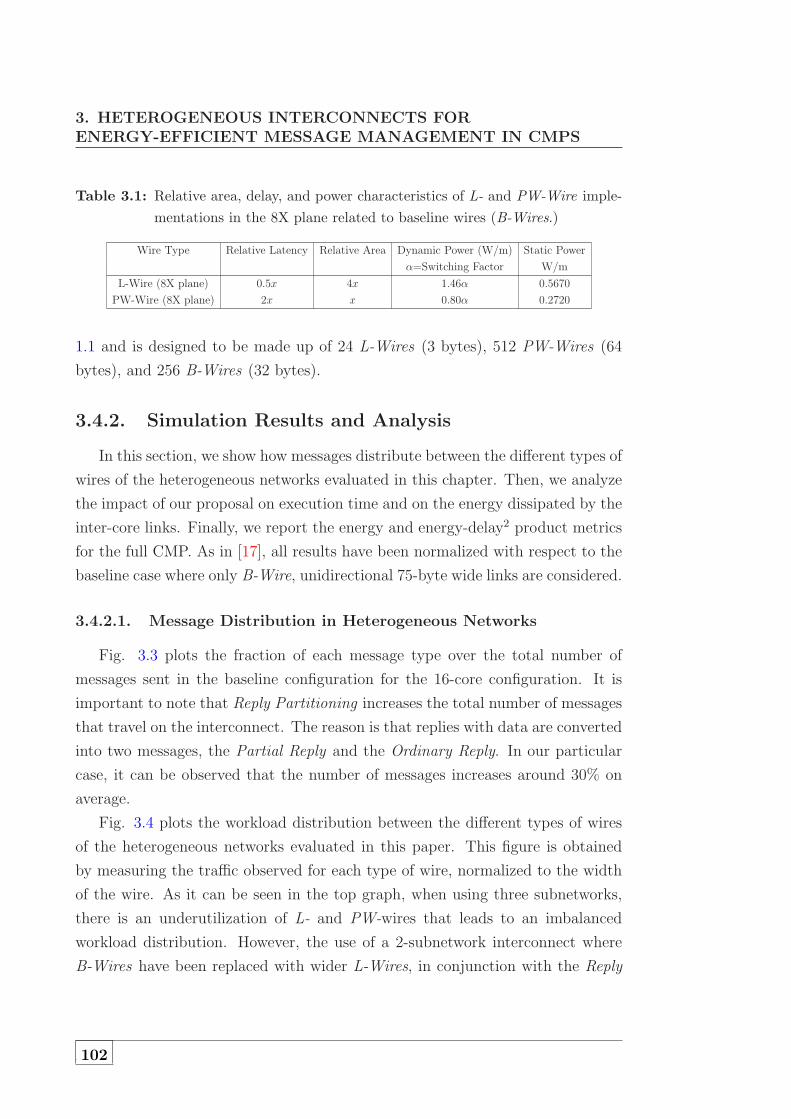
3. HETEROGENEOUS INTERCONNECTS FORENERGY-EFFICIENT MESSAGE MANAGEMENT IN CMPS
Table 3.1: Relative area, delay, and power characteristics of L- and PW-Wire imple-
mentations in the 8X plane related to baseline wires (B-Wires.)
Wire Type Relative Latency Relative Area Dynamic Power (W/m) Static Power
α=Switching Factor W/m
L-Wire (8X plane) 0.5x 4x 1.46α 0.5670
PW-Wire (8X plane) 2x x 0.80α 0.2720
1.1 and is designed to be made up of 24 L-Wires (3 bytes), 512 PW-Wires (64
bytes), and 256 B-Wires (32 bytes).
3.4.2. Simulation Results and Analysis
In this section, we show how messages distribute between the different types of
wires of the heterogeneous networks evaluated in this chapter. Then, we analyze
the impact of our proposal on execution time and on the energy dissipated by the
inter-core links. Finally, we report the energy and energy-delay2 product metrics
for the full CMP. As in [17], all results have been normalized with respect to the
baseline case where only B-Wire, unidirectional 75-byte wide links are considered.
3.4.2.1. Message Distribution in Heterogeneous Networks
Fig. 3.3 plots the fraction of each message type over the total number of
messages sent in the baseline configuration for the 16-core configuration. It is
important to note that Reply Partitioning increases the total number of messages
that travel on the interconnect. The reason is that replies with data are converted
into two messages, the Partial Reply and the Ordinary Reply. In our particular
case, it can be observed that the number of messages increases around 30% on
average.
Fig. 3.4 plots the workload distribution between the different types of wires
of the heterogeneous networks evaluated in this paper. This figure is obtained
by measuring the traffic observed for each type of wire, normalized to the width
of the wire. As it can be seen in the top graph, when using three subnetworks,
there is an underutilization of L- and PW-wires that leads to an imbalanced
workload distribution. However, the use of a 2-subnetwork interconnect where
B-Wires have been replaced with wider L-Wires, in conjunction with the Reply
102

3.4 Experimental Results
Figure 3.3: Breakdown of the messages that travel on the interconnection network
for a 16-core CMP when an L-Wire/PW-Wire heterogeneous network is
used and long critical messages are split.
Partitioning technique leads to a more balanced workload distribution (Fig. 3.4,
bottom).
3.4.2.2. Execution Time Results
Fig. 3.5 depicts the normalized execution time with respect to that obtained
for the baseline configuration for an 8- and a 16-core CMP. The first barline (C=8
or 16, Subnets=3 ) shows the normalized execution time for the 3-subnetwork
interconnect (as proposed in [17]). It can be observed an average performance
degradation of 5-13%, which is a trend also reported in [17] when a 2D torus topol-
ogy is employed. The reason of this degradation is the low use of the L-Wires
as it was shown in Fig. 3.4. Similar results are obtained when a 2-subnetwork
interconnect (L-Wire/PW-Wire) is considered without using the proposed Re-
ply Partitioning mechanism, as shown in the second barline (C=8 or 16, Sub-
nets=2 ). The reason of this performance degradation is the increased latency of
the reply messages that carry data (sent through the slower PW-Wires) which
103

3. HETEROGENEOUS INTERCONNECTS FORENERGY-EFFICIENT MESSAGE MANAGEMENT IN CMPS
Figure 3.4: Workload distribution for the 3-subnetwork approach (as in [17]) (top)
and for the 2-subnetwork approach (bottom). The use of a 2-subnetwork
interconnect in conjunction with the Reply Partitioning technique leads
to a more balanced workload distribution.
104

3.4 Experimental Results
Figure 3.5: Normalized execution time when heterogeneous links are used.
cannot be hidden by using faster L-Wires for critical messages. This degradation
has high variability, ranging from almost negligible for MP3D and Water-NSQ
applications to almost 20% for Ocean-Cont application. This result is quite
interesting because it shows that the increased latency imposed by the use of
PW-Wires for replies with data can be hidden in some applications, whilst in
others, as Barnes-Hut or Ocean-Cont, it translates into significant perfor-
mance degradation. Finally, the third barline (C=8 or 16, Subnets=2, RP) shows
the case when the proposed Reply Partitioning (RP) is applied, splitting replies
into critical, short partial replies and non-critical ordinary replies. On average,
we observe performance improvements of 16% over the two previous options for
a 16-core CMP. These important improvements are a direct consequence of the
better distribution of the messages between L-Wires and PW-Wires that Re-
ply Partitioning allows. Again, a high variability is found, with improvements
ranging from 1-2% in some applications to 50-55% in others. Compared with
the baseline configuration where no heterogeneous network is used, an average
performance improvement of 7% is obtained.
105

3. HETEROGENEOUS INTERCONNECTS FORENERGY-EFFICIENT MESSAGE MANAGEMENT IN CMPS
Figure 3.6: Normalized link energy (top) and energy-delay2 product (bottom) for the
evaluated configurations.
106

3.4 Experimental Results
Figure 3.7: Normalized energy and energy-delay2 product (ED2P ) for the full CMP.
3.4.2.3. Energy-Efficiency Results
Fig. 3.6 plots both normalized link energy and energy-delay2 product (ED2P )
metrics. The proposal developed in this work results in an average reduction
of 60%-65% in the energy dissipated by the inter-core links. This reduction is
quite similar for all applications. The ED2P metric also shows good results, with
average improvements close to 70% although, in this case, the variability between
applications is even higher because in the ED2P metric the execution time gains
importance.
Finally, Fig. 3.7 presents both the normalized energy and ED2P product
metrics for the full CMP. As it can be observed, important energy savings are
obtained for the whole CMP when applying our proposal. The magnitude of these
savings depends on the total number of cores of the CMP, ranging from 16% for
the 8-core configuration to 20% for the 16-core configuration. On the other hand,
when the ED2P metric is considered, we find an increased improvement which
ranges from 24% for the 8-core CMP to 30% for the 16-core one, due to the bigger
emphasis on the execution time.
107

3. HETEROGENEOUS INTERCONNECTS FORENERGY-EFFICIENT MESSAGE MANAGEMENT IN CMPS
3.5 Sensitivity Analysis
In this section, we discuss the impact of the issue policy of the processing
cores, link bandwidth, relative latency between the second level cache and the
interconnect, and, finally, the critical sub-block size on our proposed Reply Par-
titioning approach with a heterogeneous interconnect.
3.5.1. Out-of-order/In-order Processors
Along this chapter we have considered in-order processing cores. We have
configured Sim-PowerCMP to model a CMP with out-of-order processing cores
with the same CMP parameters described in section 2.3. Fig. 3.8 (first barline)
shows the performance speedup of our proposal over an out-of-order baseline
configuration for a 16-core CMP. All benchmarks except Ocean show degrees
of performance improvement that range from 10% for Barnes-Hut to almost
negligible for MP3D and Water-NSQ. The average reduction in the execution
time is less than what we observe in a CMP using in-order cores (an improvement
of 3% versus an 7% obtained when in-order processors were considered). This
behavior is due to the greater tolerance to long instruction latencies that an
out-of-order processor has.
3.5.2. Link Bandwidth
As we discussed before, L-Wires have a four-fold area cost compared to base-
line wires and, therefore, the number of L-Wires is quite limited. In a bandwitdth-
constrained system this constraint is exacerbated and, therefore, our proposal is
likely to not perform very well. To verify this, we consider the same base case
that authors propose in [17] where each link only has 80 B-Wires in the 8X metal
layer. As in [17], we consider twice the metal area of the new baseline intercon-
nect to implement a heterogeneous interconnect where links are designed to be
made up of 24 L-Wires (3 bytes) and 64 PW-Wires (8 bytes)3. Fig. 3.8 (second
barline) shows the performance speedup when considering narrow links respect
324 (L-Wires) ×4 + 64 (PW-Wires) = 160 (B-Wires)
108

3.5 Sensitivity Analysis
Figure 3.8: Normalized execution time when heterogeneous links and OoO cores are
used (first barline) or narrow links are considered (second barline) for a
16-core CMP.
to the new baseline interconnect. Benchmarks such as Water-SPA, Barnes-
Hut or LU, that exhibit lower network utilization or bigger available gap for
decoupling data messages into partial and ordinaries replies, show performance
improvements close to those obtained in the high-bandwidth simulations. The
rest of benchmarks suffer significant performance losses. Overall, the heteroge-
neous model performs 16% worse than the base case.
3.5.3. Relative Latency of the Interconnect with Respect
to the L2 Cache
In this section we evaluate the impact of the relative latency of the intercon-
nect with respect to the L2 cache. Fig. 3.9 shows the normalized execution time
when reply messages are split into critical, short Partial Replies and non-critical
Ordinary Replies for two L2 cache configurations: 6+2 and 10+20 cycles of access
time. For benchmarks such as Ocean, MP3D or Unstructured with either
bigger available gap or little L2 cache line utilization, Reply Partitioning per-
forms better when the weight of the interconnect over the overall L2 access time
109

3. HETEROGENEOUS INTERCONNECTS FORENERGY-EFFICIENT MESSAGE MANAGEMENT IN CMPS
Figure 3.9: Normalized execution time when heterogeneous links are used for different
L2 cache access time.
is higher (6+2 cycles configuration). On the other hand, for benchmarks that
show higher L2 cache utilizations, such as FFT, sending the full cache line using
PW-Wires has bigger impact in the execution time. This is due to the higher
weight of the interconnect in this configuration. On average, results obtained
under both configurations are quite similar because some applications perform
better under the first configuration and others under the second one.
3.5.4. Partial Reply Sub-block Size Effect
Finally, Fig. 3.10 shows the effect of augmenting the size of the cache line
sub-block carried within Partial Replies. Fig. 3.10 (top) shows the normalized
execution time with respect to that obtained for the baseline configuration for
an 8- and a 16-core CMP when Reply Partitioning technique is used along with
heterogeneous links comprised of L-Wires and PW-Wires. On average, the ob-
tained results are quite similar for sub-blocks of size 4 and 8 bytes, meanwhile the
execution time is minimized when Partial Replies carry on sub-blocks of 16 bytes
(on average, an additional 1% improvement on the normalized execution time
over the 4- and 8-byte sub-block size configuration). Fig. 3.10 (bottom) plots the
110

3.5 Sensitivity Analysis
Figure 3.10: Normalized execution time (top) and link energy (bottom) for different
size of the partial replies for 8- and 16-core CMPs.
111
3. HETEROGENEOUS INTERCONNECTS FORENERGY-EFFICIENT MESSAGE MANAGEMENT IN CMPS
normalized energy consumed by the heterogeneous links. On average, the 4-byte
sub-block size configuration consumes from 5% to 7% less energy in the inter-core
links than the 16-byte one (around 2% less when the ED2P metric is considered).
Therefore, from the point of the energy consumed in the inter-core links, the best
result is obtained for a 4-byte sub-block size for the Partial Replies.
3.6 Conclusions
In this chapter we have proposed an efficient message management mecha-
nism (from the point of view of both performance and energy) for tiled CMPs
that consists of two approaches. The first one is Reply Partitioning, a technique
that allows all messages used to ensure coherence between the L1 caches of a
CMP to be classified into two groups: critical and short, and non-critical and
long. In particular, Reply Partitioning concentrates on replies that carry data
and splits them into a critical and short Partial Reply message that carries the
word requested by the processor plus a non-critical Ordinary Reply with the full
cache block. The second approach of our proposal is the use of a heterogeneous in-
terconnection network comprised of only two different types of wires: low-latency
wires for critical messages and low-energy wires for non-critical messages which
also allows for a more balanced workload across the interconnect.
Results obtained through detailed simulations of 8- and 16-core CMPs show
that the proposed on-chip message management mechanism can reduce the power
dissipated by the links of the interconnection network about 65% with an addi-
tional reduction in execution time of 7% over previous works. Finally, these
reductions translate into overall CMP energy savings ranging from 16% for the
8-core configuration to 20% for the 16-core one (from 24% to 30% if the ED2P
metric is considered).
The sensitivity analysis show that our proposal performs better when tiles are
implemented using in-order processors (an improvement in the execution time
of 7% versus 3% obtained when out-of-order processors were considered). This
behavior is due to the greater tolerance to long load/store latencies that an out-of-
order processor has. Moreover, the relative latency between the second level cache
and the interconnect has little impact in the performance of Reply Partitioning.
112

3.6 Conclusions
Finally, when a bandwitdth-constrained system is considered, the four-fold area
cost of the L-Wires becomes a problem and, on average, the heterogeneous model
performs 16% worse than the base case.
All these results reveal that correctly organizing the interconnection network
and properly managing the different types of messages through it have significant
impact on the energy consumed by CMPs, especially for next-generation dense
CMP architectures.
113


4Exploiting Address Compression and
Heterogeneous Interconnects for Efficient
Message Management in Tiled CMPs
4.1 Introduction
As pointed out in chapter 3, one way to addres the problems that wire delay
and power dissipation will pose on future many-core CMPs is the use of hetero-
geneous on-chip interconnection networks [4], i.e., an interconnect with links that
are comprised of wires with varying physical properties [6].
Another approach, which is orthogonal to the previous one, to alleviate wire
delays and power is to transcode the transferred information in order to better
exploit the interconnect bandwidth. The area slack created due to compression
could then be exploited to further improve the latency of some particular wires.
This chapter explores such an approach by proposing the use of an address com-
pression scheme in the context of a heterogeneous interconnect that allows most
of the critical messages, used to ensure coherence between the L1 caches of a
CMP, to be compressed in a few bytes and transmitted using very low latency
wires meanwhile the rest of messages are transmitted using baseline wires. It is
important to note that we are not aimed at proposing a particular compression
scheme but at exploiting the area slack due to compression for improving critical
messages latency by means of using a heterogeneous interconnect.
115

4. EXPLOITING ADDRESS COMPRESSION ANDHETEROGENEOUS INTERCONNECTS FOR EFFICIENTMESSAGE MANAGEMENT IN TILED CMPS
The rest of the chapter is organized as follows. Section 4.2 reviews some
related work. Section 4.3 gives a overview to some traditional address compression
schemes. Our proposal for optimizing the on-chip interconnection network energy
and performance in tiled CMPs is presented in section 4.4. Section 4.5 presents
the results of the proposed mechanism. A sensitivity analysis is presented in
section 4.6. Finally, section 4.7 summarizes the main conclusions of the chapter.
4.2 Related Work
Several address compression schemes have been proposed to reduce their en-
ergy and/or area cost. Address compression schemes based on using a small
compression cache were first proposed in [25] and were used to reduce off-chip
bus widths and pin count. Recent attempts at using compression to reduce on-
chip wire delay and/or energy consumption have been presented in the last years.
In [19], Criton proposes to exploit low entropy in order to reduce wire delay. How-
ever, in that work, performance results are based on estimations instead of using
simulations. Liu et al. [60] propose an evolution of the mechanism described in
[25]. They describe a partial match compression (PMC) scheme for the address
bus between the L1 and L2 caches in a single-core processor executing sequential
applications in order to reduce wire delay by increasing inter-wire spacing. Per-
formance improvement of up to 16% is obtained for some configurations, however,
they do not estimate the effect of their proposal on energy consumption.
Basu et al. [7] propose placing a value cache at both ends of a communication
channel. Upon a hit, the system sends the index to the cache entry instead of
the whole word, to reduce bit transitions. Parcerisa and Gonzalez [73] applied
value prediction to inter-cluster communication on clustered microarchitectures
in order to reduce long wire delays. In [59], the authors propose a communication
value cache (CVC) to reduce the number of bit transfers between processors inside
a bus-based CMP architecture. Differently from previous works, we show how ad-
dress compression could be used in conjunction with a heterogeneous network to
improve performance and reduce energy consumption in tiled CMP architectures.
In addition to address compression schemes, some authors have recently pro-
posed to compress NoC traffic through exploiting frequent data patterns/values.
116

4.3 Address Compression Schemes
In [23], the authors discovered that some patterns occur with very high frequen-
cies in on-chip traffic. They then propose to take advantage of this observation
by using a cache compression mechanism that allows to increase the effective
cache capacity along with network compression in order to reduce network la-
tency with additional power savings. P. Zhou et al. propose to exploit frequent
values instead of value patterns [101], using a very small table for end-to-end
communications where frequent values are stored. When sending a data mes-
sage, values are compared with the values stored in that table and on a hit the
index of the table is sent. Otherwise the original value is used. In this way, they
obtain average reductions of 24% in the data message length with reductions of
up to 16.7% in the router power. In [44], it is proposed a similar data compression
scheme where indexes are stored in a shared table instead of per flow basis. And
additional management protocol ensures that in-order delivery is not required.
Both proposals can be applied simultaneously with our proposal of using a het-
erogeneous interconnection network comprised of a small set of very-low-latency
wires (VL-Wires) for critical short-messages in addition to baseline wires. But,
with average reductions of 24% in the length of data message [101], the use of
VL-Wires for compressed data messages has to be discarded because of the very
limited number of wires of this type.
4.3 Address Compression Schemes
As mentioned before, address buses have been widely studied in the literature
and several strategies have been adopted in order to eliminate redundant and/or
useless information. Dynamic compression schemes were first proposed by Farrens
et al. [25]. Their Dynamic Base Register Caching (DBRC) scheme consists of
a small compression cache at the sending end, and register files at the receiving
end of a processor-memory address bus. When a hit happens in the sender
compression cache, the system sends the index to the cache entry instead of the
whole address, thus reducing the number of wires needed to implement the address
bus. In [60] the authors present Partial Match Compression Scheme (PMCS) that
exploits the spatial and temporal locality of addresses to dynamically compress
them depending on the extent to which they match the higher-order portions
117

4. EXPLOITING ADDRESS COMPRESSION ANDHETEROGENEOUS INTERCONNECTS FOR EFFICIENTMESSAGE MANAGEMENT IN TILED CMPS
CH C1 C0
CH
CH
Tmiss
Tmiss
Tmiss
CH
CH
CH I U
CH I U
C1 C0
C0C1
Tmiss
Control Bits
1
0 0 0
0 0 1
0 1 0
0 1 1
PM complete hit
DBRC hit
PM partial hit
DBRC miss
DBRC miss
PM Complete miss
I
I
U
U
Partition 4 (complete miss)
Partition 3Partition 2
Partition 1
Partition 4 (complete hit)
T
T I U
I U
Figure 4.1: Partial Match Address Compression Scheme (source: [60]).
of recently-occurring addresses saved in a small compression cache. When a
maximal match occurs, the address is compressed to the maximum extent and is
transmitted on a narrow bus in one cycle. When a partial match occurs, one or
more extra cycles are required. Fig. 4.1 shows PMCS when three candidates for
partial match are considered. For a complete hit/miss the behavior is the same
than in DBRC, but when a partial hit happens, the additional bits codify which
low-order portion (Tmiss) is sent through the bus.
Fig. 4.2 (left) shows how to adapt the DBRC scheme to a tiled CMP archi-
tecture in which the global bus is replaced by a switched direct network (similar
adaption can be done for the PMCS). An alternative compression scheme is shown
in Fig. 4.2 (right). In this case, the compression cache at the sending end is re-
placed with a base register that stores the last non-compressed address sent by
the source core to that destination. At the receiving end, a similar base register
also stores that address. When the difference between the address stored at the
sending end and a subsequent address can be represented using less than a fixed
number of bits, the system sends just the difference instead of the whole address,
updating the information stored in the base register in both the sending and the
receiving cores. This simple scheme is based on the fact that many memory ref-
118

4.3 Address Compression Schemes
Address from L1 Cache Core
Address to Directory Slice
Link
Address from L1 Cache Core
+
Address to Directory Slice
CoreSending
CoreReceiving
Index
IndexTypeDestSrc
BaseRegister
Array
Higher Order Bits
Higher Order Bits
TypeDestSrc Difference
Difference
Higher Order Bits
Higher Order Bits
BaseRegister
Cache
BaseRegister
BaseRegister
Lower Order Bits
Lower Order Bits
Lower Order Bits Lower Order Bits
Lower Order Bits
Figure 4.2: Organization of the DBRC (left) and Stride (right) address compression
schemes for tiled CMP architectures.
erences, beyond affine access functions, can be easily predicted as they follow a
stride pattern [78].
In order to guarantee a proper synchronization of address values in both ends
of the communication channel when using a switched direct network, all theses
hardware structures are maintained per a flow [101]. Although it might be pos-
sible to use a shared table scheme as in [44], the complexity of synchronization
may offset the benefits in area savings. For a 16-core processor the overall area
overhead is less than 5% of the area needed for a core (see Table 4.1).
We have evaluated the effectiveness of the compression schemes described
before in the context of a tiled CMP running parallel applications. Fig. 4.3 shows
the fraction of compressed addresses using different configurations for the DBRC
and Stride compression schemes (see section 4.5 for further details about the 16-
core CMP configuration and working sets evaluated). Results for PMCS are not
presented because its compression coverage is similar to the simpler and more
cost-effective DBRC scheme. Some interesting results can be pointed out. First,
if we try to keep address compression size to one byte, a low compression coverage
is obtained for both the Stride compression scheme, and the DBRC scheme when
a small compression cache is considered (1-byte Stride and 4-entry DBRC (1B
LO) bars). In order to obtain acceptable compression coverages (over 80%), we
need either to implement a compression cache with, at least, 16 entries (16-entry
119

4. EXPLOITING ADDRESS COMPRESSION ANDHETEROGENEOUS INTERCONNECTS FOR EFFICIENTMESSAGE MANAGEMENT IN TILED CMPS
Figure 4.3: Address compression coverage for a 16-core tiled CMP.
DBRC (1B LO) bar); or to use an address compression size of two bytes (2-byte
Stride or 4-entry DBRC (2B LO) bars). In the last case, the Stride compression
scheme obtains similar results to an equivalent DBRC configuration eliminating
the need of using an adder. These results show that, in this case, compression
schemes based on the use of stride patterns perform badly in comparison with
other proposals. Finally, DBRC with a compression size of 2 bytes shows average
address compression coverages of around 98%. These results show that traditional
compression schemes provide significant coverage that can be exploited.
It is important to note that we are not aimed at proposing a particular com-
pression scheme but at exploiting the area slack due to compression for improving
critical messages latency and ensuring efficient message management in CMPs by
means of using a heterogeneous interconnect.
In order to evaluate the hardware cost of the address compression schemes for
a tiled CMP architecture, Table 4.1 shows the area and power characteristics of
different configurations for these two address compression schemes along with the
percentage relative to one of the cores of the CMP. The measurements have been
carried out using CACTI v4.1 [87] for a 65 nm process technology. In each core,
120

4.4 Combining Address Compression and Heterogeneous Networks
Table 4.1: Area and power characteristics of different address compression schemes
for a 16-core tiled CMP. For comparison purposes, in parenthesis we show
the area and power relative to one of the cores of the CMP.
Compression Scheme Size (Bytes) Area (mm2) Max. Dyn. Power (W) Static Power (mW)
4-entry DBRC 1088 0.0723 (0.29%) 0.1065 (0.48%) 10.78 (0.29%)
16-entry DBRC 4352 0.2678 (1.07%) 0.3848 (1.72%) 43.03 (1.21%)
64-entry DBRC 17408 0.8240 (3.30%) 0.7078 (3.16%) 133.42 (3.76%)
2-byte Stride 272 0.0257 (0.1%) 0.0561 (0.25%) 5.14 (0.15%)
we need to implement one sending structure and as many receiving structures
as the number of cores. Moreover, requests and coherence commands use their
own hardware structures to avoid destructive interferences between both address
streams. It can be seen that the relative cost of implementing these compression
schemes with respect to a core ranges from 0.1-0.25% for the 2-byte Stride scheme
to 3.3-3.7% for the 64-entry DBRC one.
4.4 Combining Address Compression and Heteroge-
neous Networks
In this section we present our proposal for combining address compression
and heterogeneous networks for reduced energy consumption in tiled CMPs. As
introduced before, there are two main components in our proposal. The first is
the use of an address compression scheme that allows for a significant area slack.
The second is the use of a heterogeneous interconnect that exploits that area
slack for wire latency improvement by using two different set of wires. Messages
are sent through the appropriate set, according to their latency and bandwidth
requirements.
As we saw in chapter 3, messages involved in the L1 cache coherence protocol
can be classified according to their criticality into critical and non-critical mes-
sages. We say that a message is critical when it is in the critical path of the L1
cache miss. In other case, we call the message as non-critical. On the other hand,
coherence messages can also be classified according to their size into short and
121

4. EXPLOITING ADDRESS COMPRESSION ANDHETEROGENEOUS INTERCONNECTS FOR EFFICIENTMESSAGE MANAGEMENT IN TILED CMPS
long messages. Coherence responses do not include the address or the data block
and just contain control information (source/destination, message type, MSHR
id, etc). Therefore, they are classified as short messages. Other message types, in
particular requests, responses without data and coherence commands, also con-
tain address block information but they are still narrow enough to be classified
as short messages. They are the focus of our proposal. Finally, replacements
with data and data block transfers also carry a cache line and, therefore, they
are classified as long messages. It is important to remember that, as pointed out
in chapter 2, more than 50% of the messages travelling on the on-chip intercon-
nection network for a 16-core CMP configuration running the applications used
in our evaluation are short messages containing address block information that
can be compressed.
4.4.1. Interconnect Design for Efficient Message Manage-
ment
As discussed in the previous chapter, L-Wires have a four-fold area cost com-
pared to baseline wires and, therefore, the number of L-Wires is quite limited.
Considering that they will be used for sending short, critical messages, previous
proposals have fixed their amount according to the typical size of short messages
(e.g., 11 bytes). The remaining area have been employed for sending long mes-
sages. However, by using an address compression scheme the amount of L-Wires
can be reduced dramatically, from 11 bytes to 4-5 bytes depending on the size
of the uncompressed low order bits used by the underlying compression scheme,
which arises an area slack than can be exploited for further improving wire la-
tency, i.e., having thicker but faster wires. We denote this new kind of wires as
VL-Wires (very-low-latency wires).
Table 4.2 shows the relative delay, area, and power characteristics of the new
VL-Wires for different wire widths compared to baseline wires (B-Wires) when a
single metal plane is considered (8X plane). In order to match the metal area of
the baseline configuration, in our proposal, each original 75-byte unidirectional
link is designed to be made up of 24 to 40 VL-Wires (3 to 5 bytes) with different
relative latencies and area cost, as shown in Table 4.2, and 272 B-Wires (34
122

4.5 Experimental Results
Table 4.2: Relative delay, area, and power characteristics of VL-Wires (8X plane)
related to baseline wires (B-Wires) for different widths.
Wire Width Relative Latency Relative Area Dynamic Power (W/m) Static Power
α=Switching Factor W/m
3 Bytes 0.27x 14x 0.87α 0.3065
4 Bytes 0.31x 10x 1.00α 0.3910
5 Bytes 0.35x 8x 1.13α 0.4395
bytes)1. Therefore, in our proposed heterogeneous interconnect VL-Wires will be
used for sending already short, critical messages (e.g., coherence replies) as well
as compressed requests and compressed coherence commands. Uncompressed and
long messages will be sent through the original B-Wires.
4.5 Experimental Results
This section shows the results that are obtained for our proposal under differ-
ent scenarios and compares them against those achieved with the configuration
that employs just B-Wires, which is taken as baseline. For comparison purposes,
we also show the behavior assuming perfect address compression, which is repre-
sented in the figures using lines instead of barlines.
4.5.1. Simulation Results and Analysis
In this section we analyze, first, the impact of our proposal on the execution
time and on the energy-delay2 product metric for the inter-core links. Then,
we evaluate the energy-delay2 product metric for the full CMP. All results have
been normalized with respect to the baseline configuration where only B-Wire,
unidirectional 75-byte wide links are considered and they include the additional
1Note that the heterogeneous interconnect (VL-Wires+B-Wires) always matches the metal
area of the baseline interconnect (75-Byte or 600 B-Wires). E.g., for 3-byte VL-Wires the
distribution is: 24 (VL-Wires) × 14 + 272 (B-Wires) ≃ 608 (B-Wires). For 5-byte VL-Wires :
40 (VL-Wires) × 8 + 272 (B-Wires) ≃ 592 (B-Wires).
123

4. EXPLOITING ADDRESS COMPRESSION ANDHETEROGENEOUS INTERCONNECTS FOR EFFICIENTMESSAGE MANAGEMENT IN TILED CMPS
cost due to the extra hardware structures needed to implement the different
address compression schemes evaluated.
Fig. 4.4 (top) depicts the normalized execution time with respect to that
obtained for the baseline configuration for a 16-core CMP. Barlines show the
normalized execution time for several Stride and DBRC address compression
schemes, in particular those with a compression coverage over 80% as reported
in Fig. 4.3. The number of bytes used to send the low order bits (1 or 2 bytes)
determines the number of VL-Wires in the heterogeneous network (4 or 5 bytes).
For comparison purposes, and in order to show the potential improvement in
the execution time, three additional solid lines have been added to show the
execution time for the different heterogeneous network configurations when a
perfect compression coverage (100%) is considered. It can be observed that a
4-entry DBRC compression scheme with 2 low-order bytes is enough to achieve
an average performance improvement of 8% (close to 10% of maximum potential
performance improvement). This improvement has high variability, ranging from
almost 1-2% for Water and LU to 22-25% for MP3D and Unstructured.
This variability is due to two factors. First, some applications, as Water or LU,
present low intercore data sharing patterns [96]. In these cases, the coherence
traffic is small and our proposal has little impact in the execution time. Other
applications, such as MP3D or Unstructured, present better traffic patterns
and can take advantage of a faster interconnect. The second factor that explains
this variability is related with the address compression scheme coverage. As it
was shown in Fig. 4.3, applications such as Barnes-Hut or Radix exhibit low
address compression coverage for most of the configurations proposed. For these
applications, the reduction in the execution time does not match the maximum
potential even when a 64-entry configuration is used.
Fig. 4.4 (bottom) plots the normalized energy-delay2 product (ED2P ) metric.
Average reductions close to 40% are obtained, although again, a high variability
among applications is observed. Some applications, such as Water and LU,
show reductions of around 20% due mainly to the lower power dissipation of
the proposed heterogeneous interconnection network; others, such as MP3D and
Unstructured, present a reduction of 65% in the ED2P metric due to bigger
emphasis on the execution time that the ED2P metric does.
124

4.5 Experimental Results
Figure 4.4: Normalized execution time (top) and link ED2P metric (bottom) for dif-
ferent address compression schemes over heterogeneous links (VL-Wires
width matches address compression size).
125

4. EXPLOITING ADDRESS COMPRESSION ANDHETEROGENEOUS INTERCONNECTS FOR EFFICIENTMESSAGE MANAGEMENT IN TILED CMPS
Figure 4.5: Normalized execution time (top) and ED2P metric (bottom) for different
address compression schemes over heterogeneous links with fixed 3-byte
VL-Wires width and message fragmentation.
126

4.5 Experimental Results
Figure 4.6: Normalized energy-delay2 product (ED2P ) for the full CMP (3-byte VL-
Wires configuration).
On the other hand, Fig. 4.5 shows the normalized execution time (top) and
ED2P metric (bottom) when the number of VL-Wires is restricted to 3 bytes, the
minimum size of the messages flowing through the interconnect, independently
of the address compression scheme used. In this case, the compressed messages
are sent through VL-Wires using fragmentation when needed. This configuration
allows for a minimum latency for responses without data and coherence responses
(3-byte long) with little penalty for compressed messages (4- or 5-byte long). In
this case, an additional reduction in both execution time and the ED2P metric
is obtained. For the 4-entry DBRC compression scheme with 2 low-order bytes,
an average performance improvement of 10% is obtained (two additional points
with respect to the results obtained when VL-Wires width is designed depending
on the address compression size). When the ED2P metric is considered, average
reductions over 35% are obtained for the 4-entry DBRC compression scheme going
up to 38% for the 64-entry configuration.
Finally, Fig. 4.6 presents the normalized ED2P metric for the full CMP
assuming the 3-byte VL-Wires configuration. Average improvements range from
23% for the 2-byte Stride configuration to 28% for the 4-entry DBRC one. As it
can be observed, when the number of entries of the DBRC compression scheme is
127

4. EXPLOITING ADDRESS COMPRESSION ANDHETEROGENEOUS INTERCONNECTS FOR EFFICIENTMESSAGE MANAGEMENT IN TILED CMPS
increased, worse ED2P metrics are obtained for the full CMP. This is due to the
bigger impact that the extra hardware structures have, which is not compensated
with a significant reduction in the execution time.
4.6 Sensitivity Analysis
In this section, we discuss the impact of using out-of-order processors cores,
link bandwidth and relative latency between the second level cache and the in-
terconnect on our proposed address compression technique with a heterogeneous
interconnect.
4.6.1. Out-of-order/In-order Processors
Along this chapter we have considered in-order processing cores. In this sec-
tion we evaluate the effect of using out-of-order (OoO) cores in order to show how
even with this kind of cores, which allow for potential overlapping of several cache
misses, our proposal still shows important performance improvements. Note that
the use of OoO cores in future many-core CMP designs seems unlikely due to the
increased area and energy consumption that this kind of processor cores would
entail.
We have configured Sim-PowerCMP to model a CMP with OoO cores. Non-
blocking first level caches have been considered, which allows overlapping some
cache misses, and a ROB with 64 entries is used. Fig. 4.7 shows the performance
speedup of our proposal over an out-of-order baseline configuration for a 16-
core CMP. All benchmarks except Ocean-Cont show degrees of performance
improvement that range from 25-27% for MP3D and Unstructured to almost
negligible for Water-NSQ. Although still noticable, the average reduction in
the execution time is lower than what we observe in a CMP using in-order cores
(an improvement of 7% versus a 9% when in-order cores were considered). This
behavior is due to the greater tolerance to long instruction latencies that an
out-of-order processor allows for.
128

4.6 Sensitivity Analysis
Figure 4.7: Normalized execution time for different address compression schemes over
heterogeneous links when OoO cores are used for a 16-core CMP.
4.6.2. Link Bandwidth
As discussed previously, the number of VL-Wires is quite limited. In a
bandwidth-constrained system this restriction is exacerbated and, therefore, our
proposal is likely not to perform very well. To verify this, we consider the same
base case that Cheng et al. propose in [17] where every link has only 80 B-
Wires at the 8X- metal layer. As in [17], we consider twice the metal area of
the new baseline interconnect to implement a heterogeneous interconnect where
links are designed to be made up of 24 L-Wires (3 bytes) instead of using any
faster and thicker VL-Wires and 64 PW-Wires (8 bytes)2. Fig. 4.8 shows the
performance speedup for narrow links over the new baseline interconnect. Bench-
marks such as Water, Barnes-Hut, Unstructured or LU that exhibit lower
network utilizations still show marginal performance improvements. The rest of
the benchmarks suffer significant performance losses. Overall, the heterogeneous
model performed 15% worse than the base case.
224 (L-Wires) × 4 + 64 (B-Wires) 0 80 × 2 (B-Wires).
129

4. EXPLOITING ADDRESS COMPRESSION ANDHETEROGENEOUS INTERCONNECTS FOR EFFICIENTMESSAGE MANAGEMENT IN TILED CMPS
Figure 4.8: Normalized execution time for different address compression schemes over
heterogeneous links when narrower and slower L-Wires (instead of VL-
Wires) are considered for a 16-core CMP.
4.6.3. Relative Latency of the Interconnect with Respect
to the L2 Cache
In this section we evaluate the impact of the relative latency of the intercon-
nect with respect to the L2 cache. Fig. 4.9 shows the normalized execution time
when different compression schemes are used in conjunction with heterogeneous
links for two L2 cache access time configurations: 6+2 and 10+20 cycles of access
time. On average, our proposal performs 3% better when a more up-to-date ac-
cess time is considered (6+2 cycles configuration). An improvement of 6% versus
9% is obtained when L2 caches slices that present higher latencies (10+20 cycles)
are considered.
For most of the applications the use of L2 caches with higher latencies has
little impact on the performance (performance improvement is 0-2% worse than
the one obtained with the initial cache configuration). For some applications for
which the execution time is highly dependent on the memory hierarchy laten-
cies (with increases in execution time that range from 10-15% for Raytrace
or Unstructured to almost 30% for MP3D), our proposal suffers significant
130
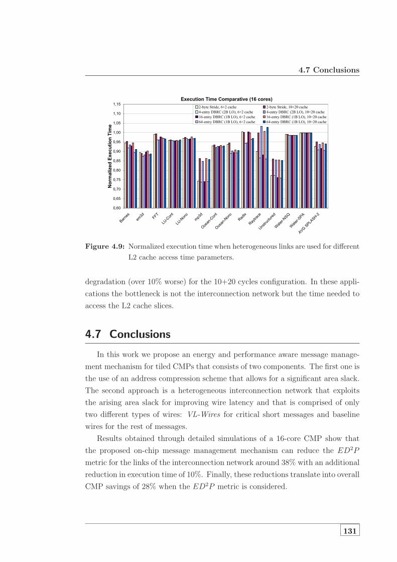
4.7 Conclusions
Figure 4.9: Normalized execution time when heterogeneous links are used for different
L2 cache access time parameters.
degradation (over 10% worse) for the 10+20 cycles configuration. In these appli-
cations the bottleneck is not the interconnection network but the time needed to
access the L2 cache slices.
4.7 Conclusions
In this work we propose an energy and performance aware message manage-
ment mechanism for tiled CMPs that consists of two components. The first one is
the use of an address compression scheme that allows for a significant area slack.
The second approach is a heterogeneous interconnection network that exploits
the arising area slack for improving wire latency and that is comprised of only
two different types of wires: VL-Wires for critical short messages and baseline
wires for the rest of messages.
Results obtained through detailed simulations of a 16-core CMP show that
the proposed on-chip message management mechanism can reduce the ED2P
metric for the links of the interconnection network around 38% with an additional
reduction in execution time of 10%. Finally, these reductions translate into overall
CMP savings of 28% when the ED2P metric is considered.
131

4. EXPLOITING ADDRESS COMPRESSION ANDHETEROGENEOUS INTERCONNECTS FOR EFFICIENTMESSAGE MANAGEMENT IN TILED CMPS
The sensitivity analysis shows that our proposal performs better when tiles are
implemented using in-order processors (an improvement in the execution time of
7% versus a 9% is obtained when out-of-order processors were considered). This
behavior is due to the greater tolerance to long load/store latencies that an out-
of-order processor has. Moreover, the relative latency between the second level
cache and the interconnect has little impact on the performance of our proposal
(an improvement of 6% versus a 9%). Finally, when a bandwidth-constrained
system is considered, the four-fold area cost of the L-Wires becomes a problem
and, on average, the heterogeneous model performs 15% worse than the base case.
132
5Energy-Efficient Hardware Prefetching
for CMPs using Heterogeneous
Interconnects
5.1 Introduction
One way to tackle problems due to wire delay is to use latency hiding tech-
niques like hardware prefetching, which eliminates some cache misses and/or
overlaps the latencies of others. Unfortunately, hardware prefetching significantly
increases on-chip communication since coherence between the L1 caches of the
tiled CMP must be ensured, increasing the power consumption of the on-chip
interconnect. As an example of the latter, Fig. 5.1 shows, for three hardware
prefetching alternatives (see section 5.3 for further details), the average improve-
ment in terms of execution time and the increase in the on-chip network power
consumption due to the extra communication that prefetching entails for the par-
allel scientific applications considered across this Thesis. As it can be observed,
increases over 20% in the on-chip network power consumption are obtained for
some of the prefetching techniques considered in this chapter.
Another already commented approach to alleviate the negative effect of wire
delays and the increasing interconnect power consumption is the use of heteroge-
neous on-chip interconnection networks [4], i.e., an interconnect with links com-
prised of wires with varying physical properties.
133

5. ENERGY-EFFICIENT HARDWARE PREFETCHING FORCMPS USING HETEROGENEOUS INTERCONNECTS
Figure 5.1: Normalized execution time and network power consumption for a 16-core
CMP when different prefetching techniques are considered.
In this chapter we explore such an approach by proposing the use of a het-
erogeneous interconnect in the context of hardware prefetching schemes for tiled
CMPs. In this way, we can improve the energy-efficiency of prefetching techniques
by transmitting prefetched lines through low-power wires meanwhile the rest of
the messages are transmitted using baseline wires. It is important to note that
we are not aimed at proposing a particular prefetching scheme but at exploiting
the non-critical nature of these messages by means of using the energy-efficient
and slower wires of a heterogeneous interconnect.
The rest of the chapter is organized as follows. Section 5.2 reviews some re-
lated work. Section 5.3 presents a background on hardware prefetching. Our
proposal for optimizing the on-chip interconnection network energy and perfor-
mance in tiled CMPs is presented in section 5.4. Section 5.5 presents the results
of the proposed mechanism. A sensitivity analysis is presented in section 5.6.
Finally, section 5.7 summarizes the main conclusions of the chapter.
134

5.2 Related Work
5.2 Related Work
Hardware prefetching has been proposed and explored by many researchers
[16; 46; 77], and is currently implemented in many existing systems [39; 82]. From
mid-sixties, early studies [2] of cache design recognized the benefits of prefetch-
ing. Hardware prefetching of separate cache blocks was later implemented in
the IBM 370/168 and Amdahl 470V [83]. Smith summarizes several of these
early approaches in his survey of cache memories [84]. Jouppi [47] introduced
stream buffers that trigger successive cache line prefetches on a miss. Chen and
Baer [16] proposed variations of stride-based hardware prefetching to reduce the
cache-to-memory latency. Dahlgren et. al. [22] proposed an adaptive sequential
(unit-stride) prefetching scheme that adapts to the effectiveness of prefetching.
Ki and Knowles [50] used extra cache bits to increase the accuracy of prefetching.
Srinivasan et. al. [86], classified prefetches according to whether they reduce or
increase misses or traffic.
5.3 Hardware Prefetching
In this section we present a general background on hardware prefetching fo-
cusing on the schemes that we have chosen to evaluate our proposal. A more
exhaustive study about data prefetching can be found in [90].
The simplest hardware prefetching schemes are variations upon the one block
lookahead (OBL) approach which initiates a prefetch for block b+ 1 when block
b is accessed. Smith [84] summarizes several of these approaches of which the
prefetch-on-miss (OnMiss) and tagged prefetch algorithms (Tagged) will be dis-
cussed here. The prefetch-on-miss algorithm simply initiates a prefetch for block
b+ 1 whenever an access for block b results in a cache miss. The tagged prefetch
algorithm associates a tag bit with every memory block. This bit is used to detect
when a block is demand-fetched or a prefetched block is referenced for the first
time. In either of these cases, the next sequential block is fetched. In order to
avoid memory stalls suffered by processors, it is possible to increase the number
of blocks prefetched after a demand fetch from one to K, where K is known as
the degree of prefetching.
135
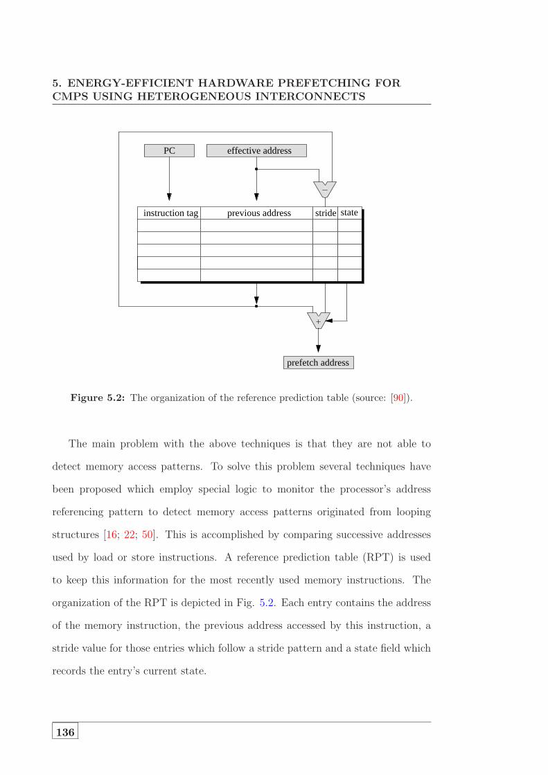
5. ENERGY-EFFICIENT HARDWARE PREFETCHING FORCMPS USING HETEROGENEOUS INTERCONNECTS
instruction tag previous address stride state
PC effective address
prefetch address
Figure 5.2: The organization of the reference prediction table (source: [90]).
The main problem with the above techniques is that they are not able to
detect memory access patterns. To solve this problem several techniques have
been proposed which employ special logic to monitor the processor’s address
referencing pattern to detect memory access patterns originated from looping
structures [16; 22; 50]. This is accomplished by comparing successive addresses
used by load or store instructions. A reference prediction table (RPT) is used
to keep this information for the most recently used memory instructions. The
organization of the RPT is depicted in Fig. 5.2. Each entry contains the address
of the memory instruction, the previous address accessed by this instruction, a
stride value for those entries which follow a stride pattern and a state field which
records the entry’s current state.
136

5.4 A Proposal for Energy-Efficient Prefetching Management in TiledCMPs
5.4 A Proposal for Energy-Efficient Prefetching Man-
agement in Tiled CMPs
In this section we present our proposal for reducing the energy dissipated by
prefetching techniques in tiled CMPs. This section starts with a classification
of the messages in terms of both their criticality and size when prefetching is
employed and finishes with the description of the proposed mechanism.
5.4.1. Classification of Messages in Tiled CMP Architec-
tures with Prefetching
In order to take into account prefetching in the classification of the different
kind of messages traveling on the interconnect introduced in section 2.6.1, we
need to change the definition of Request messages as follows: messages that are
generated by cache controllers in response to L1 cache misses, or a likely future L1
cache miss when prefetching is considered, and sent to the corresponding home
L2 cache to demand privileges over a memory line. The rest of definitions remain
unchanged.
Using the criticality criterion introduced in section 2.6.1, all messages related
with prefeching can be considered as non-critical because they deal with data
blocks that will be needed in the future. It is clear that slight slowdowns in the
delivery of non-critical messages will not cause any performance degradation and
that energy is saved when this kind of messages travel on slower, power-efficient
PW-Wires. They will be the focus of our proposal.
Fig. 5.3 (top) plots the fraction of each message type over the total number of
messages for a 16-core CMP configuration when different prefetching mechanisms
are considered and for the applications used in our evaluation (see section 5.5 for
evaluation details). We have focused on the applications for which hardware
prefetching is useful, so some applications such as LU-Nonc, Radix or Water-
SPA are not considered. Results have been normalized with respect to a base
configuration without prefetching. As pointed out before, hardware prefetching
significantly increases on-chip communication. Average increases of about 20% in
network traffic are observed. And, on average, between 16% to 34% of the network
137

5. ENERGY-EFFICIENT HARDWARE PREFETCHING FORCMPS USING HETEROGENEOUS INTERCONNECTS
Figure 5.3: Breakdown of the messages that travel on the interconnection network
for a 16-core CMP (top) and percentage of the power consummed in the
interconnect by each type of message (bottom).
138

5.4 A Proposal for Energy-Efficient Prefetching Management in TiledCMPs
traffic is due to prefetching (prefetch requests, their corresponding replies and all
coherence traffic involved), whereas the rest has to do with ordinary messages.
Even more interesting is Fig. 5.3 (bottom) which shows a breakdown of the
network power consumption for each message type. Again, results are normalized
with respect to the network power consumption when no prefetching technique
is used. The amount of power consumed in the interconnect associated with
prefetching traffic ranges from 17-18% when the more complex stride prefetching
is used, to 32-40% for the simplest schemes.
As previously commented, most of this power is consumed in the point-to-
point links, and therefore, message size plays a major role. In particular, prefetch
replies are 67-byte long since they carry control information (3-bytes) and a cache
line (64 bytes). On the contrary, requests and coherence commands are 11-byte
long since beside control information (3 bytes) they also carry address information
(8 bytes). Finally, coherence replies are just 3-byte long. Therefore, optimizing
the delivery of the prefetch replies that carry data will be rewarding to reduce
the energy dissipated by the interconnection network in CMPs.
5.4.2. Interconnect Design for Efficient Message Manage-
ment
As discussed in section 1.1, PW-Wires have the same area cost than baseline
wires while they are twice slower. Fixing the number of PW-Wires is not a naive
task. They will be used for sending prefeching-related messages (in particular,
prefetch replies with data), whereas the remaining area will be consumed by B-
Wires employed for sending ordinary messages and short (11-byte and 3-byte
long) prefeching-related messages. The proportion between PW- and B-Wires
has direct impact on both the execution time and the power consumption of
the interconnect. Preliminary simulations with different proportions of PW- and
B-Wires showed that the best option is to replace half of the original wires by
PW-Wires.
In order to match the metal area of the baseline configuration, in our heteroge-
neous interconnect design, each original 75-byte unidirectional link (600 B-Wires)
139

5. ENERGY-EFFICIENT HARDWARE PREFETCHING FORCMPS USING HETEROGENEOUS INTERCONNECTS
Figure 5.4: Normalized execution time for different prefetching schemes (with and
without heterogeneous links) for a 16-core CMP.
is now designed to be made up of 296 B-Wires (37 bytes) and 304 PW-Wires (38
bytes).
5.5 Simulation Results and Analysis
In this section we analyze the impact of our proposal on both the execution
time and the power consumption for the inter-core links. All results have been
normalized with respect to the baseline non-prefetching configuration where only
B-Wire, unidirectional 75-byte wide links are considered (with the exception of
Fig. 5.6 where results are normalized with respect to a 16-core CMP with the
same prefetching technique).
Fig. 5.4 shows the normalized execution times with respect to those obtained
for the baseline configuration for a 16-core CMP without prefetching. In par-
ticular, barlines show the normalized execution times for the prefetch-on-miss
(OnMiss), tagged prefetch (Tagged), and stride-based prefetch (Stride) tech-
niques (see section 5.3) applied to the L1D private caches. The stride-based
prefetching is based on the implementation of the IBM Power 4 [89]. Each
140

5.5 Simulation Results and Analysis
prefetcher contains three separate filter tables: positive unit stride, negative unit
stride, and non-unit stride. Once a filter table entry detects a miss stream, the
prefetcher allocates an entry in the stream table and initiates the prefetch of
K consecutive cache blocks (for the OnMiss and Tagged prefetching schemes
the value of K is set to 1). For comparison purposes, the normalized execu-
tion time obtained when only B-Wires are employed is also shown. On average,
we obtain improvements in execution time of around 10% for all the prefetch-
ing techniques evaluated, which demonstrates the convenience of using hardware
prefetching in future many-core CMPs. This improvement has high variability,
ranging from almost negligible or even a slight degradation for Barnes-Hut,
Raytrace, Unstructured andWater to improvements of 20-35% for EM3D
and Ocean-Cont.
This observed variability is due to the memory access patterns exhibited by the
applications. Some applications, as FFT, LU-Cont, or Ocean-Cont, present
regular memory access patterns that lead to high percentage of useful prefetches
as we can see in Fig. 5.5 (top) where we present a classification of the prefetches.
In this figure, prefetches are classified into: useful if the prefetched line is accessed
before being replaced, late if other requests coalesce into the MSHR allocated for
the prefetched line, useless if the prefetched line gets replaced before it is re-
quested by the processor, unnecesary if the prefetch coalesces into a MSHR for
an already-on-the-fly cache miss, and invalidated if the prefetched line gets inval-
idated before being requested by the processor. On the other hand, applications
such as Barnes-Hut or Raytrace show a high percentage of late or useless
prefetches that lead to negligible improvements in the execution time.
Going back to Fig. 5.4, when heterogeneous links are considered, an average
slowdown of about 2% is observed with respect to the B-Wire-only configuration
that also uses prefetching. In this case, similar degradations are obtained for all
the applications. This degradation is explained by the additional delay of sending
the prefetch replies through PW-Wires. Fig. 5.5 (bottom) shows that 5% of the
previously useful prefetches are now classified as late prefetches, explaining the
observed slowdown.
However, the benefits of using a heterogeneous interconnect in the context of
hardware prefetching, as we propose, can be noticed when considering the network
141

5. ENERGY-EFFICIENT HARDWARE PREFETCHING FORCMPS USING HETEROGENEOUS INTERCONNECTS
Figure 5.5: Classification of the different types of prefetches observed for the B-Wire
only (top) and heterogeneous interconnect (bottom).
142

5.5 Simulation Results and Analysis
Figure 5.6: Normalized link power consumption for different prefetching schemes over
heterogeneous links (baseline configuration: 16-core CMP with prefetch-
ing).
power consumption. Fig. 5.6 plots the normalized link power consumption when
the prefetch replies are sent through PW-Wires. The baseline configuration is a
16-core CMP implementing the same prefetching technique but using only B-Wire
links. Power reductions of up to 30% are obtained (15-23% on average) and in
this case the variability among applications is reduced. Better power savings are
obtained, as expected, for the OnMiss and Tagged prefetching techniques due to
the higher emphasis on prefetching traffic that these techniques show (as seen in
Fig. 5.3). This leads to more important reductions in the link power consumption
when prefetched lines are sent through PW-Wires. These improvements translate
into reductions in the normalized energy consumed for the full 16-core CMP of up
to 10% for applications such as EM3D orOcean-Cont, with average reductions
of 4%.
143

5. ENERGY-EFFICIENT HARDWARE PREFETCHING FORCMPS USING HETEROGENEOUS INTERCONNECTS
Figure 5.7: Normalized energy dissipation for the full CMP (baseline: prefetching
configuration).
5.6 Sensitivity Analysis
In this section, we discuss the impact of using out-of-order processing cores,
link bandwidth and relative latency between the second-level cache and the inter-
connect on our proposed use of a heterogeneous interconnect in conjuction with
prefetching techniques.
5.6.1. Out-of-order/In-order Processors
Along this chapter we have considered in-order processing cores. In this sec-
tion we evaluate the effect of using out-of-order (OoO) cores in order to show
how even with this kind of cores, which allows for potential overlapping of sev-
eral cache misses, our proposal still shows important performance improvements.
Note that the use of OoO cores in future many-core CMP designs seems unlikely
due to the increased area and energy consumption that this kind of processor
cores would entail.
144

5.6 Sensitivity Analysis
Figure 5.8: Normalized execution time for different prefetching schemes over hetero-
geneous links when OoO cores are used for a 16-core CMP.
We have configured Sim-PowerCMP to model a CMP with OoO cores. Non-
blocking first level caches have been considered, which allows overlapping some
cache misses, and a ROB with 64 entries is used. Fig. 5.8 shows the performance
speedup of our proposal over an out-of-order baseline configuration for a 16-
core CMP. On average, a slight reduction of the performance improvements are
observed when out-of-order processing cores are considered. These results are
explained by the greater tolerance to long instruction latencies that an out-of-
order processor has. So, the use of prefetching is a little less useful in this case.
Similarly with the results obtained in Fig. 5.4, when heterogeneous links are
considered, an average slowdown of about 2% is observed with respect to the
B-Wire-only configuration that also uses prefetching. Again, this degradation is
explained by the additional delay of sending the prefetch replies through PW-
Wires.
145

5. ENERGY-EFFICIENT HARDWARE PREFETCHING FORCMPS USING HETEROGENEOUS INTERCONNECTS
Figure 5.9: Normalized execution time for different prefetching schemes over hetero-
geneous links when narrow links are considered for a 16-core CMP.
5.6.2. Link Bandwidth
As discussed previously, the number of L-Wires is quite limited. In a bandwidth-
constrained system this restriction is exacerbated and, therefore, our proposal is
likely to perform badly because prefetching imposes additional pressure to the
on-chip interconnection network. To verify this, we consider the same base case
than in chapter 4 where every link has only 80 B-Wires at the 8X- metal layer.
As in [17], we consider twice the metal area of the new baseline interconnect
to implement a heterogeneous interconnect where links are designed to be made
up of 40 B-Wires (5 bytes) and 40 PW-Wires (5 bytes). Fig. 5.9 shows the
performance speedup for narrow links over the new baseline interconnect. All
benchmarks suffer significant performance losses that ranges from 3-5% for LU-
cont and Water-NSQ to over 100% for EM3D and Raytrace. Overall, the
heterogeneous model performed 55-75% worse than the base case.
146

5.6 Sensitivity Analysis
Figure 5.10: Normalized execution time when heterogeneous links are used for differ-
ent L2 cache access time parameters.
5.6.3. Relative Latency of the Interconnect with Respect
to the L2 Cache
In this section we evaluate the impact of the relative latency of the intercon-
nect with respect to the L2 cache. Fig. 5.10 shows the normalized execution time
when different prefetching schemes are used in conjunction with heterogeneous
links for two L2 cache access time configurations: 6+2 and 10+20 cycles of access
time. On average, our proposal does not show significant changes in the execution
time when L2 caches slices with higher latencies (10+20 cycles) are considered.
For most of the applications the use of L2 caches with higher latencies has
little impact on performance. Only for some applications, such as Raytrace
or Unstructured, for which the execution time is highly dependent on the
memory hierarchy latencies, our proposal shows a slight additional performance
improvement of 2-3% for the (10+20)-cycle configuration. In these applications
the bottleneck is not the interconnection network but the access time to the L2
cache slices. Thus, prefetching is more useful in these applications when slower
L2 caches slices are considered.
147

5. ENERGY-EFFICIENT HARDWARE PREFETCHING FORCMPS USING HETEROGENEOUS INTERCONNECTS
5.7 Conclusions
One way to tackle problems due to wire delay is to use latency hiding tech-
niques like hardware prefetching, which eliminates some cache misses and overlaps
the latencies of others. Although, hardware prefetching can bring important im-
provements in terms of execution time, it significantly increases the number of
messages in the on-chip network, therefore increasing its power consumption.
On the other hand, the use of heterogeneous on-chip interconnection networks
has been previously demonstrated as an effective approach for alleviating the ef-
fects of wire delays and power consumption. An heterogeneous interconnection
network is comprised of wires with varying physical properties. By tuning wire
width and spacing, it is possible to design wires with varying latency and band-
width properties. Similarly, by tuning repeater size and spacing, it is possible to
design wires with varying latency and energy properties.
In this chapter we have proposed an energy-efficient prefetching approach for
tiled CMPs that consists in the use of a heterogeneous interconnect along with
several hardware prefetching schemes. A heterogeneous interconnect comprised
of only two different types of wires is proposed: low-power wires (PW-Wires)
used for transmitting prefetched lines; and baseline wires (B-Wires) used for the
transmission of the rest of messages. Again, we want to point out that our ap-
proach is not aimed at proposing a particular prefetching scheme but at exploiting
the non-critical nature of prefetching traffic by means of using a heterogeneous
interconnect.
Results obtained through detailed simulations of a 16-core CMP show that
the proposed on-chip message management mechanism can reduce the power con-
sumed by the links of the interconnection network about 23% with a degradation
in execution time of 2%. Finally, these reductions translate into overall CMP
savings of up to 10% (4% on average) when the consumed energy is considered.
All these results reveal that correctly organizing the interconnection network
and properly managing the different types of messages through it have significant
impact on the energy consumed by the on-chip interconnect, especially for next-
generation many-core CMP architectures.
148

6Conclusions and Future Directions
6.1 Conclusions
In the last years we have witnessed the evolution from monolithic designs to
architectures that integrate multiple processing cores on a single chip. Today,
multi-core architectures are envisioned as the only way to ensure performance
improvements. In this way, most of the industry would agree that multi-core is
the way forward and that designs with tens of cores on the die –may-core CMPs
–will be a reality within this decade. In this context, communication emerges
as a larger power and performance constraint than computation itself and new
approaches are required to deal with the high cost of on-chip communication
through global wires [40] in such tiled CMP architectures.
Our efforts in this Thesis have focused on exploiting wire properties in order
to find ways to alleviate the obstacles to high performance and energy-efficiency
in CMPs of on-chip communication. In this way, techniques aimed at reducing
the latency of global wires and the on-chip interconnect power dissipation that
characterize CMP architectures have been proposed and evaluated, and important
conclusions can be extracted from the results that have been presented.
The first conclusion we can draw is that correctly organizing the interconnec-
tion network and properly managing the different types of messages through it
have significant impact on the energy consumed by CMPs, especially for next-
generation may-core CMP architectures. Reply Partitioning, which has been
presented in chapter 3, takes advantage of this conclusion by partitioning reply
messages that carry data into a short critical message containing a sub-block
of the cache line that includes the requested word as well as a long non-critical
149

6. CONCLUSIONS AND FUTURE DIRECTIONS
message with the whole cache line. Our proposal is motivated by the observa-
tion that when the processor requests data that is not found in the L1 cache
(L1 cache miss), the full line could not be necessary in that moment but only
a small subset of it. In this way, splitting replies with data into Partial Replies
and Ordinary Replies makes that all critical messages become short (note that
Partial Replies are critical since they contain the word requested by the proces-
sor) and, therefore, they can be sent using the low-latency L-Wires. At the same
time, all long messages become now non-critical (note that Ordinary Replies are
non-critical since the requested word also travels on a short message that hope-
fully will arrive sooner) and, therefore, they can be sent using the power-efficient
PW-Wires without hurting performance. Results obtained through detailed sim-
ulations show that the proposed on-chip message management mechanism can
reduce the power dissipated by the links of the interconnection network about
65% with an additional reduction in execution time of 7% over previous works.
Finally, these reductions translate into overall CMP energy savings ranging from
16% for the 8-core configuration to 20% for the 16-core one (from 24% to 30% if
the ED2P metric is considered).
Another approach to alleviate wire delays and power is to transcode the trans-
ferred information in order to better exploit the interconnect bandwidth. The
area slack created due to compression can be exploited to further improve the
latency of some particular wires. In this way, overall directory latency could
be reduced in those cases in which some of the messages can take advatange of
these new very-low-latency wires. This would reduce the time needed to satisfy
cache misses, and constitutes the proposal described in chapter 4. In particular,
this chapter proposes the use of an address compression scheme in the context
of a heterogeneous interconnect that allows most of the critical messages, used
to ensure coherence between the L1 caches of a CMP, to be compressed in a few
bytes and transmitted using very-low-latency wires meanwhile the rest of mes-
sages are transmitted using baseline wires. It begins by analyzing the effectiveness
of different address compression schemes in the context of a tiled CMP running
parallel applications. Then, the area and power characteristics of selected ad-
dress compression scheme configurations are estimated using CACTI v4.1 for a
65 nm process technology. Finally, a new interconnect design is proposed based
150

6.1 Conclusions
on the use of an address compression scheme which allows to reduce dramati-
cally the amount of L-Wires, from 11 bytes to 4-5 bytes depending on the size
of the uncompressed low order bits used by the underlying compression scheme.
The arising area slack is exploited to further improving wire latency, i.e., having
thicker but faster wires (VL-Wires). Results obtained show that the proposed
on-chip message management mechanism can reduce the ED2P metric for the
links of the interconnection network about 38% with an additional reduction in
execution time of 10%. These reductions translate into overall CMP savings of
28% when the ED2P metric is considered.
Finally, another way to tackle problems due to wire delay is to use latency
hiding techniques like hardware prefetching, which eliminates some cache misses
and/or overlaps the latencies of others. Unfortunately, hardware prefetching sig-
nificantly increases on-chip communication since coherence between the L1 caches
of the tiled CMPmust be ensured, increasing the power consummed in the on-chip
interconnect. The use of a heterogeneous interconnect in the context of hardware
prefetching schemes for tiled CMPs allows to improve the energy-efficiency of
prefetching techniques by transmitting prefetched lines through low-power wires
meanwhile the rest of messages are transmitted using baseline wires. This con-
stitudes the research explained in chapter 5. Results obtained through detailed
simulations of a 16-core CMP show that the proposed on-chip message manage-
ment mechanism can reduce the power consumed by the links of the interconnec-
tion network about 23% with a degradation in execution time of just 2%. Finally,
these reductions translate into overall CMP savings of up to 10% (4% on average)
when the consumed energy is considered.
In summary, in this Thesis we have presented several techniques aimed at
reducing the high costs, in terms of both latency and power dissipation, that
characterize on-chip interconnect of future many-core tiled CMPs. We have seen
how heterogeneous interconnects can be used to significantly reduce the on-chip
interconnect power dissipation without hurting performance. At the same time,
they allow for implementations which can significantly accelerate cache misses by
reducing the time needed by some kind of critical messages to travel through the
on-chip interconnect and thus, the negative effects caused by the indirection in-
troduced by directories can be minimized. Moreover, we have shown how address
151

6. CONCLUSIONS AND FUTURE DIRECTIONS
compression could be applied in many cases to reduce even more the latency of
critical path of the misses.
6.2 Future Directions
The results presented in this Thesis open a number of interesting new research
paths. Amongst them, we have identified the following:
We want to explore the application of our proposals in new promising cache
coherence protocols [65; 76]. We expect that, in most cases, the same
techniques will be easily applicable to a wide range of protocols with only
small modifications.
We think that using more advanced prefetching schemes as the lookahead
program counter (LA-PC) stride prefeching [16], which is is similar to the
basic stride prefetching but triggered by LA-PC, we could reduce the small
degradation in execution time experienced by the use of prefetching in con-
juction with a heterogeneous interconnect.
We also want to explore the interactions among our proposals: Reply Par-
titioning, address compression, and prefetching. Preliminary results show
that they interact negatively because each technique is bound to a particu-
lar heterogeneous interconnect specifically tuned for it, however, we believe
that it is possible to design a heterogeneous network that meets the require-
ments of combinations of the proposed techniques.
Finally, another promising new research path is the use of data compression
through exploiting frequent data patterns/values. We believe that data
compression can interact positively with our proposed Reply Partitioning
and/or prefetching techniques.
152

Bibliography
[1] Adve, S.V. & Gharachorloo, K. (1995). Shared Memory Consistency
Models: A Tutorial. IEEE Computer , 29, 66–76.
[2] Anacker, W. & Wang, C.P. (1967). Performance Evaluation of Com-
puting Systems with Memory Hierarchies. IEEE Trans. on Computers , 16,
764–773.
[3] Austin, T., Larson, E. & Ernst, D. (2002). SimpleScalar: An Infras-
tructure for Computer System Modeling. Computer , 35, 59–67.
[4] Balasubramonian, R., Muralimanohar, N., Ramani, K. &
Venkatachalapathy, V. (2005). Microarchitectural Wire Management
for Performance and Power in Partitioned Architectures. In Proc. of the
11th Int’l Symp. on High-Performance Computer Architecture (HPCA-11),
28–39.
[5] Balfour, J. & Dally, W.J. (2006). Design Tradeoffs for Tiled CMP On-
Chip Networks. In Proc. of the 20th Int’l Conf. on Supercomputing (ICS-
20), 187–198.
[6] Banerjee, K. & Mehrotra, A. (2002). A Power-Optimal Repeater In-
sertion Methodology for Global Interconnects in Nanometer Designs. IEEE
Trans. on Electron Devices , 49, 2001–2007.
[7] Basu, K., Choudhary, A.N., Pisharath, J. & Kandemir, M.T.
(2002). Power Pprotocol: Reducing Power Dissipation on Off-Chip Data
Buses. In Proc. of the 35th Int’l Symp. on Microarchitecture (MICRO-35),
345–355.
[8] Beckmann, B.M. & Wood, D.A. (2003). TLC: Transmission Line
Caches. In Proc. of the 36th Int’l Symp. on Microarchitecture (MICRO-
36), 43–54.
153

BIBLIOGRAPHY
[9] Beckmann, B.M. & Wood, D.A. (2004). Managing Wire Delay in Large
Chip-Multiprocessor Caches. In Proc. of the 37th Int’l Symp. on Microar-
chitecture (MICRO-37), 319–330.
[10] Binkert, N.L., Dreslinski, R.G., Hsu, L.R., Lim, K.T., Saidi,
A.G. & Reinhardt, S.K. (2006). The M5 Simulator: Modeling Net-
worked Systems. IEEE Micro, 26, 52–60.
[11] Bolotin, E., Guz, Z., Cidon, I., Ginosar, R. & Kolodny, A.
(2007). The Power of Priority: NoC Based Distributed Cache Coherency. In
Proceedings of the 1st Int’l Symp. on Networks-on-Chip (NOCS’07), 117–
126.
[12] Borkar, S. (2007). Thousand Core Chips: A Technology Perspective. In
Proc. of the 44th Conf. on Design Automation (DAC’07), 746–749.
[13] Brooks, D., Tiwari, V. & Martonosi, M. (2000). Wattch: A Frame-
work for Architectural-Level Power Analysis and Optimizations. In Proc.
of the 27th Int’l Symp. on Computer Architecture (ISCA’00), 83–94.
[14] Censier, L.M. & Feautrier, P. (1978). A New Solution to Coherence
Problems in Multicache Systems. IEEE Trans. Comput., 27, 1112–1118.
[15] Chen, J., Dubois, M. & Stenstrom, P. (2003). Integrating Complete-
System and User-level Performance/Power Simulators: The SimWattch
Approach. In Proc. of the 2003 IEEE Int’l Symp. on Performance Analysis
of Systems and Software.
[16] Chen, T.F. & Baer, J.L. (1995). Effective Hardware-Based Data
Prefetching for High-Performance Processors. IEEE Trans. Comput., 44,
609–623.
[17] Cheng, L., Muralimanohar, N., Ramani, K., Balasubramonian,
R. & Carter, J. (2006). Interconnect-Aware Coherence Protocols for
Chip Multiprocessors. In Proc. of the 33rd Int’l Symp. on Computer Archi-
tecture (ISCA’06), 339–351.
154

BIBLIOGRAPHY
[18] Chong, F.T., Lim, B.H., Bianchini, R., Kubiatowicz, J. & Agar-
wal, A. (1996). Application Performance on the MIT Alewife Machine.
Computer , 29, 57–64.
[19] Citron, D. (2004). Exploiting Low Entropy to Reduce Wire Delay. Com-
puter Architecture Letters , 3, 1.
[20] Conway, P., Kalyanasundharam, N., Donley, G., Lepak, K. &
Hughes, B. (2010). Cache Hierarchy and Memory Subsystem of the AMD
Opteron Processor. IEEE Micro, 30, 16–29.
[21] Culler, D.J., Singh, J.P. & Gupta, A. (1999). Parallel Computer Ar-
chitecture: A Hardware/Software Approach. Morgan Kaufmann Publishers,
Inc.
[22] Dahlgren, F., Dubois, M. & Stenstrom, P. (1995). Sequential Hard-
ware Prefetching in Shared-Memory Multiprocessors. IEEE Trans. Parallel
Distrib. Syst., 6, 733–746.
[23] Das, R., Mishra, A.K., Nicopoulos, C., Park, D., Narayanan,
V., Iyer, R., Yousif, M.S. & Das, C.R. (2008). Performance and
Power Optimization through Data Compression in Network-on-Chip Archi-
tectures. In Proc. of the 14th Int’l Conf. on High-Performance Computer
Architecture (HPCA’08), 215–225.
[24] Duato, J., Yalamanchili, S. & Ni., L. (2002). Interconnection Net-
works: An Engineering Approach. Morgan Kaufmann Publishers, Inc.
[25] Farrens, M. & Park, A. (1991). Dynamic Base Register Caching: A
Technique for Reducing Address Bus Width. In Proc. of the 18th Int’l Symp.
on Computer Architecture (ISCA’91), vol. 19, 128–137.
[26] Fernandez-Pascual, R. & Garcia, J.M. (2005). RSIM x86: A Cost
Effective Performance Simulator. In In. Proc. of the 19th European Conf.
on Modelling and Simulation.
155

BIBLIOGRAPHY
[27] Flores, A., Aragon, J.L. & Acacio, M.E. (2007). Efficient Message
Management in Tiled CMP Architectures Using a heterogeneous intercon-
nection network. In Proc. of the 14th Int’l Conf. on High Performance
Computing (HiPC’07), vol. 4873 of Lecture Notes in Computer Science,
133–146.
[28] Flores, A., Aragon, J.L. & Acacio, M.E. (2007). Sim-PowerCMP: A
Detailed Simulator for Energy Consumption Analysis in Future Embedded
CMP Architectures. In Proc. of the 4th Int’l Symp. on Embedded Computing
(SEC-4), 752–757.
[29] Flores, A., Acacio, M.E. & Aragon, J.L. (2008). Address
Compression and Heterogeneous Interconnects for Energy-Efficient high-
performance in tiled cmps. In Proc. of the 37th Int’l Conf. on Parallel
Processing , 295–303.
[30] Flores, A., Aragon, J.L. & Acacio, M.E. (2008). An Energy Con-
sumption Characterization of On-Chip Interconnection Networks for Tiled
CMP Architectures. J. Supercomput., 45, 341–364.
[31] Flores, A., Acacio, M.E. & Aragon, J.L. (2010). Exploiting Ad-
dress Compression and Heterogeneous Interconnects for Efficient Message
Management in Tiled CMPs. Journal of System Architecture (Accepted).
[32] Flores, A., Aragon, J. & Acacio, M. (2010). Energy-Efficient Hard-
ware prefetching for CMPs Using Heterogeneous Interconnects. In Proc. of
the 18th Euromicro Int’l Conf. on Parallel, Distributed and Network-Based
Computing (EUROMICRO-PDP’10), 147–154.
[33] Flores, A., Aragon, J.L. & Acacio, M.E. (2010). Heterogeneous
Interconnects for Energy-Efficient Message Management in CMPs. IEEE
Trans. Comput., 59, 16–28.
[34] Gharachorloo, K., Lenoski, D., Laudon, J., Gibbons, P., Gupta,
A. & Hennessy, J. (1990). Memory Consistency and Event Ordering
in Scalable Shared-Memory Multiprocessors. SIGARCH Comput. Archit.
News , 18, 15–26.
156

BIBLIOGRAPHY
[35] Goodman, J.R. (1983). Using Cache Memory to Reduce Processor-
Memory Traffic. In Proc. of the 10th Int’l Symp. on Computer architecture
(ISCA’83)), 124–131.
[36] Hennessy, J.L. & Patterson, D.A. (2006). Computer Architecture: A
Quantitative Approach, Fourth Edition. Morgan Kaufmann.
[37] Henning, J.L. (2000). SPEC CPU2000: Measuring CPU Performance in
the New Millennium. Computer , 33, 28–35.
[38] Hill, M.D. (1998). Multiprocessors Should Support Simple Memory-
Consistency Models. Computer , 31, 28–34.
[39] Hinton, G., Sager, D., Upton, M., Boggs, D., Group, D.P. &
Corp, I. (2001). The Microarchitecture of the Pentium 4 Processor. Intel
Technology Journal , 1.
[40] Ho, R., Mai, K. & Horowitz, M. (2001). The Future Of Wires. Pro-
ceedings of the IEEE , 89, 490–504.
[41] Hughes, C.J., Pai, V.S., Ranganathan, P. & Adve, S.V. (2002).
RSIM: Simulating Shared-Memory Multiprocessors with ILP Processors.
IEEE Computer , 35, 40–49.
[42] Iftode, L., Singh, J.P. & Li, K. (1996). Understanding Application
Performance on Shared Virtual Memory Systems. In Proc. of the 23th Intl’l
Symp. on Computer Architecture (ISCA’96), vol. 24, 122–133.
[43] ITRS (2008). The International Technology Roadmap for Semiconductors.
[44] Jin, Y., Yum, K.H. & Kim, E.J. (2008). Adaptive Data Compression
for High-Performance Low-Power On-Chip Networks. In Proc. of the 41st
Int’l Symp. on Microarchitecture (MICRO’08), 354–363.
[45] Jin, Y.H. (2009). Architectural Support for Efficient Communication in
Future Microprocessors . Ph.D. thesis, Texas A&M University.
157

BIBLIOGRAPHY
[46] Joseph, D. & Grunwald, D. (1997). Prefetching Using Markov Predic-
tors. In Proc. of the 24th Int’l Symp. on Computer Architecture (ISCA’97)),
252–263.
[47] Jouppi, N.P. (1990). Improving Direct-Mapped Cache Performance by
the Addition of a Small Fully-Associative Cache and Prefetch Buffers.
SIGARCH Comput. Archit. News , 18, 364–373.
[48] Kahle, J.A., Day, M.N., Hofstee, H.P., Johns, C.R., Maeurer,
T.R. & Shippy, D. (2005). Introduction to the Cell Multiprocessor. IBM
J. Res. Dev., 49, 589–604.
[49] Kaxiras, S. (1998). Identification and Optimization of Sharing Patterns
for Scalable Shared-Memory Multiprocessors . Ph.D. thesis, The University
of Wisconsin - Madison, supervisor-James R. Goodman.
[50] Ki, A. & Knowles, A.E. (1997). Adaptive Data Prefetching Using Cache
Information. In Proc. of the 11th Int’l Conf. on Supercomputing (ICS’97),
204–212.
[51] Kim, C., Burger, D. & Keckler, S.W. (2002). An adaptive, non-
uniform cache structure for wire-delay dominated on-chip caches. In Proc.
of the 10th Int’l Conf. on Architectural Support for Programming Languages
and Operating Systems (ASPLOS-10), 211–222.
[52] Kim, J., Nicopoulos, C. & Park, D. (2006). A gracefully degrad-
ing and energy-efficient modular router architecture for on-chip networks.
SIGARCH Comput. Archit. News , 34, 4–15.
[53] Krishnamurthy, A., Culler, D.E., Dusseau, A., Goldstein, S.C.,
Lumetta, S., von Eicken, T. & Yelick, K. (1993). Parallel Program-
ming in Split-C. In Proc. of the Int’l 1993 ACM/IEEE Conf. on Supercom-
puting , 262–273.
[54] Kroft, D. (1981). Lockup-Free Instruction Fetch/Prefetch Cache Orga-
nization. In Proc. of the 8th Symp. on Computer Architecture (ISCA’81),
81–87.
158

BIBLIOGRAPHY
[55] Kumar, R., Zyuban, V. & Tullsen, D.M. (2005). Interconnections
in Multi-Core Architectures: Understanding Mechanisms, Overheads and
Scaling. In Proc. of the 32nd Int’l Symp. on Computer Architecture (ISCA-
32), 408–419.
[56] Lamport, L. (1997). How to Make a Correct Multiprocess Program Exe-
cute Correctly on a Multiprocessor. IEEE Trans. on Computers , 46, 779–
782.
[57] Laudon, J. & Lenoski, D. (1997). The SGI Origin: A ccnuma Highly
Scalable Server. In Proc. of the 24th Int’l Symp. on Computer architecture
(ISCA’97), 241–251.
[58] Liu, C., Sivasubramaniam, A. & Kandemir, M. (2004). Organizing
the Last Line of Defense before Hitting the Memory Wall for CMPs. In
10th Int’l Symp. on High Performance Computer Architecture (HPCA-10),
176–185.
[59] Liu, C., Sivasubramaniam, A. & Kandemir, M. (2006). Optimizing
bus energy consumption of on-chip multiprocessors using frequent values.
J. Syst. Archit., 52, 129–142.
[60] Liu, J., Sundaresan, K. & Mahapatra, N. (2006). Fast, performance-
optimized partial match address compression for low-latency on-chip ad-
dress buses. In 24th Int’l Conf. on Computer Design (ICCD’06), 17–24.
[61] Lusk, E., Boyle, J., Butler, R., Disz, T., Glickfeld, B., Over-
beek, R., Patterson, J. & Stevens, R. (1988). Portable Programs for
Parallel Processors . Holt, Rinehart & Winston, Austin, TX, USA.
[62] Magen, N., Kolodny, A., Weiser, U. & Shamir, N. (2004).
Interconnect-Power Dissipation in a Microprocessor. In Proc. of the 6th
Int’l Workshop on System Level Interconnect Prediction (SLIP-6), 7–13.
[63] Martin, M.M.K., Hill, M.D. & Wood, D.A. (2003). Token Coher-
ence: Decoupling Performance and Correctness. In In Proc. of the 30th Int’l
Symp. on Computer Architecture (ISCA’03), 182–193.
159
BIBLIOGRAPHY
[64] Martin, M.M.K., Sorin, D.J., Beckmann, B.M., Marty, M.R.,
Xu, M., Alameldeen, A.R., Moore, K.E., Hill, M.D. & Wood,
D.A. (2005). Multifacet’s General Execution-Driven Multiprocessor Simu-
lator (GEMS) Toolset. SIGARCH Comput. Archit. News , 33, 92–99.
[65] Marty, M.R., Bingham, J.D., Hill, M.D., Hu, A.J., Martin,
M.M.K. & Wood, D.A. (2005). Improving Multiple-CMP Systems Us-
ing Token Coherence. In Proc. of the 11th Int’l Symp. on High-Performance
Computer Architecture (HPCA’05), 328–339.
[66] Monchiero, M., Canal, R. & Gonzalez, A. (2006). Design Space
Exploration for Multicore Architectures: A Power/Performance/Thermal
View. In Proc. of the 20th Int’l Conf. on Supercomputing (ICS’06), 177–186.
[67] Mui, M.L. & Banerjee, K. (2004). A Global Interconnect Optimization
Scheme for Nanometer Scale VLSI with Implications for Latency, Band-
width, and Power Dissipation. IEEE Transaction on Electron Devices , 51,
195203.
[68] Mukherjee, S.S. & Hill, M.D. (1998). Using Prediction to Acceler-
ate Coherence Protocols. In Proc. of the 25th Intl’l Symp. on Computer
Architecture (ISCA’98), vol. 26, 179–190.
[69] Mukherjee, S.S., Sharma, S.D., Hill, M.D., Larus, J.R., Rogers,
A. & Saltz, J. (1995). Efficient Support for Irregular Applications on
Distributed-Memory Machines. In Proc. of the 5th Int’l Symp. on Principles
& Practice of Parallel Programing (PPOPP’95), vol. 30, 68–79.
[70] Muralimanohar, N. (2009).Wire Aware Cache Architectures . Ph.D. the-
sis, University of Utah.
[71] Muralimanohar, N. & Balasubramonian, R. (2006). The Effect of
Interconnect Design on the Performance of Large L2 Caches. In 3rd IBM
Watson Conf. on Interaction between Architecture, Circuits, and Compilers
(P=ac2).
160

BIBLIOGRAPHY
[72] Nelson, N., Briggs, G., Haurylau, M., Chen, G., Chen, H., Al-
bonesi, D., Friedman, E. & Fauchet, P. (2005). Alleviating Thermal
Constraints while Maintaining Performance via Silicon-Based On-Chip Op-
tical Interconnects. In Workshop on Unique Chips and Systems (UCAS-1),
339 – 351.
[73] Parcerisa, J.M. & Gonzalez, A. (2000). Reducing Wire Delay Penalty
through Value Prediction. In Proc. of the 33rd Int’l Symp. on Microarchi-
tecture (MICRO’00), 317–326.
[74] Predictive Technology Model (PTM) (2007).
http://www.eas.asu.edu/?ptm.
[75] Renau, J. (2005). SESC Website. http://sourceforge.net/projects/sesc.
[76] Ros, A., Acacio, M.E. & Garcıa, J.M. (2008). DiCo-CMP: Efficient
Cache Coherency in Tiled CMP Architectures. In Proc. of the 22nd Int’l
Parallel & Distributed Processing Symposium (IPDPS’08), 1–11.
[77] Roth, A., Moshovos, A. & Sohi, G.S. (1998). Dependence Based
Prefetching for Linked Data Structures. SIGPLAN Not., 33, 115–126.
[78] Sazeides, Y. & Smith, J.E. (1997). The predictability of data values. In
MICRO 30: Proc. of the 30th Int’l Symp. on Microarchitecture, 248–258.
[79] Shang, L., Peh, L. & Jha, N. (2003). Dynamic voltage scaling with
links for power optimization of interconnection networks. In Proc. of the
9th Int’l Symp. on High-Performance Computer Architecture (HPCA-9),
91–102.
[80] Shivakumar, P. & Jouppi, N.P. (2001). Cacti 3.0: An Integrated Cache
Timing, Power and Area Model. Tech. rep., Western Research Lab (WRL).
[81] Singh, J., Weber, W.D. & Gupta, A. (1992). SPLASH: Stanford Par-
allel Applications for Shared-Memory. Computer Architecture News , 20,
5–44.
161

BIBLIOGRAPHY
[82] Sinharoy, B., Kalla, R.N., Tendler, J.M., Eickemeyer, R.J. &
Joyner, J.B. (2005). POWER5 System Microarchitecture. IBM J. Res.
Dev., 49, 505–521.
[83] Smith, A. (1978). Sequential Program Prefetching in Memory Hierarchies.
Computer , 11, 7–21.
[84] Smith, A.J. (1982). Cache Memories. ACM Comput. Surv., 14, 473–530.
[85] Sohi, G.S. (1990). Instruction Issue Logic for High-Performance, Inter-
ruptible, Multiple Functional Unit, Pipelined Computers. IEEE Trans.
Comput., 39, 349–359.
[86] Srinivasan, V., Davidson, E.S. & Tyson, G.S. (2004). A Prefetch
Taxonomy. IEEE Trans. on Computers , 53, 126–140.
[87] Tarjan, D., Thoziyoor, S. & Jouppi, N.P. (2006). Cacti 4.0. Tech.
rep., HP Laboratories Palo Alto.
[88] Taylor, M.B., Kim, J., Miller, J., Wentzlaff, D., Ghodrat, F.,
Greenwald, B., Hoffman, H., Johnson, P., Lee, J.W., Lee, W.,
Ma, A., Saraf, A., Seneski, M., Shnidman, N., Strumpen, V.,
Frank, M., Amarasinghe, S. & Agarwal, A. (2002). The Raw Mi-
croprocessor: A Computational Fabric for Software Circuits and General-
Purpose Programs. IEEE Micro, 22, 25–35.
[89] Tendler, J.M., Dodson, J.S., Jr., J.S.F., Le, H. & Sinharoy, B.
(2002). Power4 system microarchitecture. IBM Journal of Research and
Development , 46, 5–26.
[90] Vanderwiel, S.P. & Lilja, D.J. (2000). Data Prefetch Mechanisms.
ACM Comput. Surv., 32, 174–199.
[91] Vangal, S., Howard, J., Ruhl, G., Dighe, S., Wilson, H.,
Tschanz, J., Finan, D., Iyer, P., Singh, A., Singh, A., Jacob, T.,
A10, Jain, S., A11, Venkataraman, S., A12, Hoskote, Y., A13,
Borkar, N. & A14 (2007). An 80-Tile 1.28TFLOPS Network-on-Chip in
65nm CMOS. In Solid-State Circuits Conference (ISSCC’07), 98–99.
162

BIBLIOGRAPHY
[92] Walter, I., Cidon, I. & Kolodny, A. (2008). BENoC: A Bus-
Enhanced Network on-Chip for a Power Efficient CMP. IEEE Computer
Architecture Letters , 7, 61–64.
[93] Wang, H.S., Zhu, X., Peh, L.S. & Malik, S. (2002). Orion: A Power-
Performance Simulator for Interconnection Networks. In Proc. of the 35th
Int’l Symp. on Microarchitecture (MICRO’02), 294–305.
[94] Wang, H.S., Peh, L.S. & Malik, S. (2003). A Power Model for Routers:
Modeling Alpha 21364 and InfiniBand Routers. IEEE Micro, 23, 26–35.
[95] Wentzlaff, D., Griffin, P., Hoffmann, H., Bao, L., Edwards,
B., Ramey, C., Mattina, M., Miao, C.C., Brown III, J.F. & Agar-
wal, A. (2007). On-Chip Interconnection Architecture of the Tile Proces-
sor. IEEE Micro, 27, 15–31.
[96] Woo, S.C., Ohara, M., Torrie, E., Singh, J.P. & Gupta, A.
(1995). The SPLASH-2 Programs: Characterization and Methodological
Considerations. In Proc. of the 22nd Int’l Symp. on Computer Architecture
(ISCA-22), 24–36.
[97] Yeager, K.C. (1996). The MIPS R10000 Superscalar Microprocessor.
IEEE Micro, 16, 28–40.
[98] Zhang, M. & Asanovic, K. (2005). Victim Replication: Maximizing
Capacity while Hiding Wire Delay in Tiled Chip Multiprocessors. In Proc.
of the 32nd Int’l Symp. on Computer Architecture (ISCA-32), 336–345.
[99] Zhang, Y., Parikh, D., Sankaranarayanan, K., Skadron, K. &
Stan, M. (2003). HotLeakage: A Temperature-Aware Model of Subthresh-
old and Gate Leakage for Architects. Tech. rep., University of Virginia.
[100] Zhao, L., Iyer, R., Makineni, S., Moses, J., Illikkal, R. &
Newell, D. (2007). Performance, Area and Bandwidth Implications on
Large-Scale CMP Cache Design. In Proc. of the 1st Workshop on Chip
Multiprocessor Memory Systems and Interconnects (CMP-MSI’07). In con-
junction with HPCA-13).
163
BIBLIOGRAPHY
[101] Zhou, P., Zhao, B., Du, Y., Xu, Y., Zhang, Y., Yang, J. & Zhao,
L. (2009). Frequent Value Compression in Packet-Based NoC Architec-
tures. In Proc. of the 2009 Asia and South Pacific Design Automation
Conference (ASP-DAC’09), 13–18.
164