implementation of wideband multicarrier and embedded gsm · openbts is an open source software...
TRANSCRIPT
Implementation of Wideband Multicarrier and Embedded GSM
Thomas Y. Tsou
Thesis submitted to the Faculty of theVirginia Polytechnic Institute and State University
in partial fulfillment of the requirements for the degree of
Master of Sciencein
Electrical and Computer Engineering
Jeffrey H. Reed, Co-ChairT. Charles Clancy, Co-Chair
Robert W. McGwier
September 11, 2012Blacksburg, Virginia
Keywords: Wireless, Cellular Communications, Open Source Software, Software-DefinedRadio, Multicarrier, Multirate, Digital Signal Processing
Copyright © 2012 by Thomas Y. Tsou

Implementation of Wideband Multicarrier and Embedded GSM
Thomas Y. Tsou
ABSTRACT
The Global System for Mobile (GSM) cellular standard, having been in existence for over twodecades, is the most widely deployed wireless technology in the world. While third genera-tion networks and beyond, such as Universal Mobile Telecommunications System (UMTS)and Long Term Evolution (LTE), are undergoing extraordinary growth and driving a largeshare of current cellular development, technologies and deployments based on GSM are stilldominant on a global scale and, like more recent standards, continue to evolve very rapidly.
The software-defined radio (SDR) base station is one technology that is driving rapid changein cellular infrastructure. While commercial vendors have now embraced SDR, there isanother movement that has recently gained prominence. That movement is the convergenceof open source software and hardware with cellular implementation. OpenBTS, a deployableimplementation of the GSM radio air interface, and the Universal Software Radio Peripheral(USRP), a RF hardware platform, are two primary examples of such open source softwareand hardware products. OpenBTS and the USRP underlie three GSM features that areimplemented and presented in this thesis.
This thesis describes the extension of the OpenBTS software-defined radio transceiver inthe three critical areas of user capacity, transmit signal integrity, and the embedded smallform factor. First, an optimized wideband multicarrier implementation is presented thatsubstantially increases the capacity beyond that of a single carrier system. Second, theGSM modulator is examined in depth and extended to provide performance that exceedsstandards compliance by a significant margin. Third, operation of the GSM transceiver onan E100 embedded platform with ARM and fixed point DSP processors will be explored,optimized, and tested.
This work received support from the Communications-Electronics Research, Developmentand Engineering Center (CERDEC); Research, Development, and Engineering Command(RDECOM), United States Army.

Acknowledgments
I would like to thank my advisory committee, fellow students, and countless members of theopen source community. For it is through their guidance, support, and contributions thatthis work was made possible.
iii
Contents
1 Introduction 1
1.1 Motivation . . . . . . . . . . . . . . . . . . . . . . . . . . . . . . . . . . . . . 1
1.2 Contributions . . . . . . . . . . . . . . . . . . . . . . . . . . . . . . . . . . . 2
2 Multicarrier GSM 3
2.1 Polyphase Filterbanks . . . . . . . . . . . . . . . . . . . . . . . . . . . . . . 5
2.1.1 Resampling . . . . . . . . . . . . . . . . . . . . . . . . . . . . . . . . 5
2.1.2 Analysis Filter Bank . . . . . . . . . . . . . . . . . . . . . . . . . . . 8
2.1.3 Synthesis Filter Bank . . . . . . . . . . . . . . . . . . . . . . . . . . . 10
2.2 Implementation . . . . . . . . . . . . . . . . . . . . . . . . . . . . . . . . . . 12
2.2.1 SIMD Optimization of Polyphase Filters . . . . . . . . . . . . . . . . 14
2.2.2 DFT Computation on Non-Contiguous Data . . . . . . . . . . . . . . 17
2.3 Results and Discussion . . . . . . . . . . . . . . . . . . . . . . . . . . . . . . 17
2.4 Optional Features . . . . . . . . . . . . . . . . . . . . . . . . . . . . . . . . . 21
3 Improved Signal Integrity with Linearized GMSK 24
3.1 GSM Modulation . . . . . . . . . . . . . . . . . . . . . . . . . . . . . . . . . 24
3.2 Sampling Effects . . . . . . . . . . . . . . . . . . . . . . . . . . . . . . . . . 25
3.3 Continuous Phase Modulation . . . . . . . . . . . . . . . . . . . . . . . . . . 28
3.4 Laurent Decomposition of CPM Signals . . . . . . . . . . . . . . . . . . . . . 29
3.4.1 GMSK Laurent Decomposition for L=3 . . . . . . . . . . . . . . . . . 30
3.5 Implementation . . . . . . . . . . . . . . . . . . . . . . . . . . . . . . . . . . 31
iv

3.6 Results and Discussion . . . . . . . . . . . . . . . . . . . . . . . . . . . . . . 32
4 Embedded BTS 36
4.1 Hardware Platform Description . . . . . . . . . . . . . . . . . . . . . . . . . 36
4.1.1 Interprocessor Communication . . . . . . . . . . . . . . . . . . . . . . 37
4.2 GSM Transceiver . . . . . . . . . . . . . . . . . . . . . . . . . . . . . . . . . 38
4.2.1 Transmitter Structure . . . . . . . . . . . . . . . . . . . . . . . . . . 39
4.2.2 Receiver Structure . . . . . . . . . . . . . . . . . . . . . . . . . . . . 39
4.3 Implementation . . . . . . . . . . . . . . . . . . . . . . . . . . . . . . . . . . 40
4.3.1 ARM SIMD . . . . . . . . . . . . . . . . . . . . . . . . . . . . . . . . 40
4.3.2 Texas Instruments C64x+ DSP . . . . . . . . . . . . . . . . . . . . . 42
4.4 Results and Discussion . . . . . . . . . . . . . . . . . . . . . . . . . . . . . . 46
5 Concluding Remarks 51
Bibliography 52
v

List of Abbreviations
CIC Cascaded integrator-comb
CPM Continuous phase modulation
DSP Digital signal processor
FFT Fast Fourier Transform
FPGA Field programmable gate array
GMSK Gaussian minimum-shift keying
GPIO General purpose input/output
GPMC General purpose memory controller
ISI Intersymbol interference
MCBTS Multicarrier Base Transceiver Station
SIMD Single instruction, multiple data
TCH Traffic channel
TCH/H Half rate traffic channel
TRX Transceiver
USRP Universal Software Radio Peripheral
VAMOS Voice over Adaptive Multi-user channels on One Slot
vi

List of Figures
2.1 Traditional multi-transceiver BTS structure . . . . . . . . . . . . . . . . . . 4
2.2 Multicarrier BTS with wideband power amplifier and baseband processing . 4
2.3 Direct form I/Q sample rate conversion . . . . . . . . . . . . . . . . . . . . . 5
2.4 Direct form resampler with combined image rejection and anti-aliasing filter 6
2.5 Polyphase resampler . . . . . . . . . . . . . . . . . . . . . . . . . . . . . . . 8
2.6 Direct form channelizer . . . . . . . . . . . . . . . . . . . . . . . . . . . . . . 9
2.7 Polyphase channelizer . . . . . . . . . . . . . . . . . . . . . . . . . . . . . . . 10
2.8 Direct form synthesis filter . . . . . . . . . . . . . . . . . . . . . . . . . . . . 11
2.9 Polyphase synthesis filter . . . . . . . . . . . . . . . . . . . . . . . . . . . . . 12
2.10 OpenBTS uplink channelizer . . . . . . . . . . . . . . . . . . . . . . . . . . . 13
2.11 Tapped delay line for complex FIR filtering . . . . . . . . . . . . . . . . . . . 14
2.12 Intel SSE3 SIMD inner product summation for complex–real convolution with4 tap FIR filter. Usage of single, double, and quad registers is labeled. . . . . 15
2.13 Comparison of SSE assembly intrinsics (blue) vs. GCC generated (red) filteroperations. Displayed completion times are based on filtering of 10,000 GSMbursts of 2, 4, and 8 samples-per-symbol. . . . . . . . . . . . . . . . . . . . . 16
2.14 Vector optimization of 4x4 DFT on non-contiguous data . . . . . . . . . . . 18
2.15 Multiple handset uplink channels allocated on separate carriers, span = 4 MHz 19
2.16 Spectrogram showing timeslots of 8 carrier MCBTS traffic, 4 MHz span . . . 20
2.17 MCBTS downlink (with activated secondary beacons), 2 MHz span . . . . . 20
2.18 Synthesis filter output with 45 GSM channels, 20 MHz span . . . . . . . . . 21
2.19 Spectrogram with time synchronized signals, 10 MHz span . . . . . . . . . . 22
vii
2.20 2x oversampled synthesis filter implementation . . . . . . . . . . . . . . . . . 23
2.21 Non-contiguous spectrum usage with 10 MHz LTE signal between composite(left) and GSM (right) signals, 16 MHz span . . . . . . . . . . . . . . . . . . 23
3.1 GSM reference signal, phase error 0.29° RMS, 0.85° peak . . . . . . . . . . . 25
3.2 OpenBTS default configuration, phase error 4.98° RMS, 14.95° peak . . . . . 26
3.3 Oversampled OpenBTS spectrum with 8 samples-per-symbol, 1 MHz span . 27
3.4 Undersampled OpenBTS spectrum with 1 samples-per-symbol, 1 MHz span . 27
3.5 OpenBTS signal, 4 samples per symbol, phase error 1.97° RMS, 5.08° peak . 28
3.6 Laurent C0, C1, and C2 pulses for BT = 0.30 . . . . . . . . . . . . . . . . . 31
3.7 Laurent C0, C1, and C2 pulses for BT = 0.20 . . . . . . . . . . . . . . . . . 32
3.8 Laurent C0, C1, and C2 pulses for BT = 0.40 . . . . . . . . . . . . . . . . . 32
3.9 Linearized GMSK symbol mapper with single pulse . . . . . . . . . . . . . . 32
3.10 Linearized GMSK symbol mapper with C0 and C1 pulses . . . . . . . . . . . 33
3.11 Combined tapped delay line for linearized GMSK pulses C0 and C1 . . . . . 33
3.12 OpenBTS–USRP1 phase error, 1 sample per symbol, C0 pulse, 4.98° RMS,14.95° peak . . . . . . . . . . . . . . . . . . . . . . . . . . . . . . . . . . . . 35
3.13 OpenBTS–USRP1 phase error, 4 samples per symbol, C0 pulse, 1.92° RMS,5.44° peak . . . . . . . . . . . . . . . . . . . . . . . . . . . . . . . . . . . . . 35
3.14 OpenBTS–USRP1 phase error, 4 samples per symbol, C0 and C1 pulses, 1.66°RMS, 4.53° peak . . . . . . . . . . . . . . . . . . . . . . . . . . . . . . . . . 35
3.15 OpenBTS–USRP2 phase error, 4 samples per symbol, C0 and C1 pulses, 1.14°RMS, 2.97° peak . . . . . . . . . . . . . . . . . . . . . . . . . . . . . . . . . 35
4.1 E100 multi-processor platform . . . . . . . . . . . . . . . . . . . . . . . . . . 37
4.2 C64x shared memory transport . . . . . . . . . . . . . . . . . . . . . . . . . 38
4.3 OpenBTS L1/PHY transmit chain . . . . . . . . . . . . . . . . . . . . . . . 39
4.4 OpenBTS L1/PHY receive chain . . . . . . . . . . . . . . . . . . . . . . . . 40
4.5 NEON quad–register 8 element multi–lane load for deinterleaving I and Q data 41
4.6 NEON multiply-accumulate instruction VMLA causes read after write (RAW)hazard . . . . . . . . . . . . . . . . . . . . . . . . . . . . . . . . . . . . . . . 43
viii

4.7 NEON 8 tap convolution product-sum with pipeline compatible operations(only first sum is shown) . . . . . . . . . . . . . . . . . . . . . . . . . . . . . 44
4.8 Texas Instruments C64x DSP . . . . . . . . . . . . . . . . . . . . . . . . . . 45
4.9 NEON vmul/vsum vs. vmla comparison . . . . . . . . . . . . . . . . . . . . . 47
4.10 C64x+ DSP complex convolution (blue) vs. static analysis (red) . . . . . . . 48
4.11 C64x+ DSP complex–real convolution vs. ARM . . . . . . . . . . . . . . . . 49
4.12 C64x+ DSP complex–real convolution vs. ARM . . . . . . . . . . . . . . . . 49
ix

List of Tables
3.1 Measured Phase Error . . . . . . . . . . . . . . . . . . . . . . . . . . . . . . 34
4.1 Number of Supported TCH Channels on E100 . . . . . . . . . . . . . . . . . 50
x

Chapter 1
Introduction
In recent years, cellular implementations based on open source models have become viablealternatives to commercial products for certain conventional and unconventional deploymentsand applications. Conventional roles consist of mobile infrastructure, often for experimentalor private use, where the open source approach may provide advantages of reduced cost andaccessibility to source code and implementation details. In unconventional use cases, opensource implementations have filled the role of niche applications in addressing needs notmet by existing industry products; some examples include non-operator applications such asstudent education, security research, and tools for curious hobbyists.
OpenBTS is an open source software implementation of the GSM radio air interface, whichis known as the Um in specification documents published by the 3rd Generation PartnershipProject, the standardization body for GSM. For this thesis, the most important part ofOpenBTS is the radio transceiver. The transceiver is notable because the physical layer isimplemented in software with RF access provided by products such as the Universal SoftwareRadio Peripheral, a class of flexible RF hardware devices. Because of this software radioapproach, the transceiver design is extremely flexible and extensible to new capabilities.
Within the broader cellular industry, there is a continuing push for wider bandwidths, in-creased capacity, and greater performance out of ever smaller packages. In this context,OpenBTS is no different, and these driving factors provide the motivation to add featuresand extend the limits of OpenBTS and related open source implementations.
1.1 Motivation
The existing OpenBTS and USRP transceiver combination is capacity limited by a singlecarrier implementation. Given the relatively narrow bandwidth of GSM signals – hundreds ofkHz vs. MHz for more recent systems – there should be sufficient capability to utilize higher
1

Thomas Y. Tsou Chapter 1. Introduction 2
rates. But, an implementation that allows addition carrier use, and higher capacity, is notreadily available to test this assumption. In addition, cellular industry practices mandate ahigh degree of testing throughout the air interface stack. At the physical signal level, specifictests and procedures are formalized by 3GPP. Users expect the signal integrity of OpenBTSto meet these requirements, but, for the most part, performance measurements currentlyremain unknown. These assumptions and unknown factors need to be answered.
In another area, the rise of increasingly capable smartphones – and the processors thatdrive them – has created a permanent shift in the world of computing. As an offshoot tothe unceasing Moore’s Law, the drive towards mobile has created a new class of embeddedprocessors and devices. What role do these processors have for software-defined radio and,more specifically, cellular baseband implementation? This is the third issue that this thesisattempts to address.
1.2 Contributions
This work examines three limitations of the OpenBTS transceiver in the areas of capacity,transmit signal integrity, and physical form factor. Taken individually, the constituent partsof this thesis provide little advancement in terms of fundamental algorithms or breakthroughsignal processing. The basic GSM formula is, of course, a well established standard with thefirst GSM phone call being placed over 20 years ago. This thesis does, however, create anoperational cellular implementation that is unique in that it leverages a combination of es-tablished signal processing concepts, SDR implementation methodologies, and a substantialbase of existing open source projects and code.
The contributions of this thesis are presented in the following three chapters. Chapter 2presents a path from multirate theory to optimized real time implementation of a high ca-pacity multicarrier GSM base station. Chapter 3 evaluates and quantifies transmit signalperformance of OpenBTS along with a thorough investigation of GSM modulation. Chap-ter 4 describes the extension of OpenBTS to an embedded heterogeneous processor platform.

Chapter 2
Multicarrier GSM
A single carrier GSM cell site is capacity limited to 8 physical channels. With one channeldedicated to beacon transmission and other control purposes, seven remaining channels areavailable for traffic channel (TCH) use. As a result, this typical configuration is limited toseven simultaneous full rate voice connections. For OpenBTS systems, this is the defaultand most common setup. The goal of this chapter is to increase the capacity of an OpenBTSsystem by addressing this single carrier limitation.
There are currently three standardized methods that can be used to increase user capacityof a GSM system. These include the following 3GPP specified approaches:
1. Half-rate channels (TCH/H) [1]
2. Voice over Adaptive Multi-user channels on One Slot (VAMOS) [2]
3. Multiple transceivers (TRX)
The use of half-rate traffic channels doubles voice capacity by reducing the number of timeslots available to a user by half. The consequence, though, is a reduction in bit rate anddegradation in voice quality. VAMOS is a 3GPP Release 9 item that aims to double voicecapacity through the use of orthogonal subchannels on a single time slot - this recent spec-ification has not been largely deployed. In this chapter we focus on the third and mostfundamental approach to increasing capacity - bandwidth.
The traditional approach to raising capacity of GSM deployments is the use of multipletransceivers where each additional unit supplies a carrier and 8 new timeslots (physicalchannels). These transceivers take the form of standalone components feeding into a RFcombiner and single antenna as shown in Figure 2.1. A limitation of this traditional approachis the replication of RF components and the need for physical installation for each each newunit. Furthermore, this cases suffers from physical losses, which are a result of RF combiningand the overhead of maintaining separate power amplifiers.
3

Thomas Y. Tsou Chapter 2. Multicarrier GSM 4
BTS
TRX–PA
TRX–PA
TRX–PA
TRX–PA
4:1 Combiner
Rx Splitter
Duplexer
To Antenna
1
Figure 2.1: Traditional multi-transceiver BTS structure
BTSMulticarrierBaseband
D/A Converter
A/D Converter
Wideband PA
Wideband Rx
Duplexer
To Antenna
1
Figure 2.2: Multicarrier BTS with wideband power amplifier and baseband processing
Recently, two primary issues have been driving the base station industry away from theindependent transceiver model towards alternative GSM implementations that are moreefficient and more flexible. These factors are, first, the ability to handle incremental increasesand reductions in GSM capacity and, second, efficient upgrade paths to more recent UMTSand LTE standards. These factors are, of course, part of larger efforts to reduce capitaland operating expenses. In addition, there are economic and regulatory pressures to movetoward more flexible spectrum utilization. In response to these concerns, 3GPP Release 8introduced the standardization of the multicarrier BTS (MCBTS) [3].
Enabled by the availability of wideband amplifiers, high speed baseband processing units,and the application of new and established multirate signal processing techniques, MCBTSimplements multiple transceivers with a single baseband unit and wideband RF front end.These factors lead us to the integrated design shown in Figure 2.2. Development of widebandRF components and high bandwidth baseband capabilities has been spurred by deploymentsof wideband 3G technology and the continuing advancement of Moore’s Law respectively [4]When combined with the final aspect, the enabling aspect of advanced signal processingalgorithms, the MCBTS becomes an appropriate model for OpenBTS and software-definedradio implementation. The theory, operations, and implementation of a MCBTS systembased on OpenBTS is the topic for the remainder of this chapter.
To start, efficient multirate signal processing techniques that enable multicarrier operation

Thomas Y. Tsou Chapter 2. Multicarrier GSM 5
Upsample ↑ Image RejectFilter
Anti-aliasingFilter
Downsample ↓x(n)
Rate = Fx Rate = IFx
y(m)
Rate = IDFx = Fy
Interpolation Stage Decimation Stage
1
Figure 2.3: Direct form I/Q sample rate conversion
are presented and examined with respect to simpler, but inefficient, direct form approaches.The mathematical analysis is followed by the description of a real time multicarrier im-plementation that builds on the OpenBTS software radio transceiver and USRP hardware.Finally, the end result, a substantial increase in user capacity and much greater spectrumflexibility, is discussed along with deployment implications.
2.1 Polyphase Filterbanks
There are three primary applications of multirate polyphase filters applicable to the cellularapplications described in this chapter. We start with the process of sample rate conversionusing the basic operations of interpolation and decimation. Second is the analysis filterbank - also referred to as a channelizer - used to demultiplex individual receive signals fromthe single wideband base station uplink. Third, opposite of the channelizer is the synthesisfilter bank that combines multiple independent narrowband streams into a single widebandoutput. In all cases, we will progress from simple designs to more sophisticated forms thatare appropriate for high bandwidth SDR implementation. The analysis provided in thissection is largely drawn from the texts of Crochiere and Rabiner [5] and fred harris [6].
2.1.1 Resampling
The task of sample rate conversion by a rational factor of I over D, that is upsampling by afactor of I followed by downsampling by a factor of D, is perhaps the most fundamental pairof operations in multirate applications. We begin exploring this task by introducing a directform implementation and following with a reconstruction that leads to the computationallyefficient, but still mathematically equivalent, polyphase variant.

Thomas Y. Tsou Chapter 2. Multicarrier GSM 6
Upsample ↑ Lowpass Filter Downsample ↓x(n)
Rate = Fx
v(k) w(l) y(m)
Rate = IDFx = FyRate = IFx
1
Figure 2.4: Direct form resampler with combined image rejection and anti-aliasing filter
Direct Form Resampler
The basic I/Q resampling process can be described by the two separate processes of interpo-lation and decimation as shown in Figure 2.3. We find a upsampling stage - zero insertion -followed by by an FIR filter to remove the resulting images that appear at Nyquist intervalsin the zero-padded signal. The interpolated output is followed by a decimation stage, whichincludes anti-aliasing filtering prior to downsampling.
The obvious inefficiency in the above structure is the redundancy of back-to-back filteringoperations. A combined filter design that encapsulates both image rejection and anti-aliasingrequirements can replace the dual filters as shown in Figure 2.4.
Through we have removed the redundancy of filters, this design is still inefficient due to thearrangement of the upsampling and downsampling operations. Note that the anti-aliasingfilter multiplies primarily zeros and, furthermore, 1/D of these computed samples are dis-carded in the downsampling process. Therefore, the direct form resampler implementationcomputes many unnecessary samples given that a large portion of these samples are unusedin the final output.
In order to find a more efficient solution, we now examine the inputs and outputs of theabove structure.
The upsampler output is given by
v(l) =
{x(l/I), for l = 0±,±I,±2I, · · ·0, otherwise

Thomas Y. Tsou Chapter 2. Multicarrier GSM 7
with the following lowpass filter output
ω(l) =∞∑
k=−∞h(mD − k)v(k)
=∞∑
k=−∞h(mD − kI)x(k) (2.1)
Once the filtered output passes through the downsampler, we are left with
y(m) = ω(mD)
=∞∑
k=−∞h(mD − kI)x(k) (2.2)
At this point, we introduce an alternate formulation with a change of variables. Let
r =⌊mL
⌋− n (2.3)
where bnc is the integer floor of n. This gives us output of
y(m) =∞∑
n=−∞h
(mD −
⌊mD
I
⌋I + nI
)x
(⌊mD
I
⌋− n
)(2.4)
with the key characteristic of cyclic operation in that
mD −⌊mD
I
⌋I = mD mod I (2.5)
Applying the above modulo expression gives us our final expression
y(m) =∞∑
n=−∞h(nI +mD mod I)x
(⌊mD
I
⌋− n
)(2.6)
This leads to the critical result of the preceding resampling analysis - the output of theinterpolation and decimation pair is fully described by the convolution of the input sequenceand a time varying cyclic filter. The properties of this time varying filter provide the basisfor which we can construct an equivalent representation using polyphase filters.
Polyphase Resampler
From Eq. (2.6) we have a set of periodic filters. It can be shown that these filters can berepresented by the set of impulse responses formed by
pk(n) = h(k + nI) k = 0, 1, 2, · · · , I − 1 (2.7)
n = 0, 1, 2, · · · , K − 1

Thomas Y. Tsou Chapter 2. Multicarrier GSM 8
p0(n)
p1(n)
p2(n)
pI−1(n)
x(n)
Rate = Fx
y(m)
Rate = IFx = Fy
1
Figure 2.5: Polyphase resampler
This process of constructing a set of smaller filters of this form from an original prototypefilter is known as polyphase decomposition. Similarly, these new filters are called polyphasefilters.
For the case of interpolation only, where D = 1, the selection of filters per successive outputis cyclic in m over the period I. That is, each output is generated from one of the polyphasefilters, which are selected incrementally from the generated set; after the I − 1 filter, wewrap around to the first filter. This filter selection process is conveniently represented by arotating output commutator as shown in Figure 2.5. The commutator representation drawsfrom the rotary commutator unit found in electric motors. At this point, we can apply thedecimation factor D by manipulating the output commutator. For example, a decimationrate D = 2 leads to the commutator moving two filter positions for every generated outputsample. At the boundary filters, p0 and pM−1, the commutator rotation wraps with respectto the modulo expression in Eq. (2.6).
Given this structure, we are ready for resampler implementation, which will be shown inlater sections. Before we explore actual real time operation, however, we need to examinethe other critical polyphase components that will work in conjunction with the resamplerinputs and outputs.
2.1.2 Analysis Filter Bank
The analysis filter bank performs the process of signal decomposition; the term analysis inthis case refers to the analysis of a signal in terms of its constituent sub-band components.For the purposes of multicarrier GSM, the analysis filter bank extracts individual narrowbandchannels from a much larger wideband signal. The analogous operation where a compositesignal is reconstructed from smaller subbands is known as synthesis and will be examined

Thomas Y. Tsou Chapter 2. Multicarrier GSM 9
h(n)
h(n)
h(n)
h(n)
D ↓
D ↓
D ↓
D ↓
x(n)
e−jω0n
e−jω1n
e−jω2n
e−jωN−1n
X0(m)
X1(m)
X2(m)
XN−1(m)
1
Figure 2.6: Direct form channelizer
in the next section. For the remainder of this chapter, we use the terms analysis filter bankand channelizer interchangeably.
As in the case of sample rate conversion, we start from an intuitive direct form approach andprogress to an efficient polyphase implementation. The basic form of our desired applicationis shown in Figure 2.6. In this simple approach, each individual channel is mixed to basebandby the multiplication of a complex exponential, low pass filtered to isolate the channel ofinterest, and finally downsampled to the desired frequency.
We assume for this discussion that the target frequencies are equally spaced and that theindividual channel bandwidth is 1/M of the total aggregate bandwidth. That is, the chan-nelizer operates in a maximally decimated configuration. This assumption is appropriate forthe case of MCBTS since the channel spacing for GSM is consistent at 200 kHz – we willlater utilize 400 kHz channel separation given that adjacent channels are overlapping.
With no change in functionality, we can rearrange the order of operations shown in Figure 2.6.In this case, the lowpass filters are replaced with bandpass counterparts and downconversionis performed after decimation. Given this construction, the filters now have the followingimpulse responses
hk(n) = h(n)ej2πnk/N , k = 0, 1, · · · , N − 1 (2.8)
with the filter bank outputs
Xk(m) =
[∑
n
x(n)h(mD − n)ej2πk(mD−n)/N]e−j2πmkD/N (2.9)
Now, let us define the set of polyphase filters with the following impulse responses.
pk(m) = h(nN − k), k = 0, 1, · · · , N − 1 (2.10)

Thomas Y. Tsou Chapter 2. Multicarrier GSM 10
p0(m)
p1(m)
p2(m)
pN−1(m)
DFT
x0(m)
x1(m)
x2(m)
xN−1(m)
X0(m)
X1(m)
X2(m)
XN−1(m)
x(n)
1
Figure 2.7: Polyphase channelizer
Using a commutator to decimate the input sequence, as in the previous section, the sequencethat feeds each respective polyphase filter is represented by
xk(n) = x(nN + k), k = 0, 1, · · · , N − 1 (2.11)
This definition assumes clockwise rotation of the input commutator or, alternatively, top-to-bottom loading of the polyphase paths. The previously described structure can now becombined with the polyphase partitions to arrive at the following form
Xk(m) =N−1∑
n=0
[∑
l
pn(l)xn(m− l)]e−j2πnk/N (2.12)
The inner summation can be represented as N inner convolution operations. For the outersummation, recall that discrete Fourier transform (DFT) is defined by
Xk =N−1∑
n=0
xne−j2πkn/N (2.13)
Consequently, we arrive at the critical result – the analysis filter bank is represented by a setof convolutions and a M-point DFT of the convolved filter outputs. Similar to the resamplerrepresentation, the input to the channelizer is analogous to a rotating commutator. Thefinal representation is shown in Figure 2.7. This resulting design is extremely importantbecause the substitution of the DFT allows us to use highly efficient Fast Fourier Transform(FFT) algorithms and implementations instead of a costly bank of complex exponentialmultiplications.
2.1.3 Synthesis Filter Bank
Opposite of the analysis filter is the synthesis filter, which reconstructs the downlink wide-band signal from constituent narrowband streams. Given these analogous operations, we

Thomas Y. Tsou Chapter 2. Multicarrier GSM 11
h(n)
h(n)
h(n)
h(n)
U ↑
U ↑
U ↑
U ↑
Y0(m)
Y1(m)
Y2(m)
YN−1(m)
e−jω0n
e−jω1n
e−jω2n
e−jωN−1n
v(n)
ωk = 2πkN
1
Figure 2.8: Direct form synthesis filter
start with a similar representation as used for the synthesis filter bank, which is shown inFigure 2.8. Once again, we can rearrange order of operations with no change in functionality.
The transformation of the basic synthesis filter with output v(n) is described by
v(n) =1
N
N−1∑
k=0
ej2πnk/N
[∑
m
Yk(m)h(n−mI)
]
=∑
m
h(n−mI)
[1
N
N−1∑
k=0
Yk(m)ej2πnk/N
]
=∑
m
h(n−mI)yn(m)
Taking the same approach as the analysis filter bank, but inverted, we can rewrite thefiltering model with a polyphase decomposition given by
pk(n) = h(nN + k) (2.14)
with the corresponding output of each partitioned polyphase filter
vk(n) = v(nN + k) (2.15)
Now, with a counterclockwise commutator representation, we can substitute the polyphasefilters and rearrange the lth filter output as
vl(n) =∑
m
pl(n−m)
[1
N
N−1∑
k=0
Yk(m)ej2πkl/N
](2.16)

Thomas Y. Tsou Chapter 2. Multicarrier GSM 12
p0(n)
p1(n)
p2(n)
pN−1(n)
DFT
v0(m)
v1(m)
v2(m)
vN−1(m)
y0(m)
y1(m)
y2(m)
yN−1(m)
Y0(m)
Y1(m)
Y2(m)
YN−1(m)
v(n)
1
Figure 2.9: Polyphase synthesis filter
Again, recalling the inverse DFT
xn =1
N
N−1∑
k=0
Xkej2πkn/N (2.17)
leads us to the synthesis filter counterpart of the previously described analysis filter bank.Compared to the analysis filter, we have a reverse in signal flow and a shift in the location ofthe commutator and reverse DFT. The effective polyphase synthesis filter structure is shownin Figure 2.9.
2.2 Implementation
The previous section provided the analytical building blocks for efficient construction of amulticarrier GSM system. This section translates the previous constructs into a deployablesoftware radio implementation of a multicarrer BTS. For the initial implementation, wefocus on the maximally packed configuration and design for 400 kHz channel spacing. As anextension, we will also discuss a more flexible 200 kHz approach.
For brevity, we focus primarily on wideband signal reception on the BTS uplink ; the down-link transmitter follows a reciprocal design. The overall channelizer and receiver design isshown in Figure 2.10. Sample rate conversion blocks are utilized in two different areas.Resampling blocks are located on each channel to accommodate the difference between the400 kHz channel spacing and the 270.833 kHz symbol rate of the individual streams; theeffective resampling ratio is therefor 65/96. Alternatively, resampling can be performed in-ternally within the channelizer. Given the ratio of 65/96, however, this approach and thecomplexity of the necessary state machine quickly becomes intractable while providing lim-ited benefit. The outputs of the low rate resamplers feed into a bank of OpenBTS receivers.Each receiver instance is identical to that of a default single channel configuration.

Thomas Y. Tsou Chapter 2. Multicarrier GSM 13
p0
p1
p2
pN−1
DFT
R ↑↓
R ↑↓
R ↑↓
R ↑↓
TRX0
TRX1
TRX2
TRXN−1
BTS
Channelizer OpenBTSResamplers
R ↑↓
OptionalResampler
Samplesfrom device
1
Figure 2.10: OpenBTS uplink channelizer
Optionally, a resampler block can be placed between the device receive signal and channelizerinput. This approach is undesirable because the signal processing occurs on the high rateside of the channelizer, incurring higher computational cost, but may be useful under twosituations. First, the device may not support the desired channelizer rate, M ∗ 400kHzin our case, which makes the block mandatory. Second, certain sample rates may havebetter frequency domain characteristics than others. For example, the USRP uses differentconfigurations of half-band and CIC filters on board the FPGA, which result in differentfrequency response characteristics as the sample rate is changed. With resampling of thedevice signal, a rate that minimizes pass-band distortion from the device can be selected.
Given the above design, the next step is to carry over the computational efficiency objectivesfrom the previous section to hardware specific software optimizations. The target processorarchitecture for this section is Intel/AMD x86 (embedded instances for ARM and TexasInstruments DSP are examined in Chapter 4). The processor specification of the test systemsis as follows:
processors : 4
model name : AMD Phenom(tm) 9850 Quad-Core Processor
cpu MHz : 2500
cache size : 512 KB
Relatively recent processors are emphasized in that the presence of SSE3, Streaming SIMDExtensions 3, instructions are assumed. The implementation carries out optimizations inthe two critical tasks of filter bank convolutions and DFT computation.
Thomas Y. Tsou Chapter 2. Multicarrier GSM 14
z−1 z−1 z−1
z−1 z−1 z−1
h0 h1 h2 hn−1
h0 h1 h2 hn−1
xi(t)
xq(t)
yi(t)
yq(t)
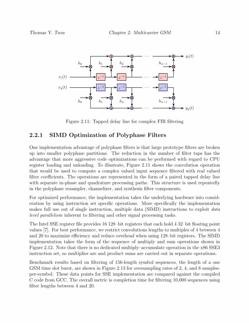
Figure 2.11: Tapped delay line for complex FIR filtering
2.2.1 SIMD Optimization of Polyphase Filters
One implementation advantage of polyphase filters is that large prototype filters are brokenup into smaller polyphase partitions. The reduction in the number of filter taps has theadvantage that more aggressive code optimizations can be performed with regard to CPUregister loading and unloading. To illustrate, Figure 2.11 shows the convolution operationthat would be used to compute a complex valued input sequence filtered with real valuedfilter coefficients. The operations are represented in the form of a paired tapped delay linewith separate in-phase and quadrature processing paths. This structure is used repeatedlyin the polyphase resampler, channelizer, and synthesis filter components.
For optimized performance, the implementation takes the underlying hardware into consid-eration by using instruction set specific operations. More specifically the implementationmakes full use out of single instruction, multiple data (SIMD) instructions to exploit datalevel parallelism inherent to filtering and other signal processing tasks.
The Intel SSE register file provides 16 128–bit registers that each hold 4 32–bit floating pointvalues [7]. For best performance, we restrict convolutions lengths to multiples of 4 between 4and 20 to maximize efficiency and reduce overhead when using 128–bit registers. The SIMDimplementation takes the form of the sequence of multiply and sum operations shown inFigure 2.12. Note that there is no dedicated multiply–accumulate operation in the x86 SSE3instruction set, so multiplies are and product sums are carried out in separate operations.
Benchmark results based on filtering of 156-length symbol sequences, the length of a oneGSM time slot burst, are shown in Figure 2.13 for oversampling rates of 2, 4, and 8 samples-per-symbol. These data points for SSE implementation are compared against the compiledC code from GCC. The overall metric is completion time for filtering 10,000 sequences usingfilter lengths between 4 and 20.

Thomas Y. Tsou Chapter 2. Multicarrier GSM 15
s3 s2 s1 s0q0
s7 s6 s5 s4q1
s11 s10 s9 s8q2
s15 s14 s13 s12q3
s19 s18 s17 s16q4
s3 s2
s1 s0
d1
d0
s1 s0d0
Red and blue shaded objectsrefer to in-phase and quadraturecomponents respectively
Load next set of shifted I and Qsamples into registers while leavingthe real filter taps in place
mm load ps()
Store result of inner productsum to memory
Quad-multiply
mm mul ps()
Compute product-sum
mm hadd ps()
mm store ss()
1
Figure 2.12: Intel SSE3 SIMD inner product summation for complex–real convolution with4 tap FIR filter. Usage of single, double, and quad registers is labeled.

Thomas Y. Tsou Chapter 2. Multicarrier GSM 16
10−2
10−1
100
4 8 12 16 20 24 32
Tim
e(s
econ
ds)
Filter Length
GCC - 2 spsGCC - 4 spsGCC - 8 spsSSE - 2 spsSSE - 4 spsSSE - 8 sps
Figure 2.13: Comparison of SSE assembly intrinsics (blue) vs. GCC generated (red) filteroperations. Displayed completion times are based on filtering of 10,000 GSM bursts of 2, 4,and 8 samples-per-symbol.

Thomas Y. Tsou Chapter 2. Multicarrier GSM 17
2.2.2 DFT Computation on Non-Contiguous Data
A key motivation for using the polyphase channelizer and synthesis filter implementation isthat we can replace as large number of multiplication operations with a single DFT. Thisgives us the advantage that very computationally efficient FFT methods can be used. Forthe implementation we utilize “Fastest Fourier Transform in the West” (FFTW), an opensource software package for computing discrete Fourier transforms. FFTW is well knownas the fastest freely available implementation of the FFT algorithm. Like the above SIMDoptimizations, FFTW also uses similar efficient SSE instructions internally for architecturespecific optimization.
Furthermore, FFTW elegantly handles the complex task of manipulating data storage whendealing with the filter bank inputs and outputs. The critical issue here is that each filterbank output writes data into individual continuous buffers. The DFT operates on a singlesample from each partition buffer such that the data accesses are across non-contiguousmemory storage. There are two approaches to handle this situation. First, the data canbe interleaved into continuous blocks for the FFT computation or, second, the FFT can becomputed on discontinuous data. For the latter each sample would be drawn with an offset,known as the stride count, related to the number of polyphase partitions.
Fortunately, FFTW is capable of operating on discontinuous data, so the second approachwas chosen to manipulate disjoint data directly and avoid unnecessary data interleaving orshuffling. Figure 2.14 demonstrates the data mapping and computation of a simplified M = 4configuration. For this configuration, a single call into FFTW performs 4 FFT operationsof size 4 on disjoint data. The buffer depth is also chosen to be 4. On the left side of thefigure there is a linear arrangement of continuous data buffers. The right side of the figureshows the element mapping for the FFT operation. This example implementation computes4 FFT operations of length 4 with a single function call.
2.3 Results and Discussion
We now provide overall operational results of the multicarrier BTS implementation. Figures2.15 and 2.16 demonstrate OpenBTS operation with 8 carriers on 8 MHz of combined uplinkand downlink bandwidth. The spectrum display shows uplink signals from 8 handsets onseparate carrier. Recall that each carrier has 8 physical channels, so this configuration hasmaximum capacity of 63 full rate voice channels after accounting for the broadcast beacon.For this example, handsets were allocated to separate carriers for demonstrative purposes.Deployed systems may use other channel assignment schemes.
Note that the signals shown on the spectrum display have a faint image because the handsetsare not continuously transmitting as they operate with Tx/Rx switching. Since each trafficchannel occupies a single physical TDMA channel, or 1/8th of the complete frame time, the

Thomas Y. Tsou Chapter 2. Multicarrier GSM 18
a0
a1
a2
a3
b0
b1
b2
b3
c0
c1
c2
c3
d0
d1
d2
d3
0x00
0x10
0x20
0x30
0x40
0x50
0x60
0x70
Mem
oryAddress
a0
b0
c0
d0
a1
b1
c1
d1
a2
b2
c2
d2
a3
b3
c3
d3
DFT computation on non-contiguous complex transform data usingmulti-dimensional fftwf plan many dft() operation and stride count
fftwexecute()
1
Figure 2.14: Vector optimization of 4x4 DFT on non-contiguous data

Thomas Y. Tsou Chapter 2. Multicarrier GSM 19
Figure 2.15: Multiple handset uplink channels allocated on separate carriers, span = 4 MHz
effective duty cycle of the mobile transmitter is below 15% after guard intervals are consid-ered. Also note that the spectrogram construction uses overlapped measurement windows,so the exact placement of bursts in time (Y-axis) relative to each other is not accurate. Amore precise representation would show subsequent bursts evenly spaced at the GSM frameperiod of 4.615 ms.
Figure 2.17 shows the downlink with a narrower span of 2 MHz. The beacon channel –with the noticeable FCCH peak right of the center frequency – is the leftmost signal. Forillustrative purposes, beacon signals are also activated on the non-primary channels - fornormal operation only the primary carrier would be broadcasting a continuous signal on alltime slots.
For performance comparisons, operational testing also consisted of single direction bench-marks in which only the downlink signal was enabled while using the highest available band-width possible. Figure 2.18 shows maximum supported bandwidth in the downlink only test.The synthesis filter is operating at the device limited bandwidth of 20 MHz in a 50 channelx 400 kHz configuration. The USRP2 support 25 MHz with 1 Gbps Ethernet, however, theOpenBTS transceiver requires a single receive to timestamp delivery and synchronization ofwith the USRP sample clock. Consequently, this receive channel limits higher sample ratesalthough CPU utilization may allow higher rates and more channels. Here, the transceiveris limited to a reduced maximum rate of 20 MHz.
Figure 2.19 shows the spectrogram output and that all channels are time synchronized.Internal to the software radio implementation, all transceivers are locked to the same GSMframe clock, which is an incremental time slot counter. Because all transmitters originatefrom a single baseband source, time synchronization is a trivial matter and significantly

Thomas Y. Tsou Chapter 2. Multicarrier GSM 20
Figure 2.16: Spectrogram showing timeslots of 8 carrier MCBTS traffic, 4 MHz span
Figure 2.17: MCBTS downlink (with activated secondary beacons), 2 MHz span

Thomas Y. Tsou Chapter 2. Multicarrier GSM 21
Figure 2.18: Synthesis filter output with 45 GSM channels, 20 MHz span
simpler than an implementation using physically separated transceivers.
2.4 Optional Features
For prior sections, the multicarrier operation was setup for 400 kHz channel separations,however, GSM specified spacing is actually 200 kHz with overlapping channels. For a max-imally packed GSM configuration, there is no requirement for supporting 200 kHz channelplacements because these channels would be self–interfering. There are other situations,however, where more flexible selection of frequencies is desired. In order to allow more flexi-bility in channel assignments, we now extend the existing design to allow any GSM channelselection.
In order to operate at 200 kHz instead of 400 kHz spacing, we need to double the numberof channels in the filter bank. To maintain the 400 kHz sampling rate, rather than halvingthe channelizer output, the individual channels are oversampled by a factor of two.
We primarily focus on the synthesis filter used to aggregate independent channels on thebase station downlink direction and, for brevity, we describe the implementation withoutderivation. Analysis of the oversampled filter bank can be found in [6].
Figure 2.20 shows the oversampled synthesis filter implementation for oversampling factorof two. Existing texts typically represent the oversampled filter bank with a cyclic , orserpentine, shift of the polyphase filters and the corresponding commutator phase. Theseshifts would then occur on alternating samples, or every other sample for a oversampling

Thomas Y. Tsou Chapter 2. Multicarrier GSM 22
Figure 2.19: Spectrogram with time synchronized signals, 10 MHz span
rate of two.
For the OpenBTS implementation we address the cyclic shift by deinterleaving even and oddsamples into separate filter banks with pre-shifted polyphase partitions. Note that in theactual implementation, the shifts are arranged with memory pointer swaps. The commutatorphase difference is absorbed into a second commutator on the second filter bank. The overalleffect is that the second filter bank is offset, or delayed, with respect to the first.
The end result is a great deal of flexibility including the capability to precisely place andoverlap GSM channels. At first glance, this feature may not seem particularly useful. Whenwe consider that the channelizing filter bank may be extended to interaction with other non-GSM signals, there is a high potential for use in more general applications. For example,Figure 2.21 shows an example of a composite signal constructed from 200 kHz channels anda GSM channel. With a 20 MHz filter bank, we assign roughly 10 MHz separation betweenthe two different signals.
As the figure shows, this configuration has the capability of running two distinct waveforms,which both originate from a single time synchronized baseband in conjunction with an ex-isting 10 MHz LTE signal. In this case, the LTE signal is a commercial over-the-air signal at751 MHz. In an isolated test environment, the filter bank output transmits above and belowthe LTE signal without interfering. As the spectrum capture shows, given enough basebandbandwidth, the filter bank gives us the ability to operate with a great deal of flexibility onnon-contiguous spectrum assignments.

Thomas Y. Tsou Chapter 2. Multicarrier GSM 23
h0(n)
h1(n)
h2(n)
h3(n)
h2(n)
h3(n)
h0(n)
h1(n)
DFT
v0(m)
v1(m)
v2(m)
v3(m)
v0(m)
v1(m)
v2(m)
v3(m)
Eve
nsa
mpl
es
Odd
samples
Y0(m)
Y1(m)
Y3(m)
Y2(m)
+v(n)
Each filter bank runs at halfthe input sample rate.
1
Figure 2.20: 2x oversampled synthesis filter implementation
Figure 2.21: Non-contiguous spectrum usage with 10 MHz LTE signal between composite(left) and GSM (right) signals, 16 MHz span

Chapter 3
Improved Signal Integrity withLinearized GMSK
The GSM standard specifies Gaussian minimum-shift keying (GMSK) as the modulationscheme, which determines the metrics that are used for characterizing signal integrity andperformance [8]. In a operational system, such as OpenBTS, there are many factors thataffect transmit signal performance prior to reaching the power amplifier: DC offset, IQimbalance, sampling, and phase noise among others. But, certain factors are hardwarerelated and others are inherent to the design and implementation of the digital transmitteritself; the focus of this chapter is on the latter.
More specifically, this chapter traces signal integrity in the form of 3GPP specified phaseerror from the hardware output to the core design of the GMSK transmitter. For this process,definitive measurements are made with a GSM specific signal analyzer. We will show thatthe GSM requirements for GMSK signal quality are not particularly strict and that there issignificant margin for improvement beyond minimum compliance values.
3.1 GSM Modulation
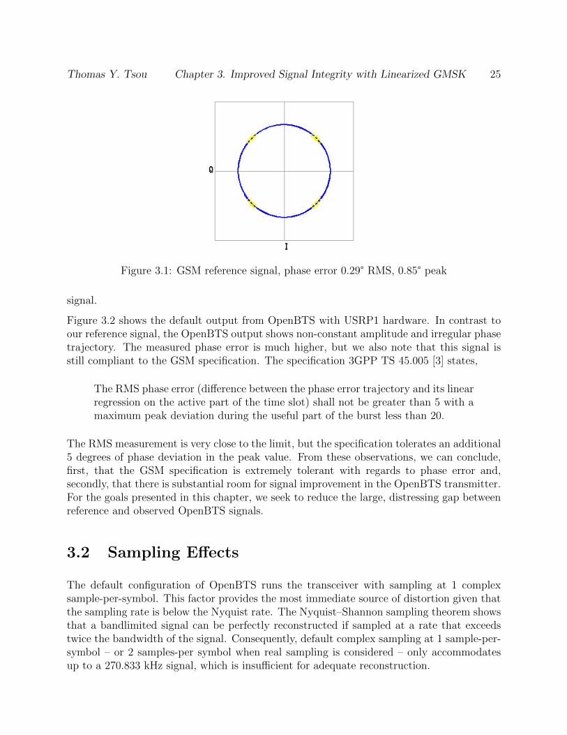
A GSM test signal generated by a commercial cellular signal generator (Agilent E4438C) isshown in Figure 3.1. The receiving and measuring device is a corresponding cellular signalanalyzer (E4406A) of the same manufacturer. We note two defining characteristics of theGSM modulation. First, there is the very clear constant envelope and circular phase path.Second, the sampling points (in yellow) form small cluster of three distinct locations; theclustering is the result of intersymbol interference, ISI, of the partial response Gaussian pulse,which will be explained in following sections. Unsurprisingly for calibrated and certifiedcommercial test equipment, measured phase error – the RMS and peak phase deviationcompared to an ideal signal – is very low at below 1° and demonstrates an extremely accurate
24
Thomas Y. Tsou Chapter 3. Improved Signal Integrity with Linearized GMSK 25
Figure 3.1: GSM reference signal, phase error 0.29° RMS, 0.85° peak
signal.
Figure 3.2 shows the default output from OpenBTS with USRP1 hardware. In contrast toour reference signal, the OpenBTS output shows non-constant amplitude and irregular phasetrajectory. The measured phase error is much higher, but we also note that this signal isstill compliant to the GSM specification. The specification 3GPP TS 45.005 [3] states,
The RMS phase error (difference between the phase error trajectory and its linearregression on the active part of the time slot) shall not be greater than 5 with amaximum peak deviation during the useful part of the burst less than 20.
The RMS measurement is very close to the limit, but the specification tolerates an additional5 degrees of phase deviation in the peak value. From these observations, we can conclude,first, that the GSM specification is extremely tolerant with regards to phase error and,secondly, that there is substantial room for signal improvement in the OpenBTS transmitter.For the goals presented in this chapter, we seek to reduce the large, distressing gap betweenreference and observed OpenBTS signals.
3.2 Sampling Effects
The default configuration of OpenBTS runs the transceiver with sampling at 1 complexsample-per-symbol. This factor provides the most immediate source of distortion given thatthe sampling rate is below the Nyquist rate. The Nyquist–Shannon sampling theorem showsthat a bandlimited signal can be perfectly reconstructed if sampled at a rate that exceedstwice the bandwidth of the signal. Consequently, default complex sampling at 1 sample-per-symbol – or 2 samples-per symbol when real sampling is considered – only accommodatesup to a 270.833 kHz signal, which is insufficient for adequate reconstruction.

Thomas Y. Tsou Chapter 3. Improved Signal Integrity with Linearized GMSK 26
Figure 3.2: OpenBTS default configuration, phase error 4.98° RMS, 14.95° peak
Figures 3.3 and 3.4 show the spectrum of oversampled and undersampled OpenBTS signalsrespectively. Each capture shows 1 MHz of spectrum with 10 dB increments on the Y-axis.Note that in the oversampled spectrum the occupied bandwidth (roughly 300 kHz at 99%of total signal power) exceeds the available complex sampling bandwidth of the 1 sample-per-symbol case. This undersampling is further compounded by downstream filtering bythe USRP hardware, which creates additional aliasing. Consequently, given the observablespectrum distortion, we can conclude that the signal shown in Figure 3.2 suffers from thedetrimental effects of undersampling.
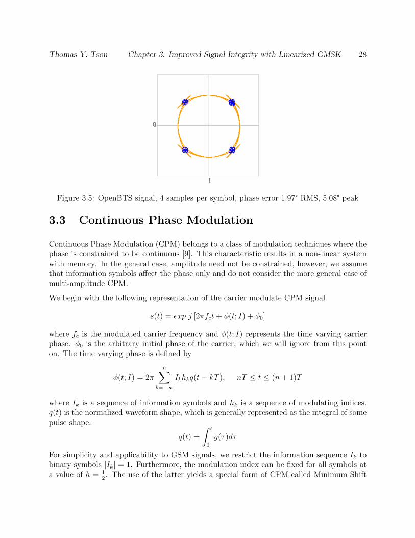
Therefore, increasing the sample rate is the first step to improving transmit signal quality;the same OpenBTS signal sampled at 4 samples-per-symbol is shown in Figure 3.5. Though2 samples per symbol would be sufficient from a standalone DSP perspective, these examplesare further oversampled to 4 samples-per-symbol for the purpose of reducing filter distortiongenerated on the USRP devices. The CIC (cascaded integrator-comb) filters located on thedevice apply a sinc shaped frequency response to the input signal, which we can reduce byoversampling.
Given sufficient sampling rate, we now observe a much cleaner phase trajectory and moreaccurate sampling points. Phase error is now well below the requirement for GSM compli-ance. Note, though, that there are remaining phase artifacts that were clearly not present inthe reference signal of Figure 3.1 Resolving these phase path effects, which are not a result ofsampling, requires a much deeper examination into the design of the OpenBTS modulator.The phase artifacts are a result of the fact the transmitter does not use an exact, direct formGMSK modulator, but instead uses a linearized approximation of GMSK. In order to furtherpursue the source of these effects, we need to understand the theory and representations ofGMSK and the broader class of continuous phase modulations.

Thomas Y. Tsou Chapter 3. Improved Signal Integrity with Linearized GMSK 27
Figure 3.3: Oversampled OpenBTS spectrum with 8 samples-per-symbol, 1 MHz span
Figure 3.4: Undersampled OpenBTS spectrum with 1 samples-per-symbol, 1 MHz span
Thomas Y. Tsou Chapter 3. Improved Signal Integrity with Linearized GMSK 28
Figure 3.5: OpenBTS signal, 4 samples per symbol, phase error 1.97° RMS, 5.08° peak
3.3 Continuous Phase Modulation
Continuous Phase Modulation (CPM) belongs to a class of modulation techniques where thephase is constrained to be continuous [9]. This characteristic results in a non-linear systemwith memory. In the general case, amplitude need not be constrained, however, we assumethat information symbols affect the phase only and do not consider the more general case ofmulti-amplitude CPM.
We begin with the following representation of the carrier modulate CPM signal
s(t) = exp j [2πfct+ φ(t; I) + φ0]
where fc is the modulated carrier frequency and φ(t; I) represents the time varying carrierphase. φ0 is the arbitrary initial phase of the carrier, which we will ignore from this pointon. The time varying phase is defined by
φ(t; I) = 2πn∑
k=−∞Ikhkq(t− kT ), nT ≤ t ≤ (n+ 1)T
where Ik is a sequence of information symbols and hk is a sequence of modulating indices.q(t) is the normalized waveform shape, which is generally represented as the integral of somepulse shape.
q(t) =
∫ t
0
g(τ)dτ
For simplicity and applicability to GSM signals, we restrict the information sequence Ik tobinary symbols |Ik| = 1. Furthermore, the modulation index can be fixed for all symbols ata value of h = 1
2. The use of the latter yields a special form of CPM called Minimum Shift

Thomas Y. Tsou Chapter 3. Improved Signal Integrity with Linearized GMSK 29
Keying (MSK). We can rewrite the phase of MSK as
φ(t; I) =1
2π
n−1∑
k=−∞Ik + πInq(t− kT ), nT ≤ t ≤ (n+ 1)T
= θn +1
2πIn
(t− nTT
)
Here θn is the accumulation of previous phase shifts up to symbol n. Consequently, we havea representation where the current phase at time t is represented by summed previous phaseshifts and a positive or negative π
2shift for the current symbol. From this point forward, we
primarily consider the MSK case where h = 12.
3.4 Laurent Decomposition of CPM Signals
As an alternate representation, CPM can be constructed as a linear combination of a finitesequence of pulses. This second approach provides an additional method that can be used inthe modulation or demodulation process. We will discuss in later implementation sections asto why such an approach is desirable. But, for now, the linearized approach has the benefit ofsimpler and more convenient implementation and implications towards modulations used inmore recent standards. Originally described by Pierre Laurent in 1986 [10], we now providethe linear representation of CPM and follow with a representation for 0.30 BT GMSK thatis used for GSM.
We begin with the previous low-pass representation and ignoring the initial phase offset.
s(t) = exp j [φ(t; I)]
with the time varying phase described by
φ(t; I) = 2πn∑
k=−∞Ikhkq(t− kT ), nT ≤ t ≤ (n+ 1)T
which we can use to rewrite the signal as
eφ(t;I) = exp
(jπh
n−L∑
k=−∞
)L−1∏
k=0
exp [j2πhIn−kq (t− (n− k)T )]
Laurent then introduces the generalized phase pulse function that is derived from the phaseshift of the signal. This important function has non-zero values from 0 ≤ t ≤ 2LT and isspecified by
s0(t) =sin (ψ(t))
sinπh

Thomas Y. Tsou Chapter 3. Improved Signal Integrity with Linearized GMSK 30
where
ψ(t) = 2πhq(t) t < LT
ψ(t) = πh− 2πhq(t− LT ) LT ≤ t
This function serves as the basis for constructing the pulse series that will constitute thecomplete linear representation of the signal. The pulses ck(t) for 0 ≤ k ≤ 2L−1 are definedby
ck(t) = s0(t)L−1∏
n=1
s0 (t+ (n+ Lak,n)T ) , 0 ≤ t ≤ Tminn [L(2− ak,n)− n]
Each pulse is weighted by a complex coefficient where
Ak,n =n∑
m=−∞Im −
L−1∑
m=1
In−mak,m
k =L−1∑
m=1
2m−1ak,m, k = 0, 1, 2, · · · , 2L−1 − 1
ak,m = 0 or 1
Given the above phase pulses, substituting and reorganization of terms in the signal functionyields the final result
eφ(t;I) =∑
n
2L−1−1∑
k=0
ejπhAk,nck(t− nT )
which is the CPM signal represented by finite sum of weighted pulses.
3.4.1 GMSK Laurent Decomposition for L=3
As an supplementary example to the mathematical representation, the effects of Laurentdecomposition can be shown through graphical comparison. We examine the case for L = 3,which can be easily shown to be sufficient for GMSK with a 0.30 bandwidth time product.The first three generated pulses (named C0, C1, and C2) for BT = 0.30 are shown inFigure 3.6
From the preceding analysis, we can construct our CPM signal with a finite number of pulses,but Figure 3.6 shows that the practical number of pulses may be an even smaller numberthan the mathematical representation specifies. In this case the plot shows that only thefirst two pulses are of any significant magnitude, while the third pulse, C2, is barely visible.Furthermore, the primary pulse, C0, is overwhelmingly dominant. In fact, the C0 pulsealone is sufficient for a linearized approximation of the GMSK modulation, which is used by

Thomas Y. Tsou Chapter 3. Improved Signal Integrity with Linearized GMSK 31
0
0.2
0.4
0.6
0.8
1
-2 -1 0 1 2
Am
plitu
de
Sample Number
c0c1c2
Figure 3.6: Laurent C0, C1, and C2 pulses for BT = 0.30
OpenBTS and measured in Figure 3.5. But, as we observed, there are remaining artifactsdue to the missing C1 pulse, which, though small, are not insignificant.
For comparison purposes, we can also examine the generated Laurent pulses for varyingwidths of the original partial response Gaussian shape. Figures 3.7 and 3.8 show the com-puted pulses for BT = 0.20 and BT = 0.40 respectively. In all cases we find negligiblesignificance of pulses beyond C0 and C1. We also find an increase in significance of theC1 pulse as the BT product, and ISI, decreases. This is expected since as the BT productapproaches infinity, the partial response GMSK signal becomes a normal full response MSKsignal, which can be fully represented by linear representation equivalent to offset-QPSKwith a half-sinusoidal pulse shape.
3.5 Implementation
Given the linearized representation of CPM, we can now proceed to the actual softwareimplementation. In this section, we directly translate the analytical work of Laurent into afully operational real time GMSK modulator. The initial OpenBTS design, which uses singleC0 pulse implementation is shown in Figure 3.9. The implementation consists of an inputbit sequence mapped to either a positive or negative phase shift of πh = π
2. The phase shift
is then accumulated and sent to the pulse shaping filter. Note that GSM employs differentialencoding, which is not shown.
In order to add the second C1 pulse, Laurent’s decomposition translates to the structure ofFigure 3.10. While there is an expanded structure to accommodate the effect of one delayedsignal, the operations for MSK, h = 1
2, are simply bit inversions in the in-phase or quadrature

Thomas Y. Tsou Chapter 3. Improved Signal Integrity with Linearized GMSK 32
0
0.2
0.4
0.6
0.8
1
-2 -1 0 1 2
Am
pli
tud
e
Sample Number
c0c1c2
Figure 3.7: Laurent C0, C1, and C2 pulsesfor BT = 0.20
0
0.2
0.4
0.6
0.8
1
-2 -1 0 1 2
Am
pli
tud
e
Sample Number
c0c1c2
Figure 3.8: Laurent C0, C1, and C2 pulsesfor BT = 0.40
an∑
ejπhA0,N
ejπh
s(t) =∑∞N=−∞ J
A0,N [A0,NC0(t−NT ) + J−aN−1C1(t−NT )]
A0,N =∑Ni=−∞ ai
A1,N = A0,N − aN−1
A2,N = A0,N − aN−2
A3,N = A0,N − aN−1 − aN−2
1
Figure 3.9: Linearized GMSK symbol mapper with single pulse
channels. Filtering and summing with the C0 and C1 pulse shapes can be implemented witha structure that resembles two conjoined tapped delay lines as shown in Figure 3.11. Thetap lengths in this case represent computed pulse filters at 4 samples-per-symbol.
3.6 Results and Discussion
With the advantages of the linearized approach, our pulse simulations showed that we caneasily ignore all pulses except for C0 and C1. That led us to the construction given inFigures 3.11 and 3.10. We also know that we can only use the C0 pulse for a very simpleimplementation, but then suffer from the phase trajectory artifacts shown at the beginning ofthis chapter. The USRP1 output of our final construction is shown in Figure 3.14 alongsidethe original single pulse implementation at 1 and 4 samples per symbol in Figure 3.12 andFigure 3.13 respectively.
Given the modified GMSK modulator of Figure 3.14, we can clearly observe the absence ofphase artifacts present in the original modulator, Figure 3.13. Obviously, both cases showsubstantial improvements from the sub-Nyquist samples case of Figure 3.2. While modifyingthe OpenBTS modulator shows clearly visible improvements in the magnitude error near thesampling points, the improvement in measured phase error is quite modest. To find out why,

Thomas Y. Tsou Chapter 3. Improved Signal Integrity with Linearized GMSK 33
In∑
ejπhA0,n
ejπh
z−1 ejπhA0,ne−jπhIn−1
e−jπhIn−1
e−jπhIn
s(t) =∑∞n=−∞ e
jπhA0,n [c0(t− nT ) + e−jπhIn−1c1(t− nT )]
A0,n =∑nm=−∞ Im
A1,n = A0,n − In−1
In = 1,−1
1
Figure 3.10: Linearized GMSK symbol mapper with C0 and C1 pulses
ejπhA0,n z−1 z−1 z−1 z−1 z−1 z−1
s(t)
ejπhA0,ne−jπhIn−1 z−1 z−1
1
Figure 3.11: Combined tapped delay line for linearized GMSK pulses C0 and C1

Thomas Y. Tsou Chapter 3. Improved Signal Integrity with Linearized GMSK 34
Table 3.1: Measured Phase Error
Samples-per-symbol RMS Peak3GPP TS 45.005 N/A 5.00 20.00
USRP1, C0 1 4.89 14.25USRP1, C0 4 1.92 5.44
USRP1, C0 and C1 4 1.66 4.53USRP2, C0 and C1 4 1.14 2.97
we can measure the same modulator implementation through an USRP2, which is displayedin Figure 3.15.
The USRP2 shows superior phase accuracy – recall that the GSM compliance phase erroris 5° RMS and 20° peak. The summary of various modulator and hardware combinationsdiscussed in this chapter are shown in Table 3.1. In the USRP2 case, the primary differencebetween USRP1 and USRP2 measurements are due to the availability of DC offset and IQimbalance corrections on the USRP2. Both combinations use the same WBX daughterboardfrom Ettus Research, but only the USRP2 supports automatic daughterboard calibration.Consequently, we can conclude that, to a large extent, we are no longer primarily observingGMSK modulator irregularities, but the effects of uncompensated RF hardware differences.
The linear modulation approach described in this chapter, at first glance, seems unneces-sary and cumbersome given that a basic GMSK implementation with a pulse shaped bitsequence driving a phase accumulator is not particularly complex. There are, however, threesignificant advantages of the linearized approach. First, the modulator can be implementedusing only standard multiply-accumulate operations. This contrasts to the direct imple-mentation of MSK that drives a frequency modulator using trigonometric methods, whichmay be difficult to implement or optimize depending on the processor architecture. Sec-ond, while GMSK modulation is constant amplitude, the TDMA based GSM signal is not.Time slots in GSM are separated by guard intervals with specified amplitude ramp-up andramp-down requirements [2]. Consequently, the implementation does need to consider am-plitude changes, and the linear approach can provides a simpler implementation. Finally,there are strong implications for the linearized approach because of developments in laterspecifications. For example, the linearized Gaussian pulse shape is explicitly specified foruse in 8-PSK EDGE [8]. Furthermore, the same pulse shape is used again with a modifiedQPSK modulation in the more recent Release 9 specification for orthogonal subchannels andvoice, VAMOS [4]. Given these concerns, the linearized approach to GMSK turns out to bevery reasonable for GSM targeted implementations.

Thomas Y. Tsou Chapter 3. Improved Signal Integrity with Linearized GMSK 35
Figure 3.12: OpenBTS–USRP1 phase error,1 sample per symbol, C0 pulse, 4.98° RMS,14.95° peak
Figure 3.13: OpenBTS–USRP1 phase error,4 samples per symbol, C0 pulse, 1.92° RMS,5.44° peak
Figure 3.14: OpenBTS–USRP1 phase error,4 samples per symbol, C0 and C1 pulses,1.66° RMS, 4.53° peak
Figure 3.15: OpenBTS–USRP2 phase error,4 samples per symbol, C0 and C1 pulses,1.14° RMS, 2.97° peak

Chapter 4
Embedded BTS
Chapter 2 explored the task of maximizing OpenBTS user capacity with a wideband multi-carrier implementation. In Chapter 3, we increased OpenBTS signal integrity substantiallybeyond requirements set forth by 3GPP specifications. In this chapter, rather than pushingany upper limits, we attempt to reduce certain properties by running OpenBTS on small,embedded form factor.
The overall system assumption of previous chapters consisted of a comparatively powerfulx86 host machine interfacing with a USRP radio device. Now, we consider the case of muchsmaller, and less power hungry, processor combinations. Specifically, an ARM applicationprocessor and DSP processor from Texas Instruments will be compared. We will introduceand discuss the E100 hardware platform from Ettus Research that encompasses these proces-sors and follow with comparative results based on filtering metrics similar to those presentedin Chapter 2. Our final result will evaluate single carrier OpenBTS operation on the embed-ded platform with a NEON optimized and fixed point DSP transceiver implementation.
4.1 Hardware Platform Description
The E100 platform is a USRP variant that includes three reconfigurable processors suitablefor different aspects of software radio and cellular use: Xilinx Spartan-3A FPGA, ARMCortexA8, and Texas Instruments fixed point C64x+ DSP. The general purpose ARM pro-cessor (GPP) and C64x+, as components of the TI OMAP3530 application processor, arecollocated on a removable Gumstix computer-on-module board [11]. The FPGA is mounteddirectly on the main board and interfaces with the other processors through a combina-tion of General Purpose Input / Output (GPIO) pins and the OMAP3530 General PurposeMemory Controller (GPMC). The overall processor structure and connections are shown inFigure 4.1. Since we are primarily interested in signal processing and optimized computation,the remainder of this chapter focuses on the ARM and DSP elements.
36

Thomas Y. Tsou Chapter 4. Embedded BTS 37
Figure 4.1: E100 multi-processor platform
4.1.1 Interprocessor Communication
Distribution of base station functionality across the set of multiple, heterogeneous processorsgreatly improves efficiency and increases the capabilities of the device, but introduces theadded task of managing interprocessor communication across each of the different cores.Because of disparate physical locations, interconnects, and the unique characteristics of eachprocessor, no unified software architecture for interprocessor communication exists for theE100 configuration. Rather, interaction between the specialized DSP and FPGA cores andthe GPP occurs through separate, independently implemented software interfaces. Also,no direct FPGA–DSP line of interaction is implemented. Consequently, all communicationflows through the ARM processor. While less optimal than a directly mapped FPGA–DSPinterface, this approach results in a far less complex implementation and significantly reduceddevelopment time.
ARM to C64x+ transfers are implemented using TI DSP/BIOS Link (DSPLINK), whichprovides an interface and abstraction layer for a shared memory and hardware interruptbased transport. The overall GPP–DSP message queue transport is shown in Figure 4.2.During initialization, asynchronous message buffers are allocated from a shared memory pool.Through DSPLINK, OpenBTS uses message queues for transferring shared memory pointersto and from the DSP; these memory pointers reference buffers containing the bursts receivedfrom the FPGA. Either side of the connection can access the shared buffer contents bytranslating the pointer address between the ARM and DSP virtual address spaces. The datain memory is then read or written by explicit cache invalidations or cache writes respectively.
As a TDMA based standard, reception and transmission of GSM signals is heavily dependenton segmentation of continuous data streams into independent, synchronized time slots, or

Thomas Y. Tsou Chapter 4. Embedded BTS 38
Figure 4.2: C64x shared memory transport
bursts. Consequently, due to time slot use, the message and queuing mechanism facilitates anefficient and fitting abstraction for communicating sampled GSM data across the GPP–DSPbarrier.
4.2 GSM Transceiver
The embedded BTS implementation partitions base station functionality across multipleprocessors in order to support different aspects of GSM operation in an efficient manner. Theprecise timing necessary to meet the strict, real-time requirement of GSM specific TDMAaccess is managed through coordinated use of the ARM and FPGA cores. The FPGAconfiguration is mandatory since no other processor on the device has the necessary hardtiming capability. The task of partitioning functionality between the ARM and C64x DSPcores is somewhat less clear. As an embedded application processor, the ARM is heavilyconstrained compared to the larger x86 based systems. Therefore, maximizing use of theDSP is the preferred approach, but, frequent data transactions between the two cores incurtransport and signalling penalties that must be considered.
One approach to transceiver partitioning is to split transmit and receive chains across dif-ferent processors. With this approach, there are no dependencies as each signal path isseparately handled. In addition, the previous chapter demonstrated that the GSM modula-tor can be constructed with a simplified linearized GMSK implementation; we showed thatthe transmitter design consists of a symbol mapper and modified pulse shaping filter. Incontrast, the OpenBTS receiver structure, which we have not yet examined, must handlemore complicated tasks of burst detection, timing recovery, and demodulation. As a re-

Thomas Y. Tsou Chapter 4. Embedded BTS 39
Figure 4.3: OpenBTS L1/PHY transmit chain
sult of these differences, allocating the receiver chain to the DSP and performing transmitmodulation on the ARM creates an appropriate partitioning.
4.2.1 Transmitter Structure
The linearized GMSK (LGMSK) modulator from Chapter 3 can be implementation throughfiltering and therefore the successive use of multiply–accumulate operations. Consequently,we can modify the implementation with SIMD approaches not unlike those performed forthe polyphase multicarrier implementation from Chapter 2. These changes will be describedin the later SIMD section.
Figure 4.3 shows the more general transmit chain beyond GMSK modulator. Within thetransmit chain, the overall burden of the modulation process is quite small. Note that inOpenBTS, forward error correction is implemented separately from the transceiver program,so we do not consider convolutional coding or decoding processes in this thesis.
4.2.2 Receiver Structure
The OpenBTS receiver chain is shown in Figure 4.4 and encompasses all portions of theGSM physical layer. Our focus in this section is primarily on porting the GSM receiverto the C64x DSP. Since we maintain the high-level receiver design, thorough discussion ofthe design itself is beyond the scope of this thesis. The essential elements, however, willbe briefly introduced. As with the transmitter, we note that forward error correction isconsidered separately from the receiver.
Given the discontinuous nature of GSM TDMA communications – there is no continuity insample timing or phase between bursts – timing and synchronization are heavily based on

Thomas Y. Tsou Chapter 4. Embedded BTS 40
Figure 4.4: OpenBTS L1/PHY receive chain
the use of embedded training sequences [12]. These training sequences exist as midamblescentered within the GSM burst structure. As Figure 4.4 shows, the output of the midambledetection, a correlation operation, is used for timing recovery, which consists of fractionaldelay filtering, and phase correction. While we do not discuss these operations in furtherdetail, the critical characteristic of all these processes is that they can be implemented usingsome form of polyphase filter bank or convolution method.
For example, midamble detection is implemented through cross correlation, which is anal-ogous to convolution. Also, fractional delay filtering is an interpolation process that isefficiently implemented with a polyphase filter bank. Consequently, the task of implemen-tation and optimization of the receiver is highly reflective of the previous approaches andanalysis provided in Chapter 2.
4.3 Implementation
4.3.1 ARM SIMD
In comparing ARM to the x86 SIMD architecture presented in Chapter 2, there are veryclose similarities such as the use of quad–word operations and a register bank of 16 128-bitregisters [13]. Again, OpenBTS uses single precision 32-bit floating point values. There are,however, significant variations that can be traced to fundamental differences in the x86 andARM architectures. The ARM processor is a load/store architecture in that data stored in

Thomas Y. Tsou Chapter 4. Embedded BTS 41
a0
b0
a1
b1
a2
b2
a3
b3
a4
b4
a5
b5
a6
b6
a7
b7
0x00
0x04
0x08
0x0c
0x00
0x10
0x14
0x18
0x1c
0x20
0x24
0x28
0x2c
0x30
0x34
0x38
Mem
oryAddress
a3 a2 a1 a0a7 a6 a5 a4
b3 b2 b1 b0b7 b6 b5 b4
Q0Q1
Q2Q3
Figure 4.5: NEON quad–register 8 element multi–lane load for deinterleaving I and Q data
memory is never accessed directly, but always imported and exported to and from registerswith explicit load and store instructions. This approach contrasts with the x86 architecturethat allows instructions to directly or indirectly access memory values without an explicitload/store instruction. Given this characteristic, the ARM instruction set provides someadditional flexibility with loading stored sampled data.
Deinterleaving Register Load
One advantage of the ARM instruction set is that register loads can simultaneously deinter-leave from memory. This feature is beneficial for software-defined radio because samples arecommonly stored in interleaved I and Q format. For example, the USRP, GNU Radio, andOpenBTS all follow this convention of storing sampled data in alternating I and Q samples.Figure 4.5 demonstrates this deinterleaving capability with an 8-element complex load se-quence. In contrast, to perform the equivalent operation, the x86 architecture requires eitherindependent, separate loads, or a linear load followed by in-register shuffling of data.

Thomas Y. Tsou Chapter 4. Embedded BTS 42
NEON Multiply–Accumulate
Unique to the NEON instruction set is the availability of dedicated multiply–accumulateinstructions. The VMLA instruction performs a 4-element floating point multiply–accumulate,which, upon first glance, appears to be highly advantageous for use in SDR signal processing.With further examination, however, this instruction is not without significant performancelimitations. Figure 4.6 illustrates a successive complex multiply–accumulate as would beperformed for a FIR filter or other convolution based operation.
The limitation with the ARM VMLA instruction is due to idle delays in instruction pipeliningof the ARM Cortex–A8 architecture. More specifically, Cortex–A8 uses a 13 stage pipelinewith no out-of-order execution of instructions [14]. The critical limitation arises when twoVMLA instructions are used back-to-back – as would be performed for SDR filtering purposes.This condition causes a read-after-write (RAW) hazard, which leads to a pipeline stall ofmultiple cycles. The duration of the stall depends on the subsequent instructions. ForVMLA the effect is a rather significant 8 instruction cycles. Given that out-of-order executionis not supported, this behavior effectively reduces the advantages of hardware instructionpipelining when the VMLA instruction is used.
For comparison, the instruction path shown in Figure 4.7, which is very similar to theprevious x86 SSE case, does not have any dependencies through the first sequence of multiplyoperations. Consequently, this sequence, which does not utilize the hardware multiply–accumulate instruction, computes the same function with more instructions, yet completesfaster by a notable margin.
4.3.2 Texas Instruments C64x+ DSP
In comparison to previously discussed ARM and x86 processors, the C64x DSP is uniquein that it is not used as a standalone processor. Rather than running a general purposemultitasking operating system like Linux, the DSP runs a true real time operating system(RTOS) from Texas Instrument called DSP/BIOS. Then there is the difference in that theC64x is a fixed point processor where any floating point operations are performed strictlythrough software emulation.
As one would expect, the architecture differences of the specialized DSP processor are alsosubstantial. Figure 4.8 shows the basic architecture of a C6000 series DSP of which theC64x is a member. Like the ARM processor, the DSP is a load/store architecture in thatall memory accesses are performed by explicit load or store instructions. Unlike the ARM –or more specifically the Cortex–A8 – the C64x is a pipelined architecture with the followingfunctional units that can execute in parallel with no interdependencies.
• .D (.D1 and .D2) data load and store

Thomas Y. Tsou Chapter 4. Embedded BTS 43
s0 s1 s2 s3 s4 s5 s6 s7
s0 s1 s2 s3 s4 s5 s6 s7
Second Multiply-Accumulate (dashed)contains causes read-after-write(RAW) dependency and leads topipeline stall
Vector Multiply Accumulate
vmla.f32
Stored in-phase (red) and quadrature (blue) sampledata and real filter tap values
s0 s1 s2 s3 s4 s5 s6 s7
s8 s9 s10 s11
s12 s13 s14 s15
s16 s17 s18 s19
s20 s21 s22 s23
Figure 4.6: NEON multiply-accumulate instruction VMLA causes read after write (RAW)hazard

Thomas Y. Tsou Chapter 4. Embedded BTS 44
s0 s1 s2 s3 s4 s5 s6 s7
s0 s1 s2 s3 s4 s5 s6 s7
Quad-multiply
vmul.f32
Quad-sum
vadd.f32
Stored in-phase (red) and quadrature (blue) sampledata and real filter tap values
s0 s1 s2 s3 s4 s5 s6 s7
s8 s9 s10 s11
s12 s13 s14 s15
s16 s17 s18 s19
s20 s21 s22 s23
s24 s25 s26 s27
s28 s29 s30 s31
Figure 4.7: NEON 8 tap convolution product-sum with pipeline compatible operations (onlyfirst sum is shown)

Thomas Y. Tsou Chapter 4. Embedded BTS 45
L1 Program Memory
Instruction Fetch
L1 Data Memory
.L1
.M1
.S1
.D1
.L2
.M2
.S2
.D2
Register File A Register File B
Figure 4.8: Texas Instruments C64x DSP
• .S (.S1 and .S2) shift, branch, or compare
• .M (.M1 and .M2) multiply
• .L (.L1 and .L2) logic and arithmetic
Practically speaking, we see significant differences in the handling of iterative multiply–accumulate operations. Whereas the VMLA operation would essentially seize the Cortex–A8pipeline, the DSP is capable of processing two multiply-and-accumulate operations in a singlecycle. Now, to be fair, we use 32-bit floating point values on the ARM and 16 and 32 bitfixed point values on the DSP, so architectural comparison is an inexact process. Illustratingthese differences does, however, provide insight into the appropriate methods to approachingsignal processing tasks.
For implementation and code, the DSP is also unique in the tools and optimization process.Unlike the ARM where we relied on manual optimization with NEON instructions, DSPdevelopment is heavily dependent on the tool chain, compiler, and static analysis with lessemphasis low level operations. This concept is easily illustrated with the following codeexample and compiler output.

Thomas Y. Tsou Chapter 4. Embedded BTS 46
#pragma MUST_ITERATE(4, 16, 4)
for (i = 0; i < count; i++) {
prod = a[i] * b[i];
sum += prod;
}
*------------------------------------------------------------------*
* SOFTWARE PIPELINE INFORMATION
*
* Loop Unroll Multiple : 2x
* Known Minimum Trip Count : 2
* Known Maximum Trip Count : 8
* Known Max Trip Count Factor : 2
* Loop Carried Dependency Bound(^) : 0
* Unpartitioned Resource Bound : 1
* Partitioned Resource Bound(*) : 2
* Resource Partition:
* A-side B-side
* .L units 0 0
* .S units 0 1
* .D units 1 1
* .M units 1 0
*
* Total cycles (est.) : 9 + trip_cnt * 2 = Between 13 and 25
*------------------------------------------------------------------*
The code example consists of an iterative multiply and accumulate. A pragma directive is alsoinserted to signify that iteration values range from 4 to 16 with multiples of 4. The optimizingC6000 compiler output provides us with notable characteristics about the generated codesuch as unrolling and an estimate of the total cycle count. These cycle counts will laterprovide a point of comparison for evaluating DSP transport and overhead.
4.4 Results and Discussion
NEON Benchmarks
Benchmarking the different embedded approaches took the same form as the SIMD tests usedin Chapter 2. All measurements show averaged completion times for 10,000 convolutions onrandom GSM burst data. Bursts are 156 symbols and sampled at 2, 4, and 8 samples-per-symbol with varying

Thomas Y. Tsou Chapter 4. Embedded BTS 47
10−1
100
101
102
4 8 12 16 20 24 32
Tim
e(s
econ
ds)
Filter Length
GCC - 2 spsGCC - 4 spsGCC - 8 sps
NEON VMUL - 2 spsNEON VMUL - 4 spsNEON VMUL - 8 spsNEON VMLA - 2 spsNEON VMLA - 4 spsNEON VMLA - 8 sps
Figure 4.9: NEON vmul/vsum vs. vmla comparison
Figure 4.9 shows the comparison between using the GCC compiled C code output, multiply–accumulate instruction (VMLA), and pipeline optimized NEON approach. The comparisonshows large differences – an order of magnitude – between both versions of NEON code andthe compiled C code. The SIMD speedups are significantly larger than those seen on x86and also much higher than a factor of 4 that may be expected from quad-vector operations.This disparity is mostly attributed to GCC, which is very limited when generating NEONcode as discovered by examination of the generated assembly.
Within the two NEON implementations, the differences are more modest, but clearly benefi-cial. We conclude that for the our application with OpenBTS, the existence of the dedicatedmultiply–accumulate operation in the ARM instruction set provides little to no benefit.Furthermore, the use of NEON optimization is essential due to poor compiled C code per-formance.
DSP Benchmarks
Comparing DSP output is more complicated than NEON assembly because of the addedoverhead of interprocessor communication. Figure 4.10 shows completion times comparedto static analysis, or theoretical values. A constant DSP message size of 32 kB, equal tothe maximum size of the L1 data cache, was used for all tests and implementations. Thereare two notable characteristics in this comparison related to interprocessor communication

Thomas Y. Tsou Chapter 4. Embedded BTS 48
0
0.5
1
1.5
2
2.5
4 8 12 16 20 24 32 40 48 56 64
Filter Length
0
0.5
1
1.5
2
2.5
4 8 12 16 20 24 32 40 48 56 64
Tim
e(s
econ
ds)
0
0.5
1
1.5
2
2.5
4 8 12 16 20 24 32 40 48 56 64
2 sps
4 sps
8 sps
Figure 4.10: C64x+ DSP complex convolution (blue) vs. static analysis (red)
and message size. First, the gap between theoretical and observed values widens as we in-crease the samples-per-symbol (and therefore the burst size). This is a result of using afixed message size, which results in fewer GSM bursts per DSP transport message as thesamples-per-symbol is increased. The second characteristic is the that elapsed time is flatfor smaller filter lengths. In this case, we are seeing the effect of interprocessor communica-tion dominating the measurements. From these observations, the overall conclusion is thatthe target DSP operation must be sufficiently complex in order to take advantage of thearchitecture. Otherwise, the efficiency becomes lost due to transport and communicationoverhead.
Figure 4.11 and Figure 4.12 show the observed DSP completion times against the raw GCCand optimized NEON instructions. For smaller tap lengths (and reduced computation),we can see that the DSP overhead nullifies any benefits and performs worse than similarlyoptimized NEON. Given our previous conclusions about DSP use, it follows that the morecomplicated and intensive the signal processing task, the more benefit the DSP processorwill yield to the overall system.
Runtime Testing
Given the above benchmarks, large improvements are expected when moving to from abenchmark test application to the OpenBTS transceiver implementation. For baseline per-

Thomas Y. Tsou Chapter 4. Embedded BTS 49
10−1
100
101
102
4 8 12 16 20 24 32 40 48 56 64
Tim
e(s
econ
ds)
Filter Length
C64x+ - 2 spsC64x+ - 4 spsC64x+ - 8 sps
ARM GCC - 2 spsARM GCC - 4 spsARM GCC - 8 sps
ARM NEON - 2 spsARM NEON - 4 spsARM NEON - 8 sps
Figure 4.11: C64x+ DSP complex–real convolution vs. ARM
10−1
100
101
4 8 12 16 20 24 32
Tim
e(s
econ
ds)
Filter Length
C64x+ - 2 spsC64x+ - 4 spsC64x+ - 8 sps
ARM GCC - 2 spsARM GCC - 4 spsARM GCC - 8 sps
ARM NEON - 2 spsARM NEON - 4 spsARM NEON - 8 sps
Figure 4.12: C64x+ DSP complex–real convolution vs. ARM
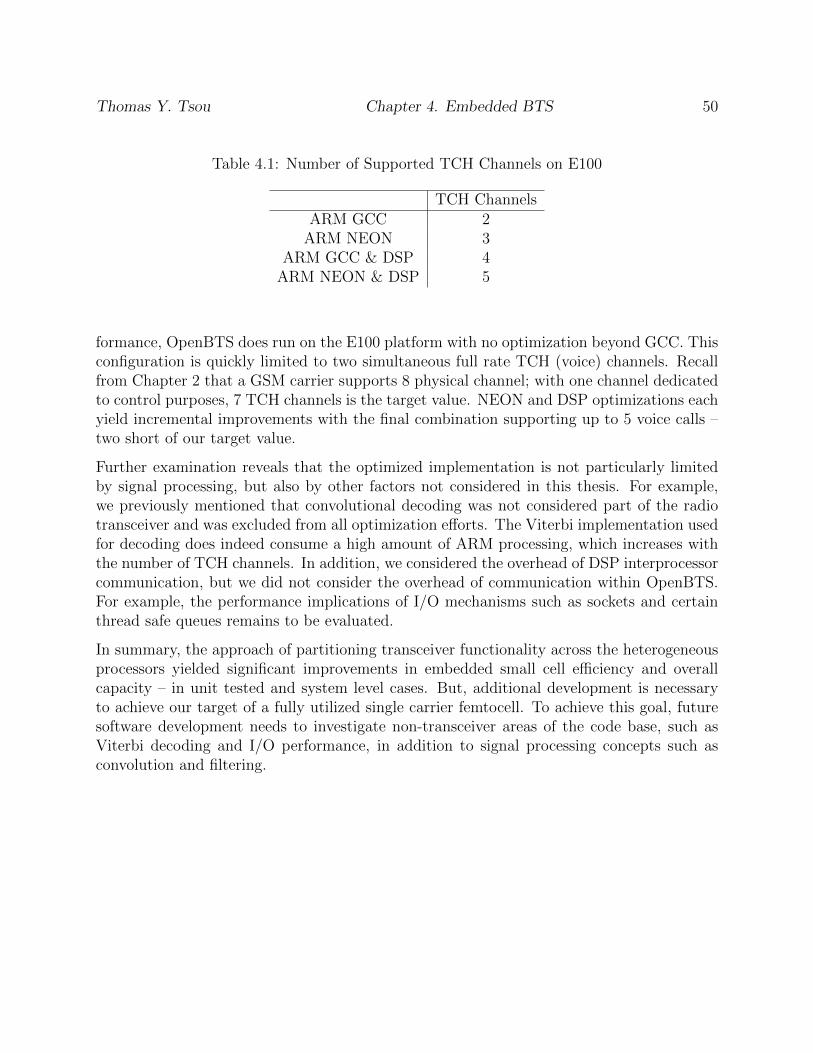
Thomas Y. Tsou Chapter 4. Embedded BTS 50
Table 4.1: Number of Supported TCH Channels on E100
TCH ChannelsARM GCC 2
ARM NEON 3ARM GCC & DSP 4
ARM NEON & DSP 5
formance, OpenBTS does run on the E100 platform with no optimization beyond GCC. Thisconfiguration is quickly limited to two simultaneous full rate TCH (voice) channels. Recallfrom Chapter 2 that a GSM carrier supports 8 physical channel; with one channel dedicatedto control purposes, 7 TCH channels is the target value. NEON and DSP optimizations eachyield incremental improvements with the final combination supporting up to 5 voice calls –two short of our target value.
Further examination reveals that the optimized implementation is not particularly limitedby signal processing, but also by other factors not considered in this thesis. For example,we previously mentioned that convolutional decoding was not considered part of the radiotransceiver and was excluded from all optimization efforts. The Viterbi implementation usedfor decoding does indeed consume a high amount of ARM processing, which increases withthe number of TCH channels. In addition, we considered the overhead of DSP interprocessorcommunication, but we did not consider the overhead of communication within OpenBTS.For example, the performance implications of I/O mechanisms such as sockets and certainthread safe queues remains to be evaluated.
In summary, the approach of partitioning transceiver functionality across the heterogeneousprocessors yielded significant improvements in embedded small cell efficiency and overallcapacity – in unit tested and system level cases. But, additional development is necessaryto achieve our target of a fully utilized single carrier femtocell. To achieve this goal, futuresoftware development needs to investigate non-transceiver areas of the code base, such asViterbi decoding and I/O performance, in addition to signal processing concepts such asconvolution and filtering.

Chapter 5
Concluding Remarks
Multicarrier and embedded GSM implementations were examined as the first and final topicsof this thesis respectively. In both cases the topics were considered independently, butthere is no fundamental restriction on combining the two development areas. Chapter 3showed that SIMD and DSP optimizations alone were insufficient for running a fully loadedOpenBTS configuration on one particular embedded platform. Looking forward, however,this limitation already has solutions.
The ARM Cortex-A8 processor was tested in this thesis, however, the successor processor isreadily available. With rapid processor advancements occurring in embedded, the Cortex-A9is a multicore processor with significantly higher performance in floating point efficiency,latency, and overall throughput than the A8 edition. Combined with an appropriate RFinterface, there is no doubt that such a configuration could serve as part of an effective futureSDR platform for higher performance embedded and multicarrier cellular implementations.
Further out on the horizon, advanced signal processing architectures with multiple DSPcores will provide larger increases in capabilities that are sufficient for not just multicarrierGSM, but multi-standard implementations as well. Chapter 2 introduced the concept ofextending multirate signal processing techniques to handle arbitrary signal bandwidths andchannel spacings. This level of system flexibility will become more and more relevant asfuture generation cellular technologies, such as LTE and LTE-Advanced, are deployed andoperated concurrently alongside existing networks. As these network combinations becomemore commonplace, in addition to use of heterogeneous small and large cells, the needfor reconfigurable components that can scale for capacity, radio technology, and operatingfrequency will only increase.
While this thesis examined multirate and embedded techniques in the scope of GSM systems,the topics discussed are extensible to new air interface technologies. Because of this appli-cability, the motivation for advancing the material in this thesis toward future multi-modesystems is very strong and serves as a topic worthy of future study.
51

Bibliography
[1] 3GPP, “Half Rate Speech Transcoding,” 3rd Generation Partnership Project (3GPP),TS 06.20, Nov. 2000.
[2] ——, “Physical layer on the radio path; General description,” 3rd Generation Partner-ship Project (3GPP), TS 45.001, Sep. 2008.
[3] ——, “Radio transmission and reception,” 3rd Generation Partnership Project (3GPP),TS 45.005, Sep. 2008.
[4] M. Saily, G. Sebire, E. Riddington, GSM/Edge: Evolution and Performance. Wiley,2011.
[5] R. Crochiere and L. Rabiner, Multirate Digital Signal Processing. Englewood Cliffs,NJ: Prentice Hall, 1983.
[6] f. harris, Multirate Signal Processing for Communication Systems. Upper Saddle River,NJ: Prentice Hall, 2004.
[7] Intel, “Intel 64 and IA32 Architectures Software Development Manual,” TS, May 2012.
[8] 3GPP, “Modulation,” 3rd Generation Partnership Project (3GPP), TS 45.004, Sep.2008.
[9] J. Proakis, Digital Communications. McGraw-Hill, 1995.
[10] P. Laurent, “Exact and Approximate Construction of Digital Phase Modulations bySuperposition of Amplitude Modulated Pulses (AMP),” Communications, IEEE Trans-actions on, vol. 34, no. 2, pp. 150 – 160, Feb 1986.
[11] Gumstix, “Overo COMS,” [Online] Available: http://www.gumstix.com, April 2012.
[12] 3GPP, “Radio subsystem synchronization,” 3rd Generation Partnership Project(3GPP), TS 05.10, Sep. 2003.
[13] ARM, “ARM Architecture Reference Manual: ARMv7-A and ARMv7-R edition,” ARMDDI 0406C, 2011.
52

[14] ——, “Cortex-A8: Technical Reference Manual,” ARM DDI 0344D, 2090.
53