implementation of the twofish cipher using fpga devices
TRANSCRIPT
1
Implementation of the Twofish CipherUsing FPGA Devices
Pawel Chodowiec, Kris Gaj
[email protected], [email protected]
Technical ReportElectrical and Computer Engineering
George Mason University
July 1999

2
Implementation of the Twofish Cipher Using FPGA Devices
George Mason University
Pawel Chodowiec, Kris Gaj
Table of Contents
1 SHORT DESCRIPTION OF THE TWOFISH CIPHER ............................................................................ 3
2 ANALYSIS OF THE TWOFISH CIPHER MAIN COMPONENTS.......................................................... 7
2.1 FIXED ROTATIONS.................................................................................................................................... 72.2 ADDITIONS MODULO 2 (XOR).................................................................................................................. 72.3 ADDITIONS MODULO 232
ON 32-BIT LONG WORDS ...................................................................................... 72.4 KEY DEPENDENT S-BOXES........................................................................................................................ 72.5 THE MAXIMUM DISTANCE SEPARABLE MATRIX ........................................................................................ 82.6 THE PSEUDO-HADAMARD TRANSFORM .................................................................................................... 9
3 THE STRUCTURE OF THE TWOFISH CIPHER .................................................................................. 10
3.1 IMPLEMENTATION OF ENCRYPTION AND DECRYPTION.............................................................................. 103.2 IMPLEMENTATION OF THE KEY SCHEDULE ............................................................................................... 10
4 DESIGN OF THE CIPHER INTERFACE................................................................................................ 12
4.1 TWOFISH INTERFACE.............................................................................................................................. 124.1.1 Interface signals............................................................................................................................ 124.1.2 Addressing .................................................................................................................................... 134.1.3 Data and key flow.......................................................................................................................... 144.1.4 The transmission protocol.............................................................................................................. 154.1.5 Operation sequence performed by our device after start................................................................. 164.1.6 Operation sequence recommended for the host device.................................................................... 16
4.2 THE TWOFISH ROUND CIRCUIT ............................................................................................................... 17
5 THE RESULTS OF TWOFISH IMPLEMENTATION USING XILINX FPGA DEVICES ................... 18
5.1 IMPLEMENTED PARTS ............................................................................................................................. 195.2 IMPLEMENTATION OF TWOFISH COMPONENTS ......................................................................................... 19
5.2.1 q – permutation ............................................................................................................................. 195.2.2 MDS matrix................................................................................................................................... 205.2.3 PHT transform .............................................................................................................................. 205.2.4 Summary of main components implementations.............................................................................. 20
5.3 IMPLEMENTATION OF THE F-FUNCTION ................................................................................................... 205.4 IMPLEMENTATION OF THE FULLY FUNCTIONAL ENCRYPTING DEVICE ........................................................ 21
6 SUMMARY ................................................................................................................................................ 22
7 BIBLIOGRAPHY....................................................................................................................................... 23
APPENDIX - LIST OF SOURCE FILES.......................................................................................................... 24
3
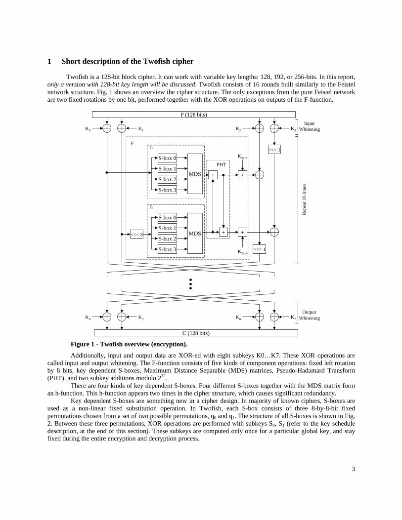
1 Short description of the Twofish cipher
Twofish is a 128-bit block cipher. It can work with variable key lengths: 128, 192, or 256-bits. In this report,only a version with 128-bit key length will be discussed. Twofish consists of 16 rounds built similarly to the Feistelnetwork structure. Fig. 1 shows an overview the cipher structure. The only exceptions from the pure Feistel networkare two fixed rotations by one bit, performed together with the XOR operations on outputs of the F-function.
P (128 bits)
+
+
+
+<<< 8
<<< 1
>>> 1
S-box 0
S-box 1
S-box 2
S-box 3
MDS
h
S-box 0
S-box 1
S-box 2
S-box 3
MDS
h
PHT
F
K2 K3K1K0
K2r+8
K2r+9
K6 K7K5K4
C (128 bits)
Rep
eat 1
6 tim
es
OutputWhitening
InputWhitening
Figure 1 - Twofish overview (encryption).
Additionally, input and output data are XOR-ed with eight subkeys K0…K7. These XOR operations arecalled input and output whitening. The F-function consists of five kinds of component operations: fixed left rotationby 8 bits, key dependent S-boxes, Maximum Distance Separable (MDS) matrices, Pseudo-Hadamard Transform(PHT), and two subkey additions modulo 232.
There are four kinds of key dependent S-boxes. Four different S-boxes together with the MDS matrix forman h-function. This h-function appears two times in the cipher structure, which causes significant redundancy.
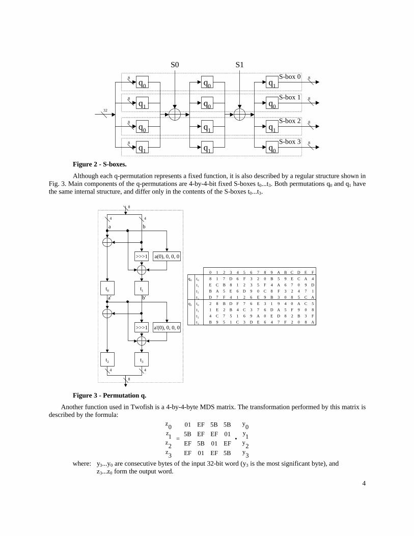
Key dependent S-boxes are something new in a cipher design. In majority of known ciphers, S-boxes areused as a non-linear fixed substitution operation. In Twofish, each S-box consists of three 8-by-8-bit fixedpermutations chosen from a set of two possible permutations, q0 and q1. The structure of all S-boxes is shown in Fig.2. Between these three permutations, XOR operations are performed with subkeys S0, S1 (refer to the key scheduledescription, at the end of this section). These subkeys are computed only once for a particular global key, and stayfixed during the entire encryption and decryption process.
4
q0
q1
q0
q1
q0
q0
q1
q1
q1
q0
q1
q0
S0 S1
S-box 0
S-box 1
S-box 2
S-box 3
8
8
8
8
32
8
8
8
8
Figure 2 - S-boxes.
Although each q-permutation represents a fixed function, it is also described by a regular structure shown inFig. 3. Main components of the q-permutations are 4-by-4-bit fixed S-boxes t0...t3. Both permutations q0 and q1 havethe same internal structure, and differ only in the contents of the S-boxes t0...t3.
>>>1
t0 t1
a(0), 0, 0, 0
>>>1
t2 t3
a'(0), 0, 0, 0
b'
a b
a'
4 4
44
A802F746ED3C159Bt
F3B28DE0A96157C4t
809F5AD673C4B2E1t
5CA04913E67FDB82tq
AC5803B9E6214F7Dt
17423F8C09D6E5ABt
D9076A4F53218BCEt
4ACE95B023F6D718tq
FEDCBA9876543210
3
2
1
01
3
2
1
00
8
8
Figure 3 - Permutation q.
Another function used in Twofish is a 4-by-4-byte MDS matrix. The transformation performed by this matrix isdescribed by the formula:
•
=
3y
2y
1y0
y
5BEF01EF
EF015BEF
01EFEF5B
5B5BEF01
3z2
z1
z0
z
where: y3...y0 are consecutive bytes of the input 32-bit word (y3 is the most significant byte), andz3...z0 form the output word.
5
This matrix multiplies a 32-bit input value by 8-bit constants, with all multiplications performed (byte bybyte) in the Galois field GF (28). The primitive polynomial is x8 + x6 + x5 + x3 + 1. Only three differentmultiplications are used effectively in the MDS matrix, namely multiplication
- by 5B16 = 0101 10112 (represented in GF(28) by a polynomial x6 + x4 + x3 + x + 1),- by EF16 = 1110 11112 (x
7 + x6 + x5 + x3 + x2 + x + 1), and- by 0116 = 0000 00012 (equivalent element in GF(28) is just 1) - obviously the result is equal to the input
value.
Finally, the PHT transform is a simple function that consists of two additions modulo 232, as shown in Fig.1. Results of the PHT transform can be described by the following equations:
a' = a + bb' = a + 2*b
Both additions are de facto independent and can be performed simultaneously.The nice feature of the Twofish algorithm is that, after little modifications, we can perform encryption and
decryption using exactly the same structure. It is very valuable for hardware implementations. Decryption requiresapplying subkeys in the reverse order and making a little modification to the main cipher structure as shown in Fig.4.
a)
<<< 1
>>> 1
F - function
b)
<<< 1
>>> 1
F - function
Figure 4 - Differences between the encryption and decryption a) encryption b) decryption.
Key schedule seems to be another strong side of the Twofish algorithm. There are two different sets ofsubkeys: S and K.
Two subkeys S0 and S1 are fixed during the entire encryption and decryption process. Both of them areobtained as a result of multiplying an appropriate part of a global key (128-bit wide, called M) by RS matrix. Thismatrix also performs multiplication in the Galois field GF (28), but the primitive polynomial is different then for thisMDS matrix: x8 + x6 + x3 + x2 + 1. The algorithm used to compute S keys is given by:
•
=
+
+
+
+
+
+
+
78i
68i
58i
48i
38i
28i
18i
8i
i,3
i,2
i,1
i,0
m
m
m
m
m
m
m
m
039EDB585A8755A4
193DAE47C1FCA102
E568C61EF38256A4
9EDB585A8755A401
s
s
s
s
where:- index i is from the range 0...1, and indicates the appropriate key S0 or S1,- si,3...si,0 are 8-bit parts of the 32-bit key Si (si,3 is the most significant byte),- m8i+7...m8i are 8-bit parts of the 128-bit user supplied key M.

6
Remaining set of subkeys K is computed in a structure very similar to that used for encryption. The onlydifference is that there is no key addition after the PHT transform, and that the fixed left rotation by 8 bits isperformed after instead of before the second h-function (compare Fig. 1 and Fig. 5). This feature enables computingsubkeys K using the same piece of hardware as the one used for encryption. The global key M is used toparameterize all key dependent S-boxes. All subkeys K are independent of each other, and are computed on thebasis of their index value. It means, that they can be computed on the fly in both directions: for encryption anddecryption.
q0
MDSq1
q0
q1
q0
q0
q1
q1
q1
q0
q1
q0
h
2i
2i
2i
2i
M2 M0
MDS
h
2i + 1M3 M1
2i + 1
2i + 1
2i + 1
+
+<<< 8 <<< 9
PHT K2i
K2i+1
q0
q1
q0
q1
q0
q0
q1
q1
q1
q0
q1
q0
Figure 5 - Generation of subkeys K.
Keys M3…M0, shown in Fig. 5, are derived directly from the main 128-bit key. They are just 32-bit parts ofthe main key, where M3 corresponds to the most significant 32 bits, and M0 to the least significant bits of M. Thesesubkeys are used to customize S-boxes, and stay fixed for all rounds.
The variable i is from range 0…19, and is used to generate a set of corresponding subkeys K0…K39.
7
2 Analysis of the Twofish cipher main components
The analysis presented in this section concerns the ability of implementing Twofish using Xilinx FPGAdevices.
In the following section, all basic functions used in Twofish, and the way of implementing them in XilinxFPGAs will be discussed. These basic functions include:
- fixed rotations- additions modulo 2 (bit by bit)- additions modulo 232 on 32-bit long words- key dependent S-boxes- MDS matrices- PHT transforms
2.1 Fixed rotations
This kind of operations is easily realizable in hardware. They do not even require any additional resources.The only thing we have to do is to reorder interconnections between logic cells.
2.2 Additions modulo 2 (XOR)
This is a second very inexpensive and fast operation. Each output bit depends on value of only two inputbits. It is obvious that such operation can be done using only a single F or G lookup table in Xilinx FPGA.Therefore, one CLB can be used to compute this function on two bits. For example, XOR on two 32-bit long wordsrequires only 16 logic cells. Besides, each XOR uses only two inputs, but there are four inputs available in eachlookup table. As a result, in many cases, XOR can be combined with other operations and implemented in the samecell.
2.3 Additions modulo 232 on 32-bit long words
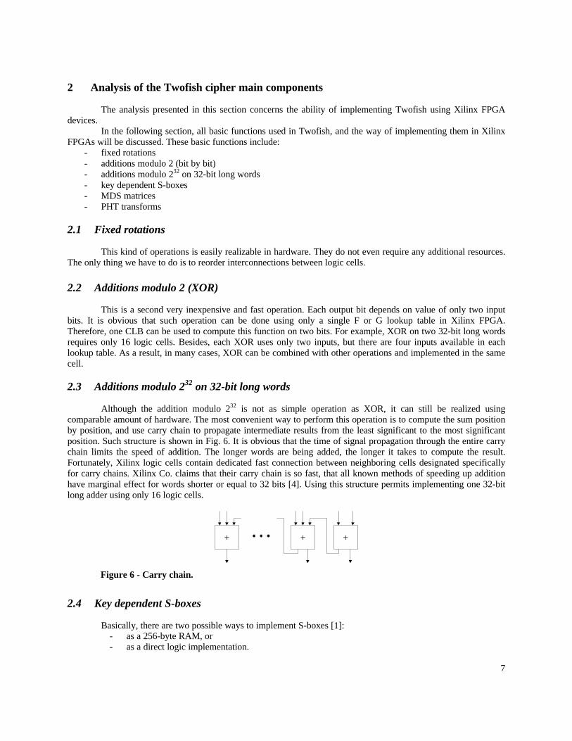
Although the addition modulo 232 is not as simple operation as XOR, it can still be realized usingcomparable amount of hardware. The most convenient way to perform this operation is to compute the sum positionby position, and use carry chain to propagate intermediate results from the least significant to the most significantposition. Such structure is shown in Fig. 6. It is obvious that the time of signal propagation through the entire carrychain limits the speed of addition. The longer words are being added, the longer it takes to compute the result.Fortunately, Xilinx logic cells contain dedicated fast connection between neighboring cells designated specificallyfor carry chains. Xilinx Co. claims that their carry chain is so fast, that all known methods of speeding up additionhave marginal effect for words shorter or equal to 32 bits [4]. Using this structure permits implementing one 32-bitlong adder using only 16 logic cells.
+++
Figure 6 - Carry chain.
2.4 Key dependent S-boxes
Basically, there are two possible ways to implement S-boxes [1]:- as a 256-byte RAM, or- as a direct logic implementation.

8
First type of design would require eight 256-byte memories. Xilinx FPGA devices do not contain any dedicatedRAM and thus a 256-byte RAM would have to be implemented using logic cells. Each CLB can be configured as 16x 2 bit RAM memory [4]. Therefore, 512 (8 * (256 x 8) / (16 x 2)) logic cells are needed to implement all eight S-boxes, which is a large number. Additionally, the access time to this memory would be long. However, such solutioncan still be taken into account in case of the Altera FPGA devices, where additional RAM elements (EAB) exist.Additional drawback of this method is a long time of key exchange, because the contents of all memory cells have tobe precomputed, based on the current key.
In a second type of design, we have a degree of freedom. First of all, each q-permutation can beimplemented as a 256-byte ROM, or as a logic function (see Fig. 3). Although, there are only two differentpermutations, they are used simultaneously in eight S-boxes. It is obvious, that this kind of implementation alsorequires too many logic cells in Xilinx FPGA, and it will not work faster than the direct logic implementation.Hence, let us consider only the direct logic implementation. As shown in Fig. 3, each q-permutation consists of four4-by-4-bit S-boxes t0...t3, and some additional logic. Since each of these little S-boxes forms only a four-bit inputfunction, it can be easily realized using only two parallel CLBs. In other words, the delay caused by one S-box t isequal to the delay of a single CLB. Remaining operations in the permutation q are easy to implement using twolevels of logic cells. In summary, each q-permutation can be implemented using 16 CLBs arranged in a four levelstructure.
Taking into account our calculations for q-permutations, each S-box S0...S3 should take 56 logic cells (3 *16 CLBs for each q-permutation + 8 CLBs for XOR with fixed keys S0 and S1). However, its structure consists of 14levels of logic cells (3 q-perm. * 4 levels per each permutation + 2 XORs * 1 level per each XOR). It means thatcomputation can consume a lot of time. Fortunately, each S-box can be easily divided into several logic layers usingregisters, so that we can still use fast clock rate.
2.5 The Maximum Distance Separable matrix
Implementation of the MDS matrix can seem very difficult, but closer analysis of operations performed inthis matrix leads us to a different conclusion. As it was shown in section 1, there are only two differentmultiplications that require to be implemented. In case of multiplication by 5B16, every output depends on at mostfour inputs. Therefore, this multiplication consumes only four parallel CLBs – see Fig. 7a.
a)x7 x1
y7
x7 x5 x1
y5
x6 x4 x1 x0
y4
x5 x3 x0
y3
x4 x2 x1
y2
x3 x1 x0
y1
x2 x0
y0
x6 x0
y6
CLB 1 CLB 2 CLB 3 CLB 4
b)x7 x1
y7
x7 x6 x1
y5
x6 x5 x1
y4
x5 x4 x0
y3
x3 x2 x0
y1
x2 x0
y0
x6 x0
y6
CLB 1 CLB 2 CLB 3 CLB 5
x5 x0 x4 x3 x1
y2
CLB 4
x2 x0x0 x7 x4 x3 x1 x1
Figure 7 – Multiplication by a constant in the GF(28)a) Multiplication by 5B16 ≡≡ x6 + x4 + x3 + x + 1b) Multiplication by EF16 ≡≡ x7 + x6 + x5 + x3 + x2 + x + 1

9
The multiplication by EF16 contains two outputs depending on five input bits. These outputs require anentire CLB each, therefore the entire multiplication will take five parallel CLBs. Nevertheless, any multiplication inGF(28) can be implemented using up to eight parallel CLBs. As a result, the time of a single multiplication is equalto the delay of one CLB.
The results of all multiplications in each row of the MDS matrix are finally XOR-ed bit by bit. Suchoperation needs only four CLBs for each row. To compute one byte of the result, it is necessary to perform onlythree multiplications. Thus, we need only 17-18 logic cells (4-5 CLBs per multiplication * 3 multiplications + 4CLBs for XOR). All CLBs are organized in a two level structure, allowing computing results in a very high speed.The entire MDS matrix implementation can fit in 52 cells. This number of cells results from the fact that there aretwo identical multiplication factors in each column of the MDS matrix (see section 1), and the correspondingmultiplication operation need to be performed only once. 52 = (4 columns * (4 + 5 CLBs required for bothmultiplications in the column) + 16 CLBs for final addition).
2.6 The Pseudo-Hadamard Transform
The PHT transform is composed of two additions. It was shown in section 1 that both additions can beperformed in parallel. The only additional operation is one left shift by one bit, as shown in Fig. 8. Obviously, bothadditions are implemented in the same way as ordinary addition modulo 232, discussed in section 2.3.
+
<< 1
+
Figure 8 - The PHT after changes.
10
3 The structure of the Twofish cipher
The Twofish cipher can be implemented in many ways. Each of these ways can be better or worsedepending on particular requirements. In the following section, we would like to discuss some of the possiblealternative methods of implementing Twofish.
3.1 Implementation of encryption and decryption
First of all we can choose between implementing the cipher using purely combinational design (notcounting the main register required to store a final result of each round), and using sequential design with registersdividing the combinational logic into smaller but faster blocks.
First kind of design is probably the fastest, but also hard to optimize for minimum area, because functionsharing is difficult to apply. Additionally, a combinational design may work only with a very low clock frequency,and its synthesis may be significantly longer. The speed of the sequential design is lower, because we are not able todivide the circuit into exactly equal blocks, and this way we lose precious nanoseconds. On the other hand, in manycases, a sequential design allows time sharing of the same part of the circuit between various functions, which cansignificantly reduce the amount of area consumed by this design. Moreover, in the ECB mode of the block cipher (aswell as in more complex interleaved modes), the sequential design may increase the encryption speed directlyproportionally to the number of pipelined stages.
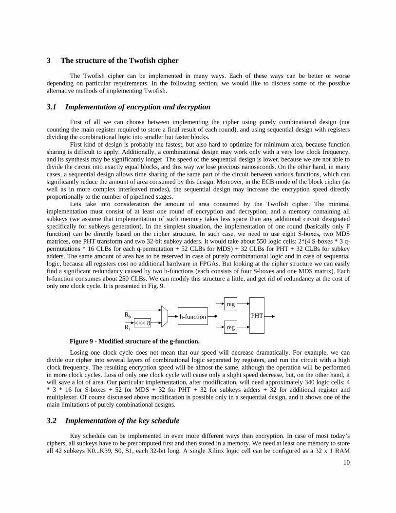
Lets take into consideration the amount of area consumed by the Twofish cipher. The minimalimplementation must consist of at least one round of encryption and decryption, and a memory containing allsubkeys (we assume that implementation of such memory takes less space than any additional circuit designatedspecifically for subkeys generation). In the simplest situation, the implementation of one round (basically only Ffunction) can be directly based on the cipher structure. In such case, we need to use eight S-boxes, two MDSmatrices, one PHT transform and two 32-bit subkey adders. It would take about 550 logic cells: 2*(4 S-boxes * 3 q-permutations * 16 CLBs for each q-permutation + 52 CLBs for MDS) + 32 CLBs for PHT + 32 CLBs for subkeyadders. The same amount of area has to be reserved in case of purely combinational logic and in case of sequentiallogic, because all registers cost no additional hardware in FPGAs. But looking at the cipher structure we can easilyfind a significant redundancy caused by two h-functions (each consists of four S-boxes and one MDS matrix). Eachh-function consumes about 250 CLBs. We can modify this structure a little, and get rid of redundancy at the cost ofonly one clock cycle. It is presented in Fig. 9.
h-function<<< 8
reg
reg
PHTR0
R1
Figure 9 - Modified structure of the g-function.
Losing one clock cycle does not mean that our speed will decrease dramatically. For example, we candivide our cipher into several layers of combinational logic separated by registers, and run the circuit with a highclock frequency. The resulting encryption speed will be almost the same, although the operation will be performedin more clock cycles. Loss of only one clock cycle will cause only a slight speed decrease, but, on the other hand, itwill save a lot of area. Our particular implementation, after modification, will need approximately 340 logic cells: 4* 3 * 16 for S-boxes + 52 for MDS + 32 for PHT + 32 for subkeys adders + 32 for additional register andmultiplexer. Of course discussed above modification is possible only in a sequential design, and it shows one of themain limitations of purely combinational designs.
3.2 Implementation of the key schedule
Key schedule can be implemented in even more different ways than encryption. In case of most today’sciphers, all subkeys have to be precomputed first and then stored in a memory. We need at least one memory to storeall 42 subkeys K0...K39, S0, S1, each 32-bit long. A single Xilinx logic cell can be configured as a 32 x 1 RAM

11
memory, so that to store all subkeys, we would have to use at least 42 / 32 * (32 x 1) = 64 CLBs. For greaterconvenience, we would actually need three 32-bit memories, one for whitening subkeys, and two others for the restof subkeys K, where odd and even keys are kept in separate memories. Each of these memories will store maximum16 subkeys. In such case, a single CLB can be configured as a 16 x 2 RAM memory, and it is sufficient to use only48 of CLBs for all subkeys K.
Much more inconvenient are subkeys S0 and S1. They cannot be stored in any of the above memories,because they are used simultaneously with the other sybkeys. Moreover, even both keys S cannot be stored togetherif the cipher round is implemented as a purely combinational logic. Therefore, storing of these subkeys consumesadditional 32 CLBs.
The computation of internal keys can be done either on-chip or off-chip. If it is performed on-chip, we haveto provide additional block of hardware designated only for this operation. Fortunately, in Twofish, the circuit usedfor subkey generation is very similar to the one used for encryption. After some little modifications, the same blockof hardware can be used for both encryption and key scheduling. The only part of key scheduling that still requiresdistinct hardware is RS matrix. So far, we did not analyze this matrix and we cannot say how much area it is goingto take.
The other possibility is to precompute all subkeys outside of the circuit, and then download them into thecircuit memory. This method requires implementing only a memory, but is less convenient, and may affect thesecurity of the implementation.
The main drawback of both methods is a long time of key exchange. In some applications it may berequired to change keys very often, and this time may become critical.
To minimize the time of key exchange, the subkeys can be computed on the fly. In case of Twofish, it isrelatively easy, because all subkeys are independent of each other. As a result, the key exchange time is limited onlyby the time of performing multiplication by RS matrix. But nothing comes for free. We have to design additionallogic to perform subkeys computation simultaneously with encryption. The straightforward implementation of thisfunction will double the size of the circuit. However, it seems to be possible to compute all subkeys on the fly in thesame circuit as encryption by using time sharing. So far, we did not investigate the time penalty inferred by thisoption.
12
4 Design of the cipher interface
Our project is divided into two distinct parts: Twofish round circuit and external interface. The roundcircuit describes exactly one round of the Twofish cipher, including encryption and decryption. The round can berun repeatedly to perform entire encryption or decryption process. Our design does not include a key scheduleimplementation, because we assumed that the speed of key scheduling has a secondary influence on results ofcomparison of different ciphers. However, the Twofish key schedule is very similar to encryption, and seems to beone of the strong points of this cipher. Therefore, we do not exclude its implementation in the future. In presentimplementation, all subkeys have to be computed off-chip and then written to the appropriate on-chip memories andregisters.
4.1 Twofish interface
External interface is of our own invention, and should not be taken into account during comparison ofefficiency of various ciphers. Our purpose was to create a general-purpose interface, which will be very easy tooperate in a microprocessor system, and will allow performing encryption with the maximum speed, using anarbitrary AES candidate cipher.
4.1.1 Interface signals
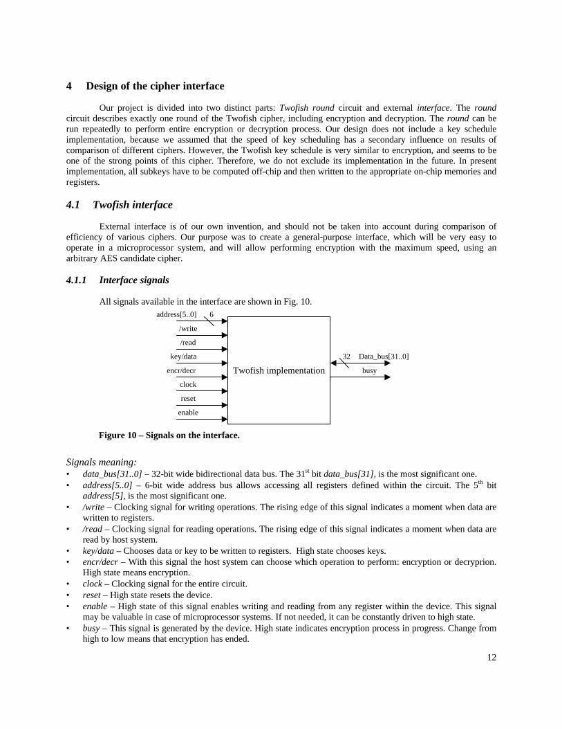
All signals available in the interface are shown in Fig. 10.
Data_bus[31..0]
/write
/read
clock
reset
key/data
encr/decr
address[5..0]
busyTwofish implementation
6
32
enable
Figure 10 – Signals on the interface.
Signals meaning:• data_bus[31..0] – 32-bit wide bidirectional data bus. The 31st bit data_bus[31], is the most significant one.• address[5..0] – 6-bit wide address bus allows accessing all registers defined within the circuit. The 5th bit
address[5], is the most significant one.• /write – Clocking signal for writing operations. The rising edge of this signal indicates a moment when data are
written to registers.• /read – Clocking signal for reading operations. The rising edge of this signal indicates a moment when data are
read by host system.• key/data – Chooses data or key to be written to registers. High state chooses keys.• encr/decr – With this signal the host system can choose which operation to perform: encryption or decryprion.
High state means encryption.• clock – Clocking signal for the entire circuit.• reset – High state resets the device.• enable – High state of this signal enables writing and reading from any register within the device. This signal
may be valuable in case of microprocessor systems. If not needed, it can be constantly driven to high state.• busy – This signal is generated by the device. High state indicates encryption process in progress. Change from
high to low means that encryption has ended.
13
4.1.2 Addressing
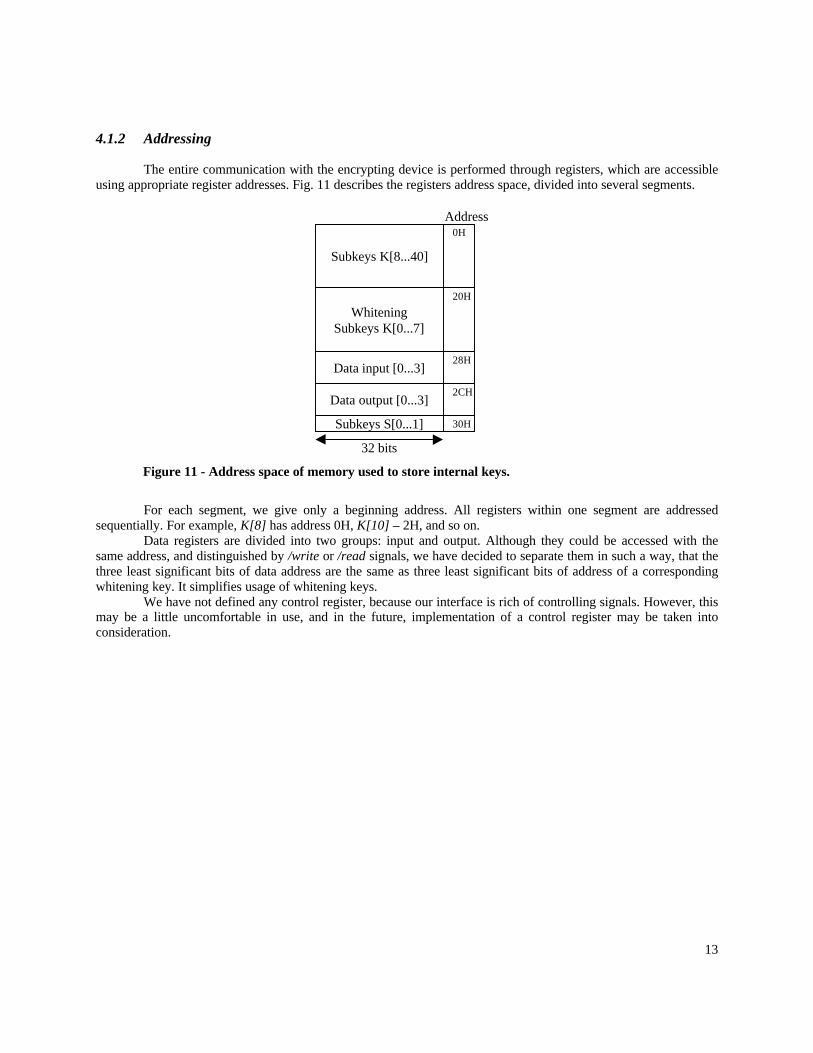
The entire communication with the encrypting device is performed through registers, which are accessibleusing appropriate register addresses. Fig. 11 describes the registers address space, divided into several segments.
0H
20H
28H
2CH
30H
Subkeys K[8...40]
WhiteningSubkeys K[0...7]
Data input [0...3]
Data output [0...3]
Subkeys S[0...1]
Address
32 bits
Figure 11 - Address space of memory used to store internal keys.
For each segment, we give only a beginning address. All registers within one segment are addressedsequentially. For example, K[8] has address 0H, K[10] – 2H, and so on.
Data registers are divided into two groups: input and output. Although they could be accessed with thesame address, and distinguished by /write or /read signals, we have decided to separate them in such a way, that thethree least significant bits of data address are the same as three least significant bits of address of a correspondingwhitening key. It simplifies usage of whitening keys.
We have not defined any control register, because our interface is rich of controlling signals. However, thismay be a little uncomfortable in use, and in the future, implementation of a control register may be taken intoconsideration.
14
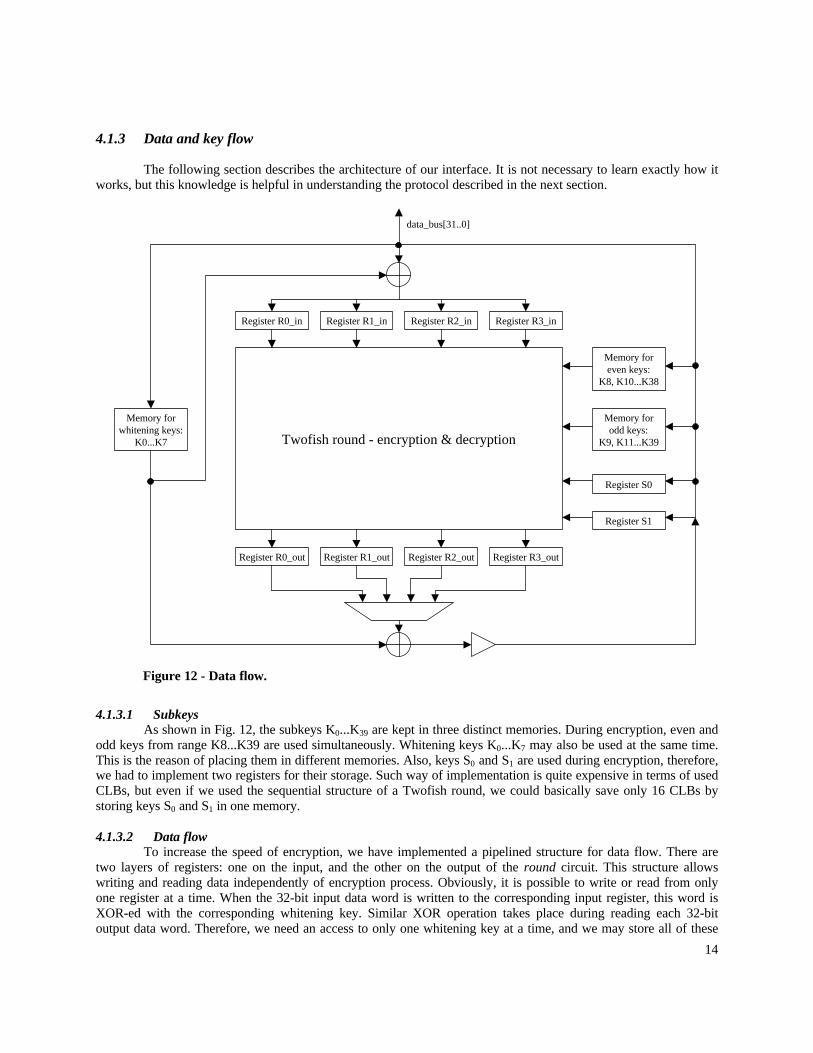
4.1.3 Data and key flow
The following section describes the architecture of our interface. It is not necessary to learn exactly how itworks, but this knowledge is helpful in understanding the protocol described in the next section.
Twofish round - encryption & decryption
Memory forodd keys:
K9, K11...K39
Memory foreven keys:
K8, K10...K38
Memory forwhitening keys:
K0...K7
Register S0
Register S1
Register R0_in Register R1_in Register R2_in Register R3_in
Register R0_out Register R1_out Register R2_out Register R3_out
data_bus[31..0]
Figure 12 - Data flow.
4.1.3.1 SubkeysAs shown in Fig. 12, the subkeys K0...K39 are kept in three distinct memories. During encryption, even and
odd keys from range K8...K39 are used simultaneously. Whitening keys K0...K7 may also be used at the same time.This is the reason of placing them in different memories. Also, keys S0 and S1 are used during encryption, therefore,we had to implement two registers for their storage. Such way of implementation is quite expensive in terms of usedCLBs, but even if we used the sequential structure of a Twofish round, we could basically save only 16 CLBs bystoring keys S0 and S1 in one memory.
4.1.3.2 Data flowTo increase the speed of encryption, we have implemented a pipelined structure for data flow. There are
two layers of registers: one on the input, and the other on the output of the round circuit. This structure allowswriting and reading data independently of encryption process. Obviously, it is possible to write or read from onlyone register at a time. When the 32-bit input data word is written to the corresponding input register, this word isXOR-ed with the corresponding whitening key. Similar XOR operation takes place during reading each 32-bitoutput data word. Therefore, we need an access to only one whitening key at a time, and we may store all of these
15
keys in a common memory. Input and output whitening keys have to be exchanged during decryption. It requiressetting properly the encr/decr signal during the data transmission. Whitening keys are applied to the input data onthe fly, which is a little unusual, and may increase the minimum time of the transmission cycle.
NOTE: Interface implementation for other ciphersWe are going to use the same basic interface structure for all ciphers. Of course, for each cipher we will
customize this structure according to the specific conditions, nevertheless, our interface will always include at leastthe following features:
1) Data and keys will be read and written through 32-bit wide bidirectional bus.2) We will always use pipelined structure for data flow.3) All subkeys will be computed off-chip, and stored in internal memories in such a way, that all subkeys
required during a single round will be available simultaneously within one clock cycle.
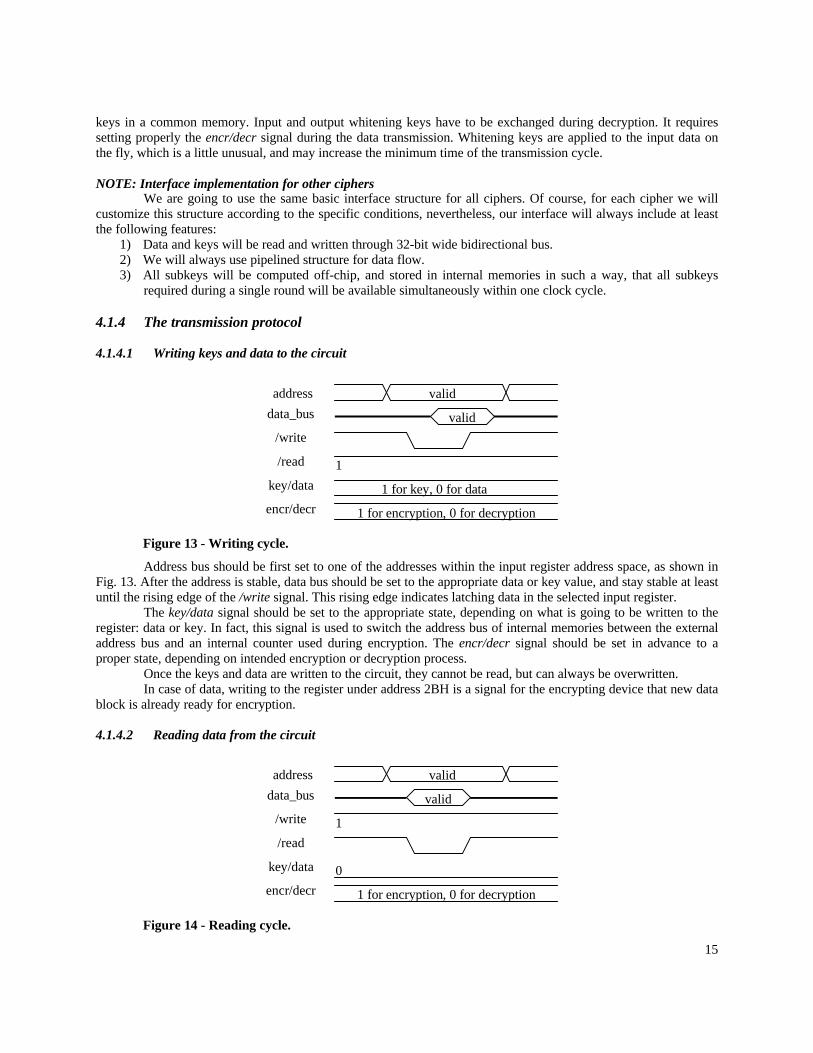
4.1.4 The transmission protocol
4.1.4.1 Writing keys and data to the circuit
address
data_bus
/write
/read
key/data
encr/decr
valid
valid
1 for key, 0 for data
1 for encryption, 0 for decryption
1
Figure 13 - Writing cycle.
Address bus should be first set to one of the addresses within the input register address space, as shown inFig. 13. After the address is stable, data bus should be set to the appropriate data or key value, and stay stable at leastuntil the rising edge of the /write signal. This rising edge indicates latching data in the selected input register.
The key/data signal should be set to the appropriate state, depending on what is going to be written to theregister: data or key. In fact, this signal is used to switch the address bus of internal memories between the externaladdress bus and an internal counter used during encryption. The encr/decr signal should be set in advance to aproper state, depending on intended encryption or decryption process.
Once the keys and data are written to the circuit, they cannot be read, but can always be overwritten.In case of data, writing to the register under address 2BH is a signal for the encrypting device that new data
block is already ready for encryption.
4.1.4.2 Reading data from the circuit
address
data_bus
/write
/read
key/data
encr/decr
valid
valid
0
1 for encryption, 0 for decryption
1
Figure 14 - Reading cycle.

16
Reading data is very similar to writing. Instead of /write, a /read signal is used to indicate reading cycle. Ofcourse, this time the encryption device drives data on the data_bus, therefore a host system should release the bus.Data are driven on the data_bus as long as /read signal stays low.
4.1.5 Operation sequence performed by our device after start
The key to use the device efficiently is to understand what operations are performed after start signalactivation. This sequence is very simple:
1) Read data from input registers and store them inside the circuit round, set busy = 12) Perform encryption3) Write encrypted data to output registers, and set busy = 0
There are two important conclusions, which should be taken into consideration:1) Immediately after the busy signal becomes high the host may write next data.2) When busy becomes low, encrypted data are available to read. It is important to notice that our device does
not wait for a host system, and previously encrypted data should be already read at the end of the nextencryption, otherwise they will be lost.
4.1.6 Operation sequence recommended for the host device
The pipelined structure used in our interface makes writing and reading data possible during processingencryption. The sequence of operations looks as follows:
1) Write data
2) Write next data3) Wait for busy = 04) Read encrypted data5) Go to step 2.
17
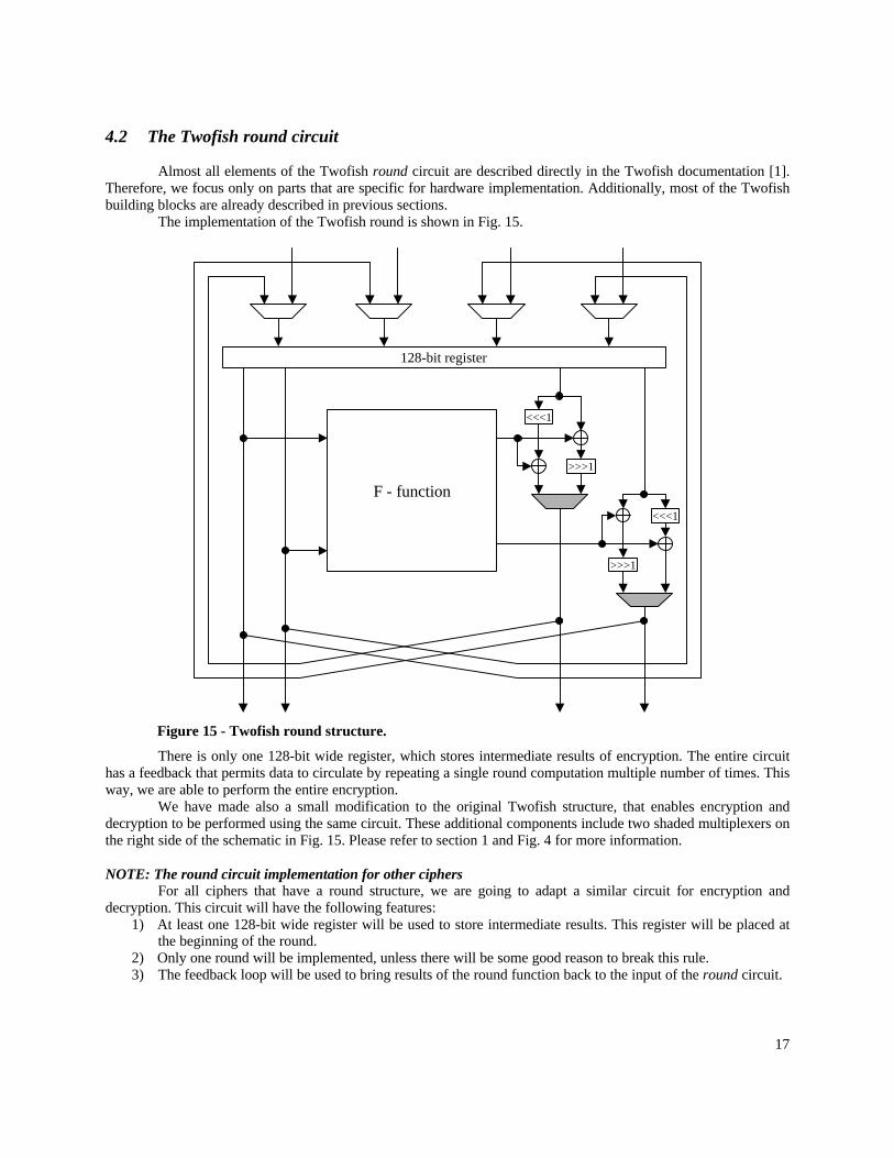
4.2 The Twofish round circuit
Almost all elements of the Twofish round circuit are described directly in the Twofish documentation [1].Therefore, we focus only on parts that are specific for hardware implementation. Additionally, most of the Twofishbuilding blocks are already described in previous sections.
The implementation of the Twofish round is shown in Fig. 15.
128-bit register
F - function
<<<1
>>>1
<<<1
>>>1
Figure 15 - Twofish round structure.
There is only one 128-bit wide register, which stores intermediate results of encryption. The entire circuithas a feedback that permits data to circulate by repeating a single round computation multiple number of times. Thisway, we are able to perform the entire encryption.
We have made also a small modification to the original Twofish structure, that enables encryption anddecryption to be performed using the same circuit. These additional components include two shaded multiplexers onthe right side of the schematic in Fig. 15. Please refer to section 1 and Fig. 4 for more information.
NOTE: The round circuit implementation for other ciphersFor all ciphers that have a round structure, we are going to adapt a similar circuit for encryption and
decryption. This circuit will have the following features:1) At least one 128-bit wide register will be used to store intermediate results. This register will be placed at
the beginning of the round.2) Only one round will be implemented, unless there will be some good reason to break this rule.3) The feedback loop will be used to bring results of the round function back to the input of the round circuit.

18
5 The results of the Twofish implementation using Xilinx FPGA devices
VHDL (Very High Speed Integrated Circuit Hardware Description Language) was chosen as a languageused to describe Twofish implementation. VHDL is a standard language for hardware description and is supportedby computer aided design software of all major FPGA device vendors. It is a high-level language, which allowsdescribing circuit function without the need to specify the circuit structure. Although writing the VHDL code is veryeasy, it is not guaranteed that this code will be optimal. The results substantially depend on the software used forsynthesis. Additionally, different ways of describing the same circuit produce slightly different results. Therefore,writing a good code requires an in-depth knowledge of how VHDL is interpreted by a synthesizer. To optimize theimplementation, we have tried different kinds of description, and compared the results with our expectations (seesection 2).
Probably, the best way to write the most efficient code is to use vendor supported libraries. However, thisway of coding would make our design specific for a particular device family. Therefore, we have described theentire round circuit, which is the core of our design, in pure VHDL’87 language. We expect that using library partscould make our design faster and less area consuming. In the interface part, we have made an exception and usedlibrary parts from the Xilinx LogiBLOX library. These library parts were necessary to describe memories used tostore cipher subkeys. Any other way of implementing these memories would dramatically increase the amount ofrequired area.
The majority of the designer’s time has been spent on creating the proper VHDL code, and on functionalsimulation. We did it using mainly the Active-VHDL program provided by ALDEC Co. We have found thisprogram very convenient to work with VHDL, and to perform functional simulation. Our code was verified based ontest vectors provided in Twofish documentation [1]. The verified VHDL code was then synthesized and optimizedusing FPGA Express. The obtained netlist was exported to the Xilinx Foundation Series 1.5 to create theimplementation. The Xilinx design environment was also used for timing simulation.
As target device we have chosen a family of XC4000XL. In most implementations, we have used thefollowing options:
In FPGA Express:• Clock frequency: 50 MHz• Speed grade: -09• Slew rate: Slow• Global buffer: Automatic, but in case of clock and reset signals: BUFGLS• Hierarchy: Eliminate, but in case of subkey memories: Preserve• Primitives: Optimize• Operator Sharing: On• Optimize for: Speed• Effort: High
In Design Manager:• Trim unconnected logic: on• Replace logic to allow logic level reduction: on• Generate 5-input functions: on• CLB packing strategy: Fit device• Pack CLB for: Structure• Pack I/O registers/latches into IOBs: off• Place & route effort level: Best result• # of routing passes: auto• # of delay-based cleanup passes: 0
19
5.1 Implemented parts
After analyzing all Twofish components in terms of their ability to be implemented in Xilinx FPGAdevices, as described in section 2, we also tried to verify whether our expectations are fulfilled or even exceeded byXilinx synthesis tools. Implemented parts included:
• q-permutations• the MDS matrix• the PHT transform• the F-function• full encrypting device in combinational version
5.2 Implementation of Twofish components
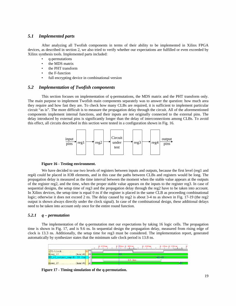
This section focuses on implementation of q-permutations, the MDS matrix and the PHT transform only.The main purpose to implement Twofish main components separately was to answer the question: how much areathey require and how fast they are. To check how many CLBs are required, it is sufficient to implement particularcircuit “as is”. The more difficult is to measure the propagation delay through the circuit. All of the aforementionedcomponents implement internal functions, and their inputs are not originally connected to the external pins. Thedelay introduced by external pins is significantly longer than the delay of interconnections among CLBs. To avoidthis effect, all circuits described in this section were tested in a configuration shown in Fig. 16.
reg1 reg2Circuitundertest
reg3 reg4inputpins
outputpins
Figure 16 - Testing environment.
We have decided to use two levels of registers between inputs and outputs, because the first level (reg1 andreg4) could be placed in IOB elements, and in this case the paths between CLBs and registers would be long. Thepropagation delay is measured as the time interval between the moment when the stable value appears at the outputsof the register reg2, and the time, when the proper stable value appears on the inputs to the register reg3. In case ofsequential designs, the setup time of reg3 and the propagation delay through the reg2 have to be taken into account.In Xilinx devices, the setup time is equal 0 ns if the register is placed in the same CLB as proceeding combinationallogic; otherwise it does not exceed 2 ns. The delay caused by reg2 is about 3-4 ns as shown in Fig. 17-19 (the reg2output is shown always directly under the clock signal). In case of the combinational design, these additional delaysneed to be taken into account only once for the entire round function.
5.2.1 q – permutation
The implementation of the q-permutation met our expectations by taking 16 logic cells. The propagationtime is shown in Fig. 17, and is 9.6 ns. In sequential design the propagation delay, measured from rising edge ofclock is 13.3 ns. Additionally, the setup time for reg3 must be considered. The implementation report, generatedautomatically by synthesizer states that the minimum safe clock period is 13.8 ns.
Figure 17 - Timing simulation of the q-permutation.

20
5.2.2 MDS matrix
In case of the MDS matrix implementation, the Xilinx compiler made it in a completely different way thatwe had expected. Our analysis shows that it should be the fastest function, but in implementation it appeared to benot much faster than the q-permutation, causing the delay of 9.5 ns (13.5 ns with the reg2 propagation delay). Thecompiler realized it using only 48 logic cells (we expected 52), but, on the other hand, it has changed it into amultilevel structure. We tried several different ways of describing this matrix, but the result still was the same.Probably, the only way to enforce our implementation would be to use library components.
Figure 18 - Timing simulation of the MDS matrix.
5.2.3 PHT transform
The PHT transform was implemented using carry-chain feature of Xilinx CLBs, and it took 34 CLBs. Weexpected a long delay that is needed for the signal propagation through the entire carry-chain, but Xilinx FPGAseems to be very fast, and it took only 6.8 ns (10.8 ns, taking into account propagation delay through the reg2).Surprisingly, the minimum clock period reported by the synthesizer is 14.7 ns.
Figure 19 - Timing simulation of the PHT transform.
5.2.4 Summary of main components implementations
q-permutation MDS PHTExpected delay(# of CLB levels)
4 2 carry-chain
Actual delay (ns) 9.6* 13.3** 9.5* 13.5** 6.8* 10.8**Expected size (# CLBs) 16 52 32Actual size (# CLBs) 16 48 34
* with the propagation time through reg2** without the propagation time through reg2
5.3 Implementation of the F-function and full round
The F-function is a core part of the entire round circuit, and it determines the encryption speed. Moreover,the key schedule is based on the same function. Therefore, the amount of area consumed by the full implementationof Twofish can be estimated as twice the area of the F-function implementation. This estimate does not take intoaccount the amount of area used by the RS matrix.
We have implemented two versions of the F-function: sequential and fully combinational. Both versions ofF-functions were used for implementation of the round circuit. In the sequential version, we used six register layerssituated at the outputs of the:
• 1st level of q-permutations,• 2nd level of q-permutations,• 3rd level of q-permutations,

21
• MDS matrix,• PHT transform,• subkey adders.
For the combinational version of the F-function, the required amount of CLBs is 605, which matchesperfectly with our expectations. The corresponding entire round function implementation takes 705 logic cells. Thesequential version of the F-function takes 613 CLBs, and the entire round implementation fits in 728 logic cells.
5.4 Implementation of the fully functional encrypting device
The implementation of the Twofish encrypting device consists of the round function and the interfacedescribed in section 4. We have implemented a purely combinational and a sequential version of the entire circuit,with different optimization options. The smallest device that contains the entire circuit is XC4028XL. As a targetpackage for this device we used HQ208.
Version Combinational SequentialOptimized for Speed Area Speed AreaRouting* Best Default Best Default Best Default Best DefaultSize (# CLBs) 911 888 920 926Max. clock rate (MHz) 10.7 9.1 10.6 9.1 33 28.5 35.9** 27.9# of clock cycles per data block 16 112Maximum throughput (Mbit/s) 85.6 72.8 84.8 72.8 37.7 32.6 41.0 31.9
* Best: # of routing passes: 1000# of delay-based cleanup passes: 5
Default: options are set as listed in section 5.** This is the most surprising result, but we have checked all options and we are certain that the
optimizations for speed and area were not interchanged.
As we expected, the combinational version of the implementation is faster than the sequential version. Thethroughput of the sequential implementation is surprisingly low. According to the results obtained for individualTwofish components, we have expected the maximum clock rate at a level of 50 MHz. Actually, the clock rate didnot exceed the rate of 36 MHz, resulting in the throughput lower by 50% compared to the combinational version. Itmay be the result of poor routing, because the design takes approximately 90% of area available in the XC4028device.
Although, the sequential implementation is slower, it may be still considered in case of the ECB ciphermode or interleaved modes, because, for these modes, the computations can be performed for many data blockssimultaneously. Obviously, this solution requires implementing additional FIFO buffers instead of registers at theinput and output of the circuit, and one similar FIFO buffer on the left half of the data inside the round.Implementing these buffers using flip-flops would be very expensive, but instead, we can use the fact that a XilinxCLB can be configured as a 16 x 1 dual-port RAM. Therefore, each required 32-bit-wide FIFO buffer would takeonly 32 logic cells. Using pipelined mode for our particular sequential design (seven levels of registers), would givethe throughput of 263.9 Mbit/s. One FIFO buffer can store up to 16 data blocks, therefore, the throughput may befurther increased by dividing the circuit into more register levels. This operation does not require any additionalhardware.

22
Summary
We have designed the hardware implementation of Twofish, one of the leading candidates to the newAdvanced Encryption Standard (AES). Twofish is a symmetric-key block cipher with a 128-bit input/output block,and key sizes 128, 192, and 256 bits. Special assumptions regarding our implementation are:
• the key size is limited to 128 bits;• internal keys are generated off-chip, and loaded to the internal FPGA memory before the encryption or
decryption starts;• a general interface of our own design, based on the 46-bit bus with 32 data lines, is used to exchange
data and keys with the host computer.We have developed the VHDL’87 description of Twofish, and verified its correctness by functional
simulation, using Active-VHDL simulator from Aldec, Inc. Test vectors, used for verification, were generated basedon the C reference code provided by the inventors of the cipher [1]. The VHDL code was mapped into Xilinx FPGAdevices, using Xilinx Foundation Series v. 1.5.
The circuit was optimized for maximum speed. The number of CLBs necessary to implement the entirecircuit is 911, with 705 CLBs used for the main encryption/decryption block, and the remaining cells used for theinput/output interface, and storage of internal keys. The smallest Xilinx FPGA device able to implement the circuitis XC4028, with the maximum number of CLBs equal to 1024, and the equivalent number of logic gates equal to28,000.
The maximum clock frequency obtained from the timing simulation for combinational implementation is10.7 MHz. With 16 cipher rounds, each executed within one clock cycle, this maximum clock frequencycorresponds to the encryption and decryption rate of 128·10.7/16 = 85.6 Mbit/s.

23
6 Bibliography
1. Twofish: A 128 bit Block Cipher; Bruce Schneier, John Kelsey, Doug Whiting, David Wagner, Chris Hall,Niels Ferguson; 15 June,1998http://www.counterpane.com/twofish.html
2. Performance Comparison of the AES Submissions; Bruce Schneier, John Kelsey, Doug Whiting, David Wagner, Chris Hall, Niels Ferguson; December 18,1998 http://www.counterpane.com/twofish.html
3. Twofish Technical Report #3; Doug Whiting, Bruce Schneier; December 2,1998 http://www.counterpane.com/twofish.html
4. Xilinx Documentation, XC4000E and XC4000X Series Field Programmable Gate Arrays; January 29,1999
http://www.xilinx.com
24
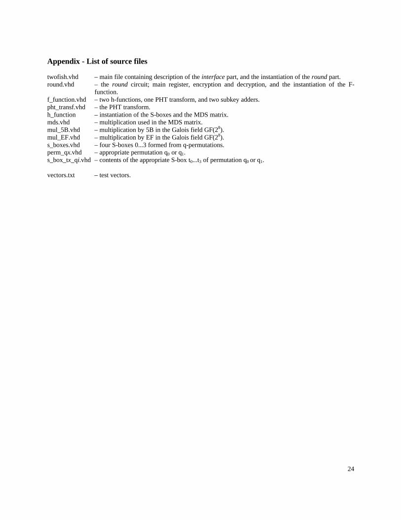
Appendix - List of source files
twofish.vhd – main file containing description of the interface part, and the instantiation of the round part.round.vhd – the round circuit; main register, encryption and decryption, and the instantiation of the F-
function.f_function.vhd – two h-functions, one PHT transform, and two subkey adders.pht_transf.vhd – the PHT transform.h_function – instantiation of the S-boxes and the MDS matrix.mds.vhd – multiplication used in the MDS matrix.mul_5B.vhd – multiplication by 5B in the Galois field GF(28).mul_EF.vhd – multiplication by EF in the Galois field GF(28).s_boxes.vhd – four S-boxes 0...3 formed from q-permutations.perm_qx.vhd – appropriate permutation q0 or q1.s_box_tx_qi.vhd – contents of the appropriate S-box t0...t3 of permutation q0 or q1.
vectors.txt – test vectors.