impact of magnetic micro-seeds in electronic package solder joint suitability projects... ·...
TRANSCRIPT

Impact of Magnetic Micro-Seeds in Electronic
Package Solder Joint Suitability
Period of Activity
AY 2015/2016 Semester 1 and 2
By: Supervisors:
Yau Ding Hua Tricia Dr. Gopala Krishnan
Ramaswami
A0102362X A/P Tok Eng Soon
In partial fulfilment of PC4199 Honours Project in Physics
Faculty of Science, Physics Department

i
Acknowledgement
I would like to sincerely acknowledge various people who have been with me in this
academic year where I have worked on my thesis. Firstly, a great part of this journey would
not be possible without my supervisors – Dr. Gopala Krishnan Ramaswami and A/P Tok Eng
Soon. Their valuable input and continuous guidance have helped me a great extend to the
completion of this work. I would also like to thank Mr. Arun Kumar Seraaj for his extensive
help thoughout this journey. He has been a great mentor and would always ensure that I do
not make any major mistakes in my work. I would also like to thank Dr. Ong Sheau Wei and
Mr. Chen Chang Pang, whom also belongs in εMaGIC Laboratory, they have helped me in
experimental procedures and discussions. I take this opportunity to also appreciate various
people in NUS Physics Department – Mr Chen Gin Seng, Mr Ho Kok Wen, Mrs Lee Soo
Mien and Mrs. Ng Soo Ngo for their support in equipment and technicalities. Lastly, I wish
to express my sense of gratitude to my family and friends who have been, directly or
indirectly, lending their helping hands and giving me encouragement to get me through the
project.
ii
Abstract
SAC305 is regarded as the top-performing environmentally friendly solder to date. However,
there are challenges to this solder such as its higher melting temperature which may cause
excessive intermetallic growth at solder/substrate interfaces. Adding ferromagnetic materials
into SAC305 has the potential to alleviate the challenges faced as it gives rise to an
alternative to the conventional global reflow process – magnetic induction heating. This
localised heating method prevents the temperature of other parts of the electronic package to
be highly elevated.
The first phase of this work involves the characterization of the as-made material. Fe is
incorporated into SAC305 through the process of ball-milling. The Fe-SAC305 composite
materials were characterized using Scanning Electron Microscopy and Energy-dispersive X-
ray Spectroscopy (SEM-EDX), Vibrating Sample Magnetometer (VSM) and Differential
Scanning Calorimetry (DSC). SEM-EDX was used to analyse the chemical composition of
the as-made solder materials and also to study the microstructure of Fe particles. VSM was
used to characterise its magnetic properties. It has been found that the usefulness of the
magnetic properties of Fe has not been changed after the process of ball-milling. DSC was
used to analyse its thermal properties. The change in melting temperature is less than 1°C
when Fe content increases to 25wt%. This change in melting temperature is insignificant in
the industrial process since it still falls within the solder melting temperature range.
The second phase of this work is a preliminary experimentation on the solder joint. The flake
samples were placed on an industrial Cu Ball Grid Array substrate. From the small sampling,
it seems that wettability is not promoted with the addition of Fe. Due to time constraint,
SEM-EDX was not done to identify the Fe particles at the cross-sections of the solder joint.
This is important as Fe has a higher density than SAC305 and is predicted to sink to the
solder joint interface. This may be detrimental to the strength of the solder joint as well as the
conductivity. However, caution needs to be taken while evaluating the preliminary data. With
the VSM and DSC results, the theoretical magnetic induction heating time is calculated. With

iii
an alternating magnetic field frequency of 280kHz, the induction heating times are able to
reach less than 10s for Fe content of 15wt% and above.
In conclusion, this work shows the potential of ball-milled Fe-SAC305 system solders to be
of great impact to the electronic packaging industry. More studies need to be conducted to
obtain the optimal characteristics of Fe-SAC305 system solder suited to harness Fe as heat-
generating magnetic micro-seeds in magnetic induction heating.

iv
Table of Contents
Acknowledgement ..................................................................................................................... i
Abstract ..................................................................................................................................... ii
Table of Contents .................................................................................................................... iv
List of Figures .......................................................................................................................... vi
List of Tables ............................................................................................................................ x
Chapter 1 Introduction ...................................................................................................... 1
1.1 Microelectronic Packaging ............................................................................................ 1
1.2 Solder and Solder Joint .................................................................................................. 2
1.3 Lead-free Solder Material Journey ................................................................................ 5
1.4 Fe-SAC305 System ........................................................................................................ 8
1.5 Research Objectives and Scope of Thesis ................................................................... 14
Chapter 2 Methodology ................................................................................................... 15
2.1 Overview ...................................................................................................................... 15
2.2 Sample Preparation for Fe-SAC305 Solder ................................................................. 15
2.3 Sample Preparation for solder/substrate Fe-SAC305/Cu joint .................................... 17
2.4 Characterization Techniques ........................................................................................ 21
2.4.1 Scanning Electron Microscopy and Energy-dispersive X-ray Spectroscopy
(SEM-EDX) ...................................................................................................................... 21
2.4.1 Vibrating Sample Magnetometer (VSM)......................................................... 24
2.4.1 Differential Scanning Calorimetry (DSC) ....................................................... 26
Chapter 3 Impact of Fe on SAC305................................................................................ 28
3.1 Solder Composition, and Fe Content and Distribution: SEM-EDX ............................ 28
3.2 Magnetic Properties: VSM .......................................................................................... 33
3.3 Thermal Properties: DSC ............................................................................................. 37
Chapter 4 Fe-SAC Solder Applicability to industrial Cu BGA ................................... 44
4.1 Impact of Fe on Cross-section of Solder/Substrate ...................................................... 44
4.2 Magnetic Induction Heating Applicability .................................................................. 49
Chapter 5 Conclusion and Future Work ....................................................................... 53

v
5.1 Conclusion ................................................................................................................... 53
5.2 Future Work ................................................................................................................. 54
References ............................................................................................................................... 56
Chapter 6 Appendices ...................................................................................................... 62
6.1 Appendix I: Phase Diagram and Gibbs Free Energy of Fe-Sn system ........................ 62
6.2 Appendix II: SEM-EDX .............................................................................................. 63
6.3 Appendix III: Calculated Expected Values of Saturation Magnetization for Fe-
SAC305 System .......................................................................................................... 83
6.4 Appendix IV: Miscellaneous DSC Experimental Results ........................................... 83
6.5 Appendix V: Solder Joint Features .............................................................................. 86
6.6 Appendix VI: IMC Measurement Methodology.......................................................... 89
6.7 Appendix VII: Calculated Values of Induction Heating Time .................................... 90

vi
List of Figures
Figure 1. 1 Multi-level packaging in microelectronics [2]. .................................................................... 1
Figure 1. 2 (a) Schematic of Flip Chip Solder Joint Technology. (b) Optical Micrograph of BGA with
7x6 Cu pads............................................................................................................................................. 2
Figure 1. 3 (a) Optical micrograph of cross-section of SAC305 solder ball on Cu pad. (b) zoom-in of
interfacial region of (a). .......................................................................................................................... 3
Figure 1. 4 Temperature profile for reflow soldering process for SAC305 and Sn96.5/Ag3.5 solders
[12] .......................................................................................................................................................... 4
Figure 1. 5 Reflow window for Sn-Pb and Pb-free solders [5] ............................................................... 6
Figure 1. 6 SEM micrograph of SAC305 [11] (b) and (c) SAC305 solder joint failure in thermal
cycling [14] ............................................................................................................................................. 7
Figure 1. 7 Schematic diagram of reflow process using magnetic induction heating ............................. 8
Figure 1. 8 magnetic induction heating responses of studied alloys with (a) dispersions of different
magnetic elements. (c) Fe dispersions at different concentrations. [25] ............................................... 10
Figure 1. 9 Plot of conductivities and densities of Fe, FeSn, FeSn2, SAC305 and Sn .......................... 12
Figure 1. 10 (a) FeSn2 phase in solder bulk [33] (b) Fe particles near interfacial region; (c) pure Fe
particles surrounded by FeSn2 ............................................................................................................... 13
Figure 2. 1 RETSCH Planetary Ball Mill PM400 ................................................................................ 16
Figure 2. 2 (a) Optical Microscope BX51; (b) Application of flux and solder under optical
microscope; (c) samples placed in porcelain boat................................................................................. 18
Figure 2. 3 Furnace reflow experimental set-up ................................................................................... 19
Figure 2. 4 (a) Preparation of sample for polishing; (b) Struers Tegramin-20 Polishing Machine ...... 20
Figure 2. 5 (a) Electrons and photon signals emanating from volume during electron-beam
impingement. (b) energy spectrum of electrons emitted. (c) effect of surface topography on electro
emission. [44] ........................................................................................................................................ 22
Figure 2. 6 Schematic diagram of x-ray emission................................................................................. 22
Figure 2. 7 JEOL Field Emission Scanning Electron Microscope JSM-6700F .................................... 23
Figure 2. 8 Typical Magnetic hysteresis loop of a ferromagnetic material [46] ................................... 25
Figure 2. 9 Pellet sample ....................................................................................................................... 25
Figure 2. 10 Typical DSC profile for BM SAC305 .............................................................................. 26

vii
Figure 3. 1 SEM micrograph, EDX map spectrum and corresponding EDX elemental maps of Sn, Fe,
C, Cu, Ag and O for 25wt%Fe-SAC. .................................................................................................... 29
Figure 3. 2 At% of elements in all 3 images (I1, I2 and I3) obtained from map spectrum data. Images
can be found in Appendix. .................................................................................................................... 30
Figure 3. 3 Fe/Sn atomic ratio as a function of theoretical Fe wt% ...................................................... 31
Figure 3. 4 All Fe EDX chemical maps from 5wt% to 25wt%. ............................................................ 32
Figure 3. 5 Fe-rich area marked with red marks for (a) 5wt%Fe-SAC and (b) 25wt%Fe-SAC. .......... 32
Figure 3. 6 Hysteresis curves for BM SAC305 and 6 compositions of Fe-SAC system in wide scan
range of -15000Oe to +15000Oe. ......................................................................................................... 34
Figure 3. 7 Graphs of experimental and expected Saturation Magnetization as a function of mass of Fe
present in sample. .................................................................................................................................. 35
Figure 3. 8 Hysteresis curves for BM SAC305 and 6 compositions of Fe-SAC system in narrow scan
range of -100Oe to +100Oe. ................................................................................................................. 36
Figure 3. 9 Hysteresis loss of BM SAC305 and Fe-SAC305 system. .................................................. 36
Figure 3. 10 DSC Curves for ball-milled samples with Fe wt% from 0wt% to 25wt%. Curves are
vertically displaced by -15 mW progressively. ..................................................................................... 38
Figure 3. 11 Data plots of Latent Heat of Fusion against Mass of Sn for all heats of BM SAC305 with
y ≡ Latent Heat of Fusion in mJ and x ≡ Mass of Sn in mg .............................................................. 39
Figure 3. 12 Latent Heat of Fusion against Mass of Sn in sample ........................................................ 40
Figure 3. 13 Minimum and experimental moles of Sn against moles of Fe in sample ......................... 42
Figure 3. 14 DSC curves for 1st, 2nd and 3rd heating for (a) BM SAC (b) 2wt%Fe-SAC (c) 5wt%Fe-
SAC (d) 10wt%Fe-SAC (e) 15wt%Fe-SAC (f) 20wt%Fe-SAC (g) 25wt%Fe-SAC ............................ 43
Figure 4. 1 Optical micrographs of as-received Cu pads with (a) 50x and (b) 100x objective lens
magnifications. ...................................................................................................................................... 46
Figure 4. 2 Cross-section of 7 Cu pads on BGA for (a) B SAC305 and (b) 25wt%Fe-SAC ............... 47
Figure 4. 3 100x objective lens on cross-sections of (a) BM SAC305 and (b) 25wt%Fe-SAC solder
joints ...................................................................................................................................................... 47
Figure 4. 4 Induction heating time as a function of frequency of alternating magnetic field for BM
SAC305 and Fe-SAC system. ............................................................................................................... 51
Figure 6. 1 Fe-Sn phase diagram .......................................................................................................... 62
Figure 6. 2 Graph of Gibbs Free Energy of FeSn and FeSn2 in temperature range of 25°C to 325°C 63
Figure 6. 3 SEM micrographs for 5wt%Fe-SAC flakes. (a), (b) and (c) are 100x100µm sizes while
(d), (e) and (f) are the corresponding 10x10µm images marked by the red boxes. .............................. 64

viii
Figure 6. 4 SEM micrographs for 25wt%Fe-SAC flakes. (a), (b) and (c) are 100x100µm sizes while
(d), (e) and (f) are the corresponding 10x10µm images marked by the red boxes. .............................. 64
SEM image for BM SAC305
Figure 6. 5 250x250µm I1 .................................................................................................................... 65
Figure 6. 6 250x250µm I2 .................................................................................................................... 65
Figure 6. 7 250x250µm I3 .................................................................................................................... 66
Figure 6. 8 100x100µm I1 .................................................................................................................... 66
Figure 6. 9 100x100µm I2 .................................................................................................................... 67
Figure 6. 10 100x100µm I3 .................................................................................................................. 67
SEM image for 5wt%Fe-SAC
Figure 6. 11 250x250µm I1 .................................................................................................................. 68
Figure 6. 12 250x250µm I2 .................................................................................................................. 68
Figure 6. 13 250x250µm I3 .................................................................................................................. 69
Figure 6. 14 100x100µm I1 .................................................................................................................. 69
Figure 6. 15100x100µm I2 ................................................................................................................... 70
Figure 6. 16 100x100µm I3 .................................................................................................................. 70
SEM image for 10wt%Fe-SAC
Figure 6. 17 250x250µm I1 .................................................................................................................. 71
Figure 6. 18 250x250µm I2 .................................................................................................................. 71
Figure 6. 19 250x250µm I3 .................................................................................................................. 72
Figure 6. 20 100x100µm I1 .................................................................................................................. 72
Figure 6. 21 100x100µm I2 .................................................................................................................. 73
Figure 6. 22 100x100µm I3 .................................................................................................................. 73
SEM image for 15wt%Fe-SAC
Figure 6. 23 250x250µm I1 .................................................................................................................. 74
Figure 6. 24 250x250µm I2 .................................................................................................................. 74
Figure 6. 25 250x250µm I3 .................................................................................................................. 75
Figure 6. 26 100x100µm I1 .................................................................................................................. 75
Figure 6. 27 100x100µm I2 .................................................................................................................. 76
Figure 6. 28 100x100µm I3 .................................................................................................................. 76
SEM image for 20wt%Fe-SAC
Figure 6. 29 250x250µm I1 .................................................................................................................. 77
Figure 6. 30 250x250µm I2 .................................................................................................................. 77
Figure 6. 31 250x250µm I3 .................................................................................................................. 78
Figure 6. 32 100x100µm I1 .................................................................................................................. 78
Figure 6. 33 100x100µm I2 .................................................................................................................. 79
Figure 6. 34 100x100µm I3 .................................................................................................................. 79

ix
SEM image for 25wt%Fe-SAC
Figure 6. 35 250x250µm I1 .................................................................................................................. 80
Figure 6. 36 250x250µm I2 .................................................................................................................. 80
Figure 6. 37 250x250µm I3 .................................................................................................................. 81
Figure 6. 38 100x100µm I1 .................................................................................................................. 81
Figure 6. 39 100x100µm I2 .................................................................................................................. 82
Figure 6. 40 100x100µm I3 .................................................................................................................. 82
Figure 6. 41 DSC curves of Stearic Acid 1st, 2nd and 3rd heating. ..................................................... 83
Figure 6. 42 (a), (c) and (e) DSC curves of 1st, 2nd and 3rd heating respectively for 5 different sample
masses. (b), (d) and (f) plots of Latent Heat of Fusion against Mass of Sn for 1st, 2nd and 3rd heating
respectively. Curves are vertically displaced by -15 mW p .................................................................. 85
Figure 6. 43 Cu pads peeling at area without solder joints ................................................................... 86
Figure 6. 44 Black spots in interfacial regions and solder bulk ............................................................ 87
Figure 6. 45 Close up of 7 Cu pads for BM-SAC305 ........................................................................... 87
Figure 6. 46 Close up of 7 Cu pads for 25wt%Fe-SAC ........................................................................ 88
Figure 6. 47 Some solder bulks which appear detached from Cu pads. Thin red arrows show solder
bulks with no IMCs observed. Thick dotted blue arrows show solder bulks with IMCs observed. ..... 88
Figure 6. 48 Rectangular features which may be Ag3Sn platelets ....................................................... 89
Figure 6. 49 IMC thickness measurement methodology (a) average height and (b) area/length
methodologies ....................................................................................................................................... 89
Figure 6. 50 Both methodologies used to measure IMC thickness with x length of 30µm, 70µm and
100µm. .................................................................................................................................................. 90

x
List of Tables
Table 1. 1 Different stages of reflow process and their purposes. .......................................................... 4
Table 1. 2 Family of lead-free solder compounds and their respective melting temperature and relative
price [10] ................................................................................................................................................. 5
Table 1. 3 Addition of reinforcements to SAC305 [6]............................................................................ 7
Table 1. 4 Summary of impact on solder after Fe addition ................................................................... 11
Table 2. 1 Compositions of Fe-SAC305 samples made in mass and atomic weight percentages ........ 17
Table 2. 2 Typical industrial and furnace reflow profiles ..................................................................... 19
Table 2. 3 Polishing parameters ............................................................................................................ 20
Table 2. 4 Values of Characteristic X-Ray Energies [45] ..................................................................... 23
Table 2. 5 Values of weight and atomic percentages of Fe and Sn for different compositions of Fe-
SAC305 ................................................................................................................................................. 24
Table 2. 6 (a) Masses of pellet samples used; (b) VSM applied magnetic field range ......................... 25
Table 2. 7 Experimental and reference values for onset temperature and specific latent heat of fusion
for Indium ............................................................................................................................................. 27
Table 2. 8 Various masses of (a) SAC305 and BM SAC305, (b) different compositions of Fe-
SAC305. ................................................................................................................................................ 27
Table 3. 1 At% of Fe, Sn and Stearic Acid (S.A.) present in different compositions of Fe-SAC system.
.............................................................................................................................................................. 30
Table 3. 2 Values of Retentivity, Coercivity and Saturation Magnetization of Fe, BM Fe, SAC305 and
BM SAC305 for wide scan range of -15000Oe to +15000Oe. ............................................................. 33
Table 3. 3 Values of Retentivity, Coercivity and Saturation Magnetization of BM SAC305 and 6
compositions of Fe-SAC system. .......................................................................................................... 34
Table 3. 4 Average onset and peak melting temperatures of SAC305 and BM SAC305. .................... 38
Table 3. 5 Onset and peak melting temperatures for 1st heating. ......................................................... 39
Table 3. 6 Values of calculations leading to masses and moles of Sn reacted. ..................................... 41
Table 3. 7 Values of calculations leading to minimum masses and moles of Sn if all Fe has reacted. 41
Table 4. 1 Values of heat capacities used ............................................................................................. 49
Table 4. 2 Values required for induction heating time calculation. ...................................................... 50

xi
Table 4. 3 Heating power with alternating magnetic field frequency of 280kHz. ................................ 51
Table 6. 1 SEM-EDX experimental parameters for preliminary experimentation ............................... 63
Table 6. 2 Methodology Parameters used for SEM-EDX Experimentation ......................................... 64
Table 6. 3Experimental and expected values of saturation magnetization from VSM result ............... 83
Table 6. 4 Temperatures for various masses of SAC305 ...................................................................... 84
Table 6. 5 Temperatures for various masses of BM SAC305 ............................................................... 84
Table 6. 6 Temperatures for Fe-SAC305 system .................................................................................. 84
Table 6. 7 BM SAC305 for 1st, 2nd and 3rd heats ............................................................................... 86
Table 6. 8 Fe-SAC305 system for 1st, 2nd and 3rd heats ..................................................................... 86
Table 6. 9 Results from both methodology ........................................................................................... 90
Table 6. 10 Induction heating time between frequency range of 10kHz to 600kHz ............................. 90
1
Chapter 1
Introduction
1.1 Microelectronic Packaging
With the requirements of advanced electronic products (GoPro, iWatch, Fitbit and the like) to
be faster, lighter and smaller, the interconnections between a Si chip and a bonding pad are
driven to be denser than ever. Generally, there are three levels of interconnections in
microelectronic packaging. The first-level refers to connections between pins of the package
substrate and bonding pads on the integrated circuit [1]. The second-level involves discrete
devices on printed circuit boards and the third-level deals with the accessibility by arranging
subsystems together [2].
Figure 1. 1 Multi-level packaging in microelectronics [2].
For high-density Input/Output (I/O) pads, flip chip solder joint technology has been widely
harnessed in the first- and second-level packaging. As in Fig. 1.2 (a), the Si chip is flipped
facing down on a substrate with the electrical connections achieved through an area array of
solder bumps [3]. An optical micrograph of a ball grid array (BGA) is shown in Fig. 1.2(b).
The advantage of this methodology over conventional wire-bonding is that the solder bumps
cover a large part of the chip surface rather than merely the periphery in wire-bonding.

2
Figure 1. 2 (a) Schematic of Flip Chip Solder Joint Technology. (b) Optical Micrograph of
BGA with 7x6 Cu pads
1.2 Solder and solder joint
A solder is the interconnect material for integrated consumer electronic system. In addition to
being an electrical conduit, it acts as a thermal path and mechanically holds the parts together
[4]. A solder joint is essentially the chemical reaction between Sn (in solder) and Cu
(substrate) to form intermetallic compounds (IMCs). Therefore, Cu-Sn is arguably one of the
most important metallurgical binary system that has impacted human civilization [3].
A good solder should henceforth have the following key properties [5,6,7]:
I. Eutectic composition. Its melting point has to be lower than its individual components
and it behaves like a pure solid with a single melting temperature. This ensures that
both interfaces can join at the same time.
II. Low melting temperature. This is to avoid damage to other parts of the electronic
package.

3
III. Good wetting ability. This refers to the capability of an alloy in molten state to spread
over a metal surface. For good wetting, the contact angle, related surface tensions of
substrate/flux and substrate/solder interfaces, needs to be small.
IV. Good mechanical properties, such as hardness and modulus, tensile properties,
thermomechanical fatigue and the likes. It gauges the reliability of consumer products
when subjected to stress in operation environment.
V. Good thermal properties, such as reasonable thermal conductivity and low coefficient
of thermal expansion. Similarly, it gauges how reliable the product operation is.
VI. Good electrical properties. Since solder serves as an electrical interconnect, its
electrical resistivity should be low to allow current flow. Further, due to the trend
towards high I/O density, electro-migration becomes an increasingly worrying issue.
High current density causes atoms to migrate in the general direction as electron flow
which may produce voids. There may also be directional effects on IMC growth
resulting in reliability issues.
VII. Low cost. Microelectronics industry is extremely cost-conscious to continuously
produce higher performance at lower costs.
VIII. Environmentally-friendly. This is due to legislation that eliminates the use of Pb due
to environmental and toxicological concerns.
The physical properties a good solder joint should have are mainly attributed to the
characteristics of the interfacial IMCs as it may adversely affect the reliability and
solderability of solder joints should excessive growth occurs during storage and service [8].
Fig. 1.3 shows an optical micrograph of interfacial IMCs. The IMCs present in the solder
bulk might have been detached from the interfacial IMCs. The characteristics of IMCs are
further discussed in section 1.3.
Figure 1. 3 (a) Optical micrograph of cross-section of SAC305 solder ball on Cu pad. (b)
zoom-in of interfacial region of (a).

4
To form a solder joint, reflow solder is performed. It is the process in which solder paste is
used to attach electrical components to their contact pads i.e. Si chip to Cu pad. The entire
assembly would be subjected to controlled heat so as to melt and permanently connect the
components together [5]. This means that global heating is involved. Fig. 1.4 shows a typical
reflow temperature profile. The profile is developed with the goal of attaining a reliable and
repeatable reflow process which optimises wetting properties and minimises peak reflow
temperature at the same time. It consists of 4 stages – pre-heating, soaking, reflow and
cooling. The purpose of each stage is summarised in Table 1.1.
Table 1. 1 Different stages of reflow process and their purposes.
Figure 1. 4 Temperature profile for reflow soldering process for SAC305 and Sn96.5/Ag3.5
solders [12]

5
1.3 Lead-free solder material journey
The conventional primary solder used, 63Sn-37Pb, is considered to be environmentally
hazardous due to Pb toxicity [7]. According to the Directive on Waste from Electrical and
Electronic Equipment, the use of Pb is to be phased out from January 2004 onwards [7,9].
Since then, the global electronic assembly community has been striving to search for the best
replacement. Table 1.2 shows an example of 5 prominent solders named after their
metallurgical compositions.
Table 1. 2 Family of lead-free solder compounds and their respective melting temperature
and relative price [10]
SAC305 (Sn-3wt%Ag-0.5wt%Cu), in particular, is currently the most favourable
environmentally-friendly solder used. This is due to its low melting temperature of about
217°C, its near-eutectic composition and favourable thermal-mechanical fatigue properties
[11]. This high-performing solder material therefore has many stakeholders such as Indium
Corporation and Infineon which produces the material itself; Global Foundries and ST
Microelectronics which uses the material in their chips; and finally, Samsung and Apple
which uses these chips in the making of consumer products.
However, since it differs from Sn-Pb solders in soldering performance, microstructures and
mechanical behaviours, it creates key challenges which must be addressed in order for it to be
successfully implemented into consumer electronics applications [4]. There are two main
issues at hand – high reflow temperature and reliability issues due to microstructural
phenomena.

6
High Reflow Temperature
As mentioned in section 1.2, packages need to reach a temperature of at least 20°C higher
than the solder melting temperature to form a good solder joint. Fig. 1.5 shows the higher
reflow temperature required as compared to Sn-Pb solders. The peak reflow temperatures are
projected to rise to about 240°C to 260°C while temperature-sensitive electronic components
can tolerate a maximum temperature of about 240°C [13]. Further, due to the inferior wetting
characteristics of SAC305, the reflow soldering window is slightly longer (40-120 seconds)
[5]. These bring about increased damages such as PCB warpages, interfacial delamination
and electrical failure if interconnect lines are broken [4].
Figure 1. 5 Reflow window for Sn-Pb and Pb-free solders [5]
Microstructural Phenomena
The micro-constituents in SAC305 solder are typically large plates of primary Ag3Sn, large
needles of Cu6Sn5 and dendritic β-Sn. Their presence is attributed to the large undercooling
of Sn which starts to nucleate homogeneously after being undercooled for a period of time.
The delay causes the microstructural development of solidified Sn-based alloys which thus
affects the mechanical properties of solder joints adversely [5]. Further, IMCs at
solder/substrate interface also degrade mechanical properties as they can become sites for
crack initiation and propagation if it becomes a significant fraction of the solder joint [4].

7
Figure 1. 6 SEM micrograph of SAC305 [11] (b) and (c) SAC305 solder joint failure in
thermal cycling [14]
With the demands of electronic manufacturing industry based on cost, reliability and shelf
life [10], reinforcements have been added to address the challenges as shown in Table 1.3.
The impact of reinforcements aims for key properties of a good solder mentioned in section
1.2.
Table 1. 3 Addition of reinforcements to SAC305 [6]
Of particular interest would be the addition of ferromagnetic elements (Fe, Ni or Co). Its
magnetic property has the prospective to improve the two main issues of high reflow
temperature and microstructural phenomena which is elaborated in section 1.4.

8
1.4 Fe-SAC305 system
Magnetic Induction Heating
Incorporating ferromagnetic material into solders make them suitable for heating via
magnetic induction – a localised heating methodology (as opposed to global heating in
conventional reflow process). Shown in Fig. 1.7, the assembly would be placed at the centre
of an induction coil. With a high frequency electromagnetic field, ferromagnetic particles
which are homogeneously distributed within the solders are able to dissipate energy via eddy
currents, hysteretic and relaxation processes. This means that they can be harnessed as
localised heat-generating micro-seeds to uniformly heat up and melt the solders.
Additionally, the control of the application of magnetic field can act as a manipulative tool
not only for the control of solder melting during fabrication; but also for other functionalities
such as microelectronic repairs and the like.
Figure 1. 7 Schematic diagram of reflow process using magnetic induction heating
Eddy Currents
Eddy currents are generated in accordance to Lenz’s law - these currents would subsequently
induce an electric field to oppose the change in magnetic flux of the applied field. This results
in Joule heating within the conductors with eddy currents power loss in a material as follows
from Stephensons’ equation:

9
Pec =π2
β
B2f2
ρd2 Wm
-3 with 𝐵 = 𝜇0(𝐻 + 𝑀)
(1.1) [5,21]
where 𝛽 ≡ shape-factor coefficient (equals to 20 for spheres), 𝜇0 ≡ vacuum permeability, H ≡
applied field strength, M ≡ material magnetization, f ≡ frequency of applied field , 𝜌 ≡ bulk
resistivity of the materials and d ≡ cross-sectional dimension (equivalent to diameter for
spheres).
It should be noted that eddy current power loss is negligible for solder powders with diameter
of 50µm or less and do not contribute significantly to heating [21,22].
Hysteresis
Hysteresis is at the heart of the behaviour of magnetic materials [23]. In 1907, Weiss
proposed that a ferromagnetic material is subdivided into regions called magnetic domains.
The magnetization orientation can vary from domain to domain but it is aligned within the
domain [23]. The material gets magnetized when its domains align to an applied field. This
magnetization retains after the applied field is removed unless effort is made to demagnetise
it. Hence, a closed path magnetization curve can be plotted with a varying applied field. This
is known as a hysteresis loop - a detailed discussion is in section 2.4.2.
Relaxation
Magnetic nanoparticles become superparamagnetic below a certain critical size [22].
Relaxation processes then take place due to the thermal relaxation of magnetic moments in
the material [5]. The characteristics of a hysteresis loop do not apply if the measurement time
is larger than the relaxation time of the system which results in relaxation being the dominant
mechanism of power loss [5, 22, 24].
Background
In this project, the ferromagnetic material of choice would be Fe as it is most useful for
magnetic induction heating application. According to Calabro et al. [25], SnAg alloys
containing Fe dispersions are able to inductively heat up at a faster rate than Ni or Co
10
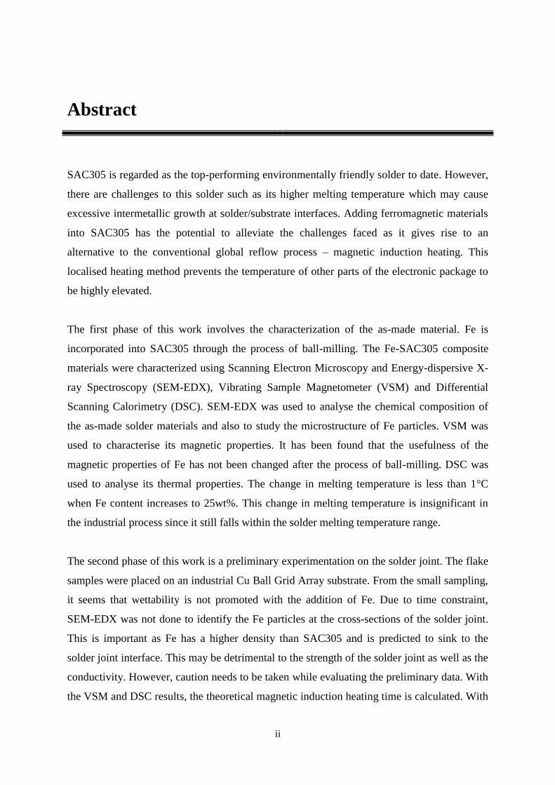
dispersions (Fig. 1.8(a)). It is also noted that higher concentration of Fe produced faster
heating as expected (Fig. 1.8(b)).
Figure 1. 8 magnetic induction heating responses of studied alloys with (a) dispersions of
different magnetic elements. (c) Fe dispersions at different concentrations. [25]
Various studies on Fe reinforcements have been done for Sn-Ag-Cu solders as shown in
Table 1.4.

11
Table 1. 4 Summary of impact on solder after Fe addition
12
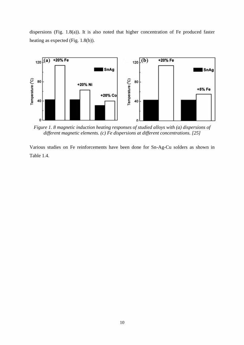
With reference to the phase diagram as shown in Appendix, the possible phase formation at
typical reflow temperature would be FeSn2 and FeSn. Therefore, the expected additions to a
solder joint interface would be Fe, FeSn and FeSn2. Fig. 1.9 shows the relative densities and
resistivities of Fe, FeSn, FeSn2, SAC305 and Sn. Since the densities of Fe-Sn phases are
higher than SAC305, when Fe-SAC305 system solder is melted onto a substrate, Fe-Sn
phases are expected to sink to the interface during cooling. The wettability is expected to
decrease since Fe-Sn phases would take up the spaces for IMC growth which is required for a
good solder joint. The conductivity of FeSn and FeSn2 are much lower. Hence, the interfacial
contact conductivity may decrease with their formation. Since the IMCs are denser than their
end members (Fe and Sn), they act as scattering sites for conduction of electrons. A higher
density causes electrons to be scattered more. This in turn causes electrical conductivity to
decrease [34].
Figure 1. 9 Plot of conductivities and densities of Fe, FeSn, FeSn2, SAC305 and Sn
[31, 34-37]
FeSn2 have been observed in solder bulk and interfacial region in previous studies as
mentioned in Table 1.4. Fig. 1.10(a) shows the presence of FeSn2 sparsely distributed in
solder bulk of Fe-SAC105 [33]; Fig. 10(b) and (c) show the presence of Fe-rich regions at
interfacial area in Fe-SAC305. FeSn2 phase forms around pure Fe particles, and the thickness
of FeSn2 increased from hundreds of nanometers to 1µm from reflow time of one minute
onwards [31].

13
Figure 1. 10 (a) FeSn2 phase in solder bulk [33] (b) Fe particles near interfacial region; (c)
pure Fe particles surrounded by FeSn2
The addition of Fe allows localised reflow to occur, which may mitigate some of the current
challenges of SAC305 solders. However, their addition causes concern such as the reduction
in the strength of solder joints and also decrease in conductivity. Both of which are
detrimental to the electronic packaging reliability. Therefore, the impact of Fe in SAC305 as
a solder material and as a solder joint on a substrate is crucial information in the
determination of the capability of Fe-SAC305 system solder.
1.5 Research Objectives and Scope of Thesis
The scope of the thesis would be to investigate the suitability of Fe-SAC305 as a solder
material and as a solder joint on Cu BGA. The modification in properties after Fe-SAC305 is
subjected to thermal impact is studied. There are 3 main objectives in this project.
I. Impact of Fe on SAC305 through magnetic and thermal properties of Fe-SAC305
system.
II. Study of Fe as magnetic micro-seeds by evaluating Fe distribution within SAC305.
III. Assess the impact of Fe-SAC305 system on Cu interface
The first phase involves characterization of Fe-SAC305 system. The magnetic and thermal
properties are studied using Vibrating Sample Magnetometer (VSM) and Differential
Scanning Calorimetry (DSC) respectively (objective 1). The spatial distribution is studied
using Scanning Electron Microscopy and Energy-dispersive X-ray Spectroscopy (SEM-EDX)
(objective 2). The second phase occurs after forming a solder joint with Fe-SAC305 and Cu

14
BGA. The interfacial impact is studied using SEM-EDX and Optical Microscopy (OM)
coherently (objective 3).

15
Chapter 2
Methodology
2.1 Overview
This chapter introduces the sample preparation – how Fe was incorporated into SAC305 by
ball-milling. It describes the methodology used to prepare a solder joint between Fe-SAC
system and a Cu pad by furnace reflow. The characterization techniques used in this project –
SEM-EDX, VSM and DSC are also presented in terms of the working principles, instruments
and parameters involved.
2.2 Sample Preparation for Fe-SAC305 solder
The samples were prepared by a process called ball-milling. Ball-powder-ball collisions
causes powder particles to repeatedly flatten, cold-weld, fracture and re-weld [38]. This is
because a small amount of particles will be trapped between the grinding balls during impact.
Soft metal particles will plastically deform and cold-weld while brittle metal particles (e.g.
Fe) tend to fracture. Work hardening may also occur to the soft metals which results in their
fracture thereafter. Subsequently, the freshly fractured particles may then again cold-weld.
The continual ball-ball, ball-powder and ball-wall collisions will cause a rise in temperature,
which promotes diffusion and thus microstructural refinement. Eventually, the competing
events of cold-welding and fracturing result in a homogenized microstructure. The final result
should be a compositions of individual powders equivalent to the composition of the starting
material. This is known as the steady state equilibrium where there is a balance between the
rate of welding and fracturing. The former tends to increase while the latter decreases particle
size. If the aim is to decrease particle size, the particle surfaces can be modified by adding a
processing control agent (PCA) which impedes fresh surface contact necessary for cold
welding. This is because PCA are surface-active agents which are absorbed on the surfaces to
inhibit agglomeration [38]. Since PCAs such as stearic acid consists of carbon, hydrogen and

16
oxygen, they may become incorporated in the powder particles in the form of inclusions or
dispersoids and also result in the formation of carbides and oxides [38].
Besides obtaining a homogenized microstructure, the reduction of particle size can lead to a
decrease in melting point. This is due to excess energy stored in the grain boundaries as well
as the capillarity which causes a reduction in total enthalpy of melting [39]. Melting point
depression is as abovementioned in Section 1.2 an interest in microelectronic packaging.
Another advantage of milling is the possibility of the retardation of interfacial IMCs
formation [40].
Equipment Parameters and Sample Preparation
In making a homogeneous mixture of Fe and SAC305, Fe powder (Alfa Aesar,
LOT:10174355, 99% purity) was introduced into SAC305 (Qualitek, LOT:305Y13M06T3),
with addition of 3wt% PCA Stearic acid (Alfa Aesar, LOT: 10148625,98% purity) by
mechanical ball-milling. Stearic acid was added to prevent cold-welding of the powder. The
equipment used as shown in Fig. 2.1 was RETSCH Planetary Ball Mill PM400, with stainless
steel milling jars (diameter: 45.0mm; capacity: 50ml; depth: 30.0mm) and ball bearings
(mass: 0.5g/ball; diameter: 5.0mm).
Figure 2. 1 RETSCH Planetary Ball Mill PM400

17
A total of 10g of materials (Fe + SAC305) and 0.3g of Stearic Acid was used in each jar. The
compositions (mass and at%) of the samples made are as shown in Table 2.1. This table gives
the name adopted throughout the thesis and composition of Fe-SAC system used for
subsequent characterization and experimentation. The total milling time was 25 hours, with a
milling-rest interval of 30 minutes and rotation rate of 250 rpm.
Table 2. 1 Compositions of Fe-SAC305 samples made in mass and atomic weight
percentages
2.3 Sample Preparation for solder/substrate Fe-SAC/Cu joint
preparation
Choice of Cu Substrate
The choice of Cu substrate was the industrial Cu BGA as shown in Fig. 2.2(b). This is
because the formation of solder joint with Cu BGA has direct industrial application. The Cu
on BGA differs from usual Cu due to an additional layer of Organic Solderability
Preservative (OSP) on it. OSP contains the activated compound arylphenylimidazole (API)
such as benzimidazole. This additional layer, typically 0.2µm to 0.3µm [41], resists oxygen
penetration thereby minimizing Cu oxidation; prevents degradation of solderability [42] and
also acts as an adhesion promoter [43]. Therefore, as compared to a solder joint with a Cu
foil, the reaction rate is not as quick. This means that the IMC thickness would be smaller.
Sample SAC305 Fe S.A. SAC305 Fe Sn S.A.
BM SAC305 10.0 0.0 0.3 98.53 0.00 94.29 1.47
2wt%Fe-SAC 9.8 0.2 0.3 94.49 4.08 90.41 1.43
5wt%Fe-SAC 9.5 0.5 0.3 88.73 9.88 84.91 1.39
10wt%Fe-SAC 9.0 1.0 0.3 79.90 18.77 76.46 1.32
15wt%Fe-SAC 8.5 1.5 0.3 71.91 26.83 68.81 1.26
20wt%Fe-SAC 8.0 2.0 0.3 64.63 34.17 61.84 1.20
25wt%Fe-SAC 7.5 2.5 0.3 57.98 40.87 55.48 1.15
At%Mass /g

18
Equipment Parameters and Sample Preparation
To study solder joint, the flakes were placed on an industrial Cu BGA with the application of
a small layer of flux in between. The flux used was MULTICORE Loctite 425-01 RWF 37K.
As shown in Fig. 2.2(b), both the application of flux and flakes were done using a fine Cu
wire under Optical Microscope BX51 in reflection mode (Fig. 2.2(a)). The objective lens
series used was Long WD M Plan SemiApochromat Series (LMPLFLN, UIS 2).
Figure 2. 2 (a) Optical Microscope BX51; (b) Application of flux and solder under optical
microscope; (c) samples placed in porcelain boat.
The samples were then subjected to furnace reflow twice (2-times reflow). The methodology
for furnace reflow tries to imitate industrial reflow as much as possible. Table 2.2 shows the
stages of industrial reflow as compared to the furnace reflow used. The furnace used was
Carbolite Wire Wound Single Zone Tube Furnace. The samples were placed in a porcelain
boat (Fig. 2.2(c)) and into the furnace tube. A digital thermometer was attached to the furnace
tube to measure the temperature of the samples.
19
Figure 2. 3 Furnace reflow experimental set-up
Table 2. 2 Typical industrial and furnace reflow profiles
After the reflow, the samples were placed perpendicularly in an epoxy mold as preparation
for polishing as shown in Fig. 2.4(a). The epoxy consist of EpoFix resin and EpoFix hardener
in the ratio of 25:3 by weight. Then, the prepared samples were grinded, polished and
chemically etched to reveal the microstructural features. This was done with Struers
Tegramin-20 (Fig. 2.4(b)) with polishing parameters as shown in Table 2.3. The
microstructural features are observed with Optical Microscope BX51 in reflection mode.

20
Figure 2. 4 (a) Preparation of sample for polishing; (b) Struers Tegramin-20 Polishing
Machine
Table 2. 3 Polishing parameters

21
2.4 Characterization Techniques
2.4.1 Scanning Electron Microscopy and Energy-dispersive X-ray Spectroscopy
(SEM-EDX)
Scanning Electron Microscopy (SEM) is one of the more widely used techniques for surface
morphology. Primary electrons are thermionically emitted from a cathode filament towards
an anode (sample surface), with energies which can range from a few thousands to 50keV.
Fig. 2.5 shows the types of electron and photon signals produced from the electron-matter
interaction. The lowest portion of emitted energy distribution comes from secondary
electrons (SE), as it is generated from near sample surface depth (no larger than several
angstroms). Hence, a sloping surface (Fig. 2.5(c)) produce a larger secondary electron yield
due to the larger portion of interaction volume projected on the emission region [44].
Production of SE can be explained with two mechanisms. Firstly, the primary electrons are
scattered by the conduction or valance band electrons of the sample. Secondly, SE can be
emitted from the inner electronic shell of the sample which is usually followed by the release
of Auger electrons or x-rays. The former is produced when the ionized atoms (after emitting
the SE) de-excites and emit another bound electron. The latter is produced when an x-ray
photon is produced instead of an Auger electron.
At the higher portion of emitted energy distribution are energy levels from backscattered
electron (BSE). BSE are due to elastic interaction of the primary electrons with the sample
atomic nuclei. Hence, they have a deflection angle of larger than 90° (backscattered). Since
the mass of the nucleus of the sample is much larger than that of the primary electron, the
energy loss is negligible (elastic). Therefore, it results in a much larger escape depth as
compared to SE; giving information from deeper areas of the sample.
SEM can be compared to a large X-ray vacuum tube used in conventional X-ray diffraction
systems. As abovementioned, electrons are thermionically accelerated to high energies when
they impinge on the target. This causes x-rays to be emitted due to two distinct mechanisms.
The first mechanism is similar to BSE, but the deceleration of the primary electron now

22
imparts kinetic energy to the target atoms in the form of electromagnetic radiation, giving a
continuous spectrum of electromagnetic waves.
Figure 2. 5 (a) Electrons and photon signals emanating from volume during electron-beam
impingement. (b) energy spectrum of electrons emitted. (c) effect of surface topography on
electro emission. [44]
The second mechanism produces x-rays characteristic of the atoms in the irradiated area. A
primary electron knocks out an inner shell electron of the target atom, allowing electrons
from higher energy states to de-excite and fill its vacancy as depicted in Fig. 2.6. This
simultaneously emits x-rays of specific energies which correspond to the energy between the
higher and lower energy state of the target atom, an alternative form from Auger electron.
Figure 2. 6 Schematic diagram of x-ray emission
Table 2.4 gives the characteristic x-rays for elements of interest. C and O are included due to
Stearic Acid. The imaging would be carried out with an electron accelerating voltage of 15
kV as it is sufficient for the characteristic x-ray energies in Table 2.4 to be produced.
23
Equipment Parameters and Sample Preparation
The equipment used was JEOL Field Emission Scanning Electron Microscope JSM-6700F
with software JEOL PC- SEM 6700. Secondary electron detection was used. For EDX
analysis, x-rays are detected using the equipment Oxford Inca Energy 300 SEM with
software Oxford Instruments AZtecEnergy. The emission current was set to 20 µA and the
working distance was approximately 15mm.
SEM-EDX was used in the study of ball-milled flake sample. BM SAC305 and 5
compositions of Fe-SAC system (5-25wt%) flakes were used. The flakes are placed on the
specimen stage using adhesive carbon tape. Table 2.5 gives the weight and atomic
percentages of Fe and Sn of the Fe-SAC system samples.
Figure 2. 7 JEOL Field Emission Scanning Electron Microscope JSM-6700F
Element Characteristic X-ray Energy / keV
C Kα1 = 0.277
O Kα1 = 0.525
Fe Kα1 = 6.403
Cu Lα1 = 0.930
Ag Lα1 = 2.984
Sn Lα1 = 3.444
Table 2. 4 Values of Characteristic X-Ray Energies [45]

24
Table 2. 5 Values of weight and atomic percentages of Fe and Sn for different compositions
of Fe-SAC305
2.4.2 Vibrating Sample Magnetometer (VSM)
When a material is placed and vibrated in a magnetic field, a sensing coil can detect the
induced electromotive force (emf) of the sample, which is proportional to its magnetization.
A hysteresis loop – the relation between the measured magnetization B and the corresponding
applied field H can be generated. This hysteresis loop can be analysed to obtain magnetic
characterizations such as hysteresis, saturation magnetization, retentivity and coercivity.
With reference to Fig. 2.8, the dotted line shows the initial increase in magnetization M as the
applied field strength H increases. The magnetic domains in the ferromagnetic material align
with the direction of the applied field. At ‘a’, saturation magnetization is reached. Almost all
the magnetic domains are aligned such that an increase in H does not produce significant
increase in M. Following that, as H is decreased to 0, M reaches ‘b’ where there is still M
remaining even though H is 0. This is the point of retentivity – a measure of residual
magnetisation when the external field is removed. Some of the magnetic domains remain
aligned. Next, as the direction of H is reversed, M reaches point ‘c’ with M=0. This is the
point of coercivity – a measure of the amount of applied field in the reversed direction to
return M to 0. As H continues to increase in the opposite direction, M reaches saturation at
point ‘d’. This is similar to point ‘a’. When H is subsequently increased from point ‘d’ to ‘a’,
it will take a path going through points ‘e’ and ‘f’ which are due to similar considerations as
points ‘b’ and ‘c’ respectively. Finally, the area enclosed by the hysteresis loop is called the
hysteresis loss. It is the loss of energy for each cycle.

25
Figure 2. 8 Typical Magnetic hysteresis loop of a ferromagnetic material [46]
The hysteresis loss in a cycle can be calculated with:
Ehys = ∮ H dB = μ0 [ ∮ H dH + ∮ H dM ] = μ0 ∮ H dM (2.1)
The expansion is obtained from the relation B = μ(H + M) which gives dB = μ0 (dH + dM).
Equipment Parameters and Sample Preparation
The equipment used was Lake Shore VSM Model 7407. The samples are prepared by
pelletizing the flake samples into 10mm pellets with a thickness of approximately 0.8mm as
shown in Fig. 2.9. The mass of the pellets are shown in Table 2.6(a). Two scans are done,
with parameters shown in Table 2.6(b) and a time per step of 3s. Wide scan data was used for
the analysis of retentivity, coercivity and saturation magnetization. Narrow scan data was
used for the analysis of hysteresis loss.
Table 2. 6 (a) Masses of pellet samples used; (b) VSM applied magnetic field range
Figure 2. 9 Pellet sample

26
2.4.3 Differential Scanning Calorimetry (DSC)
DSC was conducted for thermal analysis. Calorimetry is the study of thermal energy transfer
during physical and chemical processes. Thereby, a calorimeter is the device used to measure
the thermal energy transferred. DSC is a commonly used thermal analysis technique. It
provides information about thermal changes without a change in sample mass [47]. Fig. 2.10
shows the DSC curve for BM SAC305. During an endothermic (exothermic) event, sample
absorbs (releases) energy. This results in additional (less) energy being supplied to it. More
(less) energy is recorded as a function. The feature highlighted in Fig. 2.10 is that of an
endothermic event. The integrated peak area (shaded in red) is the latent heat required for the
event to occur. Particularly, it corresponds to the latent heat of fusion for a solid-liquid phase
transition. The onset and peak temperature of the event can also be found. The onset
temperature is the intersection between the tangent with the horizontal as marked by the
intersection between the black dotted lines. The peak temperature is the maximum
temperature recorded.
Figure 2. 10 Typical DSC profile for BM SAC305
Equipment Parameters and Sample Preparation
The equipment used was Mettler Toledo DSC1 STARe coupled with the analysis software
Mettler Star SW 9.10. The temperature range was from room temperature to 325°C with a
heating rate of 10°C/minute. A single heat calibration was performed using Indium by

27
comparing the known melting onset temperature and the latent heat of fusion as shown in
Table 2.7.
Experimental
Value
Reference Value
[48,49]
Percentage
Discrepancy / %
Onset Temperature /
°C 156.6 156.6 -
Specific Latent Heat
of Fusion / Jg-1
23.7 28.5 16.8
Table 2. 7 Experimental and reference values for onset temperature and specific latent heat
of fusion for Indium
The samples used were 5 different masses of SAC305 and BM SAC305, 6 different
compositions of Fe-SAC system and Stearic Acid (mass = 10.7 mg). The sample holder used
was Al pan of diameter 0.5cm. The various masses of the samples used are shown in Table
2.8 below. Each sample was heated thrice.
Table 2. 8 Various masses of (a) SAC305 and BM SAC305, (b) different compositions of Fe-
SAC305.

28
Chapter 3
Impact of Fe on SAC305
3.1 Solder Composition, and Fe Content and Distribution: SEM-EDX
This chapter examines the incorporation of Fe into SAC305 by the process of ball-milling.
The Fe-SAC305 system materials synthesized were studied using SEM-EDX, VSM and
DSC.
Chemical Composition
Fig. 3.1 shows a sample, 25wt%Fe-SAC, of a SEM micrograph with EDX map spectrum and
corresponding EDX elemental maps of Sn, Fe, C, Cu, Ag and O. The mapping spectrum data
is summarised in Fig. 3.2 for all images taken. It is observed that besides BM SAC305, the
at% of at least one element is inconsistent in all three images (labelled I1, I2 and I3). All
images can be found in Appendix. It is concluded that three images are insufficient to obtain
a representation of the flakes for the purpose of chemical composition. Nevertheless, there
are some general observations. The at% values of C are large for all images. This may be
attributed to the carbon tape used to hold the flake samples and stearic acid. Table 3.1 shows
the at% of stearic in each sample which are all less than 2at%. Stearic acid is therefore not the
main contributor to the high at% of C. The at% of O is also rather high, ranging between
7.91at% to 16.58at%. Similarly, this suggest an alternative source of O besides stearic acid.
Even though an inert gas condition was used during ball-milling, oxidation of Fe might still
have occurred.
In order to explain composition changes, the experimental ratios of atomic wt% of Fe and Sn
is plotted in Fig. 3.3 as a function of the theoretical Fe wt%. Most of the plots except BM
SAC305 (plotted as theoretical 0wt% of Fe) and 15wt% deviate and lie far from one another.
Since it is concluded that three images are insufficient to obtain a representation, it also mean
that the elemental compositions of the flakes are inhomogeneous at 250x250µm spatial image

29
level. This could possibility be a result of the parameters used during ball-milling. From
Reddy et al. [50], the average crystallite size of Sn-rich phases decreases with increasing
milling time for SAC305 powder. Equilibrium was reached at about 25h of milling time.
However, as our samples contain a mixture of SAC305 and Fe, it is possible that more time is
required to reach the equilibrium state of equal rate of fracturing and cold welding. This is
due to the difference in ductility and density of SAC305 and Fe which may result in less
efficient mixing as compared to pure SAC305. There is a possibility that 25h milling time is
inadequate to reach the equilibrium state.
Figure 3. 1 SEM micrograph, EDX map spectrum and corresponding EDX elemental maps of
Sn, Fe, C, Cu, Ag and O for 25wt%Fe-SAC.

30
Figure 3. 2 At% of elements in all 3 images (I1, I2 and I3) obtained from map spectrum data.
Images can be found in Appendix.
Table 3. 1 At% of Fe, Sn and Stearic Acid (S.A.) present in different compositions of Fe-SAC
system.
Solder Fe Sn S.A.
BM SAC305 0.00 94.29 1.47
2wt%Fe-SAC 4.08 90.41 1.43
5wt%Fe-SAC 9.88 84.91 1.39
10wt%Fe-SAC 18.77 76.46 1.32
15wt%Fe-SAC 26.83 68.81 1.26
20wt%Fe-SAC 34.17 61.84 1.20
25wt%Fe-SAC 40.87 55.48 1.15
at%

31
Figure 3. 3 Fe/Sn atomic ratio as a function of theoretical Fe wt%
Microstructure
100x100µm spatial size images are used to study the microstructure of Fe-SAC305 system.
In particular, the distribution of Fe-rich particles amongst SAC30%. The SEM images
together with the EDX map spectrum and corresponding EDX elemental maps can be found
in Appendix. The 3 images taken for each composition is labelled I1, I2 and I3. The Fe EDX
chemical maps are collated in Fig. 3.4, it is observed that the Fe-rich area becomes larger as
the wt% of Fe increases. Using them to identify Fe-rich area in the corresponding SEM
micrograph, it is found that for the larger Fe-rich area, it is hard to differentiate whether the
area is a whole particle itself or an agglomerate of particulates. To illustrate, the red marks
are identified as Fe-rich regions for 5wt%Fe-SAC and 25wt%Fe-SAC in Fig 3.5. It is
observed that for 5wt%Fe-SAC, the identified areas are smaller and it does not contain
obvious contrast to suggest that it is an agglomeration. However, for 25wt%Fe-SAC, the
identified areas are much larger and the dissimilarities in each area suggest that it is an
agglomeration. Henceforth, Fe-rich particulates histogram analysis would not yield an
accurate result.

32
Figure 3. 4 All Fe EDX chemical maps from 5wt% to 25wt%.
Figure 3. 5 Fe-rich area marked with red marks for (a) 5wt%Fe-SAC and (b) 25wt%Fe-SAC.
SEM-EDX conclusion
There are two approaches to take with regards to the observations from the experimental
results obtained. Firstly, obtain a larger sample size in order to obtain a representative image.
This can be done either by increasing the number of images taken for each composition or by
increasing the spatial size of each image taken. Secondly, increase the milling time during
ball-milling. The size of the particles can be checked with SEM-EDX at regular interval in
order to determine the correlation between particle size as a function of milling time. Since
the second approach gives the possibility of better compositional homogeneity and decreases
particle size, the Fe particulates is expected to decrease. As such, they may be small enough
to allow for quantitative evaluation of Fe particle distribution within the solder. The
usefulness of Fe as magnetic micro-seeds may thus be quantified.

33
3.2 Magnetic properties: VSM
The retentivity, coercivity and saturation magnetization of Fe, BM Fe, SAC305 and BM
SAC305 are summarised in Table for wide scan range. The retentivity and coercivity of BM
Fe are higher than Fe while the saturation magnetization is lower. This may be due to the
presence of impurities and the difference in shape and sizes of the Fe particles after ball-
milling. Coercivity values are particle size-dependent [51,52]. As mentioned, oxidation of Fe
might have occurred. The formation of oxide layers decreases the saturation magnetization of
metallic particles, especially so for very fine particles due to large oxide-layer-to-volume
ratio [53,54].
The retentivity and saturation magnetization for both SAC305 and BM SAC305 are very low.
This is attributed to the paramagnetic nature of Sn in SAC305. Paramagnetic materials have
very weak magnetic properties at room temperature [55].
Table 3. 2 Values of Retentivity, Coercivity and Saturation Magnetization of Fe, BM Fe,
SAC305 and BM SAC305 for wide scan range of -15000Oe to +15000Oe.
Fig. 3.6 shows the hysteresis curve of BM SAC305 and Fe-SAC system for wide scan range.
As expected, saturation magnetization increases with Fe content. This is due to the
ferromagnetic nature of Fe. Table summarises the retentivity, coercivity and saturation
magnetization values. Coercivity values for Fe-SAC system are all lower than that of BM
SAC305 with no observable trend. The retentivity generally increases with Fe addition, with
the exception of 5wt%Fe-SAC value being slightly higher than 10wt%Fe-SAC.
The saturation magnetization is plotted as a function of the mass of Fe present in the samples
in Fig. 3.7 (blue plots). Assuming that the magnetization of Fe-SAC system is contributed by
Fe and SAC305 individually – that there is no Fe and SAC305 interaction dependence, the
‘expected’ values for Fe-SAC system is plotted in red. This calculation is based on the
Sample Retentivity / emug-1 Coercivity / Oe Saturation Magnetization / emug
-1
Fe 23.30 9.3 211.1
BM Fe 34.62 13.9 197.7
SAC305 0.00 30.4 0.0
BM SAC305 0.45 47.0 2.8

34
saturation magnetization values of BM Fe and BM SAC305 which can be found in Appendix.
It is observed that both plots lie close to one another. It suggests that there is no Fe-Sn
interaction or reaction that might have resulted in a change in saturation
magnetization.
Figure 3. 6 Hysteresis curves for BM SAC305 and 6 compositions of Fe-SAC system in wide
scan range of -15000Oe to +15000Oe.
Table 3. 3 Values of Retentivity, Coercivity and Saturation Magnetization of BM SAC305 and
6 compositions of Fe-SAC system.
Sample Retentivity / emug-1 Coercivity / Oe Saturation Magnetization / emug
-1
BM SAC305 0.45 47.0 2.8
2wt%Fe-SAC 0.10 10.8 4.0
5wt%Fe-SAC 0.83 21.4 13.3
10wt%Fe-SAC 0.74 11.0 21.8
15wt%Fe-SAC 1.17 12.6 33.0
20wt%Fe-SAC 1.63 12.2 43.9
25wt%Fe-SAC 2.00 12.7 55.2

35
Figure 3. 7 Graphs of experimental and expected Saturation Magnetization as a function of
mass of Fe present in sample.
Fig. 3.8 shows the hysteresis curves of BM SAC305 and Fe-SAC system in the narrow scan
range - the range in which hysteresis loss behaviour occurs. Table shows the hysteresis loss
based on the hysteresis loops. If the loss of energy is harnessed in magnetic induction
heating, the magnetic induction heating time can be calculated. This is further discussed in
section 4.2.

36
Figure 3. 8 Hysteresis curves for BM SAC305 and 6 compositions of Fe-SAC system in
narrow scan range of -100Oe to +100Oe.
Figure 3. 9 Hysteresis loss of BM SAC305 and Fe-SAC305 system.

37
3.3 Thermal Properties: DSC
General Curve for First Heating
Fig. 3.10 shows the DSC curves for ball-milled samples. Three features in regions (i), (ii) and
(iii) were observed.
The peaks in region (i), occurring between 69-70°C coincide with the melting temperature of
Stearic Acid. The DSC curves of Stearic Acid, which can be found in Appendix, show peaks
at the same temperature.
The slight exothermic areas in region (ii) are present in all ball-milled samples. It is
concluded that it may be due to an interaction between stearic acid and SAC305.
The peaks in region (iii) occur at about 220°C. The literature eutectic melting range for
SAC305 is between 217°C to 219°C [56-58]. The melting temperature of Sn, Ag and Cu are
232°C, 962°C and 1085°C respectively [59]. Hence, only Sn falls within the conventional
solder melting temperature. Further, the peak integrals give a specific latent heat of fusion of
(58.9±0.6) J/g. The literature specific latent heat of fusion of Sn is 59.1 J/g [36] which is
close to the experimental value. Therefore, the peaks at region (iii) are attributed to the phase
transition of pure Sn from solid to liquid.
Additional exothermic areas are observed in the samples after the addition of Fe as marked
by region (iv). Further, the endothermic area increases with higher wt% of Fe. This
exothermic event could be attributed to phase formation due to the interaction between Fe
and SAC305. More specifically, it is most likely to be Fe-Sn interaction since Sn makes up
96.5wt% of SAC305.
From Fe-Sn phase diagram (Appendix), for 2wt% to 25wt% of Fe, the possible phase
formation would be FeSn2. From 20wt% onwards, there is the possibility of FeSn formation
too. From the Gibbs Free energy of FeSn2 and FeSn [60], FeSn2 is more stable up to 234°C
while FeSn is more stable from 234°C onwards. The Gibbs Free energy equations are given
in Appendix.

38
Figure 3. 10 DSC Curves for ball-milled samples with Fe wt% from 0wt% to 25wt%. Curves
are vertically displaced by -15 mW progressively.
Melting Temperature
Based on the data from various masses of SAC305 and BM SAC305 which can be found in
Appendix, the average onset and peak melting temperatures are:
Table 3. 4 Average onset and peak melting temperatures of SAC305 and BM SAC305.
From Table, the onset temperature decreased by less than 1°C as Fe content increases from
0wt% to 25wt%. The peak temperature decreased slightly with ball-milling. A possible
explanation would be due to the purity of the samples as stearic acid was added during the
milling process. Nevertheless, the change in melting temperature is insignificant in
industrial process as it still falls within the solder melting temperature range. The negligible
change in temperatures after Fe addition to solder is also reported by Shnawah et al. (2013)
[11].

39
Table 3. 5 Onset and peak melting temperatures for 1st heating.
Latent Heat of Fusion
Based on the data of various masses of BM SAC305 for all three heats (Appendix), a graph
of latent heat of fusion against the mass of Sn in the samples is plotted in Fig. 3.11. Since all
plots lie close to the best-fit line with a specific latent heat of fusion of (58.9±0.6) J/g, it is
taken that the evaporation of sample material is negligible during the heats.
Figure 3. 11 Data plots of Latent Heat of Fusion against Mass of Sn for all heats of BM
SAC305 with y ≡ Latent Heat of Fusion in mJ and x ≡ Mass of Sn in mg
Fig. 14 shows 2nd
and 3rd
DSC heating which was conducted after the 1st has been cooled
down to room temperature. The peaks in region (i) are less pronounced - two broader peaks
instead of one sharp peak and peak shift to the right. Xu (2015) [5] had the same observation
but the cause is not clearly understood. The decomposition temperature for Stearic Acid is

40
150°C [61]. The emergence of the double-peaks could be due to the interaction between
decomposed Stearic Acid with SAC305. The exothermic areas in region (ii) and (iv) has
disappeared. This suggests the absence of reactions between Stearic Acid and SAC305, and
Fe and SAC305 respectively for 2nd
and 3rd
heats.
The peak areas (latent heat of fusion) in region (iii) have decreased from 1st heating but are
similar for both 2nd
and 3rd
heating. This may be due to the decrease in pure Sn content after
some Sn has reacted with Fe during the 1st heating. Fig. 3.12 shows the latent heat of fusion
of Fe-SAC samples against the mass of Sn present in the sample. The absolute values can be
found in Appendix. The black line is the best-fit line from BM SAC305 samples as in Fig.
3.11. If the Fe-SAC system behaves as pure Sn, the plots will like along the base line of
y=58.9x. 1st heating plots fluctuate around the base line. For 0wt% to 10wt%, 2
nd and 3
rd
heating plots fluctuate around base line although all of them are lower than 1st heating. For
15wt% to 25wt%, 2nd
and 3rd
heating plots deviate more from base line. This suggest that
with more Fe present in the sample, more Sn has reacted with it.
Figure 3. 12 Latent Heat of Fusion against Mass of Sn in sample

41
As above-mentioned, there is the possibility of FeSn and FeSn2 formations. A hypothesis can
be made to determine the amount of Sn that has reacted with the following assumptions:
1. All materials are in elemental form during 1st heating.
2. The peak integral represents phase transition of pure Sn from solid to liquid in solder
3. The specific latent heat of fusion used is 58.9 J/g.
4. The mass of Sn reacted (in mg) can thus be calculated from Latent Heat of Fusion
58.9.
5. From Table, since the number of moles of Sn is more than that of Fe for all Fe-SAC
samples, the minimum number of moles of Sn required can be calculated. This is
equivalent to the scenario if all Fe has reacted to form FeSn.
Table shows the calculated mass of Sn reacted using the above assumptions. Table shows the
calculated values for the minimum number of moles of Sn required.
Table 3. 6 Values of calculations leading to masses and moles of Sn reacted.
Table 3. 7 Values of calculations leading to minimum masses and moles of Sn if all Fe has
reacted.
With the values marked with the red squares and blue diamonds, Fig. 3.13 is plotted. It
summarises the minimum and the experimental moles of Sn. It is observed that the all the

42
experimental values are less than the minimum number of moles. Hence, it is concluded that
there is still Fe present in the samples after 3 heats. Since the 3 DSC heats roughly simulates
3 reflow processes, it suggests that there would still be Fe present in the solders after 3-times
reflow. This may be because when an Fe-Sn phase forms, it forms a protective layer around
Fe. This protects, or at least hinders, subsequent reaction between Fe and Sn. As mentioned
previously, Liu et al. (2009) [31] observed that pure Fe particles were surrounded by FeSn2
phase after it is subjected to a reflow time of 2 minutes.
Fe can hereafter still act as magnetic micro-seeds for magnetic induction heating
application.
Figure 3. 13 Minimum and experimental moles of Sn against moles of Fe in sample

43
Figure 3. 14 DSC curves for 1st, 2nd and 3rd heating for (a) BM SAC (b) 2wt%Fe-SAC (c)
5wt%Fe-SAC (d) 10wt%Fe-SAC (e) 15wt%Fe-SAC (f) 20wt%Fe-SAC (g) 25wt%Fe-SAC

44
Chapter 4
Fe-SAC Solder Applicability to Cu BGA Substrate
4.1 Impact of Fe on cross-section of solder/substrate
A preliminary experimentation was conducted to gauge the impact of Fe on solder joint
formation. The results presented here have used a small sample size due to the limited
timeline. Hence, there may be variations with literature values and caution must be exercised
at this juncture.
General Features
The cross-section of the as-received Cu pad in the BGA is shown in Fig. 4.1 Even with 100x
objective lens magnification, the Cu surface roughness is mild. Fig. 4.2 shows the cross-
sections of the 7 Cu pads for BM SAC305 and 25wt%Fe-SAC solders. The solder/Cu
interfaces are labelled as IF1 to 7 (IF ≡ Interface), and solder bulks of interest are labelled as
SB1 to 6 (SB ≡ Solder Bulk). At the surfaces of Cu pads without solder joint formation, the
Cu appear to have peeled. None of the 7 as-received Cu pads cross-section images indicate
such defect. Hence, this feature could be due to thermal impact from the reflow process.
Black spots are also observed. This is present in both solder samples and it appears at both
interfacial region and solder bulk region. These occurrences may be attributed to trapped flux
residues. The close-up images of the features can be found in Appendix.
Solder Joint Features
Not all Cu pads have solder joint formation, especially for 25wt%Fe-SAC. The Cu surface
with solder joints is rougher than before reflow. This indicates the diffusion and reaction
between Cu with the solder. Therefore, the interfacial IMC layer is attributed to a reaction
between the solder and Cu. This is further suggested by the lack of IMCs for reflowed solder
bulks which are not touching the Cu pads. Two solder bulks seem to have no contact with the

45
Cu pads but they contain IMCs. A possible reason is that these solder bulks are actually in
contact with Cu pad but the solder joints have been polished off. Thereby, these images
display the cross-sections of the area nearing to the end of the solder ball. The images of the
mentioned solder bulks can be found in Appendix.
It is observed that both BM SAC305 and 25wt%Fe-SAC have scallop-like IMCs between
solder and Cu pad. There is also a thin layer of IMC present in between the Cu pad and the
scallop-like features. This is observed from the colour contrast, where the thin layer is darker
in colour. From literature, these IMCs are commonly observed. The thicker layer is most
probably Cu6Sn while the thinner layer is Cu3Sn [31,32]. The thin layer of IMCs appears
thinner in 25wt%Fe-SAC solder joints as it is less obviously observed. However, due to the
limitation of optical microscope, the resolution is insufficient to give a quantitative view of
the difference in thickness between the IMC layers.
Rectangular features were also observed above some of the scallop-like IMCs. From
literature, it is most probably Ag3Sn [11]. Ag3Sn are usually platelets from literature. The
rectangular features are most probably the cross sections of the platelets. This feature is also
found in solder bulk area. As explained above, the solder joint might have been polished off.
There is still the possibility that this rectangular feature is a platelet that is obliquely
positioned. Henceforth, the IMC area which might have been attached to the interfacial
region could have been polished off.
There are irregular features omnipresent in the cross-sections for 25wt%-FeSAC which
appear darker compared to the usual solder colour. There is the possibility that these are Fe-
containing features. According to Liu et al. (2009) [31], when only 1wt% of Fe was added to
SAC305 solder, the volume percentage of Fe in Fe-rich area at the cross-sections of
solder/Cu interface can reach up to 19%. This shows that Fe-rich particles may have
agglomerated during the reflow process.
Discussion
SEM-EDX will be able to determine the phase of the various IMCs by comparing the
elemental atomic ratios. The elemental composition of other features such as the black spots

46
and dark irregular features can also be obtained to predict the possible identities.
Unfortunately, due to time constraint, this is not done and is planned as further studies.
Fe has a higher density (7.86gcm-3
) than SAC305 (7.38gcm-3
) of which gives the possibility
that it may sink to the solder joint interface during reflow. Comparing the contrasts of the
solder joints for BM SAC305 and 25t%Fe-SAC, there is no clear indication where Fe
particles have deposited. Further, from Shnawah et al. [33], large FeSn2 IMCs were also
present in solder bulk which appears darker in colour compared to Sn. This is not observed in
this preliminary data. However, the preparation of Fe-SAC solders were done with induction
furnace above 1000ºC for 40 minutes which gives plenty a time and energy for Fe-Sn
reactions. Similarly. the identification of Fe in solder joint can be done by SEM-EDX by
obtaining the Fe EDX chemical map. It’s impact on wettability can be gauge. If there is little
or no solder joint formation at areas with high Fe content, it suggests that Fe has prevented
solder joint formation. However, as above-mentioned, this is a preliminary data with limited
samples. The use of stencil with solder and flux paste in a professional reflow oven can be
done in the future for the analysis of the wettability of Fe-SAC305 system solder.
Figure 4. 1 Optical micrographs of as-received Cu pads with (a) 50x and (b) 100x objective
lens magnifications.

47
Figure 4. 2 Cross-section of 7 Cu pads on BGA for (a) B SAC305 and (b) 25wt%Fe-SAC
Figure 4. 3 100x objective lens on cross-sections of (a) BM SAC305 and (b) 25wt%Fe-SAC solder joints

48
IMC measurement
It is seen that there are only two solder joints which are larger than 50µm in length for
25wt%Fe-SAC. With the limited data, the IMC thickness for BM SAC305 and 25wt%Fe-
SAC is measured. The thicknesses of two solder joints, with x length of 70µm, are measured
for each solder composition using imageJ software. The measurement methodology can be
found in Appendix. BM SAC305 gives an average thickness of (3.0±0.3)µm while 25wt%Fe-
SAC gives (3.6±0.3)µm. This suggests that Fe addition results in an increase in IMC
thickness. This is consistent with Wang et al. (2009) [32] as thicker interfacial Cu6Sn5 layer
was observed for 0.03wt% Fe addition to Sn-2.5Ag-0.8Cu. The reported Cu6Sn5 thickness
for as-cast solder is approximately 2µm while that with Fe addition is approximately 6µm. On
the other hand, Liu et al. (2009) [31] observed a decrease in interfacial IMC layer as a
function of reflow time. From his graph, with a reflow time of 90s, the thickness for SAC305,
SAC305-0.5Fe and SAC305-1Fe all lie within 2um to 2.5µm. The conditions and
specifications of Cu substrate used was not mentioned. where the relative thickness is
SAC305-1Fe < SAC305 < SAC0.5Fe which does not agree with my result. However, note
that the relative thickness values obtained is from the linear regression of experimental values
with reflow times of 30s, 60s, 150s, 300s, 600s and 1800s. Further, the IMC thickness with
Fe addition below reflow time of 60s is thicker. For the experimental thicknesses at reflow
time of 150s, the relative thickness is SAC305-1Fe < SAC305 < SAC0.5Fe; with the
thickness of SAC305 is marginally larger than SAC-1Fe. Since only one iteration was done,
it may be possible that the difference is within the experimental data error. The thicknesses
with Fe addition with reflow time of 90s is hence questionable from his graph. Nevertheless,
the obtained result is inconclusive and more iterations need to be done to obtain a more
repeatable and reliable conclusion.

49
4.2 Induction Melting Applicability
In order to gauge the magnetic induction heating applicability of Fe-SAC system, the time
taken for the samples to heat up from room to melting temperature can be calculated. The
calculations are made with the following assumptions due to practical reasons:
1. The amount of thermal energy required consists of two processes – (a) heating up of
solder from room to melting temperature and (b) the eutectic melting of the solder.
2. The heat capacity used in the calculation for 1(a) remains constant throughout the
process.
3. Hysteresis loss is the sole contribution to the thermal energy required. Eddy current
and relaxation losses are not considered as they are dependent on the dimensions of
the solder and its particulates.
4. Hysteresis loss values used are the experimental values obtained from VSM
experimentation (Section 3.2) which occurred at room temperature.
5. There is no energy loss to the surroundings.
The heat capacity used for Fe-SAC solders is the proportional sum of the individual heat
capacities of the components i in the solder:
Csolder = ∑ Ci ∙ (wt%)i
i
(4.1)
where Ci is the specific heat capacity and (wt%)i is the weight percent of the component. The
values used is shown in Table 4.1.
Table 4. 1 Values of heat capacities used
The total thermal energy required Etot is:
Etot = Csolder ∙ (Tmp − Troom) + Elat (4.2)
50
where Tmp is the melting temperature of the solder, Troom is the room temperature (=25°C)
and Elat is the enthalpy of latent heat for eutectic melting of the solder.
The values used for Tmp and Elat are the experimental values obtained from DSC
experimentation (section 3.). The calculated values are shown in Table 4.2.
Table 4. 2 Values required for induction heating time calculation.
Ehys is the hysteresis loss per loop obtained from VSM result narrow scan - applied field
range of -100Oe to +100Oe.
The relationship between the total thermal energy required and the induction heating time t is:
where f is the frequency of alternating magnetic field applied.
The right side of equation (4.3) is obtained from W = Phys ∙ t = Ehys ∙ f ∙ t [5].
Fig. 4.4 shows the induction heating time as a function of the frequency of the alternating
magnetic field obtained from equation (4.3). It is observed that the induction heating time
decreased significantly after 5wt% of Fe addition. 15wt%, 20wt% and 25wt% of Fe addition
give similar induction heating times. The heating power and induction heating time values
with a frequency of 280kHz is shown in Table 4.3. For Fe content of 15wt% and above, the
induction heating time is lower than 10s.
Etot = Ehys ∙ f ∙ t (4.3)

51
Figure 4. 4 Induction heating time as a function of frequency of alternating magnetic field for
BM SAC305 and Fe-SAC system.
Table 4. 3 Heating power with alternating magnetic field frequency of 280kHz.
From Xu et al. (2015) [5], with a frequency of 300kHz, it takes about 60s and 15s for solder
composites with 6wt% and 10wt% of FeCo magnetic nano-particles respectively to reach
reflow temperature. In comparison, it takes 12s for 10wt% Fe-SAC with 300kHz. The exact
values of magnetic induction time can be found in Appendix . From Li et al. (2008) [63], total
reflow is able to take place within 20s for Sn3.5-Ag solder balls using eddy current induction
heating at frequency of 300kHz. With 25wt%Fe-SAC solder balls, the same can be attained
with a frequency of 60kHz.
Nonetheless, it should be noted that the calculations have been simplified due to the
assumptions made. In real application, the hysteresis loss is temperature-dependent.

52
Hysteresis loss of Fe decreases with increasing temperature [64]. Further, Fe-Sn IMCs may
form during the reflow process as suggested by DSC result which would give a smaller
amount of Fe to act as heat generating micro-seeds. Hence, the experimental induction
heating time is expected to be lower than that calculated using equation (4.3). Future
experimentation studies can be done to determine the capability of the above model in
estimating induction heating time.

53
Chapter 5
Conclusion and Future Work
5.1 Conclusion
In this thesis, Fe is incorporated into SAC305 by the process of ball-milling, ranging from
weight percentages of 2wt% to 25wt%. The Fe-SAC305 system materials synthesied were
characterised using SEM-EDX, VSM and DSC. A preliminary work on solder joint was also
conducted using furnace reflow. The following summarises the experimental results:
I. Inconsistent elemental composition with SEM-EDX imaging at 250x250µm spatial
size level. Fe particles seem to have agglomerated with increasing wt% of Fe. This is
not preferred as Fe particles should be dispersed homogeneously throughout solder to
act as effective heat-generating magnetic micro-seeds. Fe-SAC305 system with
milling time of 25hours may be insufficient to provide an adequately homogeneous
mixture.
II. Magnetic properties of Fe-SAC305 solders by VSM suggest that Fe magnetic
properties in induction heating is still applicable.
III. DSC suggested that there is negligible change in melting temperature which is
satisfactory for industrial purposes.
IV. After 3 DSC heats, there is still Fe present in the solders. Pure Fe particles could have
been protected by the formation of a layer of Fe-Sn phases. Hence, Fe can still act as
magnetic micro-seeds after 3 times reflow.
V. Solder joint experimentation had only one iteration. The data obtained is hence
limited. Further experimentation has to be conducted for repeatability and reliability.
Nevertheless, the preliminary data showed that solder joint formation seem to have
better success rate for BM SAC305 compared to 25wt%Fe-SAC. The thickness of
interfacial IMC layer increased from (3.0±0.3)µm to (3.6±0.3)µm with 25wt% Fe
addition.
VI. Using DSC and VSM result, the induction heating time is calculated. Fe addition of
more 5wt% onwards shows large decrease in induction heating time. An alternating
frequency of 300kHz can reduce the induction heating time to 12s. This mean that

54
ball-milled Fe-SAC305 system has the potential to be successful in magnetic
induction heating applicability.
5.2 Future Work
With the limited timeline, there are much future work to this project with
regards to the experimental results obtained:
I. Composition of Fe-SAC305 system particles were not homogeneous at the level of
250µmx250µm spatial size from the 3 images we have obtained. Experimentation on
Fe-SAC305 system particle size as a function of ball-milling can be conducted. The
minimum time required for all compositions of Fe-SAC305 system to reach the
equilibrium state in ball-milling can be obtained. This allows us to obtain a more
homogeneous distribution of Fe and SAC305 particles within the solder.
II. The Fe particles agglomerated with increasing Fe content. Too much agglomeration
would be undesirable for magnetic induction heating purposes. Since 3wt% of stearic
acid was added to mitigate cold-welding during ball-milling, it might have been
insufficient to be absorbed on the surfaces of Fe particles – particularly for higher Fe
content. Therefore, it gives the possibility of high amount of Fe agglomeration.
Experimentation on the Fe-SAC305 system particle size as a function of the wt% of
stearic acid can be conducted.
III. The high at% of C is not well-understood. SEM-EDX can be conducted for other Fe-
SAC305 system samples prepared for to determine
IV. The magnetic properties of the Fe-SAC305 system samples have been characterised.
An outlook could be to subject the samples to thermal impact which simulates the
reflow process during solder joint formation. The magnetic properties of the as-
reflowed samples can then be characterized again using VSM. Therefore, the gradual
change in magnetic properties of the solder can be analysed for the purpose of multi-
layer packaging.
V. DSC results gave the feature in region (iv) which is attributed to the interaction Fe
and Sn. It may have been due to Fe-Sn phase formation. DSC experimentation on Fe-

55
SAC305 system can be conducted within the region in order to determine the
temperature and enthalpy of reaction.
VI. Comparing the latent heat of fusion between different heats (DSC experimentation), it
is noted that the latent heat of fusion during the second heating is slightly less than the
third heating. More heats can be performed to discover whether there is a decreasing
trend. If that is the case, it suggests that Sn is still being consumed after the multiple
heats. This in turn suggests that more Fe may be used up and more Fe-Sn phases are
formed.
VII. SEM-EDX of the preliminary experimentation of solder joint work can be done in
order to determine the speculations from the Optical Microscopy work. Further, more
solder joint experimentation should be conducted for repeatability and reliability.
VIII. The induction heating time calculated is based on a simplified model. Fe-SAC305
system can be subjected to alternating magnetic field for induction heating so as to
determine the experimental induction heating time required. The capability of the
model in estimating induction heating time can thus be determined.

56
References
[1] Ulrich, R. K., & Brown, W. D. (2006). Advanced electronic packaging (2nd ed.). New York:
IEEE Press.
[2] http://www.tpub.com/neets/book14/57j.htm
[3] Tu, K. (2007). Solder joint technology: Materials, properties, and reliability (1. Aufl. ed.)
Springer-Verlag.
[4] Frear D. R. (2007). Issues related to the implementation of Pb-free electronic solders in
consumer electronics. J Mater Sci 2007;18:319. http://dx.doi.org/10.1007/s10854-006-9021-7
[5] Xu, S., Habib, A. H., Pickel, A. D., & McHenry, M. E. (2015). Magnetic nanoparticle-based
solder composites for electronic packaging applications. Progress in Materials Science, 67, 95-160.
doi:10.1016/j.pmatsci.2014.08.001
[6] Lin, Y. (2014). Thesis Submitted For The Degree Of Masters Of Science Fe Impacts On
Solder Joint Properties In Microelectronicassembly. Department Of Physics, National University Of
Singapore
[7] Abtew, M., & Selvaduray, G. (2000). Lead-free solders in microelectronics. Materials
Science & Engineering R, 27(5), 95-141. doi:10.1016/S0927-796X(00)00010-3
[8] Choi, S., Bieler, T. R., Lucas, J. P., & Subramanian, K. N. (1999). Characterization of the
growth of intermetallic interfacial layers of sn-ag and sn-pb eutectic solders and their composite
solders on cu substrate during isothermal long-term aging. Journal of Electronic Materials, 28(11),
1209-1215. doi:10.1007/s11664-999-0159-y
[9] Surface Mount Technology. 1990. IPC adopts lead-free position, Surf. Mount Technol. 13
(6).
[10] Szendiuch, I. (2007). "Roadmap of Lead-free Soldering," Electronics Technology, 30th
International Spring Seminar on, Cluj-Napoca, 2007, pp. 527-534.
doi: 10.1109/ISSE.2007.4432913
[11] Shnawah, D. A., Sabri, M. F. M., Badruddin, I. A., Said, S. B. M., Ariga, T., & Che, F. X.
(2013). Effect of ag content and the minor alloying element fe on the mechanical properties and
microstructural stability of sn-ag-cu solder alloy under high-temperature annealing. Journal of
Electronic Materials, 42(3), 470-484. doi:10.1007/s11664-012-2343-8
[12] IC Breakout LLC, Amtech Lead-Free 4300 SAC305 T3 Solder Paste Product Description.
http://www.icbreakout.com/products/solder/amtech-lead-free-4300-sac305-t3-solder-paste/

57
[13] Houston, N. P., Lewis, J. B., Baldwin, F. D., & Kazmierowicz, P. (2003). Taking the Pain Out
of Pb-free Reflow. Paper presented at APEX 2003, Anaheim CA.
[14] Sweatman, K. (2015). Trends in Development of Tin-based Lead-free Solders. International
Tin chemicals and solders. Presentation presented at the Conference and Exhibition, Kuala Lumpur,
Malaysia on 7 and 8 October 2015.
[15] Bukat, K., J.S.a.M.K.c., (2012). 305 solder paste with carbon nanotubes – part I
[16] Bukat, K., J.S.a.M.K.c., (2012). SAC solder paste with carbon nanotubes. Part II
[17] Prabhu, M.S.K.N., (2013). Review on microstructure evolution in Sn–Ag–Cu solders and its
effect on mechanical integrity of solder joints. Mater Electron.
[18] Chang, S.Y. et al., (2011). Effect of addition of TiO2 nanoparticles on the microstructure,
microhardness and interfacial reactions of Sn3.5AgXCu solder. Materials & Design. 32(10): p. 4720-
4727.
[19] Ervina Efzan Mhd Noor, A.S.a.Y.T.C., (2013). A review influence of nano particles
reinforced on solder alloy. Soldering & Surface Mount Technology.
[20] Gain, A.K. et al., (2010). The influence of addition of Al nano-particles on the microstructure
and shear strength of eutectic Sn–Ag–Cu solder on Au/Ni metallized Cu pads. Journal of Alloys and
Compounds. 506(1): p. 216-223.
[21] Xu, S., Pickel, A. D., Prasitthipayong, A., Habib, A. H., & McHenry, M. E. (2013). Modeling
of localized reflow in solder/magnetic nanocomposites for area-array packaging.Journal of Applied
Physics, 113(17), 17.
[22] Habib, A. H., Ondeck, M. G., Miller, K. J., Swaminathan, R., & McHenry, M. E. (2010).
Novel solder-magnetic particle composites and their reflow using AC magnetic fields. IEEE
Transactions on Magnetics, 46(6), 2187-2190. doi:10.1109/TMAG.2010.2044640
[23] Bertotti, G. (1998). Hysteresis in magnetism. Boston: Academic Press.
[24] Habib, A. H., Ondeck, C. L., Chaudhary, P., Bockstaller, M. R., & McHenry, M. E. (2008).
Evaluation of iron-cobalt/ferrite core-shell nanoparticles for cancer thermotherapy. Journal of Applied
Physics, 103(7), 7. doi:10.1063/1.2830975
[25] Calabro, J. D., Huang, X., Lewis, B. G., Ramirez, A. G., & Brown, W. L. (2010).
Magnetically driven three-dimensional manipulation and inductive heating of magnetic-dispersion
containing metal alloys. Proceedings of the National Academy of Sciences of the United States of
America,107(11), 4834-4839. doi:10.1073/pnas.1001410107
[26] Choi S, Lucas JP, Subramanian KN, Bieler T.R., (2000). Formation and growth of interfacial
intermetallic layers in eutectic Sn-Ag solder and its composite solder joints. J Mater Sci Mater
Electron 2000;11:497–502.
[27] Anderson I. E., Cook B. A., Harringa J., Terpstra R.L. (2002). Microstructural modifications
and properties of Sn–Ag–Cu solder joints induced by alloying. J Electron Mater 2002;31:1166–74.

58
[28] Anderson, I. E., & Harringa, J. L. (2004). Elevated temperature aging of solder joints based
on sn-ag-cu: Effects on joint microstructure and shear strength. Journal of Electronic
Materials, 33(12), 1485-1496. doi:10.1007/s11664-004-0090-1
[29] De Sousa, I., Henderson, D. W., Parry, L., Kang, S. K., & Shih, D. (2006). The influence of
low level doping on the thermal evolution of SAC alloy solder joints with cu pad structures. Paper
presented at the 56th Electronic Components and Technology Conference 2006. IEEE Press. pp.1454-
1461. doi:10.1109/ECTC.2006.1645848
[30] Hutter, M., Schmidt, R., Zerrer, P., Rauschenbach, S., Wittke, K., Scheel, W., & Reichl, H.
(2009). Effects of additional elements (fe, co, al) on SnAgCu solder joints. Paper presented at the 54-
60. doi:10.1109/ECTC.2009.5073996
[31] Liu, X., Zhao, Y., Huang, M., Wu, C. M. L., & Wang, L. (2009). Liquid-state interfacial
reactions between sn-ag-cu-fe composite solders and cu substrate. Paper presented at the 687-690.
doi:10.1109/ICEPT.2009.5270662
[32] Wang, Y. W., Lin, Y. W., Tu, C. T., & Kao, C. R. (2009). Effects of minor fe, co, and ni
additions on the reaction between SnAgCu solder and cu. Journal of Alloys and Compounds, 478(1),
121-127. doi:10.1016/j.jallcom.2008.11.052
[33] Shnawah, D. A., Said, S. B. M., Sabri, M. F. M., Badruddin, I. A., & Che, F. X. (2012). Novel
fe-containing sn-1Ag-0.5Cu lead-free solder alloy with further enhanced elastic compliance and
plastic energy dissipation ability for mobile products. Microelectronics and Reliability, 52(11), 2701.
doi:10.1016/j.microrel.2012.03.028
[34] Giefers, H., & Nicol, M. (2006). High pressure X-ray diffraction study of all Fe–Sn
intermetallic compounds and one Fe–Sn solid solution. Journal of Alloys and
Compounds, 422(1), 132-144. doi:10.1016/j.jallcom.2005.11.061
[35] Stenström, B. (1972). The electrical resistivity of FeSn single crystals. Physica
Scripta, 6(4), 214-216. doi:10.1088/0031-8949/6/4/008
[36] Dean J. A. (1999). Lange's Handbook of Chemistry (15th Edition), McGraw-Hill, Section
3; Table 3.2 Physical Constants of Inorganic Compounds
[37] Bolotoff, P. V. (2010). Physical and Mechanical Properties of Solder Alloys.
Available from: http://alasir.com/reference/solder_alloys/
[38] Suryanarayana, C. (2004). Mechanical alloying and milling. Pp. 83-94. New York:
Marcel Dekker.
[39] Ehrhardt H, Weissmuller J, Wilde G (2001) Mater Res Soc Symp Proc B8.6.1:634
[40] Kao, S., Lin, Y., & Duh, J. (2006). Controlling intermetallic compound growth in
SnAgCu/Ni-P solder joints by nanosized Cu6Sn5 addition. Journal of Electronic
Materials,35(3), 486-493. doi:10.1007/BF02690536

59
[41] Lu, S., Tao, Y., Ding, D., & Hu, Y. (2012). Solderability of eco-friendly OSP surface
finish. Paper presented at the 1120-1123. doi:10.1109/ICEPT-HDP.2012.6474804
[42] Carano, M., & Saeki, K. (2004). IMPROVED organic solderability preservatives
(OSPs) FOR MIXED METAL FINISHES. Troy: BNP Media.
[43] Kim, H., & Paik, K. (2008). Adhesion and reliability of anisotropic conductive films
(ACFs) joints on organic solderability preservatives (OSPs) metal surface finish. Journal of
Electronic Materials, 37(7), 1003-1011. doi:10.1007/s11664-008-0397-4
[44] Milton Ohring (1992), Materials Science of Thin Films, Second Edition. Chapter 6,
Characterization of Thin Films.
[45] Thompson, A. C., Attwood, D. T., Gullikson, E. M., Howells, M. R., Kortright, J. B.,
Robinson, A. L. et. al. (2001), Center for X-ray Optics Advanced Light Source X-Ray Data
Booklet, Lawrence Berkeley National Laboratory.
[46] National Programme on Technology Enhanced Learning. Funded by MHRD,
Government of India. Available from http://nptel.ac.in/courses/115103039/module1/lec1/5.html
[47] Haines, P. J. (2002) The Royal Society of Chemistry, Cambridge.
[48] Rosasco, G. J., Whetstone, J. R., Jr. Watters, R. L. (2005). Certificate of Analysis, Standard
Reference Material 2232, Indium DSC Calibration Standard for Temperature and Enthalphy of
Fusion. National Institute of Standards and Technology.
[49] Rawlinson, C. (2006). Differential Scanning Calorimetry, ‘Cooking with Chemicals’.
School of Pharmacy, University of Bradford. Presented at EYP 2006.
[50] Reddy, B., Bhattacharya, P., Singh, B., & Chattopadhyay, K. (2009). The effect of
ball milling on the melting behavior of Sn–Cu–Ag eutectic alloy. Journal of Materials
Science,44(9), 2257-2263. doi:10.1007/s10853-008-3146-4
[51] Sajitha, E. P., Prasad, V., Subramanyam, S. V., Eto, S., Takai, K., & Enoki, T. (2004).
Synthesis and characteristics of iron nanoparticles in a carbon matrix along with the catalytic
graphitization of amorphous carbon. Carbon,42(14), 2815-2820.
doi:10.1016/j.carbon.2004.06.027
[52] Kittel C. (1949). Physical theory of ferromagnetic domains. Rev Mod Phys
1949;21:541–83.
[53] Zhao, X. Q., Liang, Y., Hu, Z. Q., & Liu, B. X. (1996). Oxidation characteristics and
magnetic properties of iron carbide and iron ultrafine particles. Journal of Applied
Physics, 80(10), 5857. doi:10.1063/1.363570
[54] Sharrock M. P. (1990). Mater. Res. Bull. March, 53.
[55] Della Torre, E. (1999). Magnetic hysteresis. New York: IEEE Press.

60
[56] Abtew, M. (2010). Effect of cooling rate, silver composition, dwell time and solder
joint size on the reliability of tin-silver-copper solder joints (Order No. 3422429). Available
from ProQuest Dissertations & Theses Global. (757226363).
[57] AIM Solder Product Information for Lead-Free Solder Alloy SAC305. Available
from http://www.aimsolder.com/sites/default/files/alloy_sac305_rev_5.pdf
[58] SOS Electronic Product Information for SAC. Available from
http://www.soselectronic.com/a_info/resource/pdf/ine/sac305.pdf
[59] Haynes, William M., ed. (2011). CRC Handbook of Chemistry and Physics (92nd
ed.). CRC Press. pp. 4.121–4.123. ISBN 1439855110
[60] Hari Kumar K. C,, Wollants P., Delaey L. (1996). Thermodynamic evaluation of Fe-Sn
phase diagram. Calphad; 20:1399-49.
[61] Bolokang, A. S., Motaung, D. E., Arendse, C. J., & Muller, T. F. G. (2015).
Formation of the metastable FCC phase by ball milling and annealing of titanium–stearic acid
powder.Advanced Powder Technology,doi:10.1016/j.apt.2015.01.013
[62] Lide, D. R. (2003). CRC Handbook of Chemistry and Physics, 84th Edition. CRC Press.
Boca Raton, Florida. Section 4, Properties of the Elements and Inorganic Compounds; Heat
Capacity of the Elements at 25°C
[63] Li, M., Xu, H., Lee, S. R., Kim, J., & Kim, D. (2008). Eddy current induced heating for
the solder reflow of area array packages.IEEE Transactions on Advanced Packaging, 31(2),
399-403. doi:10.1109/TADVP.2008.923385
[64] R.L. Wills B.A. A.R.C.Sc.I. (1903) V. Effect of temperature on the hysteresis loss in
iron, Philosophical Magazine Series 6, 5:25, 117-133, DOI: 10.1080/14786440309462901
[65] Fe-Sn Phase Diagram. http://www.himikatus.ru/art/phase-diagr1/Fe-Sn.php
[66] Liu, M. L., Haliman, H., & Ahmad, A. M. (2013). Interfacial reaction of a sn-3.0Ag-0.5Cu
thin film during solder reflow. Soldering & Surface Mount Technology,25(1),15-23.
doi:http://dx.doi.org/10.1108/09540911311294560
[67] Meng, G., Takemoto, T., & Nishikawa, H. (2007). Correlations between IMC thickness and
three factors in sn-3Ag-0.5Cu alloy system. Transactions of Nonferrous Metals Society of
China, 17(4), 686-690. doi:10.1016/S1003-6326(07)60157-5
[68] Bui, Q.V., Jung, S.B., (2014) Evaluation of mechanical properties of low-Ag ball grid array
solder joints using a high-speed ball shear test, Journal of Alloys and Compounds, Vol. 589, 590-595.
ISSN 0925-8388, http://dx.doi.org/10.1016/j.jallcom.2013.11.199
[69] Ngoh, S. L., Zhou,W., Pang, H.L., Spowage, A. C., and Shi, X. Q. (2004). Effect of stress on
interfacial intermetallic compound development of Sn-Ag-Cu lead-free solder joint on Au/Ni/Cu

61
substrate. Electronics Packaging Technology Conference, 2004. EPTC 2004. Proceedings of 6th, 414-
419. doi: 10.1109/EPTC.2004.1396644

62
Chapter 6
Appendices
6.1 Appendix I: Phase Diagram and Gibbs Free Energy of Fe-Sn system
Fe-Sn phase diagram [65]
Figure 6. 1 Fe-Sn phase diagram
Equations and Graphs for Gibbs Free Energy of FeSn and FeSn2
FeSn: -23013 + 19.702T
FeSn2: -27624 + 28.803T [60]
63
Figure 6. 2 Graph of Gibbs Free Energy of FeSn and FeSn2 in temperature range of 25°C to
325°C
6.2 Appendix II: SEM-EDX
Methodology
A preliminary experimentation was done with 5wt% and 25wt%Fe-SAC as follows:
Table 6. 1 SEM-EDX experimental parameters for preliminary experimentation
The SEM micrographs are shown in Fig. 6(a), (b) and (c) are of 100x100µm sizes and (d), (e)
and (f) are the corresponding 10x10µm images marked by the red boxes. 10x10µm spatial
size seems to be insufficient in capturing the microstructure of Fe-rich area as the resolution
of the features were unclear. This means that it is too small for the purpose of attaining
microstructure information. 100x100µm spatial size are able to capture at least a full flake
except for Fig. 6(c). Henceforth, the finalised SEM-EDX methodology for composition and
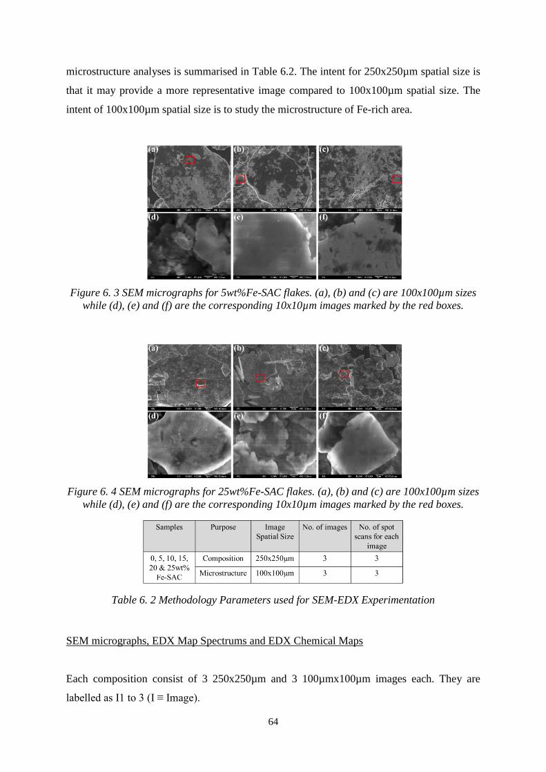
64
microstructure analyses is summarised in Table 6.2. The intent for 250x250µm spatial size is
that it may provide a more representative image compared to 100x100µm spatial size. The
intent of 100x100µm spatial size is to study the microstructure of Fe-rich area.
Figure 6. 3 SEM micrographs for 5wt%Fe-SAC flakes. (a), (b) and (c) are 100x100µm sizes
while (d), (e) and (f) are the corresponding 10x10µm images marked by the red boxes.
Figure 6. 4 SEM micrographs for 25wt%Fe-SAC flakes. (a), (b) and (c) are 100x100µm sizes
while (d), (e) and (f) are the corresponding 10x10µm images marked by the red boxes.
Table 6. 2 Methodology Parameters used for SEM-EDX Experimentation
SEM micrographs, EDX Map Spectrums and EDX Chemical Maps
Each composition consist of 3 250x250µm and 3 100µmx100µm images each. They are
labelled as I1 to 3 (I ≡ Image).

65
BM SAC305:
Figure 6. 5 250x250µm I1
Figure 6. 6 250x250µm I2

66
Figure 6. 7 250x250µm I3
Figure 6. 8 100x100µm I1

67
Figure 6. 9 100x100µm I2
Figure 6. 10 100x100µm I3

68
5wt%Fe-SAC:
Figure 6. 11 250x250µm I1
Figure 6. 12 250x250µm I2
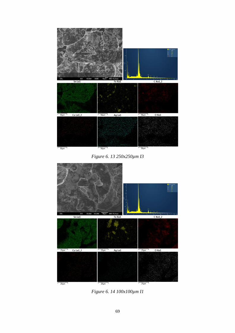
69
Figure 6. 13 250x250µm I3
Figure 6. 14 100x100µm I1

70
Figure 6. 15100x100µm I2
Figure 6. 16 100x100µm I3

71
10wt%Fe-SAC:
Figure 6. 17 250x250µm I1
Figure 6. 18 250x250µm I2
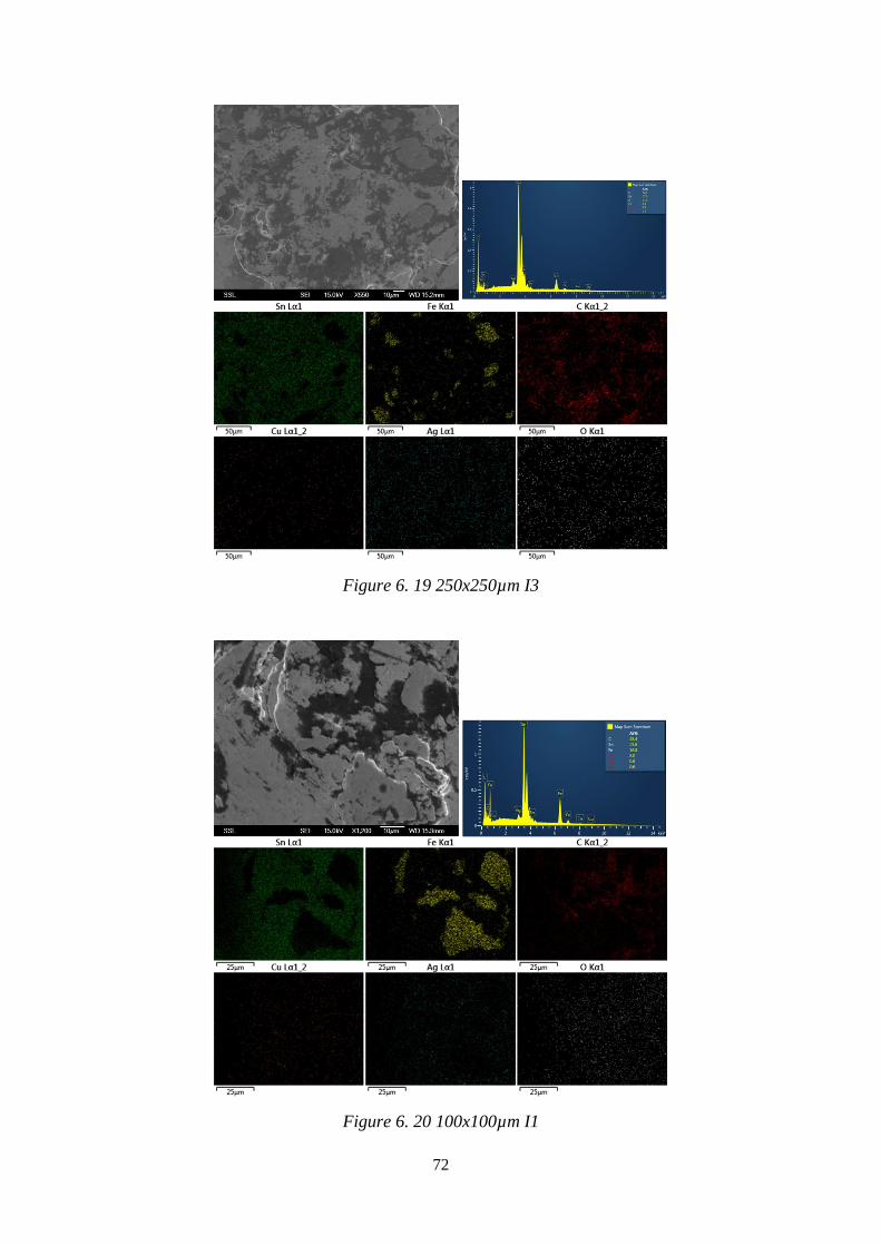
72
Figure 6. 19 250x250µm I3
Figure 6. 20 100x100µm I1
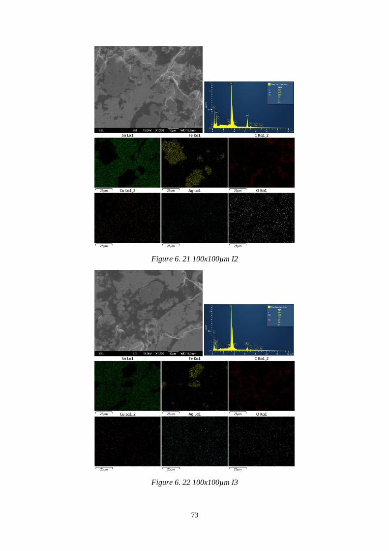
73
Figure 6. 21 100x100µm I2
Figure 6. 22 100x100µm I3

74
15wt%Fe-SAC:
Figure 6. 23 250x250µm I1
Figure 6. 24 250x250µm I2
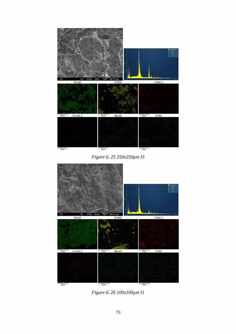
75
Figure 6. 25 250x250µm I3
Figure 6. 26 100x100µm I1

76
Figure 6. 27 100x100µm I2
Figure 6. 28 100x100µm I3

77
20wt%Fe-SAC:
Figure 6. 29 250x250µm I1
Figure 6. 30 250x250µm I2

78
Figure 6. 31 250x250µm I3
Figure 6. 32 100x100µm I1

79
Figure 6. 33 100x100µm I2
Figure 6. 34 100x100µm I3

80
25wt%Fe-SAC:
Figure 6. 35 250x250µm I1
Figure 6. 36 250x250µm I2

81
Figure 6. 37 250x250µm I3
Figure 6. 38 100x100µm I1
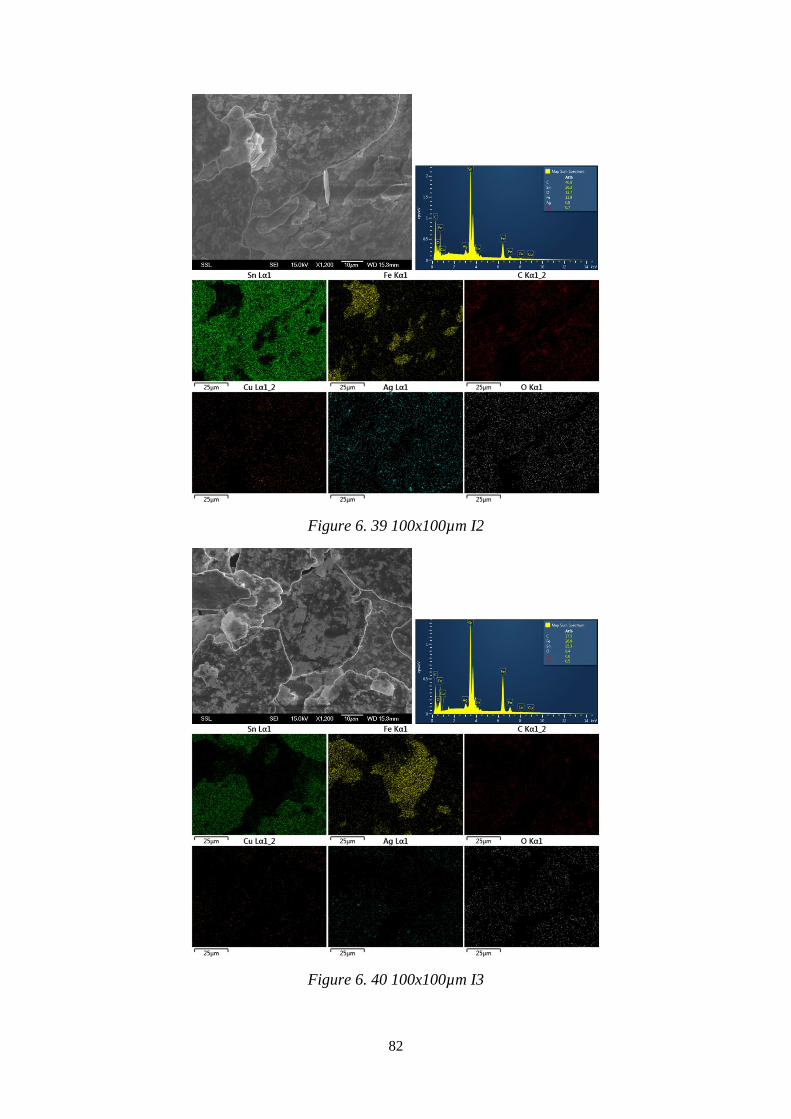
82
Figure 6. 39 100x100µm I2
Figure 6. 40 100x100µm I3

83
6.3 Appendix III: Calculated Expected Values of Saturation
Magnetization for Fe-SAC305 system
Table 6. 3Experimental and expected values of saturation magnetization from VSM result
6.4 Appendix IV: Miscellaneous DSC Experimental Results
Experimental data for Stearic Acid
Figure 6. 41 DSC curves of Stearic Acid 1st, 2nd and 3rd heating.
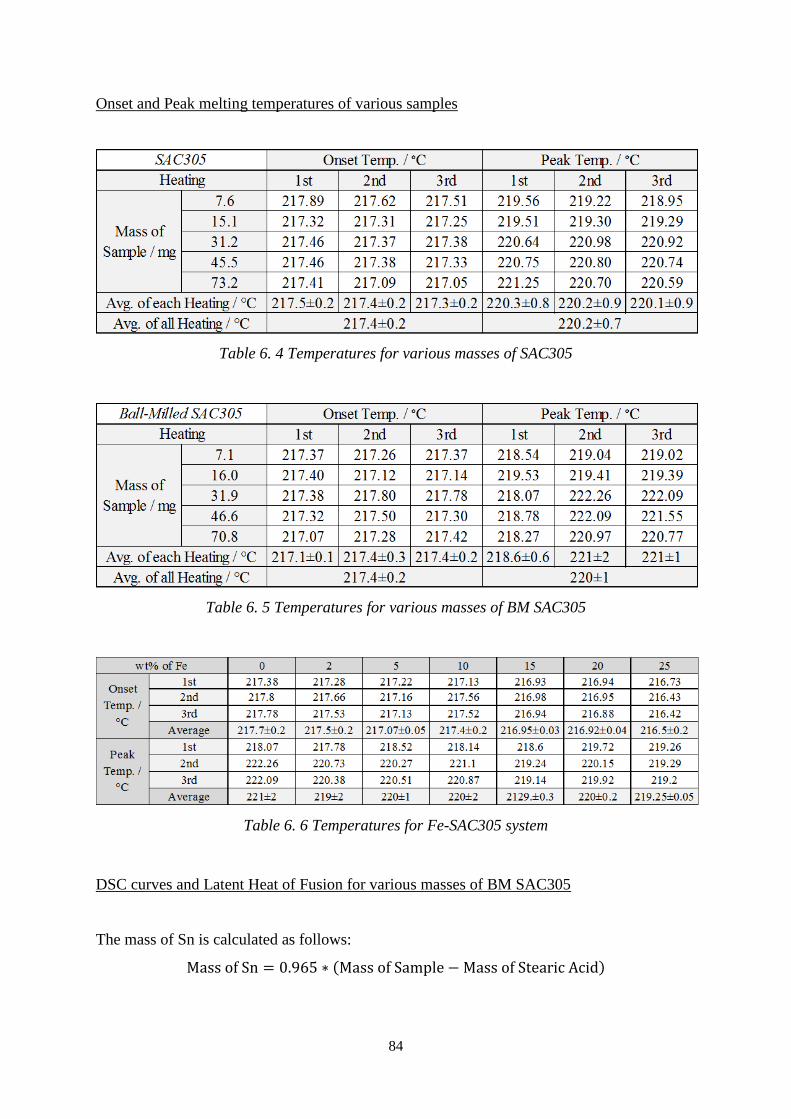
84
Onset and Peak melting temperatures of various samples
Table 6. 4 Temperatures for various masses of SAC305
Table 6. 5 Temperatures for various masses of BM SAC305
Table 6. 6 Temperatures for Fe-SAC305 system
DSC curves and Latent Heat of Fusion for various masses of BM SAC305
The mass of Sn is calculated as follows:
Mass of Sn = 0.965 ∗ (Mass of Sample − Mass of Stearic Acid)

85
.
Figure 6. 42 (a), (c) and (e) DSC curves of 1st, 2nd and 3rd heating respectively for 5
different sample masses. (b), (d) and (f) plots of Latent Heat of Fusion against Mass of Sn for
1st, 2nd and 3rd heating respectively. Curves are vertically displaced by -15 mW p

86
Absolute experimental values of latent heat of fusion
Table 6. 7 BM SAC305 for 1st, 2nd and 3rd heats
Table 6. 8 Fe-SAC305 system for 1st, 2nd and 3rd heats
6.5 Appendix V: Solder Joint Features
Zoom in on solder joint features
Figure 6. 43 Cu pads peeling at area without solder joints

87
Figure 6. 44 Black spots in interfacial regions and solder bulk
Figure 6. 45 Close up of 7 Cu pads for BM-SAC305

88
Figure 6. 46 Close up of 7 Cu pads for 25wt%Fe-SAC
Figure 6. 47 Some solder bulks which appear detached from Cu pads. Thin red arrows show
solder bulks with no IMCs observed. Thick dotted blue arrows show solder bulks with IMCs
observed.

89
Figure 6. 48 Rectangular features which may be Ag3Sn platelets
6.6 Appendix VI: IMC Measurement Methodology
Two IMC measurement methodologies were commonly harnessed: (a) Average Height and
(b) Area/Length methodologies with equations as follows:
(a) IMC thickness =1
N∑ HN
1 [66, 67]
(b) IMC thickness =IMC area
length in x direction [68, 69]
Figure 6. 49 IMC thickness measurement methodology (a) average height and (b)
area/length methodologies
From Lin. (2014), both methodologies give similar results. As shown in Fig. 6.50, the two
methodologies were used in IMC measurement and the results are compared in Table 6.9. 3
length in x directions were used.

90
Figure 6. 50 Both methodologies used to measure IMC thickness with x length of 30µm,
70µm and 100µm.
Table 6. 9 Results from both methodology
Methodology (b) is always larger than (a) as some IMCs grow sloping to one side.
Methodology (b) was harnessed in the measurement of the IMC thickness in this thesis with
length of 70µm due to limited x length of interfacial IMCs.
6.7 Appendix VII: Calculated Values of Induction Heating Time
Table 6. 10 Induction heating time between frequency range of 10kHz to 600kHz