imaging carbon materials with correlative raman...
TRANSCRIPT

Application Example
www.tescan.com
Carbon materials are widely used in many industries for their exceptional properties. Electric conductance, light weight,
strength, thermal resistance and other attributes are all available in different allotropes of one element - Carbon (diamond,
graphite, graphene, etc.). All of these materials consist of pure carbon and have only C-C bonds, which is ideal for Raman
spectroscopy. Moreover, Raman spectroscopy has the ability to differentiate small orientation changes in these bonds.
Therefore, Raman spectroscopy has the potential to not only discriminate among these allotropes but it can also identify
structural damage, or deviations and even different inner stresses.
Imaging Carbon materials with correlative Raman-SEM microscopy
IntroductionCorrelation of this powerful technique with a scanning electron microscope (SEM) is beneficial in many ways. First of all, it achieves the required magnification and resolution for detailed observation of carbon materials such as fullerene clusters, carbon nanotubes (CNT), nanocrystalline diamond (NCD) or graphene. Additional analytical methods such as EDX can be used to obtain elemental mappings of
these materials with a focus on impurities or contamination. Moreover, the use of the Focused Ion Beam (FIB) technique has become a standard tool in FIB-SEMs for excavation and 3D reconstruction of defects hidden underneath the sample surface. One of many such examples is the 3D reconstruction of cracks in dia-mond layers on cutting tools.
Raman, SEM and FIB within one chamberMounting a Confocal Raman Microscope (CRM) onto a FIB-SEM chamber allows the transfer of an area of interest from SEM to CRM and back with a single click. It saves a lot of time because the transfer between the two standalone instruments is thus avoided. This in-situ process also avoids the exposure of the sample to the ambient air which prevents it from oxidation.In the RISE (Raman Integrated Scanning
Electron) microscope, an area of interest is chosen through SEM with magnifications ranging from 20x up to 1Mx and, a high resolution image is then captured. Next, with one click the sample is transferred under the optical microscope of the CRM and the sample is imaged with a 100x optical objective. The area of interest is located in the optical image and Raman mapping is performed. That is all – quick and easy.
DiamondThe first of the presented carbon allo-tropes is diamond. Diamond is transparent over a very wide wavelength range. It is considered to be the hardest, the stiffest (and least compressible) material with the highest thermal conductivity
and inert to most chemical reagents. The transference of these outstanding properties onto many tools and materials is possible through the deposition of thin diamond films on many different substrates.
Application Example Imaging Carbon materials with correlative Raman-SEM microscopy
www.tescan.com
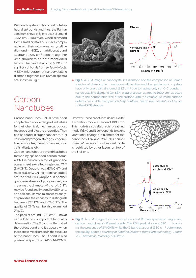
Diamond crystals only consist of tetra-hedral sp3 bonds and thus, the Raman spectrum shows only one peak at around 1332 cm-1. However, when diamond forms small crystals of surface compa-rable with their volume (nanocrystalline diamond – NCD), an additional band at around 1620 cm-1 appears together with shoulders on both mentioned bands. The band at around 1620 cm-1 signifies sp2 bonds from surface defects. A SEM micrograph of nanocrystalline diamond together with Raman spectra are shown in Fig. 1. c Fig. 1: A SEM image of nanocrystalline diamond and the comparison of Raman
spectra of diamond with nanocrystalline diamond. Large diamond crystals have only one peak at around 1332 cm-1 due to having only sp3 C-C bonds. In nanocrystalline diamond (on SEM picture) a peak at around 1620 cm-1 appears due to the comparable size of the surface with the volume, i.e. more surface defects are visible. Sample courtesy of Marian Varga from Institute of Physics of the ASCR, Prague.
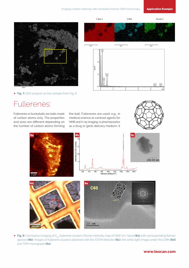
c Fig. 2: A SEM image of carbon nanotubes and Raman spectra of Single-wall carbon nanotubes of different quality. The RBM peak at around 190 cm-1 confir-ms the presence of SWCNTs while the D band at around 1330 cm-1 determines the quality. Sample courtesy of Kateřina Dědková from Nanotechnology Centre, VŠB-Technical University of Ostrava.
Carbon NanotubesCarbon nanotubes (CNTs) have been adopted into a wide range of industries for their chemical, mechanical, optical, magnetic and electric properties. They can be found in super capacitors, fuel cells and hydrogen storages, conduc-tive composites, memory devices, solar cells, displays etc.Carbon nanotubes are cylindrical tubes formed by sp2 bonded carbon atoms. A CNT is basically a roll of graphene planar sheet so-called single-wall CNT (SWCNT). Double-wall (DWCNT) and multi-wall (MWCNT) carbon nanotubes are the SWCNTs wrapped in another graphene sheets of progressively in-creasing the diameter of the roll. CNTs may be found and imaged by SEM and, an additional Raman microscopy analy-sis provides the capacity to distinguish between SW, DW and MWCNTs. The quality of CNTs can be also examined (Fig. 2).The peak at around 1330 cm-1 - known as the D band - is important for quality determination. The D band is often called the defect band and it appears when there are some disorders in the structure of the nanotubes. The D band is also present in spectra of DW or MWCNTs.
However, these nanotubes do not exhibit a vibration mode at around 190 cm-1. This mode is also called radial breathing mode (RBM) and it corresponds to slight vibrational changes in diameter of the nanotubes. DW and MWCNTs cannot “breathe” because this vibrational mode is restricted by other layers on top of the first one.

Application ExampleImaging Carbon materials with correlative Raman-SEM microscopy
www.tescan.com
c Fig. 4: An image of exfoliated graphene overlaid with Raman map shows two different areas. The corresponding spectra reveal single-layer (blue) and multi-layer (pink) graphene. In the blue spectrum, the G‘ peak is twice as tall as the G peak, which means a successful preparation of single-layer graphene.
e Fig. 3: The correlation of SEM image and Raman map of a nanocrystalline diamond layer on single-wall carbon nanotubes. Carbon nanotubes were determined by the intensity of the RBM peak at 190 cm-1 and the NCD was visualized according to the lack of RBM and the presence of both sp2
and sp3 peaks with their shoulders. Sample courtesy of Marian Varga from Institute of Physics of the ASCR, Prague.
Combined sample with NCD and SWCNTsState-of-the-art materials can be com-prised of a mixture of different com-ponents with unique properties in one advanced material. This is also the case
with mixtures of carbon allotropes. When these materials consist of pure carbon it is hard to determine their quality by means of SEM imaging and also to find
any damage caused by the preparation process. Here, we show the determination and quality check of a nanocrystalline diamond layer deposited on single-wall carbon nanotubes [1]. The transfer of the sample from SEM to Raman position and visualization of both components (Fig. 3) is done by a single click.
GrapheneGraphene is widely used because of its electrical and mechanical properties. There are several methods for graphene extraction but all these techniques have one feature in common, they aim to avoid multi-layer carbon sheets. Choosing Raman spectroscopy for the determination of the number of these layers is highly recommended.A single graphene sheet consists of
carbon bonded together by means of sp2 bonds. Looking into a number of layers, the most important is the ratio between the G (1600 cm-1) and G’ (2700 cm-1) bands in the Raman spectrum. We can identify the number of graphene layers and determine the success of making single-layer carbon sheets in both CVD graphene (Fig. 4) and exfoliated graphene (Fig. 5).

Application Example Imaging Carbon materials with correlative Raman-SEM microscopy
www.tescan.com
c Fig. 5: Overlay of SEM image and Raman map of CVD graphene (5a), Raman map (5b) and spectra (5c). The colors corre-spond to the number of layers present on the sample. The ratio between G and G‘ confirms that red area is composed of bi-layer graphene – G:G‘ = 1:1. Green and blue areas – G‘.
e Fig. 6: A SEM micrograph of ZnO on graphite correlated with an optical image and Raman map. The area in the blue frame was imaged with an optical microscope of CRM and over-laid with Raman map of the G peak intensity. The area in the red frame was correlated with another Raman map. On both Raman maps, the ZnO particles are clearly visible due to the enhancement of the signal. Sample courtesy of Kateřina Dědková from the Nanotechnology Centre, VŠB-Technical University of Ostrava.
GraphiteAnother allotrope of carbon is graphite. Graphite consists of many graphene layers. Basically the Raman spectrum looks like multi-layer graphene. The G band dominates over the G’ band. Moreover the G’ band changes its shape and becomes more complex. Graphite is used in pencils, lubricants,
etc., however, more applications of graphite are nowadays being invent-ed. For example, the combination of graphite with ZnO nanoparticles acts as a disinfection medium [2]. These ZnO/graphite microparticles were analysed with SEM, EDX and Raman spectroscopy.
5a 5b 5c
Application ExampleImaging Carbon materials with correlative Raman-SEM microscopy
www.tescan.com
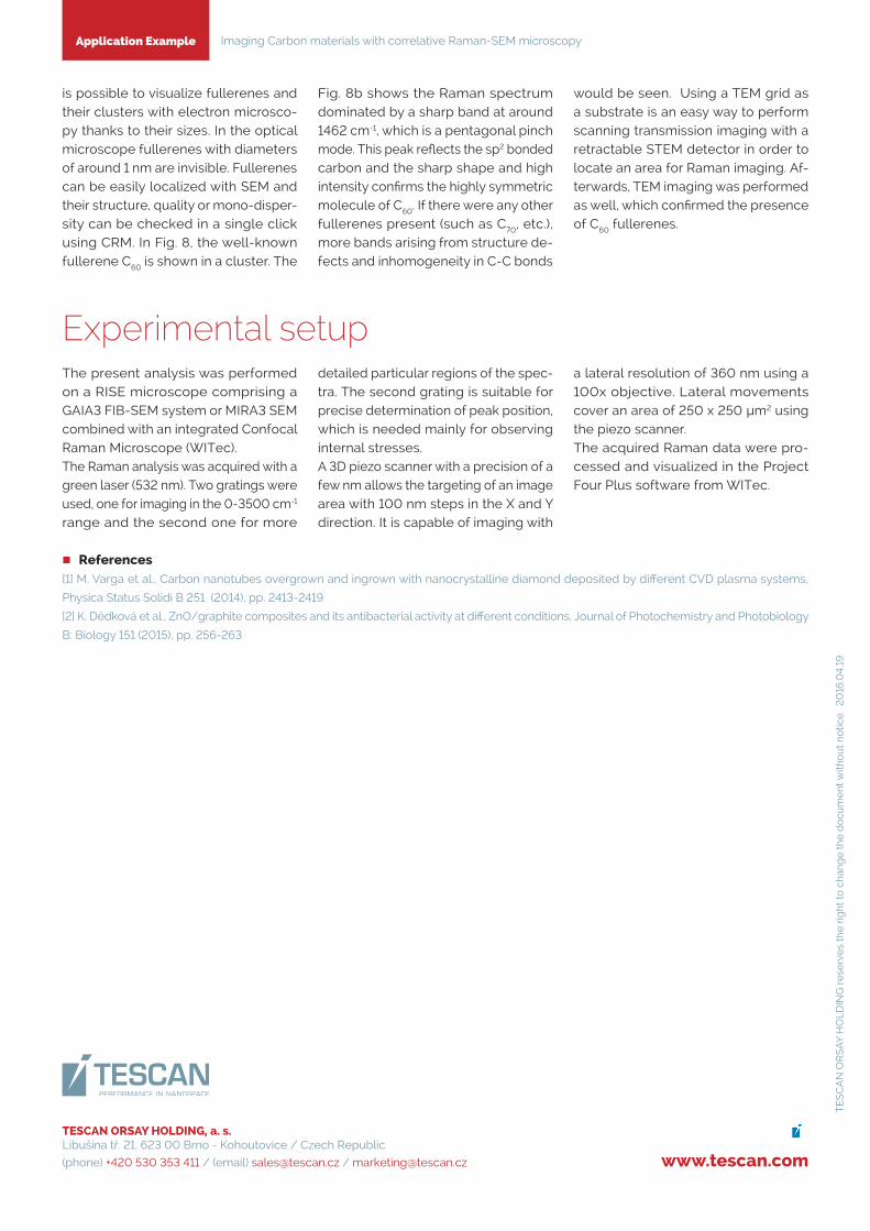
c Fig. 8: Correlative imaging of C60 fullerene clusters. Raman intensity map of 1462 cm-1 band (8a) with corresponding Raman spectra (8b). Images of fullerene clusters obtained with the STEM detector (8c), the white light image under the CRM (8d) and TEM micrograph (8e).
c Fig. 7: EDX analysis on the sample from Fig. 6.
Fullerenes:Fullerenes or buckyballs are balls made of carbon atoms only. The properties and sizes are different depending on the number of carbon atoms forming
the ball. Fullerenes are used, e.g., in medical science as contrast agents for NMR and X-ray imaging, in pharmaceutics as a drug or gene delivery medium. It
8a 8b 8c
8d 8e
TESCAN ORSAY HOLDING, a. s.Libušina tř. 21, 623 00 Brno - Kohoutovice / Czech Republic
(phone) +420 530 353 411 / (email) [email protected] / [email protected] www.tescan.com
Application Example Imaging Carbon materials with correlative Raman-SEM microscopy
is possible to visualize fullerenes and their clusters with electron microsco-py thanks to their sizes. In the optical microscope fullerenes with diameters of around 1 nm are invisible. Fullerenes can be easily localized with SEM and their structure, quality or mono-disper-sity can be checked in a single click using CRM. In Fig. 8, the well-known fullerene C60 is shown in a cluster. The
Fig. 8b shows the Raman spectrum dominated by a sharp band at around 1462 cm-1, which is a pentagonal pinch mode. This peak reflects the sp2 bonded carbon and the sharp shape and high intensity confirms the highly symmetric molecule of C60. If there were any other fullerenes present (such as C70, etc.), more bands arising from structure de-fects and inhomogeneity in C-C bonds
would be seen. Using a TEM grid as a substrate is an easy way to perform scanning transmission imaging with a retractable STEM detector in order to locate an area for Raman imaging. Af-terwards, TEM imaging was performed as well, which confirmed the presence of C60 fullerenes.
Experimental setupThe present analysis was performed on a RISE microscope comprising a GAIA3 FIB-SEM system or MIRA3 SEM combined with an integrated Confocal Raman Microscope (WITec). The Raman analysis was acquired with a green laser (532 nm). Two gratings were used, one for imaging in the 0-3500 cm-1
range and the second one for more
detailed particular regions of the spec-tra. The second grating is suitable for precise determination of peak position, which is needed mainly for observing internal stresses.A 3D piezo scanner with a precision of a few nm allows the targeting of an image area with 100 nm steps in the X and Y direction. It is capable of imaging with
a lateral resolution of 360 nm using a 100x objective. Lateral movements cover an area of 250 x 250 µm2 using the piezo scanner.The acquired Raman data were pro-cessed and visualized in the Project Four Plus software from WITec.
� References[1] M. Varga et al., Carbon nanotubes overgrown and ingrown with nanocrystalline diamond deposited by different CVD plasma systems,
Physica Status Solidi B 251 (2014), pp. 2413-2419
[2] K. Dědková et al., ZnO/graphite composites and its antibacterial activity at different conditions, Journal of Photochemistry and Photobiology
B: Biology 151 (2015), pp. 256-263
TE
SC
AN
OR
SA
Y H
OL
DIN
G r
ese
rve
s th
e r
ight
to c
han
ge
th
e d
ocu
me
nt w
itho
ut
no
tice
. 2
016
.04.
19