iit bombay-scl technology development
TRANSCRIPT
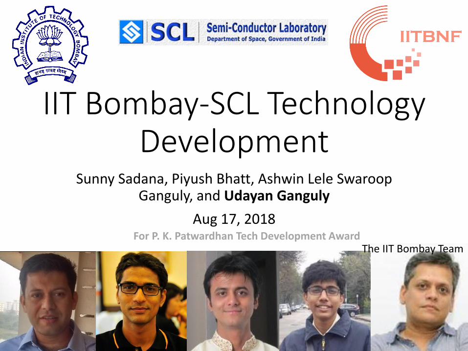
IIT Bombay-SCL Technology Development
Sunny Sadana, Piyush Bhatt, Ashwin Lele SwaroopGanguly, and Udayan Ganguly
Aug 17, 2018For P. K. Patwardhan Tech Development Award
The IIT Bombay Team
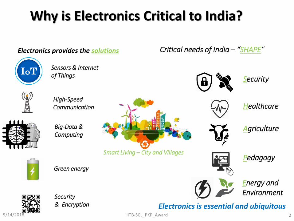
Why is Electronics Critical to India?
2
Security
Healthcare
Agriculture
Pedagogy
Energy and Environment
Critical needs of India – “SHAPE”
Smart Living – City and Villages
Sensors & Internet of Things
Big-Data & Computing
Security& Encryption
High-Speed Communication
Electronics provides the solutions
Green energy
9/14/2018 IITB-SCL_PKP_Award
Electronics is essential and ubiquitous
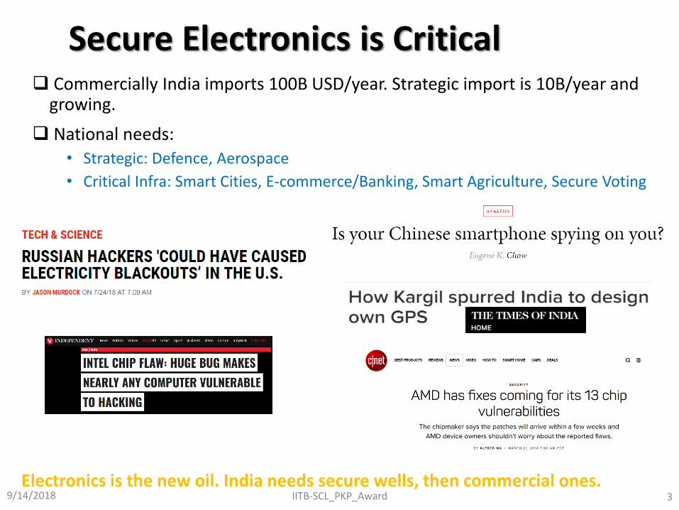
Secure Electronics is Critical Commercially India imports 100B USD/year. Strategic import is 10B/year and
growing.
National needs: • Strategic: Defence, Aerospace
• Critical Infra: Smart Cities, E-commerce/Banking, Smart Agriculture, Secure Voting
3Electronics is the new oil. India needs secure wells, then commercial ones.
9/14/2018 IITB-SCL_PKP_Award

Background & Motivation• In 2011-12, Semi-Conductor Labs Chandigarh procured a
180 nm CMOS technology fabrication unit from Tower Jazz (Israel) for 1000s of Crores
• The challenge: to address the major gaps in the offerings of the fab for high volume manufacturing (HVM)
1. BiCMOS technology (for RF based Radars & Communicat.)
2. One Time Programmable Memory (for code storage/secure memory e.g. electronic voting machines; )
3. Hardware Encryption for secure chips (e.g. banking, e-commerce etc.)
4. Multi-time Programmable Memory (for memory for secure India processor)
9/14/2018 IITB-SCL_PKP_Award 4
The goal is to develop strategic semiconductor technologies indigenously for HVM

Security Key Risk vs. H/W key solution • Soft ware keys are used for
encryption/ authentication.
• These keys are generated by vendors or programs
• Accessible by govt./ operators etc.
9/14/2018 IITB-SCL_PKP_Award 5
Intruder gets key access No external
agent is aware of private key as it is PUF based
• Solution: A PUF based hardware key is such that
• Key is auto-generated internally by the chip
• Mask independent i.e. same mask will produce random keys i.e. “unique fingerprints” the hardware
• Unreadable externally
software encryption hardware encryption

OTP Technology Basics
9/14/2018 IITB-SCL_PKP_Award 6
Metal 1
Metal 2
𝐻𝑓𝑂2
High resistance before break down
Metal 1
Metal 2
𝐻𝑓𝑂2 Co
nd
uct
ing
Fila
me
nt
Low resistanceafter break down
The challenge is (a) breakdown within supply voltage (3.3V) (b) no further breakdown during operation (1.5V TDDB etc.)
I
V
A Metal – oxide – metal capacitor is used for 2 resistance states.
Breakdown process analog is lightening
Fundamentally stochastic
VDD
𝑆𝐴
Gnd
Gnd
Selected
Un
sele
ct
𝑆𝐴 𝑆𝐴
Wordline
Bitline
A simple array is made to read and write bits
01011110001010010 : Random bits

Identical Metal Insulator Metal (MIM) Device
+
-V
Vo
ltag
e
time
Cu
rren
t
time
They have some initial atomic scale defects (e.g. missing atoms) –which are stochastic – hence atomistically non-identical
Both are macroscopically identical in size, shape and material,
9/14/2018 IITB-SCL_PKP_Award 7

A Current Flow Generated Defects
+
-V
Vo
ltag
e
time
Cu
rren
t
time
The electrons flowing through the oxide, it disturbs atomic arrangements further; some bonds break stochastically to dislodge atoms permanently to produce defects.
If a voltage is applied, current flow.
9/14/2018 IITB-SCL_PKP_Award 8

A conducting filament produces a short
+
-V
Vo
ltag
e
time
Cu
rren
t
time
When defects align to form a continuous path, a filament is formed.
Suddenly, when the filament is formed at time t1, the devices shorts and a large current flows; This is the low resistance state or logical “0”;
t1
9/14/2018 IITB-SCL_PKP_Award 9
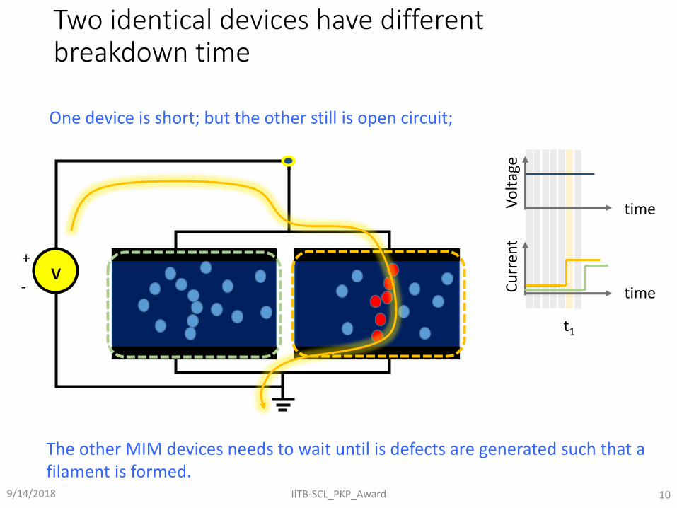
Two identical devices have different breakdown time
+
-V
Vo
ltag
e
time
Cu
rren
t
time
t1
The other MIM devices needs to wait until is defects are generated such that a filament is formed.
One device is short; but the other still is open circuit;
9/14/2018 IITB-SCL_PKP_Award 10
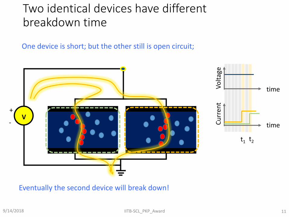
Two identical devices have different breakdown time
+
-V
Vo
ltag
e
time
Cu
rren
t
time
t1 t2
One device is short; but the other still is open circuit;
Eventually the second device will break down!
9/14/2018 IITB-SCL_PKP_Award 11

A distribution of breakdown time
Vo
ltag
e
time
Cu
rren
t
time
t1 t2
When many (say 1000) devices are tested, each device breaks down at different times; For identical devices, the breakdown occurs at different times;
Cu
mu
lati
ve D
istr
ibu
tio
n
time0%
100%
50%
A cumulative distribution can be plotted;
t1 t2
9/14/2018 IITB-SCL_PKP_Award 12

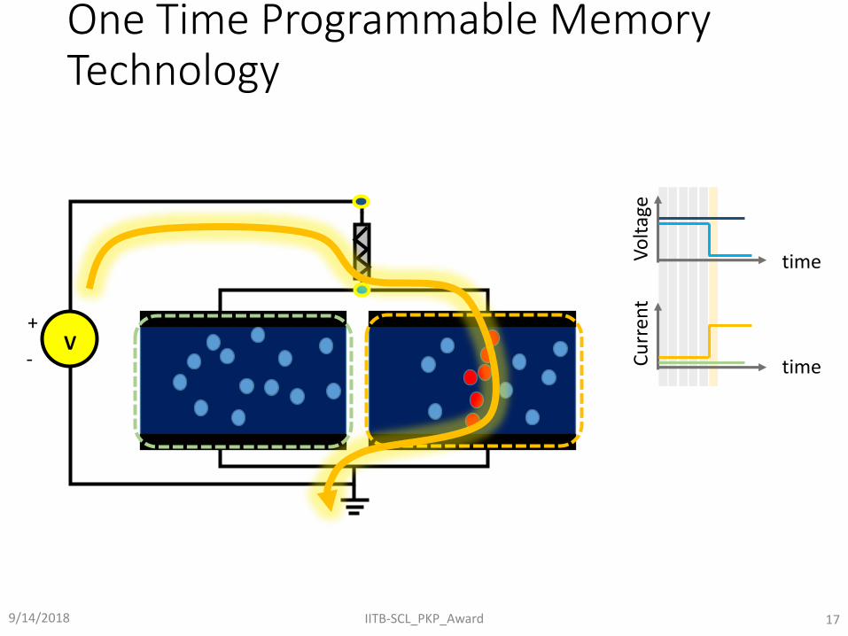
Application 1: One Time Programmable Memory Technology
Vo
ltag
e
time
Cu
rren
t
time
t1 t2
Given a t𝑝𝑢𝑙𝑠𝑒 = tMEM where P=100%; then 100% is short (“0”);
Short“0”
A memory technology requires that a MIM device be deterministically programmed to “0” ; Apply a high bias guarantees breakdown.
Cu
mu
lati
ve D
istr
ibu
tio
n
time0%
100%
50%
t1 t2
Open“1”
tMEM
9/14/2018 IITB-SCL_PKP_Award 13
Thus, we can program a bit with certainty!

tRNG
Application 2: Physical UnclonableFunction (PUF) Technology for chip ID
Vo
ltag
e
time
Cu
rren
t
time
t1 t2
It’s a Random Number Generator
A chip ID requires a random barcode spontaneously generated (no one controls this) It is perfectly random; Hence completely unpredictable!
Short“0”
Cu
mu
lati
ve D
istr
ibu
tio
n
time0%
100%
50%
t1 t2
Open“1”
tMEM
Given a t𝑝𝑢𝑙𝑠𝑒 = tRNG where P=50%; then 50% devices will be open (“1”) and 50% is
short (“0”); However, it is impossible to guess, which ones.
9/14/2018 IITB-SCL_PKP_Award 14
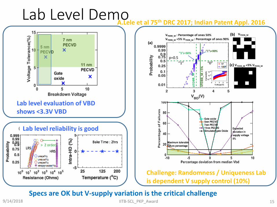
Lab Level Demo
Lab level reliability is good
Lab level evaluation of VBD shows <3.3V VBD
Specs are OK but V-supply variation is the critical challenge9/14/2018 IITB-SCL_PKP_Award 15
Challenge: Randomness / Uniqueness Lab is dependent V supply control (10%)
A.Lele et al 75th DRC 2017; Indian Patent Appl. 2016

One Time Programmable Memory Technology
+
-V
Vo
ltag
e
time
Cu
rren
t
time
9/14/2018 IITB-SCL_PKP_Award 16
One Time Programmable Memory Technology
+
-V
Vo
ltag
e
time
Cu
rren
t
time
9/14/2018 IITB-SCL_PKP_Award 17

One Time Programmable Memory Technology
+
-V
Vo
ltag
e
time
Cu
rren
t
time
9/14/2018 IITB-SCL_PKP_Award 18

Tech 1: OTP & Tech 2: PUF Demonstration at SCL
9/14/2018 IITB-SCL_PKP_Award 19
V-supply variation tolerance
“0” “1”
Memory window at 25°C
Memory States are digital
>104
20 25 30 35 40 45 50 55 60 65 70 75 80
Inter HD(%)
05
1015202530354045
Occ
ure
nce
s(%
) PUF - SCL
Simulation for p=0.5
25 175 250
Temperature(oC)
-5
0
5
Intr
a-H
D(
%)
Perfectly stochastic (patent)Unbiased RNGNIST Tested
Extreme thermal stability
6 hrs bake
0% bits flipped after Temp stress
OTP PUF Tech. DRDO PUF ASIC
• Various specs
Team1. Fab (SCL)2. Tech (IITB): 3. Circuit (IITD)4. User (DRDO-PSA)

BJT for BiCMOS
OTP Memory
Hardware Encryption
Flash Memory
Achievement: Four Tech at 180 nm node in 2 years
9/14/2018 IITB-SCL_PKP_Award 20
0 2 4 6 8 10 12 14 16 180
20
40
60
80
100
120
140
Vceo
= 5V
Baseline
Condition1
Condition2
Condition3
Condition4
hfe
Vceo (V)
hfe = 50 16X
Experiments meet spec with 16x improvement
20 25 30 35 40 45 50 55 60 65 70 75 80
Inter HD(%)
05
1015202530354045
Occ
ure
nce
s(%
) PUF - SCL
Simulation for p=0.5
Perfectly stochastic h/wUnbiased RNG (cf. coin)NIST Test Passed
101
102
103
P/E Cycles(#)
6
6.5
7
7.5
8
8.5
VF
B (
V)
VFB
Erase
VFB
Prog
P/E : 25V/-20V 10ms
Memory
Window
> 1V
Excellent Performance & reliability
OTP: Large Memory Margin
>104 ×
Excellent Performance & reliability
Multiple (1000) cycles exceeds spec
BJT for BiCMOS
Perfect Unbiased Randomness (Patent)
Demo in Manufacturing FabPlus 2 patents; 3 Conference; 1 Journal

List of Impact• July 2017: SCL has invited proposals from IITB on HBT Tech Dev (5 Crores)
• March 2018: IIT Bombay won a 50 Crore NNETRA proposal essential for CEN/IITBNF sustenance (2/4 deliverable related to IITB-SCL
• May 2018: ISRO Chairman Dr. Sivan has promised Tech Park engagement & ISRO-level committee to leverage in part IITB-SCL Tech Development
• Jun 2018: IIT Bombay is the coordinator for Strategic Nano-electronics @NNETRA
• Jun 2018: Principal Scientific Advisor’s Office & DRDO has approved Encryption Chip Technology Project (5 Cr) with IIT B as Lead of a team of IITB-IITD-SCL-SETS
• Jun 2018: NITI Aayog Dr VK Saraswat requested a R&D Foundry proposal around national technology development lead by IIT Bombay (~1000 Crores)
9/14/2018 IITB-SCL_PKP_Award 21
Significant funding and focus from strategic agencies on IITB Nanoelectronics

IP and Papers
PatentsTwo patents have been filed for OTP devices which is state of the art.
• U. Ganguly, S. Sadana, A. Lele, “Method of generating controllably biased random number by OTP devices” (Application No. 201821010427)
• P. Kumbhare, S. Sadana, U. Ganguly “One Time Programmable Memory for Encryption and Reconfigurable Circuits”” (Application No. 201621031483)
Publication• S. Sadana, A. Lele, S. Tsundus, P.
Kumbhare, U. Ganguly”A Highly Reliable and Unbiased PUF based on Differential OTP memory” IEEE Electron Devices Letters 2018
• Piyush Bhatt, Amit Kumar Singh, Monika Gupta, B.Umapathi, HS Jatana and U.Ganguly “Technology development of CMOS compatible high gain BJT to enable 180nm BiCMOS technology”International Workshop on The Physics of Semiconductor Devices (IWPSD 2017).
• S. Sadana, A. Singh, D. Sehgal, B. Umapathi, H.S. Jatana, U. Ganguly “One Time Programmable (OTP) Memory based on MIM dielectric breakdown for 180nm CMOS” International Workshop on The Physics of Semiconductor Devices (IWPSD) 2017.
• Lele, S. Sadana, A. Singh, H.S. Jatana, U. Ganguly “A simple PECVD SiO2 OTP Memory based PUF for 180nm Node for IoT ” 75th Device Research Conference, 2017. link
9/14/2018 IITB-SCL_PKP_Award 22
Ideas are cutting edge concept published in top IEEE Conf & Journals

Testimonials &News
9/14/2018 IITB-SCL_PKP_Award 23
Strong appreciation from stakeholders and attention from media!

The Team & Acknowledgements
9/14/2018 IITB-SCL_PKP_Award 24
The Semi-Conductor Labs Chandigarh TeamSERB; DST-IRHPA; MeitY, IIT Bombay Start Up Grant
The IIT Bombay Team
Pratiksha Malviya, Akash Sharma, Avinash Singh, Deep Sehgal, AnujChawla, Charanjeet Singh, Amit Kumar Singh, Monika Gupta, Dr Ravi Shankar, Saahil Singla, Dr. Umapathi, H.S. Jatana and others!