iii-v selective area growth on si: from logic to photonic...
TRANSCRIPT

CONFIDENTIAL – INTERNAL USE
III-V Selective Area Growth on Si: from Logic to Photonic devices
Clement Merckling, Principal Member of the Technical Staff, imec

CONFIDENTIAL – INTERNAL USE
Introduction & motivations

CONFIDENTIAL – INTERNAL USE
“Internet of everything” revolutionThe role of the transistor
https://www.ncta.com/platform/industry-news/infographic-the-growth-of-the-internet-of-things/
Internet of everything
Introduced new devices to enable system optimization
& specializations
Ability to innovate & co-integrate devices to optimize
performance & functionality is key
New devices
Ultra-low power
Increased performance at constant leakage
Increased performance at constant power density
Sensors
Smart Mobile
Devices
Data Centers
& Servers
3

CONFIDENTIAL – INTERNAL USE
The promise of III-V semiconductors
4
Monolithic integration of III-V lasers on Si
Z. Wang et al., Nature Photonics 2015.
CMOS applications
N. Waldron et al., IEDM, 2015.
X. Zhou et al., VLSI 2014.
RF/power applications
D.-H. Kim et al., VLSI, 2012. D.S. Green et al., 2014.

CONFIDENTIAL – INTERNAL USE
III-V selective area growth challenges

CONFIDENTIAL – INTERNAL USE
Challenges of III-V heteroepitaxy on Si
Lattice mismatch
Mismatch stress relaxationMisfit dislocations at interface
Threading dislocations in the layer
Defects at interfaces or during epitaxyTwins
Stacking faults
Polar/non-polar interfacesAnti-phase boundaries (APB)
Interdiffusion at heterogeneous interfacesGroup IV/Group III-V interface
Dopants (Mg, C, S, Se, ...) interdiffusion
6
12%8% 20%4%
Dislocation(s)
Twins
Stacking fault Anti-phase
boundary
Monoatomic step
Ge
InP
Si

CONFIDENTIAL – INTERNAL USE
Challenges of III-V selective area growth
7
Perpendicular view Parallel view
Defects can’t be trapped along the trench
[110]
Efficient necking effect with side wall
[110]

CONFIDENTIAL – INTERNAL USE
InP nucleation on {111}Si V-surface
Evolution of InP SAG step-by-step
Complex nucleation process
V-shape & lattice mismatch f = 8%
8
W = 40nm
V-grooved trenches

CONFIDENTIAL – INTERNAL USE
InP nucleation on {111}Si V-surface
Evolution of InP SAG step-by-step
Complex nucleation process
V-shape & lattice mismatch f = 8%
9
W = 40nm
Nucleation / Islanding (high density)
Coalescence
Rough / 3D growth
2D growth
Epitaxial process

CONFIDENTIAL – INTERNAL USE
InP nucleation on {111}Si V-surface
Evolution of InP SAG step-by-step
Complex nucleation process
V-shape & lattice mismatch f = 8%
10
W = 40nm
Nucleation / Islanding (high density)
Coalescence
Rough / 3D growth
2D growth
Epitaxial process

CONFIDENTIAL – INTERNAL USE
InP nucleation on {111}Si V-surface
Evolution of InP SAG step-by-step
Complex nucleation process
V-shape & lattice mismatch f = 8%
11
W = 40nm
Nucleation / Islanding (high density)
Coalescence
Rough / 3D growth
2D growth
Epitaxial process

CONFIDENTIAL – INTERNAL USE
InP nucleation on {111}Si V-surface
Evolution of InP SAG step-by-step
Complex nucleation process
V-shape & lattice mismatch f = 8%
Uniform growth obtained in sub-50nm
trenches
12
W = 40nm
Nucleation / Islanding (high density)
Coalescence
Rough / 3D growth
2D growth
Epitaxial process

CONFIDENTIAL – INTERNAL USE
“State of the art” InP/Si
(111) facetted InP during growth
and above STI level
Very low {111} defects density
along the trenches
13
W=50nm
W=50nm
W=50nm
100nm Si
InP
C. Merckling et al., J. Appl. Phys. (2014)

CONFIDENTIAL – INTERNAL USE
III-V SAG process scalability
14
W=
30n
m
Tre
nch
wid
th
W=
20n
mW
=15n
m
Very low {111} defects density along the trenches

CONFIDENTIAL – INTERNAL USE
X-Ray diffraction of InP/Si
Intense InP (004) Bragg reflection
Low Rocking curve FWHM = 450 arcsec
Fully relaxed InP layer from (224) RSM
15
-5000 0 5000
102
103
104
(arcsec)
-scan
450 arcsec
250nm
10 % active
InP
Si(2 2 4)
-14000 -12000 -10000 -8000 -6000 -4000 -2000 0 20001E-6
1E-5
1E-4
1E-3
0.01
0.1
1
Inte
nsi
ty (
arb. units)
- 2 (arcsec)
(0 0 4)
InP
Si
C. Merckling et al., J. Appl. Phys. (2014)

CONFIDENTIAL – INTERNAL USE
Crystallinity depth profile
Depth analysis of InP crystal quality by RBS
channeling along <001> axis
Si/InP interface showed high χmin up to 30%
χmin is decreasing along InP thickness reaching
minimal value of 7%
χmin of InP(001) is ~ 5%
Very high InP crystalline quality on
Si(001)
16
0100
200
0
10
20
30
40
50
X(t)
Dis
tan
ce fr
om
su
rfa
ce
χmin

CONFIDENTIAL – INTERNAL USE
in-situ InGaAs / InP / Si(001)
Defect density control in III-V buffer is THE KEY !!!17
InGaAs line
InP
SiSi
InP
InGaAs
CONFIDENTIAL – INTERNAL USE
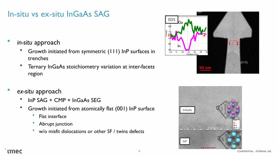
In-situ vs ex-situ InGaAs SAG
in-situ approach
Growth initiated from symmetric (111) InP surfaces in
trenches
Ternary InGaAs stoichiometry variation at inter-facets
region
ex-situ approach
InP SAG + CMP + InGaAs SEG
Growth initiated from atomically flat (001) InP surface
Flat interface
Abrupt junction
w/o misfit dislocations or other SF / twins defects
18
5 nm5 nm5 nm5 nm5 nm
InGaAs
InP
interface
IGA
dum
bbells
InP
dum
bbells
50 nm
1 2
Position (nm)
Counts
302520151050.0
160
140
120
100
80
60
Ga
1
EDS
In
2
(111)

CONFIDENTIAL – INTERNAL USE
From “planar” to vertical devices
Scaling Vertical architecture
Electrostatics Gate-All-Around
Performance High mobility III-V19
Contact-to-Gate
space
Lgate
141075
10
40
60
90
Ph
ysi
cal
Dim
en
sio
n (
nm
)
CMOS Technology Node (nm)
Self-Aligned
Contact
No room for
lateral CPP
(=2D layout)
vertical ?
?
STI
Gate
Si
STI
GAA FinFET Planar bulk FET
Contacted Gate Pitch
“Planar”Vertical
III-
V
III-
V
III-
V
Silicon
Metal
High-
Channel

CONFIDENTIAL – INTERNAL USE
III-V VFET options
“Top – Down”
Blanket growth of III-V heterostucture
Etched NWs
“Bottom – Up”
Pattern definition with narrow holes as active area
III-V NWs SAG
20
Si(111)
III-
V
SiO2
Top-down
EPI + etchBottom-up
SAG
Si(111)
SiO2
<001> <111>{111}
defects
APB
+
{111}
defects
Etch NWs SAG NWs
Substrate Si(001) Si(111)
Channel
orientation
<001> <111>
Defects {110} vertical
{111} inclined
{111} planar
Hobbs et al., Chem. Mater., 2012, 24 (11), pp 1975–1991

CONFIDENTIAL – INTERNAL USE
III-V vertical nanowires
Systematic study of NWs growth in
production tool
First good yield III-V NWs arrays on
200mm wafers: GaAs,
InGaAs,
InAs
High stacking fault / twins density in the In-
based wires
21
InAs
High density
of SFs
GaAs
Cubic phase
with few SFs
HRTEMSEM
InGaAs
Random SFs

CONFIDENTIAL – INTERNAL USE
Next ?
1st III-V NWs on
300mm Si(111)
substrate
22

CONFIDENTIAL – INTERNAL USE
III-V Logic Devices

CONFIDENTIAL – INTERNAL USE
III-V FinFET
1st working III-V SAG based FinFET
Poor electrostatic control
But proof of concept for SAG
approach
24
FinFET
p-doped InP(Mg) to limit substrate
leakage
InGaAs channel
RMG processing
N. Waldron et al., VLSI symp. (2014)

CONFIDENTIAL – INTERNAL USE
III-V Lateral-GAA-NWs
High electrostatic control
SSmin = 66mV/dec
25
Starting from FinFET
InP buffer etched, reducing substrate leakage
Dual-nanowires device
Sub-10nm channel diameter
10nm
N. Waldron et al., EDL (2014)
III-V
High-k
Metal

CONFIDENTIAL – INTERNAL USE
III-V Photonic Devices
CONFIDENTIAL – INTERNAL USE
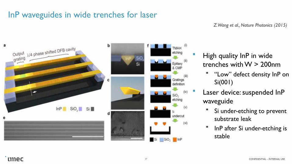
InP waveguides in wide trenches for laser
High quality InP in wide
trenches with W > 200nm
“Low” defect density InP on
Si(001)
Laser device: suspended InP
waveguide
Si under-etching to prevent
substrate leak
InP after Si under-etching is
stable
27
Z. Wang et al., Nature Photonics (2015)

CONFIDENTIAL – INTERNAL USE
RT InP DFB laser array on Si(001)
28Z. Wang et al., Nature Photonics (2015)
Optically pumped InP laser
device demonstrated on Si
Room Temperature 930nm laser
emission (FHMW < 1.6nm)
Wavelength tuning by grating
engineering (wavelength-division
multiplexing devices - WDM)

CONFIDENTIAL – INTERNAL USE
Conclusions

CONFIDENTIAL – INTERNAL USE
Conclusions
Monolithic integration of III-V compounds for advanced Logic nMOS devices &
Optical I/O Laser devices on 300mm Si platform
III-V SAG hetero-epitaxy is powerful, flexible approach
In trenches, wide to narrow CDs
From holes for vertical architecture
Fundamental understanding of III-V Selective Area Growth
InP SAG in trenches generate complex growth mode
Unique relaxation mechanism for InP{111}/Si{111}
High crystalline quality despite large mismatch with Si
Ramping up activity on vertical NWs SAG on 300mm Si(111)
Devices: nMOS and RT Lasers demonstrated on Si(001)
30

CONFIDENTIAL – INTERNAL USE31