ieee transactions on very large scale …mnikdast/files/papers/mahdi_j19.pdf · qc h3t 1j4, canada...
TRANSCRIPT

IEEE TRANSACTIONS ON VERY LARGE SCALE INTEGRATION (VLSI) SYSTEMS, VOL. 24, NO. 7, JULY 2016 2475
Coherent and Incoherent Crosstalk NoiseAnalyses in Interchip/Intrachip Optical
Interconnection NetworksLuan H. K. Duong, Student Member, IEEE, Zhehui Wang, Student Member, IEEE, Mahdi Nikdast, Member, IEEE,
Jiang Xu, Member, IEEE, Peng Yang, Zhifei Wang, Zhe Wang, Student Member, IEEE, Rafael K. V. Maeda,Haoran Li, Xuan Wang, Student Member, IEEE, Sébastien Le Beux, Student Member, IEEE, and Yvain Thonnart
Abstract— Recently, interchip/intrachip optical interconnectionnetworks have been proposed for ultrahigh-bandwidth andlow-latency communications. These networks employ themicroresonators (MRs) to modulate, direct, or detect the opticalsignal. However, utilized MRs suffer from intrinsic crosstalk noiseand signal power loss, degrading the network efficiency via thesignal-to-noise ratio (SNR). The amount of crosstalk noise andsignal power loss may differ from network to network. Hence,there exists a need to systematically analyze the effect of thecrosstalk noise and the power loss issues. In this paper, wehave developed the analytical models considering both coherentand incoherent crosstalk for both the interchip and intrachipoptical networks. The interchip/intrachip optical interconnectionnetworks—the I2CON—are analyzed as a case study. The quanti-tative results on the individual networks have demonstrated thatthe architectural design determines the impact of crosstalk on theSNR. We have also demonstrated that the optical interconnectionnetworks with interchip/intrachip interconnects result in betterbit error rate (BER) compared with that of only intrachipinterconnect. Our analyses of the worst case can be utilizedas a platform to compare the realistic performance amongdifferent optical interconnection networks via the degradationof SNR/BER and data bandwidth.
Index Terms— Bit error rate, crosstalk noise, intra/inter-chipoptical interconnection network, signal-to-noise ratio.
I. INTRODUCTION
THE International Technology Roadmap for Semi-conductors predicts that CMOS feature size will shrink
to 11 nm by 2020 [1]. As such, unprecedented quantities oftransistors will allow computer architects to integrate hundredsor even thousands of cores into a single die. With such a large
Manuscript received May 18, 2015; revised August 21, 2015 andOctober 23, 2015; accepted December 2, 2015. Date of publication January 25,2016; date of current version June 23, 2016. This work is supported by theresearch under grant GRF620911, GRF620512, and DAG11EG05S.
L. H. K. Duong, Z. Wang, J. Xu, P. Yang, Z. Wang, Z. Wang,R. K. V. Maeda, H. Li, and X. Wang are with the Department ofElectronic and Computer Engineering, The Hong Kong Universityof Science and Technology, Hong Kong (e-mail: [email protected];[email protected]; [email protected]; [email protected]; [email protected];[email protected]; [email protected]; [email protected];[email protected]).
M. Nikdast is with the École Polytechnique de Montréal, Montréal,QC H3T 1J4, Canada (e-mail: [email protected]).
S. Le Beux is with the Lyon Institute of Nanotechnology, École Centralede Lyon, Écully 69134, France (e-mail: [email protected]).
Y. Thonnart is with CEA-LETI Laboratory, Grenoble 38054, France (e-mail:[email protected]).
Color versions of one or more of the figures in this paper are availableonline at http://ieeexplore.ieee.org.
Digital Object Identifier 10.1109/TVLSI.2015.2511039
number of cores on a single die, the traditional bus-based inter-connects are predicted to face fundamental physical limita-tions. The emergence of the network-on-chip (NoC) paradigmis expected to provide adequate communication support forfuture multicore processors [2]. However, global wire delaysand energy costs do not scale down with CMOS technology.Therefore, a pure metallic-based NoC architecture still facesmajor challenges.
With the increasingly high demand for computationalperformance, NoCs have been introduced to replace thetraditional interconnects. As more applications require highercomputation power and, hence, a larger number of processingcores, the metallic interconnects of NoCs could hardly meetthe high-bandwidth and low-latency demands. Fortunately,this issue has been addressed by the optical interconnectionnetworks, with the utilization of the wavelength divisionmultiplexing (WDM) technique. By integrating a large numberof wavelengths into the network, the ultrahigh-bandwidth datacommunication can be achieved.
Hence, various optical networks with different topologieshave been proposed. Among those topologies, the ring-based optical interconnects [3]–[5] are promising with theiron-chip optical crossbars for ultrahigh on-chip bandwidth.These on-chip optical crossbars can improve the networklatency because electrical–optical/optical–electrical convertersare only needed at the end of the opened ring [3], [6]. Morerecently, the ring-based optical interconnects have covered notonly an intrachip but also an interchip communication. Thesenetworks are composed of two different interconnection parts:1) the optical intrachip for the on-chip communication and2) the optical interchip is the communication among the chips.Wu et al. [7] have proposed I2CON for such interchip/intrachipoptical interconnection networks.
However, one key issue for these WDM interchip/intrachipoptical interconnection networks is the crosstalk noise.Crosstalk noise is an intrinsic characteristic of the opticalcomponents. Depending on the architecture of the network,the crosstalk noise can be intensified among numerous opticalcomponents in various combinations. Moreover, with the pres-ence of a large number of wavelengths in one single waveguide(i.e., WDM-based), crosstalk noise from different wavelengthsmay affect the detected signal on a wavelength.
Fundamentally, the crosstalk noise can be classified intotwo types: 1) coherent crosstalk and 2) incoherent crosstalk.
1063-8210 © 2016 IEEE. Personal use is permitted, but republication/redistribution requires IEEE permission.See http://www.ieee.org/publications_standards/publications/rights/index.html for more information.

2476 IEEE TRANSACTIONS ON VERY LARGE SCALE INTEGRATION (VLSI) SYSTEMS, VOL. 24, NO. 7, JULY 2016
In this paper, we formally provide the analyses of bothcoherent and incoherent second-order crosstalk noises. Indeed,Duong et al. [8] had given a case study on the crosstalk inring-based WDM optical NoCs (ONoCs). However, it solelyfocused on incoherent crosstalk with an analysis of the datachannel and the broadcast bus in one ring-based ONoC:the Corona. Another recent work on the crosstalk noise ina WDM-based ONoC is [9], which mainly focus on theincoherent crosstalk in three different topologies: 1) mesh-based; 2) folded-torus based; and 3) fat-tree-based.
In this paper, we present a systematic study on the worstcase crosstalk noise for both the interchip and intrachipoptical interconnection networks. At the optical-circuit level,we thoroughly model the basic optical elements to analyzethe signal power loss and the crosstalk noise. Having theseanalytical models, we study the worst case situations for theinterchip/intrachip optical networks. For the interchip part, weutilize the interchip part of I2CON [7]. Regarding the intrachipinterconnect, we analyze and compare the worst case crosstalknoise in the intrachip part of I2CON and another ring-basedintrachip optical network: the Corona [3]. With this bottom–upapproach, all analytical models at the network level can betranslated into initial device-level models for verification.
Finally, numerical values of the parameters used inour analytical equations are applied. Quantitative resultsof the worst case crosstalk noise, signal power loss, andsignal-to-noise ratio (SNR) are presented. It should be notedthat our analytical models do not depend on these numericalvalues. Numerical values are applied, so that we can seethe trend as well as the scalability of the interchip/intrachipnetworks. For the intrachip network, we compare the results ofthe intrachip of I2CON with the Corona network at the samenetwork size. We also explore more on the trend of the worstcase by changing different parameters, such as the Q factorsand the passing loss. Regarding the interchip network, we alsopresent the trend of the worst case crosstalk noise and the SNRunder different values of the parameters. Based on the worstcase SNR results, we also present a comparison between theideal and real bandwidths, as well as the power needed forsending a bit of data.
The rest of this paper is organized as follows. Section IIbriefly discusses the state-of-the-art of previous works, whileSection III details our models for the basic optical elements.Section IV gives the detailed analyses of the worst case powerloss and the crosstalk noise in the interchip and intrachip opti-cal interconnection networks. Section V follows and providesour quantitative results and discussion. Finally, the conclusionis drawn in Section VI.
II. SUMMARY OF RELATED WORKS
At the device level, crosstalk noise has often been consid-ered negligible. For example, the crosstalk noise of −47.4 dBwas reported in [10] via a waveguide crossing, which consistedof three cascaded multimode structures. Another work byTsarev [11] also reported the negligible loss and the crosstalknoise. Xia et al. [12] demonstrated the optical waveguide struc-tures with compact, photonic-wire-based coupled resonators.These structures included up to 16 racetrack resonators on
Fig. 1. Basic optical elements. Injectors/switching elements.
a silicon-on-insulator (SOI) substrate and resulted in a drop-port loss of less than 3 dB. Li et al. [13] designed andfabricated a compact third-order coupled-resonator filter onthe SOI platform with focused application for on-chip opticalinterconnects. In this paper, they obtained a drop-port lossof less than 0.5 dB, an in-band throughput-port extinctionof 12 dB, and an out-of-band drop rejection of 18 dB.In addition, Xiao et al. [14] researched a multiwavelengthmicroring-based structure and reported the losses.
Nonetheless, recently, the crosstalk noise issue has beenincreasingly investigated because of its negative impact onthe network. One of the most recent works on the crosstalknoise in WDM-based ONoCs is [9], which mainly focus onthe intrachip optical networks under three different topologies:1) mesh-based; 2) folded-torus based; and 3) fat-tree-based.In this paper, we present the analyses on the first-orderincoherent crosstalk noise. Besides, Duong et al. [8] reportedthe destructive effect of incoherent crosstalk on the SNR inthe data channel and the broadcast bus of Corona ONoC.
III. CROSSTALK NOISE ANALYSES IN OPTICAL ELEMENTS
In the interconnect of Dense Wavelength-Division Multi-plexing (DWDM) optical networks, the sets of basic opticaldevices are placed in order to bridge a source processor withother destination processors. Among those optical devices,splitter and microresonators (MRs) can form different struc-tures for the interconnect. Their function is to perform lightmodulation, detection, transmission, and division. To analyzethe worst case crosstalk noise in a network, we need to firstestablish the analyses of these MRs and optical splitters.
A. Lorentzian Power Transfer Function
MRs are intensively employed to construct optical inter-connects. The MR can be coupled to two waveguides andutilized as a switching element (Fig. 1). The MR can alsobe coupled to a single waveguide, forming a modulator, ora detector to, respectively, modulate or detect the opticalsignal (Fig. 2). In general, the MR is approximated as aLorentzian power transfer function which is peaked at theMR’s resonant wavelength λ j [15], [16]. For an optical signalhaving wavelength λi , the drop-port power transfer can beexpressed as [14]
Pdrop
Pin=
(2κeκd
κ2e + κ2
d + κ2p
)2 (δ2
(λi − λ j )2 + δ2
). (1)
To simplify our analytical equations in the later stages, wedefine �(i, j) as the ratio of (Pdrop/Pin) as in (1), where λ j is

DUONG et al.: COHERENT AND INCOHERENT CROSSTALK NOISE ANALYSES 2477
Fig. 2. Basic optical elements. Modulators and detectors. (a) INACTIVE-state modulator. (b) ACTIVE-state modulator. (c) PASSING-mode detector.(d) DETECTING-mode detector.
the resonant wavelength of the examined MR, and λi is thewavelength of the examined optical signal. In (1), κ2
e and κ2d
are, respectively, the fraction of the optical power that the inputand the drop waveguide coupled into or out of the MR, whileκ2
p is the fraction of the intrinsic power losses per round-tripin the MR. Based on recent works, for an MR, κ2
e = 0.003,κ2
d = 0.001, and κ2p = 0.0025 [17]. Moreover, in (1),
the −3-dB bandwidth of 2δ is expressed as
2δ = λ j
Q(2)
where Q is the Q factor of a particular MR. We also considerthe free-spectral range (FSR) of a signal via the differencebetween λ j and λi . This difference is �(i, j) = λi − λ j =(i − j)(FSR/n), where we assume equal spacing betweentwo consecutive wavelengths, and n is the total number ofwavelengths in the network. In this paper, Q factor is setat 9000 [6] and FSR is assumed to be 62 nm [18].
B. Crosstalk Noise in the Optical Elements
In optical interconnects, crosstalk noise is an intrinsiccharacteristic of photonic devices. It is classified as coherentand incoherent. Basically, we consider the crosstalk incoherentwhen the optical propagation delay differences in the networkexceed the coherent time of the laser. Otherwise, we considerit coherent. Shen et al. [19] have proved that the coherentcrosstalk may either contribute to the noise or cause fluctu-ation in the signal power. In this paper, we show the worstcase results of the crosstalk noise, which happens when thecoherent crosstalk is treated as noise, not as signal fluctuation.In order to calculate the generated crosstalk noise, we haveutilized the Lorentzian-shape power transfer function using thenear resonance state of the Lorentzian. In our future works, wewill also consider other different methods, such as the matrixmodel.
To verify the impact of crosstalk noise in the opticalinterconnects, we utilize SNR, expressed in (3), as the ratiobetween the received signal and the crosstalk noise power atthe detectors. In (3), SNR is indeed independent of the input
TABLE I
UTILIZED PARAMETERS TABLE
signal power, since the input power of the signal power and thecrosstalk noise power cancels out each other. As mentionedbefore, the noise power in the denominator includes boththe coherent crosstalk and the incoherent crosstalk. Besidesthis, in order to facilitate the understanding of our analyticalequations, Table I provides all the notations and data usedin the analyses. The data, which are a projection toward theoptical interconnect technology in 2020, are considered fromthe recent works on Corona and Coronalike interconnectionnetworks [20]–[23]
SNR = Psignal
Pnoise. (3)
C. Optical Injectors
Injectors are the MRs coupled into two waveguides.An injector performs as a switching element to change thelight direction. Fig. 1 shows its two stages: 1) the OFF-stateand 2) the ON-state. In Fig. 1, the injector is injectingwavelength λ j .
In the OFF-state, when the MR is OFF, the signal travelstoward the through port. In this case, the signal power at thethrough port and the drop port is (4a) and (4c), respectively.Due to the imperfection of the coupling mode, a portion oflight from all the wavelengths can be leaked into the dropport. This crosstalk noise power is incoherent and denotedby (4d). Meanwhile, the crosstalk noise power at the throughport (4b) is from the signal at the add port. This crosstalk noiseis coherent if the signal from the add port and the input portare generated by the same source; otherwise, it is incoherent.Besides, (4e) is the coherent crosstalk also at the through port
Ps,T ,OFF[i ] = Li0 Pin[i ] (i = 0, 1, . . . , n − 1) (4a)
Pn,T ,OFF[ j ] = (X2
i0
)Padd[ j ] (4b)

2478 IEEE TRANSACTIONS ON VERY LARGE SCALE INTEGRATION (VLSI) SYSTEMS, VOL. 24, NO. 7, JULY 2016
Ps,D,OFF[ j ] = Li0 Padd[ j ] (i = 0, 1, . . . , n − 1) (4c)
Pn,D,OFF[i ] ={
0 (i �= j)
Xi0 Pin[i ] + ∑n−1k=0 �(k, i)Pin[k] (k �= i)
(4d)
Pn−coh,T ,OFF[i ] = (X2
i0
)Pin[i ] (i = 0, 1, . . . , n − 1). (4e)
Similarly, we can derive the equations for the injector in theON-state. In this state, the signal of wavelength λ j is directedto the drop port. Hence, the signal power and the incoherentnoise at the through port are (5a) and (5c), respectively. Otheroptical signals are directed toward the through port, and theirsignal power is denoted by (5b). For the drop port, the signalpower is (5d), while the noise is from two sources: 1) thenoise from other wavelengths (5e) and 2) the noise from theoptical signal at the add port (5f)
Ps,T ,ON[i ] = Li0 Pin[i ] (i �= j) (5a)
Ps,T ,ON[ j ] = Li1 Pin[i ] (5b)
Pn−inc,T ,ON[ j ] = Xi1 Pin[ j ] (5c)
Ps,D,ON[ j ] = Li1 Pin[ j ] (5d)
Pn,D,ON,1[ j ] =n−1∑i=0
�(i, j)Pin[i ] (i �= j) (5e)
Pn,D,ON,2[ j ] = Xi1 Padd[ j ]. (5f)
D. Optical Modulators and Detectors
Similar to injectors, modulators and detectors also followthe Lorentzian transfer function. They are formed by couplingthe MRs to a single waveguide. Fig. 2 shows different statesof the modulators and the detectors. Similar analyses can beapplied, and (6) and (7) are derived for the modulators in theINACTIVE and ACTIVE states, respectively
Pout[i ] = Lm0 Pin[i ] (i = 0 . . . n) (6){Pout[ j ] = Xm1 Pin[ j ]Pout[i ] = Lm0 Pin[i ] (i �= j).
(7)
Meanwhile, (8a) and (8b) are for photodetectors in thePASSING mode, and (9a)–(9c) are for the detectors in theDETECTING mode
Pout[i ] = Ld0 Pin[i ] (i = 0 . . . n) (8a)
Pn−inc = Xd0 Pin[ j ] +n−1∑i=0
�(i, j)Pin[i ] (i �= j) (8b)
{Pout[ j ] = Xd1 Pin[ j ]Pout[i ] = Ld0 Pin[i ] (i �= j)
(9a)
Psignal = Ld1 Pin[ j ] (9b)
Pn−inc =n−1∑i=0
�(i, j)Pin[i ] (i �= j). (9c)
Regarding the coherent crosstalk, we consider the portionof power which can be leaked out from the leaked-in powerof the MR. Equation (10a) is derived for the coherent noise
Fig. 3. Basic optical elements. Optical splitters. (a) 1 × 2 splitter.(b) 1 × 4 splitter.
in the INACTIVE-state modulators, while (10b) is for theACTIVE-state modulators
Pn−coh = (X2
m0
)Pin[ j ] + Xm0
n−1∑i=0
�(i, j)Pin[i ] (10a)
Pn−coh = (X2
m1
)Pin[ j ] + Xm1
n−1∑i=0
�(i, j)Pin[i ]. (10b)
For the coherent crosstalk noise at the detectors, we derive(11a) and (11b) for PASSING-mode and DETECTING-modedetectors, respectively
Pn−coh = (X2
d0
)Pin[ j ] + Xd0
n−1∑i=0
�(i, j)Pin[i ] (11a)
Pn−coh = (X2
d1
)Pin[ j ] + Xd1
n−1∑i=0
�(i, j)Pin[i ]. (11b)
E. Optical Splitters
Optical splitters are utilized to allocate portions of signalpower from the source to different interconnection paths.For optical interconnects with the presence of off-chip lasersource (i.e., the Corona), the optical splitters are extensivelyexploited. In this paper, we model two common types ofsplitters, including 1 × 2 and 1 × 4 power splitters. As canbe seen from Fig. 3, the light passes through the splittersand suffers from the loss of L12 or L14. Thus, (12) and (13)are, respectively, the power equations for 1 × 2 and 1 × 4splitters
Pout1 = Ls12 Pin(1 − R12) and Pout2 = Ls12 Pin R12 (12)
Pout1 = Pout2 = Pout3 = Pout4 = Ls14 Pin R14. (13)
For a 1 × 2 splitter, we consider different split ratios attwo outputs, where output 1 receives (1 − R12) and output2 receives R12 of the power from the input. For a 1 × 4splitter, we consider the same split ratio (i.e., R14) at allthe outputs. Under the scope of this paper, a negligibleamount of crosstalk noise introduced by the splitters isconsidered.
DUONG et al.: COHERENT AND INCOHERENT CROSSTALK NOISE ANALYSES 2479
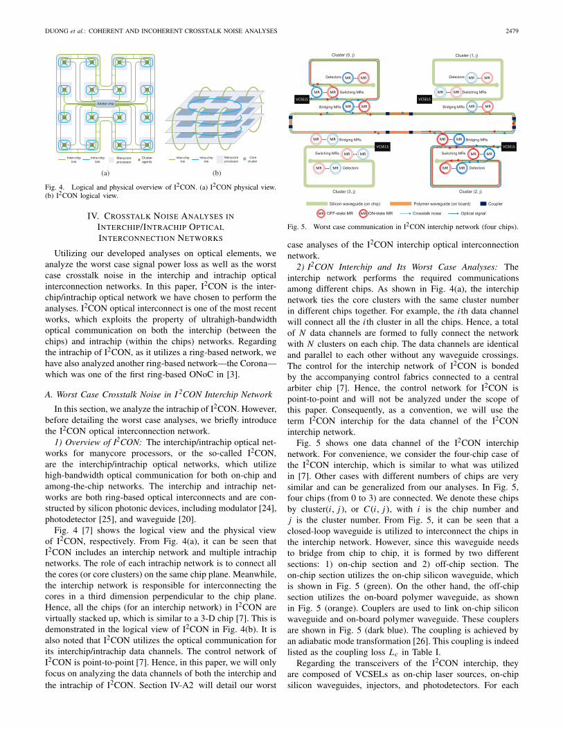
Fig. 4. Logical and physical overview of I2CON. (a) I2CON physical view.(b) I2CON logical view.
IV. CROSSTALK NOISE ANALYSES IN
INTERCHIP/INTRACHIP OPTICAL
INTERCONNECTION NETWORKS
Utilizing our developed analyses on optical elements, weanalyze the worst case signal power loss as well as the worstcase crosstalk noise in the interchip and intrachip opticalinterconnection networks. In this paper, I2CON is the inter-chip/intrachip optical network we have chosen to perform theanalyses. I2CON optical interconnect is one of the most recentworks, which exploits the property of ultrahigh-bandwidthoptical communication on both the interchip (between thechips) and intrachip (within the chips) networks. Regardingthe intrachip of I2CON, as it utilizes a ring-based network, wehave also analyzed another ring-based network—the Corona—which was one of the first ring-based ONoC in [3].
A. Worst Case Crosstalk Noise in I 2CON Interchip Network
In this section, we analyze the intrachip of I2CON. However,before detailing the worst case analyses, we briefly introducethe I2CON optical interconnection network.
1) Overview of I2CON: The interchip/intrachip optical net-works for manycore processors, or the so-called I2CON,are the interchip/intrachip optical networks, which utilizehigh-bandwidth optical communication for both on-chip andamong-the-chip networks. The interchip and intrachip net-works are both ring-based optical interconnects and are con-structed by silicon photonic devices, including modulator [24],photodetector [25], and waveguide [20].
Fig. 4 [7] shows the logical view and the physical viewof I2CON, respectively. From Fig. 4(a), it can be seen thatI2CON includes an interchip network and multiple intrachipnetworks. The role of each intrachip network is to connect allthe cores (or core clusters) on the same chip plane. Meanwhile,the interchip network is responsible for interconnecting thecores in a third dimension perpendicular to the chip plane.Hence, all the chips (for an interchip network) in I2CON arevirtually stacked up, which is similar to a 3-D chip [7]. This isdemonstrated in the logical view of I2CON in Fig. 4(b). It isalso noted that I2CON utilizes the optical communication forits interchip/intrachip data channels. The control network ofI2CON is point-to-point [7]. Hence, in this paper, we will onlyfocus on analyzing the data channels of both the interchip andthe intrachip of I2CON. Section IV-A2 will detail our worst
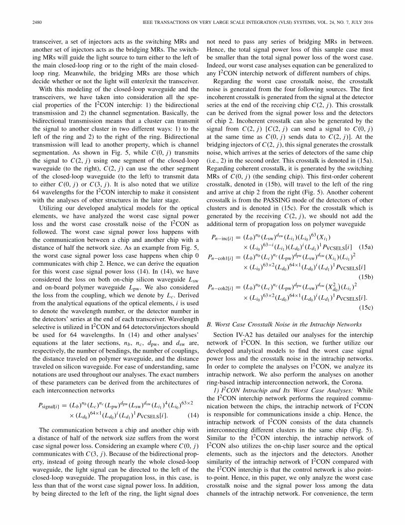
Fig. 5. Worst case communication in I2CON interchip network (four chips).
case analyses of the I2CON interchip optical interconnectionnetwork.
2) I2CON Interchip and Its Worst Case Analyses: Theinterchip network performs the required communicationsamong different chips. As shown in Fig. 4(a), the interchipnetwork ties the core clusters with the same cluster numberin different chips together. For example, the i th data channelwill connect all the i th cluster in all the chips. Hence, a totalof N data channels are formed to fully connect the networkwith N clusters on each chip. The data channels are identicaland parallel to each other without any waveguide crossings.The control for the interchip network of I2CON is bondedby the accompanying control fabrics connected to a centralarbiter chip [7]. Hence, the control network for I2CON ispoint-to-point and will not be analyzed under the scope ofthis paper. Consequently, as a convention, we will use theterm I2CON interchip for the data channel of the I2CONinterchip network.
Fig. 5 shows one data channel of the I2CON interchipnetwork. For convenience, we consider the four-chip case ofthe I2CON interchip, which is similar to what was utilizedin [7]. Other cases with different numbers of chips are verysimilar and can be generalized from our analyses. In Fig. 5,four chips (from 0 to 3) are connected. We denote these chipsby cluster(i, j ), or C(i, j), with i is the chip number andj is the cluster number. From Fig. 5, it can be seen that aclosed-loop waveguide is utilized to interconnect the chips inthe interchip network. However, since this waveguide needsto bridge from chip to chip, it is formed by two differentsections: 1) on-chip section and 2) off-chip section. Theon-chip section utilizes the on-chip silicon waveguide, whichis shown in Fig. 5 (green). On the other hand, the off-chipsection utilizes the on-board polymer waveguide, as shownin Fig. 5 (orange). Couplers are used to link on-chip siliconwaveguide and on-board polymer waveguide. These couplersare shown in Fig. 5 (dark blue). The coupling is achieved byan adiabatic mode transformation [26]. This coupling is indeedlisted as the coupling loss Lc in Table I.
Regarding the transceivers of the I2CON interchip, theyare composed of VCSELs as on-chip laser sources, on-chipsilicon waveguides, injectors, and photodetectors. For each
2480 IEEE TRANSACTIONS ON VERY LARGE SCALE INTEGRATION (VLSI) SYSTEMS, VOL. 24, NO. 7, JULY 2016
transceiver, a set of injectors acts as the switching MRs andanother set of injectors acts as the bridging MRs. The switch-ing MRs will guide the light source to turn either to the left ofthe main closed-loop ring or to the right of the main closed-loop ring. Meanwhile, the bridging MRs are those whichdecide whether or not the light will enter/exit the transceiver.
With this modeling of the closed-loop waveguide and thetransceivers, we have taken into consideration all the spe-cial properties of the I2CON interchip: 1) the bidirectionaltransmission and 2) the channel segmentation. Basically, thebidirectional transmission means that a cluster can transmitthe signal to another cluster in two different ways: 1) to theleft of the ring and 2) to the right of the ring. Bidirectionaltransmission will lead to another property, which is channelsegmentation. As shown in Fig. 5, while C(0, j) transmitsthe signal to C(2, j) using one segment of the closed-loopwaveguide (to the right), C(2, j) can use the other segmentof the closed-loop waveguide (to the left) to transmit datato either C(0, j) or C(3, j). It is also noted that we utilize64 wavelengths for the I2CON interchip to make it consistentwith the analyses of other structures in the later stage.
Utilizing our developed analytical models for the opticalelements, we have analyzed the worst case signal powerloss and the worst case crosstalk noise of the I2CON asfollowed. The worst case signal power loss happens withthe communication between a chip and another chip with adistance of half the network size. As an example from Fig. 5,the worst case signal power loss case happens when chip 0communicates with chip 2. Hence, we can derive the equationfor this worst case signal power loss (14). In (14), we haveconsidered the loss on both on-chip silicon waveguide Lswand on-board polymer waveguide Lpw. We also consideredthe loss from the coupling, which we denote by Lc. Derivedfrom the analytical equations of the optical elements, i is usedto denote the wavelength number, or the detector number inthe detectors’ series at the end of each transceiver. Wavelengthselective is utilized in I2CON and 64 detectors/injectors shouldbe used for 64 wavelengths. In (14) and other analyses’equations at the later sections, nb, nc, dpw, and dsw are,respectively, the number of bendings, the number of couplings,the distance traveled on polymer waveguide, and the distancetraveled on silicon waveguide. For ease of understanding, samenotations are used throughout our analyses. The exact numbersof these parameters can be derived from the architectures ofeach interconnection networks
Psignal[i] = (Lb)nb(Lc)
nc (Lpw)dpw(Lsw)dsw(Li1 )4(Li0 )
63×2
× (Ld0)64×1(Ld0)
i (Ld1)1 PVCSELS[i ]. (14)
The communication between a chip and another chip witha distance of half of the network size suffers from the worstcase signal power loss. Considering an example where C(0, j)communicates with C(3, j). Because of the bidirectional prop-erty, instead of going through nearly the whole closed-loopwaveguide, the light signal can be directed to the left of theclosed-loop waveguide. The propagation loss, in this case, isless than that of the worst case signal power loss. In addition,by being directed to the left of the ring, the light signal does
not need to pass any series of bridging MRs in between.Hence, the total signal power loss of this sample case mustbe smaller than the total signal power loss of the worst case.Indeed, our worst case analyses equation can be generalized toany I2CON interchip network of different numbers of chips.
Regarding the worst case crosstalk noise, the crosstalknoise is generated from the four following sources. The firstincoherent crosstalk is generated from the signal at the detectorseries at the end of the receiving chip C(2, j). This crosstalkcan be derived from the signal power loss and the detectorsof chip 2. Incoherent crosstalk can also be generated by thesignal from C(2, j) [C(2, j) can send a signal to C(0, j)at the same time as C(0, j) sends data to C(2, j)]. At thebridging injectors of C(2, j), this signal generates the crosstalknoise, which arrives at the series of detectors of the same chip(i.e., 2) in the second order. This crosstalk is denoted in (15a).Regarding coherent crosstalk, it is generated by the switchingMRs of C(0, j) (the sending chip). This first-order coherentcrosstalk, denoted in (15b), will travel to the left of the ringand arrive at chip 2 from the right (Fig. 5). Another coherentcrosstalk is from the PASSING mode of the detectors of otherclusters and is denoted in (15c). For the crosstalk which isgenerated by the receiving C(2, j), we should not add theadditional term of propagation loss on polymer waveguide
Pn−inc[i] = (Lb)nb(Lsw)dsw(Li1 )(Li0 )
63(Xi1 )
× (Li0 )63−i(Li1 )(Ld0)
i (Ld1)1 PVCSELS[i ] (15a)
Pn−coh1[i] = (Lb)nb(Lc)
nc (Lpw)dpw(Lsw)dsw(Xi1)(Li1 )2
× (Li0 )63×2(Ld0)
64×1(Ld0)i (Ld1)
1 PVCSELS[i ](15b)
Pn−coh2[i] = (Lb)nb(Lc)
nc (Lpw)dpw(Lsw)dsw(X2
d0
)(Li1 )
2
× (Li0 )63×2(Ld0)
64×1(Ld0)i (Ld1)
1 PVCSELS[i ].(15c)
B. Worst Case Crosstalk Noise in the Intrachip Networks
Section IV-A2 has detailed our analyses for the interchipnetwork of I2CON. In this section, we further utilize ourdeveloped analytical models to find the worst case signalpower loss and the crosstalk noise in the intrachip networks.In order to complete the analyses on I2CON, we analyze itsintrachip network. We also perform the analyses on anotherring-based intrachip interconnection network, the Corona.
1) I2CON Intrachip and Its Worst Case Analyses: Whilethe I2CON interchip network performs the required commu-nication between the chips, the intrachip network of I2CONis responsible for communications inside a chip. Hence, theintrachip network of I2CON consists of the data channelsinterconnecting different clusters in the same chip (Fig. 5).Similar to the I2CON interchip, the intrachip network ofI2CON also utilizes the on-chip laser source and the opticalelements, such as the injectors and the detectors. Anothersimilarity of the intrachip network of I2CON compared withthe I2CON interchip is that the control network is also point-to-point. Hence, in this paper, we only analyze the worst casecrosstalk noise and the signal power loss among the datachannels of the intrachip network. For convenience, the term

DUONG et al.: COHERENT AND INCOHERENT CROSSTALK NOISE ANALYSES 2481
Fig. 6. Worst case in I2CON intrachip interconnect: channel group 5.
I2CON intrachip is used for the data channels of the intrachipnetwork of I2CON.
In I2CON, the intrachip network also follows a ring-basedstructure, where the data channels are parallel to each otherwithout any waveguide crossing. The I2CON intrachip alsoshares two special properties, which are the bidirectionaltransmission and the channel segmentation. However, thereexist two major differences between the intrachip and interchipnetworks. The first difference is that the I2CON intrachip isexposed to another special property: the channel grouping.With this property, the communication between two clustersin the same chip is classified based on its communicationdistance, or the number of hops between the two clusters.Hence, in one chip, the data channels are parallel but may notbe identical to each other. Details of this special property couldbe found in [7]. Another major difference of the I2CON intra-chip is the utilization of only on-chip silicon waveguide. Thisresults from the fact that the I2CON intrachip is responsiblefor interconnecting the clusters in the same chip.
Taking into considerations all the properties of the I2CONintrachip, we analyze the worst case crosstalk noise and thesignal power loss of the intrachip network. In our analyses,we consider an 8 × 8-clusters network for a fair comparisonwith the Corona at the later stage. In both I2CON intrachipand Corona ONoC, each cluster consists of four cores. These64 clusters are interconnected by a number of waveguides inorder to form a closed ring. Table II summarizes the I2CONintrachip’s optical elements. In Table II, we also list the opticalelements of the three structures of Corona. The analyseson Corona are detailed later. From Table II, the number ofwaveguides and MRs in the I2CON intrachip interconnect isboth higher than those in Corona. However, this higher numberof MRs does not necessarily result in higher signal powerloss in I2CON. In addition, from Table II, the number ofwaveguides between the data channels of the I2CON intrachipand the Corona is quite different. This reflects the specialproperty of channel grouping in I2CON intrachip.
We investigate the worst case signal power loss and thecrosstalk noise of the data channel of the intrachip part. Basedon the channel grouping property, the data channels of theI2CON intrachip are divided into different channel groupswith different communication lengths. It is noted that thechannel groups for each chip are identical to each other. Hence,
TABLE II
SUMMARY OF I2CON INTRACHIP AND CORONA ONoC
we only need to investigate the worst case situation amongall the data channels in one chip (i.e., chip 0). From theanalyses of the basic optical elements, it is derived that thedata channel group 5 of the I2CON intrachip suffers the mostsignal power loss. That is, the communication link betweencluster i and cluster (i + 32) is mod 64, where i can be anycluster from C(0, 0) to C(0, 63). Fig. 6 shows this link, whichis a representative of group 5.
Since it is in channel group 5, only clusters with a32-hop distance can be a sender. The other clusters can eitherbe receivers or nonreceivers (i.e., the clusters which do nothave any detectors detecting an incoming signal). In Fig. 6,when C(0, 0) sends a signal to C(0, 32), the light signal passesthrough 30 clusters with 64 inactive detectors each, and onecluster, i.e., C(0, 16), with no MR. The signal power loss isexpressed in (16). Because there exists no polymer on-boardwaveguide, (16) does not consist of terms, such as Lpw or Lc
Psignal[i] = (Lb)nb(Lsw)dsw(Li1 )
4(Li0 )63×2
× (Ld0)64×30(Ld0)
i (Ld1)1 PVCSELS[i ]. (16)
Based on our analyses of the optical elements, the worstcase crosstalk noise also happened in group 5. The crosstalknoise is generated from the four following sources. The firstincoherent crosstalk is generated from the signal at the detectorseries at the end of the receiving cluster (i.e., cluster 32).This crosstalk can be derived from the signal power loss andthe detectors of cluster 32. Incoherent crosstalk can also begenerated by the signal from cluster 32 (cluster 32 can send asignal to cluster 0 at the same time as cluster 0 sends data tocluster 32). At the bridging injectors of cluster 32, this signalgenerates the crosstalk noise, which arrives at the series ofdetectors of the same cluster, 32, in the second order. Thiscrosstalk is denoted in (17a). Regarding coherent crosstalk, it

2482 IEEE TRANSACTIONS ON VERY LARGE SCALE INTEGRATION (VLSI) SYSTEMS, VOL. 24, NO. 7, JULY 2016
is generated by the switching MRs of cluster 0 (the sendingcluster). This first-order coherent crosstalk, denoted in (17b),will travel to the left of the ring and arrive at cluster 32from the right (Fig. 6). Another coherent crosstalk is fromthe PASSING mode of the detectors of other clusters and isdenoted in
Pn−inc[i] = (Lb)nb(Lsw)dsw(Li1 )(Li0 )
63(Xi1 )
× (Li0 )63−i(Li1 )(Ld0)
i (Ld1)1 PVCSELS[i ] (17a)
Pn−coh1[i] = (Lb)nb(Lsw)dsw(Xi1 )(Li1 )
2
× (Li0 )63×2(Ld0)
64×30(Ld0)i (Ld1)
1 PVCSELS[i ](17b)
Pn−coh2[i] = (Lb)nb(Lsw)dsw
(X2
d0
)(Li1 )
2
× (Li0 )63×2(Ld0)
64×30(Ld0)i (Ld1)
1 PVCSELS[i ].(17c)
2) Corona and Its Worst Case Analyses: In this section,we are going to analyze the worst case situations in anotherring-based optical intrachip interconnect, the Corona. Coronaconsists of 256 general-purpose cores, which are grouped into64 four-core clusters. Three structures are established: 1) theoptical crossbar for data communication; 2) the broadcastbus for multicasting; and 3) the control for arbitration orprotocol [3]. As a convention, in this paper, we will usethe three terms, such as data channel, broadcast bus, andcontrol, for the three aforementioned structures, respectively.Different from I2CON intrachip, which utilizes the on-chiplaser sources, Corona utilizes the off-chip laser. In Corona,the main off-chip laser source is fed into the loop and splitsinto these different structures. For each optical structure, thesets of MRs perform as modulators, detectors, and injectors.Table II details the optical elements of the three structures ofCorona ONoC.
Besides the similarities, there exist differences between theCorona and the I2CON intrachip. In Corona, beside the datachannel, another two optical structures exist and should beanalyzed: 1) the broadcast bus and 2) the control. Moreover,the 64 clusters of I2CON intrachip are slightly differentlyarranged compared with Corona ONoC. Furthermore, com-pared with I2CON on-chip laser sources at every cluster, theCorona ONoC only utilizes an off-chip laser source, providingpower to all the three optical structures.
Among the three aforementioned structures, we focus ouranalyses on the control first. We later analyze the datachannel and the broadcast bus, which are similar to eachother. In Corona, the control plays a critical role in avoidingcongestion in the communication of the optical crossbar andthe broadcast bus. In the control, the token ring methodologyis utilized [3].
As light pulses are used for token rings, clock propaga-tion is considered with a clockwise movement of the datawaveguide [3]. Hence, cluster 0 is the first to inject its tokenring into the waveguide, followed by cluster 1, and so onuntil the last cluster. However, it should be noted that thereexists a case where one cluster finishes its communicationon almost all clusters and injects those tokens into thewaveguide.
Fig. 7. Worst case power loss and crosstalk noise in Corona control.
From our analyses, Fig. 7 shows the worst case signalpower loss and the crosstalk noise in the control. The opticalsignal suffers the highest power loss when cluster 0 injects thered token, which is detected at cluster 63’s MR. This signalpower is Ps,C0 in (19a),where N I0 and N D0 are, respectively,the number of injectors and detectors which the light signalpasses to reach cluster 63’s detector. Meanwhile, the worstcase crosstalk noise happens when cluster 62 injects the signalof all the other 62 clusters (except cluster 0). In this worst case,the noise comes from the following sources. The first source,expressed as (19a), is the coherent crosstalk leaked into theMRs from clusters 1 to 62. N Ii and N Di are, respectively,the number of injectors and detectors which the signal passeswhen being injected from cluster i and arriving at cluster 63’sdetector. The other source of crosstalk noise is the incoherentnoise from other wavelengths injected by cluster 62 and isdetected at cluster 63
Ps,C0 = Li1 (Li0 )N I0 (Ld0)
N D0 (Lsw)dsw(Lb)nb Pin[0] (18)
Pn−coh =62∑
i=1
(Li0 )N Ii (Ld0)
N Di (Ld1)(Lsw)dsw(Lb)nb Pin[0]
(19a)
Pn−inc =n−1∑i=1
�(i, 0)(Li1 )(Li0 )63+i (Ld0)
i
× (Lsw)dsw(Lb)nb Pin[i ]. (19b)
Regarding the data channel and the broadcast bus in Corona,they are formed by a series of modulators and detectors.Injectors are not utilized for these two structures. However,unlike the control, splitters are also present. In our analysis, wehave also considered the signal power loss from these splitters.Fig. 8(a) and (b) shows the worst case communication of thedata channel and the broadcast bus in Corona, respectively.In the data channel, the worst case situation happens at thechannel of the last cluster (i.e., the data channel of cluster 63).For the broadcast bus, the worst case situation is when thelast cluster (i.e., cluster 63) detects a multicast message.In addition, the splitter systems are not the same; while the

DUONG et al.: COHERENT AND INCOHERENT CROSSTALK NOISE ANALYSES 2483
Fig. 8. Worst case power loss and crosstalk noise in Corona data channeland broadcast bus. (a) Worst case situation in the Corona data channel.(b) Worst case situation in the Corona broadcast bus.
data channel consists of 1×2 and 1×4 splitters, the broadcastbus only consists of 1 × 2 splitters.
Different from existing works, we have analyzed both thecoherent crosstalk and the incoherent crosstalk in the datachannel and the broadcast bus of Corona. As shown in Fig. 8,the incoherent crosstalk in both structures is generated by theACTIVE-state modulators (i.e., cluster 0 in each structure).Another source of incoherent crosstalk is generated by theseries of detectors at the end of each structure (i.e., cluster 63).These detectors are placed to detect the modulated light com-ing from the communication source. Meanwhile, the coherentcrosstalk is generated by all the INACTIVE-state modulators(i.e., 62 clusters between cluster 0 and cluster 63). Althoughthis is the second-order crosstalk, it can still be accumulateddue to a huge number of modulators in these two opticalstructures of Corona.
V. RESULTS AND COMPARISON
Based on our analyses and the data in Table I, we provideand discuss the quantitative results of the I2CON interchipand intrachip optical interconnection networks and the CoronaONoC. By varying the important parameters, such as theMR passing loss, the propagation loss, and the Q factor,we explore different dimensions of the worst case results.It should be noted that when we change one (or more)parameter(s), we keep the other parameters constant at thevalues specified in Table I. The die size is 423 mm2 [3]for Corona, resulting in a chip size of 2.05 cm × 2.05 cm.For a fair comparison, we assume the same chip size forI2CON. Moreover, the same network size of 8 × 8 is appliedfor all the comparisons between Corona and I2CON intra-chip. For the I2CON interchip, the chip distance is assumedto be 5 cm, so that the thermal density can be reducedeffectively [7]. However, it should be noted that our ana-lytical equations are independent of the utilized data, whichare only used as an example to indicate several numericalresults.
Fig. 9. Worst case SNR, with and without coherent crosstalk when Q varies.
Fig. 9 shows the impact of coherent crosstalk on the worstcase SNR in different structures of the Corona and the I2CONintrachip. As can be seen, the coherent crosstalk may signifi-cantly affect the worst case SNR in the data channel and thebroadcast bus of Corona. In these two structures, the coherentcrosstalk noise dominates, since it is generated by the series ofINACTIVE-state modulators along the waveguide, while theincoherent crosstalk is only generated by the ACTIVE-statemodulators of the first cluster. A similar trend is also applied tothe Corona control, where the coherent crosstalk far outweighsthe incoherent crosstalk. On the I2CON intrachip network,as the incoherent crosstalk contributes more to the noise(i.e., the incoherent crosstalk from cluster 32), the SNR resultsare not greatly reduced. Moreover, at a particular Q factor,the worst case SNR among the structures can differ by upto 50 dB. For example, at Q = 9000, the worst case SNR ofthe Corona control is −51 dB, while that of the broadcast busin Corona is 13.4 dB. Fig. 9 also shows the worst case SNRunder varied Q values. Based on our analytical model, it canbe seen that the Q factor of an MR can significantly affectthe SNR. As can be seen from Fig. 9, the smaller Q valueshighly damage the SNR (i.e., all the SNRs are negative whenQ is smaller than about 1000). In addition, the larger Q valuesthan 15 000 may not improve the SNR, since the SNR tends togradually settle at a value when the Q factor reaches 14 000.
In order to further investigate the impact of both theincoherent crosstalk and the coherent crosstalk, we also varythe values of the MR passing loss (Fig. 10). According torecent research works, we have increased the MR passing lossfrom −0.001 [27] to −0.01 dB [28]. Under different passinglosses, the worst case SNR of Corona is more stable, whilethat of I2CON intrachip decreases deeply. On the one hand,in Corona, by utilizing the off-chip laser with only one lasersource, the signal as well as its crosstalk noise in a channel willpass by a similar number of MRs. Hence, under different MRpassing losses, the worst case SNR in Corona is steady. On theother hand, in I2CON intrachip, the worst case SNR quicklydecreases with an increasing MR passing loss. In particular,the worst case SNR is ∼15.6 dB when the passing loss is−0.001 dB, but it is only ∼2.5 dB when the passing lossis −0.01 dB. This trend of the worst cases SNR can beexplained by the usage of a laser source in I2CON. Unlike

2484 IEEE TRANSACTIONS ON VERY LARGE SCALE INTEGRATION (VLSI) SYSTEMS, VOL. 24, NO. 7, JULY 2016
Fig. 10. Worst case SNR, signal power loss, and coherent and incoherent crosstalk noises under varied MR passing losses. (a) Worst case SNR. (b) Worstcase signal power loss. (c) Worst case coherent crosstalk. (d) Worst case incoherent crosstalk.
Fig. 11. Worst case SNR, signal power loss, and coherent and incoherent crosstalk noise under varied silicon-waveguide propagation loss. (a) Worst caseSNR. (b) Worst case signal power loss. (c) Worst case coherent crosstalk. (d) Worst case incoherent crosstalk.
TABLE III
COMPARISON OF THE WORST CASE
Corona, the I2CON intrachip utilizes the on-chip laser sources,meaning that different clusters have different power sourceson different data channels. As a result, the crosstalk noisegenerated from cluster 32 itself can outperform and suppressthe signal reaching cluster 32 from cluster 0, resulting in areduction of the SNR in I2CON intrachip.
In addition to changing the MR passing losses’ values, inthis paper, we vary the values of the propagation loss on thesilicon waveguide from −0.2 to −3 dB. Fig. 11 shows theworst case results of the SNR, the signal power loss as well asthe two types of crosstalk noises with the variation of silicon-waveguide propagation loss. From Fig. 11, the worst caseresults of the four optical structures follow a similar trend tothose under varied MR passing loss. While the worst case SNRof Corona is more stable, that of I2CON intrachip decreasesdeeply. In I2CON intrachip, when the propagation loss isbelow −1.6 dB, the worst case SNR starts to be negative.Meanwhile, in the Corona data channel and the broadcastbus, the worst case SNR is relatively stable with decreasingpropagation losses’ values. However, the Corona control stillsuffers the most from crosstalk noises, resulting in noticeablysmall worst case SNRs.
For a clearer interpretation, we have extracted a table(Table III) for the worst case results among different intrachipinterconnects: 1) the Corona data channel; 2) the broadcastbus; 3) the control; and 4) the I2CON intrachip. This tableis calculated with the parameters mentioned in Table I.In addition, Q is at 9000 [6], and the network size is 8 × 8.Besides, the results from [8] were also given in the table as acomparison. In [8], the Corona data channel and the broadcastbus were analyzed. It should be noted that the total worst casecrosstalk noise for [8] is resulted solely from the incoherentcrosstalk.
Similar to the comparison of the intrachip networks(i.e., Corona and I2CON intrachip), we have also investi-gated the interchip network of I2CON under the variationof the propagation losses of silicon and polymer waveguides.Fig. 12 shows the worst case SNR results of different interchipnetworks of I2CON under different waveguide propagationlosses. The interchip network of I2CON is featured withtwo different types of waveguides: 1) the silicon waveguide(on-chip waveguide) and 2) the polymer waveguide (on-boardwaveguide). Hence, in order to see the impact of these twotypes of waveguides on the worst case performance, we variedboth types of waveguides from −0.2 to −3 dB. In Fig. 12,Lsw and Lpw are, respectively, the propagation losses onsilicon waveguide and polymer waveguide. As can be seenfrom Fig. 12, both types of propagation losses generally havea negative impact on the worst case SNR. The worst caseSNR decreases with the propagation losses. In particular, thepropagation loss on a polymer waveguide has higher impact onthe worst case SNR compared with that of silicon waveguide.For example, when Lsw is kept at −3 dB, the worst case SNRsfor two-chip I2CON interchip vary from about 6 to 20 dBunder different Lpw values. Meanwhile, when Lpw is at −3 dB,the worst case SNRs of the two-chip I2CON interchip changewithin a little amount. Similar trends are noted for the othertwo cases: 1) 4-chip I2CON interchip interconnect and 2) 16-
DUONG et al.: COHERENT AND INCOHERENT CROSSTALK NOISE ANALYSES 2485
Fig. 12. Worst case SNR comparison of I2CON interchip networks underdifferent waveguide propagation losses.
chip I2CON interchip interconnect. This result has alignedwith our analyses, since the incoherent crosstalk from thereceived cluster is unaffected by the propagation loss on apolymer waveguide. This crosstalk noise is generated by thereceived cluster and only propagated within the core cluster(within one chip).
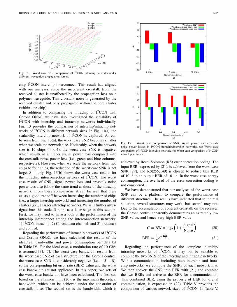
In addition to comparing the intrachip of I2CON withCorona ONoC, we have also investigated the scalability ofI2CON with interchip and intrachip networks individually.Fig. 13 provides the comparison of interchip/intrachip net-works of I2CON in different network sizes. In Fig. 13(a), thescalability interchip network of I2CON is explored. As canbe seen from Fig. 13(a), the worst case SNR becomes smallerwhen we scale the network size. Noticeably, when the networksize is 16 chips (4 × 4), the worst case SNR is negative,which results in a higher signal power loss compared withthe crosstalk noise power loss (i.e., green and blue columns,respectively). However, when we scale the network from twochips to four chips, the reduction of the worst case SNR is notlarge. Similarly, Fig. 13(b) shows the worst case results forthe intrachip interconnection network of I2CON. The worstcase results of SNR, signal power loss, and crosstalk noisepower loss also follow the same trend as those of the intrachipnetwork. From these comparisons, it can be seen that thereexists a good tradeoff between increasing the number of chips(i.e., a larger interchip network) and increasing the number ofclusters (i.e., a larger intrachip network). We will further inves-tigate into this tradeoff point at a later stage in this section.First, we may need to have a look at the performance of theintrachip interconnect among the interconnection networks:1) I2CON intrachip; 2) Corona data channel; and 3) broadcastand control.
Regarding the performance of intrachip networks of I2CONand Corona ONoC, we have calculated the results of theideal/real bandwidths and power consumption per data bitin Table IV. For the ideal case, a modulation rate of 10 Gb/sis assumed [3], [7]. The worst case bandwidth results fromthe worst case SNR of each structure. For the Corona control,the worst case SNR is considerably negative (i.e., −51 dB),so the corresponding bit error rate (BER) value and the worstcase bandwidth are not applicable. In this paper, two sets ofthe worst case bandwidth have been calculated. The first set,based on the Shannon limit (20), is the maximum theoreticalbandwidth, which can be achieved under the constraint ofcrosstalk noise. The second set is the bandwidth, which is
Fig. 13. Worst case comparison of SNR, signal power, and crosstalknoise power losses in I2CON intrachip/interchip networks. (a) Worst casecomparison of I2CON interchip network. (b) Worst case comparison of I2CONintrachip network.
achieved by Reed–Solomon (RS) error correction coding. Theinput BER, expressed by (21), is achieved from the worst caseSNR [29], and RS(255,149) is chosen to reduce this BERof 10−2 to an output BER of 10−12. In the worst case energyconsumption, the overhead of the error correction coding isnot considered.
We have demonstrated that our analyses of the worst caseSNR can be a platform to compare the performance ofdifferent structures. The results have indicated that in the realsituation, several structures may work, but several may not.Due to the accumulation of coherent crosstalk on the receiver,the Corona control apparently demonstrates an extremely lowSNR value, and hence very high BER value
C = BW × log2
(1 + Signal
Noise
)(20)
BER = 1
2e− SNR
4 . (21)
Regarding the performance of the complete interchip/intrachip networks of I2CON, it may not be suitable tocombine the two SNRs of the interchip and intrachip networks.With a communication, including both interchip and intra-chip networks, we compute the SNRs of each network first.We then convert the SNR into BER with (21) and combinethe two BERs and arrive at the BER for a communication.This combined BER, using the property of BER for digitalcommunication, is expressed in (22). Table V provides thecomparison of various network sizes of I2CON. In Table V,

2486 IEEE TRANSACTIONS ON VERY LARGE SCALE INTEGRATION (VLSI) SYSTEMS, VOL. 24, NO. 7, JULY 2016
TABLE IV
IDEAL AND ACTUAL PERFORMANCE: CORONA AND I2CON INTRACHIP
TABLE V
I2CON WORST CASE BER COMPARISON
two different network’s sizes are present: 1) with 256 coresand 2) with 512 cores. With a fixed number of cores, we havevaried the size of intrachip and interchip, and the worst caseBER results are given. As can be seen from Table V, utilizinghigher number of chips rather than using one chip results inbetter worst case BER. For example, regarding the case of256 cores, with only one chip, the worst case BER is 0.03,while the worst case BER is significantly reduced withtwo-chip and four-chip cases. However, when the number ofchips increases, the BER will become worse. For 16-chipinterchip network, we did not have a resulted BER, sincethe SNR of the interchip network is already negative. Similartrend can also be observed with the case of 512-core networks.As a result, we have demonstrated that there is a tradeoff inusing a higher number of chips (instead of higher numberof clusters on chip). Using a single chip is not an optimalsolution, while using so many number of chips may degradethe performance of the network
BERnetwork = BERintra-chip(1 − BERinter-chip)
+ BERinter-chip. (22)
VI. CONCLUSION
In this paper, we have developed the analytical modelsto calculate the signal power loss, the crosstalk noise, andthe SNR in the interchip/intrachip optical networks. In ouranalyses, both the coherent and incoherent crosstalk noisesare analyzed. Utilizing our developed models at the devicelevel, we have provided the analyses of the worst case SNRand crosstalk in both interchip and intrachip levels. I2CONand Corona are chosen as two case studies in order to showthe numerical comparison results. These quantitative results
demonstrate the impact of crosstalk noise on the SNR, theBER, and the network performance. The worst case SNR/BERstrongly depends on the network architecture. More impor-tantly, our analyses of the interchip interconnect have shownthat we could exploit the tradeoffs between the interchip andintrachip interconnects. Our analyses, therefore, can provide aplatform to compare the realistic performance among variousoptical interconnection networks.
REFERENCES
[1] “The international technology roadmap for semiconductors2013 edition,” ITRS, Tech. Rep., 2013.
[2] J. Xu, W. Wolf, J. Henkel, and S. Chakradhar, “A methodology fordesign, modeling, and analysis of networks-on-chip,” in Proc. IEEE Int.Symp. Circuits Syst., vol. 2. May 2005, pp. 1778–1781.
[3] D. Vantrease et al., “Corona: System implications of emerging nanopho-tonic technology,” in Proc. 35th Int. Symp. Comput. Archit., 2008,pp. 153–164.
[4] R. W. Morris, Jr., and A. K. Kodi, “Design of on-chip networksusing microring-resonator based nanophotonic crossbar for future mul-ticores,” in Proc. 23rd Annu. Meeting IEEE Photon. Soc., Nov. 2010,pp. 558–559.
[5] S. Le Beux, J. Trajkovic, I. O’Connor, G. Nicolescu, G. Bois, andP. Paulin, “Optical ring network-on-chip (ORNoC): Architecture anddesign methodology,” in Proc. DATE, Mar. 2011, pp. 1–6.
[6] J. Ahn et al., “Devices and architectures for photonic chip-scale inte-gration,” Appl. Phys. A, vol. 95, no. 4, pp. 989–997, 2009.
[7] X. Wu et al., “An inter/intra-chip optical network for manycore proces-sors,” IEEE Trans. Very Large Scale Integr. (VLSI) Syst., vol. 23, no. 4,pp. 678–691, Apr. 2014.
[8] L. H. K. Duong et al., “A case study of signal-to-noise ratio in ring-basedoptical networks-on-chip,” IEEE Des. Test, vol. 31, no. 5, pp. 55–65,Oct. 2014.
[9] M. Nikdast et al., “Crosstalk noise in WDM-based optical networks-on-chip: A formal study and comparison,” IEEE Trans. Very Large ScaleIntegr. (VLSI) Syst., vol. 23, no. 11, pp. 2552–2565, Nov. 2014.
[10] C.-H. Chen, “Waveguide crossings by use of mutlimode tapered struc-tures,” in Proc. 21st Annu. Wireless Opt. Commun. Conf. (WOCC),Apr. 2012, pp. 130–131.
[11] A. V. Tsarev, “Efficient silicon wire waveguide crossing with negligibleloss and crosstalk,” Opt. Exp., vol. 19, no. 15, pp. 13732–13737,Jul. 2011. [Online]. Available: http://www.opticsexpress.org/abstract.cfm?URI=oe-19-15-13732
[12] F. Xia, L. Sekaric, M. O’Boyle, and Y. Vlasov, “Coupled resonatoroptical waveguides based on silicon-on-insulator photonic wires,” Appl.Phys. Lett., vol. 89, no. 4, pp. 041122-1–041122-3, 2006.
[13] Q. Li, M. Soltani, S. Yegnanarayanan, and A. Adibi, “Design anddemonstration of compact, wide bandwidth coupled-resonator filters ona silicon-on-insulator platform,” Opt. Exp., vol. 17, pp. 2247–2254,Feb. 2009.
[14] S. Xiao, M. H. Khan, H. Shen, and M. Qi, “Modeling and measurementof losses in silicon-on-insulator resonators and bends,” Opt. Exp., vol. 15,no. 17, pp. 10553–10561, 2007.
[15] B. E. Little, S. T. Chu, H. A. Haus, J. Foresi, and J.-P. Laine, “Microringresonator channel dropping filters,” J. Lightw. Technol., vol. 15, no. 6,pp. 998–1005, Jun. 1997.
[16] S. Xiao, M. H. Khan, H. Shen, and M. Qi, “Silicon-on-insulator micror-ing add-drop filters with free spectral ranges over 30 nm,” J. Lightw.Technol., vol. 26, no. 2, pp. 228–236, Jan. 15, 2008.
[17] V. Van, P. P. Absil, J. V. Hryniewicz, and P.-T. Ho, “Propagation lossin single-mode GaAs–AlGaAs microring resonators: Measurement andmodel,” J. Lightw. Technol., vol. 19, no. 11, pp. 1734–1739, Nov. 2001.
[18] Q. Xu, B. Schmidt, J. Shakya, and M. Lipson, “Cascaded silicon micro-ring modulators for WDM optical interconnection,” Opt. Exp., vol. 14,no. 20, pp. 9431–9435, Oct. 2006.
[19] Y. Shen, K. Lu, and W. Gu, “Coherent and incoherent crosstalk inWDM optical networks,” J. Lightw. Technol., vol. 17, no. 5, pp. 759–764,May 1999.
[20] P. Dong et al., “Low loss silicon waveguides for application of opticalinterconnects,” in Proc. IEEE Photon. Soc. Summer Topical MeetingSer., Jul. 2010, pp. 191–192.
[21] F. Xia, L. Sekaric, and Y. Vlasov, “Ultracompact optical buffers on asilicon chip,” Nature Photon., vol. 1, no. 1, pp. 65–71, 2007.
[22] J. Chan, G. Hendry, K. Bergman, and L. P. Carloni, “Physical-layermodeling and system-level design of chip-scale photonic interconnectionnetworks,” IEEE Trans. Comput.-Aided Design Integr. Circuits Syst.,vol. 30, no. 10, pp. 1507–1520, Oct. 2011.

DUONG et al.: COHERENT AND INCOHERENT CROSSTALK NOISE ANALYSES 2487
[23] A. Joshi et al., “Silicon-photonic clos networks for global on-chip com-munication,” in Proc. 3rd ACM/IEEE Int. Symp. Netw.-Chip, May 2009,pp. 124–133.
[24] Q. Xu, B. Schmidt, S. Pradhan, and M. Lipson, “Micrometre-scale sili-con electro-optic modulator,” Nature, vol. 435, pp. 325–327, May 2005.
[25] G. Masini, G. Capellini, J. Witzens, and C. Gunn, “A 1550 nm,10 Gbps monolithic optical receiver in 130 nm CMOS with integratedGe waveguide photodetector,” in Proc. 4th IEEE Int. Conf. Group IVPhoton., Sep. 2007, pp. 1–3.
[26] I. M. Soganci, A. La Porta, and B. J. Offrein, “Flip-chip opticalcouplers with scalable I/O count for silicon photonics,” Opt. Exp.,vol. 21, no. 13, pp. 16075–16085, Jul. 2013. [Online]. Available:http://www.opticsexpress.org/abstract.cfm?URI=oe-21-13-16075
[27] Y. Pan, J. Kim, and G. Memik, “FlexiShare: Channel sharing for anenergy-efficient nanophotonic crossbar,” in Proc. IEEE 16th Int. Symp.High Perform. Comput. Archit., Jan. 2010, pp. 1–12.
[28] P. Koka, M. O. McCracken, H. Schwetman, X. Zheng, R. Ho, andA. V. Krishnamoorthy, “Silicon-photonic network architectures for scal-able, power-efficient multi-chip systems,” in Proc. 37th Annu. Int. Symp.Comput. Archit., New York, NY, USA, 2010, pp. 117–128.
[29] Y. Xie et al., “Crosstalk noise and bit error rate analysis for opti-cal network-on-chip,” in Proc. 47th ACM/IEEE Design Autom. Conf.,Jun. 2010, pp. 657–660.
Luan H. K. Duong (S’14) received the B.S. degreein computer science from The Hong Kong Universityof Science and Technology, Hong Kong, in 2012,where he is currently pursuing the Ph.D. degree inelectronic and computer engineering.
His current research interests include embeddedsystem, system-on-chip, and optical interconnectionnetworks.
Zhehui Wang (S’11) received the B.S. degree in electrical engineering fromFudan University, Shanghai, China, in 2010. He is currently pursuing thePh.D. degree with the Department of Electronic and Computer Engineering,The Hong Kong University of Science and Technology, Hong Kong.
His current research interests include embedded system, multiprocessorsystems, network-on-chip, and floorplan design for network-on-chip.
Mahdi Nikdast (S’10–M’14) received the Ph.D. degree in electronic andcomputer engineering from The Hong Kong University of Science andTechnology, Hong Kong, in 2014.
He is currently a Post-Doctoral Fellow with the Computer and SoftwareEngineering Department, École Polytechnique de Montréal, Montréal, QC,Canada. His current research interests include embedded and computingsystems, networks-on-chip, and optical interconnection networks.
Jiang Xu (S’02–M’07) received the Ph.D. degreefrom Princeton University, Princeton, NJ, USA,in 2007.
He was a Research Associate with Bell Labora-tories, Murray Hill, NJ, USA, from 2001 to 2002,and with NEC Laboratories America, Inc.,Princeton, NJ, USA, from 2003 to 2005. He joineda startup company, Sandbridge Technologies, Inc.,Tarrytown, NY, USA, from 2005 to 2007, andhe developed and implemented two generationsof network-on-chip (NoC)-based ultralow-power
multiprocessor systems-on-chip (SoCs) for mobile platforms. He is currentlyan Associate Professor with The Hong Kong University of Science andTechnology (HKUST), Hong Kong. He is the Founding Director ofXilinx–HKUST Joint Laboratory and established Mobile Computing SystemLaboratory and Optical/Photonic Technology for Interconnected ComputingSystem Laboratory. He has authored or co-authored more than 90 bookchapters and papers in peer-reviewed journals and international conferences.His current research interests include NoC, multiprocessor SoC, opticalinterconnects, embedded system, computer architecture, low-power VLSIdesign, and hardware/software codesign.
Dr. Xu currently serves as the Area Editor of NoC, SoC, and GPU for ACMTransactions on Embedded Computing Systems and an Associate Editor of theIEEE TRANSACTIONS ON VERY LARGE SCALE INTEGRATION SYSTEMS.He is the IEEE Distinguished Lecturer and was an ACM DistinguishedSpeaker. He served on the steering committees, organizing committees, andtechnical program committees of many international conferences.
Peng Yang received the B.S. degree in electronic science and technologyfrom Wuhan University, Wuhan, China, in 2013. He is currently pursuing thePh.D. degree in electronic and computer engineering with The Hong KongUniversity of Science and Technology, Hong Kong.
His current research interests include optical networks-on-chip, system-on-chip, and embedded system.
Zhifei Wang received the B.Eng. degree in information engineering from Zhe-jiang University, Hangzhou, China. He is currently pursuing the Ph.D. degreein electronic and computer engineering with The Hong Kong University ofScience and Technology, Hong Kong.
His current research interests include optical networks-on-chip, system-on-chip, and embedded system.
Zhe Wang (S’14) received the B.S. degree in electronic engineering fromShanghai Jiao Tong University, Shanghai, China, in 2011. He is currentlypursuing the Ph.D. degree in electronic and computer engineering with TheHong Kong University of Science and Technology, Hong Kong.
His current research interests include hardware/software codesign, anddesign space exploration techniques.
Rafael K. V. Maeda received the B.S. degree in electrical engineeringfrom the Federal University of Minas Gerais, Belo Horizonte, Brazil, in 2013.He is currently pursuing the Ph.D. degree in electronic and computerengineering with The Hong Kong University of Science and Technology,Hong Kong.
His current research interests include computer architecture, heterogeneouscomputing, and multiprocessor systems-on-chip.
Haoran Li received the B.E. degree in electronic and information engineeringfrom Zhejiang University, Hangzhou, China, in 2014. He is currently pursuingthe Ph.D. degree in electronic and computer engineering with The Hong KongUniversity of Science and Technology, Hong Kong.
His current research interests include embedded system, networks-on-chip,and computer architecture.
Xuan Wang (S’12) received the B.S. degree in electrical engineering fromShanghai Jiao Tong University, Shanghai, China, in 2009. He is currentlypursuing the Ph.D. degree with the Department of Electronic and ComputerEngineering, The Hong Kong University of Science and Technology,Hong Kong.
His current research interests include embedded system, network-on-chip,and fault tolerant design and reliability issues in very deep submicrometertechnologies.
Sébastien Le Beux (S’09) received the Ph.D. degree from the University ofLille, Villeneuve-d’Ascq, France, in 2007.
He has been an Associate Professor with the École Centrale de Lyon,Écully, France, since 2010. His current research interests include designmethods for emerging (nano)technologies and embedded systems.
Yvain Thonnart received the M.S. degree from the École Polytechnique,Palaiseau, France, in 2003, and the Engineering Diploma degree from Tele-cosm ParisTech, Paris, France, in 2005.
He joined the CEA-LETI Laboratory, Grenoble, France. His currentresearch interests include low-power design and networks-on-chip.