ieee transactions on very large scale integration (vlsi ...sudeep/wp-content/uploads/j32.pdf ·...
TRANSCRIPT
IEEE TRANSACTIONS ON VERY LARGE SCALE INTEGRATION (VLSI) SYSTEMS, VOL. 24, NO. 1, JANUARY 2016 3
A System-Level Cosynthesis Framework for PowerDelivery and On-Chip Data Networks in
Application-Specific 3-D ICsNishit Kapadia, Student Member, IEEE, and Sudeep Pasricha, Senior Member, IEEE
Abstract— With increasing core counts ushering in power-constrained 3-D multiprocessor system-on-chips (MPSoCs),optimizing communication power dissipated by the3-D network-on-chip (NoC) fabric is critical. At the sametime, with increased power densities in 3-D ICs, problemsof IR drops in the power delivery network (PDN) as well asthermal hot spots on the 3-D die are becoming very severe. Eventhough the PDN and NoC design goals are nonoverlapping, boththe optimizations are interdependent. Unfortunately, designerstoday seldom consider the design of the PDN, while designingNoCs. Moreover, for each new configuration of computation coreand communication mapping on an MPSoC, the correspondingintercore communication patterns, 3-D on-chip thermal profile,as well as IR-drop distribution in the PDN can vary significantly.Based on this observation, we propose a novel design-timesystem-level application-specific cosynthesis framework thatintelligently maps computation and communication resourceson a die, for a given workload. The goal is to minimize theNoC power as well as chip-cooling power and optimize the3-D PDN architecture; while meeting performance goals andsatisfying thermal constraints, for a microfluidic cooling-basedapplication-specific 3-D MPSoC. Our experimental resultsindicate that the proposed 3-D NoC-PDN cosynthesis frameworkis not only able to meet PDN design goals unlike prior 3-D NoCsynthesis approaches, but also provides better overall optimalitywith the solution quality improvement of up to 35.4% overa probabilistic metaheuristic-based cooptimization approachproposed in prior work.
Index Terms— 3-D ICs, multicore systems, network-on-chip (NoC) synthesis, power delivery networks (PDNs),system-level CAD.
I. INTRODUCTION
DESIGNING a robust power delivery network (PDN) iscritical to the overall performance of today’s multiproces-
sor system-on-chips (MPSoCs). The PDN is required to delivera stable power supply across the chip that is within a desiredvoltage range and tolerate large variations in load currents [1].For the case of multiple voltage islands (VIs) that are usedin modern MPSoC designs to minimize power dissipation,
Manuscript received March 27, 2014; revised August 14, 2014 andDecember 16, 2014; accepted January 29, 2015. Date of publicationFebruary 26, 2015; date of current version December 24, 2015. This workwas supported in part by the National Science Foundation under Grant CCF-1252500 and Grant CCF-1302693 and in part by the Semiconductor ResearchCorporation.
The authors are with the Department of Electrical and ComputerEngineering, Colorado State University, Fort Collins, CO 80523 USA (e-mail:[email protected]; [email protected]).
Color versions of one or more of the figures in this paper are availableonline at http://ieeexplore.ieee.org.
Digital Object Identifier 10.1109/TVLSI.2015.2399279
the PDN is required to supply power at different voltagelevels corresponding to the VIs, while keeping power lossto a minimum. Unfortunately, with increasing on-chip devicedensity and decreasing voltage levels, the supply currents haverisen; however, the scaling of PDN impedance has not kept upwith this trend [2]. The resulting worsening of IR drops in thePDN has led to a reduction in the quality of voltage supplyand negatively impacted MPSoC performance, because circuitdelay in modern technologies has been shown to have a strongnonlinear relationship to the supply voltage drop [3]. Thisproblem is even more severe in 3-D MPSoCs as the current inthe PDN can be as many times more as the number of devicelayers compared with a 2-D MPSoC. Moreover, the numberof I/O pins on an n-layered 3-D design is about n times smallerthan its 2-D counterpart, thus exacerbating the problem of adegraded voltage supply in 3-D designs [4].
The design of 3-D MPSoCs faces another well-documentedchallenge: that of achieving an acceptable thermal profileacross the 3-D die. Due to increased power densities andthermal resistivity in 3-D chips, conventional air-cooled heatsinks may be insufficient to remove heat dissipated inhigh-performance 3-D chips [37]. Microfluidic cooling hasrecently been proposed as an attractive alternative due tothe superior heat removal capability of liquids in comparisonwith air [5], [6]. However, cooptimizing cooling and PDNcosts remain a challenging and unaddressed problem for3-D MPSoCs.
Another critical component at the heart of emerging3-D MPSoCs is the network-on-chip (NoC) architecture thatenables intralayer and interlayer communication betweenmultiple cores. As the power dissipated in the NoC has becomea significant portion of the total on-chip power, optimizingcommunication power has become a critical step in today’schip design methodologies. Prior works on NoC synthesis donot consider the design of the PDN, while mapping coresand designing the NoC fabric, and typically generate a singlepower and performance optimized NoC configuration that mayor may not meet thermal constraints. Performing synthesisof the PDN for the generated NoC configuration in thesecases can put stringent demands on the already strained PDN,making it extremely difficult to meet PDN constraints suchas max-IR-drop or leading to overmargining for the PDN(e.g., requiring large grid-wire width) that can be wasteful andprohibitively increase overall system cost.
We recognize the key insight that different instances ofvoltage partitioning and core-to-tile mapping can significantly
1063-8210 © 2015 IEEE. Personal use is permitted, but republication/redistribution requires IEEE permission.See http://www.ieee.org/publications_standards/publications/rights/index.html for more information.
4 IEEE TRANSACTIONS ON VERY LARGE SCALE INTEGRATION (VLSI) SYSTEMS, VOL. 24, NO. 1, JANUARY 2016
alter the IR-drop distribution map observed by the PDN aswell as the thermal profile of the 3-D chip. Therefore, ourframework integrates efficient mechanisms for VI-aware coremapping on the 3-D die and exploits the interdependencebetween the synthesized 3-D NoC configuration, the resultingthermal profile of the 3-D chip, and its corresponding IR-dropdistribution across the 3-D PDN. The novel contribu-tions of our cosynthesis framework are summarized asfollows.
1) We integrate models of the PDN, microfluidic cooling,VIs, and 3-D NoCs into a system-level optimizationframework.
2) We propose a design time force-directed algorithm tomap cores onto the tiles of a 3-D die, while cooptimizingcommunication, thermal, and PDN design objectives togenerate an optimized application-specific 3-D MPSoC.
3) We also propose a simulated-annealing (SA)-basedcosynthesis approach to optimize communication,thermal, and PDN goals.
4) We design an algorithm for 3-D routing path allocationthat considerably minimizes power in the 3-D NoC.
5) Our framework ultimately generates a set of designpoints (Pareto mappings) that allow a designer totradeoff the quality of the PDN against NoC power costsand cooling power costs, and select a suitable solutionthat meets power, performance, and PDN cost-baseddesign goals.
II. RELATED WORK
The problem of 2-D NoC synthesis on regular structureswith multiple supply VIs has been addressed in [18] and [25].Jang et al. [25] limit power overhead by reducing the totalnumber of voltage level converters (VLCs) and multiple-clockfirst-in first-out (MCFIFO) frequency level converters neededfor interisland transfers. Our prior work [18] improvesupon [25] with heuristics that generate a better core-to-tilemapping, and a routing scheme that more aggressivelyoptimizes interisland communication.
Given the promise of 3-D technologies, 3-D NoCsynthesis in recent years has also attracted significant researchefforts [7], [27], [31]. Seiculescu et al. [27] perform min-cutpartitioning of cores to establish core-to-router connectivityin 3-D ICs, find paths for the communication flows, andplace network components on the 3-D layers; while reportingsavings in NoC power consumption and delay. In [31],improvements are shown over [27] by additionally consideringthe impact of through silicon via (TSV) serialization andnetwork interface placement in irregular 3-D NoCs. Recently,Matsutani et al. [7] have proposed a novel 3-D NoC topologyemploying randomized long links at one or more dies of the3-D stack, thereby significantly reducing the average hopcount, communication latency, and communication energycompared with a regular 3-D mesh topology. However, noneof these existing approaches have considered the impactof 3-D NoC synthesis on the efficiency and overheadsassociated with 3-D PDN design; in other words, theseapproaches are not PDN aware. These prior efforts also do notconsider optimization for microfluidic cooling-based 3-D ICs.
On the other hand, techniques for optimizing PDNsin 3-D ICs have been studied in [1], [2], [4], [11], and [12].In [4], the impact of TSV size/spacing on IR drops and voltagedroops in several 3-D PDN configurations is analyzed, forSPEC benchmarks running on a quad-core SoC. In [11], SAis used to cosynthesize the floorplan and power-ground (P/G)network, optimizing wire length, area, P/G routing area, andIR drops. In [12], an integrated 3-D TSV, thermal, and powerdistributed network (STDN) is proposed; and an SA floorplan-ner is used to minimize the voltage drop and temperature inSTDN. None of these PDN optimization techniques considersthe impact of the 3-D NoC fabric and core mapping acrosslayers, or considers 3-D chips with microfluidic cooling asan optimization platform. Kapadia and Pasricha [32] motivatethe need for a PDN-NoC cosynthesis methodology, and pro-poses an SA-based cosynthesis framework for 3-D MPSoCs,which is shown to generate more efficient overall solutionscompared with a PDN-unaware synthesis approach. However,the proposed approach fails to consider the thermal costs andcooling costs associated with the generated solutions.
Unlike any prior work, in this paper, we present anovel thermal-aware cosynthesis framework for core mapping,PDN design, and mesh-based NoC design in 3-D MPSoCs.To the best of our knowledge, this is the first work thatproposes a system-level cosynthesis framework to cooptimizea 3-D NoC fabric, 3-D chip thermal profile, and 3-D PDNfabric to produce a more efficient overall MPSoC design.This paper significantly extends our recent conferencepublication [32] with new heuristics and the integrationof thermal and cooling awareness during the optimizationflow. Our experimental studies present detailed comparisonsbetween our new framework in this paper and the approachfrom [32].
III. PDN DESIGN FOR 3-D MPSoC
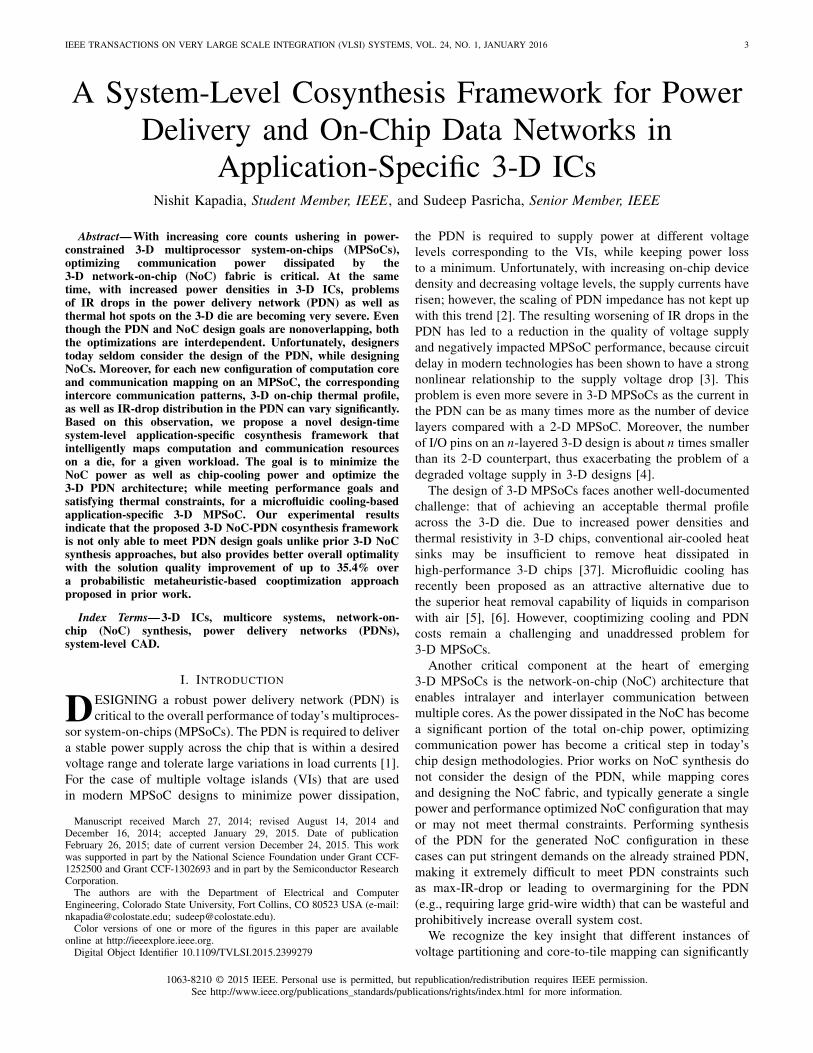
High circuit density in small footprint 3-D ICs presents aunique challenge for designers of PDNs, as it requires thenetwork to deliver significantly more current than in2-D ICs with fewer P/G bumps, while overcoming increasinglydaunting IR-drop issues. As circuit delay is strongly corelatedto the supply voltage drop in modern technologies, the PDNshould at least be able to restrict IR drops at each core-inputwithin the set tolerance limit, usually 5%–10% of the ratedcore voltage [3]. In this paper, we consider an MPSoCplatform with a 3-D mesh of tiles, with multiple voltagedomains (i.e., VIs), where there is a one-to-one mapping ofprocessing cores onto these tiles. The voltage assignmentsof cores running a multiprogrammed workload represent theoperating frequency requirements of the tasks mapped onthem, and the supply-current assignments of cores representthe power requirements for running the mapped tasks. In orderfor the PDN to handle multiple voltage domains, we assumethat the MPSoC design is partitioned into 3-D-VIs such thatcores of the same voltage are vertically aligned in the 3-Dstack (as shown in Fig. 1), similar to the voltage volumeconcept introduced in [12] (although, we consider multipleVI configurations using all possible 2-D-shapes of VIs in our
KAPADIA AND PASRICHA: SYSTEM-LEVEL COSYNTHESIS FRAMEWORK FOR PDN AND ON-CHIP DATA NETWORKS 5
Fig. 1. Example of contiguous 3-D VIs in a 27 core (3 × 3 × 3)3-D MPSoC. Cores within a single 3-D-VI are vertically aligned (VIs arecolor-coded). Only the 3-D power grid for the blue VI is shown for clarity.Each VI has a separate power grid, with 16 grid nodes per core.
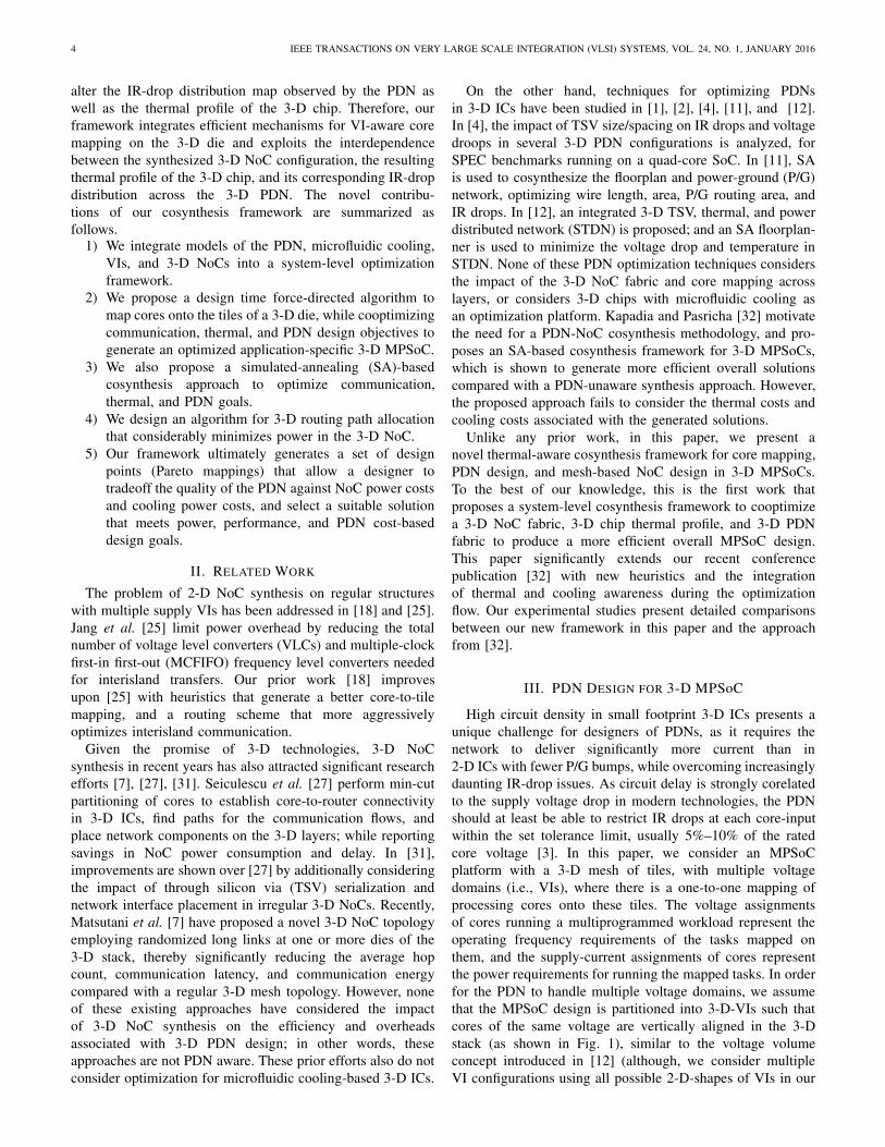
Fig. 2. Interlayer liquid cooling [5]. (a) Cross section of a 3-D chip.(b) Top-view of microchannels (blue area) with fluid flowing from left to right.
synthesis approach). This enables independent and physicallydisjoint 3-D power supply grids to connect all cores operatingat the same voltage. The points of intersection in any3-D power grid are termed as grid nodes, which supply powerto the cores (16 grid nodes are assumed per core, as shownin Fig. 1). The interlayer connections in the grid are madeusing power TSVs. Even though all VIs are contiguous, wedo not restrict the VI shapes to rectangles (as assumed inprior works, such as [33]). It is shown in [34] that sizingof pitches and widths of the power grid does not changethe on-chip voltage distribution; therefore, in this paper, weassume fixed uniform power grids, as in [34] and [35], i.e.,the grid nodes and the corresponding power-TSVs/power-pinsare located uniformly over each core (as shown in Fig. 1).Note, this paper considers the steady-state characterization ofthe thermal, PDN, communication, and computation profilesof MPSoCs. Therefore, we investigate the steady-state effectsof the global power grid in terms of static IR drop, whiletime-varying network characteristics, such as transient noise,are not considered.
IV. INTERTIER LIQUID COOLING IN 3-D ICs
The structure of the microfluidic layers with microchannelsfor fluid delivery and with the possible locations of intertierTSVs is shown in Fig. 2(b). Given the effectiveness
of microfluidic cooling, we do not need thermal TSVsin 3-D ICs, as also assumed in the other works on microfluidiccooling [5], [6], [39]. In this paper, we use a microfluidic layerunder each device layer as suggested in [5]. Note that as themicrofluid within microchannels progresses from the fluid inlettoward the fluid outlet [Fig. 2(a)], its capacity to absorb heatflux from device layers steadily decreases [39] from the inletto the outlet. By increasing fluid flow rates, it is possible forthe fluid to absorb more heat flux from the cores closer to theoutlet, helping to reduce their temperatures.
In this paper, we assume that the hot water exiting the3-D chip is cooled (to a fixed ambient temperature) by aheat sink with a radiator-fan assembly and fed back intothe fluid inlets of the chip (as in [28]–[30]). Higher fluidflow rates require the fan-based heat sink to accommodatehigher heat transfer rates (as discussed in Section VI-E),with higher number of rotations per minute (r/min).Higher r/min values in turn increase the fan power (Pfan), infact, Pfan ∝ (r/min)3 [28]. In addition, the electrical powerrequired to pump the fluid into the 3-D-chip is directlyproportional to the square of the flow rate (Ppump ∝ Fl2) [5].Therefore, even though serious thermal problems can generallybe alleviated by increasing fluid flow rates, indiscriminatelyramping up flow rates in practice can potentially lead toprohibitively high cooling power (Pfan + Ppump), and thusviolate chip power budgets. Consequently, the design of amicrofluidic cooled 3-D MPSoC requires careful planningduring the allocation of computational and network resourceson the die.
V. PROBLEM FORMULATION
In this section, we present our problem formulation.We assume the following inputs to our problem.
1) A 3-D IC with a regular 3-D mesh NoC, with dimensions(dimx, dimy , and dimz) and number of tilesT = dimx × dimy × dimz with each tile containing acore and a NoC router.
2) A core graph G(V , E) with a set of T vertices{V1, V2, . . . , VT } representing homogenous computecores on which application tasks have already beenmapped, and the set of M edges {e1, e2, . . . , eM } thatrepresent communication flow dependence andrequirements between cores.
3) A minimum communication bandwidth constraint foreach communication flow; and latency constraints rep-resented as an upper bound on number of hops{h1, h2, . . . , hM } for each communication flow.
4) A set of preassigned triplets constituting operatingvoltages, operating frequencies, and maximum supplycurrents for the T cores {(v1, f1, i1), (v2, f2, i2),(v3, f3, i3), . . . , (vT , fT , iT )} in the core graph, to meetcompute performance and power requirements of tasksmapped to the cores.
5) A set of � supply voltage (vdd) levels, which alsorepresents the total number of VIs.
6) � separate regular 3-D power grids (each correspondingto a VI), with multiple power input pins for every grid.
6 IEEE TRANSACTIONS ON VERY LARGE SCALE INTEGRATION (VLSI) SYSTEMS, VOL. 24, NO. 1, JANUARY 2016
7) A maximum temperature constraint � for the entirechip, and a max-IR-drop constraint � for the PDN.
Based on the minimum voltage/frequency requirements ofthe T cores (which in turn depends on the performancedemands of tasks assigned on each core), we assume thatvoltage partitioning (assignment of available {voltage andfrequency} pairs to the T cores) has already been per-formed using techniques from [18] and [25]. Note that asthe (vx , fx , ix) triplets for each core are fixed, total compu-tation power in our cosynthesis framework is predetermined.However, the manner in which compute and communicationresources are mapped on the die can alter communicationpower, cooling power, and 3-D PDN design costs.
Objective: Given the above inputs, the goal of our proposedframework is to obtain a core-to-die mapping and synthesize aregular 3-D mesh NoC for a specific application, such that theapplication performance constraints (bandwidth and latencyconstraints), 3-D-VI contiguity constraints (all cores arecontiguously placed within individual 3-D VIs), and themaximum chip temperature constraint are satisfied, whileminimizing total communication power and cooling power,as well as PDN cost (represented by the max-IR-drop).Note that our proposed framework is also applicable to 2-DMPSoCs [with the vertical NoC dimension (dimz) set to 1].
VI. COSYNTHESIS FRAMEWORK OVERVIEW
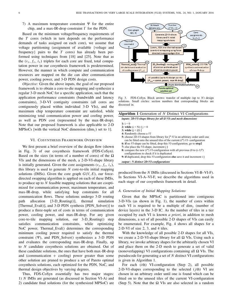
We first present a brief overview of the design flow (shownin Fig. 3) of our cosynthesis framework (FDS-CoSyn).Based on the sizes (in terms of a number of cores) of the �VIs and the dimensions of the mesh, a 2-D-VI-shape libraryis initially generated. Given the core assignments (vx , fx , ix),this library is used to generate N core-to-tile initial mappingsolutions (IMSs). Given the core graph G(V, E), our force-directed swapping algorithm is applied on each of these IMSs,to produce up to N feasible mapping solutions that are coopti-mized for communication power, maximum temperature, andmax-IR-drop, while satisfying hop constraints for allcommunication flows. These solutions undergo 3-D routingpath allocation [3-D_Routing()], thermal simulation[Thermal_Eval()], and 3-D PDN synthesis [PDN_Solver()] toproduce a three-tuple set of costs in terms of communicationpower, cooling power, and max-IR-drop. For any givencore-to-tile mapping solution, our 3-D_Routing() stepsatisfies communication constraints, while optimizingNoC power, Thermal_Eval() determines the correspondingminimum cooling power required to satisfy the thermalconstraint (�), and PDN_Solver() synthesizes a 3-D PDNand evaluates the corresponding max-IR-drop. Finally, upto N candidate cosynthesis solutions are obtained. Out ofthese candidate solutions, the ones that have both max-IR-dropand (communication + cooling) power greater than someother solution are pruned to produce a set of Pareto optimalcosynthesis solutions, each optimized for the PDN, NoC, andthermal design objectives by varying degrees.
Thus, FDS-CoSyn essentially has two major stages:1) N IMSs are generated (as discussed in Section VI-A) and2) candidate final solutions (for the synthesized MPSoC) are
Fig. 3. FDS-CoSyn. Block arrows: transfer of multiple (up to N ) designsolutions. Small circles: section numbers that corresponding blocks arediscussed in.
Algorithm 1 Generation of N Distinct VI Configurations
produced from the N IMSs (discussed in Sections VI-B–VI-F).In Sections VI-A–VI-F, we describe the algorithms used ineach stage of our cosynthesis framework in detail.
A. Generation of Initial Mapping Solutions
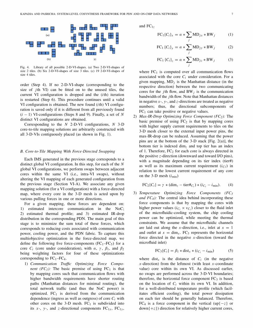
Given that the MPSoC is partitioned into contiguous3-D-VIs (as shown in Fig. 1), the number of cores withineach VI is required to be a multiple of dimz (number ofdevice layers) in the 3-D IC. As the number of tiles in a tieroccupied by each VI is known a priori, in addition to meshdimensions, a set of all possible 2-D shapes of VIs can easilybe enumerated. For example, Fig. 4 shows all shapes for a2-D-VI of size 2, 3, and 4 tiles.
With the knowledge of all possible 2-D shapes for all VIs,we create a 2-D-VI-shape library for all � VIs. Using such alibrary, we invoke arbitrary shapes for the arbitrarily chosen VIand place them on the 2-D mesh to generate a set of valid(nonoverlapping) VI configurations containing all � VIs. Thepseudocode for generating a set of N distinct VI configurationsis given in Algorithm 1.
For each (i th) VI-configuration (Step 2), all possible2-D-VI-shapes corresponding to the selected ( j th) VI arechosen in an arbitrary order until one is found which can befitted on to the unused tiles of the current VI-configuration(Step 5). Note that the � VIs are also selected in a random
KAPADIA AND PASRICHA: SYSTEM-LEVEL COSYNTHESIS FRAMEWORK FOR PDN AND ON-CHIP DATA NETWORKS 7
Fig. 4. Library of all possible 2-D-VI-shapes. (a) Two 2-D-VI-shapes ofsize 2 tiles. (b) Six 2-D-VI-shapes of size 3 tiles. (c) 19 2-D-VI-shapes ofsize 4 tiles.
order (Step 4). If no 2-D-VI-shape (corresponding to thesize of j th VI) can be fitted on to the unused tiles, thecurrent VI configuration is dropped and the (i th) iterationis restarted (Step 6). This procedure continues until a validVI configuration is obtained. The new found (i th) VI configu-ration is saved only if it is different from all previously found(i − 1) VI-configurations (Steps 8 and 9). Finally, a set of Ndistinct VI configurations are obtained.
Corresponding to the N 2-D-VI configurations, N 3-Dcore-to-tile mapping solutions are arbitrarily constructed withall 3-D-VIs contiguously placed (as shown in Fig. 1).
B. Core-to-Tile Mapping With Force-Directed Swapping
Each IMS generated in the previous stage corresponds to adistinct global VI configuration. In this step, for each of the Nglobal VI configurations, we perform swaps between adjacentcores within the same VI (i.e., intra-VI swaps), withoutaltering the VI mapping of each generated configuration fromthe previous stage (Section VI-A). We associate any givenmapping solution (for a VI configuration) with a force-directedmap, where every core in the 3-D mesh is acted upon byvarious pulling forces in one or more directions.
For a given mapping, these forces are dependent on:1) estimated intercore communication in the NoC;2) estimated thermal profile; and 3) estimated IR-dropdistribution in the corresponding PDN. The main goal of thisstage is to minimize the sum total of these forces, whichcorresponds to reducing costs associated with communicationpower, cooling power, and the PDN fabric. To capture thismultiobjective optimization in the force-directed map, wedefine the following five force-components (FC1–FC5) for acore Ci (core under consideration), with α, γ , β1, and β2being weighting factors for four of these optimizationscorresponding to FC1–FC4.
1) Communication Traffic Optimizing Force Compo-nent (FC1): The basic premise of using FC1 is thatby mapping cores such that communication flows withhigher bandwidth requirements have shorter routingpaths (Manhattan distances for minimal routing), thetotal network traffic (and thus the NoC power) isoptimized. FC1 is derived from the communicationdependence (ingress as well as outgress) of core Ci withother cores on the 3-D mesh. FC1 is subdivided intoits x-, y-, and z-directional components FC1x , FC1y ,
and FC1z
FC1{Ci }x = α ∗∑
j
MD j x ∗ BW j (1)
FC1 {Ci }y = α ∗∑
j
MD j y ∗ BW j (2)
FC1 {Ci }z = α ∗∑
j
MD j z ∗ BW j (3)
where FC1 is computed over all communication flowsassociated with the core Ci under consideration. For agiven mapping, MD j is the Manhattan distance (in therespective direction) between the two communicatingcores for the j th flow, and BW j is the communicationbandwidth of the j th flow. Note that Manhattan distancesin negative x-, y-, and z-directions are treated as negativenumbers; thus, the directional subcomponents ofFC1 can take positive or negative values.
2) Max-IR-Drop Optimizing Force Component (FC2): Thebasic premise of using FC2 is that by mapping coreswith higher supply current requirements to tiles on the3-D mesh closer to the external input power pins, themax-IR-drop can be reduced. Assuming that the powerpins are at the bottom of the 3-D stack [Fig. 2(a)], thebottom tier is indexed dimz and top tier has an indexof 1. Therefore, FC2 for each core is always directed inthe positive z-direction (downward and toward I/O pins),with a magnitude depending on its tier index (tier#)as well as its maximum current requirement (iCi) inrelation to the lowest current requirement of any coreon the 3-D mesh (imin)
FC2{Ci } = γ ∗ (dimz − tier#Ci ) ∗ (iCi − imin). (4)
3) Temperature Optimizing Force Components (FC3
and FC4): The central idea behind incorporating theseforce components is that by mapping the cores withhigher power values (iCi × vCi ) closer to the fluid inletof the microfluidic-cooling system, the chip coolingpower can be optimized, while meeting the thermalconstraints. We assume that the microfluidic channelsare laid out along the x-direction, i.e., inlet at x = 1and outlet at x = dimx . FC3 represents the horizontalforce directed in the negative x-direction (toward themicrofluid inlet)
FC3{Ci } = β1 ∗ distx ∗ (iCi − imin) (5)
where distx is the distance of Ci (in the negativex-direction) from the leftmost (with least x-coordinatevalue) core within its own VI. As discussed earlier,no swaps are performed across the 3-D-VI boundaries;therefore, the horizontal force component FC3 is basedon the location of Ci within its own VI. In addition,for a well-distributed temperature profile (which facil-itates efficient cooling), the total power dissipationon each tier should be generally balanced. Therefore,FC4 is a force component in the vertical (up{−z} ordown{+z}) direction for relatively higher current cores,
8 IEEE TRANSACTIONS ON VERY LARGE SCALE INTEGRATION (VLSI) SYSTEMS, VOL. 24, NO. 1, JANUARY 2016
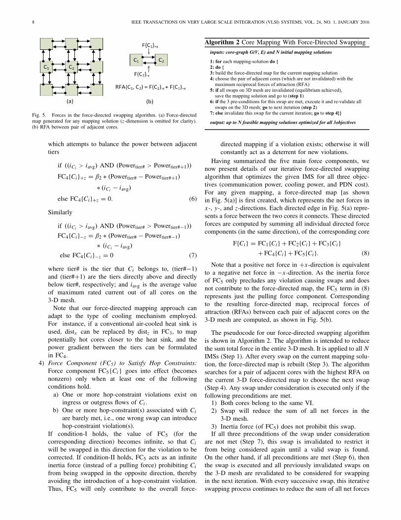
Fig. 5. Forces in the force-directed swapping algorithm. (a) Force-directedmap generated for any mapping solution (z-dimension is omitted for clarity).(b) RFA between pair of adjacent cores.
which attempts to balance the power between adjacenttiers
if ((iCi > iavg) AND (Powertier# > Powertier#+1))
FC4{Ci }+z = β2 ∗ (Powertier# − Powertier#+1)
∗ (iCi − iavg)
else FC4{Ci }+z = 0. (6)
Similarly
if ((iCi > iavg) AND (Powertier# > Powertier#−1))
FC4{Ci }−z = β2 ∗ (Powertier# − Powertier#−1)
∗ (iCi − iavg)
else FC4{Ci }−z = 0 (7)
where tier# is the tier that Ci belongs to, (tier#−1)and (tier#+1) are the tiers directly above and directlybelow tier#, respectively; and iavg is the average valueof maximum rated current out of all cores on the3-D mesh.
Note that our force-directed mapping approach canadapt to the type of cooling mechanism employed.For instance, if a conventional air-cooled heat sink isused, distx can be replaced by distz in FC3, to mappotentially hot cores closer to the heat sink, and thepower gradient between the tiers can be formulatedin FC4.
4) Force Component (FC5) to Satisfy Hop Constraints:Force component FC5{Ci } goes into effect (becomesnonzero) only when at least one of the followingconditions hold.
a) One or more hop-constraint violations exist oningress or outgress flows of Ci .
b) One or more hop-constraint(s) associated with Ci
are barely met, i.e., one wrong swap can introducehop-constraint violation(s).
If condition-I holds, the value of FC5 (for thecorresponding direction) becomes infinite, so that Ci
will be swapped in this direction for the violation to becorrected. If condition-II holds, FC5 acts as an infiniteinertia force (instead of a pulling force) prohibiting Ci
from being swapped in the opposite direction, therebyavoiding the introduction of a hop-constraint violation.Thus, FC5 will only contribute to the overall force-
Algorithm 2 Core Mapping With Force-Directed Swapping
directed mapping if a violation exists; otherwise it willconstantly act as a deterrent for new violations.
Having summarized the five main force components, wenow present details of our iterative force-directed swappingalgorithm that optimizes the given IMS for all three objec-tives (communication power, cooling power, and PDN cost).For any given mapping, a force-directed map [as shownin Fig. 5(a)] is first created, which represents the net forces inx-, y-, and z-directions. Each directed edge in Fig. 5(a) repre-sents a force between the two cores it connects. These directedforces are computed by summing all individual directed forcecomponents (in the same direction), of the corresponding core
F{Ci } = FC1{Ci } + FC2{Ci } + FC3{Ci }+ FC4{Ci } + FC5{Ci }. (8)
Note that a positive net force in +x-direction is equivalentto a negative net force in −x-direction. As the inertia forceof FC5 only precludes any violation causing swaps and doesnot contribute to the force-directed map, the FC5 term in (8)represents just the pulling force component. Correspondingto the resulting force-directed map, reciprocal forces ofattraction (RFAs) between each pair of adjacent cores on the3-D mesh are computed, as shown in Fig. 5(b).
The pseudocode for our force-directed swapping algorithmis shown in Algorithm 2. The algorithm is intended to reducethe sum total force in the entire 3-D mesh. It is applied to all NIMSs (Step 1). After every swap on the current mapping solu-tion, the force-directed map is rebuilt (Step 3). The algorithmsearches for a pair of adjacent cores with the highest RFA onthe current 3-D force-directed map to choose the next swap(Step 4). Any swap under consideration is executed only if thefollowing preconditions are met.
1) Both cores belong to the same VI.2) Swap will reduce the sum of all net forces in the
3-D mesh.3) Inertia force (of FC5) does not prohibit this swap.If all three preconditions of the swap under consideration
are not met (Step 7), this swap is invalidated to restrict itfrom being considered again until a valid swap is found.On the other hand, if all preconditions are met (Step 6), thenthe swap is executed and all previously invalidated swaps onthe 3-D mesh are revalidated to be considered for swappingin the next iteration. With every successive swap, this iterativeswapping process continues to reduce the sum of all net forces
KAPADIA AND PASRICHA: SYSTEM-LEVEL COSYNTHESIS FRAMEWORK FOR PDN AND ON-CHIP DATA NETWORKS 9
Algorithm 3 Routing Path Allocation
in the 3-D mesh. Finally, when all swaps are invalidated onthe 3-D mesh (i.e., no swap meets the three preconditions),a state of equilibrium is reached on the force-directed 3-D mapand the swapping algorithm terminates (for the current map-ping solution). As our force-directed algorithm is applied toall N IMS, up to N feasible candidate mapping solutions areoutput at the end of this stage.
C. LP-Formulation for 3-D PDN Synthesis [PDN_Solver()]
As discussed earlier, there are � regular 3-D power grids inour PDN, one for each 3-D-VI, and the individual VIs (on the2-D plane) are not necessarily rectangular in shape. We assumeequal number of grid nodes (in an n×n 2-D grid) supplying toeach core on the MPSoC, where n = 4 in Fig. 1. Thus, givenT cores on the 3-D mesh, the total number of grid nodes inthe PDN are T × n2. We also assume that the power pinsare located below the bottom tier, i.e., grid nodes of just thebottom tier are connected to the power pins; therefore, thetotal number of external power inputs are (T × n2)/dimz andall vertical PDN branch currents flow in the upward direction.Note that grid nodes of the � power grids are not connected toeach other. For any given candidate mapping solution, we usea linear programming (LP) formulation to solve forthe grid-node voltages and currents flowing in the branchresistances of the PDN with multiple 3-D grids. Our finalmetric of interest is the percentage max-IR-drop in the entirePDN, which we obtain from all the grid-node voltages. Forlack of space, the reader is referred to [32] for details of ourLP-formulation. Note that we employ an LP-solver [40] asit seamlessly integrates into our system-level framework;nevertheless, we validated our LP-based PDN synthesisapproach using SPICE simulations.
D. Routing Path Allocation [3-D_Routing()]
For interisland communication, VLCs and frequencylevel converter resources (MCFIFOs) are required in theVI boundary routers. These frequency and voltage conversioncomponents incur power dissipation and delay overheads.Thus, the main objective of our 3-D routing path allocationstep is to find a minimal path for each communication flowsuch that the number of additional interisland link insertionsis minimized. Additional interisland links are inserted onlywhen minimal paths cannot be found within the residualbandwidth capacities of the existing interisland links.
Algorithm 3 summarizes our routing path allocationalgorithm. The order in which communication flows are routedis determined in the following manner. The flows with longerminimal paths (MDs) have more choices for routing andthus have a larger scope for optimization. In addition, flowswith smaller bandwidths, require less residual capacities tobe accommodated within existing links. Therefore, flows aresorted in the increasing order of their path lengths, in decreas-ing order of their bandwidths for the same path length; andconsidered for routing in that order (Step 1).
For each communication flow (Step 2), we consider allcandidate minimal paths. Note that, the number of all possibleminimal paths between two cores on a 3-D mesh, which are Nhops apart (N = x + y + z; where x , y, and z are the numberof x-hops, y-hops, and z-hops on the 3-D path) is givenby {N Cx } × {(N−x)Cz}. Here, {N Cx } represents the numberof possible ways the x-path can be constructed; {(N−x)Cz}represents the number of possible ways the z-path can beconstructed, for a given x-path. Out of these candidate minimalpaths, we choose a path based on the following optimizationobjectives (in that order).
1) Minimize the total number of interisland link-insertionsneeded on the path.
2) Minimize the total number of intraisland link-insertionsneeded on the path.
3) Minimize the number of interisland links used bythe path.
Note that as power optimization is the principle goalof our routing and link-insertion algorithm, the primaryobjectives 1) and 2) reduce NoC power dissipation, whereasobjective 3) reduces path latencies by incurring minimaldelay overheads. To meet these objectives, we first choosepaths that need the minimum total number of interislandlink insertions (Step 3). Out of the chosen paths (with thesame number of interisland link insertions), we choose theones that need the minimum total number of intraisland linkinsertions (Step 4). Then, out of the chosen paths (with thesame number of interisland and intraisland link insertions),we choose the path which crosses the minimum number ofinterisland links (Step 5). When a path is chosen, the currentcommunication flow (bandwidth) is allocated to its constituentlinks (Step 6). Note that, while routing any flow over a givenpath, links insertions are performed whenever the existinglink(s) cannot support the bandwidth of the current flow or ifno links are available. We also perform a postprocessing designtime cyclic dependence analysis using the algorithm in [38],to ensure freedom from cyclic dependence that can causedeadlock at runtime. After this step, a mapped and routed3-D NoC-based MPSoC is obtained for the given application.
After routing is completed for all communication flows, theaggregate communication power dissipation and path latenciesin the NoC are computed taking into consideration the numberof links inserted, link loads, router sizes, number of VLCs, andMCFIFOs used, and corresponding voltage/frequency values.
E. Thermal Evaluation [Thermal_Eval()]
To perform thermal evaluation of any given mappingsolution in our framework, we utilize the open-source thermal
10 IEEE TRANSACTIONS ON VERY LARGE SCALE INTEGRATION (VLSI) SYSTEMS, VOL. 24, NO. 1, JANUARY 2016
emulator 3-D-ICE 2.2.5 [36], which supports steady-statethermal analysis of 3-D ICs with interlayer liquid cooling.As discussed in Section IV, by increasing fluid flow rates,the maximum temperature on the 3-D die can be reduced.Thus, to evaluate the minimum flow rate required to satisfythe maximum temperature design constraint � , we invoke the3-D-ICE tool multiple times (on each mapping solution), whileincreasing the flow rate in fixed increments until the thermalconstraint is satisfied. Once the required flow rate (Fl) isdetermined, the cooling power (power consumed by the pumpand the cooling fan {Pcool = Pfan + Ppump}) corresponding tothis flow rate is calculated as follows.
1) Evaluation of Ppump: The pump power is generallydefined as Ppump ∝ �P × Fl, where �P is the pressuredifference between the inlet and the outlet, and Fl isthe fluid flow rate. Given the number and dimensions ofmicro-channels, and the fluid flow rate (Fl), we evaluatethe pump power using the power model in [8].
2) Evaluation of Pf an: The thermal resistance (Rth) of theheat sink (in kelvin/watt) is generally expressed as
Rth = �T/(dq/dt) (9)
where �T is the difference between the temperature ofhot fluid entering the fan-based heat sink (or exiting the3-D-chip) and the target ambient temperature that theheat-sink is required to cool the fluid to (to feedbackinto the chip), and dq/dt is the required heat-transfer rate(or thermal power in watts) for this purpose.
Based on the definition of a calorie and assuming1 mL = 1 gm for water, the required heat transfer rate toachieve fixed target fluid temperature, dq/dt, for the givenFl and �T can be expressed as
dq/dt = 4.18 × �T × Fl. (10)
Once Rth is calculated from (9) and (10), the correspondingfan speed (r/min) is found using the relationship between Rthand r/min from [30] for a 120-mm diameter fan. We assume6 W of fan-power for a nominal fan speed of 2000 r/minfor a typical commercially available 120-mm fan-basedheat sink. Thus, Pfan is scaled based on different r/minvalues [Pfan ∝ (r/min)3].
Finally, the cooling power (Pcool = Ppump + Pfan) isrecorded for the mapping solution under consideration.
F. Solution Pruning
The set of up to N solution points produced by ourcosynthesis flow will each represent a three-tuple set ofcosts {communication power, cooling power, and PDNmax-IR-drop}. As our goal is to minimize the sum of commu-nication power and cooling power, as well as the max-IR-dropin the PDN, we construct an optimized 2-D Pareto front ofsolution points, each representing {communication power +cooling power, max-IR-drop}. To this end, solution pruningis performed to remove clearly dominated solutions.The designer is ultimately presented with a set ofnondominated Pareto solution points that tradeoff PDN versus(NoC + cooling power) design objectives by varying
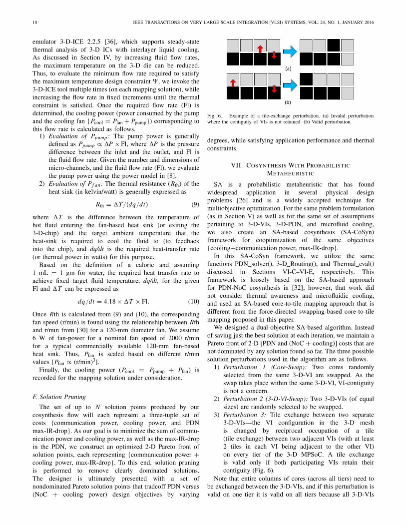
Fig. 6. Example of a tile-exchange perturbation. (a) Invalid perturbationwhere the contiguity of VIs is not retained. (b) Valid perturbation.
degrees, while satisfying application performance and thermalconstraints.
VII. COSYNTHESIS WITH PROBABILISTIC
METAHEURISTIC
SA is a probabilistic metaheuristic that has foundwidespread application in several physical designproblems [26] and is a widely accepted technique formultiobjective optimization. For the same problem formulation(as in Section V) as well as for the same set of assumptionspertaining to 3-D-VIs, 3-D-PDN, and microfluid cooling,we also create an SA-based cosynthesis (SA-CoSyn)framework for cooptimization of the same objectives{cooling+communication power, max-IR-drop}.
In this SA-CoSyn framework, we utilize the samefunctions PDN_solver(), 3-D_Routing(), and Thermal_eval()discussed in Sections VI-C–VI-E, respectively. Thisframework is loosely based on the SA-based approachfor PDN-NoC cosynthesis in [32]; however, that work didnot consider thermal awareness and microfluidic cooling,and used an SA-based core-to-tile mapping approach that isdifferent from the force-directed swapping-based core-to-tilemapping proposed in this paper.
We designed a dual-objective SA-based algorithm. Insteadof saving just the best solution at each iteration, we maintain aPareto front of 2-D [PDN and (NoC + cooling)] costs that arenot dominated by any solution found so far. The three possiblesolution perturbations used in the algorithm are as follows.
1) Perturbation 1 (Core-Swap): Two cores randomlyselected from the same 3-D-VI are swapped. As theswap takes place within the same 3-D-VI, VI-contiguityis not a concern.
2) Perturbation 2 (3-D-VI-Swap): Two 3-D-VIs (of equalsizes) are randomly selected to be swapped.
3) Perturbation 3: Tile exchange between two separate3-D-VIs—the VI configuration in the 3-D meshis changed by reciprocal occupation of a tile(tile exchange) between two adjacent VIs (with at least2 tiles in each VI being adjacent to the other VI)on every tier of the 3-D MPSoC. A tile exchangeis valid only if both participating VIs retain theircontiguity (Fig. 6).
Note that entire columns of cores (across all tiers) need tobe exchanged between the 3-D-VIs, and if this perturbation isvalid on one tier it is valid on all tiers because all 3-D-VIs
KAPADIA AND PASRICHA: SYSTEM-LEVEL COSYNTHESIS FRAMEWORK FOR PDN AND ON-CHIP DATA NETWORKS 11
Algorithm 4 SA-Based Co-Synthesis Framework
are vertically aligned across tiers. The pseudocode for ourSA-CoSyn framework is described in Algorithm 4.
An IMS is arbitrarily generated, which satisfies basic3-D-VI contiguity constraints. The cost of this initial solutionis computed by calling the PDN_solver(), 3-D_Routing(), andThermal_eval() functions. The initial solution now becomesthe current solution in the SA process (Step 1). To initiatethe SA process, the SA-temperature parameter (T ) is set toT init (Step 2). At each iteration, one of the three perturbationsis randomly chosen to perturb the current solution.To generate enough mapping solutions for every 3-D-VIconfiguration, we choose perturbations 1, 2, and 3 withprobabilities 10/13, 1/13, and 2/13, respectively (Step 5).To evaluate the new (perturbed) mapping for communicationpower, cooling power (Pcool) as well as PDN max-IR-drop,our PDN_solver(), 3-D_Routing(), and Thermal_eval() areinvoked (Steps 6–8). Then, the cost of this new solutionis computed (Step 9). Here, the coefficients of the termswith total number of hop-constraint violations (φ) and PDNconstraint violation (φ′) are set to high values, in order topenalize infeasible mapping solutions. If the new solutioncorresponds to no violations and does not have both power costand PDN cost greater than any solution on the current Paretofront (nondominated solution), it is inserted into the Paretofront. Any Pareto solutions that get dominated as a result arediscarded from the front. Thus, the Pareto front of solutions(with nondominated costs), is checked for an update at everyiteration of SA (Step 10). Solutions with better (smaller) costthan the current solution are accepted, and solutions withworse costs are either accepted or rejected according to thefollowing acceptance criteria (Step 11):if (r < exp([cost (current solution)
− cost(new solution)]/T ) ACCEPT = 1
where r is a random number between 0 and 1.
(11)
After every Kmax iterations, the SA temperature is scaledby the parameter δ. Finally, when no new solution is added
to the Pareto front for L number of consecutive SA iterations,the SA process terminates (terminating-condition), and a setof 2-D Pareto design points are produced.
VIII. EXPERIMENTAL STUDIES
A. Experimental Setup
We use the ARM Cortex-A9 multicore processors [24] asthe baseline MPSoC compute cores in our experiments. Theseprocessors support three operating voltage levels (� = 3):0.9, 1, and 1.1 V and corresponding operating frequenciesof 1310, 1550, and 1775 Mz, at the 45-nm process technologynode. The maximum current requirements for the processingcores range from 1 to 4 A, based on the level of com-pute intensity of the tasks assigned to the respective cores.Even though we consider ARM processors in the platformused to evaluate our framework, it should be noted thatour framework is applicable to multicore platforms with anyprocessor architecture, given the operating ranges of supplyvoltages, frequencies, and maximum-powers for the processor.We assume that the rated maximum supply current (and thecorresponding maximum power) of each core is sufficientfor the associated router as well. In our studies, we use a60-core 3-D-mesh for the MPSoC with dimensions 5 × 3 × 4(dimx × dimy × dimz). In addition, we also use a 100-core3-D-mesh of similar homogeneous cores, with dimensions5 × 4 × 5 assuming a 32-nm process technology node. Thevalues of core voltages, frequencies, powers, and area arescaled by the factors of 0.925×, 1.1×, 0.626×, and 0.57×,respectively, to capture the effects of technology scaling(from 45 to 32 nm), as suggested in [14].
Our experiments were conducted using six parallelapplication benchmarks from the SPLASH-2 [21] andPARSEC benchmark suites [19]: streamcluster, ocean, andcholesky for 60-cores (fluidanimate, lu, and vips for 100-cores)of low, medium, and high communication intensities,respectively. Our core graphs are modeled based on intercorecommunication characterizations given in [9]. Each vertex ina core graph corresponds to a core and the edge weights repre-sent intercore communication latency and bandwidth require-ments (based on our observations of traces and communicationpatterns between cores). Our synthesis framework ensuresthat the minimum communication bandwidth constraintsare satisfied, with hop-constraints representing the actualcommunication latency constraints.
The power values of routers and links (32-bit wide) fordifferent voltages, frequencies, and router complexities atvarying communication loads, for 32- and 45-nm processnodes are obtained from ORION 2.0 [16]. As the VLCs andMCFIFOs required to enable error-free interactions betweenVIs incur a power overhead that is proportional to their voltagesupply, we consider the power overhead of these components,with the actual power values based on reported overheadsfrom [15], [22], and [23]. In Thermal_eval(), we conservativelyset the maximum thermal constraint (�) to 75 °C and forthe given mapping solution Fl values are increased in until� is satisfied. The corresponding Ppump and Pfan values arecalculated, as discussed in Section VI-E. Single-phase coolingwith deionized water as coolant material is assumed (similar
12 IEEE TRANSACTIONS ON VERY LARGE SCALE INTEGRATION (VLSI) SYSTEMS, VOL. 24, NO. 1, JANUARY 2016
to [39]). 3-D-ICE assumes identical microchannels, uniformlyplaced, in all microfluidic layers. We set the height and thecross-sectional width of microchannels to 100 and 200 μm,respectively. Microchannels are assumed to be horizontallyseparated by silicon walls, each of width 400 μm (to accom-modate the intertier signal and power TSVs). The temperatureof the coolant fed back into the 3-D-chip is assumed to be fixedat 30 °C ambient, which would satisfy most environments.Our regular 3-D-PDN power grids are modeled based onthe guidelines provided in [4]. For the 60-core mesh, with15 cores on each tier (20 cores for the 100-core mesh), atotal of 240 (320 for 100-core mesh) input power pins areused with n2 = 16 grid nodes for each core. Thus, thetotal number of grid nodes in the entire PDN is equal to960 (1600 for 100-core mesh). For the PDN correspondingto the 60-core mesh, the values of Rh = 40 m� andRv = 80 m� are assumed (based on [4]) for the horizon-tal and vertical branch resistances. For the 100-core mesh,Rh = 28 m� is assumed in accordance to the reduced area,whereas the TSV height is kept unchanged across technologies(as assumed in [13]).
For the implementation of our FDS-CoSyn framework,we generate N IMSs from an equal number of distinct2-D-VI configurations, where N = 66 for the 60-corecase (N = 68 for the 100-core case), is the number of2-D-VI configurations that can be readily found usingAlgorithm 1. Values of 0.3, 0.1, 0.1, and 0.5 are used forα, β2, β1, and γ, respectively. For the SA-based cosynthesisalgorithm, we set Tinit = 100, Kmax = 100, the scaling factorδ = 0.9, and L = 250.
B. Experimental Results
In this section, we present the experimentalresults to highlight several interesting insights of ourproposed framework. Sections VIII-B1 and VIII-B2show the importance of employing PDN awareness andthermal awareness during the synthesis of MPSoCs,respectively. Section VIII-B3 shows the efficacy of theproposed FDS core-mapping approach, in comparison withSA approaches. Section VIII-B4 shows the advantages ofusing our VI-aware routing algorithm in comparison with thetraditional dimension-order routing schemes.
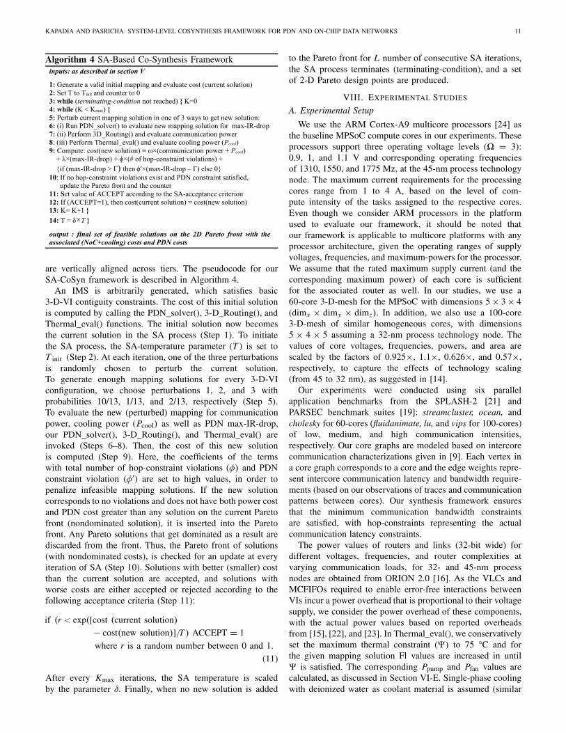
1) Importance of PDN-Awareness: The SA-basedPDN-NoC cosynthesis framework (SA-Basic), introducedin [32] performs PDN-NoC cosynthesis for MPSoCs.To illustrate the importance of PDN-awareness during MPSoCsynthesis, we compare the approach from [32] (SA-Basic),which is PDN-aware with an SA-based PDN-unawareframework (SA-PDN unaware), where the optimizationobjective is primarily to minimize NoC power. The2-D solution space generated by the two frameworksfor six SPLASH-2 and PARSEC benchmarks is shownin Fig. 7, with each candidate solution characterized by itscommunication power and the percentage max-IR-drop in thePDN. The 2-D Pareto front enables the designer to choose adesign point for an appropriate tradeoff between NoC costsand PDN costs. In the SA-PDN-unaware framework, we run
TABLE I
IMPORTANCE OF PDN-AWARENESS: % GROSS IMPROVEMENTS
IN TERMS OF COMMUNICATION POWER AND PDN COST
FOR SA-BASIC VERSUS SA-PDN-UNAWARE
the SA algorithm exactly 10× (starting with different initialmappings) to generate 10 distinct solution points (shown byblack stars in Fig. 7). The PDN unaware approach, which isrepresentative of system-level 3-D NoC synthesis approachesproposed in literature to date, optimizes for NoC power, butthe solutions generated generally have much higher valuesof max-IR-drop. Observe that all of the solution pointsfrom SA-PDN-unaware corresponding to the three 100-corebenchmarks [shown as black stars in Fig. 9(a)–(c)] violate thePDN constraint � (max-IR-drop of 10%), rendering infeasiblefinal solutions.
Each design point on the Pareto front in Fig. 7 representstwo different quantities: 1) communication power and2) percentage max-IR-drop. For a quantitative comparison ofthe results obtained, we select the best point (knee point) oneach Pareto front. The knee point of a 2-D Pareto front ischaracterized by a small improvement in one objective causinga large deterioration in the other objective, thus making itunattractive to move in either direction on the front [10].In our analysis, we define the knee point as the point on thePareto front with the smallest ratio of (improvement in oneobjective)/(deterioration in other objective) when moving ineither directions. The encircled points in Fig. 7 representthe knee points associated with their respective Paretofronts. As the goal of our cosynthesis framework is overalloptimization, evaluating solutions on the basis of only poweror IR drop will be inappropriate. Therefore, while comparingknee-points of two different Pareto fronts, we consider thepercentage gross-improvement: (% improvement in power) +(% improvement in max-IR-drop).
The solution costs associated with the knee-point of eachPareto front in Fig. 7 for SA-Basic and SA-PDN-unaware aretabulated in Table I. Each cell in the first two rows showstwo numbers that represent communication cost (power) andPDN cost (max-IR-drop), respectively. The last row for eachbenchmark suite shows the percentage gross-improvement perbenchmark obtained with SA-Basic over SA-PDN-unaware.This improvement ranges from 5.4% to 13.9%. Thus, it canbe observed from Fig. 7 and Table I that consideringPDN-awareness not only results in feasible PDN solutions butalso solutions with better overall optimality.
2) Importance of Thermal Awareness: To show thesignificance of considering thermal awareness in ourcosynthesis framework, we use a thermal-unaware subset ofour FDS-CoSyn framework (FDS-Basic). FDS-Basic has notemperature optimizing force components (FC3 and FC4),where we use the following coefficient values: 1) α = 0.5;2) β2 = 0; 3) β1 = 0; and 4) γ = 0.5. Therefore, with
KAPADIA AND PASRICHA: SYSTEM-LEVEL COSYNTHESIS FRAMEWORK FOR PDN AND ON-CHIP DATA NETWORKS 13
Fig. 7. Results for SA-PDN-unaware and SA-Basic (PDN-aware) syn-thesis frameworks. (a) streamcluster-100. (b) cholesky-100. (c) ocean-100.(d) fluidanimate-60. (e) lu-60. (f) vips-60.
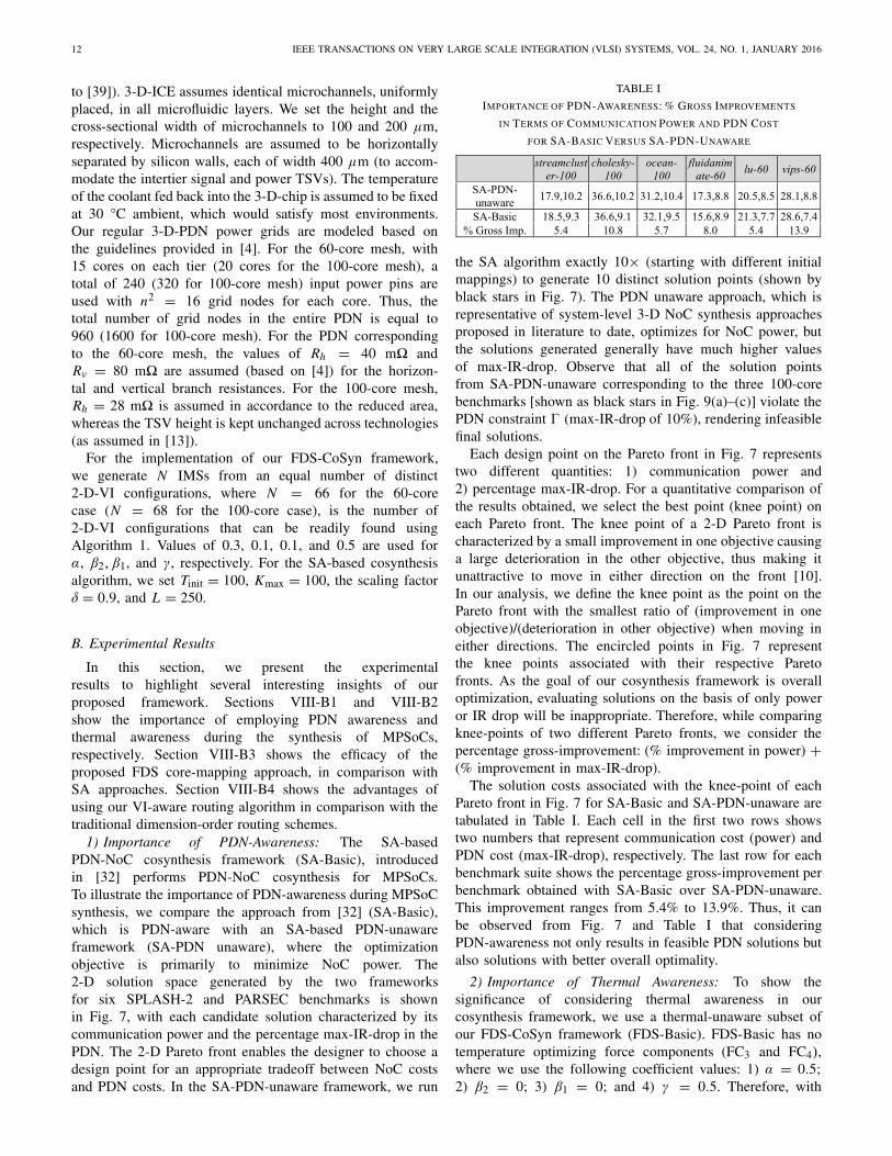
FDS-Basic, communication power is somewhat betteroptimized compared with FDS-CoSyn, while on the otherhand FDS-CoSyn tradesoff communication power with cool-ing power for better overall (communication + cooling) power.The 2-D solution space produced with FDS-Basic andFDS-CoSyn for six benchmarks is shown in Fig. 8, witheach candidate solution characterized by its (communica-tion + cooling) power and the percentage max-IR-drop inthe PDN. By optimizing cooling-power with a slight degra-dation in communication power, it can be observed fromFig. 8 that FDS-CoSyn produces solutions with better overalloptimality compared with the thermal-unaware FDS-Basicframework.
The solution costs associated with the knee-point of eachPareto front in Fig. 8 for FDS-Basic and FDS-CoSyn aretabulated in Table II. The power term in the solution-cost(defined in Section VIII-B1) of each design point now includesthe cooling power in addition to communication power(power = communication power + cooling power). Eachentry in the second and third columns of the table correspondsto {communication + cooling} power and PDN cost.Compared with FDS-Basic, the thermal-awareness inFDS-CoSyn produces improvements in cooling power, by upto 57.8% (as shown in the fourth column of Table II). As thecommunication power with FDS-CoSyn is generally slightlyworse compared with FDS-Basic, lower improvements of upto 13.9% in (communication + cooling) power are obtained
Fig. 8. Results for FDS-Basic (thermal-unaware) and FDS-CoSyn(thermal-aware) cosynthesis frameworks. (a) streamcluster-100. (b) cholesky-100. (c) ocean-100. (d) fluidanimate-60. (e) lu-60. (f) vips-60.
TABLE II
IMPORTANCE OF THERMAL-AWARENESS: PERCENTAGE
GROSS-IMPROVEMENTS IN (COMMUNICATION+COOLING)
POWER AND PDN COST FOR FDS-BASIC
VERSUS FDS-CoSyn
for FDS-CoSyn, as shown in the fifth column. Observethat benchmarks with the lowest communication-intensities(streamcluster-100 and fluidanimate-60) with a much weakerforce-component for communication and a relatively strongthermal component in the FDS algorithm produce higherpower-improvements with the thermal-aware FDS-CoSynframework. In addition, due to the stronger thermal-componentfor these benchmarks, max-IR-drop values obtained usingFDS-CoSyn are slightly higher than that obtained usingFDS-Basic (even with the same value of γ = 0.5). Percentage
14 IEEE TRANSACTIONS ON VERY LARGE SCALE INTEGRATION (VLSI) SYSTEMS, VOL. 24, NO. 1, JANUARY 2016
TABLE III
ALGORITHM COMPARISON: % GROSS-IMPROVEMENTS IN
(COMMUNICATION + COOLING) POWER AND PDN COST
FOR FDS-CoSyn OVER SA-BASIC AND SA-CoSyn
gross-improvements of up to 13.7% (from the last columnof Table II) are obtained for FDS-CoSyn over FDS-Basic.Thus, it can be observed from Fig. 8 and Table II thatconsidering thermal-awareness allows for a reduction incooling power that translates into solutions with better overalloptimality.
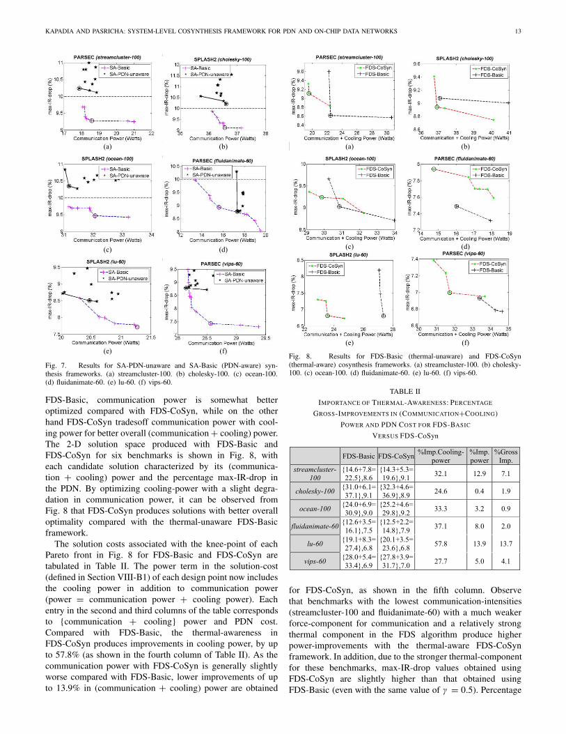
3) Algorithm Comparison: To the best of our knowledge,this is the only work besides [32] that proposes acosynthesis framework to cooptimize the 3-D NoC fabricwith the PDN fabric to produce a more efficient overall3-D MPSoC design. Therefore, in order to evaluate theefficacy of our proposed force-directed heuristic-basedframework (FDS-CoSyn) in comparison with the SA-basedcosynthesis approach in [32] (SA-Basic), we performa comparison study between these frameworks. We also com-pare these frameworks against the SA-based thermal-awareframework (SA-CoSyn) that is also proposed in this paperand described in Section VII. The results of this paper aresummarized in Fig. 9 and Table III. Here, each candidatesolution is characterized by its (communication + cooling)power and the percentage max-IR-drop in the PDN. Notethat the solution points of SA-Basic are transferred fromFig. 7 to the plots of the same benchmark in Fig. 9, withthe added cooling power corresponding to individual solutionpoints, and the new Pareto fronts thus formed are plottedin Fig. 9. Note that our PDN_solver() and 3-D_Routing()in addition to Thermal_eval() are utilized to evaluate themax-IR-drop, communication power, and cooling power in allthree framework implementations.
It can be observed from Fig. 9 and Table III that ourforce-directed swapping algorithm-based FDS-CoSynframework finds excellent mapping solutions correspondingto the given IMSs. Therefore, our approach of applying theswapping algorithm to numerous seeds (initial mappings)generates better overall solutions compared with an SA-basedapproach. In addtion, we observed that the SA algorithmspends considerable time searching for feasible mappingsolutions meeting all hop constraints and the PDN constraint,while FDS-CoSyn has an inherent mechanism for overcominghop-constraint violations and the max-IR-drop optimizingforce component (FC2) ensures that the PDN constraint isalways satisfied. Thus, the force-directed swapping techniquecan optimize the design objectives more efficiently.
Fig. 9. Results for SA-Basic (thermal-unaware), SA-CoSyn, andFDS-CoSyn cosynthesis frameworks. (a) streamcluster-100. (b) cholesky-100.(c) ocean-100. (d) fluidanimate-60. (e) lu-60. (f) vips-60.
Our FDS-CoSyn framework produces solutions with muchbetter overall optimality in terms of cooling costs, commu-nication costs, as well as PDN costs, as shown in Fig. 9.In Table III, the last two rows show the percentage grossimprovements (per benchmark) obtained with FDS-CoSynover SA-Basic and SA-CoSyn FDS-CoSyn produces percent-age gross-improvements ranging from 13.7% to 32.9% overSA-CoSyn, and 15.3% to 35.4% over the thermal-unawareSA-Basic framework.
As discussed earlier, the SA frameworks (SA-Basic andSA-CoSyn) execute until the solution quality fails to improvefor 250 consecutive iterations. On the other hand, we observedthat our FDS framework FDS-CoSyn runs for a maximumof 68 iterations. At each of these iterations, the thermal-unaware (Basic) frameworks execute PDN_solver() and3-D_Routing(), whereas the thermal-aware (CoSyn) frame-work executes Thermal_eval() as well (although in SA-CoSyn,3-D_Routing(), and Thermal_eval() are performed only formapping solutions that satisfy all hop-constraints as well asthe PDN-constraint).
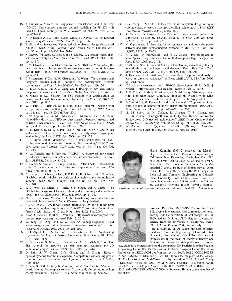
All the synthesis frameworks were simulated on a machinewith Intel Core2-Duo CPU running Linux OS. Table IV showsa comparison of our FDS-CoSyn and SA-CoSyn frameworks,in terms of execution time in seconds. On average, theFDS-CoSyn, produces 12.9× and 4.2× reductions in executiontime over SA-CoSyn and SA-CoSyn. This can be attributed tothe following two factors (in addition to the reduced number
KAPADIA AND PASRICHA: SYSTEM-LEVEL COSYNTHESIS FRAMEWORK FOR PDN AND ON-CHIP DATA NETWORKS 15
TABLE IV
EXECUTION TIMES (IN SECONDS) OF SA-CoSyn
AND FDS-CoSyn, AND PERCENTAGE AVERAGE
REDUCTION IN EXECUTION TIME WITH
FDS-CoSyn OVER SA-CoSyn
of iterations for the FDS frameworks).
1) Unlike in SA-CoSyn, every mapping solution inFDS-CoSyn is optimized for the thermal profile;therefore, the intermediate mapping solutions gen-erated in SA-CoSyn correspond to worse thermalprofiles compared with the final candidate solutionsproduced by FDS-CoSyn. Therefore at each execution ofThermal_eval(), compared with FDS-CoSyn, SA-CoSynrequires on average more 3-D-ICE runs of incrementingflow rates, to satisfy the thermal constraint.
2) The FDS technique generally produces mappingsolutions with shorter communication paths, thusrequiring 3-D_Routing() to evaluate lesser number ofcandidate minimal paths on average.
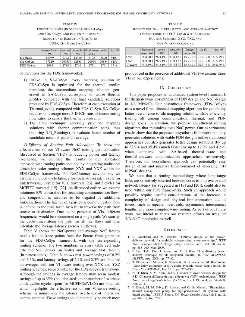
4) Efficacy of Routing Path Allocation: To show theeffectiveness of our VI-aware NoC routing path allocation(discussed in Section VI-D) in reducing power and latencyoverheads, we compare the results of our allocationapproach with routing paths obtained by integrating traditionaldimension-order routing schemes XYX and YXZ within theFDS-CoSyn framework. For NoC-latency calculations, weassume a 5 clock cycle latency for router-traversal, 1 cycle forlink traversal, 1 cycle for VLC traversal [23], and 2 cycles forMCFIFO traversal [15], [22]. As discussed earlier, we assumeminimum BW constraints for sustaining communication flows,and congestion is assumed to be negated by additionallink-insertions. The latency of a particular communication flowis defined as the time taken by a flit to traverse the path fromsource to destination. Due to the presence of VIs, differentfrequencies would be encountered on a single path. We sum-upthe cycle-times along the path for all the flows and thencalculate the average latency (across all flows).
Table V shows the NoC-power and average NoC latencyresults for the knee points from the Pareto front generatedfor the FDS-CoSyn framework with the correspondingrouting scheme. The two numbers in every table cell indi-cate the NoC power (in watts) and average NoC latency(in nanoseconds). Table V shows that power savings of 6.2%and 6.3%, and latency savings of 2.4% and 2.5% are obtainedon average, with our VI-aware routing over XYZ and YXZrouting schemes, respectively, for the FDS-CoSyn framework.Although the savings in average latency may seem modest,savings of up to 35% (not tabulated) in the number of overheadclock cycles (cycles spent for MCFIFOs/VLCs) are obtained,which highlights the effectiveness of our VI-aware-routingscheme in minimizing the latency overheads of interislandcommunication. These savings could potentially be much more
TABLE V
RESULTS FOR NoC POWER (WATTS) AND AVERAGE-LATENCY
(NANOSECOND) FOR FDS-CoSyn WITH DIFFERENT
ROUTING SCHEMES: XYZ, YXZ, AND
OUR-VI-AWARE ROUTING
pronounced in the presence of additional VIs (we assume threeVIs in our experiments).
IX. CONCLUSION
This paper proposes an automated system-level frameworkfor thermal-aware cosynthesis of PDN design and NoC designin 3-D MPSoCs. Our cosynthesis framework (FDS-CoSyn)uses a novel force-directed swapping algorithm for generatingbetter overall core-to-tile mapping solutions, while efficientlytrading off among communication, thermal, and PDNdesign goals. In addition, we propose an efficient routingalgorithm that minimizes total NoC power. Our experimentalresults show that the proposed cosynthesis framework not onlygenerates solutions with viable PDN designs unlike traditionalapproaches but also generates better design solutions (by upto 32.9% and 35.4%) much faster (by up to 12.9× and 4.2×)when compared with SA-based thermal-aware andthermal-unaware cooptimization approaches, respectively.Therefore, our cosynthesis approach can potentially easedesign effort and improve time-to-market of emerging 3-DMPSoC designs.
We note that a routing methodology where long-rangelinks are selectively inserted between cores to improve overallnetwork latency (as suggested in [17] and [20]), could also beused within our FDS frameworks. Such an approach wouldpossibly require careful considerations of the increase incomplexity of design and physical implementation due toissues, such as repeater overheads, asymmetric interconnectlengths, and more complex wire-routing. As part of our futurework, we intend to focus our research efforts on irregular3-D-NoC topologies as well.
REFERENCES
[1] B. Amelifard and M. Pedram, “Optimal design of the power-delivery network for multiple voltage-island system-on-chips,” IEEETrans. Comput.-Aided Design Integr. Circuits Syst., vol. 28, no. 6,pp. 888–900, May 2009.
[2] P. Jain, T.-H. Kim, J. Keane, and C. H. Kim, “A multi-story powerdelivery technique for 3D integrated circuits,” in Proc. ACM/IEEEISLPED, Aug. 2008, pp. 57–62.
[3] T. Okumura, F. Minami, K. Shimazaki, K. Kuwada, and M. Hashimoto,“Gate delay estimation in STA under dynamic power supply noise,” inProc. 15th ASP-DAC, Jan. 2010, pp. 775–780.
[4] N. H. Khan, S. M. Alam, and S. Hassoun, “Power delivery design for3-D ICs using different through-silicon via (TSV) technologies,” IEEETrans. Very Large Scale Integr. (VLSI) Syst., vol. 19, no. 4, pp. 647–658,Apr. 2011.
[5] F. Zanini, M. M. Sabry, D. Atienza, and G. De Micheli, “Hierarchicalthermal management policy for high-performance 3D systems withliquid cooling,” IEEE J. Emerg. Sel. Topics Circuits Syst., vol. 1, no. 2,pp. 88–101, Jun. 2011.
16 IEEE TRANSACTIONS ON VERY LARGE SCALE INTEGRATION (VLSI) SYSTEMS, VOL. 24, NO. 1, JANUARY 2016
[6] A. Sridhar, A. Vincenzi, M. Ruggiero, T. Brunschwiler, and D. Atienza,“3D-ICE: Fast compact transient thermal modeling for 3D ICs withinter-tier liquid cooling,” in Proc. IEEE/ACM ICCAD, Nov. 2010,pp. 463–470.
[7] H. Matsutani et al., “Low-latency wireless 3D NoCs via randomizedshortcut chips,” in Proc. DATE, Mar. 2014, pp. 1–6.
[8] B. Shi and A. Srivastava, “Optimized micro-channel design for stacked3-D-ICs,” IEEE Trans. Comput.-Aided Design Integr. Circuits Syst.,vol. 33, no. 1, pp. 90–100, Jan. 2014.
[9] N. Barrow-Williams, C. Fensch, and S. Moore, “A communication char-acterisation of Splash-2 and Parsec,” in Proc. IEEE IISWC, Oct. 2009,pp. 86–97.
[10] P. M. Chaudhari, R. V. Dharaskar, and V. M. Thakare, “Computing themost significant solution from Pareto front obtained in multi-objectiveevolutionary,” Int. J. Adv. Comput. Sci. Appl., vol. 1, no. 4, Oct. 2010,pp. 63–68.
[11] P. Falkenstern, Y. Xie, Y.-W. Chang, and Y. Wang, “Three-dimensionalintegrated circuits (3D IC) floorplan and power/ground networkco-synthesis,” in Proc. 15th ASP-DAC, Jan. 2010, pp. 169–174.
[12] H.-T. Chen, H.-L. Lin, Z.-C. Wang, and T. Hwang, “A new architecturefor power network in 3D IC,” in Proc. DATE, Mar. 2011, pp. 1–6.
[13] K. Ghosh et al., “Strategy for TSV scaling with consideration onthermo-mechanical stress and acceptable delay,” in Proc. 7th IMPACT,Oct. 2012, pp. 49–51.
[14] W. Huang, K. Rajamani, M. R. Stan, and K. Skadron, “Scaling withdesign constraints: Predicting the future of big chips,” IEEE Micro,vol. 31, no. 4, pp. 16–29, Jul./Aug. 2011.
[15] R. W. Apperson, Z. Yu, M. J. Meeuwsen, T. Mohsenin, and B. M. Baas,“A scalable dual-clock FIFO for data transfers between arbitrary andhaltable clock domains,” IEEE Trans. Very Large Scale Integr. (VLSI)Syst., vol. 15, no. 10, pp. 1125–1134, Oct. 2007.
[16] A. B. Kahng, B. Li, L.-S. Peh, and K. Samadi, “ORION 2.0: A fastand accurate NoC power and area model for early-stage design spaceexploration,” in Proc. DATE, Apr. 2009, pp. 423–428.
[17] U. Y. Ogras and R. Marculescu, “‘It’s a small world after all’: NoCperformance optimization via long-range link insertion,” IEEE Trans.Very Large Scale Integr. (VLSI) Syst., vol. 14, no. 7, pp. 693–706,Jul. 2006.
[18] N. A. Kapadia and S. Pasricha, “VISION: A framework for voltageisland aware synthesis of interconnection networks-on-chip,” in Proc.21st GLSVLSI, 2011, pp. 31–36.
[19] C. Bienia, S. Kumar, J. P. Singh, and K. Li, “The PARSEC benchmarksuite: Characterization and architectural implications,” in Proc. 17thPACT, Oct. 2008, pp. 72–81.
[20] A. Ganguly, K. Chang, S. Deb, P. P. Pande, B. Belzer, and C. Teuscher,“Scalable hybrid wireless network-on-chip architectures for multicoresystems,” IEEE Trans. Comput., vol. 60, no. 10, pp. 1485–1502,Oct. 2011.
[21] S. C. Woo, M. Ohara, E. Torrie, J. P. Singh, and A. Gupta, “TheSPLASH-2 programs: Characterization and methodological considera-tions,” in Proc. 22nd Annu. ISCA, Jun. 1995, pp. 24–36.
[22] M. E. S. Elrabaa, “A new FIFO for transferring data between twounrelated clock domains,” Int. J. Electron., to be published.
[23] P. Zhao et al., “Low-power clocked-pseudo-NMOS flip-flop for levelconversion in dual supply systems,” IEEE Trans. Very Large ScaleIntegr. (VLSI) Syst., vol. 17, no. 9, pp. 1196–1202, Sep. 2009.
[24] ARM Cortex-A9. [Online]. Available: http://www.arm.com/products/processors/selector.php, accessed Feb. 12, 2015.
[25] W. Jang, D. Ding, and D. Z. Pan, “A voltage-frequency islandaware energy optimization framework for networks-on-chip,” in Proc.IEEE/ACM ICCAD, Nov. 2008, pp. 264–269.
[26] C. J. Alpert, D. P. Mehta, and S. S. Sapatnekar, Eds., Handbook ofAlgorithms for Physical Design Automation. Boca Raton, FL, USA:CRC Press, 2009.
[27] C. Seiculescu, S. Murali, L. Benini, and G. De Micheli, “SunFloor3D: A tool for networks on chip topology synthesis for 3Dsystems on chips,” in Proc. DATE, Apr. 2009, pp. 9–14.
[28] D. Shin, S. W. Chung, E.-Y. Chung, and N. Chang, “Energy-optimal dynamic thermal management: Computation and cooling powerco-optimization,” IEEE Trans. Ind. Informat., vol. 6, no. 3, pp. 340–351,Aug. 2010.
[29] X. Wei, G. Goth, P. Kelly, R. Zoodsma, and A. VanDeventer, “Air-waterhybrid cooling for computer servers: A case study for optimum coolingenergy allocation,” in Proc. IEEE ITherm, May 2014, pp. 568–573.
[30] J.-Y. Chang, H. S. Park, J. I. Jo, and S. Julia, “A system design of liquidcooling computer based on the micro cooling technology,” in Proc. IEEE10th Itherm, May/Jun. 2006, pp. 157–160.
[31] S. Pasricha, “A framework for TSV serialization-aware synthesis ofapplication specific 3D networks-on-chip,” in Proc. 25th Int. Conf.VLSID, Jan. 2012, pp. 268–273.
[32] N. Kapadia and S. Pasricha, “A co-synthesis methodology for powerdelivery and data interconnection networks in 3D ICs,” in Proc. 14thISQED, 2013, pp. 73–79.
[33] W.-P. Lee, D. Marculescu, and Y.-W. Chang, “Post-floorplanningpower/ground ring synthesis for multiple-supply-voltage designs,” inProc. ISPD, 2009, pp. 5–12.
[34] Q. Zhou, J. Shi, B. Liu, and Y. Cai, “Floorplanning considering IR dropin multiple supply voltages island designs,” Trans. Very Large ScaleIntegr. (VLSI) Syst., vol. 19, no. 4, pp. 638–646, Apr. 2011.
[35] S. Kose and E. G. Friedman, “Fast algorithms for power grid analysisbased on effective resistance,” in Proc. IEEE ISCAS, May/Jun. 2010,pp. 3661–3664.
[36] “LP_solve open-source tool,” 3D-ICE Open-Source Tool. [Online].Available: http://esl.epfl.ch/3d-ice.html, accessed Feb. 12, 2015.
[37] A. K. Coskun, J. Meng, D. Atienza, and M. M. Sabry, “Attaining single-chip, high-performance computing through 3D systems with activecooling,” IEEE Micro, vol. 31, no. 4, pp. 63–75, Jul./Aug. 2011.
[38] D. Starobinksi, M. Karpovsky, and L. A. Zakrevski, “Application of net-work calculus to general topologies using turn-prohibition,” IEEE/ACMTrans. Netw., vol. 11, no. 3, pp. 411–421, Jun. 2003.
[39] M. M. Sabry, A. K. Coskun, D. Atienza, T. S. Rosing, andT. Brunschwiler, “Energy-efficient multiobjective thermal control forliquid-cooled 3-D stacked architectures,” IEEE Trans. Comput.-AidedDesign Integr. Circuits Syst., vol. 30, no. 12, pp. 1883–1896, Dec. 2011.
[40] Introduction to Lp_Solve 5.5.2.0. [Online]. Available:http://lpsolve.sourceforge.net/5.5/, accessed Feb. 12, 2015.
Nishit Kapadia (SM’12) received the Master’sDegree in Electrical and Computer Engineering atCalifornia State University, Northridge, CA, USAin 2005. From 2006 to 2008, he worked as a VLSIfaculty at the Department of Electronics, Sardar Val-labhbhai National Institute of Technology at Surat,India. He is currently pursuing the Ph.D. degree inElectrical and Computer Engineering at ColoradoState University, Fort Collins, CO, USA. Hisresearch interests are CAD for multi-core 2D and3D Systems, networks-on-chip, power-, thermal-,
variation-, and reliabilty-aware design methodologies, and VLSI Automation.
Sudeep Pasricha (M’02–SM’13) received theB.E. degree in electronics and communication engi-neering from Delhi Institute of Technology, India, in2000, and the M.S. and Ph.D. degrees in computerscience from the University of California, Irvine,CA, USA, in 2005 and 2008, respectively.
He is currently an Associate Professor of Elec-trical and Computer Engineering at Colorado StateUniversity, Fort Collins, CO, USA. His researchinterests are in the areas of energy efficiency andfault tolerant design for high performance comput-
ing, embedded systems, and mobile computing. Dr. Pasricha is or has been anOrganizing Committee Member and/or Technical Program Committee mem-ber of various IEEE/ACM conferences such as DAC, DATE, CODES+ISSS,NOCS, ISQED, VLSID, and GLSVLSI. He was the recipient of the GeorgeT. Abell Outstanding Mid-Career Faculty Award in 2014, AFOSR YoungInvestigator Award in 2013, ACM SIGDA Technical Leadership Awardin 2012, and Best Paper Awards at the IEEE AICCSA 2011, IEEE ISQED2010 and ACM/IEEE ASPDAC 2006 conferences. He is a senior member ofthe IEEE.