ic-htg power cw laser diode driver · ate an external laser or led diode with an external ... ic...
TRANSCRIPT

preliminary
preliminary iC-HTGPOWER CW LASER DIODE DRIVER
Rev A1, Page 1/40
FEATURES
CW operation with external driver transistor 3.3 to 24 V power supply Analog modulation frequency of up to 50 kHz Internal programmable logarithmic monitor resistor Operating point setup with a logarithmic resolution of 10 bits Current or Power control mode (ACC/APC) configurable A/D converters for analog signals monitoring Serial programming interface (SPI or I2C compliant) Configuration RAM content integrity monitored. Optimized for both N-type and P-type laser diodes Low drop linear regulator for 3.3 V Low current standby mode Temperature monitor Temperature range of -40 to 85 °C
APPLICATIONS
Commercial LED/Laser diodemodules
Safety related CW laser diodedrivers
Structured-light 3D illumination Laser diode stack control Optical amplification Optical pumping
PACKAGES
QFN24 4 mm x 4 mm
BLOCK DIAGRAM
-
+
iC-HTG
-+
+-
POWERLASERDIODEDRIVER
CURRENTCHANNEL
LASERREGULATOR
VDDUNDERVOLTAGE
POWERCHANNEL
LASERCHANNEL
VDDREGULATOR
VBUNDERVOLTAGE
OVERCURRENT
TEMPERATURE
x2,x5,x10,x50
MONITOR8Bit
WATCHDOG
REGISTERS
IODRIVERS
OSCILLATOR
CGAIN(1:0)
ADCC(2:0)
SCLK/SCL
RDCO(5:0)
INTEGRITY
MISO/SDA
CONTROL
TEMP(7:0)
RMD(7:0)
ADC(9:8)
ADC(7:0)
REF(7:0)
REF(9:8)
MOSI/A0
CFGTIMO
ILIM(7:0)
OSCERR
MEMERR
NCS/A1
CHECK
EPNNP
SPI/I2C
LASER
SLAVE
NSTBY
3...24V
CVDD
MCVRTIMERCheck
NCHK
T.PAD
CVBL
10Bit
10Bit
EACC
VRP/30VRN/30
MOD
PDOx
DCOANIN
MCH
RMC
DCO
VBL/30
0x1F
VDD
0x3F
GND
RAM
GND
RAM
0x03
0x10
0x04
0x11
CVB
MCL
0x02
0x15
0x12
MDL
0x15
0x130x300x100x14
VRP
VRN
8Bit
REF
8Bit
REF
ENAM
VDD/8
VBLVBL
VB/30
OVC
VREF
VCU
OVT
255
CVDD
+
CVBL+
+
CVBCI
MD
ANIN
MC
INS
MR
CIL
OVC
EC
VCU
MDL
VB VB
--
-
=1
MC
=1
ID
CICI
D
D
DA
R
A
A+
+
7
0
0
1
0
10
0
1
-
-
EPNNPVCU
VRN
NSTBY
+
MR
MCH
MDL
+
VBL
NCS/A1
ID
VB
MOD
MISO/SDA
CI-
Check
VCU
MC
EACC
ENAM
VRN/30
VDD
VB/30
3...24VVB
+
OVC
MC
-
DCO
VRP/30NCHK
T.PAD
VDD/8
VRP
VBL/30
ANIN
INS
VBL
-
GND
MCL
EC
CIL
MOSI/A0
ANIN
VREFREF
MD
GND
SCLK/SCL
MCVRMDL
Copyright © 2017 iC-Haus http://www.ichaus.com

preliminary
preliminary iC-HTGPOWER CW LASER DIODE DRIVER
Rev A1, Page 2/40
DESCRIPTION
The CW power laser diode driver iC-HTG can oper-ate an external laser or LED diode with an externalpower transistor and has automatic current (ACC) andpower (APC) control functionality. All parameters, in-cluding the internal reference voltages, are set viaserial communication (I2C or SPI). A 10-bit resolutionD/A converter with logarithmic characteristic is usedto set the operating point of the laser or LED. Thisallows an operating point resolution better than 1%.In APC mode, the monitor diode photocurrent is usedto track the optically emitted power of the laser diode.The voltage present over a resistor through which thephotocurrent flows is used for feedback in the controlloop. An 8-bit internal programmable logarithmic mon-itor resistor (PLR) or an external monitor resistor canbe selected to close the control loop. The PLR rangesfrom 100Ω to 500 kΩ with a step width of less than5%. In ACC mode, the laser diode current can bemeasured by means of a low impedance shunt resis-tor. The output power can be analog modulated witha frequency of up to 50 kHz. iC-HTG allows the laserchannel to be disabled when an overcurrent thresholdhas been exceeded. The overcurrent threshold is pro-grammable using an 8-bit linear D/A converter. Thetemperature monitor measures the internal chip tem-perature. iC-HTG disables the laser channel when
overtemperature is detected. A variety of voltagescan be measured with a 10-bit A/D converter. Thefollowing voltages can be measured:
• V(VB)• V(VBL)• V(VDD)• V(ANIN)• V(MC)• V(MDL)• V(VRP)• V(VRN)
The current output pin DCO can be used to adjustan external DC/DC converter. Controlling the DC/DCoutput voltage may optimize the power dissipationof the whole system to extend battery life, for exam-ple. In standby mode, iC-HTG has a very low currentconsumption (typ. < 10µA) while retaining its config-uration. The device features for safe operation are:
• Configuration RAM content integrity monitored• Tri-state configuration pins• Write protection in operating mode• Safe power-up state

preliminary
preliminary iC-HTGPOWER CW LASER DIODE DRIVER
Rev A1, Page 3/40
CONTENTS
PACKAGING INFORMATION 4PIN CONFIGURATION QFN24 4 mm x 4 mm
(topview) . . . . . . . . . . . . . . . . . 4PACKAGE DIMENSIONS QFN24-4x4 . . . . 5
ABSOLUTE MAXIMUM RATINGS 6
THERMAL DATA 6
ELECTRICAL CHARACTERISTICS 7
OPERATING REQUIREMENTS 10SPI and I2C Interface . . . . . . . . . . . . . 10
STANDBY 11
OPERATION MODE 11Laser enabling and error handling . . . . . . 11
CONTROL MODES AND LASER DIODE/LEDTYPES 13CI capacitor . . . . . . . . . . . . . . . . . . . 13ACC mode . . . . . . . . . . . . . . . . . . . 13ACC mode monitoring the optical power . . . 14APC mode . . . . . . . . . . . . . . . . . . . 14APC mode monitoring the laser current . . . 15Other functions . . . . . . . . . . . . . . . . . 15
OVERCURRENT MONITOR 16
WATCHDOG TIMER 16
SERIAL COMMUNICATION INTERFACES 17Communication modes . . . . . . . . . . . . 17SPI slave interface . . . . . . . . . . . . . . . 17I2C slave interface . . . . . . . . . . . . . . . 17
8-BIT INTERNAL PROGRAMMABLELOGARITHMIC MONITOR RESISTORS 19
10-BIT LOGARITHMIC D/A CONVERTER 20
10-BIT LINEAR A/D CONVERTER 21
ANIN GENERAL PURPOSE IO PIN 22
DC/DC CONVERTER OPTIMIZATION 23DC/DC step down operation:
regulation at voltages lower than powersupply . . . . . . . . . . . . . . . . . . . 23
DC/DC step up operation: regulation atvoltages higher than power supply . . . 24
Extension of system working voltage range . 24Efficiency enhancement . . . . . . . . . . . . 24
ANALOG MODULATION 25Setting Current Modulation . . . . . . . . . . 25
TEMPERATURE MONITOR AND PROTECTION 27
CONFIGURATION MODE AND MEMORYINTEGRITY MONITOR 28Register map description . . . . . . . . . . . 28Read-only registers with values or states . . 29Configuration page (integrity monitored) . . . 29Validation page . . . . . . . . . . . . . . . . . 29Possible start-up sequence: . . . . . . . . . . 29
REGISTER OVERVIEW 30
PARAMETERS 31Status . . . . . . . . . . . . . . . . . . . . . . 31Channel configuration registers . . . . . . . . 33
EXAMPLES OF CONFIGURATION 35ACC mode . . . . . . . . . . . . . . . . . . . 35APC mode . . . . . . . . . . . . . . . . . . . 36APC mode with current monitor or ACC mode
with optical power monitor . . . . . . . . 37
DESIGN REVIEW: Notes On Chip Functions 39
REVISION HISTORY 39
preliminary
preliminary iC-HTGPOWER CW LASER DIODE DRIVER
Rev A1, Page 4/40
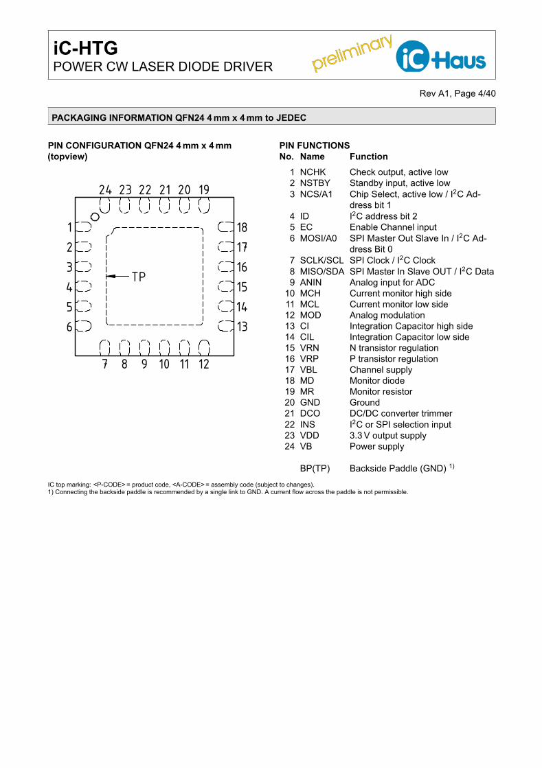
PACKAGING INFORMATION QFN24 4 mm x 4 mm to JEDEC
PIN CONFIGURATION QFN24 4 mm x 4 mm(topview)
123456
7 8 9 10 11 12
131415161718
192021222324
TP
PIN FUNCTIONSNo. Name Function
1 NCHK Check output, active low2 NSTBY Standby input, active low3 NCS/A1 Chip Select, active low / I2C Ad-
dress bit 14 ID I2C address bit 25 EC Enable Channel input6 MOSI/A0 SPI Master Out Slave In / I2C Ad-
dress Bit 07 SCLK/SCL SPI Clock / I2C Clock8 MISO/SDA SPI Master In Slave OUT / I2C Data9 ANIN Analog input for ADC
10 MCH Current monitor high side11 MCL Current monitor low side12 MOD Analog modulation13 CI Integration Capacitor high side14 CIL Integration Capacitor low side15 VRN N transistor regulation16 VRP P transistor regulation17 VBL Channel supply18 MD Monitor diode19 MR Monitor resistor20 GND Ground21 DCO DC/DC converter trimmer22 INS I2C or SPI selection input23 VDD 3.3 V output supply24 VB Power supply
BP(TP) Backside Paddle (GND) 1)
IC top marking: <P-CODE> = product code, <A-CODE> = assembly code (subject to changes).1) Connecting the backside paddle is recommended by a single link to GND. A current flow across the paddle is not permissible.
preliminary
preliminary iC-HTGPOWER CW LASER DIODE DRIVER
Rev A1, Page 5/40
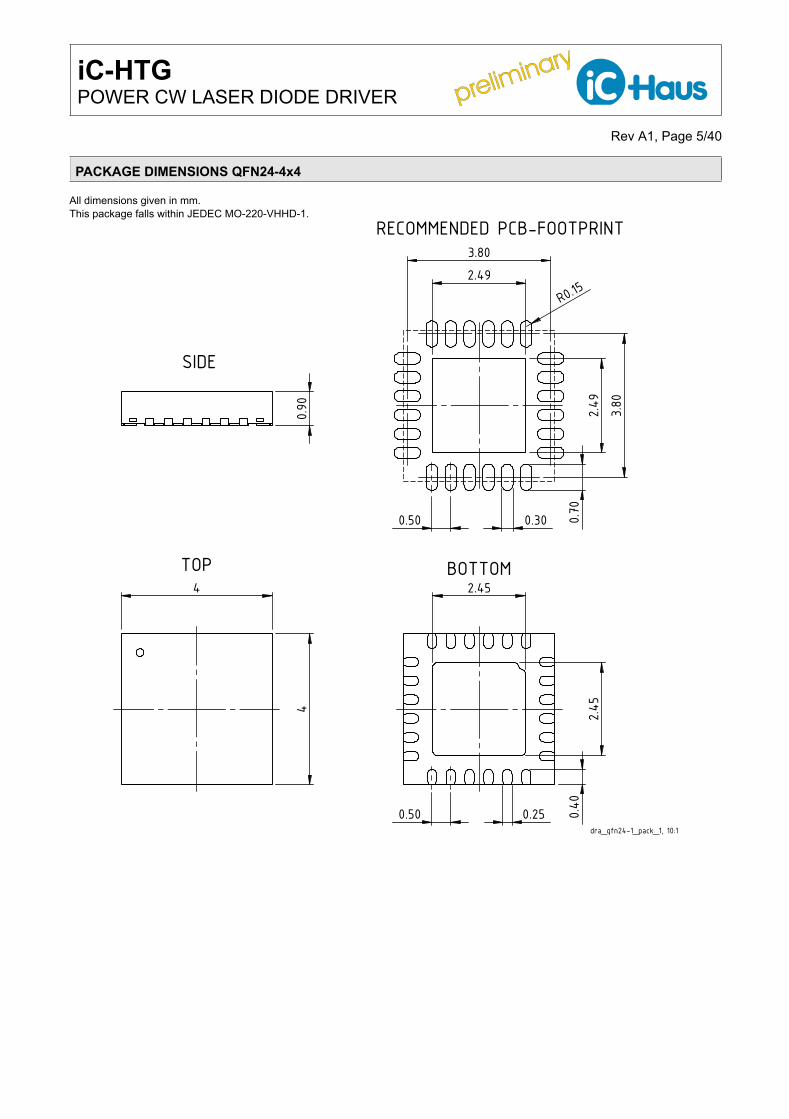
PACKAGE DIMENSIONS QFN24-4x4
All dimensions given in mm.This package falls within JEDEC MO-220-VHHD-1.
4
40.90
SIDE
0.250.50
2.452.45
0.40
BOTTOM
2.49
3.80
2.49
3.80
R0.15
0.50 0.30 0.70
RECOMMENDED PCB-FOOTPRINT
dra_qfn24-1_pack_1, 10:1
TOP

preliminary
preliminary iC-HTGPOWER CW LASER DIODE DRIVER
Rev A1, Page 6/40
ABSOLUTE MAXIMUM RATINGS
These ratings do not imply permissible operating conditions; functional operation is not guaranteed. Exceeding these ratings may damagethe device.Item Symbol Parameter Conditions UnitNo. Min. Max.G001 VB Voltage at VB, VBL -0.3 30 VG002 I(VB) Current in VB, VBL -20 50 mAG003 VDD Voltage at VDD -0.3 5.5 VG004 I(VDD) Current in VDD -20 1 mAG005 V() Voltage at DCO, ANIN, SCLK/SCL,
MISO/SDA, MOSI/A0, NCS/A1, DCO,INS, NCHK, CI, MOD
-0.3 5.5 V
G006 V() Voltage at VRP, VRN, MCH, MCL,NSTBY
30 V
G007 I() Current in DCO, ANIN, SCLK/SCL,MISO/SDA, MOSI/A0, NCS/A1, DCO,INS, NCHK, CI, VRP, VRN, MCH, MCL,NSTBY
-20 20 mA
G008 V() Voltage at CIL -0.3 0.5 VG009 I(CIL) Current in CIL DC current -900 1 mAG010 Vd() ESD Susceptibility at all pins HBM 100 pF discharged through 1.5 kΩ 2 kVG011 Tj Operating Junction Temperature -40 85 °CG012 Ts Storage Temperature Range -40 150 °C
THERMAL DATA
Operating Conditions: VB = 3 . . . 24 V (referenced to GND)Item Symbol Parameter Conditions UnitNo. Min. Typ. Max.
T01 Ta Operating Ambient Temperature Range -40 85 °CT02 Rthja Thermal Resistance Chip/Ambient Mounted on PCB 25 K/WT03 RthjTP Thermal Resistance Chip/Thermal Pad 4 K/W
All voltages are referenced to ground unless otherwise stated.All currents flowing into the device pins are positive; all currents flowing out of the device pins are negative.

preliminary
preliminary iC-HTGPOWER CW LASER DIODE DRIVER
Rev A1, Page 7/40
ELECTRICAL CHARACTERISTICS
Operating Conditions: VB = 3 . . . 24 V (relative to GND), Tj = -40 . . . 125 °C unless otherwise statedItem Symbol Parameter Conditions UnitNo. Min. Typ. Max.GeneralFunctionality and parameters beyond the operating conditions (with reference to independent voltage supplies, for instance) are to beverified within the individual application using FMEA methods.001 VB Permissible Supply Voltage Relative to GND 3 24 V002 I(VB) Standby Current at VB V(NSTBY) ≤ 0.4 V,
VB = 3. . . 11 V 10 µAVB = 11. . . 24 V 30 µA
003 I(VBL) Standby Current at VBL V(NSTBY) ≤ 0.4 V,VBL = 3. . . 11 V 5 µAVBL = 11. . . 24 V 10 µA
004 I(VB) Supply Current at VB No load, EC, NSTBY = hi 5 mA005 I(VBL) Supply Current at VBL No load, EC, NSTBY = hi 25 mA006 V(VB)on Turn-on threshold at VB, VBL Increasing VB, VBL 1 2.9 V007 V(VB)off Turn-off threshold at VB, VBL Decreasing VB, VBL 0.8 2.6 V008 V(VB)Hys Power-on hysteresis at VB, VBL 20 250 mV009 V(VDD)on Turn-on threshold Increasing VDD 1.3 2.4 V010 V(VDD)off Turn-off threshold Decreasing VDD 1.2 2.3 V011 V(VDD)Hys Power-on hysteresis 20 250 mV012 V(VB)INITR RAM memory reset during
Stand-ByNSTBY = lo 0.85 1.4 V
013 RCIL() Resistor between GND and CIL 20 Ω
014 Vc()lo Clamp Voltage lo at VB,VBL, VDD, NCHK, NCS/A1,MISO/SDA, MOSI/A0,SCLK/SCL, INS, NSTBY, EC,DCO, CI, MD, MR, MCH, MCL,VRP, VRN, MOD
I() = -10 mA -1.6 -0.3 V
Transistor Driver VRx, CIx, MCx, MR, MD101 C(CI) Required capacitor at CI CW 1000 pF
Analog Modulation 80 pF102 I(CI) Charge Current at CI V(CI) = 0 V, CI regulated -30 -5 µA103 V(MCx) Permisible Voltage at MCH, MCL EC = hi, NSTBY = hi
MCVR = lo 0 5 VMCVR = hi VBL-5 VBL V
104 Tci Permisible Voltage at MR, MD EC = hi, NSTBY = hiEPNNP = lo 0 1.2 VEPNNP = hi VDD-1.2 VDD V
105 I(VRx)max Short Circuit Current at VRP,VRN
EC = hi, NSTBY = hiV(VRP) = 1.5 V . . . VBL V -200 mAV(VRN) = 1.5 V . . . VBL V; VRNHR = hi 200 mAV(VRN) = 0 V . . . VBL-1.5 V; VRNHR = lo 200 mA
106 V(VRP) Voltage output range |I(VRP)| < 1mA 1 VBL V
107 V(VRN) Voltage output range |I(VRN)| < 1mAVRNHR = lo 0 VBL-1.5 VVRNHR = hi 1 VBL V
108 Ten Time to laser enabled NSTBY lo → hi, no load at VDD, 1.3 msV(VDD) 0 to 90 %,CVDD = 1µF
Programmable Resistor201 Rmda Resistor at MD and MR pin RMD(7:0) = 0xFF, DISP = 0 350 500 650 kΩ
RMD(7:0) = 0x00, DISP = 0 0.154 0.220 0.286 kΩ202 Tk Temperature coefficient -500 ppm/K

preliminary
preliminary iC-HTGPOWER CW LASER DIODE DRIVER
Rev A1, Page 8/40
ELECTRICAL CHARACTERISTICS
Operating Conditions: VB = 3 . . . 24 V (relative to GND), Tj = -40 . . . 125 °C unless otherwise statedItem Symbol Parameter Conditions UnitNo. Min. Typ. Max.
203 ∆R Resistor increment ∆R = R(n+1)−R(n)R(n) 1 3.3 7 %
204 Ileak(MDA) MD, MR leakage current DISP = 1 -2 2 µAD/A Converter301 RES(DAC) D/A Converter Resolution 10 bit302 ∆V Voltage increments ∆V = V(n+1)−V(n)
V(n) 0.05 0.235 1 %303 V(DAC) D/A Converter REF(9:0) = 0x000 lowest value 0.09 0.10 0.12 V
REF(9:0) = 0x3FF highest value 1.00 1.10 1.25 V304 V(REF) D/A Converter V(MOD)=1.1V, Analog Modulation Enabled
REF(9:0) = 0x000 lowest value 0.09 0.10 0.12 VREF(9:0) = 0x3FF highest value 1.00 1.10 1.25 V
305 G() Gain Factor ACC modeCGAIN(1:0) = 00 1.5 2 2.5CGAIN(1:0) = 01 3 5 7CGAIN(1:0) = 10 7 10 13CGAIN(1:0) = 11 43 50 57
Check Output NCHK401 Vs()lo Saturation Voltage lo at NCHK I(NCHK) = 1.0 mA 0.4 V402 Isc()lo Short Circuit Current lo at NCHK V(NCHK) = 0.4 . . . 3.3 V 9 33 mA403 Ilk() Leakage Current at NCHK NCHK = 1;
V(NCHK) = 0 . . . 5.5 V -10 10 µASeries Regulator Output VDD501 V(VDD) Regulated output voltage I(VDD) = -10 . . . 0 mA
NSTBY = hi3 3.5 V
502 V(VB,VDD) Voltage Drop between VB andVDD
VB=3 V , I(VDD) = -10 . . . 0 mANSTBY = hi
300 630 mV
503 C(VDD) Capacitor at VDD Ri(C) < 1Ω 1 3.3 µF504 Tvdd Settling time VDD NSTBY lo → hi, no load at VDD,
V(VDD) 0 to 90 %CVDD = 1µF
1 ms
505 Isc(VDD) Short circuit current at VDD VDD Connected to GND -125 mADigital inputs/output NCS/A1, MISO/SDA, MOSI/A0, SCLK/SCL, ID, NSTBY, EC, ANIN601 Vt()hi Input Threshold Voltage hi at
NCS/A1, MISO/SDA, MOSI/A0,SCLK/SCL, ID, NSTBY, EC,ANIN
MISO/SDA as input with INS = hi 2 V
602 Vt()lo Input Threshold Voltage lo atNCS/A1, MISO/SDA, MOSI/A0,SCLK/SCL, ID, NSTBY, ANIN,EC, ANIN
MISO/SDA as input with INS = hi 0.7 V
603 Vt()hys Hysteresis at NCS/A1,MISO/SDA, MOSI/A0,SCLK/SCL, ID, NSTBY, ANIN,EC
Vt()hys = Vt()hi - Vt()lo 50 mV
604 Ipd() Pull-Down Current at MOSI/A0,EC
V() = 0.4 V . . . VDD 1 50 µA
605 Ipd() Dynamic Pull-Down Current atNSTBY
V() = 0.4 V . . . Vt()hi 2 50 µAV() = Vt(hi) . . . VB 1 15 µA
606 Rpu() Pull-Up Resistor at NCS/A1,SCLK/SCL
80 150 260 kΩ
607 Rpu() Pull-Up Resistor at MISO/SDA INS = lo 8 20 50 kΩINS = hi 53 100 174 kΩ
608 Er() Safe enable threshold voltage atINS
Rising 52 54 56 % VDDFalling 30 32 34 % VDD
609 Voc() Open Circuit Voltage at INS 39 41 43 % VDD

preliminary
preliminary iC-HTGPOWER CW LASER DIODE DRIVER
Rev A1, Page 9/40
ELECTRICAL CHARACTERISTICS
Operating Conditions: VB = 3 . . . 24 V (relative to GND), Tj = -40 . . . 125 °C unless otherwise statedItem Symbol Parameter Conditions UnitNo. Min. Typ. Max.
610 Ri() Internal Resistance at INS 170 250 330 kΩ611 Isc()lo Short Circuit current lo at
MISO/SDAINS = lo, V(MISO/SDA) = 5.5 V -40 -4 mA
612 Vs()lo Saturation Voltage lo atMISO/SDA
INS = lo, I(MISO/SDA) = 2 mA 0.4 V
613 Isc()lo Short Circuit current lo at ANIN ANIN as output, V(ANIN) = 5.5 V -40 -4 mA614 Vs()lo Saturation Voltage lo at ANIN ANIN as output, I(ANIN) = 2 mA 0.4 V
A/D Converter701 Ton Converter initialization time ENAD changes from 0 to 1 500 µs
702 Tconv Conversion time 140 µs703 RES(ADC) A/D Converter Resolution 10 bit704 RAC Relative Accuracy -1 +1 LSB705 VZS() Zero Scale Voltage ADC(9:0) = 0x000 0 V706 VFS() Full Scale Voltage ADC(9:0) = 0x3FF 1.0 1.1 1.2 V707 VDDM() VDD Measurement VDD=3.3 V, ADCC(2:0)= 000 334 368 402 LSB708 VBLM() VBL Measurement VBL=24 V, ADCC(2:0) = 001 654 720 786 LSB709 VBM() VB Measurement VB=24 V, ADCC(2:0) = 010 654 720 786 LSB710 MDLM() MDL Measurement |V(MD)-V(MR)|=0.5 V, ADCC(2:0) = 011 413 455 497 LSB711 MCM() V(MCH)-V(MCL)Measurement V(MCH) < 3 V, V(MCH)-V(MCL)=0.25 V,
CGAIN(1:0)=000 ADCC(2:0) = 100400 441 482 LSB
712 VRNM() VRN Measurement VRN=VBL=VB= 12 V, ADCC(2:0) = 101 330 365 402 LSB713 VRPM() VRP Measurement VRP = 24 V, ADCC(2:0) = 110 658 724 790 LSB714 ANINM() ANIN Measurement ANIN = 0.5 V, ADCC(2:0) = 111 409 451 493 LSB
OvertemperatureB01 Toff Overtemperature Shutdown Rising temperature 130 170 °CB02 Ton Overtemperature Release Falling temperature 120 160 °CB03 Thys Hysteresis Toff − Ton 3 °C
Temperature MonitorC01 Trange Temperature Measurement
Range-40 125 °C
C02 Tresol Temperature Measurement Reso-lution
1 °C
C03 TEMP Temperature Value Ranges Tj = 60 °C 100 125 LSBTj = 0 °C 40 60 LSB
DCO OutputD01 Isc()hi DCO Output Current V(VDD) = 3...3.5 V, V(DCO) < 1.4 V,
RDCO = 0x3F-175 -130 -85 µA
D02 Ileak Leakage Current at DCO RDCO = 0x00 or NSTBY = lo,V(DCO) = 0 . . . 5.5 V
-1 1 µA
D03 I(DCO)LSB I(DCO) Resolution V(DCO) < 1.4 V 1.3 2 2.7 µAOscillatorE01 F(osc) Oscillator Frequency NSTBY = hi 100 200 400 kHzE02 T(CFGTIMO)Configuration Mode Timeout MODE(1:0) = 10 40 82 164 msE03 tWDT Watchdog Timeout NSTBY = hi 20 120 µs

preliminary
preliminary iC-HTGPOWER CW LASER DIODE DRIVER
Rev A1, Page 10/40
OPERATING REQUIREMENTS: SPI and I2C Interface
Operating Conditions: VB = 3 . . . 24 V , Tj = -40 . . . 85 °CItem Symbol Parameter Conditions UnitNo. Min. Max.SPI / I2C Interface Timing
I001 tsCCL Setup Time:NCS/A1 hi → lo before SCLK lo → hi
INS = lo 20 ns
I002 tsDCL Setup Time:MOSI/A0 stable before SCLK/SCL lo →hi
INS = lo 20 ns
I003 thDCL Hold Time:MOSI/A0 stable after SCLK/SCL lo → hi
INS = lo 5 ns
I004 tCLH Signal Duration SCLK/SCL hi INS = lo 5 nsINS = hi 1250 ns
I005 tCLL Signal Duration SCLK/SCL lo INS = lo 5 nsINS = hi 1250 ns
I006 thCLC Hold Time: NCS/A1 lo after SCLK/SCLlo → hi
INS = lo 5 ns
I007 tCSH Signal Duration NCS/A1 hi INS = lo 20 nsI008 tpCLD Propagation Delay:
MISO/SDA stable after SCLK/SCL hi →lo
V(VDD) > 3 V, Cload = 10 pF, no external pull-up 0 30 ns
I009 f(SCLK) SPI clock frequency 10 MHz
I010 f(SCL) I2C clock frequency 400 kHz
SCLK/SCL
MISO/SDA
MOSI/A0
NCS/A1
tpCLD
tsCCL
tsDCL
thCLC
thDCL
tCSHtCLH tCLL
tHIZ
Figure 1: SPI / I2C interface timing

preliminary
preliminary iC-HTGPOWER CW LASER DIODE DRIVER
Rev A1, Page 11/40
STANDBY
iC-HTG enters standby mode by setting pin NSTBY low.If in standby mode and no current is drained from pinVDD, the current consumption at VB is reduced to e.g.max. 10µA (cf. Electrical Characteristics No. 002), andthe chip retains its RAM configuration.
In order to exit standby mode, pin NSTBY must be setto hi (e.g. the supply voltage at VB). VDD is switchedoff in standby mode and can not be used to exit standbymode.
After wake-up (pin NSTBY’s rising edge), the internalregulated supply voltage at VDD returns to its nominalvalue at a rate depending on the capacitor connectedto the VDD pin (cf. Electrical Characteristics No. 504).
More information about the start-up procedure is avail-able on page 29
OPERATION MODE
iC-HTG has two main modes: configuration mode andoperation mode. The mode can be set with registerMODE(1:0).
MODE(1:0) Addr. 0x1C; bit 1:0 R/W 0100 Not allowed, signaled as memory error01 Chip set in operation mode
(apply configuration, latch transparent)10 Chip set in configuration mode
(hold previous configuration)11 Not allowed, signaled as memory error
Table 5: Select configuration or operation mode
The configuration of the internal parameters of iC-HTGmust occur in configuration mode. Several parameterscan be configured using a microcontroller via I2C or SPIcommunication. In this mode, the configuration mem-ory can be written and read back without changing theprevious configuration state of iC-HTG. Once the con-figuration is verified and accepted as valid, iC-HTG canbe switched to operation mode and the configurationwill be activated. More information about configurationand operation modes, and the serial communication in-terface can be found on pages 28 and 17, respectively.
In operation mode, the driver can be enabled by settingpin EC to hi. Setting register bit DISC to ’1’ disables thedriver. If either pin EC is low or or register bit DISC ishigh, the laser is disabled.
DISC Addr. 0x10; bit 3 R/W 10 Channel can be enabled by pin EC1 Channel cannot be enabled by pin EC
Table 6: Disable channel
The iC-HTG can be configured in two control modes:laser-light power-control (APC) and the laser currentcontrol (ACC). The control mode is selected by settingEACC register. More about control modes is on page13
EACC Addr. 0x10; bit 0 R/W 00 APC mode enabled (laser power control)1 ACC mode enabled (laser current control)
Table 7: Select APC or ACC
Laser enabling and error handlingSetting register bit DISC to ’0’ enabled the laser chan-nel.
The input pin INS needs to be high or low. With an openfloating INS pin a corresponding internal error signal isgenerated (INSOPEN).
Internal INSOPEN error signal and Status errors shownin figure 2 disable the laser channel. Every changein the STATUS0 or STATUS1 registers is signaled atpin NCHK, unless the error event is masked by thecorresponding error mask bit.
preliminary
preliminary iC-HTGPOWER CW LASER DIODE DRIVER
Rev A1, Page 12/40
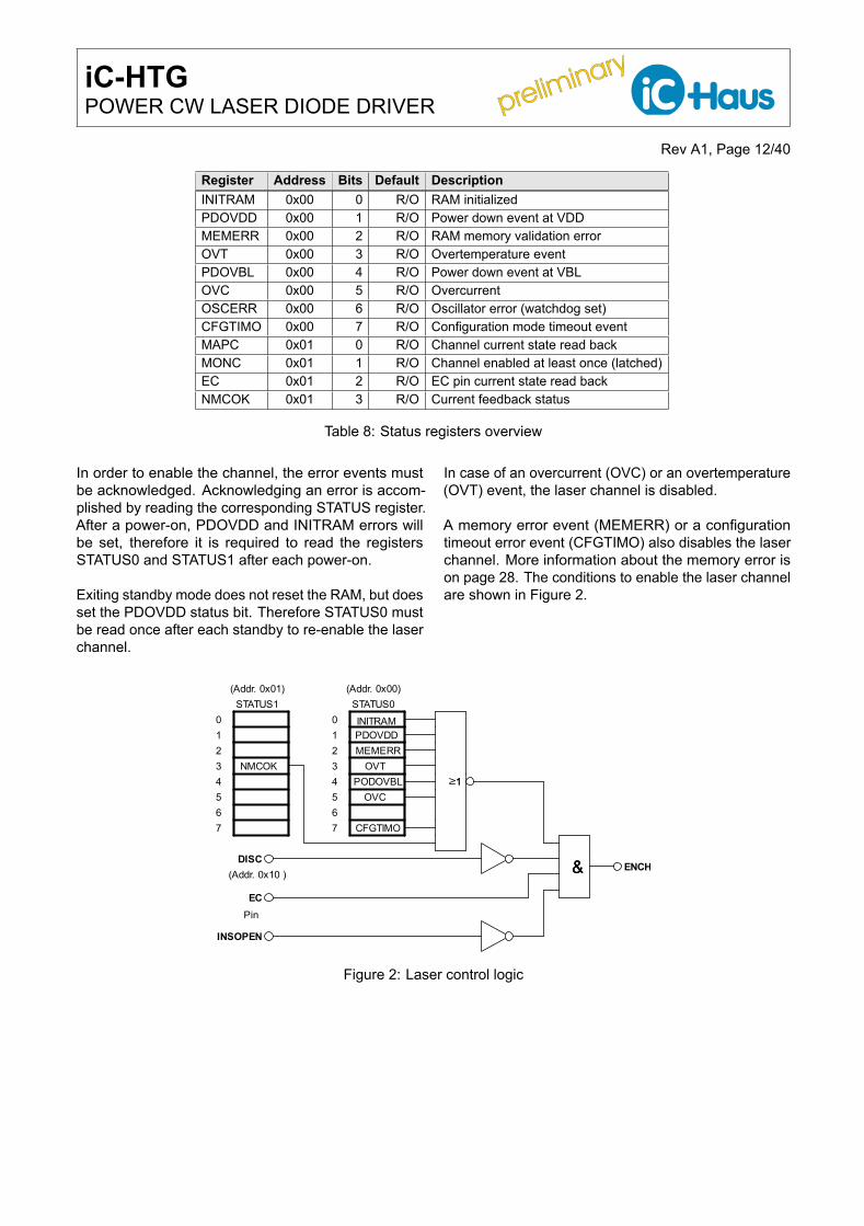
Register Address Bits Default DescriptionINITRAM 0x00 0 R/O RAM initializedPDOVDD 0x00 1 R/O Power down event at VDDMEMERR 0x00 2 R/O RAM memory validation errorOVT 0x00 3 R/O Overtemperature eventPDOVBL 0x00 4 R/O Power down event at VBLOVC 0x00 5 R/O OvercurrentOSCERR 0x00 6 R/O Oscillator error (watchdog set)CFGTIMO 0x00 7 R/O Configuration mode timeout eventMAPC 0x01 0 R/O Channel current state read backMONC 0x01 1 R/O Channel enabled at least once (latched)EC 0x01 2 R/O EC pin current state read backNMCOK 0x01 3 R/O Current feedback status
Table 8: Status registers overview
In order to enable the channel, the error events mustbe acknowledged. Acknowledging an error is accom-plished by reading the corresponding STATUS register.After a power-on, PDOVDD and INITRAM errors willbe set, therefore it is required to read the registersSTATUS0 and STATUS1 after each power-on.
Exiting standby mode does not reset the RAM, but doesset the PDOVDD status bit. Therefore STATUS0 mustbe read once after each standby to re-enable the laserchannel.
In case of an overcurrent (OVC) or an overtemperature(OVT) event, the laser channel is disabled.
A memory error event (MEMERR) or a configurationtimeout error event (CFGTIMO) also disables the laserchannel. More information about the memory error ison page 28. The conditions to enable the laser channelare shown in Figure 2.
(Addr. 0x00)
56
1
(Addr. 0x10 )
Pin
PODOVBL
CFGTIMO
4
PDOVDD0
STATUS0
3
INITRAM
OVT
OVC
2
7
NMCOK
STATUS101234567
MEMERR
(Addr. 0x01)
1
INSOPEN
ENCHDISC
EC
&&
1
Figure 2: Laser control logic
preliminary
preliminary iC-HTGPOWER CW LASER DIODE DRIVER
Rev A1, Page 13/40
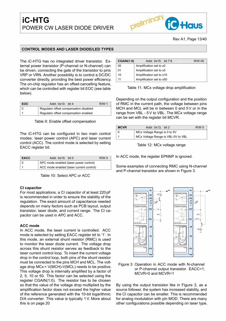
CONTROL MODES AND LASER DIODE/LED TYPES
The iC-HTG has no integrated driver transistor. Ex-ternal power transistor (P-channel or N-channel) canbe driven, connecting the gate of the transistor to pinsVRP or VRN. Another possibility is to control a DC/DCconverter directly, providing the best power efficiency.The on-chip regulator has an offset-cancelling feature,which can be controlled with register bit EOC (see tablebelow).
EOC Addr. 0x10; bit 4 R/W 10 Regulator offset compensation disabled1 Regulator offset compensation enabled
Table 9: Enable offset compensation
The iC-HTG can be configured in two main controlmodes: laser power control (APC) and laser currentcontrol (ACC). The control mode is selected by settingEACC register bit.
EACC Addr. 0x10; bit 0 R/W 00 APC mode enabled (laser power control)1 ACC mode enabled (laser current control)
Table 10: Select APC or ACC
CI capacitorFor most applications, a CI capacitor of at least 220 pFis recommended in order to ensure the stability of theregulation. The exact amount of capacitance neededdepends on many factors such as PCB layout, outputtransistor, laser diode, and current range. The CI ca-pacitor can be used in APC and ACC.
ACC modeIn ACC mode, the laser current is controlled. ACCmode is selected by setting EACC register bit to ’1’. Inthis mode, an external shunt resistor (RMC) is usedto monitor the laser diode current. The voltage dropacross this shunt resistor serves as feedback to thelaser current control loop. To insert the current voltagedrop in the control loop, both pins of the shunt resistormust be connected to the pins MCH and MCL. The volt-age drop MCx = V(MCH)-V(MCL) needs to be positive.This voltage drop is internally amplified by a factor of2, 5, 10 or 50. This factor can be selected using theregister CGAIN(1:0). The resistor has to be chosenso that the value of the voltage drop multiplied by theamplification factor does not exceed the higher valueof the reference generated with the 10-bit logarithmicD/A converter. This value is typically 1 V. More aboutthis is on page 20
CGAIN(1:0) Addr. 0x15; bit 7:6 R/W 0000 Amplification set to x201 Amplification set to x510 Amplification set to x1011 Amplification set to x50
Table 11: MCx voltage drop amplification
Depending on the output configuration and the positionof RMC in the current path, the voltage between pinsMCH and MCL will be in between 0 and 5 V or in therange from VBL - 5 V to VBL. The MCx voltage rangecan be set with the register bit MCVR.
MCVR Addr. 0x13; bit 2 R/W 00 MCx Voltage Range is 0 to 5V1 MCx Voltage Range is VBL-5V to VBL
Table 12: MCx voltage range
In ACC mode, the register EPNNP is ignored.
Some examples of connecting RMC using N-channeland P-channel transistor are shown in Figure 3.
-++
-
CURRENTCHANNELCURRENTCHANNEL
LASERREGULATOR LASERREGULATOR
POWERCHANNELPOWERCHANNEL
x5,x10,x50x5,x10,x50
..VBL-5V
ANIN
RMC
DCO
RMC
MCH
DCO DCODCO
MCH
ANIN
MCL MCL
VRN
VRP
VRN
VRP
8Bit 8Bit
VBL VBLVBLVBL
..5V
255 255
+
CI
+
CI
MDMD
MR
CILCIL
MR
- -CICI CICI
RR+
+
0
+
+
+
+
0
-
-
-
-
-
-
VRN
CI
VBL
DCO
VRN+
DCO
ANIN
MCL
VBL
VRP
MD
MCH
ANIN
MR MR
-
MCL
CIL
MD
MCH
-+VRP
CI
CIL
VBL VBL
Figure 3: Operation in ACC mode with N-channelor P-channel output transistor. EACC=1,MCVR=0 and MCVR=1
By using the output transistor like in Figure 3, as asource follower, the system has increased stability, andthe CI capacitor can be smaller. This is recommendedfor analog modulation with pin MOD. There are manyother configurations possible depending on laser type,

preliminary
preliminary iC-HTGPOWER CW LASER DIODE DRIVER
Rev A1, Page 14/40
transistor, and voltage range. More information aboutthis can be found on page 35.
ACC mode monitoring the optical powerIn ACC mode, the optical power can be measured usinga laser with an integrated photodiode (N-type or P-type).Connecting the photodiode to pin MD, a proportionalvoltage to the photocurrent can be measured with the10-bit linear A/D converter. Two examples of driving inACC mode using a laser with integrated photo diodesare shown in Figure 4. More examples of configurationfor this application can be found on page 35. Depend-ing on the type of laser, N or P, the register bit EPNNPhas to be set to ’0’ or ’1’, respectively.
EPNNP Addr. 0x13; bit 7 R/W 00 N-type laser1 P-type laser
Table 13: Enable P-laser or N-laser type
The optical power can be measured when the photocur-rent is induced in a resistor, producing a voltage dropas shown in Figure 4. The internal 8-bit programmablelogarithmic resistor PLR (more information about thePLR on page 19) can be used. If an external resistoris desired, it must be connected to pins MD and MR,and the internal resistor PLR must be disconnected, bysetting register bit DISP to ’1’.
DISP Addr. 0x10; bit 2 R/W 00 PLR enabled1 PLR disabled
Table 14: Enable/disable PLR
To measure the optical power, the register ADCC(2:0)has to be set to 0b011. Thus, the internal voltageMDL = |VMD − VMR| will be selected as an input for the10-bit A/D converter.
ADCC(2:0) Addr. 0x10; bit 7:5 R/W 000000 ADC sourced by V(VDD) ÷ 8 (3V .. 5.5V)001 ADC sourced by V(VBL) ÷ 30 (3V .. 24V)010 ADC sourced by V(VB) ÷ 30 (3V .. 24V)011 ADC sourced by V(MDL) (0V .. 1.1V)100 ADC sourced by V(MC) (0V .. 1.1V)101 ADC sourced by V(VRN) ÷ 30 (0V .. 24V)110 ADC sourced by V(VRP) ÷ 30 (0V .. 24V)111 ADC sourced by V(ANIN) (0V .. 1.1V)
Table 15: ADC source selection
N
P
-+
-+
CURRENTCHANNELCURRENTCHANNEL
LASERREGULATOR LASERREGULATOR
POWERCHANNELPOWERCHANNEL
x5,x10,x50x5,x10,x50
..VBL-5V
DCO
ANIN
DCO DCO DCO
MCHMCH
RMC RMC
ANIN
VDD
MCL MCL
VRN
VRP
VRN
VRP
8Bit 8Bit
VBLVBL VBLVBL
..5V
255255
CI
++
CI
MD MD
CIL CIL
MR MR
- -CI CICI CI
R
N
P
R
+
0 0
+
+
+
+
+
-
-
-
--
-
VRN
VRP
-
MD
MR
CIL
VBL
MR
VBL
CI
MCH
VBL
CI
DCO
VBL
MD
VRN
CIL
VDD
MCH
ANIN
-
VRP+
DCO
MCL MCL
+
ANIN
Figure 4: Example of ACC monitoring the opticalpower EACC=1. In the left setup MCRV=0and EPNNP=0 while in the right setup,MCVR=1 and EPNNP=1
APC modeIn APC mode, the laser power is controlled. APC modeis selected by setting EACC register bit to ’0’. In thismode, the monitor diode current is used as feedbackin the laser power control loop. To introduce the mon-itor diode current in to the feedback control loop pinsMR and MD are used. An internal, 8-bit programmablelogarithmic monitor resistor (PLR) can be used in APCmode and is controlled by register RMD(7:0). It is alsopossible to use an external monitor resistor connectedto pins MR and MD. If register bit DISP is ’0’, the PLRis present. If DISP is ’1’, the PLR is disabled and an ex-ternal monitor resistor must be used. The PLR featurea wide logarithmic resistor range from 100Ω to 500 kΩ,in steps of typically 3.3%. This covers a wide range ofmonitor currents. More information about the PLR canbe found on page 19.
For fine-tuning the optical power, the reference voltageis set with a 10-bit logarithmic D/A converter, which isconfigurable using register REF(9:0).
REF(9:8) Addr. 0x13; bit 1:0 R/W 0x000REF(7:0) Addr. 0x14; bit 7:0 R/W 0x0000x000 Regulator reference voltage set to minimum voltage. . . Regulator reference voltage set to
Vref = Vref0(1 + ∆ Vref (%)100 )n+1, n from 0 to 1023
0x3FF Regulator reference voltage set to maximum voltage
Table 16: Channel regulator voltage reference
This converter has a voltage range that goes typicallyfrom Vref0=0.1 V to Vrefmax=1.1 V, allowing an opera-

preliminary
preliminary iC-HTGPOWER CW LASER DIODE DRIVER
Rev A1, Page 15/40
tion resolution of typically ∆Vref=0.235%. More infor-mation on the logarithmic D/A converted can be foundon page 20. For calculating the minimum value forthe monitor feedback current (Imon), Vref(0x00, maxvalue) (cf. Electrical Characteristics No. 303) andRmda(RMDx = 0xFF, min value) (cf. Electrical Char-acteristics No. 201) are used.
Imon(min) = Vref (0x000,max)Rmda(RMDx =0xFF,min) = 0.11
350000 = 0.31 uA
To calculate the maximum value of Imon, Vref(0x3FF,min value) (cf. Electrical Characteristics No. 303) andRmda(RMD(7:0) = 0x00, max value) (cf. Electrical Char-acteristics No. 201) are used. The following formula isused to calculate Rmda(RMD(7:0) = 0x00, max value):
Imon(max) = Vref (0x3FF,min)Rmda(RMD=0x00,max) = 1.00
280 = 3.5 mA
Any other Imon value can be calculated using the Rmdformula above. Due to its logarithmic characteristic, thesteps between two consecutive values is kept typicallywithin 3.3 % of the nominal value. This formula provideonly an approximated value of the resistor. Because ofthe coupling factor between laser and photodiode, andthe parametric variation of the PLR, each system hastto be calibrated separately.
P
N+-
+-
CURRENTCHANNELCURRENTCHANNEL
LASERREGULATORLASERREGULATOR
POWERCHANNELPOWERCHANNEL
x5,x10,x50x5,x10,x50
DCO DCO DCO
MCH MCH
DCO
ANINANIN
VDD
MCLMCL
VRP
VRN
VRP
VRN
8Bit 8Bit
VBL VBLVBL VBL
255 255
CI
+ +
CI
MDMD
CIL
MR
CIL
MR
--CICI CICI
P
R
N
R
+ +
0
++
+ +
0
-
-
-
- -
-
MR
MCH
MD
--
MCL
DCO
+
VDD
VBL
+
CI
VRN
ANIN
MR
VBL VBL
MD
DCO
ANIN
VRP
MCH
MCL
VBL
CIL
CI
CIL
VRN
VRP
Figure 5: APC with N-channel and P-channel outputtransistor using N-type and P-type laserdiodes. EACC=0, MCVR=0, EPNNP=0for N-type lasers or EPNNP=1 for P-typelasers.
iC-HTG is optimized for driving P-type and N-type laserdiodes. Figure 5 shows two examples of driving P-typeand N-type laser diodes using APC mode. More exam-ples of possible configurations can be found on page35.
APC mode monitoring the laser current
In APC mode, there is the possibility to monitor the lasercurrent using the 10-bit linear A/D converter and/or touse the overcurrent monitor function. More about over-current on page 16. To measure the optical power, ashunt resistor must be connected to pins MCH/MCLand the register ADCC(2:0) has to be set to 0b100.
ADCC(2:0) Addr. 0x10; bit 7:5 R/W 000000 ADC sourced by V(VDD) ÷ 8 (3V .. 5.5V)001 ADC sourced by V(VBL) ÷ 30 (3V .. 24V)010 ADC sourced by V(VB) ÷ 30 (3V .. 24V)011 ADC sourced by V(MDL) (0V .. 1.1V)100 ADC sourced by V(MC) (0V .. 1.1V)101 ADC sourced by V(VRN) ÷ 30 (0V .. 24V)110 ADC sourced by V(VRP) ÷ 30 (0V .. 24V)111 ADC sourced by V(ANIN) (0V .. 1.1V)
Table 17: ADC source selection
Thus, the internal voltage MC=V(MCH)-V(MCL) will beselected as an input for the 10-bit A/D converter.
N
P
-+
-+
CURRENTCHANNELCURRENTCHANNEL
LASERREGULATOR LASERREGULATOR
POWERCHANNELPOWERCHANNEL
x5,x10,x50x5,x10,x50
..VBL-5V
DCO
ANIN
DCO DCO DCO
MCHMCH
RMC RMC
ANIN
VDD
MCL MCL
VRN
VRP
VRN
VRP
8Bit 8Bit
VBLVBL VBLVBL
..5V
255255
CI
++
CI
MD MD
CIL CIL
MR MR
- -CI CICI CI
R
N
P
R
+
0 0
+
+
+
+
+
-
-
-
--
-
VRN
VRP
-
MD
MR
CIL
VBL
MR
VBL
CI
MCH
VBL
CI
DCO
VBL
MD
VRN
CIL
VDD
MCH
ANIN
-
VRP+
DCO
MCL MCL
+
ANIN
Figure 6: Example of APC monitoring the laser cur-rent. EACC=0. Left setup:MCRV=0,EPNNP=0. Right setup MCVR=1,EPNNP=1
More configuration examples can be found on page 35.
Other functions
For some special applications (for example with lowVB/VBL) it is useful to drive VRN up to VBL. In thiscase, the register bit VRNHR has to be set to ’1’. The

preliminary
preliminary iC-HTGPOWER CW LASER DIODE DRIVER
Rev A1, Page 16/40
default and recommended value is setting the registerbit VRNHR to ’0’.
VRNHR Addr. 0x13; bit 4 R/W 00 VRN set from 0V to VBL-1V1 VRN set from 1V to VBL
Table 18: VRN voltage range
Some applications might need an extra amplificationstage after VRN/VRP with inversion of the polarity of
the control. For such application, the register bit NSW isto be set to ’0’ and the polarity of the controller inverted.
NSW Addr. 0x13; bit 6 R/W 10 Inverted regulation mode (reference connected to
regulator’s negative input)1 Standard regulation mode (reference connected to
regulator’s positive input)
Table 19: CI regulator reference Swap
OVERCURRENT MONITOR
A programmable overcurrent shutdown can be set toprotect the laser by disabling the channel. If the volt-age drop at the external shunt resistor V(MCH)-V(MCL)is higher than the programmed value the overcurrentsignal, OVC, is set and the laser channel is disabled.The maximum voltage drop at the shunt resistor can beprogrammed using the register ILIM(7:0).
ILIM(7:0) Addr. 0x11; bit 7:0 R/W 0x000x00 Overcurrent detection disconnected.0x01 Minimum value of V(MCH)-V(MCL) set to minimum
value typ. (0.1V/CGAIN). . .0xFF Maximum value of V(MCH)-V(MCL) set to maximum
value typ. (1.1V/CGAIN)
Table 20: ILIM overcurrent register
An overcurrent event can be simulated using SOVC.If SOVC = 1, and the overcurrent detection is enabled(ILIM not set to 0x00), the corresponding overcurrenterror bit OVC is set to 1, the error is signaled at NCHK,and the laser channel is disabled. The overcurrent errorwill remain forced until SOVC = 0.
SOVC Addr. 0x16; bit 5 R/W 00 No overcurrent event is simulated.1 Overcurrent event simulated.
Table 21: Simulate overcurrent
WATCHDOG TIMER
The internal 200 kHz oscillator is monitored with theWatchdog Timer (WDT).
If the oscillator remains longer than the maximum timeof tWDT (cf. Electrical Characteristics No. E03) withoutactivity, an oscillator error is triggered. An oscillatorerror sets OSCERR error bit to ’1’. The automatic off-set compensation of the laser control (see page 13)requires the oscillator.
The state of OSCERR is signaled at pin NCHK. Thesignaling of OSCERR state can be masked with bitMOSCERR. Setting MOSCERR to ’1’ masks the oscil-lator error and in this case OSCERR is not signaled atNCHK.
It is possible to simulate an error of the oscillator usingSOSCERR bit. If SOSCERR = 1, the oscillator error isforced. When OSCERR is set to ’1’, the error is signaledthrough NCHK depending on the state of MOSCERR.
OSCERR Addr. 0x00; bit 6 R0 Oscillator functioning OK1 Watchdog timeout set on oscillator failure.
Cleared on read
Table 22: Oscillator watchdog
MOSCERR Addr. 0x16; bit 0 R/W 00 Oscillator error (watchdog) will be signaled at NCHK1 Oscillator error (watchdog) will not be signaled at
NCHK
Table 23: Oscillator watchdog error mask
SOSCERR Addr. 0x16; bit 7 R/W 00 No oscillator error simulated.1 Oscillator error simulated (watchdog timeout).
Table 24: Simulate oscillator error

preliminary
preliminary iC-HTGPOWER CW LASER DIODE DRIVER
Rev A1, Page 17/40
SERIAL COMMUNICATION INTERFACES
Communication modesiC-HTG can be configured via a serial interface. It hastwo communication modes: SPI and I2C. Selection ofthe communication protocol is achieved using pin INS:INS = hi for I2C, INS = lo for SPI. If the pin INS is foundto be open, NCHK will be pulled to 0.
SPI slave interfaceThe SPI slave interface is enabled by setting pin INSto lo and the interface uses pins NCS/A1, SCLK/SCL,MISO/SDA and MOSI/A0. The pin NCS/A1 is the chipselect pin and must be set lo by the SPI master in or-der to start communication. The pins MISO/SDA andMOSI/A0 are the data communication lines and pinSCLK/SCL is the clock line generated by the SPI mas-
ter (e.g. a microcontroller). The SPI protocol framesare shown in Figure 7.
A communication frame consists of one address byteand at least one data byte. The bits 7:6 of the addressbyte are the opcode used for selecting a read opera-tion (set to "10") or a write (set to "01") operation. Theremaining 6 bits are used for register addressing.
It is possible to transmit several bytes consecutivelyif the NCS signal is not reset and SCLK/SCL keepsclocking, as is shown in Figure 7. The address is in-ternally incremented after each transmitted byte. Oncethe address reaches the last register (0x3F), it is resetback to 0x00.
13 14 15
MOSI
SPI READ COMMAND FRAME. OPCODE = 10, POLARITY = 0, PHASE = 0
SPI WRITE COMMAND FRAME. OPCODE = 01, POLARITY = 0, PHASE = 0
NCS
Don't care
16 17
Data n HIZMISO HIZ (Pull-Up) Don't care Data 1 MSB first Data 2
Init Addr.(5:0) MSB first
SCLK 0 1 2 3 4 5 6 7 8 9 10 11 12 13 14 15
MOSI
0 1SCLK
Data 1 MSB first Data 2
16 17
Data n Don't care
MISO HIZ (Pull-Up) Don't care
NCS
2
Init Addr.(5:0) MSB first
3 4 5 6 7 8 9 10 11 12
Figure 7: SPI commands
I2C slave interfaceThe I2C slave interface is enabled by setting pin INSto hi and the interface uses pins NCS/A1, SCLK/SCL,MISO/SDA, ID, and MOSI/A0. The protocol frames areshown in Figure 8.
A communication frame consists of one slave addressbyte, one register address byte, and at least one databyte. The bits 7:1 of the slave address byte are buildform the slave identification code (ID) and the addressbit A1 and A0. The bit 0 is used to specify the datadirection (RNW: 1 for read, 0 for write).
The four most significant bits are fixed by default to thevalue 0b1010. The pins MOSI/A0, NCS/A1, and ID areused to set the remaining slave ID bits (see Tables 25and 26).
Action b7 b6 b5 b4 b3 b2 b1 b0Write to slave 1 0 1 0 ID A1 A0 0Read from slave 1 0 1 0 ID A1 A0 1
Table 25: I2C write/read byte

preliminary
preliminary iC-HTGPOWER CW LASER DIODE DRIVER
Rev A1, Page 18/40
Action ID A1 A0 Slave ID Command byteWrite to slave 0 lo lo lo 0x50 0xA0Read from slave 0 lo lo lo 0x50 0xA1Write to slave 1 lo lo hi 0x51 0xA2Read from slave 1 lo lo hi 0x51 0xA3Write to slave 2 lo hi lo 0x52 0xA4Read from slave 2 lo hi lo 0x52 0xA5Write to slave 3 lo hi hi 0x53 0xA6Read from slave 3 lo hi hi 0x53 0xA7Write to slave 4 hi lo lo 0x54 0xA8Read from slave 4 hi lo lo 0x54 0xA9Write to slave 5 hi lo hi 0x55 0xAARead from slave 5 hi lo hi 0x55 0xABWrite to slave 6 hi hi lo 0x56 0xACRead from slave 6 hi hi lo 0x56 0xADWrite to slave 7 hi hi hi 0x57 0xAERead from slave 7 hi hi hi 0x57 0xAF
Table 26: I2C write/read command byte
7 8
8 9
2
A1:A0
3 4
Addr.MSBfirst
Start
SDA
7
SlaveACK
21
Data1 Data2
1
SlaveACK
Data1
7 8
MasterACK
9 1
Data2
2
Stop
Datan
A1:A0
0 4 5 6 8
9
9 1
8
A1:A0
SlaveACKRNW='0'
9
SlaveACK
9
Stop
Data1
1
.
SCL 0 1 2 3
RNW='0' RepeatedStart
0
Datan
7 8 9
SlaveACK
4 5 6 7
6 7
1 2
RNW='1'
Data1
5 6
7 8 9
1
SlaveACK
7 8
.
8
I2CREADCOMMANDFRAME.
1
Addr.MSBfirst
Start
SCL 2
SlaveACK
I2CWRITECOMMANDFRAME.
3 3 4 5 6
SDA
7
Figure 8: I2C commands

preliminary
preliminary iC-HTGPOWER CW LASER DIODE DRIVER
Rev A1, Page 19/40
8-BIT INTERNAL PROGRAMMABLE LOGARITHMIC MONITOR RESISTORS
An internal 8-bit Programmable Logarithmic monitorResistor (PLR) is provided for the APC.
The PLR is used to control the optical power of thelaser diode in APC mode or to measure a monitor pho-tocurrent in ACC mode using the internal A/D converter.The resistor is connected to pins MR and MD usinga Force Sense switch structure. This ensures a lowthermal dependence, and a monotone dependence onthe resistor with the register value RMD(7:0). Note thatmeasuring of the internal resistor directly at externalpins MD-MR is not possible (see Figure 9).
-+
4BitsRes.Decoder
POWERCHANNELEPNNP
DCODCO
+
MD
MR
-
0 1 EPNNP MR
+-
DCO
MD
Figure 9: PLR internal node regulation
The internal resistor value can be selected from 256 val-ues, ranging from typ. Rmd0=100Ω to over 500 kΩ, fol-lowing logarithmic increments with a typical step widthof ∆Rmd=3.3%. The resistors are configured with reg-ister RMD(7:0).
RMD(7:0) Addr. 0x12; bit 7:0 R/W 0xFF0x00 PLR set to the minimum resistance. . . PLR set to
Rmd = Rmd0(1 + ∆ Rmd(%)100 )n+1, n from 0 to 255
0xFF PLR resistor set to the maximum resistance
Table 27: MR-MD resistance selection
The following formula calculates the register RMD(7:0)in order to set the desired resistor value:
Rmd = Rmd0(1 + ∆ Rmd(%)100 )n+1, : n ∈ [0, 255],
where Rmd0 is the minimum resistor value (typically100Ω), ∆Rmd(%) is the step between two consecutiveresistor values (typically 3.3%) and n is the value ofRMD(7:0) register in decimal.
Since the PLR has parametric variations and covers awide range of resistors values, the given formula is onlyfor simulation or information purposes. Each systemhas to be calibrated separately. The recommendedprocedure is to enable the channel with a high valueof RMD(7:0) and a medium value on register REF(9:0).While measuring the optical power reduce the PLRvalue until the desired optical power is reached. Thenusing the register REF(9:0) you can make a more accu-rate selection of the optical power. For more informationsee 13.
The PLR is disabled by using the register bit DISP.
DISP Addr. 0x10; bit 2 R/W 00 PLR enabled1 PLR disabled
Table 28: Enable/disable PLR
In ACC mode the PLR is not used in the control circuit.Even though the PLR is not in the control circuit, it canbe enabled (DISP = 0) in order to give feedback usingthe 10-bit A/D converter to control the light power if amonitor diode is connected.
Alternatively, an external monitor resistor can be usedto measure the optical power, which requires DISP tobe set to ’1’.

preliminary
preliminary iC-HTGPOWER CW LASER DIODE DRIVER
Rev A1, Page 20/40
10-BIT LOGARITHMIC D/A CONVERTER
The 10-bit logarithmic D/A converter is used for settingthe regulator’s voltage reference. The D/A converteris active in all operating modes. With a range from 0.1to 1.1 V and the typical step width is ∆Vref=0.235%.(Maximal ∆Vref=1%) This ensures that with each LSBstep there is a maximum variation of 1% of the opticalpower.
The D/A converter is configured using register REF(9:0).With REF(9:0) = 0x000, the D/A output value is set to0.1 V, and for REF(9:0) = 0x3FF the D/A output is con-figured to 1.1 V.
REF(9:8) Addr. 0x13; bit 1:0 R/W 0x000REF(7:0) Addr. 0x14; bit 7:0 R/W 0x0000x000 Regulator reference voltage set to minimum voltage. . . Regulator reference voltage set to
Vref = Vref0(1 + ∆ Vref (%)100 )n+1, n from 0 to 1023
0x3FF Regulator reference voltage set to maximum voltage
Table 29: Channel regulator voltage reference
To calculate the D/A converter value for each REF(9:0)value, use the following equation:
Vref = Vref0(1 + ∆ Vref(%)100 )n+1 : n ∈ [0, 1023],
where Vref0 is the minimum value (typically 0.1 V),∆Vref (%) is the step value (typically 0.235 %) and n isthe value of REF register in decimal.
Since the D/A has parametric variations, the given for-mula is only for simulation or information purposes.Each system has to be calibrated separately. The rec-ommended procedure in APC mode is to enable thechannel with a high value of RMD(7:0) and a mediumvalue on register REF(9:0). While measuring the opticalpower, reduce the PLR value until the desired opticalpower is reached. Then using the register REF(9:0)you can make a more accurate selection of the opticalpower. For ACC mode is recommended to enable thelaser with register value REF(9:0)=0xFF. While measur-ing the optical power, reduce the value of the registerREF(9:0) until reaching the desired optical power. Formore information see 13.

preliminary
preliminary iC-HTGPOWER CW LASER DIODE DRIVER
Rev A1, Page 21/40
10-BIT LINEAR A/D CONVERTER
A 10-bit linear A/D converter is available for a varietyof voltages that can be measured with different resolu-tions:
• V(VDD) up to 5.5 V with 8.6 mV resolution• V(VBL) up to 30 V with 32.3 mV resolution• V(VB) up to 30 V with 32.3 mV resolution• V(MDL) internal voltage up to 1.1 V with 1.075 mV
resolution• V(MC) internal voltage up to 1.1 V with 1.075 mV res-
olution• V(VRN) up to 30 V with 32.3 mV resolution• V(VRP) up to 30 V with 32.3 mV resolution• V(ANIN) up to 1.1 V with 1.075 mV resolution
As described in block diagram on Page 1, the voltagesV(VDD), V(VBL), V(VB), V(VRN), V(VRP) and V(ANIN)are th PIN Voltage directly. V(MC) is proportional tothe laser current value and is the voltage difference be-tween pins MCH and MCL. (V(MC)=V(MCH)-V(MCL)).The voltage V(MDL) is proportional to the optical laserpower (monitor current) and the value is the absolutevalue of the difference between the pins MD and MR(V(MDL)=|V(MD)-V(MR)|).
The register ADCC(2:0) select the signal measured withthe 10-bit A/D converter.
ADCC(2:0) Addr. 0x10; bit 7:5 R/W 000000 ADC sourced by V(VDD) ÷ 8 (3V .. 5.5V)001 ADC sourced by V(VBL) ÷ 30 (3V .. 24V)010 ADC sourced by V(VB) ÷ 30 (3V .. 24V)011 ADC sourced by V(MDL) (0V .. 1.1V)100 ADC sourced by V(MC) (0V .. 1.1V)101 ADC sourced by V(VRN) ÷ 30 (0V .. 24V)110 ADC sourced by V(VRP) ÷ 30 (0V .. 24V)111 ADC sourced by V(ANIN) (0V .. 1.1V)
Table 30: ADC source selection
When enabled, the A/D converter continuously acquiresthe signal selected by ADCC register. The conversiontime is 140µs. Changing the source requires 500µssettling time.
The converter does not provide an end of conversion(EOC) bit, the ADC(9:0) register always contains thevalue of the last valid conversion.
As the A/D converter has a resolution of 10 bits, theresults are split into two, one byte wide, separate reg-isters; ADCh contains ADC MSBs values while ADClstores the LSBs. A consecutive read of both registers(lower and upper part) should be carried out in orderto prevent an undesired change in the measured valuebetween two read commands.
ADC(9:8) Addr. 0x03; bit 1:0 RADC(7:0) Addr. 0x04; bit 7:0 R0x000 ADC minimum value...0x3FF ADC maximum value
Table 31: ADC
The voltage corresponding to the measured digitalvalue can be directly obtained using the following for-mula:
V(VBL, VB, VRP, VRN) = 30 ∗ VFS1024 ∗ ADCx
V(VDD) = 8 ∗ VFS1024 ∗ ADCx
V(MDL, MC, ANIN) = VFS1024 ∗ ADCx
VFS is the full scale voltage of the A/D converter (cf.Electrical Characteristics No. 706) typically 1.1 V. Fora more precise measurement, the A/D converter canbe calibrated by measuring a known VB voltage andcalculating the VFS.

preliminary
preliminary iC-HTGPOWER CW LASER DIODE DRIVER
Rev A1, Page 22/40
ANIN GENERAL PURPOSE IO PIN
The Pin ANIN is a general purpose IO-Pin. Figure 10describe the functionality of pin ANIN.
10BitADC
ADCC(2:0)
DIgitalIO
ADC(9:0)10Bit
VRN/30VRP/30
ANIN
VBL/30
ANINO
RANIN
VDD/8
VB/30
ANIN
MDLMC
DA
7
0
ANIN
VRP/30
VB/30
RANIN
MDL
ANINO
MC
VBL/30
VRN/30
ANIN
ADC(9:0)
VDD/8
Figure 10: ANIN pin function description
With the pin ANIN an external analog Voltage from 0Vto 1.1V can be digitalized using the 10 bit linear A/Dconverter. To this end, register bit ANINO has to be set
to 1 and the register ADCC(2:0) has to be set to value0x07. For the digitalisation of higher voltages a resistordivider is recommended. An example of measuringvoltages up to 24V is shown in figure 13.
ANIN can be used as a digital open collector output. Asdigital output an external Pull-Up resistor needs to beused. The maximum allowed voltage at pin ANIN is 5V.With register bit ANINO the state of ANIN will be set.
ANINO Addr. 0x1C; bit 2 R/W 10 ANIN pin pulled low (open collector)1 ANIN pin set to high impedance
Table 32: ANIN output state
RANIN Addr. 0x01; bit 4 R0 ANIN pin is digital low at the precise reading
moment.1 ANIN pin is digital high at the precise reading
moment.
Table 33: ANIN pin state
As digital TTL input the Pin ANIN is mapped to statusRegister Bit RANIN.

preliminary
preliminary iC-HTGPOWER CW LASER DIODE DRIVER
Rev A1, Page 23/40
DC/DC CONVERTER OPTIMIZATION
iC-HTG provides a 6-bit configurable current source atpin DCO that can be used to trim the output voltage of aDC/DC converter. Current at DCO can be programmedwith register RDCO(5:0). Possible application benefitswith using DCO include:
• DC/DC step down operation: regulation at voltageslower than power supply
• DC/DC step up operation: regulation at voltageshigher than power supply
• Efficiency enhancement
RDCO(5:0) Addr. 0x15; bit 5:0 R/W 0x000x00 No current. . .0x3F 130µA Typ (see spec point D01)
Table 34: DCO current control
The proposed applications can be demonstrated with astandard DC/DC converter, e.g. TPS63060DSC fromTexas Instruments. This converter allows an input volt-age ranging from 2.5 V to 12 V and offers an outputvoltage from 2.5 V to 8 V. It is capable of delivering upto 2 A current, depending on the output voltage. Figure11 shows a possible configuration.
TPS63060
PS/SYNC
2x10uF3x22uF
1uH
L1
PGND
1MEG
VAUX
VOUT VOUT
0.1uF
GND
1uH
C2 C1
C3
VIN VIN
PG
EN
C3
C1
FB
C2R1R3
R2
L1
L1L2
PG
VAUX
VOUT
PS/SYNC
PGND
L2
GND
VIN
FB
VOUT VIN
L1
EN
Figure 11: TPS63060 DC/DC converter from TI
DC/DC step down operation:regulation at voltages lower than power supplyThe resistors R1 and R2 in the feedback path allowsetting the desired output value Vout. The DC/DC con-verter drives Vout pin in order to yield 0.5 V at feed-back pin FB. The DCO output signal from iC-HTG isconnected to FB pin. The Vout is controlled with theinternal register RDCO(5:0) from iC-HTG.
The DCO current into FB node controls the voltages ofthe divider R1 and R2, and Vout changes in order tomaintain 0.5 V at the pin FB. When selecting R1 andR2, one needs to consider:
• Resistors values:R1 = R2( Vout
Vfb − 1)• The current of the voltage divider should be high
enough in comparison to the current from the pin DCOto offer acceptable resolution. The programmable cur-rent resolution of register RDCO(5:0) is 2µA.
• The DCO current into the voltage divider lowers thevoltage Vout. Vout is 8 V when no current is presentat DCO.
Choosing R1 = 100 kΩ, the value of R2 can be calcu-lated:
R2 = R1VoutVfb −1 = 100k
8V0.5V −1 = 6.7 kΩ
With this configuration, the current through the volt-age divider is 75µA at 8 V . The resolution of eachRDCO(5:0) step is then 200 mV.
The value in RDCO(5:0) register needed in order tohave the desired output voltage can be calculated us-ing the following formula:
RDCO = Idco2uA = IR2−IR1
2uA =0.5V6.7k −
Vout−0.5V100k
2uA
+-
CURRENTCHANNEL
LASERREGULATOR
POWERCHANNEL
x5,x10,x50
TPS63060
PS/SYNC
2x10uF3x22uF
1uH
L1
PGND
1MEG
VAUX
VOUT
0.1uF
DCO
MCH
100k
DCO
RMC
ANIN
GND
MCL
VRP
VRN
6.7K
...5V
8Bit
VBL
1uH
255
+
CI
C1
C3
C2
VINVIN
MD
MR
CIL
PG
VB
EN
-
C1C2
FB
C3
R1
R2
R3
3V6V
L2 L1
L1
J1
CICI
R
1
0
+
+
+
32
-
-
-
PG
EN
MR
GND
VIN
CIL
MCL
VRN
VBL
L1
MD
DCO
+
PS/SYNCCI
VAUX
L2
VOUT
VB
ANIN
FB
PGND
MCH
VRP
VIN
-
Figure 12: Regulation of VB / VBL Supply usingDCO
The resulting value varies slightly depending on the tol-erances of the selected resistors and the DCO current.iC-HTG incorporates an internal 10-bit A/D converter.

preliminary
preliminary iC-HTGPOWER CW LASER DIODE DRIVER
Rev A1, Page 24/40
Selecting VBL or VB as input of this converter the sup-ply voltage can be measured and the selected currentat DCO can be changed in order to obtain the desiredvoltage at VBL/VB. Setting register ADCC(2:0) to 0b001or 0b010, the supply voltages VBL or VB can be mea-sured, respectively. The digitalized value is the supplyvalue divided by 30.
DC/DC step up operation: regulation at voltageshigher than power supply
A practical application of the present case is the controlof blue lasers. This type of laser presents a forwardvoltage around 5 V, which demands a voltage of about6 V for the anode of the laser diode (LDA). If the systemis supplied with a 3 V LiPo battery, it is necessary to usea DC/DC in order to step up and drive the laser diodeand driver with a sufficient voltage. Figure 12 showsthis application. Jumper J1 can be set to 1-2 or 2-3position.
Typically setting register RDCO(5:0) to 10 it delivers20µA and 6 V, which are obtained at Vout.
Extension of system working voltage rangeiC-HTG may be supplied with a voltage within thethreshold values of 3 V and 24 V. It is possible to controlthe DC/DC output in a voltage range of 2.5 to 24 V if theDC/DC converter controlled by the DCO output signalis included in the system, as it is shown in Figure 12.
In Figure 12 both the laser and iC-HTG are suppliedwith output voltage Vout from DC/DC converter. Typi-cally, the register RDCO(5:0) is set to 23, which forces48µA to be output to the voltage divider. A systemvoltage of 3.3 V is obtained at Vout.
Efficiency enhancementIf iC-HTG and the laser diode are supplied with thesame power supply, the efficiency of the driver can beimproved depending on the supplied voltage, the sat-uration voltage, and the laser diode forward voltage.The power dissipation of the driver transistor can bereduced if VBL is set through the DC/DC converter con-figured to deliver a voltage lower than the power supplyas shown in Figure 13.
+-
CURRENTCHANNEL
LASERREGULATOR
POWERCHANNEL
x5,x10,x50
TPS63060
PS/SYNC
2x10uF3x22uF
1uH
L1
PGND
1MEG
VAUX
VOUT
0.1uF
ANIN
RMC
460k
DCO
MCH
100k
DCO
GND
MCL
VRP
6.7K
VRN
...5V
8Bit
RA1
VBL
RA215K
1uH
255
C1
+C2
C3
CI
VINVIN
MD
MR
CIL
PG
VB
EN
-
C1
FBC3
C2R1
R3
R2
L1L2
L1
J1
CICI
R
+
+
+
1
0
32
-
-
-
L2
EN
VIN
ANIN
VAUX
VIN
DCO
GND
MD
VOUT
PG+VRN-
MR
FB
CIL
VBL
MCH
L1
MCL
VRP
PS/SYNCCI
VB
PGND
Figure 13: System efficiency enhancement
For this application the pin ANIN must be configured asan input by setting the register bit ANINO to 1. Usingthe resistors RA1 and RA2, the drain voltage at thedrive transistor is reduced by a factor of approximately30. For more information about ANIN see page 22.
ANINO Addr. 0x1C; bit 2 R/W 10 ANIN pin pulled low (open collector)1 ANIN pin set to high impedance
Table 35: ANIN output state
In this configuration, the voltage drop at the driver tran-sistor can be measured and minimized by setting anappropriate supply at VBL. Some steps have to be doneto optimize the power dissipation:
• A. Measure the voltage at pin VBL, setting the registerADCC(2:0) to 0b001. The measured voltage AD(VBL)is divided by a factor of 30.
• B. Measure the voltage at pin ANIN. AD(ANIN)
• C. The voltage drop at the driver transistor is(AD(VBL)-AD(ANIN))*30. By changing the DCO(6:0)register, the supply voltage at V(VBL) can be in-creased or decreased. ANIN should remain constant.
• D. Repeat steps A to C to achieve the desired voltagedrop at the output transistor.

preliminary
preliminary iC-HTGPOWER CW LASER DIODE DRIVER
Rev A1, Page 25/40
ANALOG MODULATION
iC-HTG allows analog modulation of the output currentat a frequency of up to 50 kHz. An external modula-tion voltage source (sinusoidal, triangular, etc) mustbe provided and connected to pin MOD. The internalcontrol loop forces the laser diode current to follow themodulation voltage signal. This feature is enabled bysetting register bit ENAM high.
ENAM Addr. 0x13; bit 3 R/W 00 Analog modulation disabled1 Analog modulation enabled
Table 36: Enable analog modulation
-+
CURRENTCHANNEL
LASERREGULATOR
x2,x5,x10,x50
MODULATION
VMODhigh
VOLTAGEVMODlow
SOURCE
Vmax,r
VMOD
MCVR
VRMC
EACC
Vmin,r
CVBL
10Bit
10Bit
..1.1V
VRN/30VRP/30
MOD
MCH
RMC
VBL/30
MDL
VCU
MCL
VRP
VRN
REF
VDD/8
ENAM
VBLVBL
VB/30
VREF
+
CI
CVBL
MC
ANIN
CIL
MDL
-
MC
CI CID
D
A
A+
0
+
71
0
0
1
-
-t
t
MCL
VRP/30
MCH
CIL
VRN
VBL
VBL/30
VCU
ENAM
MOD
EACC
MDL
VBL
MDL MCVR
MC
VREF
ANIN
VRP
VDD/8
MC
VRN/30
VB/30
CI
+-
Figure 14: Recommended configuration for analogmodulation using N-channel transistor.EACC=1, MCVR=0
+-
CURRENTCHANNEL
LASERREGULATOR
x2,x5,x10,x50
MODULATION
VMODhigh
VOLTAGEVMODlow
SOURCE
Vmax,r
VMOD
VRMC
MCVR
EACC
Vmin,r
CVBL
10Bit
10Bit
VRP/30VRN/30
..24VMOD
RMC
MCH
VBL/30MCL
MDL
Rpull
VCU
VRN
VRPREF
VDD/8
ENAM
VBLVBL
VB/30
VREF 10k+
CVBL
CI
MC
ANIN
CIL
MDL
-
MC
CICID
D
A
A
+
+
7
0
10
10
-
-
t
t
-
VRP/30
VBL
MC
MCVR
CI
MCH
VCU
MCL
VDD/8
ENAM
MDL
VBL/30
VRN+
MDLVB/30
MOD
VRN/30
VREF
CIL
MC
ANIN
VBL
VRP
EACC
Figure 15: Recommended configuration for analogmodulation using P-channel transistor.EACC=1, MCVR=1
The maximum allowed modulation frequency is 50 kHz,but general performance depends on the external ca-pacitor connected at CI, the value of the RMC, the
current gain selected (CGAIN(1:0)), and the total gatecapacity of the external transistor.
To ensure a higher stability, the configuration shownin Figure 15 is recommended (See Figure 19 left fromExamples of configuration on page 35). CGAIN(1:0)must be kept as low as possible, increasing the valueof the RMC if necessary. For 50 kHz modulation figure15 is recommended with values of CI from 100pF to300pF.
Setting Current Modulation
The modulation current is set by 4 factors:
• The modulation voltage amplitude at MOD.• The digital-to-analog converter setpoint REF(9:0)• The external sense resistor RMC.• Current Channel gain CGAIN(1:0).
With the analog modulation VREF is no more a DCvoltage for the regulator but a voltage divider for theV(MOD) voltage to downscale AC and DC voltages forthe regulator. The V(MOD) voltage contains a DC volt-age part and a AC voltage part to define the requiredoperation point with the parameter set.
-+
x2,x5,x10,x50
GAIN(1:0)
REF(9:0)
V(MOD)
V(RMC)
V(REF)
MOD
MCH
RMCMCL
VRN
VBLVBL
3FF
+
VN
-0
x
GAIN(1:0)VN
MCH
VBL VBL
MCL
-+
REF(9:0)
VRN
MOD
Figure 16: Signal path of the analog modulation
It is not recommended to use lower values that 100mVfor V(VREF). For lower voltages the accuracy of the reg-ulation and the frequency response are not guaranteed.Therefore, V(MOD) must be selected according to theREF(9:0) dividing factor to ensure V(VREF) higher orequal to 0.1 V.
For a first estimate of the values, the equation (1) and(2) can be used. In this equation REFx can be 1 to1023 and CGAINx can take the values 2, 5, 10 and 50.

preliminary
preliminary iC-HTGPOWER CW LASER DIODE DRIVER
Rev A1, Page 26/40
(1) V(RMC) = VMOD1023 · REFx
CGAINx
(2) I(RMC) = VMOD1023 · REFx
CGAINx · 1RMC
With this equation the theoretical current value can becalculated. More accurate calculations can be madeusing the parameters 302 303 and 304 of the ElectricalCharacteristics and the equation (3) and (4)
(3) V(RMC) = VMOD1.1 · V(REF)
G()
(4) I(RMC) = VMOD1.1 · V(REF)
G() · 1RMC
Due to the parameter variation is recommended to cali-brate each circuit. The recommended procedure to setthe current modulation values is:
1. Set the GAINx(1:0) value. (0x00 is recom-mended)
2. Set a reference value of voltage in V(MOD). Forexample a low voltage or a DC voltage (VMODdc)in a sinus signal as shown in figure 17
3. With fixed voltage at V(MOD) (for exampleVMODdc), use REF(9:0) to set the desiredV(RMC) (In this case V(RMCdc) for current laser(I(RMCdc)). You can use the internal AD-Con-verter to sense the voltage at RMC.Note that using the equation the laser currentI(RMCdc) is:(5) I(RMCdc) = VMODdc
1.1 · V(REF)G() · 1
RMC
4. With this setup the relationship between the volt-age at V(MOD) and the referenced current isgiven by (7):
(6) I(RMChigh) = VMODhigh1.1 · V(REF)
G() · 1RMC
(7) I(RMChigh)I(RMCdc) = VMODhigh
VMODdc
VMODhigh
VRMChigh
VMODlow
VRMClow
VMODdc
VRMCdc
VMOD
VRMC
VMac
VMdc
VRac
VRdc
t
t
Figure 17: Example of modulation voltages

preliminary
preliminary iC-HTGPOWER CW LASER DIODE DRIVER
Rev A1, Page 27/40
TEMPERATURE MONITOR AND PROTECTION
iC-HTG includes an 8-bit temperature monitor that al-lows to measure the internal chip temperature goingfrom -40 to 125 °C. The resolution is 1 °C/LSB.
TEMP(7:0) Addr. 0x02; bit 7:0 R0x00 Minimum temperature. . .0xFF Maximum temperature
Table 37: Chip temperature
Absolute read values may differ from one chip to an-other. An individual initial calibration of the temperaturemonitor is recommended. The TEMP register mustbe read at a known temperature. Using the resolu-tion value of 1 °C/LSB, the internal temperature can becalculated.
The temperature monitor can be used to compensatetemperature effects on the laser diode. The microcon-troller can use a laser diode characteristic formula ora look-up table combined with the temperature valuemeasured using TEMP register. The reference voltagecan be configured accordingly in order to compensatefor temperature effects.
iC-HTG is protected against overtemperature. If the in-ternal temperature exceeds a safety value, an overtem-perature error bit (OVT) is set to 1. If OVT = 1, the laserchannel is disabled, and the error event is signaledthrough NCHK pin. The error bit OVT is latched, andcan only be cleared by reading the status register.
The overtemperature threshold value can not be config-ured.
OVT Addr. 0x00; bit 3 R0 No overtemperature event has occurred since last
read1 Overtemperature event has occurred. Cleared on
read
Table 38: Overtemperature
It is possible to simulate an overtemperature event us-ing the SOVT bit. Setting SOVT to 1, the overtempera-ture error flag OVT is set to 1. iC-HTG remains in theerror state until SOVT is set back to 0.
SOVT Addr. 0x16; bit 4 R/W 00 No overtemperature event is simulated.1 Overtemperature event simulated.
Table 39: Simulate overtemperature

preliminary
preliminary iC-HTGPOWER CW LASER DIODE DRIVER
Rev A1, Page 28/40
CONFIGURATION MODE AND MEMORY INTEGRITY MONITOR
iC-HTG supports the interfaces SPI or I2C, which areselected by the INS pin. More information about theserial communication interface can be found on page17
In the configuration mode the iC-HTG configuration canamended without affecting the configuration stored inthe iC-HTG RAM. Only when switching back to the op-eration mode, the configuration is applied to the iC-HTGin an atomic operation (all at once).
Integrity monitoring is implemented by a duplication ofthe configuration registers into a validation page (seedescription below) where the registers are automati-cally copied with their inverted value. Every registerbit is compared with its validation copy and, in case ofinconsistency, a memory error is generated in such acase the laser channel is switched off.
Atomic appliance is achieved by latching the configura-tion registers. This permits a full configuration (differentregisters) to be made prior to apply it to the laser chan-nel.
The configuration mode is selected by setting the regis-ter MODE(1:0) to 10.
MODE(1:0) Addr. 0x1C; bit 1:0 R/W 0100 Not allowed, signaled as memory error01 Chip set in operation mode
(apply configuration, latch transparent)10 Chip set in configuration mode
(hold previous configuration)11 Not allowed, signaled as memory error
Table 40: Select configuration or operation mode
In Configuration mode, the configuration memory(addr. 0x10 to 0x1F) can be written and read backto check a correct communication without changing thepresent configured operation state of the iC-HTG. Inthis mode, the memory integrity check is disabled.
iC-HTG will monitor the time elapsed in configurationmode and automatically switch the laser off if it exceedsa configuration mode timeout. The time in configura-tion mode must be less than 40 ms to ensure that noconfiguration timeout occurs during configuration (cf.Electrical Characteristics No. E02).
When writing the configuration is completed, iC-HTGis switched to operation mode by writing "01" into theMODE register (addr. 0x1C). In operation mode theconfiguration is applied to the iC-HTG and the memoryintegrity check activated. In this mode configurationregisters can only be read (except MODE(1:0) regis-ter, which is always accessible). Figure 18 shows theinterface to the memory structure.
RNW
RNW_RAM
MEMERR
LATCH
CFG(127:0)
CHECKERROR
DB(7:0)
RAM
Addr. Decoder
RNW_VAL
VALIDATION
SPI / I2C
Addr. 0x1C
0x10
0x1F
MODE
0x30
0x3F
ADR(6:0)
&&
Figure 18: Interface, RAM integrity monitoring, and configuration latching
Register map descriptionThe register map consists of 64 addresses subdividedin three different pages:
• Read-only page, addr. 0x00 to 0x0F: iC-HTG sta-tus, ADC readout, thermometer readout and chiprevision.

preliminary
preliminary iC-HTGPOWER CW LASER DIODE DRIVER
Rev A1, Page 29/40
• Configuration page (integrity monitored), read--write registers, addr. 0x10 to 0x1F.
• Validation page, read-write registers, addr. 0x30to 0x3F.
Read-only registers with values or statesThe Read-only registers are sub-divided into status reg-isters (addr. 0x00 to 0x01) and measurement registersand the chip revision register CHIPREV. Status regis-ters are normally latched to 1 on events and cleared onread (see individual register description). Measurementregisters are dual-port and can be accessed simultane-ously with the measurements in progress. ADC (addr.0x03 to 0x04) is a 10-bit register split into two 8-bitregisters and must be accessed in block mode (auto-matic address increment) to ensure data do not changeduring the read.
Configuration page (integrity monitored)The configuration page (addr. 0x10 to 0x1F) containsthe registers that control the driver. Every write opera-tion to any of the registers of this page will be internallyduplicated to the correspondent register at the valida-tion page. After the write operation, the correspondentvalidation register contains the inverted value of theconfiguration register.
Validation pageThe validation page (addr. 0x30 to 0x3F) can be read orwritten normally. Only when a write procedure is madeto any of the configuration registers, the correspondentvalidation pair will be written with the inverted value ofthe configuration register as well.
Both the configuration and validation pages are initial-ized during power-up. This event is signaled at theSTATUS0 register (bit 0, INITRAM). In standby mode
(NSTBY = lo) the RAM is not reset if any write com-mand has been executed and therefore configurationand validation pages keep the stored information andINITRAM remains unset. Entering standby mode afterpower-up without any write command, the RAM will beinitialized again and the INITRAM bit will be set to 1again. Any VDD power-down event signaled at the STA-TUS0 register outside the standby mode (NSTBY = hi)requires a RAM content check regardless of the stateof the INITRAM bit to ensure data is not corrupted.
Possible start-up sequence:
1. iC-HTG starts in operation mode with default con-figuration. INITRAM and PDOVDD error bits areset in STATUS0, DISC (addr. 0x10, bit 3) is set to1.
2. Write MODE(1:0) = "10" register (addr. 0x1C) toenable the configuration mode.
3. Configure the laser channel.
4. Read back to verify a correct data transfer.
5. Set the DISC bit to 0.
6. Read the status registers (addr. 0x00, 0x01) todetect possible errors and validate status. At anyerror: read again to ensure that the error is valid.
7. Write MODE(1:0) = "01" register (addr. 0x1C) toapply the configuration and enable the memoryintegrity check.
8. During operation: monitor the status registers,checking for errors. The NCHK pin signals anyset status bit if not masked. This pin can be usedto trigger an microcontroller interrupt line.

preliminary
preliminary iC-HTGPOWER CW LASER DIODE DRIVER
Rev A1, Page 30/40
REGISTER OVERVIEW
OVERVIEWAddr Bit 7 Bit 6 Bit 5 Bit 4 Bit 3 Bit 2 Bit 1 Bit 0
0x00 R CFGTIMO OSCERR OVC PDOVBL OVT MEMERR PDOVDD INITRAM0x01 R 0 0 0 RANIN NMCOK EC MONC MAPC0x02 R TEMP(7:0)0x03 R ADC(9:8)0x04 R ADC(7:0)0x05 R0x06 R0x07 R Not implemented. . . Not implemented0x0F R CHIPREV0x10 ADCC(2:0) EOC DISC DISP ENAD EACC0x11 ILIM(7:0)0x12 RMD(7:0)0x13 EPNNP NSW 0 VRNHR ENAM MCVR REF(9:8)0x14 REF(7:0)0x15 CGAIN(1:0) RDCO(5:0)0x16 SOSCERR SOVC SOVT MMONC MOSCERR0x17 Reserved0x18 Not implemented0x19 Not implemented0x1A Not implemented0x1B Not implemented0x1C Not implemented ANINO MODE(1:0)0x1D Not implemented0x1E Reserved register. Set to zero0x1F Reserved register(Factory test). Set to zero0x20 Not implemented. . . Not implemented0x30 Validation content for 0x10, inverted0x31 Validation content for 0x11, inverted. . . . . .0x3F Validation content for 0x1F, inverted
Table 41: Register layout

preliminary
preliminary iC-HTGPOWER CW LASER DIODE DRIVER
Rev A1, Page 31/40
PARAMETERS
Register Address Bits DescriptionINITRAM 0x00 0 RAM initialized.PDOVDD 0x00 1 Power-down event at VDDMEMERR 0x00 2 RAM memory validation errorOVT 0x00 3 Overtemperature eventPDOVBL 0x00 4 Power-down event at VBLOVC 0x00 5 OvercurrentOSCERR 0x00 6 Oscillator error (watchdog set)CFGTIMO 0x00 7 Configuration mode timeout eventMAPC 0x01 0 Channel stateMONC 0x01 1 Channel enabled at least once (latched)EC 0x01 2 EC pin digital stateNMCOK 0x01 3 MCL, MCH voltage statusRANIN 0x01 4 ANIN pin digital state
Table 42: Status overview
Register Address Bits DescriptionTEMP 0x02 7:0 Chip temperature measurementADCh 0x03 1:0 ADC 9:8 readoutADCl 0x04 7:0 ADC 7:0 readoutCHIPREV 0x0F 7:0 Chip revision identification
Table 43: Measurement overview
Status
INITRAM Addr. 0x00; bit 0 R0 RAM not initialized since last read1 RAM initialized. Cleared on read
Table 44: RAM initialization
PDOVDD Addr. 0x00; bit 1 R0 VDD power down not occurred since last read1 VDD power down event has occurred. Cleared on
read
Table 45: VDD power down
MEMERR Addr. 0x00; bit 2 R0 RAM has not been changed since last validation1 RAM has changed and has not been validated
Table 46: Memory validation
OVT Addr. 0x00; bit 3 R0 No overtemperature event has occurred since last
read1 Overtemperature event has occurred. Cleared on
read
Table 47: Overtemperature
PDOVBL Addr. 0x00; bit 4 R0 VBL power down not occurred since last read1 VBL power down event has occurred. Cleared on
read
Table 48: VBL power down
OVC Addr. 0x00; bit 5 R0 No overcurrent event has occurred since last read1 Overcurrent event has occurred. Cleared on read
Table 49: Overcurrent

preliminary
preliminary iC-HTGPOWER CW LASER DIODE DRIVER
Rev A1, Page 32/40
OSCERR Addr. 0x00; bit 6 R0 Oscillator functioning OK1 Watchdog timeout set on oscillator failure.
Cleared on read
Table 50: Oscillator watchdog
CFGTIMO Addr. 0x00; bit 7 R0 iC-HTG not in configuration mode or timeout did not
happened till now1 iC-HTG in configuration mode and timeout
happened. Laser switched off.
Table 51: Configuration timeout
MAPC Addr. 0x01; bit 0 R0 Channel is off at the precise reading moment1 Channel is on at the precise reading moment
Table 52: Channel state
MONC Addr. 0x01; bit 1 R0 Channel has not been switched on since last read1 Channel has been switched on at least once.
Cleared on read
Table 53: Channel state history
EC Addr. 0x01; bit 2 R0 EC pin is high at the precise reading moment.1 EC pin is low at the precise reading moment.
Table 54: EC pin state
NMCOK Addr. 0x01; bit 3 R0 MCH-MCL voltage is OK for the selected laser type.1 MCH-MCL voltage is not OK for the selected laser
type.
Table 55: MCH-MCL voltage status
RANIN Addr. 0x01; bit 4 R0 ANIN pin is digital low at the precise reading
moment.1 ANIN pin is digital high at the precise reading
moment.
Table 56: ANIN pin state
TEMP(7:0) Addr. 0x02; bit 7:0 R0x00 Minimum temperature. . .0xFF Maximum temperature
Table 57: Chip temperature
CHIPREV Addr. 0x0F; bit 7:0 R18 iC-HTG Z19 iC-HTG Z120 iC-HTG Y21 iC-HTG Y1
Table 58: Chip revision

preliminary
preliminary iC-HTGPOWER CW LASER DIODE DRIVER
Rev A1, Page 33/40
Channel configuration registers
EACC Addr. 0x10; bit 0 R/W 00 APC mode enabled (laser power control)1 ACC mode enabled (laser current control)
Table 59: Select APC or ACC
ENAD Addr. 0x10; bit 1 R/W 00 AD Converter disabled1 AD Converter enabled, source selected with ADCC
Table 60: Enable ADC
DISP Addr. 0x10; bit 2 R/W 00 PLR enabled1 PLR disabled
Table 61: Enable/disable PLR
DISC Addr. 0x10; bit 3 R/W 10 Channel can be enabled by pin EC1 Channel cannot be enabled by pin EC
Table 62: Disable channel
EOC Addr. 0x10; bit 4 R/W 10 Regulator offset compensation disabled1 Regulator offset compensation enabled
Table 63: Enable offset compensation
ADCC(2:0) Addr. 0x10; bit 7:5 R/W 000000 ADC sourced by V(VDD) ÷ 8 (3V .. 5.5V)001 ADC sourced by V(VBL) ÷ 30 (3V .. 24V)010 ADC sourced by V(VB) ÷ 30 (3V .. 24V)011 ADC sourced by V(MDL) (0V .. 1.1V)100 ADC sourced by V(MC) (0V .. 1.1V)101 ADC sourced by V(VRN) ÷ 30 (0V .. 24V)110 ADC sourced by V(VRP) ÷ 30 (0V .. 24V)111 ADC sourced by V(ANIN) (0V .. 1.1V)
Table 64: ADC source selection
ILIM(7:0) Addr. 0x11; bit 7:0 R/W 0x000x00 Overcurrent detection disconnected.0x01 Minimum value of V(MCH)-V(MCL) set to minimum
value typ. (0.1V/CGAIN). . .0xFF Maximum value of V(MCH)-V(MCL) set to maximum
value typ. (1.1V/CGAIN)
Table 65: ILIM overcurrent register
RMD(7:0) Addr. 0x12; bit 7:0 R/W 0xFF0x00 PLR set to the minimum resistance. . . PLR set to
Rmd = Rmd0(1 + ∆ Rmd(%)100 )n+1, n from 0 to 255
0xFF PLR resistor set to the maximum resistance
Table 66: MR-MD resistance selection
REF(9:8) Addr. 0x13; bit 1:0 R/W 0x000REF(7:0) Addr. 0x14; bit 7:0 R/W 0x0000x000 Regulator reference voltage set to minimum voltage. . . Regulator reference voltage set to
Vref = Vref0(1 + ∆ Vref (%)100 )n+1, n from 0 to 1023
0x3FF Regulator reference voltage set to maximum voltage
Table 67: Channel regulator voltage reference
MCVR Addr. 0x13; bit 2 R/W 00 MCx Voltage Range is 0 to 5V1 MCx Voltage Range is VBL-5V to VBL
Table 68: MCx voltage range
ENAM Addr. 0x13; bit 3 R/W 00 Analog modulation disabled1 Analog modulation enabled
Table 69: Enable analog modulation
NSW Addr. 0x13; bit 6 R/W 10 Inverted regulation mode (reference connected to
regulator’s negative input)1 Standard regulation mode (reference connected to
regulator’s positive input)
Table 70: CI regulator reference Swap
EPNNP Addr. 0x13; bit 7 R/W 00 N-type laser1 P-type laser
Table 71: Enable P-laser or N-laser type
RDCO(5:0) Addr. 0x15; bit 5:0 R/W 0x000x00 No current. . .0x3F 130µA Typ (see spec point D01)
Table 72: DCO current control

preliminary
preliminary iC-HTGPOWER CW LASER DIODE DRIVER
Rev A1, Page 34/40
CGAIN(1:0) Addr. 0x15; bit 7:6 R/W 0000 Amplification set to x201 Amplification set to x510 Amplification set to x1011 Amplification set to x50
Table 73: MCx voltage drop amplification
MOSCERR Addr. 0x16; bit 0 R/W 00 Oscillator error (watchdog) will be signaled at NCHK1 Oscillator error (watchdog) will not be signaled at
NCHK
Table 74: Oscillator watchdog error mask
MMONC Addr. 0x16; bit 1 R/W 10 Enable Channel will be signaled at NCHK1 Enable Channel will not be signaled at NCHK
Table 75: Enable Channel (ENCH) monitor mask
SOVT Addr. 0x16; bit 4 R/W 00 No overtemperature event is simulated.1 Overtemperature event simulated.
Table 76: Simulate overtemperature
SOVC Addr. 0x16; bit 5 R/W 00 No overcurrent event is simulated.1 Overcurrent event simulated.
Table 77: Simulate overcurrent
SOSCERR Addr. 0x16; bit 7 R/W 00 No oscillator error simulated.1 Oscillator error simulated (watchdog timeout).
Table 78: Simulate oscillator error
MODE(1:0) Addr. 0x1C; bit 1:0 R/W 0100 Not allowed, signaled as memory error01 Chip set in operation mode
(apply configuration, latch transparent)10 Chip set in configuration mode
(hold previous configuration)11 Not allowed, signaled as memory error
Table 79: Select configuration or operation mode
ANINO Addr. 0x1C; bit 2 R/W 10 ANIN pin pulled low (open collector)1 ANIN pin set to high impedance
Table 80: ANIN output state

preliminary
preliminary iC-HTGPOWER CW LASER DIODE DRIVER
Rev A1, Page 35/40
EXAMPLES OF CONFIGURATION
ACC modeExamples of ACC mode using P-channel transistor. Fig-ures 19 and 20
+--
+
CURRENTCHANNEL CURRENTCHANNEL
LASERREGULATOR LASERREGULATOR
POWERCHANNELPOWERCHANNEL
x5,x10,x50x5,x10,x50
..VBL-5V..VBL-5V
MCH
RMC
MCH
ANIN
DCO
RMC
DCO DCO
ANIN
DCO
MCL MCL
VRP VRP
VRNVRN
8Bit8Bit
VBL VBLVBL VBL
255 255
+
CI
+
CI
MDMD
CIL
MR
CIL
MR
- -CI CICI CI
RR+
+
+
+
++
0 0
-
-
-
-
-
-
MCH
+VRN
ANIN
+
CI
MD
CIL
MR
MCH
MCL
VRP
MR
VBL
CI
VRP
VRN -
DCO
CIL
VBL
ANIN
VBL VBL
-
MCL
MD
DCO
Figure 19: Working in ACC mode with P-channel out-put transistor as follower.(Recommended)
EACC MCVR EPNNP1 1 -
Table 81: Register for Figure 19
-+
-+
CURRENTCHANNEL CURRENTCHANNEL
LASERREGULATORLASERREGULATOR
POWERCHANNELPOWERCHANNEL
x5,x10,x50x5,x10,x50
RMC
DCO
RMC
ANIN
DCODCO
ANIN
DCO
MCHMCH
MCLMCL
VRP
VRN VRN
VRP
8Bit8Bit
...5V ..5V
VBLVBL VBLVBL
255 255
CI
+
CI
+
MD MD
MR MR
CIL CIL
- -CICI CI CI
RR
0 0
+
+
+ +
+
+
-
-
-
-
-
-
VRN
VRP
ANIN
DCO
VBL
CI
VRN
VBL
CIL
MCH
MCL
DCO
CI
ANIN
+
MD
-
VBL
-
MR
VBL
MR
VRP
CIL
MCH
+
MD
MCL
Figure 20: Working in ACC mode with P-channel out-put transistor
EACC MCVR EPNNP1 0 -
Table 82: Register for Figure 20
Examples of ACC Mode using N-channel transistor.Figures 21 and 22
-+
-+
CURRENTCHANNEL CURRENTCHANNEL
LASERREGULATORLASERREGULATOR
POWERCHANNELPOWERCHANNEL
x5,x10,x50 x5,x10,x50
RMC
ANIN
DCO
ANIN
DCO DCO
MCH
DCO
MCH
RMC
MCL MCL
VRNVRN
VRP VRP
8Bit 8Bit
VBLVBL VBL VBL
..5V ..5V
255255
CI
+
CI
+
MDMD
MRMR
CIL CIL
--CI CICI CI
RR
0
+
+
+
0
+
+
+
-
- -
-
- -
MCLMCL
VBL
VRP
CIL
VRN
DCO
VBL
VRP
VBL
+
MR
VBL
MR
CI
MCH
DCO
-CI
MCH
ANIN
-
MD
ANIN
CIL
+
MD
VRN
Figure 21: Working in ACC mode with N-channeloutput transistor as follower.(Recommended)
EACC MCVR EPNNP1 0 -
Table 83: Register for Figure 21
+- -
+
CURRENTCHANNEL CURRENTCHANNEL
LASERREGULATORLASERREGULATOR
POWERCHANNELPOWERCHANNEL
x5,x10,x50x5,x10,x50
..VBL-5V..VBL-5V
DCO
MCHMCH
ANIN
DCO
ANIN
DCO
RMC
DCO
RMC
MCLMCL
VRN
VRP
VRN
VRP
8Bit8Bit
VBL VBL VBLVBL
255 255
+ +
CI CI
MDMD
MR
CILCIL
MR
- -CI CICICI
R R
0
+
+
+
+
+
+
0
-
-
--
-
-
VBLVBL
-VRN
VRP
MCH
MR
CI
DCO
+
MR
CIL
MCL
VRP
MCL
ANIN
-
VBL
MD
CI
MCH
DCO
ANIN
MD
CIL
VRN
VBL
+
Figure 22: Working in ACC mode with N-channeloutput transistor.
EACC MCVR EPNNP1 1 -
Table 84: Register for Figure 22

preliminary
preliminary iC-HTGPOWER CW LASER DIODE DRIVER
Rev A1, Page 36/40
APC mode
Examples of APC mode using N-channel transistor. Fig-ures 23 and 24.
N N
-+
-+
CURRENTCHANNELCURRENTCHANNEL
LASERREGULATOR LASERREGULATOR
POWERCHANNELPOWERCHANNEL
x5,x10,x50 x5,x10,x50
8Bit 8Bit
ANIN ANIN
--CI CI
VRP
DCO
VRN
VBL
255
CIL
DCO
MCH
DCO
255
CIL
DCO
MCLMCL
MCH
VBL
VRN
VBLVBL
VRP+ +
CI
MD MD
CI
MR
CI CI
MR
0
-
R
-
+
0
+
+
+
-
NN
-
-
+
+
R
-
ANIN
-
MD
VRP+VRN
MR
MCL
VRP
VBL
DCO
-CI
VBL
ANIN
CIL
MR
MCL
MCH
DCO
+
VBL
VRN
CILCI
VBL
MCH
MD
Figure 23: Working with N-channel output transistorand N-type laser diode.
EACC MCVR EPNNP0 0 0
Table 85: Register for Figure 23
PP
-+
-+
CURRENTCHANNEL CURRENTCHANNEL
LASERREGULATOR LASERREGULATOR
POWERCHANNELPOWERCHANNEL
x5,x10,x50 x5,x10,x50
MCH MCH
DCO
ANIN
DCO
ANIN
DCO DCO
VDD VDD
MCLMCL
VRN
VRP
VRN
VRP
8Bit 8Bit
VBL VBLVBL VBL ..5V
255 255
++
CI CI
MDMD
MR
CIL
MR
CIL
--CICI CICI
R RP P
0
+
0
+
+
+
+
+
-
-
-
-
-
-
CI
MCL
CIL
+
VBL
+
VDD
DCO
VBL
ANIN
MCH
MR
VRP
-
MDMD
MR
VBL
VDD
MCH
VBL
CIL
VRP
ANIN
CI-
DCO
VRN VRN
MCL
Figure 24: Working with N-channel output transistorand P-type laser diode.
EACC MCVR EPNNP0 0 1
Table 86: Register for Figure 24
Examples of APC mode using P-channel transistor. Fig-ures 25 and 26.
NN
-+ +
-
CURRENTCHANNELCURRENTCHANNEL
LASERREGULATORLASERREGULATOR
POWERCHANNEL POWERCHANNEL
x5,x10,x50x5,x10,x50
MCH
ANINANIN
DCO DCO DCO DCO
MCH
MCL MCL
VRN
VRPVRP
VRN
8Bit8Bit
VBL VBLVBL VBL
255255
+
CI
+
CI
MD MD
MR
CILCIL
MR
- -CI CI CICI
N
RR
N
+
+
+
0
+
0
+ +
-
--
- -
-
CIL
ANIN
DCO
VRP
MR
CIL
VBL
VRN
VRP
CI
MCL
VBLVBL
MCH
DCO
VRN- -
MCL
+ +
VBL
MCH
CI
MR
MD
ANIN
MD
Figure 25: Working with P-channel output transistorand N-type laser diode.
EACC MCVR EPNNP0 0 0
Table 87: Register for Figure 25
P
P
-+
-+
CURRENTCHANNELCURRENTCHANNEL
LASERREGULATORLASERREGULATOR
POWERCHANNELPOWERCHANNEL
x5,x10,x50x5,x10,x50
DCO
MCH
ANIN
MCH
DCO
ANIN
DCO DCO
VDDVDD
MCLMCL
VRP
VRNVRN
VRP
8Bit8Bit
VBLVBLVBL VBL..5V
255255
CI
+
CI
+
MDMD
CIL
MR MR
CIL
- -CI CICI CI
R P
P
R
+
+
0
+
+
+
0
+
-
-
-
-
-
-
CI
+
DCO
CIL
ANIN
VRP
VBL
ANIN
MCH
VBL
DCO
-
VRP
MD
VDD
VRN
MCL
VDD
VBL
MR
MCL
MD
CI
MR
-CIL
+
VBL
VRN
MCH
Figure 26: Working with P-channel output transistorand P-type laser diode.
EACC MCVR EPNNP0 0 1
Table 88: Register for Figure 26
Note that in Figures 24 right and 26 right the VBL volt-age is limited to 5 V.

preliminary
preliminary iC-HTGPOWER CW LASER DIODE DRIVER
Rev A1, Page 37/40
APC mode with current monitor or ACC mode with optical power monitor
N
N
N N
+--
+ +-
+-
CURRENTCHANNEL CURRENTCHANNELCURRENTCHANNEL CURRENTCHANNEL
LASERREGULATOR LASERREGULATORLASERREGULATOR LASERREGULATOR
POWERCHANNELPOWERCHANNEL POWERCHANNELPOWERCHANNEL
x5,x10,x50 x5,x10,x50x5,x10,x50 x5,x10,x50
..VBL.5V ..VBL.5V
RMC
DCO
MCH
DCO
MCH
DCO
RMC
ANIN
DCO
ANIN
DCO DCO DCO
ANIN
RMC
MCH
ANIN
MCH
RMC
DCO
MCLMCL MCL MCL
VRP
VRNVRN
VRPVRP
VRNVRN
VRP
8Bit 8Bit8Bit 8Bit
VBL VBLVBL VBL VBL VBLVBL VBL
..5V ..5V
255 255255255
CICI
++ +
CICI
+
MDMDMD MD
CIL
MR
CILCIL
MR MR
CIL
MR
- -- -CI CI CI CICICI CICI
RR
N
N
N
R
N
R
+
+
00
+
+
+
+
+
+
+
+
0 0
+
+
- -
--
-
-
-
-- --
-
MCH
ANIN
VRN
MR
CIL
-
VRP
MCL
VBLVBL
MCL
VBL
DCO
MCH
CI
ANIN
VRP
VBLVBL
DCO
VRP
MCH
CIL
MD
CIL
MCL
MD
CI-VRN
DCO
VBL
MD
MCH
DCO
VRN
VRP
CIL
ANIN
-
MD
ANIN
MR
CICI
VBL
++ +VRN-
+
MCL
MRMR
VBL
Figure 27: iC-HTG with N-channel output transistor and N-type laser diode.Register Figure 27.a Figure 27.b Figure 27.c Figure 27.d EACC ADCCMCVR 1 1 0 0 1 011EPNNP 0 0 0 0 0 100
Table 89: Configuration register for Figure 27
P
P
P
P
-++
- -+
-+
CURRENTCHANNELCURRENTCHANNELCURRENTCHANNEL CURRENTCHANNEL
LASERREGULATORLASERREGULATOR LASERREGULATORLASERREGULATOR
POWERCHANNEL POWERCHANNELPOWERCHANNEL POWERCHANNEL
x5,x10,x50x5,x10,x50 x5,x10,x50x5,x10,x50
..VBL.5V..VBL.5V
ANIN ANIN
MCH
DCO DCO DCODCO
RMC
ANIN
RMC
DCO DCODCO
RMC
ANIN
DCO
MCH
RMC
MCHMCH
VDDVDDVDD VDD
MCL MCLMCL MCL
VRP
VRN
VRP
VRN VRNVRN
VRP VRP
8Bit 8Bit 8Bit8Bit
VBL VBLVBL VBLVBL VBLVBL VBL
..5V ..5V
..5V ..5V
255255 255255
++ +
CI CICI
+
CI
MD MD MDMD
CIL
MR MR MR
CIL
MR
CIL CIL
- - --CI CICI CICI CICICI
P
P
P RR RP
R+
0
+
+
+
++
+
+
0 0 0
+
+
+
+
-
--
-
-
-
-
-
-
-
- -
VBL
MCL
-
VBL
+
ANIN
CICI
VBL
ANIN
CIL
MCH
MDMD
CIL
VBL
MR
MCH
DCO
-
MCH
VRN
MR
MCL
VRP
MD
+
MR
VRN
VBL
VDD
VRP
VRN-
MCH
VRP
DCO
CIL
DCO
VBL
CI-
ANIN
MD
CIL
VRP
MCLMCL
VDD VDD
+
VDD
VBL
CI
VRN
MR
ANIN
VBL
+
DCO
Figure 28: iC-HTG with N-channel output transistor and P-type laser diodeRegister Figure 28.a Figure 28.b Figure 28.c Figure 28.d EACC ADCCMCVR 1 1 0 0 1 011EPNNP 1 1 1 1 0 100
Table 90: Configuration register for Figure 28
Note that in Figures 28.b and 28.c the VBL voltage is limited to 5 V.
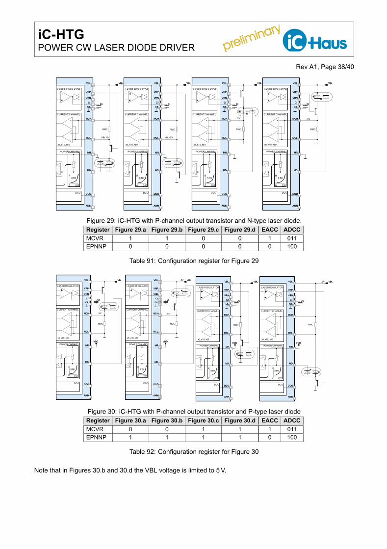
preliminary
preliminary iC-HTGPOWER CW LASER DIODE DRIVER
Rev A1, Page 38/40
N
N
N
N
+-
+- -
+ +-
CURRENTCHANNEL CURRENTCHANNELCURRENTCHANNELCURRENTCHANNEL
LASERREGULATOR LASERREGULATORLASERREGULATOR LASERREGULATOR
POWERCHANNELPOWERCHANNEL POWERCHANNEL POWERCHANNEL
x5,x10,x50 x5,x10,x50 x5,x10,x50x5,x10,x50
..VBL-5V ..VBL-5V
MCH
ANIN ANIN
DCO
RMC
ANIN
DCO
MCH
ANIN
DCODCO
RMCRMC
MCH MCH
DCO
RMC
DCODCO DCO
MCLMCL MCL MCL
VRP
VRN
VRPVRP
VRN
VRP
VRNVRN
8Bit 8Bit
..5V
8Bit 8Bit
...5V
VBLVBLVBLVBL VBLVBLVBL VBL
255255 255255
CI CI
++
CI
++
CI
MDMD MDMD
MR MR
CIL
MR
CILCIL
MR
CIL
- -- -CICICI CICI CICI CI
R
N
R
N
N
R
N
R
0
+
0
+
+
+
0
+
+
+
+
+
0
+
+
+
-
-
-
-
-
-
-
-
-
-
-
-
DCO
MCL
VRP +
DCO
+
MRMR
CIL
MCL
CI CI
+ VRP
VBL
VRN
VBL
ANIN
DCO
VRN
MR
VRP
VRN
MCH
MR
MCH
-CIL
ANIN
CIL
MD
VBLVBL
VRN -
MD
ANIN
MCL
MD
DCO
ANIN
CI
VBL
-
MCL
VBL
MD
-CI
VRP
MCH
+
MCH
CIL
VBL VBL
Figure 29: iC-HTG with P-channel output transistor and N-type laser diode.Register Figure 29.a Figure 29.b Figure 29.c Figure 29.d EACC ADCCMCVR 1 1 0 0 1 011EPNNP 0 0 0 0 0 100
Table 91: Configuration register for Figure 29
P
P
P
P
-+
-+
-+ +
-
CURRENTCHANNELCURRENTCHANNEL CURRENTCHANNEL CURRENTCHANNEL
LASERREGULATOR LASERREGULATOR LASERREGULATORLASERREGULATOR
POWERCHANNEL POWERCHANNELPOWERCHANNEL POWERCHANNEL
x5,x10,x50x5,x10,x50 x5,x10,x50x5,x10,x50
ANIN
DCO DCO
MCH
DCO
MCH
DCO
RMC
ANIN
RMC
ANIN
MCH
RMC
DCO DCO
ANIN
MCH
DCODCO
RMC
VDD VDD VDDVDD
MCLMCL MCLMCL
VRP
VRNVRNVRN VRN
VRPVRP VRP
8Bit8Bit
...5V ..5V
8Bit 8Bit
VBLVBLVBL VBLVBL VBLVBL VBL..5V
..5V
255255 255255
CI
+
CI
+
CI
+
CI
+
MD MDMD MD
CIL
MR MR MR
CILCIL
MR
CIL
- - --CI CI CI
CI CI CICI CI
P
R RR
P
R
P
P
+
0
+
+
0
+
+
+
0
++
+
0
+
+
+
-
-
-
- -
-
-
- -
- --
+
CI-
MCH
ANIN
MCL
ANIN
DCO
VRP
MR
MD
CIL
MCL
VRP
MCL
MCH
MR
MD
-
DCO
VBL
MR
VRP+
CIVRN-
MD
VRN
VBLVBL
VRN
CICI
DCO
VBL
CIL
VDD
MCH
VBL
-
MD
ANIN
CIL
VRP
MCH
CIL
ANIN
VDD
DCO
+
MCL
MR
+
VBL
VDD
VBL
VRN
VDD
VBL
Figure 30: iC-HTG with P-channel output transistor and P-type laser diodeRegister Figure 30.a Figure 30.b Figure 30.c Figure 30.d EACC ADCCMCVR 0 0 1 1 1 011EPNNP 1 1 1 1 0 100
Table 92: Configuration register for Figure 30
Note that in Figures 30.b and 30.d the VBL voltage is limited to 5 V.

preliminary
preliminary iC-HTGPOWER CW LASER DIODE DRIVER
Rev A1, Page 39/40
DESIGN REVIEW: Notes On Chip Functions
iC-HTG Z, Z1No. Function, Parameter/Code Description and Application Notes1 NEBUF For iC-HTG chip releases Z and Z1 it is NOT recommended to use NEBUF = 0.
Otherwise, proper operation of the control loop can not be guaranteed for allconditions. The parameter NEBUF does not exist anymore with iC-HTG chiprelease Y or higher. For iC-HTG chip releases see Table 58.
Table 93: Notes on chip functions regarding iC-HTG chip release Z and Z1.
REVISION HISTORY
Rel. Rel. Date∗ Chapter Modification PageA1 2017-11-24 Initial release
iC-Haus expressly reserves the right to change its products and/or specifications. An Infoletter gives details as to any amendments and additions made to therelevant current specifications on our internet website www.ichaus.com/infoletter and is automatically generated and shall be sent to registered users by email.Copying – even as an excerpt – is only permitted with iC-Haus’ approval in writing and precise reference to source.
The data specified is intended solely for the purpose of product description and shall represent the usual quality of the product. In case the specifications containobvious mistakes e.g. in writing or calculation, iC-Haus reserves the right to correct the specification and no liability arises insofar that the specification was froma third party view obviously not reliable. There shall be no claims based on defects as to quality in cases of insignificant deviations from the specifications or incase of only minor impairment of usability.No representations or warranties, either expressed or implied, of merchantability, fitness for a particular purpose or of any other nature are made hereunderwith respect to information/specification or the products to which information refers and no guarantee with respect to compliance to the intended use is given. Inparticular, this also applies to the stated possible applications or areas of applications of the product.
iC-Haus products are not designed for and must not be used in connection with any applications where the failure of such products would reasonably beexpected to result in significant personal injury or death (Safety-Critical Applications) without iC-Haus’ specific written consent. Safety-Critical Applicationsinclude, without limitation, life support devices and systems. iC-Haus products are not designed nor intended for use in military or aerospace applications orenvironments or in automotive applications unless specifically designated for such use by iC-Haus.iC-Haus conveys no patent, copyright, mask work right or other trade mark right to this product. iC-Haus assumes no liability for any patent and/or other trademark rights of a third party resulting from processing or handling of the product and/or any other use of the product.
Software and its documentation is provided by iC-Haus GmbH or contributors "AS IS" and is subject to the ZVEI General Conditions for the Supply of Productsand Services with iC-Haus amendments and the ZVEI Software clause with iC-Haus amendments (www.ichaus.com/EULA).
∗ Release Date format: YYYY-MM-DD

preliminary
preliminary iC-HTGPOWER CW LASER DIODE DRIVER
Rev A1, Page 40/40
ORDERING INFORMATION
Type Package Order Designation
iC-HTG QFN24 4 mm x 4 mm iC-HTG QFN24-4x4
EvaluationBoard
100 mm x 80 mm eval board iC-HTG EVAL HTG1D
Please send your purchase orders to our order handling team:
Fax: +49 (0) 61 35 - 92 92 - 692E-Mail: [email protected]
For technical support, information about prices and terms of delivery please contact:
iC-Haus GmbH Tel.: +49 (0) 61 35 - 92 92 - 0Am Kuemmerling 18 Fax: +49 (0) 61 35 - 92 92 - 192D-55294 Bodenheim Web: http://www.ichaus.comGERMANY E-Mail: [email protected]
Appointed local distributors: http://www.ichaus.com/sales_partners