ic compiler ii implementation user guide...chapter 1: contents contents 1-ixix ic compiler ii...
TRANSCRIPT

IC Compiler™ IIImplementationUser Guide
Version L-2016.03-SP4, September 2016

Copyright Notice and Proprietary Information©2016 Synopsys, Inc. All rights reserved. This Synopsys software and all associated documentation are proprietary to Synopsys, Inc. and may only be used pursuant to the terms and conditions of a written license agreement with Synopsys, Inc. All other use, reproduction, modification, or distribution of the Synopsys software or the associated documentation is strictly prohibited.
Destination Control StatementAll technical data contained in this publication is subject to the export control laws of the United States of America. Disclosure to nationals of other countries contrary to United States law is prohibited. It is the reader's responsibility to determine the applicable regulations and to comply with them.
DisclaimerSYNOPSYS, INC., AND ITS LICENSORS MAKE NO WARRANTY OF ANY KIND, EXPRESS OR IMPLIED, WITH REGARD TO THIS MATERIAL, INCLUDING, BUT NOT LIMITED TO, THE IMPLIED WARRANTIES OF MERCHANTABILITY AND FITNESS FOR A PARTICULAR PURPOSE.
TrademarksSynopsys and certain Synopsys product names are trademarks of Synopsys, as set forth athttp://www.synopsys.com/Company/Pages/Trademarks.aspx.All other product or company names may be trademarks of their respective owners.
Third-Party LinksAny links to third-party websites included in this document are for your convenience only. Synopsys does not endorse and is not responsible for such websites and their practices, including privacy practices, availability, and content.
Synopsys, Inc.690 E. Middlefield RoadMountain View, CA 94043www.synopsys.com
IC Compiler™ II Implementation User Guide, Version L-2016.03-SP4 ii

Copyright Notice for the Command-Line Editing Feature© 1992, 1993 The Regents of the University of California. All rights reserved. This code is derived from software contributed to Berkeley by Christos Zoulas of Cornell University.
Redistribution and use in source and binary forms, with or without modification, are permitted provided that the following conditions are met:1.Redistributions of source code must retain the above copyright notice, this list of conditions and the following
disclaimer.2.Redistributions in binary form must reproduce the above copyright notice, this list of conditions and the following
disclaimer in the documentation and/or other materials provided with the distribution.3.All advertising materials mentioning features or use of this software must display the following acknowledgement:
This product includes software developed by the University of California, Berkeley and its contributors.
4.Neither the name of the University nor the names of its contributors may be used to endorse or promote products derived from this software without specific prior written permission.
THIS SOFTWARE IS PROVIDED BY THE REGENTS AND CONTRIBUTORS "AS IS" AND ANY EXPRESS OR IMPLIED WARRANTIES, INCLUDING, BUT NOT LIMITED TO, THE IMPLIED WARRANTIES OF MERCHANTABILITY AND FITNESS FOR A PARTICULAR PURPOSE ARE DISCLAIMED. IN NO EVENT SHALL THE REGENTS OR CONTRIBUTORS BE LIABLE FOR ANY DIRECT, INDIRECT, INCIDENTAL, SPECIAL, EXEMPLARY, OR CONSEQUENTIAL DAMAGES (INCLUDING, BUT NOT LIMITED TO, PROCUREMENT OF SUBSTITUTE GOODS OR SERVICES; LOSS OF USE, DATA, OR PROFITS; OR BUSINESS INTERRUPTION) HOWEVER CAUSED AND ON ANY THEORY OF LIABILITY, WHETHER IN CONTRACT, STRICT LIABILITY, OR TORT (INCLUDING NEGLIGENCE OR OTHERWISE) ARISING IN ANY WAY OUT OF THE USE OF THIS SOFTWARE, EVEN IF ADVISED OF THE POSSIBILITY OF SUCH DAMAGE.
Copyright Notice for the Line-Editing Library© 1992 Simmule Turner and Rich Salz. All rights reserved.
This software is not subject to any license of the American Telephone and Telegraph Company or of the Regents of the University of California.
Permission is granted to anyone to use this software for any purpose on any computer system, and to alter it and redistribute it freely, subject to the following restrictions: 1.The authors are not responsible for the consequences of use of this software, no matter how awful, even if they arise
from flaws in it. 2.The origin of this software must not be misrepresented, either by explicit claim or by omission. Since few users ever
read sources, credits must appear in the documentation. 3.Altered versions must be plainly marked as such, and must not be misrepresented as being the original software.
Since few users ever read sources, credits must appear in the documentation. 4.This notice may not be removed or altered.
IC Compiler™ II Implementation User Guide, Version L-2016.03-SP4 iii

IC Compiler™ II Implementation User Guide, Version L-2016.03-SP4 iv

Contents
About This User Guide . . . . . . . . . . . . . . . . . . . . . . . . . . . . . . . . . . . . . . . . . . . . . . . xxii
Customer Support. . . . . . . . . . . . . . . . . . . . . . . . . . . . . . . . . . . . . . . . . . . . . . . . . . . xxiv
1. Working With the IC Compiler II Tool
Methodology Overview . . . . . . . . . . . . . . . . . . . . . . . . . . . . . . . . . . . . . . . . . . . . . . . 1-3
IC Compiler II Concepts . . . . . . . . . . . . . . . . . . . . . . . . . . . . . . . . . . . . . . . . . . . . . . 1-5
Power Intent Concepts . . . . . . . . . . . . . . . . . . . . . . . . . . . . . . . . . . . . . . . . . . . 1-5UPF Concepts . . . . . . . . . . . . . . . . . . . . . . . . . . . . . . . . . . . . . . . . . . . . . . 1-5UPF Flows . . . . . . . . . . . . . . . . . . . . . . . . . . . . . . . . . . . . . . . . . . . . . . . . . 1-6
Multiple-Patterning Concepts. . . . . . . . . . . . . . . . . . . . . . . . . . . . . . . . . . . . . . . 1-8Mask Constraints . . . . . . . . . . . . . . . . . . . . . . . . . . . . . . . . . . . . . . . . . . . . 1-10
User Interfaces . . . . . . . . . . . . . . . . . . . . . . . . . . . . . . . . . . . . . . . . . . . . . . . . . . . . . 1-11
Starting the Command-Line Interface . . . . . . . . . . . . . . . . . . . . . . . . . . . . . . . . 1-12
Exiting the IC Compiler II Tool . . . . . . . . . . . . . . . . . . . . . . . . . . . . . . . . . . . . . . 1-13
Entering icc2_shell Commands . . . . . . . . . . . . . . . . . . . . . . . . . . . . . . . . . . . . . . . . 1-13
Interrupting or Terminating Command Processing . . . . . . . . . . . . . . . . . . . . . . 1-14
Getting Information About Commands . . . . . . . . . . . . . . . . . . . . . . . . . . . . . . . 1-14Displaying Command Help . . . . . . . . . . . . . . . . . . . . . . . . . . . . . . . . . . . . . 1-15
Using Application Options. . . . . . . . . . . . . . . . . . . . . . . . . . . . . . . . . . . . . . . . . . . . . 1-15
Using Variables . . . . . . . . . . . . . . . . . . . . . . . . . . . . . . . . . . . . . . . . . . . . . . . . . . . . . 1-16
Viewing Man Pages . . . . . . . . . . . . . . . . . . . . . . . . . . . . . . . . . . . . . . . . . . . . . . . . . 1-16
Using Tcl Scripts . . . . . . . . . . . . . . . . . . . . . . . . . . . . . . . . . . . . . . . . . . . . . . . . . . . . 1-17
Using Setup Files . . . . . . . . . . . . . . . . . . . . . . . . . . . . . . . . . . . . . . . . . . . . . . . . . . . 1-18
v

IC Compiler™ II Implementation User Guide L-2016.03-SP4IC Compiler™ II Implementation User Guide Version L-2016.03-SP4
Using the Command Log File . . . . . . . . . . . . . . . . . . . . . . . . . . . . . . . . . . . . . . . . . . 1-19
2. Preparing the Design
Defining the Search Path . . . . . . . . . . . . . . . . . . . . . . . . . . . . . . . . . . . . . . . . . . . . . 2-3
Working With Design Libraries . . . . . . . . . . . . . . . . . . . . . . . . . . . . . . . . . . . . . . . . . 2-3
Working With Designs. . . . . . . . . . . . . . . . . . . . . . . . . . . . . . . . . . . . . . . . . . . . . . . . 2-4
Annotating the Floorplan Information . . . . . . . . . . . . . . . . . . . . . . . . . . . . . . . . . . . . 2-6
Reading DEF Files. . . . . . . . . . . . . . . . . . . . . . . . . . . . . . . . . . . . . . . . . . . . . . . 2-6Fixing Site Name Mismatches . . . . . . . . . . . . . . . . . . . . . . . . . . . . . . . . . . 2-7Validating DEF Files . . . . . . . . . . . . . . . . . . . . . . . . . . . . . . . . . . . . . . . . . . 2-7
Inheriting Port Locations . . . . . . . . . . . . . . . . . . . . . . . . . . . . . . . . . . . . . . . . . . 2-7
Annotating the Scan Chain Information . . . . . . . . . . . . . . . . . . . . . . . . . . . . . . . . . . 2-8
Loading a SCANDEF File . . . . . . . . . . . . . . . . . . . . . . . . . . . . . . . . . . . . . . . . . 2-8
Loading the Power Intent . . . . . . . . . . . . . . . . . . . . . . . . . . . . . . . . . . . . . . . . . . . . . 2-8
Preparing for Timing Analysis . . . . . . . . . . . . . . . . . . . . . . . . . . . . . . . . . . . . . . . . . . 2-10
Preparing the Power Network . . . . . . . . . . . . . . . . . . . . . . . . . . . . . . . . . . . . . . . . . . 2-10
Creating Logical Power and Ground Connections. . . . . . . . . . . . . . . . . . . . . . . 2-10
Creating Floating Logical Supply Nets. . . . . . . . . . . . . . . . . . . . . . . . . . . . . . . . 2-12
Verifying the Power Network Definition . . . . . . . . . . . . . . . . . . . . . . . . . . . . . . . 2-13
Preparing for Optimization . . . . . . . . . . . . . . . . . . . . . . . . . . . . . . . . . . . . . . . . . . . . 2-13
Restricting Library Cell Usage . . . . . . . . . . . . . . . . . . . . . . . . . . . . . . . . . . . . . . 2-14
Restricting the Target Libraries Used. . . . . . . . . . . . . . . . . . . . . . . . . . . . . . . . . 2-15
Preventing Optimization on Cells and Nets . . . . . . . . . . . . . . . . . . . . . . . . . . . . 2-16
Restricting Optimization on Cells. . . . . . . . . . . . . . . . . . . . . . . . . . . . . . . . . . . . 2-17
Preserving Pin Names During Sizing. . . . . . . . . . . . . . . . . . . . . . . . . . . . . . . . . 2-17
Isolating Input and Output Ports . . . . . . . . . . . . . . . . . . . . . . . . . . . . . . . . . . . . 2-18
Preparing for Percentage Low-Threshold-Voltage Optimization. . . . . . . . . . . . . . . . 2-19
Identifying Multiple-Threshold-Voltage Cells . . . . . . . . . . . . . . . . . . . . . . . . . . . 2-19
Constraining the Number of Low-Threshold-Voltage Cells . . . . . . . . . . . . . . . . 2-20
Annotating the Switching Activity . . . . . . . . . . . . . . . . . . . . . . . . . . . . . . . . . . . . . . . 2-21
Scaling the Switching Activity . . . . . . . . . . . . . . . . . . . . . . . . . . . . . . . . . . . . . . 2-21
Saving the Switching Activity When Saving the Design Library . . . . . . . . . . . . 2-22
Specifying the Routing Resources . . . . . . . . . . . . . . . . . . . . . . . . . . . . . . . . . . . . . . 2-22
Contents vi

IC Compiler™ II Implementation User Guide Version L-2016.03-SP4
Specifying the Global Layer Constraints . . . . . . . . . . . . . . . . . . . . . . . . . . . . . . 2-23Reporting Global Layer Constraints . . . . . . . . . . . . . . . . . . . . . . . . . . . . . . 2-24Removing Global Layer Constraints . . . . . . . . . . . . . . . . . . . . . . . . . . . . . . 2-24
Specifying Net-Specific Layer Constraints . . . . . . . . . . . . . . . . . . . . . . . . . . . . . 2-25Removing Net-Specific Routing Layer Constraints. . . . . . . . . . . . . . . . . . . 2-26
Specifying Clock-Tree Layer Constraints. . . . . . . . . . . . . . . . . . . . . . . . . . . . . . 2-26Removing Net-Specific Routing Layer Constraints. . . . . . . . . . . . . . . . . . . 2-27
Setting the Preferred Routing Direction for Layers . . . . . . . . . . . . . . . . . . . . . . 2-27
Enabling Multicore Processing . . . . . . . . . . . . . . . . . . . . . . . . . . . . . . . . . . . . . . . . . 2-28
Configuring Multithreading. . . . . . . . . . . . . . . . . . . . . . . . . . . . . . . . . . . . . . . . . 2-29
Configuring Distributed Processing . . . . . . . . . . . . . . . . . . . . . . . . . . . . . . . . . . 2-30
Reporting Multicore Configurations . . . . . . . . . . . . . . . . . . . . . . . . . . . . . . . . . . 2-31
Removing Multicore Configurations. . . . . . . . . . . . . . . . . . . . . . . . . . . . . . . . . . 2-31
Enabling Parallel Command Execution . . . . . . . . . . . . . . . . . . . . . . . . . . . . . . . 2-31
Supported Commands for Parallel Execution . . . . . . . . . . . . . . . . . . . . . . . . . . 2-32
3. Placement and Optimization
Placement and Optimization Concepts. . . . . . . . . . . . . . . . . . . . . . . . . . . . . . . . . . . 3-2
Placement Constraints . . . . . . . . . . . . . . . . . . . . . . . . . . . . . . . . . . . . . . . . . . . . . . . 3-2
Placement Blockages . . . . . . . . . . . . . . . . . . . . . . . . . . . . . . . . . . . . . . . . . . . . 3-2Keepout Margins. . . . . . . . . . . . . . . . . . . . . . . . . . . . . . . . . . . . . . . . . . . . . 3-3Area-Based Placement Blockages . . . . . . . . . . . . . . . . . . . . . . . . . . . . . . . 3-3
Placement Bounds. . . . . . . . . . . . . . . . . . . . . . . . . . . . . . . . . . . . . . . . . . . . . . . 3-4
Voltage Areas . . . . . . . . . . . . . . . . . . . . . . . . . . . . . . . . . . . . . . . . . . . . . . . . . . 3-5
Density Constraints . . . . . . . . . . . . . . . . . . . . . . . . . . . . . . . . . . . . . . . . . . . . . . 3-6
Cell Spacing Constraints . . . . . . . . . . . . . . . . . . . . . . . . . . . . . . . . . . . . . . . . . . 3-6
Preparing for Placement and Optimization . . . . . . . . . . . . . . . . . . . . . . . . . . . . . . . . 3-6
Defining Keepout Margins . . . . . . . . . . . . . . . . . . . . . . . . . . . . . . . . . . . . . . . . . 3-7Defining an Outer Keepout Margin . . . . . . . . . . . . . . . . . . . . . . . . . . . . . . . 3-7Defining an Inner Keepout Margin . . . . . . . . . . . . . . . . . . . . . . . . . . . . . . . 3-8
Defining Area-Based Placement Blockages . . . . . . . . . . . . . . . . . . . . . . . . . . . 3-8Defining a Hard Placement Blockage. . . . . . . . . . . . . . . . . . . . . . . . . . . . . 3-8Defining a Hard Macro Placement Blockage . . . . . . . . . . . . . . . . . . . . . . . 3-9Defining a Soft Placement Blockage . . . . . . . . . . . . . . . . . . . . . . . . . . . . . 3-9Defining a Partial Placement Blockage. . . . . . . . . . . . . . . . . . . . . . . . . . . . 3-10Querying Placement Blockages . . . . . . . . . . . . . . . . . . . . . . . . . . . . . . . . . 3-10Removing Placement Blockages . . . . . . . . . . . . . . . . . . . . . . . . . . . . . . . . 3-10
Chapter 1: Contents1-viiContents vii

IC Compiler™ II Implementation User Guide L-2016.03-SP4IC Compiler™ II Implementation User Guide Version L-2016.03-SP4
Defining Placement Bounds . . . . . . . . . . . . . . . . . . . . . . . . . . . . . . . . . . . . . . . 3-10Defining Move Bounds . . . . . . . . . . . . . . . . . . . . . . . . . . . . . . . . . . . . . . . . 3-11Defining Group Bounds . . . . . . . . . . . . . . . . . . . . . . . . . . . . . . . . . . . . . . . 3-12Querying Placement Bounds . . . . . . . . . . . . . . . . . . . . . . . . . . . . . . . . . . . 3-13Removing Placement Bounds . . . . . . . . . . . . . . . . . . . . . . . . . . . . . . . . . . 3-13
Generating Automatic Group Bounds for Clock Gating Cells . . . . . . . . . . . . . . 3-13
Defining Voltage Areas . . . . . . . . . . . . . . . . . . . . . . . . . . . . . . . . . . . . . . . . . . . 3-14Merging Voltage Area Shapes . . . . . . . . . . . . . . . . . . . . . . . . . . . . . . . . . . 3-15Resolving Overlapping Voltage Areas . . . . . . . . . . . . . . . . . . . . . . . . . . . . 3-16Modifying the Stacking Order . . . . . . . . . . . . . . . . . . . . . . . . . . . . . . . . . . . 3-17Defining Guard Bands . . . . . . . . . . . . . . . . . . . . . . . . . . . . . . . . . . . . . . . . 3-18Querying Voltage Areas . . . . . . . . . . . . . . . . . . . . . . . . . . . . . . . . . . . . . . . 3-20Modifying Voltage Areas . . . . . . . . . . . . . . . . . . . . . . . . . . . . . . . . . . . . . . . 3-20Removing Voltage Areas . . . . . . . . . . . . . . . . . . . . . . . . . . . . . . . . . . . . . . 3-21
Controlling the Placement Density. . . . . . . . . . . . . . . . . . . . . . . . . . . . . . . . . . . 3-21
Defining Cell Spacing Constraints . . . . . . . . . . . . . . . . . . . . . . . . . . . . . . . . . . . 3-21Reporting Cell Spacing Constraints . . . . . . . . . . . . . . . . . . . . . . . . . . . . . . 3-23Removing Cell Spacing Constraints . . . . . . . . . . . . . . . . . . . . . . . . . . . . . . 3-23
Inserting Multivoltage Cells . . . . . . . . . . . . . . . . . . . . . . . . . . . . . . . . . . . . . . . . 3-23Inserting Level Shifters . . . . . . . . . . . . . . . . . . . . . . . . . . . . . . . . . . . . . . . . 3-24Inserting Isolation Cells. . . . . . . . . . . . . . . . . . . . . . . . . . . . . . . . . . . . . . . . 3-24Associating Power Strategies With Existing Multivoltage Cells . . . . . . . . . 3-24Analyzing Multivoltage Cells . . . . . . . . . . . . . . . . . . . . . . . . . . . . . . . . . . . . 3-25
Marking the Clock Networks . . . . . . . . . . . . . . . . . . . . . . . . . . . . . . . . . . . . . . . 3-25
Performing Placement and Optimization . . . . . . . . . . . . . . . . . . . . . . . . . . . . . . . . . 3-25
Introduction to Power Optimization . . . . . . . . . . . . . . . . . . . . . . . . . . . . . . . . . . 3-26
Performing Power Optimization . . . . . . . . . . . . . . . . . . . . . . . . . . . . . . . . . . . . . 3-26Performing Low-Power Placement . . . . . . . . . . . . . . . . . . . . . . . . . . . . . . . 3-27Performing Conventional Leakage-Power Optimization . . . . . . . . . . . . . . . 3-27Performing Dynamic-Power Optimization. . . . . . . . . . . . . . . . . . . . . . . . . . 3-27Performing Total-Power Optimization . . . . . . . . . . . . . . . . . . . . . . . . . . . . . 3-28Performing Percentage Low-Threshold-Voltage Optimization . . . . . . . . . . 3-28
Enabling Scan Chain Optimization . . . . . . . . . . . . . . . . . . . . . . . . . . . . . . . . . . 3-29
Enabling the Automatic Use of Nondefault Routing Rules During Preroute Optimization3-30
Enabling Global-Route-Based RC Estimation During Preroute Optimization . . 3-31
Defining a Cell Name Prefix for Optimization . . . . . . . . . . . . . . . . . . . . . . . . . . 3-32
Performing Standalone Placement and Legalization . . . . . . . . . . . . . . . . . . . . . 3-32
Performing Placement, Optimization, and Legalization With a Single Command 3-33
Contents viii

IC Compiler™ II Implementation User Guide Version L-2016.03-SP4
Considering the Impact on Clock Structures During Placement . . . . . . . . . 3-34Creating a Temporary Clock Tree for Placement and Optimization . . . . . . 3-35Optimizing Integrated Clock-Gating Logic . . . . . . . . . . . . . . . . . . . . . . . . . 3-35Enabling Global Route Based High-Fanout Synthesis . . . . . . . . . . . . . . . . 3-36Changing the Congestion Effort . . . . . . . . . . . . . . . . . . . . . . . . . . . . . . . . . 3-36Enabling Layer Optimization. . . . . . . . . . . . . . . . . . . . . . . . . . . . . . . . . . . . 3-37Enabling Path Optimization . . . . . . . . . . . . . . . . . . . . . . . . . . . . . . . . . . . . 3-37
Using Physical Guidance From the Design Compiler Tool . . . . . . . . . . . . . . . . 3-37
Performing Multibit Banking. . . . . . . . . . . . . . . . . . . . . . . . . . . . . . . . . . . . . . . . 3-39Identifying Multibit Banks . . . . . . . . . . . . . . . . . . . . . . . . . . . . . . . . . . . . . . 3-40Splitting Multibit Banks . . . . . . . . . . . . . . . . . . . . . . . . . . . . . . . . . . . . . . . . 3-42
Performing Incremental Placement and Optimization . . . . . . . . . . . . . . . . . . . . 3-43Optimizing Specific Endpoints . . . . . . . . . . . . . . . . . . . . . . . . . . . . . . . . . . 3-44Enabling Layer Optimization During Path Optimization . . . . . . . . . . . . . . . 3-44
Performing Magnet Placement . . . . . . . . . . . . . . . . . . . . . . . . . . . . . . . . . . . . . 3-44
Refining Placement . . . . . . . . . . . . . . . . . . . . . . . . . . . . . . . . . . . . . . . . . . . . . . 3-46
Performing Placement and Optimization on Multivoltage Blocks . . . . . . . . . . . 3-46
Analyzing the Placement and Optimization Results . . . . . . . . . . . . . . . . . . . . . . . . . 3-47
Analyzing the Bufferability of Nets . . . . . . . . . . . . . . . . . . . . . . . . . . . . . . . . . . . 3-47
Reporting Utilization. . . . . . . . . . . . . . . . . . . . . . . . . . . . . . . . . . . . . . . . . . . . . . 3-48
Reporting the Placement QoR. . . . . . . . . . . . . . . . . . . . . . . . . . . . . . . . . . . . . . 3-50
Querying and Changing the Placement Status . . . . . . . . . . . . . . . . . . . . . . . . . 3-52
Analyzing the Placement in the GUI . . . . . . . . . . . . . . . . . . . . . . . . . . . . . . . . . 3-53Cell Density Map. . . . . . . . . . . . . . . . . . . . . . . . . . . . . . . . . . . . . . . . . . . . . 3-53Pin Density Map . . . . . . . . . . . . . . . . . . . . . . . . . . . . . . . . . . . . . . . . . . . . . 3-57Global Route Congestion Map . . . . . . . . . . . . . . . . . . . . . . . . . . . . . . . . . . 3-60
Analyzing the Timing. . . . . . . . . . . . . . . . . . . . . . . . . . . . . . . . . . . . . . . . . . . . . . . . . 3-62
Generating Timing Reports . . . . . . . . . . . . . . . . . . . . . . . . . . . . . . . . . . . . . . . . 3-62Reporting the Worst-Case Timing Paths . . . . . . . . . . . . . . . . . . . . . . . . . . 3-62Reporting the QoR . . . . . . . . . . . . . . . . . . . . . . . . . . . . . . . . . . . . . . . . . . . 3-65Reporting the Logical DRC Violations . . . . . . . . . . . . . . . . . . . . . . . . . . . . 3-67
Analyzing Violations That Cannot Be Fixed. . . . . . . . . . . . . . . . . . . . . . . . . . . . 3-69
Analyzing the Power . . . . . . . . . . . . . . . . . . . . . . . . . . . . . . . . . . . . . . . . . . . . . . . . . 3-70
Creating Power Groups for Reporting . . . . . . . . . . . . . . . . . . . . . . . . . . . . . . . . 3-71
Reporting Pin-Based Clock Network Power . . . . . . . . . . . . . . . . . . . . . . . . . . . 3-72
Chapter 1: Contents1-ixContents ix

IC Compiler™ II Implementation User Guide L-2016.03-SP4IC Compiler™ II Implementation User Guide Version L-2016.03-SP4
4. Clock Tree Synthesis
Prerequisites for Clock Tree Synthesis. . . . . . . . . . . . . . . . . . . . . . . . . . . . . . . . . . . 4-2
Analyzing the Presynthesized Clock Tree . . . . . . . . . . . . . . . . . . . . . . . . . . . . . . . . 4-2
Defining the Clock Trees. . . . . . . . . . . . . . . . . . . . . . . . . . . . . . . . . . . . . . . . . . . . . . 4-3
Deriving the Clock Trees . . . . . . . . . . . . . . . . . . . . . . . . . . . . . . . . . . . . . . . . . . 4-3Identifying the Clock Roots . . . . . . . . . . . . . . . . . . . . . . . . . . . . . . . . . . . . . 4-4Identifying the Clock Endpoints . . . . . . . . . . . . . . . . . . . . . . . . . . . . . . . . . 4-5
Defining Clock Tree Exceptions. . . . . . . . . . . . . . . . . . . . . . . . . . . . . . . . . . . . . 4-7Defining Sink Pins. . . . . . . . . . . . . . . . . . . . . . . . . . . . . . . . . . . . . . . . . . . . 4-8Defining Insertion Delay Requirements . . . . . . . . . . . . . . . . . . . . . . . . . . . 4-8Defining Ignore Pins . . . . . . . . . . . . . . . . . . . . . . . . . . . . . . . . . . . . . . . . . . 4-9Setting Don’t Touch Exceptions . . . . . . . . . . . . . . . . . . . . . . . . . . . . . . . . . 4-10Setting Size-Only Exceptions . . . . . . . . . . . . . . . . . . . . . . . . . . . . . . . . . . . 4-11
Copying Clock Tree Exceptions Across Modes . . . . . . . . . . . . . . . . . . . . . . . . . 4-12
Deriving Clock Tree Exceptions From Ideal Clock Latencies . . . . . . . . . . . . . . 4-12
Handling Endpoints With Balancing Conflicts . . . . . . . . . . . . . . . . . . . . . . . . . . 4-13
Verifying the Clock Trees . . . . . . . . . . . . . . . . . . . . . . . . . . . . . . . . . . . . . . . . . . . . . 4-15
Setting Clock Tree Design Rule Constraints. . . . . . . . . . . . . . . . . . . . . . . . . . . . . . . 4-17
Specifying the Clock Tree Synthesis Settings. . . . . . . . . . . . . . . . . . . . . . . . . . . . . . 4-18
Specifying the Clock Tree References. . . . . . . . . . . . . . . . . . . . . . . . . . . . . . . . 4-18Deriving Clock Tree References for Preexisting Gates . . . . . . . . . . . . . . . 4-19Restricting the Target Libraries Used . . . . . . . . . . . . . . . . . . . . . . . . . . . . . 4-20
Setting Skew and Latency Targets . . . . . . . . . . . . . . . . . . . . . . . . . . . . . . . . . . 4-20
Enabling Local Skew Optimization . . . . . . . . . . . . . . . . . . . . . . . . . . . . . . . . . . 4-21
Specifying the Primary Corner for Clock Tree Synthesis . . . . . . . . . . . . . . . . . . 4-21
Preserving Preexisting Clock Trees. . . . . . . . . . . . . . . . . . . . . . . . . . . . . . . . . . 4-22
Preserving the Clock Ports of Existing Hierarchies . . . . . . . . . . . . . . . . . . . . . . 4-22
Reducing Electromigration. . . . . . . . . . . . . . . . . . . . . . . . . . . . . . . . . . . . . . . . . 4-22
Handling Inaccurate Constraints During Clock Tree Synthesis . . . . . . . . . . . . . 4-23
Defining Clock Cell Spacing Rules . . . . . . . . . . . . . . . . . . . . . . . . . . . . . . . . . . 4-24
Creating Skew Groups. . . . . . . . . . . . . . . . . . . . . . . . . . . . . . . . . . . . . . . . . . . . 4-25
Defining a Name Prefix for Clock Cells . . . . . . . . . . . . . . . . . . . . . . . . . . . . . . . 4-25
Using the Global Router During Initial Clock Tree Synthesis. . . . . . . . . . . . . . . 4-26
Setting Clock Tree Routing Options. . . . . . . . . . . . . . . . . . . . . . . . . . . . . . . . . . 4-26
Reducing Signal Integrity Effects on Clock Nets . . . . . . . . . . . . . . . . . . . . . . . . 4-26
Reporting the Clock Tree Settings . . . . . . . . . . . . . . . . . . . . . . . . . . . . . . . . . . . 4-27
Contents x

IC Compiler™ II Implementation User Guide Version L-2016.03-SP4
Implementing Clock Trees . . . . . . . . . . . . . . . . . . . . . . . . . . . . . . . . . . . . . . . . . . . . 4-27
Performing Standalone Clock Trees Synthesis . . . . . . . . . . . . . . . . . . . . . . . . . 4-28
Synthesizing and Routing Clock Trees, and Optimizing the Design With a Single Command . . . . . . . . . . . . . . . . . . . . . . . . . . . . . . . . . . . . . . . . . . . . . . . . . . . . . 4-29
Performing Concurrent Clock and Data Optimization . . . . . . . . . . . . . . . . . . . . 4-30
Splitting Clock Cells . . . . . . . . . . . . . . . . . . . . . . . . . . . . . . . . . . . . . . . . . . . . . . 4-31
Balancing Skew Between Different Clock Trees . . . . . . . . . . . . . . . . . . . . . . . . 4-32Defining the Interclock Delay Balancing Constraints . . . . . . . . . . . . . . . . . 4-32Generating Interclock Delay Balancing Constraints Automatically . . . . . . . 4-34Running Interclock Delay Balancing . . . . . . . . . . . . . . . . . . . . . . . . . . . . . . 4-34
Optimizing the Design After Clock Tree Synthesis . . . . . . . . . . . . . . . . . . . . . . 4-35
Routing Clock Trees . . . . . . . . . . . . . . . . . . . . . . . . . . . . . . . . . . . . . . . . . . . . . 4-35
Performing Postroute Clock Tree Optimization . . . . . . . . . . . . . . . . . . . . . . . . . 4-35
Marking Clock Trees as Synthesized. . . . . . . . . . . . . . . . . . . . . . . . . . . . . . . . . 4-36
Removing Clock Trees. . . . . . . . . . . . . . . . . . . . . . . . . . . . . . . . . . . . . . . . . . . . 4-37
Implementing Multisource Clock Trees. . . . . . . . . . . . . . . . . . . . . . . . . . . . . . . . . . . 4-38
Introduction to Multisource Clock Trees. . . . . . . . . . . . . . . . . . . . . . . . . . . . . . . 4-39
Implementing Regular Multisource Clock Trees . . . . . . . . . . . . . . . . . . . . . . . . 4-41
Implementing Structural Multisource Clock Trees . . . . . . . . . . . . . . . . . . . . . . . 4-41
Inserting Clock Drivers. . . . . . . . . . . . . . . . . . . . . . . . . . . . . . . . . . . . . . . . . . . . 4-42
Synthesizing the Global Clock Trees . . . . . . . . . . . . . . . . . . . . . . . . . . . . . . . . . 4-45
Creating Clock Straps . . . . . . . . . . . . . . . . . . . . . . . . . . . . . . . . . . . . . . . . . . . . 4-47
Routing to Clock Straps . . . . . . . . . . . . . . . . . . . . . . . . . . . . . . . . . . . . . . . . . . . 4-51
Analyzing Clock Mesh . . . . . . . . . . . . . . . . . . . . . . . . . . . . . . . . . . . . . . . . . . . . 4-54
Performing Tap Assignment. . . . . . . . . . . . . . . . . . . . . . . . . . . . . . . . . . . . . . . . 4-56
Building the Local Clock Subtree Structures . . . . . . . . . . . . . . . . . . . . . . . . . . . 4-57
Analyzing the Clock Tree Results . . . . . . . . . . . . . . . . . . . . . . . . . . . . . . . . . . . . . . . 4-60
Generating Clock Tree QoR Reports. . . . . . . . . . . . . . . . . . . . . . . . . . . . . . . . . 4-60
Creating Collections of Clock Network Pins . . . . . . . . . . . . . . . . . . . . . . . . . . . 4-62
Analyzing Clock Timing . . . . . . . . . . . . . . . . . . . . . . . . . . . . . . . . . . . . . . . . . . . 4-63
Analyzing Clock Trees in the GUI . . . . . . . . . . . . . . . . . . . . . . . . . . . . . . . . . . . 4-63Using the Clock Tree Analysis Window . . . . . . . . . . . . . . . . . . . . . . . . . . . 4-64Viewing Clock Tree Schematics . . . . . . . . . . . . . . . . . . . . . . . . . . . . . . . . . 4-65Viewing Clock Graphs . . . . . . . . . . . . . . . . . . . . . . . . . . . . . . . . . . . . . . . . 4-65
5. Routing and Postroute Optimization
Introduction to Zroute . . . . . . . . . . . . . . . . . . . . . . . . . . . . . . . . . . . . . . . . . . . . . . . . 5-3
Chapter 1: Contents1-xiContents xi

IC Compiler™ II Implementation User Guide L-2016.03-SP4IC Compiler™ II Implementation User Guide Version L-2016.03-SP4
Basic Zroute Flow . . . . . . . . . . . . . . . . . . . . . . . . . . . . . . . . . . . . . . . . . . . . . . . . . . . 5-4
Prerequisites for Routing . . . . . . . . . . . . . . . . . . . . . . . . . . . . . . . . . . . . . . . . . . . . . 5-5
Defining Vias. . . . . . . . . . . . . . . . . . . . . . . . . . . . . . . . . . . . . . . . . . . . . . . . . . . . . . . 5-6
Reading Via Definitions from a LEF File . . . . . . . . . . . . . . . . . . . . . . . . . . . . . . 5-7
Creating a Via Definition . . . . . . . . . . . . . . . . . . . . . . . . . . . . . . . . . . . . . . . . . . 5-7Defining Simple Vias. . . . . . . . . . . . . . . . . . . . . . . . . . . . . . . . . . . . . . . . . . 5-7Defining Custom Vias . . . . . . . . . . . . . . . . . . . . . . . . . . . . . . . . . . . . . . . . . 5-8
Checking Routability . . . . . . . . . . . . . . . . . . . . . . . . . . . . . . . . . . . . . . . . . . . . . . . . . 5-10
Routing Constraints . . . . . . . . . . . . . . . . . . . . . . . . . . . . . . . . . . . . . . . . . . . . . . . . . 5-14
Defining Routing Blockages. . . . . . . . . . . . . . . . . . . . . . . . . . . . . . . . . . . . . . . . 5-16Reserving Space for Top-Level Routing . . . . . . . . . . . . . . . . . . . . . . . . . . . 5-17Querying Routing Blockages . . . . . . . . . . . . . . . . . . . . . . . . . . . . . . . . . . . 5-18Removing Routing Blockages. . . . . . . . . . . . . . . . . . . . . . . . . . . . . . . . . . . 5-18
Defining Routing Guides . . . . . . . . . . . . . . . . . . . . . . . . . . . . . . . . . . . . . . . . . . 5-18Using Routing Guides to Control the Routing Direction . . . . . . . . . . . . . . . 5-20Using Routing Guides to Limit Edges in the Nonpreferred Direction . . . . . 5-21Using Routing Guides to Control the Routing Density . . . . . . . . . . . . . . . . 5-22Using Routing Guides to Prioritize Routing Regions . . . . . . . . . . . . . . . . . 5-22Using Routing Guides to Encourage River Routing . . . . . . . . . . . . . . . . . . 5-23Querying Routing Guides . . . . . . . . . . . . . . . . . . . . . . . . . . . . . . . . . . . . . . 5-24Removing Routing Guides . . . . . . . . . . . . . . . . . . . . . . . . . . . . . . . . . . . . . 5-24
Routing Nets Within a Specific Region . . . . . . . . . . . . . . . . . . . . . . . . . . . . . . . 5-24Defining Routing Corridors . . . . . . . . . . . . . . . . . . . . . . . . . . . . . . . . . . . . . 5-25Assigning Nets to a Routing Corridor . . . . . . . . . . . . . . . . . . . . . . . . . . . . . 5-26Verifying Routing Corridors. . . . . . . . . . . . . . . . . . . . . . . . . . . . . . . . . . . . . 5-27Modifying Routing Corridors . . . . . . . . . . . . . . . . . . . . . . . . . . . . . . . . . . . . 5-27Reporting Routing Corridors . . . . . . . . . . . . . . . . . . . . . . . . . . . . . . . . . . . . 5-27Removing Routing Corridors . . . . . . . . . . . . . . . . . . . . . . . . . . . . . . . . . . . 5-28
Using Nondefault Routing Rules . . . . . . . . . . . . . . . . . . . . . . . . . . . . . . . . . . . . 5-28Defining Nondefault Routing Rules. . . . . . . . . . . . . . . . . . . . . . . . . . . . . . . 5-29Assigning Nondefault Routing Rules to Nets . . . . . . . . . . . . . . . . . . . . . . . 5-40
Controlling Off-Grid Routing . . . . . . . . . . . . . . . . . . . . . . . . . . . . . . . . . . . . . . . 5-43Preventing Off-Grid Routing . . . . . . . . . . . . . . . . . . . . . . . . . . . . . . . . . . . . 5-43Discouraging Off-Grid Routing for Vias . . . . . . . . . . . . . . . . . . . . . . . . . . . 5-44
Controlling Pin Connections . . . . . . . . . . . . . . . . . . . . . . . . . . . . . . . . . . . . . . . 5-45
Controlling Pin Tapering. . . . . . . . . . . . . . . . . . . . . . . . . . . . . . . . . . . . . . . . . . . 5-47Specifying the Tapering Method . . . . . . . . . . . . . . . . . . . . . . . . . . . . . . . . . 5-47Controlling the Tapering Width . . . . . . . . . . . . . . . . . . . . . . . . . . . . . . . . . . 5-49
Contents xii

IC Compiler™ II Implementation User Guide Version L-2016.03-SP4
Setting the Rerouting Mode . . . . . . . . . . . . . . . . . . . . . . . . . . . . . . . . . . . . . . . . 5-49
Routing Application Options . . . . . . . . . . . . . . . . . . . . . . . . . . . . . . . . . . . . . . . . . . . 5-50
Routing Multivoltage Designs . . . . . . . . . . . . . . . . . . . . . . . . . . . . . . . . . . . . . . . . . . 5-50
Routing Clock Nets . . . . . . . . . . . . . . . . . . . . . . . . . . . . . . . . . . . . . . . . . . . . . . . . . . 5-51
Routing Critical Nets . . . . . . . . . . . . . . . . . . . . . . . . . . . . . . . . . . . . . . . . . . . . . . . . . 5-52
Routing Secondary Power and Ground Pins . . . . . . . . . . . . . . . . . . . . . . . . . . . . . . 5-53
Verifying the Secondary Power and Ground Pin Attributes . . . . . . . . . . . . . . . . 5-53
Setting the Routing Constraints . . . . . . . . . . . . . . . . . . . . . . . . . . . . . . . . . . . . . 5-54
Routing the Secondary Power and Ground Pins . . . . . . . . . . . . . . . . . . . . . . . . 5-55
Routing Signal Nets . . . . . . . . . . . . . . . . . . . . . . . . . . . . . . . . . . . . . . . . . . . . . . . . . 5-56
Global Routing . . . . . . . . . . . . . . . . . . . . . . . . . . . . . . . . . . . . . . . . . . . . . . . . . . 5-57Global Routing During Design Planning . . . . . . . . . . . . . . . . . . . . . . . . . . . 5-60Timing-Driven Global Routing. . . . . . . . . . . . . . . . . . . . . . . . . . . . . . . . . . . 5-60Crosstalk-Driven Global Routing . . . . . . . . . . . . . . . . . . . . . . . . . . . . . . . . 5-60Incremental Global Routing . . . . . . . . . . . . . . . . . . . . . . . . . . . . . . . . . . . . 5-61
Track Assignment . . . . . . . . . . . . . . . . . . . . . . . . . . . . . . . . . . . . . . . . . . . . . . . 5-61
Detail Routing . . . . . . . . . . . . . . . . . . . . . . . . . . . . . . . . . . . . . . . . . . . . . . . . . . 5-62
Routing Signal Nets by Using Automatic Routing . . . . . . . . . . . . . . . . . . . . . . . 5-67
Shielding Nets. . . . . . . . . . . . . . . . . . . . . . . . . . . . . . . . . . . . . . . . . . . . . . . . . . . . . . 5-68
Defining the Shielding Rules . . . . . . . . . . . . . . . . . . . . . . . . . . . . . . . . . . . . . . . 5-70
Performing Preroute Shielding. . . . . . . . . . . . . . . . . . . . . . . . . . . . . . . . . . . . . . 5-70
Soft Shielding Rules During Signal Routing . . . . . . . . . . . . . . . . . . . . . . . . . . . 5-73
Performing Postroute Shielding . . . . . . . . . . . . . . . . . . . . . . . . . . . . . . . . . . . . . 5-73Shielding Example . . . . . . . . . . . . . . . . . . . . . . . . . . . . . . . . . . . . . . . . . . . 5-74
Performing Incremental Shielding . . . . . . . . . . . . . . . . . . . . . . . . . . . . . . . . . . . 5-75
Reporting Shielding Information . . . . . . . . . . . . . . . . . . . . . . . . . . . . . . . . . . . . 5-75
Performing Shielding Checks . . . . . . . . . . . . . . . . . . . . . . . . . . . . . . . . . . . . . . 5-76
Performing Postroute Optimization. . . . . . . . . . . . . . . . . . . . . . . . . . . . . . . . . . . . . . 5-77
Performing Postroute Logic Optimization . . . . . . . . . . . . . . . . . . . . . . . . . . . . . 5-77
Fixing DRC Violations Caused by Pin Access Issues . . . . . . . . . . . . . . . . . . . . 5-79
Analyzing and Fixing Signal Electromigration Violations . . . . . . . . . . . . . . . . . . . . . 5-80
Performing ECO Routing . . . . . . . . . . . . . . . . . . . . . . . . . . . . . . . . . . . . . . . . . . . . . 5-81
Routing Nets in the GUI . . . . . . . . . . . . . . . . . . . . . . . . . . . . . . . . . . . . . . . . . . . . . . 5-83
Modifying Routed Nets . . . . . . . . . . . . . . . . . . . . . . . . . . . . . . . . . . . . . . . . . . . 5-84
Chapter 1: Contents1-xiiiContents xiii

IC Compiler™ II Implementation User Guide L-2016.03-SP4IC Compiler™ II Implementation User Guide Version L-2016.03-SP4
Cleaning Up Routed Nets . . . . . . . . . . . . . . . . . . . . . . . . . . . . . . . . . . . . . . . . . . . . . 5-85
Analyzing the Routing Results . . . . . . . . . . . . . . . . . . . . . . . . . . . . . . . . . . . . . . . . . 5-86
Generating a Congestion Report . . . . . . . . . . . . . . . . . . . . . . . . . . . . . . . . . . . . 5-86
Generating a Congestion Map. . . . . . . . . . . . . . . . . . . . . . . . . . . . . . . . . . . . . . 5-88
Performing Design Rule Checking Using Zroute . . . . . . . . . . . . . . . . . . . . . . . . 5-90
Performing Signoff Design Rule Checking . . . . . . . . . . . . . . . . . . . . . . . . . . . . 5-93
Performing Design Rule Checking in an External Tool . . . . . . . . . . . . . . . . . . . 5-93
Performing Layout-Versus-Schematic Checking . . . . . . . . . . . . . . . . . . . . . . . . 5-94
Reporting the Routing Results. . . . . . . . . . . . . . . . . . . . . . . . . . . . . . . . . . . . . . 5-95
Using the DRC Query Commands. . . . . . . . . . . . . . . . . . . . . . . . . . . . . . . . . . . 5-96
Saving Route Information . . . . . . . . . . . . . . . . . . . . . . . . . . . . . . . . . . . . . . . . . . . . . 5-96
6. Chip Finishing and Design for Manufacturing
Inserting Tap Cells . . . . . . . . . . . . . . . . . . . . . . . . . . . . . . . . . . . . . . . . . . . . . . . . . . 6-2
Inserting Boundary Cells. . . . . . . . . . . . . . . . . . . . . . . . . . . . . . . . . . . . . . . . . . . . . . 6-5
Specifying the Boundary Cell Insertion Requirements. . . . . . . . . . . . . . . . . . . . 6-5Specifying the Library Cells for Boundary Cell Insertion. . . . . . . . . . . . . . . 6-6Specifying Boundary Cell Placement Rules . . . . . . . . . . . . . . . . . . . . . . . . 6-7Specifying the Naming Convention for Boundary Cells . . . . . . . . . . . . . . . 6-8
Reporting the Boundary Cell Insertion Requirements . . . . . . . . . . . . . . . . . . . . 6-9
Removing Boundary Cell Insertion Requirements. . . . . . . . . . . . . . . . . . . . . . . 6-9
Verifying the Boundary Cell Placement . . . . . . . . . . . . . . . . . . . . . . . . . . . . . . . 6-9
Finding and Fixing Antenna Violations . . . . . . . . . . . . . . . . . . . . . . . . . . . . . . . . . . . 6-10
Defining Metal Layer Antenna Rules . . . . . . . . . . . . . . . . . . . . . . . . . . . . . . . . . 6-10Defining the Global Metal Layer Antenna Rules. . . . . . . . . . . . . . . . . . . . . 6-11Defining Layer-Specific Antenna Rules . . . . . . . . . . . . . . . . . . . . . . . . . . . 6-16
Specifying Antenna Properties. . . . . . . . . . . . . . . . . . . . . . . . . . . . . . . . . . . . . . 6-22
Analyzing and Fixing Antenna Violations. . . . . . . . . . . . . . . . . . . . . . . . . . . . . . 6-23Inserting Diodes During Detail Routing. . . . . . . . . . . . . . . . . . . . . . . . . . . . 6-25Inserting Diodes After Detail Routing . . . . . . . . . . . . . . . . . . . . . . . . . . . . . 6-26
Inserting Redundant Vias . . . . . . . . . . . . . . . . . . . . . . . . . . . . . . . . . . . . . . . . . . . . . 6-27
Inserting Redundant Vias on Clock Nets . . . . . . . . . . . . . . . . . . . . . . . . . . . . . . 6-27
Inserting Redundant Vias on Signal Nets . . . . . . . . . . . . . . . . . . . . . . . . . . . . . 6-28Viewing the Default Via Mapping Table . . . . . . . . . . . . . . . . . . . . . . . . . . . 6-29Defining a Customized Via Mapping Table . . . . . . . . . . . . . . . . . . . . . . . . . 6-30Postroute Redundant Via Insertion. . . . . . . . . . . . . . . . . . . . . . . . . . . . . . . 6-31
Contents xiv

IC Compiler™ II Implementation User Guide Version L-2016.03-SP4
Concurrent Soft-Rule-Based Redundant Via Insertion . . . . . . . . . . . . . . . . 6-32Near 100 Percent Redundant Via Insertion . . . . . . . . . . . . . . . . . . . . . . . . 6-33Preserving Timing During Redundant Via Insertion . . . . . . . . . . . . . . . . . . 6-34Reporting Redundant Via Rates . . . . . . . . . . . . . . . . . . . . . . . . . . . . . . . . . 6-35
Optimizing Wire Length and Via Count. . . . . . . . . . . . . . . . . . . . . . . . . . . . . . . . . . . 6-36
Reducing Critical Areas . . . . . . . . . . . . . . . . . . . . . . . . . . . . . . . . . . . . . . . . . . . . . . 6-37
Performing Wire Spreading . . . . . . . . . . . . . . . . . . . . . . . . . . . . . . . . . . . . . . . . 6-37
Performing Wire Widening. . . . . . . . . . . . . . . . . . . . . . . . . . . . . . . . . . . . . . . . . 6-38
Inserting Filler Cells . . . . . . . . . . . . . . . . . . . . . . . . . . . . . . . . . . . . . . . . . . . . . . . . . 6-39
Standard Filler Cell Insertion . . . . . . . . . . . . . . . . . . . . . . . . . . . . . . . . . . . . . . . 6-40Controlling Standard Filler Cell Insertion . . . . . . . . . . . . . . . . . . . . . . . . . . 6-41Checking for Filler Cell DRC Violations . . . . . . . . . . . . . . . . . . . . . . . . . . . 6-42
Threshold-Voltage-Based Filler Cell Insertion . . . . . . . . . . . . . . . . . . . . . . . . . . 6-42Controlling Threshold-Voltage-Based Filler Cell Insertion . . . . . . . . . . . . . 6-43Removing the Threshold-Voltage Filler Cell Information . . . . . . . . . . . . . . 6-44
Removing Filler Cells. . . . . . . . . . . . . . . . . . . . . . . . . . . . . . . . . . . . . . . . . . . . . 6-44
Inserting Metal Fill. . . . . . . . . . . . . . . . . . . . . . . . . . . . . . . . . . . . . . . . . . . . . . . . . . . 6-44
7. IC Validator In-Design
Preparing to Run IC Validator In-Design Commands . . . . . . . . . . . . . . . . . . . . . . . . 7-2
Setting Up the IC Validator Environment . . . . . . . . . . . . . . . . . . . . . . . . . . . . . . 7-2
Enabling IC Validator Distributed Processing . . . . . . . . . . . . . . . . . . . . . . . . . . 7-2
Defining the Layer Mapping for IC Validator In-Design Commands . . . . . . . . . 7-3
Performing Signoff Design Rule Checking . . . . . . . . . . . . . . . . . . . . . . . . . . . . . . . . 7-4
Setting Options for Signoff Design Rule Checking . . . . . . . . . . . . . . . . . . . . . . 7-5
Running the signoff_check_drc Command . . . . . . . . . . . . . . . . . . . . . . . . . . . . 7-7Reading Blocks for Signoff Design Rule Checking. . . . . . . . . . . . . . . . . . . 7-7Signoff Design Rule Checking . . . . . . . . . . . . . . . . . . . . . . . . . . . . . . . . . . 7-8Signoff DRC Results Files . . . . . . . . . . . . . . . . . . . . . . . . . . . . . . . . . . . . . 7-10
Automatically Fixing Signoff DRC Violations . . . . . . . . . . . . . . . . . . . . . . . . . . . . . . 7-11
Setting Options for Signoff DRC Fixing . . . . . . . . . . . . . . . . . . . . . . . . . . . . . . . 7-12
Running the signoff_fix_drc Command . . . . . . . . . . . . . . . . . . . . . . . . . . . . . . . 7-14Fixing DRC Violations. . . . . . . . . . . . . . . . . . . . . . . . . . . . . . . . . . . . . . . . . 7-15Checking for DRC Violations . . . . . . . . . . . . . . . . . . . . . . . . . . . . . . . . . . . 7-17
Automatically Fixing Double-Patterning Odd-Cycle Violations . . . . . . . . . . . . . 7-18
Inserting Metal Fill With IC Validator In-Design. . . . . . . . . . . . . . . . . . . . . . . . . . . . . 7-19
Chapter 1: Contents1-xvContents xv

IC Compiler™ II Implementation User Guide L-2016.03-SP4IC Compiler™ II Implementation User Guide Version L-2016.03-SP4
Setting Options for Signoff Metal Fill Insertion. . . . . . . . . . . . . . . . . . . . . . . . . . 7-20
Performing Metal Fill Insertion . . . . . . . . . . . . . . . . . . . . . . . . . . . . . . . . . . . . . . 7-23Pattern-Based Metal Fill Insertion. . . . . . . . . . . . . . . . . . . . . . . . . . . . . . . . 7-23Track-Based Metal Fill Insertion . . . . . . . . . . . . . . . . . . . . . . . . . . . . . . . . . 7-25Typical Critical Dimension Metal Fill Insertion . . . . . . . . . . . . . . . . . . . . . . 7-29Timing-Driven Metal Fill Insertion . . . . . . . . . . . . . . . . . . . . . . . . . . . . . . . . 7-29Incremental Metal Fill Insertion. . . . . . . . . . . . . . . . . . . . . . . . . . . . . . . . . . 7-33Customizing Metal Fill Insertion . . . . . . . . . . . . . . . . . . . . . . . . . . . . . . . . . 7-35Signoff Metal Fill Result Files . . . . . . . . . . . . . . . . . . . . . . . . . . . . . . . . . . . 7-43
Querying Metal Fill . . . . . . . . . . . . . . . . . . . . . . . . . . . . . . . . . . . . . . . . . . . . . . . 7-44
Viewing Metal Fill in the GUI . . . . . . . . . . . . . . . . . . . . . . . . . . . . . . . . . . . . . . . 7-44
Removing Metal Fill . . . . . . . . . . . . . . . . . . . . . . . . . . . . . . . . . . . . . . . . . . . . . . 7-45Removing Metal Fill With the IC Validator Tool . . . . . . . . . . . . . . . . . . . . . . 7-46
Modifying Metal Fill . . . . . . . . . . . . . . . . . . . . . . . . . . . . . . . . . . . . . . . . . . . . . . 7-47
Performing Real Metal Fill Extraction . . . . . . . . . . . . . . . . . . . . . . . . . . . . . . . . 7-47
Automatically Fixing Isolated Vias . . . . . . . . . . . . . . . . . . . . . . . . . . . . . . . . . . . . . . 7-48
Setting Options for Fixing Isolated Vias. . . . . . . . . . . . . . . . . . . . . . . . . . . . . . . 7-49
Running the signoff_fix_isolated_via Command . . . . . . . . . . . . . . . . . . . . . . . . 7-50Checking for Isolated Vias . . . . . . . . . . . . . . . . . . . . . . . . . . . . . . . . . . . . . 7-50Checking and Fixing Isolated Vias . . . . . . . . . . . . . . . . . . . . . . . . . . . . . . . 7-50
8. PrimeRail In-Design
Prerequisites for PrimeRail In-Design Rail Integrity Checking . . . . . . . . . . . . . . . . . 8-2
License Requirements . . . . . . . . . . . . . . . . . . . . . . . . . . . . . . . . . . . . . . . . . . . . 8-2
Library Requirements . . . . . . . . . . . . . . . . . . . . . . . . . . . . . . . . . . . . . . . . . . . . 8-2
Rail Integrity Checking Concepts . . . . . . . . . . . . . . . . . . . . . . . . . . . . . . . . . . . . . . . 8-3
Performing Rail Integrity Checking . . . . . . . . . . . . . . . . . . . . . . . . . . . . . . . . . . . . . . 8-4
Defining the Rail Integrity Strategies . . . . . . . . . . . . . . . . . . . . . . . . . . . . . . . . . 8-5Defining a Strategy for the Floating Shapes Check . . . . . . . . . . . . . . . . . . 8-5Defining a Strategy for the Floating Pin Shapes Check . . . . . . . . . . . . . . . 8-5Defining a Strategy for the Dangling Vias Check . . . . . . . . . . . . . . . . . . . . 8-6Defining a Strategy for the Missing Vias Check . . . . . . . . . . . . . . . . . . . . . 8-6Defining a Strategy for the Discontinuous Connections Check . . . . . . . . . 8-9Filtering the Errors Based on Area . . . . . . . . . . . . . . . . . . . . . . . . . . . . . . . 8-10
Running the Rail Integrity Checking . . . . . . . . . . . . . . . . . . . . . . . . . . . . . . . . . 8-11
Contents xvi

IC Compiler™ II Implementation User Guide Version L-2016.03-SP4
9. Physical Datapath With Relative Placement
Introduction to Physical Datapath With Relative Placement . . . . . . . . . . . . . . . . . . . 9-3
Benefits of Relative Placement . . . . . . . . . . . . . . . . . . . . . . . . . . . . . . . . . . . . . 9-4
Relative Placement Flow . . . . . . . . . . . . . . . . . . . . . . . . . . . . . . . . . . . . . . . . . . . . . 9-4
Creating Relative Placement Groups . . . . . . . . . . . . . . . . . . . . . . . . . . . . . . . . . . . . 9-5
Adding Objects to a Group . . . . . . . . . . . . . . . . . . . . . . . . . . . . . . . . . . . . . . . . . . . . 9-6
Adding Leaf Cells. . . . . . . . . . . . . . . . . . . . . . . . . . . . . . . . . . . . . . . . . . . . . . . . 9-6Specifying Orientations for Leaf Cells. . . . . . . . . . . . . . . . . . . . . . . . . . . . . 9-7
Adding Relative Placement Groups. . . . . . . . . . . . . . . . . . . . . . . . . . . . . . . . . . 9-7Creating Hierarchical Relative Placement Groups . . . . . . . . . . . . . . . . . . . 9-8Using Hierarchical Relative Placement for Straddling . . . . . . . . . . . . . . . . 9-9Using Hierarchical Relative Placement for Compression . . . . . . . . . . . . . . 9-11
Adding Blockages . . . . . . . . . . . . . . . . . . . . . . . . . . . . . . . . . . . . . . . . . . . . . . . 9-12
Specifying Options for Relative Placement Groups . . . . . . . . . . . . . . . . . . . . . . . . . 9-13
Anchoring Relative Placement Groups . . . . . . . . . . . . . . . . . . . . . . . . . . . . . . . 9-14
Aligning Leaf Cells Within a Column . . . . . . . . . . . . . . . . . . . . . . . . . . . . . . . . . 9-16Aligning by the Left Edges . . . . . . . . . . . . . . . . . . . . . . . . . . . . . . . . . . . . . 9-16Aligning by the Right Edges . . . . . . . . . . . . . . . . . . . . . . . . . . . . . . . . . . . . 9-17Aligning by Pin Location . . . . . . . . . . . . . . . . . . . . . . . . . . . . . . . . . . . . . . . 9-18Overriding the Alignment When Adding Objects . . . . . . . . . . . . . . . . . . . . 9-20
Applying Compression to Relative Placement Groups . . . . . . . . . . . . . . . . . . . 9-21Applying Compression to Groups With Straddling Leaf Cells. . . . . . . . . . . 9-21
Specifying the Orientation of Relative Placement Groups . . . . . . . . . . . . . . . . . 9-22
Specifying a Keepout Margin . . . . . . . . . . . . . . . . . . . . . . . . . . . . . . . . . . . . . . . 9-24
Handling Fixed Cells During Relative Placement . . . . . . . . . . . . . . . . . . . . . . . 9-24
Controlling the Optimization of Relative Placement Cells . . . . . . . . . . . . . . . . . 9-25
Controlling Movement When Legalizing Relative Placement Groups . . . . . . . . 9-25
Changing the Structures of Relative Placement Groups . . . . . . . . . . . . . . . . . . . . . 9-26
Generating Relative Placement Groups for Clock Sinks . . . . . . . . . . . . . . . . . . . . . 9-27
Performing Placement and Legalization of Relative Placement Groups . . . . . . . . . 9-28
Relative Placement in a Design Containing Obstructions . . . . . . . . . . . . . . . . . 9-28
Placing Nonrelative Placement Cells in Relative Placement Groups . . . . . . . . 9-29
Placing Nonrelative Placement Cells Over Relative Placement Blockages . . . 9-30
Legalizing Relative Placement Groups in a Placed Design. . . . . . . . . . . . . . . . 9-30
Creating New Relative Placement Groups in a Placed Design . . . . . . . . . . . . . 9-31
Chapter 1: Contents1-xviiContents xvii
IC Compiler™ II Implementation User Guide L-2016.03-SP4IC Compiler™ II Implementation User Guide Version L-2016.03-SP4
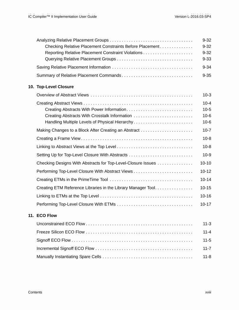
Analyzing Relative Placement Groups . . . . . . . . . . . . . . . . . . . . . . . . . . . . . . . . . . . 9-32
Checking Relative Placement Constraints Before Placement . . . . . . . . . . . . . . 9-32
Reporting Relative Placement Constraint Violations . . . . . . . . . . . . . . . . . . . . . 9-32
Querying Relative Placement Groups . . . . . . . . . . . . . . . . . . . . . . . . . . . . . . . . 9-33
Saving Relative Placement Information . . . . . . . . . . . . . . . . . . . . . . . . . . . . . . . . . . 9-34
Summary of Relative Placement Commands . . . . . . . . . . . . . . . . . . . . . . . . . . . . . . 9-35
10. Top-Level Closure
Overview of Abstract Views . . . . . . . . . . . . . . . . . . . . . . . . . . . . . . . . . . . . . . . . . . . 10-3
Creating Abstract Views . . . . . . . . . . . . . . . . . . . . . . . . . . . . . . . . . . . . . . . . . . . . . . 10-4
Creating Abstracts With Power Information. . . . . . . . . . . . . . . . . . . . . . . . . . . . 10-5
Creating Abstracts With Crosstalk Information . . . . . . . . . . . . . . . . . . . . . . . . . 10-6
Handling Multiple Levels of Physical Hierarchy . . . . . . . . . . . . . . . . . . . . . . . . . 10-6
Making Changes to a Block After Creating an Abstract . . . . . . . . . . . . . . . . . . . . . . 10-7
Creating a Frame View . . . . . . . . . . . . . . . . . . . . . . . . . . . . . . . . . . . . . . . . . . . . . . . 10-8
Linking to Abstract Views at the Top Level . . . . . . . . . . . . . . . . . . . . . . . . . . . . . . . . 10-8
Setting Up for Top-Level Closure With Abstracts . . . . . . . . . . . . . . . . . . . . . . . . . . . 10-9
Checking Designs With Abstracts for Top-Level-Closure Issues . . . . . . . . . . . . . . . 10-10
Performing Top-Level Closure With Abstract Views . . . . . . . . . . . . . . . . . . . . . . . . . 10-12
Creating ETMs in the PrimeTime Tool . . . . . . . . . . . . . . . . . . . . . . . . . . . . . . . . . . . 10-14
Creating ETM Reference Libraries in the Library Manager Tool. . . . . . . . . . . . . . . . 10-15
Linking to ETMs at the Top Level . . . . . . . . . . . . . . . . . . . . . . . . . . . . . . . . . . . . . . . 10-16
Performing Top-Level Closure With ETMs . . . . . . . . . . . . . . . . . . . . . . . . . . . . . . . . 10-17
11. ECO Flow
Unconstrained ECO Flow . . . . . . . . . . . . . . . . . . . . . . . . . . . . . . . . . . . . . . . . . . . . . 11-3
Freeze Silicon ECO Flow . . . . . . . . . . . . . . . . . . . . . . . . . . . . . . . . . . . . . . . . . . . . . 11-4
Signoff ECO Flow . . . . . . . . . . . . . . . . . . . . . . . . . . . . . . . . . . . . . . . . . . . . . . . . . . . 11-5
Incremental Signoff ECO Flow . . . . . . . . . . . . . . . . . . . . . . . . . . . . . . . . . . . . . . . . . 11-7
Manually Instantiating Spare Cells . . . . . . . . . . . . . . . . . . . . . . . . . . . . . . . . . . . . . . 11-8
Contents xviii

IC Compiler™ II Implementation User Guide Version L-2016.03-SP4
Automatically Adding Spare Cells . . . . . . . . . . . . . . . . . . . . . . . . . . . . . . . . . . . . . . . 11-10
Adding Programmable Spare Cells. . . . . . . . . . . . . . . . . . . . . . . . . . . . . . . . . . . . . . 11-11
Making ECO Changes Using the eco_netlist Command . . . . . . . . . . . . . . . . . . . . . 11-12
Comparing Netlist Differences Across Physical Hierarchy . . . . . . . . . . . . . . . . 11-13
Making ECO Changes Using Netlist Editing Commands . . . . . . . . . . . . . . . . . . . . . 11-15
Using Netlist Editing Commands in the Freeze Silicon Mode . . . . . . . . . . . . . . 11-16
Making Netlist Edits on Modules . . . . . . . . . . . . . . . . . . . . . . . . . . . . . . . . . . . . 11-16
Reverting Sized Cells . . . . . . . . . . . . . . . . . . . . . . . . . . . . . . . . . . . . . . . . . . . . 11-16
Placing ECO Cells . . . . . . . . . . . . . . . . . . . . . . . . . . . . . . . . . . . . . . . . . . . . . . . . . . 11-17
Controlling Placement When Using the place_eco_cells Command. . . . . . . . . 11-18
Controlling Legalization When Using the place_eco_cells Command. . . . . . . . 11-19
Placing and Mapping ECO Cells to Spare Cells . . . . . . . . . . . . . . . . . . . . . . . . . . . . 11-21
Mapping ECO Cells to Specific Spare Cells . . . . . . . . . . . . . . . . . . . . . . . . . . . 11-21
Updating Supply Nets for ECO Cells . . . . . . . . . . . . . . . . . . . . . . . . . . . . . . . . . . . . 11-22
Performing ECO Routing . . . . . . . . . . . . . . . . . . . . . . . . . . . . . . . . . . . . . . . . . . . . . 11-22
Adding Buffers on Routed Nets . . . . . . . . . . . . . . . . . . . . . . . . . . . . . . . . . . . . . . . . 11-23
Optimizing the Fanout of a Net . . . . . . . . . . . . . . . . . . . . . . . . . . . . . . . . . . . . . . . . . 11-26
Recording the Changes Made to a Layout . . . . . . . . . . . . . . . . . . . . . . . . . . . . . . . . 11-27
Chapter 1: Contents1-xixContents xix

IC Compiler™ II Implementation User Guide L-2016.03-SP4IC Compiler™ II Implementation User Guide Version L-2016.03-SP4
Contents xx

Preface
This preface includes the following sections:
• About This User Guide
• Customer Support
xxi

IC Compiler™ II Implementation User Guide L-2016.03-SP4IC Compiler™ II Implementation User Guide Version L-2016.03-SP4
About This User Guide
The Synopsys IC Compiler II tool provides a complete netlist-to-GDSII design solution, which combines proprietary design planning, physical synthesis, clock tree synthesis, and routing for logical and physical design implementations throughout the design flow.
This guide describes the IC Compiler II implementation and integration flow. For more information about the IC Compiler II tool, see the following companion volumes:
• IC Compiler II Library Preparation User Guide
• IC Compiler II Design Planning User Guide
• IC Compiler II Data Model User Guide
• IC Compiler II Timing Analysis User Guide
• IC Compiler II Graphical User Interface User Guide
Audience
This user guide is for design engineers who use the IC Compiler II tool to implement designs.
To use the IC Compiler II tool, you need to be skilled in physical design and synthesis and be familiar with the following:
• Physical design principles
• The Linux or UNIX operating system
• The tool command language (Tcl)
Related Publications
For additional information about the IC Compiler II tool, see the documentation on the Synopsys SolvNet® online support site at the following address:
https://solvnet.synopsys.com/DocsOnWeb
You might also want to see the documentation for the following related Synopsys products:
• Design Compiler®
• IC Validator
• PrimeTime® Suite
PrefaceAbout This User Guide xxii

IC Compiler™ II Implementation User Guide Version L-2016.03-SP4
Release Notes
Information about new features, enhancements, changes, known limitations, and resolved Synopsys Technical Action Requests (STARs) is available in the IC Compiler II Release Notes on the SolvNet site.
To see the IC Compiler II Release Notes,
1. Go to the SolvNet Download Center located at the following address:
https://solvnet.synopsys.com/DownloadCenter
2. Select IC Compiler II, and then select a release in the list that appears.
Conventions
The following conventions are used in Synopsys documentation.
Convention Description
Courier Indicates syntax, such as write_file.
Courier italic Indicates a user-defined value in syntax, such as write_file design_list.
Courier bold Indicates user input—text you type verbatim—in examples, such asprompt> write_file top
[ ] Denotes optional arguments in syntax, such as write_file [-format fmt]
... Indicates that arguments can be repeated as many times as needed, such as pin1 pin2 ... pinN.
| Indicates a choice among alternatives, such as low | medium | high
Ctrl+C Indicates a keyboard combination, such as holding down the Ctrl key and pressing C.
\ Indicates a continuation of a command line.
/ Indicates levels of directory structure.
Edit > Copy Indicates a path to a menu command, such as opening the Edit menu and choosing Copy.
Chapter 1: PrefaceAbout This User Guide 1-xxiiiPrefaceAbout This User Guide xxiii

IC Compiler™ II Implementation User Guide L-2016.03-SP4IC Compiler™ II Implementation User Guide Version L-2016.03-SP4
Customer Support
Customer support is available through SolvNet online customer support and through contacting the Synopsys Technical Support Center.
Accessing SolvNet
The SolvNet site includes a knowledge base of technical articles and answers to frequently asked questions about Synopsys tools. The SolvNet site also gives you access to a wide range of Synopsys online services including software downloads, documentation, and technical support.
To access the SolvNet site, go to the following address:
https://solvnet.synopsys.com
If prompted, enter your user name and password. If you do not have a Synopsys user name and password, follow the instructions to sign up for an account.
If you need help using the SolvNet site, click HELP in the top-right menu bar.
Contacting the Synopsys Technical Support Center
If you have problems, questions, or suggestions, you can contact the Synopsys Technical Support Center in the following ways:
• Open a support case to your local support center online by signing in to the SolvNet site at https://solvnet.synopsys.com, clicking Support, and then clicking “Open A Support Case.”
• Send an e-mail message to your local support center.
❍ E-mail [email protected] from within North America.
❍ Find other local support center e-mail addresses at
http://www.synopsys.com/Support/GlobalSupportCenters/Pages
• Telephone your local support center.
❍ Call (800) 245-8005 from within North America.
❍ Find other local support center telephone numbers at
http://www.synopsys.com/Support/GlobalSupportCenters/Pages
PrefaceCustomer Support xxiv

1Working With the IC Compiler II Tool 1
The IC Compiler II tool supports the following functionality for the flat flow:
• Extraction and timing analysis
• Placement and optimization, including relative placement
• Clock tree synthesis
• Routing
• Chip finishing
• Top-level closure for hierarchical designs
• Engineering change orders (ECO)
• Reporting
• ASCII output interfaces
It takes as input a Verilog gate-level netlist, a detailed floorplan in Design Exchange Format (DEF), timing constraints, physical and timing libraries, and foundry-process data. It generates as output a Verilog gate-level netlist, a DEF file of placed netlist data, and timing constraints.
1-1

IC Compiler™ II Implementation User Guide L-2016.03-SP4IC Compiler™ II Implementation User Guide Version L-2016.03-SP4
The following topics describe how to use the IC Compiler II tool:
• Methodology Overview
• IC Compiler II Concepts
• User Interfaces
• Entering icc2_shell Commands
• Using Application Options
• Using Variables
• Viewing Man Pages
• Using Tcl Scripts
• Using Setup Files
• Using the Command Log File
For information about working with design data in the IC Compiler II tool, see the IC Compiler II Data Model User Guide.
Chapter 1: Working With the IC Compiler II Tool1-2

IC Compiler™ II Implementation User Guide Version L-2016.03-SP4
Methodology Overview
Figure 1-1 shows the high-level design flow using the IC Compiler II tool.
Figure 1-1 High-Level Design Flow
To run the IC Compiler II design flow,
1. Set up the libraries and prepare the design data, as described in Preparing the Design.
2. Perform design planning and power planning.
When you perform design planning and power planning, you create a floorplan to determine the size of the design, create the boundary and core area, create site rows for the placement of standard cells, set up the I/O pads, and create a power plan.
For more information about design planning and power planning, see the IC Compiler II Design Planning User Guide.
3. Perform placement and optimization.
To perform placement and optimization, use the place_opt command.
Chapter 1: Working With the IC Compiler II ToolMethodology Overview 1-3Chapter 1: Working With the IC Compiler II ToolMethodology Overview 1-3

IC Compiler™ II Implementation User Guide L-2016.03-SP4IC Compiler™ II Implementation User Guide Version L-2016.03-SP4
The place_opt command addresses and resolves timing closure for your design. This iterative process uses enhanced placement and synthesis technologies to generate legalized placement for leaf cells and an optimized design. You can supplement this functionality by optimizing for power, recovering area for placement, minimizing congestion, and minimizing timing and design rule violations.
For more information about placement and optimization, see Placement and Optimization.
4. Perform clock tree synthesis and optimization.
To perform clock tree synthesis and optimization, use the clock_opt command.
IC Compiler II clock tree synthesis and embedded optimization solve complicated clock tree synthesis problems, such as blockage avoidance and the correlation between preroute and postroute data. Clock tree optimization improves both clock skew and clock insertion delay by performing buffer sizing, buffer relocation, gate sizing, gate relocation, level adjustment, reconfiguration, delay insertion, dummy load insertion, and balancing of interclock delays.
For more information about clock tree synthesis and optimization, see Clock Tree Synthesis.
5. Perform routing and postroute optimization, as described in Routing and Postroute Optimization.
The IC Compiler II tool uses Zroute to perform global routing, track assignment, detail routing, topological optimization, and engineering change order (ECO) routing. To perform postroute optimization, use the route_opt command. For most designs, the default postroute optimization setup produces optimal results. If necessary, you can supplement this functionality by optimizing routing patterns and reducing crosstalk or by customizing the routing and postroute optimization functions for special needs.
6. Perform chip finishing and design for manufacturing tasks, as described in Chip Finishing and Design for Manufacturing.
The IC Compiler II tool provides chip finishing and design for manufacturing and design for yield capabilities that you can apply throughout the various stages of the design flow to address process design issues encountered during chip manufacturing.
7. Save the design.
Chapter 1: Working With the IC Compiler II ToolMethodology Overview 1-4

IC Compiler™ II Implementation User Guide Version L-2016.03-SP4
IC Compiler II Concepts
This topic introduces the following concepts used in the IC Compiler II tool:
• Power Intent Concepts
• Multiple-Patterning Concepts
Power Intent Concepts
The IC Compiler II tool uses the Unified Power Format (UPF) to specify the power intent for multivoltage designs. This topic provides an overview of the UPF concepts and the supported UPF flows. For information about using UPF to specify the power intent, see the “Power Intent Specification” chapter in the Synopsys Multivoltage Flow User Guide.
UPF Concepts
The UPF language establishes a set of commands used to specify the low-power design intent for electronic systems. Using UPF commands, you can specify the supply network, switches, isolation, retention, and other aspects relevant to power management of a chip design. The same set of low-power design specification commands is to be used throughout the design, analysis, verification, and implementation flow. Synopsys tools are designed to follow the official UPF standard.
The UPF language provides a way to specify the power requirements of a design, but without specifying explicitly how those requirements are implemented. The language specifies how to create a power supply network for each design element, the behavior of supply nets with respect to each other, and how the logic functionality is extended to support dynamic power switching to design elements. It does not contain any placement or routing information.
In the UPF language, a power domain is a defined group of elements in the logic hierarchy that share a common set of power supply needs. By default, all logic elements in a power domain use the same primary supply and primary ground. Other power supplies can optionally be defined for a power domain as well. A power domain is typically implemented as a contiguous voltage area in the physical chip layout, although this is not a requirement of the language.
Each power domain has a scope and an extent. The scope is the level of logic hierarchy where the power domain exists. The extent is the set of logic elements that belong to the power domain and share the same power supply needs. In other words, the scope is the hierarchical level where the power domain exists, whereas the extent is what is contained within the power domain.
Chapter 1: Working With the IC Compiler II ToolIC Compiler II Concepts 1-5Chapter 1: Working With the IC Compiler II ToolIC Compiler II Concepts 1-5
IC Compiler™ II Implementation User Guide L-2016.03-SP4IC Compiler™ II Implementation User Guide Version L-2016.03-SP4
Each scope or hierarchical level in the design has supply nets and supply ports. A supply net is a conductor that carries a supply voltage or ground throughout a given power domain. A supply net that spans more than one power domain is said to be “reused” in multiple domains. A supply port is a power supply connection point between two adjacent levels of the design hierarchy, between parent and child blocks of the hierarchy. A supply net that crosses from one level of the design hierarchy to the next must pass through a supply port.
A power switch (or simply switch) is a device that turns on and turns off power for a supply net. A switch has an input supply net, an output supply net that can be switched on or off, and at least one input signal to control switching. The switch can optionally have multiple input control signals and one or more output acknowledge signals. A power state table lists the allowed combinations of voltage values and states of the power switches for all power domains in the design.
Where a logic signal leaves one power domain and enters another at a substantially different supply voltage, a level-shifter cell must be present to convert the signal from the voltage swing of the first domain to that of the second domain.
Where a logic signal leaves a power domain and enters a different power domain, an isolation cell must be present to generate a known logic value during shutdown. If the voltage levels of the two domains are substantially different, the interface cell must perform both level shifting when the domain is powered up and isolation when the domain is powered down. A cell that can perform both functions is called an enable level shifter.
In a power domain that has power switching, any registers that are to retain data during shutdown must be implemented as retention registers. A retention register has a separate, always-on supply net, sometimes called the backup supply, which keeps the data stable in while the primary supply of the domain is shut down.
UPF Flows
The IC Compiler II tool supports both the traditional UPF flow and the golden UPF flow. The golden UPF flow is an optional method of maintaining the UPF multivoltage power intent of the design. It uses the original “golden” UPF file throughout the synthesis, physical implementation, and verification steps, along with supplemental UPF files generated by the Design Compiler and IC Compiler II tools.
Chapter 1: Working With the IC Compiler II ToolIC Compiler II Concepts 1-6

IC Compiler™ II Implementation User Guide Version L-2016.03-SP4
Figure 1-2 compares the traditional UPF flow with the golden UPF flow.
Figure 1-2 UPF-Prime (Traditional) and Golden UPF Flows
The golden UPF flow maintains and uses the same, original “golden” UPF file throughout the flow. The Design Compiler and IC Compiler II tools write power intent changes into a separate “supplemental” UPF file. Downstream tools and verification tools use a combination of the golden UPF file and the supplemental UPF file, instead of a single UPF’ or UPF’’ file.
The golden UPF flow offers the following advantages:
• The golden UPF file remains unchanged throughout the flow, which keeps the form, structure, comment lines, and wildcard naming used in the UPF file as originally written.
• You can use tool-specific conditional statements to perform different tasks in different tools. Such statements are lost in the traditional UPF-prime flow.
Gate-level netlist
RTL UPF
Gate-level netlist
RTL
SupplementalUPF
Gate-level netlist
SupplementalUPF
Design CompilerPower Compiler
Design CompilerPower Compiler
IC Compiler II IC Compiler II
UPF-prime (traditional) flow Golden UPF flow
Gate-level netlistUPF’
UPF’’
Verification tools Verification tools
Golden UPF
Chapter 1: Working With the IC Compiler II ToolIC Compiler II Concepts 1-7Chapter 1: Working With the IC Compiler II ToolIC Compiler II Concepts 1-7

IC Compiler™ II Implementation User Guide L-2016.03-SP4IC Compiler™ II Implementation User Guide Version L-2016.03-SP4
• Changes to the power intent are easily tracked in the supplemental UPF file.
• You can optionally use the Verilog netlist to store all PG connectivity information, making connect_supply_net commands unnecessary in the UPF files. This can significantly simplify and reduce the overall size of the UPF files.
In the IC Compiler II tool, the load_upf command loads all UPF file types, including any mixture of UPF-prime, golden UPF, and supplemental UPF files. In the golden UPF flow, the load_upf command automatically identifies UPF commands as golden or supplemental based on the setting of the derived_upf variable in the UPF file. For details, see the man page for the load_upf command and “Preserving the Command Order in the UPF' File” in the Power Compiler User Guide.
For more information about using the golden UPF flow, see SolvNet article 1412864, “Golden UPF Flow Application Note.”
Multiple-Patterning Concepts
At the 20-nm process node and below, printing the required geometries is extremely difficult with the existing photolithography tools. To address this issue, a new technique, multiple patterning, is used to partition the layout mask into two or more separate masks, each of which has an increased manufacturing pitch to enable higher resolution and better printability. Figure 1-3 shows an example of double-patterning, where the layout mask is partitioned into two separate masks, MASK A and MASK B.
Figure 1-3 Double-Patterning Example
To use multiple patterning, you must be able to decompose the layout into two or more masks, each of which meets the multiple-patterning spacing requirements. A
Chapter 1: Working With the IC Compiler II ToolIC Compiler II Concepts 1-8

IC Compiler™ II Implementation User Guide Version L-2016.03-SP4
multiple-patterning violation occurs if your layout contains a region with an odd number of neighboring shapes where the distance between each pair of shapes is smaller than the multiple-patterning minimum spacing. This type of violation, which is called an odd cycle, is shown in Figure 1-4.
Figure 1-4 Odd-Cycle Violation
If the spacing between any pair in the loop is greater than the multiple-patterning minimum spacing, no violation occurs and the layout can be decomposed. For example, in Figure 1-5, if the spacing, x, between segments B and C is greater than the multiple-patterning minimum spacing, there is no odd cycle and the layout can be decomposed.
Figure 1-5 No Odd-Cycle Violation
The IC Compiler II tool ensures that the generated layout is conducive to double patterning by considering the multiple-patterning spacing requirements during placement and routing and preventing odd cycles.
In general, double patterning is performed only on the bottom (lowest) metal layers, which are referred to as multiple-patterning layers. The metal shapes on the multiple-patterning layers must meet the multiple-patterning spacing requirements, whether they are routing shapes or metal within the standard cells and macros. The metal shapes on other layers do not need to meet the stricter multiple-patterning spacing requirements.
Layout with an odd cycle Spacing violation prevents decomposition
Layout with no odd cycle Layout can be decomposed
Chapter 1: Working With the IC Compiler II ToolIC Compiler II Concepts 1-9Chapter 1: Working With the IC Compiler II ToolIC Compiler II Concepts 1-9

IC Compiler™ II Implementation User Guide L-2016.03-SP4IC Compiler™ II Implementation User Guide Version L-2016.03-SP4
Multiple-patterning considerations affect all parts of the place and route flow. Depending on your standard cell library, you follow either an uncolored or precolored multiple-patterning flow.
• You use the uncolored flow if the cells in your standard library have sufficient spacing to the cell boundaries to ensure that multiple-patterning violations do not occur during placement. This type of library is referred to as a correct-by-construction library; most multiple-patterning libraries are correct-by-construction libraries.
In the uncolored flow, the tool determines the appropriate mask settings for the pins and net shapes.
• You use the precolored flow if the cells in your standard library have assigned masks on the metal shapes inside the cells. These assigned masks are often referred to as colors and this type of library is referred to as a precolored library.
In the precolored flow, the tool must consider these mask assignments to ensure that multiple-patterning violations do not occur during placement. The tool also uses the mask assignments to determine the appropriate mask settings for the pins and net shapes.
The mask assignments are represented as mask constraints in the IC Compiler II tool. You must ensure that the mask constraints are properly set before starting place and route. For information about the mask constraints, see Mask Constraints.
Mask Constraints
Mask constraints indicate the mask requirements for the metal shapes of the physical pins and nets in a block that uses multiple-patterning technology. These mask requirements drive placement and routing to ensure that the resulting layout is multiple-patterning compliant.
Note: Mask constraints are used only for the precolored flow; they are not necessary in the uncolored flow.
You can set mask constraints on timing-critical nets (net shapes, routing rules, and routing blockages) and vias. For nets, the mask constraint is defined in the mask_constraint attribute. For vias, the mask constraints are defined in the lower_mask, upper_mask, and cut_mask attributes. Table 1-1 shows the supported values for these attributes.
Chapter 1: Working With the IC Compiler II ToolIC Compiler II Concepts 1-10

IC Compiler™ II Implementation User Guide Version L-2016.03-SP4
User Interfaces
The IC Compiler II tool operates in the X windows environment on UNIX or Linux. It provides a flexible working environment with both a shell command-line interface and a graphical user interface (GUI). The shell command-line interface, icc2_shell, is always available during a IC Compiler II session. You can start or exit a session in either icc2_shell or the GUI, and you can open or close the GUI at any time during a session.
The IC Compiler II tool uses the tool command language (Tcl), which is used in many applications in the EDA industry. Using Tcl, you can extend the icc2_shell command language by writing reusable procedures and scripts (see the Using Tcl With Synopsys Tools manual).
The following topics describe how to start and exit the tool using the command-line interface.
• Starting the Command-Line Interface
• Exiting the IC Compiler II Tool
For information about using the GUI, see the IC Compiler II Graphical User Interface User Guide.
Table 1-1 Mask Constraint Values
Attribute value Description
same_mask This constraint means that the mask color is not yet been determined. Shapes with this attribute must be at least the multiple-patterning minimum spacing distance from any other colored metal shape.
mask_one This constraint means that the shape has the mask1 color. Shapes with this attribute must be at least the multiple-patterning minimum spacing distance from other mask1-colored metal shapes.
mask_two This constraint means that the shape has the mask2 color. Shapes with this attribute must be at least the multiple-patterning minimum spacing distance from other mask2-colored metal shapes.
mask_three This constraint means that the shape has the mask3 color. Shapes with this attribute must be at least the multiple-patterning minimum spacing distance from other mask3-colored metal shapes.
any_mask This constraint means that the shape is not colored. Shapes with this attribute must be at least the standard minimum spacing distance from other metal shapes; the multiple-patterning minimum spacing rules do not apply to these shapes.
Chapter 1: Working With the IC Compiler II ToolUser Interfaces 1-11Chapter 1: Working With the IC Compiler II ToolUser Interfaces 1-11

IC Compiler™ II Implementation User Guide L-2016.03-SP4IC Compiler™ II Implementation User Guide Version L-2016.03-SP4
Starting the Command-Line Interface
The icc2_shell command-line interface is a text-only environment in which you enter commands at the command-line prompt. It is typically used for scripts, batch mode, and push-button operations.
To start icc2_shell,
1. Make sure the path to the bin directory is included in your $PATH variable.
2. Enter the icc2_shell command in a UNIX or Linux shell.
% icc2_shell
You can include other options on the command line when you start icc2_shell. For example, you can use
• -f script_file_name to execute a script
• -x command to execute an icc2_shell command
• -output_log_file file_name to create a log file of your session
• -h to display a list of the available options (without starting icc2_shell)
At startup, icc2_shell performs the following tasks:
1. Creates a command log file.
2. Reads and executes the setup files.
3. Executes any script files or commands specified by the -f and -x options, respectively, on the command line.
4. Displays the program header and icc2_shell> prompt in the shell in which you started icc2_shell.
See Also
• Using the Command Log File
• Using Setup Files
• Using Tcl Scripts
Chapter 1: Working With the IC Compiler II ToolUser Interfaces 1-12

IC Compiler™ II Implementation User Guide Version L-2016.03-SP4
Exiting the IC Compiler II Tool
You can end the session and exit the IC Compiler II tool at any time. To exit the tool, use the exit or quit command.
Note: When you exit the tool from the command line, the tool exits without saving the open blocks.
Entering icc2_shell Commands
You interact with the IC Compiler II tool by using icc2_shell commands, which are based on the tool command language (Tcl) and include certain command extensions needed to implement specific IC Compiler II functionality. The IC Compiler II command language provides capabilities similar to UNIX command shells, including variables, conditional execution of commands, and control flow commands. You can
• Enter individual commands interactively at the icc2_shell> prompt in icc2_shell
• Enter individual commands interactively on the console command line in the GUI
• Run one or more Tcl scripts, which are text files that contain icc2_shell commands (see Using Tcl Scripts)
When entering a command, an option, or a file name, you can minimize your typing by pressing the Tab key when you have typed enough characters to specify a unique name; the IC Compiler II tool completes the remaining characters. If the characters you typed could be used for more than one name, the IC Compiler II tool lists the qualifying names, from which you can select by using the arrow keys and the Enter key.
If you need to reuse a command from the output for a command-line interface, you can copy and paste the portion by selecting it, moving the pointer to the icc2_shell command line, and clicking with the middle mouse button.
When you run a command, the IC Compiler II tool echoes the command output (including processing messages and any warnings or error messages) in icc2_shell and, if the GUI is open, in the console log view. By default, the tool does not use page mode, so the output might scroll. To enable page mode, set the sh_enable_page_mode variable to true.
Chapter 1: Working With the IC Compiler II ToolEntering icc2_shell Commands 1-13Chapter 1: Working With the IC Compiler II ToolEntering icc2_shell Commands 1-13

IC Compiler™ II Implementation User Guide L-2016.03-SP4IC Compiler™ II Implementation User Guide Version L-2016.03-SP4
Interrupting or Terminating Command Processing
If you enter the wrong options for a command or enter the wrong command, you can interrupt command processing and remain in icc2_shell. To interrupt or terminate a command, press Ctrl+C.
Some commands and processes cannot be interrupted. To stop these commands or processes, you must terminate icc2_shell at the system level. When you terminate a process or the shell, no data is saved.
When you use Ctrl+C, keep the following points in mind:
• If a script file is being processed and you interrupt one of its commands, the script processing is interrupted and no further script commands are processed.
• If you press Ctrl+C three times before a command responds to your interrupt, icc2_shell is interrupted and exits with this message:
Information: Process terminated by interrupt.
Getting Information About Commands
The following online information resources are available while you are using the IC Compiler II tool:
• Command help, which is information about an icc2_shell command
• Man pages
See Also
• Viewing Man Pages
Chapter 1: Working With the IC Compiler II ToolEntering icc2_shell Commands 1-14

IC Compiler™ II Implementation User Guide Version L-2016.03-SP4
Displaying Command Help
Command help consists of either a brief description of an icc2_shell command or a list of the options and arguments supported by an icc2_shell command.
• To display a brief description of an icc2_shell command, enter the help command followed by the command name. For example, to display a brief description of the report_timing command, use the following command:
icc2_shell> help report_timing
• To display the options supported by an icc2_shell command, enter the command name with the -help option on the icc2_shell command line. For example, to see the options supported by the report_timing command, use the following command:
icc2_shell> report_timing -help
Using Application Options
The IC Compiler II tool uses application options to control the tool behavior. Application options use the following naming convention:
category[.subcategory].option_name
where category is the name of the engine affected by the application option. Some application option categories have subcategories to further refine the area affected by the application option.
Application options have either a global scope or a block scope.
• Block-scoped application options apply only to the block on which they are set. They are saved in the design library and are persistent across tool sessions.
• Global-scoped application options apply to all blocks, but only within the current session. They are not saved in the design library; you must specify them in each icc2_shell session. You might want to consider adding the global settings to your .synopsys_icc2.setup file.
To get a list of available application options, use the get_app_options command. By default, this command lists all application options. To restrict the reported application options, provide a pattern string as an argument to the command.
For example, to list all available application options, use the following command:
icc2_shell> get_app_options
To list all available timer application options, use the following command:
icc2_shell> get_app_options timer.*
Chapter 1: Working With the IC Compiler II ToolUsing Application Options 1-15Chapter 1: Working With the IC Compiler II ToolUsing Application Options 1-15

IC Compiler™ II Implementation User Guide L-2016.03-SP4IC Compiler™ II Implementation User Guide Version L-2016.03-SP4
For detailed information about application options, see “Application Options” in the IC Compiler II Data Model User Guide.
See Also
• Using Setup Files
Using Variables
In general, the IC Compiler II tool modifies default behavior by using application options rather than application variables; however it does support user-defined Tcl variables, as well as a minimal number of application variables, such as the search_path variable.
See Also
• Defining the Search Path
Viewing Man Pages
To display the man page for an icc2_shell command or application variable, enter the man command followed by the command or variable name. For example, to see the man page for the report_timing command, use the following command:
icc2_shell> man report_timing
To display the man page for an icc2_shell application option, enter the man command followed by the option name. You can also view the following types of summary pages for application options:
• Category summaries
To view a man page the summarizes all of the application options for a specific category, enter the man command followed by category_options. For example, to see the man page that summarizes all timer application options, use the following command:
icc2_shell> man timer_options
• Subcategory summaries
To view a man page the summarizes all of the application options for a specific subcategory, enter the man command followed by category.subcategory_options. For example, to see the man page that summarizes all common route application options, use the following command:
icc2_shell> man route.common_options
Chapter 1: Working With the IC Compiler II ToolUsing Variables 1-16

IC Compiler™ II Implementation User Guide Version L-2016.03-SP4
• Command summaries
To view a man page the summarizes all of the application options for a specific command, enter the man command followed by command_options. For example, to see the man page that summarizes all application options that affect the report_timing command, use the following command:
icc2_shell> man report_timing_options
If you enter the man command on the icc2_shell command line, the man page is displayed in the IC Compiler II shell and in the console log view if the GUI is open. If you enter this command on the console command line in the GUI, the man page is displayed in the GUI man page viewer.
Using Tcl Scripts
You can use Tcl scripts to accomplish routine, repetitive, or complex tasks. You create a command script file by placing a sequence of icc2_shell commands in a text file. Any icc2_shell command can be executed within a script file.
In Tcl, a pound sign (#) at the beginning of a line denotes a comment. For example,
# This is a comment
For more information about writing scripts and script files, see the Using Tcl With Synopsys Tools manual.
Use one of the following methods to run a Tcl script:
• Use the -f option with the icc2_shell command when you start the IC Compiler II tool.
• Use the source command from the icc2_shell command line.
• Choose File > Execute Script in the GUI.
If an error occurs when running a command, the IC Compiler II tool raises the TCL_ERROR condition, which immediately stops the script execution. To tolerate errors and allow the script to continue executing, either
• Check for TCL_ERROR error conditions with the Tcl catch command on the commands that might generate errors.
• Set the sh_continue_on_error variable to true in the script file.
See Also
• Starting the Command-Line Interface
Chapter 1: Working With the IC Compiler II ToolUsing Tcl Scripts 1-17Chapter 1: Working With the IC Compiler II ToolUsing Tcl Scripts 1-17

IC Compiler™ II Implementation User Guide L-2016.03-SP4IC Compiler™ II Implementation User Guide Version L-2016.03-SP4
Using Setup Files
When you start the IC Compiler II tool, it automatically executes the commands in the .synopsys_icc2.setup file.
The tool looks for this file both in your home directory and in the project directory (the current working directory in which you start the IC Compiler II tool). The file is read in the following order:
1. The .synopsys_icc2.setup file in your home directory
2. The .synopsys_icc2.setup file in the project directory
The setup files can contain commands that perform basic tasks, such as initializing application options and setting GUI options. You can add commands and Tcl procedures to the setup files in your home and project directories. For example,
• To set application options that define your IC Compiler II working environment, create setup files in your home directory.
• To set project- or block-specific application options that affect the processing of a block, create a setup file in the design directory.
See Also
• User Interfaces
• Using Application Options
• Using Variables
• Using Tcl Scripts
Chapter 1: Working With the IC Compiler II ToolUsing Setup Files 1-18

IC Compiler™ II Implementation User Guide Version L-2016.03-SP4
Using the Command Log File
The command log file records the icc2_shell commands processed by the IC Compiler II tool, including setup file commands and application option settings. By default, the IC Compiler II tool writes the command log to a file named icc2_command.log in the directory from which you invoked icc2_shell.
You can change the name of the command log file by setting the sh_command_log_file variable in your .synopsys_icc2.setup file. You should make any changes to this variable before you start the IC Compiler II tool. If your user-defined or project-specific setup file does not contain this variable, the IC Compiler II tool automatically creates the icc2_command.log file.
Each IC Compiler II session overwrites the command log file. To save a command log file, move it or rename it. You can use the command log file to
• Produce a script for a particular implementation strategy
• Record the physical implementation process
• Document any problems you are having
Chapter 1: Working With the IC Compiler II ToolUsing the Command Log File 1-19Chapter 1: Working With the IC Compiler II ToolUsing the Command Log File 1-19

IC Compiler™ II Implementation User Guide L-2016.03-SP4IC Compiler™ II Implementation User Guide Version L-2016.03-SP4
Chapter 1: Working With the IC Compiler II ToolUsing the Command Log File 1-20

2Preparing the Design 2
The IC Compiler II tool uses a design library to store your design and its associated library information. This topic describes how to create a design library and how to prepare and save your design.
These steps are explained in the following topics:
• Defining the Search Path
• Working With Design Libraries
• Working With Designs
• Annotating the Floorplan Information
• Annotating the Scan Chain Information
• Loading the Power Intent
• Preparing for Timing Analysis
• Preparing the Power Network
• Preparing for Optimization
• Preparing for Percentage Low-Threshold-Voltage Optimization
• Annotating the Switching Activity
2-1

IC Compiler™ II Implementation User Guide L-2016.03-SP4IC Compiler™ II Implementation User Guide Version L-2016.03-SP4
• Specifying the Routing Resources
• Enabling Multicore Processing
Chapter 2: Preparing the Design2-2

IC Compiler™ II Implementation User Guide Version L-2016.03-SP4
Defining the Search Path
The IC Compiler II tool uses a search path to look for files that are specified with a relative path or with no path.
To specify the search path, use the set_app_var command to set the search_path application variable to the list of directories, in order, in which to look for files. When the tool looks for a file, it starts searching in the leftmost directory specified in the search_path variable and uses the first matching file it finds.
You can also use the Tcl lappend command to add your directories to the default search path, which is the directory from which you invoked the tool. For example,
icc2_shell> lappend search_path ./mylibdir
Working With Design Libraries
All of the information about a design, including the associated technology information and the reference libraries, is stored in a design library. In addition to the technology and reference library information, a design library contains various versions of the designs stored in the design library. A version of a design is referred to as a block. The block name can be the same as or different than the top module name of the design. For example, for a design with a top module named my_design, you could have blocks named my_design_preplace, my_design_postplace, and my_design_postcts.
For each block, the design library can contain one or more of the following views:
• Design view
The design view contains the layout information for the block.
• Frame view
The frame view contains the place and route information for the block.
• Outline view
The outline view is used for floorplan creation for very large hierarchical blocks. It contains the hierarchy information, but no leaf cells or nets. For information about creating and using the outline view, see the IC Compiler II Design Planning User Guide.
• Abstract view
The abstract view is a lightweight representation of the block that contains only the information needed to perform placement, timing, and other tasks. For information about creating and using the abstract view, see the IC Compiler II Design Planning User Guide.
Chapter 2: Preparing the DesignDefining the Search Path 2-3Chapter 2: Preparing the DesignDefining the Search Path 2-3

IC Compiler™ II Implementation User Guide L-2016.03-SP4IC Compiler™ II Implementation User Guide Version L-2016.03-SP4
Figure 2-1 shows a high-level view of the contents of a typical design library.
Figure 2-1 Design Library
The current library is the design library used by default by most library-related commands. If you open more than open design library, by default, the current library is the last one opened. You can also explicitly set the current library by using the current_lib command.
Use the following commands to work with design libraries:
• create_lib: Creates a design library
• open_lib: Opens an existing design library
• save_lib: Saves a design library
• close_lib: Closes a design library
For detailed information about working with design libraries, see the IC Compiler II Data Model User Guide.
Working With Designs
In most cases, when you work with a design in the IC Compiler II tool, you use the design view of one of its versions (blocks) from the design library. In this manual, the term block is used to refer to a specific design version in the design library, whether it is a top-level design or a subdesign, and the term design is used generically to refer to the design being processed. In both cases, unless otherwise specified, the term refers to the design view.
Chapter 2: Preparing the DesignWorking With Designs 2-4

IC Compiler™ II Implementation User Guide Version L-2016.03-SP4
The IC Compiler II tool reads designs in Verilog format. The Verilog netlist file is a structural or gate-level design in one file. To read a design into the IC Compiler II tool,
1. Create or open the design library associated with the design.
❍ If the design library does not yet exist, use the create_lib command to create it.
❍ If the design library already exists, use the open_lib command to open it.
2. Read the Verilog netlist files for the design by using the read_verilog command.
By default, when the tool reads the Verilog netlist files, it creates a block in the current design library and increments its open count. The tool determines the top-level module of the block by identifying the module that is not instantiated by any other modules in the specified Verilog files and uses the top-level module name as the block name.
The tool also creates a default power domain for the block. For multivoltage designs, this default power domain is replaced when you specify the power intent, as described in Loading the Power Intent.
Use the following commands to work with blocks:
• create_block: Creates a block
• open_block: Opens an existing block
• current_block: Sets or reports the current block
• save_block: Saves a block
• close_blocks: Closes a block
For detailed information about working with designs and blocks, see the IC Compiler II Data Model User Guide.
See Also
• Working With Design Libraries
Chapter 2: Preparing the DesignWorking With Designs 2-5Chapter 2: Preparing the DesignWorking With Designs 2-5

IC Compiler™ II Implementation User Guide L-2016.03-SP4IC Compiler™ II Implementation User Guide Version L-2016.03-SP4
Annotating the Floorplan Information
If a floorplan already exists for a block, use the read_def command to annotate the floorplan information on the block.
Reading DEF Files
To read the floorplan information from a DEF file, use the read_def command.
icc2_shell> read_def block.def
Note: When possible, use DEF v5.7 or later, as this version supports more types of physical objects and obstructions than previous versions.
By default, the read_def command
• Annotates the floorplan information onto the current block
To annotate the information onto a different block, use the -design option to specify the block name.
• Preserves the existing floorplan information
To remove the existing floorplan information before annotating the floorplan information from the DEF file, use the -no_incremental option.
• Ignores any objects in the DEF file that do not exist in the block, except for PG objects
To allow new non-PG objects to be created from the DEF file, use the -add_def_only_objects option to specify the types of objects to create. Specify one or more of the following keywords:
❍ cells
The tool creates the cells that exist only in the DEF file and connects their power and ground pins as defined in the DEF file; it does not connect the signal, clock, or tie pins even if these connections are defined in the DEF file. The tool also does not create new hierarchical cells; any hierarchy specified in the DEF file must already exist in the block.
❍ nets
The tool creates the signal, clock, and tie nets that exist only in the DEF file and connects them to the ports specified in the DEF PINS section; it does not connect the nets to any other ports or pins in the netlist even if these connections are defined in the DEF file. The tool does not create new hierarchical nets; any hierarchy specified in the DEF file must already exist in the block.
Chapter 2: Preparing the DesignAnnotating the Floorplan Information 2-6

IC Compiler™ II Implementation User Guide Version L-2016.03-SP4
❍ ports
The tool creates the signal, clock, and tie ports that exist only in the DEF file and connects them to the nets specified in the DEF PINS section.
❍ all
The tool creates the non-PG cells, nets, and ports that exist only in the DEF file, as if you had specified cells, nets, and ports.
Fixing Site Name Mismatches
If the site names used in the DEF file do not match the site names defined in the technology file, use the -convert_sites option to specify the site name mapping. For example, if the DEF file uses a site named CORE, but the technology file defines only a site named unit, use the following command to convert the site names when reading the DEF file:
icc2_shell> read_def -convert_sites { {CORE unit} } block.def
Validating DEF Files
To analyze the input DEF files before annotating the floorplan information on the block, enable check-only mode by using the -syntax_only option. The check-only mode provides diagnostic information about the correctness and integrity of the DEF file. The check-only mode does not annotate any floorplan information onto the block.
icc2_shell> read_def -syntax_only block.def
Inheriting Port Locations
If the DEF file or floorplan does not contain port-location information, the IC Compiler II tool inherits the port locations from the locations of the pad cells. To ensure that this inheritance works on your block, the I/O cells and the pad pins of these I/O must have the proper attributes. If your reference libraries do not have these attributes, you can use the set_attribute command to set them.
To identify a library cell as a pad cell, set the pad_cell attribute for the library cell to true. For example, to identify the library cells named IOCell in all reference libraries as pad cells, use the following command:
icc2_shell> set_attribute -objects [get_lib_cells */IOCell] \-name pad_cell -value true
To identify a library cell pin as a pad pin, set the is_pad attribute for the library cell pin to true. For example, to identify the library cell pins named PADpin on all cells named IOCell in all reference libraries as pad pins, use the following command:
icc2_shell> set_attribute -objects [get_lib_pins */IOCell/PADpin] \-name is_pad -value true
Chapter 2: Preparing the DesignAnnotating the Floorplan Information 2-7Chapter 2: Preparing the DesignAnnotating the Floorplan Information 2-7

IC Compiler™ II Implementation User Guide L-2016.03-SP4IC Compiler™ II Implementation User Guide Version L-2016.03-SP4
Note: When you refer to the library in the get_lib_cells command, you must use the name of the reference library rather than the name of the logic (.db) library. To search in all libraries, use an asterisk (*) for the library name.
Annotating the Scan Chain Information
The IC Compiler II tool gets the scan chain information from a SCANDEF file, which specifies the scan chain components and their pins used for the scan path, along with reordering constraints. To get the best quality of results (QoR) for scan designs and enable repartitioning and reordering of the scan chains, you must annotate the scan chain information by loading the SCANDEF file.
For best results, you should use DFT Compiler for DFT insertion and Design Compiler topographical mode to generate the SCANDEF file. For more information about DFT insertion, see the DFT Compiler, DFTMAX, and DFTMAX Ultra User Guide . For more information about generating the SCANDEF file, see the Design Compiler User Guide.
Loading a SCANDEF File
To load a SCANDEF file, use the read_def command.
icc2_shell> read_def ./myscan.def
Note: If you have previously annotated the scan chain information on the block and the SCANDEF data contains a chain with the same name as an existing scan chain, the existing chain definition is preserved.
Loading the Power Intent
To load the power intent for a multivoltage design,
1. Read the UPF file by using the load_upf command.
icc2_shell> load_upf block.upf
2. If you are using the golden UPF flow and have a name mapping file from Design Compiler, read the name mapping file by using the read_name_map command.
icc2_shell> read_name_map block.nmf
Chapter 2: Preparing the DesignAnnotating the Scan Chain Information 2-8

IC Compiler™ II Implementation User Guide Version L-2016.03-SP4
3. (Optional) Verify the UPF consistency and identify any PG conflicts among the netlist, floorplan, and power intent.
To verify the UPF consistency and identify PG conflicts, use the resolve_pg_nets -check_only command. This command identifies any issues and reports the changes that will be made to resolve these issues when you commit the power intent. If you prefer to resolve the issues differently, you can use manual editing commands to resolve the issues before running the commit_upf command.
4. Commit the power intent by using the commit_upf command.
icc2_shell> commit_upf
The commit_upf command performs global checks for UPF consistency; resolves PG conflicts among the netlist, floorplan, and UPF specification; and associates power strategies with existing multivoltage cells. For more information about associating power strategies with existing multivoltage cells, see Associating Power Strategies With Existing Multivoltage Cells.
After running the commit_upf command, use the report_mv_path command to report the associations made for the multivoltage cells. If the tool failed to associate any multivoltage cells, the report_mv_path command reports the causes for these failures.
You must successfully commit the power intent before you continue with the design flow.
Note: After successfully running the commit_upf command, the tool issues an error message if you try to use additional UPF commands, except for the set_related_supply_net, connect_supply_net, set_design_attributes, set_port_attributes, find_objects, and set_scope commands. To modify the power intent after running the commit_upf command, you must remove the existing UPF specification by using the reset_upf command and then reload the power intent.
See Also
• Power Intent Concepts
Chapter 2: Preparing the DesignLoading the Power Intent 2-9Chapter 2: Preparing the DesignLoading the Power Intent 2-9

IC Compiler™ II Implementation User Guide L-2016.03-SP4IC Compiler™ II Implementation User Guide Version L-2016.03-SP4
Preparing for Timing Analysis
The IC Compiler II tool uses on-chip variation (OCV) mode to perform timing analysis, which models the effects of variation in operating conditions across the chip. This mode performs a conservative timing analysis that allows both minimum and maximum delays to apply to different paths at the same time. For a setup check, it uses maximum delays for the launch clock path and datapath and minimum delays for the capture clock path. For a hold check, it uses minimum delays for the launch clock path and datapath and maximum delays for the capture clock path.
A block might operate under several different conditions, such as different temperatures and voltages, and might operate in several different functional modes. For timing analysis, each set of conditions is represented by a corner and each functional mode is represented by a mode. A scenario is a combination of a corner and mode used to perform timing analysis and optimization. Before you start working with a block, you must define the modes, corners, and scenarios that are used for the block, as well as the delay calculation model and routing layers to use. The routing layer information you specify is used for RC estimation during timing analysis.
For detailed information about working with modes, corners, and scenarios, setting timing constraints and settings, and specifying parasitic information for RC estimation and extraction, see the IC Compiler II Timing Analysis User Guide. For detailed information about specifying routing layers, see Specifying the Routing Resources.
Preparing the Power Network
To learn about preparing the power network for physical implementation, see
• Creating Logical Power and Ground Connections
• Creating Floating Logical Supply Nets
• Verifying the Power Network Definition
Creating Logical Power and Ground Connections
After you read in the design, you must ensure that there are logical connections between the power and ground nets and the power, ground, and tie-off pins on the cells in your design. If your design does not already have these connections, use the connect_pg_net command to create them. This command creates the logical power and ground connections for leaf cells, hierarchical cells, and physical-only cells in both single-voltage and multivoltage designs.
Chapter 2: Preparing the DesignPreparing for Timing Analysis 2-10

IC Compiler™ II Implementation User Guide Version L-2016.03-SP4
Before creating the logical power and ground connections, you must resolve any PG conflicts among the netlist, floorplan, and UPF specification.
• For multivoltage designs, the conflicts are resolved when you commit the power intent, as described in Loading the Power Intent.
• For single-voltage designs, you must run the resolve_pg_nets command to resolve the conflicts. Note that the UPF specification for a single-voltage design is the default power domain that was generated by the read_verilog command.
The connect_pg_net command operates in two modes:
• Automatic
In automatic mode, the command derives all power and ground nets, power and ground pins, and connections from the UPF specification. If the supply nets do not exist, the tool creates them.
To create the logical power and ground connections in automatic mode, use the -automatic option with the connect_pg_net command. For example, to connect all power and ground pins based on the committed power intent, use the following command:
icc2_shell> connect_pg_net -automatic
• Manual
In manual mode, the command makes the connections that you specify. If a specified pin or port has an existing connection, the tool removes the existing connection and then creates the specified connection. The tool verifies that the connections match the power intent. If it finds a mismatch, the tool issues a warning but still creates the connection.
To create logical power and ground connections in manual mode, use the -net option to specify the power or ground net and specify the pins and ports to be connected to that net as an argument to the command. For example, to connect the VDD power net to all pins named vdd and the VSS ground net to all pins named vss, use the following commands:
icc2_shell> connect_pg_net -net VDD [get_pins */vdd]icc2_shell> connect_pg_net -net VSS [get_pins */vss]
Chapter 2: Preparing the DesignPreparing the Power Network 2-11Chapter 2: Preparing the DesignPreparing the Power Network 2-11

IC Compiler™ II Implementation User Guide L-2016.03-SP4IC Compiler™ II Implementation User Guide Version L-2016.03-SP4
Creating Floating Logical Supply Nets
A floating logical supply net is a power or ground net that is not connected to any logical pin or port in the block. For example, a power feedthrough net created during power planning is a floating supply net.
To create a floating supply net with the connect_pg_net command, use the following steps:
1. Specify the supply net type in the UPF file by using the supply_net_pg_type attribute, as shown in the following UPF file example:
…create_supply_net VDD……set_design_attribute -elements VDD -attribute supply_net_pg_type power…
2. Enable floating supply nets by setting the mv.pg.create_floating_pg application option to true before you create supply nets with the connect_pg_net command, as shown in the following script example:
……# Apply the UPFload_upf $upf_input_file_namecommit_upf……# create logical supply netsset_app_options -as_user_default \ -list {mv.pg.create_floating_pg true}connect_pg_net –automatic…check_mv_design
The tool creates the logical supply nets in the
• Top-most hierarchy of the current UPF scope, for domain-independent supply nets
• Top-most hierarchy of the domain, for domain-dependent supply nets
The tool does not create a logical supply net in the following situations:
• There is a conflict between the connection and the supply net type specified with the supply_net_pg_type attribute
• The supply net is connected to a PG pin of an instance
• The connect_pg_net command is not specified in the current or parent physical hierarchy
Chapter 2: Preparing the DesignPreparing the Power Network 2-12

IC Compiler™ II Implementation User Guide Version L-2016.03-SP4
Verifying the Power Network Definition
To verify the power network definition for a multivoltage design, run the check_mv_design command. This command checks for various types of violations such as inconsistent and conflicting library settings, missing isolation cells, and incorrect voltage shifting across power domains.
• To check the power and ground connections, use the -power_connectivity option.
When you use this option, the tool checks the power and ground connections in addition to the power network definition, and updates the connections if it finds any issues.
By default, it does not check the power and ground connections.
• To specify the maximum number of messages for each violation type, use the -max_message_count option.
By default, it reports a only 20 occurrences of a given violation type.
Preparing for Optimization
The IC Compiler II tool performs optimization after each implementation stage. There are many options that you can set to control the optimizations. To learn how to set these options, see
• Restricting Library Cell Usage
• Preventing Optimization on Cells and Nets
• Restricting Optimization on Cells
• Preserving Pin Names During Sizing
• Isolating Input and Output Ports
Chapter 2: Preparing the DesignPreparing for Optimization 2-13Chapter 2: Preparing the DesignPreparing for Optimization 2-13

IC Compiler™ II Implementation User Guide L-2016.03-SP4IC Compiler™ II Implementation User Guide Version L-2016.03-SP4
Restricting Library Cell Usage
By default, the IC Compiler II tool can use all of the library cells available in the reference libraries when performing optimization or clock tree synthesis on the block. To restrict the cell usage, use the set_lib_cell_purpose command.
You can use this command to control how the specified library cells can (-include option) or cannot (-exclude option) be used. Table 2-1 shows the usage type keywords. You can list one or more of these keywords with either the -include or -exclude option.
When you use the -include option, you can also specify all to allow all usage types or none to disallow all usage types.
For example, to disallow the use of a set of library cells for all uses, use the following command:
icc2_shell> set_lib_cell_purpose -include none lib_cells
To allow a set of library cells to be used only for hold fixing, use the following commands:
icc2_shell> set_lib_cell_purpose -include none lib_cellsicc2_shell> set_lib_cell_purpose -include hold lib_cells
To allow a set of library cells to be used for all uses, except hold fixing, use the following command:
icc2_shell> set_lib_cell_purpose -exclude hold lib_cells
The settings specified with the set_lib_cell_purpose command are stored in the following library cell attributes: valid_purposes, included_purposes, and excluded_purposes. Note that these attributes are not saved with the block.
Note: If a library cell has a dont_use attribute, it is excluded from all uses, which is the same as if you specified set_lib_cell_purpose -include none for that cell.
Table 2-1 Usage Type Keywords
Usage type Keyword
Delay and electrical design rule optimization
optimization
Hold fixing hold
Clock tree synthesis cts
Leakage-power optimization power
Chapter 2: Preparing the DesignPreparing for Optimization 2-14

IC Compiler™ II Implementation User Guide Version L-2016.03-SP4
Restricting the Target Libraries Used
To restrict the reference libraries used for clock tree synthesis and optimization to a subset of the target libraries, use the following steps:
1. Specify the library subset by using the set_target_library_subset command.
By default, the library subset restriction applies to
❍ The top block and all its subblocks.
To set it for a specific subblock, use the -object option.
❍ Both clock and data paths.
To set it for only the clock or data paths, use the -clock or -data option.
You can further restrict the target library subset setting as follows:
❍ Specify a list of cells from the libraries that should not be used by using the -dont_use option.
❍ Specify that these libraries cannot be used for any other objects, other than the specified objects, by using the -only_here option.
2. Enable the use of the target library subset by setting the opt.common.enable_target_library_subset_opt application option to 1.
To report these settings, use the report_target_library_subset command. To remove these setting, use the remove_target_library_subset command.
Figure 2-2 Logic Hierarchy of Design
Chapter 2: Preparing the DesignPreparing for Optimization 2-15Chapter 2: Preparing the DesignPreparing for Optimization 2-15

IC Compiler™ II Implementation User Guide L-2016.03-SP4IC Compiler™ II Implementation User Guide Version L-2016.03-SP4
For example, assume your design has a logic hierarchy as shown in Figure 2-2 and you want to implement the following library restrictions during optimization and clock tree synthesis:
• Use only the cells from the library named LVT_lib for the Sub1 block and its subblocks, SubA and SubB.
• Do not use the cells from this library anywhere else in the design.
To do so, use the following settings:
icc2_shell> set_target_library_subset -objects {top/Sub1} \-only_here [get_lib_cells LVT_lib/*] [get_libs LVT_lib]
icc2_shell> set_app_options \ -name opt.common.enable_target_library_subset_opt -value 1
In addition to these settings, assume you specify the following setting:
icc2_shell> set_lib_cell_purpose -include cts \{HVT_lib/buf1 HVT_lib/buf2 LVT_lib/buf1 LVT_lib/buf2}
Then, when adding buffers on the clock network during clock tree synthesis, the tool uses
• The buf1 and buf2 cells from the LVT_lib library for the block named Sub1and its subblocks
• The buf1 and buf2 cells from the HVT_lib library for the rest of the design
Preventing Optimization on Cells and Nets
You can prevent the optimization of cells and nets by setting the dont_touch attribute on a cell, net, or network. The dont_touch attribute prevents both optimization and clock tree synthesis on the object.
To set the dont_touch attribute on specific objects, use the set_dont_touch command.
For example, the following commands set the dont_touch attribute on a cell and a net:
icc2_shell> set_dont_touch [get_cells cell_name] true icc2_shell> set_dont_touch [get_nets net_name] true
Note that when you specify a net that spans levels of the logic hierarchy as the argument to the set_dont_touch command, the dont_touch attribute is honored only at the level of the net that is named; it is not honored in the flat-net context. Therefore, the net can be modified at other levels of the logic hierarchy that it crosses. If you need to prevent optimization on all portions of the net, use the following command:
icc2_shell> set_dont_touch [get_nets -segments net_name] true
Chapter 2: Preparing the DesignPreparing for Optimization 2-16

IC Compiler™ II Implementation User Guide Version L-2016.03-SP4
To set the dont_touch attribute on a network, such as a clock tree, use the set_dont_touch_network command. For example, to set the dont_touch attribute on the clock named CLK, use the following command:
icc2_shell> set_dont_touch_network [get_clocks CLK]
By default, the set_dont_touch_network command affects both the data path and the clock path. To set the attribute only on the clock path, use the -clock_only option.
To remove the dont_touch attribute from a network, use the -clear option with the set_dont_touch_network command.
icc2_shell> set_dont_touch_network \-clock_only [get_pins pin_name] -clear
To report all the dont_touch attributes set on a block, use the report_dont_touch command.
icc2_shell> report_dont_touch -all
Restricting Optimization on Cells
You can restrict the optimization performed on specific cells by setting the size_only attribute on those cells. The size_only attribute prevents all optimizations, except for cell sizing, on the cell.
To set the size_only attribute on a cell, use the set_size_only command.
The following command sets a size-only exception on a cell:
icc2_shell> set_size_only [get_cells cell_name] true
To report all the size_only attributes set on a block, use the report_size_only command.
icc2_shell> report_size_only -all
Preserving Pin Names During Sizing
By default, optimization can change the pin names of leaf cells during sizing if the functionality of the resulting circuit is equivalent. The IC Compiler II tool automatically updates its version of the internal constraints to reflect the new pin name if the pin is part of an exception constraint. If this occurs, it means that the original constraints used to constrain the block in the IC Compiler II tool cannot be used for signoff purposes; instead, you must write out the constraints from the IC Compiler II tool and include these constraints with the resulting block.
This behavior provides the optimization engine with the most flexibility to select cells and improve the cost functions. You can restrict this sizing capability so that the constraints
Chapter 2: Preparing the DesignPreparing for Optimization 2-17Chapter 2: Preparing the DesignPreparing for Optimization 2-17

IC Compiler™ II Implementation User Guide L-2016.03-SP4IC Compiler™ II Implementation User Guide Version L-2016.03-SP4
remain unchanged through optimization by setting the opt.common.preserve_pin_names application option. This application option defaults to the setting of never, and accepts values of either never or always.
To restrict sizing to pin-name equivalent cells, use the following command:
icc2_shell> set_app_options \-name opt.common.preserve_pin_names -value always
To restore the default behavior, use the following command:
icc2_shell> set_app_options \-name opt.common.preserve_pin_names -value never
Isolating Input and Output Ports
During optimization, the IC Compiler II tool can insert isolation buffers after input ports and before output ports. To enable port isolation on specific ports, use the set_isolate_ports command.
For example, to enable port isolation on all output ports of the current block, use the following command:
icc2_shell> set_isolate_ports [all_outputs]
When the tool inserts an isolation buffer, it places it in the block associated with the port. The buffer is placed close to the port, while considering the placement constraints, such as placement blockages, keepout margins, and hard macros. The inserted buffer is named pi_n, where n is an integer that creates a unique name within the block. To prevent the buffer from being removed during subsequent optimizations, the tool sets the size_only attribute on the isolation buffer.
The tool does not insert an isolation buffer in the following cases:
• A dont_touch net is connected to the port
• The specified port is not an output or input port (inout ports and three-state ports are not supported)
• The port is defined as a clock source or power pin
To report the isolated ports, use the report_isolate_ports command. To report all ports, use the -all option; to report specific ports, specify the ports using a Tcl list or collection.
To remove an isolation buffer from a port, you must disable port isolation for the port by using the set_isolate_ports command with a setting of false, remove the size_only attribute from the buffer, and then run optimization.
Chapter 2: Preparing the DesignPreparing for Optimization 2-18

IC Compiler™ II Implementation User Guide Version L-2016.03-SP4
For example, to remove the port isolation setting for all output ports of the current block and remove any existing isolation buffers from these ports during the next optimization, use the following command:
icc2_shell> set_size_only [get_cells pi_*] falseicc2_shell> set_isolate_ports [all_outputs] false
Preparing for Percentage Low-Threshold-Voltage Optimization
In a library with multiple-threshold-voltage cells,
• The lower-threshold-voltage cells have a higher leakage current, but better performance.
• The higher-threshold-voltage cells have a lower leakage current, but worse performance.
Percentage low-threshold-voltage optimization tries to find a balance between the power and performance goals by restricting the use of low-threshold-voltage cells.
Before you can perform percentage low-threshold-voltage optimization on a block, you must perform the following tasks:
• Identifying Multiple-Threshold-Voltage Cells
• Constraining the Number of Low-Threshold-Voltage Cells
Identifying Multiple-Threshold-Voltage Cells
Multiple-threshold-voltage library cells are identified by the threshold_voltage_group attribute. A given library cell might have low threshold voltage, normal threshold voltage, or high threshold voltage.
If your reference libraries do not have the threshold_voltage_group attribute, you can use the set_attribute command to set these attributes. For example, to set the threshold_voltage_group attribute to LVt for all cells whose name starts with FAST, use the following command:
icc2_shell> set_attribute -objects [get_lib_cells */FAST*] \-name threshold_voltage_group -value LVt
Note: When you refer to the library in the get_lib_cells command, you must use the name of the reference library rather than the name of the logic (.db) library. To search in all libraries, use an asterisk (*) for the library name.
To identify the threshold voltage type associated with each threshold_voltage_group attribute value, use the set_threshold_voltage_group_type command. You must
Chapter 2: Preparing the DesignPreparing for Percentage Low-Threshold-Voltage Optimization 2-19Chapter 2: Preparing the DesignPreparing for Percentage Low-Threshold-Voltage Optimization 2-19

IC Compiler™ II Implementation User Guide L-2016.03-SP4IC Compiler™ II Implementation User Guide Version L-2016.03-SP4
specify the attribute values and use the -type option to specify the threshold voltage type, which is one of low_vt (low threshold voltage), normal_vt (normal threshold voltage), or high_vt (high threshold voltage).
For example, to specify that the threshold_voltage_group attribute value of LVt identifies low-threshold-voltage cells, use the following command:
icc2_shell> set_threshold_voltage_group_type -type low_vt LVt
Note: The settings specified by the set_threshold_voltage_group_type command are not saved with the block and must be specified in each session of the IC Compiler II tool.
Constraining the Number of Low-Threshold-Voltage Cells
When you have multiple-threshold-voltage cells, supported either in the logic library or by setting appropriate attributes on the library cells, adaptive leakage-power optimization chooses cells that belong to the appropriate threshold-voltage groups to minimize the leakage power without violating the timing and design rule constraints.
To specify the maximum percentage of low-threshold-voltage cells, use the set_max_lvth_percentage command. The percentage value is a floating-point number between 0 and 100. The tool uses the cell count to calculate the percentage of low-threshold-voltage cells in the block.
For example, to set the maximum percentage of low-threshold-voltage cells in the block to 15 percent, use the following command:
icc2_shell> set_max_lvth_percentage 15
Note: The constraint specified by the set_max_lvth_percentage command is not saved with the block and must be specified in each session of the IC Compiler II tool.
To remove this constraint, use the remove_max_lvth_percentages command.
To see the percentage of cells for each threshold-voltage group in the block, use the report_threshold_voltage_groups command.
Chapter 2: Preparing the DesignPreparing for Percentage Low-Threshold-Voltage Optimization 2-20

IC Compiler™ II Implementation User Guide Version L-2016.03-SP4
Annotating the Switching Activity
When performing low-power placement and dynamic-power optimization, you obtain better power savings if you annotate switching activity on the design. You can annotate the switching activity in the following ways:
• Reading a switching activity file (SAIF) by using the read_saif command.
The switching activity is scenario specific. So, when you use this command, ensure that the current scenario is enabled for dynamic power optimization.
• Set the switching activity by using the set_switching_activity command.
When you use this command, you can set the switching activity for a specific mode, corner, or scenario by using the -mode, -corner, or -scenario options. When doing so, ensure that the scenarios you specify or the scenarios corresponding to the modes and corners you specify are enabled for dynamic power optimization.
If you do not specify the switching activity, the tool applies the default toggle rate to the primary inputs and black box outputs and then propagates it throughout the design.
To report the switching activity of a block, use the report_switching_activity command. To remove switching activity of specific nets, pins, ports, or the entire block, use the reset_switching_activity command.
Scaling the Switching Activity
If the clock frequency used in the SAIF file is different from the clock frequency used in the IC Compiler II tool, you can scale the switching activity by performing the following steps:
1. Read in the SAIF file by using the read_saif command.
2. Enable scaling by setting the power.use_generated_clock_scaling_factor application option to true.
3. Scale the switching activity by using the set_power_clock_scaling command.
When you use this command, you must specify the following:
❍ The clock objects associated with the switching activity you want to scale
❍ The clock period used in the SAIF file by using the -period option or the ratio between the clock period used in the SAIF file and the clock period used in the IC Compiler II tool by using the -ratio option
In addition, you can specify the scenario for which to apply the scaling by using the -scenario option.
Chapter 2: Preparing the DesignAnnotating the Switching Activity 2-21Chapter 2: Preparing the DesignAnnotating the Switching Activity 2-21

IC Compiler™ II Implementation User Guide L-2016.03-SP4IC Compiler™ II Implementation User Guide Version L-2016.03-SP4
The following example reads in a SAIF file, enables scaling, scales the switching activity associated with clocks named CLK1 and CLK2 by a ratio of five, and scales the switching activity associated with clock named CLK3 by a ratio of two:
icc2_shell> read_saif top.saif icc2_shell> set_app_options -list \
{power.use_generated_clock_scaling_factor true}icc2_shell> set_power_clock_scaling –ratio 5 {CLK1 CLK2}icc2_shell> set_power_clock_scaling –ratio 2 {CLK3}
If you rerun the set_power_clock_scaling command again for the same clock, the tool scales the already scaled switching activity.
When you use the set_power_clock_scaling command, the tool scales only the switching activity applied with the read_saif command. The tool does not scale the following:
• Switching activity applied with the set_switching_activity command
• Switching activity within block abstracts
The scaled switching activity is persistent in the design. You can write it out by using the write_saif command and use it in the subsequent steps of the design flow.
Saving the Switching Activity When Saving the Design Library
By default, the switching activity is not saved when you save a design library with the save_block command. Therefore, when you reopen the design library with the open_block command, you have to reapply the switching activity.
To save the switching activity in the design library, so that it is reloaded when you reopen the design library, use the following application option setting:
icc2_shell> set_app_options \ –list {power.enable_activity_persistency on}
Specifying the Routing Resources
You can specify the minimum and maximum routing layers both for the block (global layer constraints), for specific nets (net-specific layer constraints), and for unsynthesized clock nets (clock-tree layer constraints). If you specify both global layer constraints and net-specific layer constraints, the net-specific constraints override the global constraints. The routing layer constraints are used by RC estimation, congestion analysis, and routing. Because these constraints affect RC estimation and congestion analysis as well as routing, you should set these constraints before performing placement on the block.
Chapter 2: Preparing the DesignSpecifying the Routing Resources 2-22

IC Compiler™ II Implementation User Guide Version L-2016.03-SP4
In addition to constraining the routing layers, you can also specify a preferred routing direction for each layer. The following topics describe how to set the routing layer constraints and preferred routing direction:
• Specifying the Global Layer Constraints
• Specifying Net-Specific Layer Constraints
• Specifying Clock-Tree Layer Constraints
• Setting the Preferred Routing Direction for Layers
Specifying the Global Layer Constraints
To specify the global layer constraints, use the set_ignored_layers command. By default, the global layer constraints are used for RC estimation, congestion analysis, and as soft constraints for routing. Use the following options to set the constraints and change the default behavior.
• To specify the minimum and maximum routing layers, use the -min_routing_layer and -max_routing_layer options. Specify the routing layers by using the layer names from the technology file.
For example, to use layers M2 through M7 for routing, RC estimation, and congestion analysis, use the following command:
icc2_shell> set_ignored_layers \-min_routing_layer M2 -max_routing_layer M7
• To allow the use of layers beyond the minimum or maximum routing layer only for pin connections, set the route.common.global_min_layer_mode and route.common.global_max_layer_mode application options to allow_pin_connection.
• To change the constraints to hard constraints, set the route.common.global_min_layer_mode and route.common.global_max_layer_mode application options to hard.
• To specify additional layers to be ignored for RC estimation and congestion analysis, use the -rc_congestion_ignored_layers option.
The specified layers must be between the minimum and maximum routing layers. For example, to use layers M2 through M7 for routing and layers M3 through M7 for RC estimation and congestion analysis, use the following command:
icc2_shell> set_ignored_layers \-min_routing_layer M2 -max_routing_layer M7 \-rc_congestion_ignored_layers {M2}
Chapter 2: Preparing the DesignSpecifying the Routing Resources 2-23Chapter 2: Preparing the DesignSpecifying the Routing Resources 2-23

IC Compiler™ II Implementation User Guide L-2016.03-SP4IC Compiler™ II Implementation User Guide Version L-2016.03-SP4
• To change an existing layer constraint setting, simply reset that option.
When you reset an option, it overrides the existing value of only that option; the other option settings remain unchanged.
For example, assume that you used the previous command to set the minimum routing layer to M2 and the maximum routing layer to M7. To change the maximum routing layer from M7 to M8, but keep the other settings, use the following command:
icc2_shell> set_ignored_layers -max_routing_layer M8
Reporting Global Layer Constraints
To report the ignored layers, use the report_ignored_layers command. For example,
icc2_shell> report_ignored_layers****************************************Report : Ignored LayersDesign : my_designVersion: J-2014.12Date : Wed Oct 22 15:58:23 2014****************************************Layer Attribute Value-----------------------------------------------------------------------Min Routing Layer M2Max Routing Layer M7RC Estimation Ignored Layers PO M1 M2 M8 M9 MRDL1
Removing Global Layer Constraints
To remove the global layer constraints, use the remove_ignored_layers command. You must specify one or more of the following options:
• -min_routing_layer
This option removes the minimum routing layer setting. When you remove the minimum routing layer setting, it also removes the ignored layers for RC estimation and congestion analysis that are below the minimum routing layer.
• -max_routing_layer
This option removes the maximum routing layer setting. When you remove the maximum routing layer setting, it also removes the ignored layers for RC estimation and congestion analysis that are above the maximum routing layer.
• -all
This option removes the ignored layers for RC estimation and congestion analysis that are between the minimum and maximum routing layers.
Chapter 2: Preparing the DesignSpecifying the Routing Resources 2-24

IC Compiler™ II Implementation User Guide Version L-2016.03-SP4
• -rc_congestion_ignored_layers layer_list
This option removes the specified ignored layers for RC estimation and congestion analysis. The specified layers must be between the minimum and maximum routing layers.
Specifying Net-Specific Layer Constraints
To specify net-specific layer constraints, use the set_routing_rule command. By default, net-specific minimum layer constraints are soft constraints, while net-specific maximum layer constraints are hard constraints. Use the following options to set the constraints and change the default behavior.
For soft net-specific routing layer constraints, you can control the relative cost for violating the constraint. The default cost is medium. To increase the relative cost and have the tool work harder to avoid violations, set the cost to high. To decrease the relative cost and possibly reduce the runtime but have more violations, set the cost to low.
• To specify the minimum and maximum routing layers, use the -min_routing_layer and -max_routing_layer options. Specify the routing layers by using the layer names from the technology file.
For example, to use layers M2 through M7 when routing the n1 net, use the following command:
icc2_shell> set_routing_rule [get_nets n1] \-min_routing_layer M2 -max_routing_layer M7
• To change the default constraint strength for all net-specific layer constraints, set the route.common.net_min_layer_mode and route.common.net_max_layer_mode application options.
Set these options to soft to specify a soft constraint, allow_pin_connection to allow the use of lower layers only for pin connections, or hard to specify a hard constraint.
• To change the constraint strength for a single net-specific layer constraint, use the -min_layer_mode and -max_layer_mode options when you define the constraint.
Set these options to soft to specify a soft constraint, allow_pin_connection to allow the use of lower layers only for pin connections, or hard to specify a hard constraint.
• To set the cost of violating soft constraints for all net-specific layer constraints, set the route.common.net_min_layer_mode_soft_cost and route.common.net_max_layer_mode_soft_cost application options.
Set these options to low, medium (the default), or high. The cost setting controls the effort expended by the router to avoid violations. The high setting can reduce violations at a cost of increased runtime. The low setting can reduce runtime at a cost of increased violations.
Chapter 2: Preparing the DesignSpecifying the Routing Resources 2-25Chapter 2: Preparing the DesignSpecifying the Routing Resources 2-25
IC Compiler™ II Implementation User Guide L-2016.03-SP4IC Compiler™ II Implementation User Guide Version L-2016.03-SP4
• To set the cost of violating soft constraints for a single net-specific layer constraint, use the -min_layer_mode_soft_cost and -max_layer_mode_soft_cost options when you define the constraint.
Set these options to low, medium (the default), or high. The cost setting controls the effort expended by the router to avoid violations. The high setting can reduce violations at a cost of increased runtime. The low setting can reduce runtime at a cost of increased violations.
Removing Net-Specific Routing Layer Constraints
To remove net-specific routing layer constraints, use the set_routing_rule -clear command. Note that when you use this command, it also removes any nondefault routing rules assigned to the specified nets.
Specifying Clock-Tree Layer Constraints
To specify clock-tree layer constraints, use the set_clock_routing_rules command. By default, net-specific minimum layer constraints are soft constraints, while net-specific maximum layer constraints are hard constraints. Use the following options to set the constraints and change the default behavior.
For soft net-specific routing layer constraints, you can control the relative cost for violating the constraint. The default cost is medium. To increase the relative cost and have the tool work harder to avoid violations, set the cost to high. To decrease the relative cost and possibly reduce the runtime but have more violations, set the cost to low.
• To specify the minimum and maximum routing layers, use the -min_routing_layer and -max_routing_layer options. Specify the routing layers by using the layer names from the technology file.
For example, to use layers M2 through M7 when routing the n1 net, use the following command:
icc2_shell> set_clock_routing_rules -nets [get_nets n1] \-min_routing_layer M2 -max_routing_layer M7
• To change the default constraint strength for all net-specific layer constraints, set the route.common.net_min_layer_mode and route.common.net_max_layer_mode application options.
Set these options to soft to specify a soft constraint, allow_pin_connection to allow the use of lower layers only for pin connections, or hard to specify a hard constraint.
Chapter 2: Preparing the DesignSpecifying the Routing Resources 2-26

IC Compiler™ II Implementation User Guide Version L-2016.03-SP4
• To change the constraint strength for a single net-specific layer constraint, use the -min_layer_mode and -max_layer_mode options when you define the constraint.
Set these options to soft to specify a soft constraint, allow_pin_connection to allow the use of lower layers only for pin connections, or hard to specify a hard constraint.
• To set the cost of violating soft constraints for all net-specific layer constraints, set the route.common.net_min_layer_mode_soft_cost and route.common.net_max_layer_mode_soft_cost application options.
Set these options to low, medium (the default), or high. The cost setting controls the effort expended by the router to avoid violations. The high setting can reduce violations at a cost of increased runtime. The low setting can reduce runtime at a cost of increased violations.
• To set the cost of violating soft constraints for a single net-specific layer constraint, use the -min_layer_mode_soft_cost and -max_layer_mode_soft_cost options when you define the constraint.
Set these options to low, medium (the default), or high. The cost setting controls the effort expended by the router to avoid violations. The high setting can reduce violations at a cost of increased runtime. The low setting can reduce runtime at a cost of increased violations.
Removing Net-Specific Routing Layer Constraints
To remove net-specific routing layer constraints, use the set_routing_rule -clear command. Note that when you use this command, it also removes any nondefault routing rules assigned to the specified nets.
Setting the Preferred Routing Direction for Layers
The IC Compiler II tool requires that the preferred routing direction is specified for the routing layers defined in the technology file. Typically this information is defined in the reference library. To set or change the preferred routing direction for a layer, use the following syntax to set its routing_direction attribute:
set_attribute -objects layers-name routing_direction-value vertical | horizontal
Specify the routing layers by using the layer names from the technology file.
The layer direction set with this attribute applies only to the current block.
Chapter 2: Preparing the DesignSpecifying the Routing Resources 2-27Chapter 2: Preparing the DesignSpecifying the Routing Resources 2-27

IC Compiler™ II Implementation User Guide L-2016.03-SP4IC Compiler™ II Implementation User Guide Version L-2016.03-SP4
For example, to set the preferred routing direction to vertical for the M5 and M7 layers, use the following command:
icc2_shell> set_attribute -objects [get_layers {M5 M7}] \-name routing_direction -value vertical
Note: Settings made with the create_routing_guide -switch_preferred_direction command, which changes the preferred direction within the area that is covered by the routing guide, override the routing_direction attribute settings.
To report the user-defined preferred routing direction for one or more routing layers, use the get_attribute command. To remove the user-defined preferred routing direction for one or more routing layers, use the remove_attributes command.
See Also
• “Preparing Routing Layers” in the IC Compiler II Library Preparation User Guide
Enabling Multicore Processing
Several functions in the IC Compiler II tool support multicore processing, whether through multithreading, distributed processing, or parallel command execution. Multicore processing improves turnaround time by performing tasks in parallel much more quickly than if they were run sequentially on a single core.
Note: A single machine has one or more CPUs and each CPU has one or more cores. The total number of cores available for processing on a machine is the number of CPUs multiplied by the number of cores in each CPU.
When using multicore processing, you need one IC Compiler II license for every eight parallel tasks. For example, to run 16 parallel tasks, you need 2 IC Compiler II licenses.
In most cases, you configure multicore processing by using the set_host_options command. The following topics describe how to use the set_host_options command to configure multicore processing:
• Configuring Multithreading
• Configuring Distributed Processing
• Reporting Multicore Configurations
• Removing Multicore Configurations
Chapter 2: Preparing the DesignEnabling Multicore Processing 2-28

IC Compiler™ II Implementation User Guide Version L-2016.03-SP4
Configuring Multithreading
Multithreading performs tasks in parallel by using multiple cores on the same machine, using a single process memory image. When using multithreading, each parallel task is called a thread. For the best performance during multithreading, you should limit the number of threads to the number of available cores, which is the number of CPUs in the machine times the number of cores per CPU.
The following commands support multithreading configured by the set_host_options command:
• place_opt
• clock_opt
• refine_opt
• route_opt
• route_auto, route_global, route_track, route_detail, and route_eco
Note: When you run routing with a single thread, the result is deterministic; if you start with the same block, you always get the same result. However, if you use multiple threads, the routing results are not deterministic; the final routing is slightly different between runs due to the varying division of tasks between threads. Global routing supports a deterministic mode for multicore routing. To enable this mode, set the route.global.deterministic application option to on.
• signoff_check_drc
• signoff_fix_drc
• signoff_create_metal_fill
• signoff_fix_isolated_via
By default, all commands use a single thread. To enable multithreading for those commands that support it, set the -max_cores option of the set_host_options command to a value greater than one and less than or equal to the number of cores available on your machine, which is the number of CPUs in the machine times the number of cores per CPU. The number of cores specified by the -max_cores option applies to all commands that support multithreading.
When you enable multithreading, multithreaded commands create and use the specified number of threads, even if the number is more than the number of available cores. You must set an appropriate number of threads, so that the command does not try to use more resources than it has. Overthreading can reduce performance because the extra threads
Chapter 2: Preparing the DesignEnabling Multicore Processing 2-29Chapter 2: Preparing the DesignEnabling Multicore Processing 2-29

IC Compiler™ II Implementation User Guide L-2016.03-SP4IC Compiler™ II Implementation User Guide Version L-2016.03-SP4
compete for resources. For best performance, do not run more than one thread per available core.
For example, if your machine has two CPUs and each CPU has three cores, specify six as the maximum number of threads:
icc2_shell> set_host_options -max_cores 6
Configuring Distributed Processing
Distributed processing performs tasks in parallel by using multiple machines; each process uses its own process memory image. When using distributed processing, each parallel task is called a process. For the best performance during distributed processing, you should limit the number of processes to the number of available cores, which is the sum of the number CPUs times the number of cores per CPU for each host machine.
The following commands support distributed processing configured by the set_host_options command:
• create_placement -floorplan
• signoff_check_drc
• signoff_fix_drc
• signoff_create_metal_fill
• signoff_fix_isolated_via
When you configure distributed processing, you can specify one or more of the following settings:
• The job submission command (the -submit_command option)
If you do not specify this option, the tool uses the rsh command to submit the parallel processes.
• The list of host machines (the host_names argument)
• The maximum number of processes (the -num_processes option)
By default, the tool assigns a name to each configuration you define with the set_host_options command. To specify the configuration name, use the -name option. You use the configuration name to select the configuration to use for specific commands and to remove a configuration.
Chapter 2: Preparing the DesignEnabling Multicore Processing 2-30

IC Compiler™ II Implementation User Guide Version L-2016.03-SP4
For example, to specify a distributed processing configuration that uses the qsub command to submit the parallel processes, use the following command:
icc2_shell> set_host_options -name dp_config \-submit_command [list qsub -P bnormal -cwd]
Reporting Multicore Configurations
To report the values set by the set_host_options command, use the report_host_options command.
Removing Multicore Configurations
To remove the multicore configurations defined by the set_host_options command, use the remove_host_options command. To remove all multicore configurations, use the -all option. To remove a specific multicore configuration, specify the configuration name with the -name option.
Enabling Parallel Command Execution
To run checking and reporting commands in parallel, list the commands that you want to execute by using the parallel_execute command. To reduce runtime and memory usage, run the update_timing command before the parallel_execute command; otherwise, each command that requires updated timing runs the update_timing command independently. For example,
update_timingparallel_execute { report_cmd1 log_file1 report_cmd2 log_file2 report_cmd3 log_file3
...}
The tool blocks icc2_shell until the longest running command in the parallel execution list is completed.
By default, the parallel_execute command uses five cores. To modify the number of cores, use the -max_cores option.
Chapter 2: Preparing the DesignEnabling Multicore Processing 2-31Chapter 2: Preparing the DesignEnabling Multicore Processing 2-31

IC Compiler™ II Implementation User Guide L-2016.03-SP4IC Compiler™ II Implementation User Guide Version L-2016.03-SP4
Supported Commands for Parallel Execution
Use parallel command execution for reporting and checking commands only. To list the supported commands, specify the -list_allowed_commands option with the parallel_execute command. If you specify an unsupported command, the tool skips the command and issues a warning message similar to the following:
prompt> parallel_execute [list report_libcell_subset]Warning: 'report_libcell_subset' report command can't run in parallel_execute mode. (RPT-106)
Chapter 2: Preparing the DesignEnabling Multicore Processing 2-32

3Placement and Optimization 3
To learn how to perform placement and optimization in the IC Compiler II tool, see
• Placement and Optimization Concepts
• Placement Constraints
• Preparing for Placement and Optimization
• Performing Placement and Optimization
• Analyzing the Placement and Optimization Results
• Analyzing the Timing
• Analyzing the Power
3-1

IC Compiler™ II Implementation User Guide L-2016.03-SP4IC Compiler™ II Implementation User Guide Version L-2016.03-SP4
Placement and Optimization Concepts
Placement is the process of finding a suitable physical location for each cell in the block. Placement is performed in two stages: coarse placement and legalization.
During coarse placement, the IC Compiler II tool determines an approximate location for each cell according to the timing, congestion, and multivoltage constraints. The placed cells do not fall on the placement grid and might overlap each other. Large cells, such as RAM and IP blocks, act as placement blockages for smaller, leaf-level cells. Coarse placement is fast and is sufficiently accurate for initial timing and congestion analysis.
During legalization, the IC Compiler II tool moves the cells to legal locations on the placement grid and eliminates any overlap between cells. These small changes to cell locations cause the lengths of the wire connections to change, possibly causing new timing violations. Such violations can often be fixed by incremental optimization, for example, by resizing the driving cells.
Placement Constraints
Placement constraints provide guidance during placement, optimization, and legalization. The IC Compiler II tool supports the following types of placement constraints:
• Placement Blockages
• Placement Bounds
• Voltage Areas
• Density Constraints
• Cell Spacing Constraints
Placement Blockages
A placement blockage is an area that cells must avoid during placement, optimization, and legalization, including overlapping any part of the placement blockage. A placement blockage can be hard or soft.
• A hard blockage prevents cells from being placed in the blockage area.
• A soft blockage restricts the coarse placer from putting cells in the blockage area, but optimization and legalization can place cells in a soft blockage area.
If you define both hard and soft placement blockages in a block, the hard placement blockages take priority over the soft placement blockages in places where they overlap.
Chapter 3: Placement and OptimizationPlacement and Optimization Concepts 3-2

IC Compiler™ II Implementation User Guide Version L-2016.03-SP4
The IC Compiler II tool supports two types of placement blockages:
• Keepout Margins
• Area-Based Placement Blockages
Keepout Margins
A keepout margin is a region (the shaded portions in Figure 3-1) around the boundary of fixed cells in a block in which no other cells are placed. An outer keepout margin is a region outside the cell boundary, while an inner keepout margin is a region inside the cell boundary. The width of the keepout margin on each side of the fixed cell can be the same or different, depending on how you define the keepout margin. Keeping the placement of cells out of such regions avoids congestion and net detouring and produces better QoR.
Figure 3-1 Placement Keepout Margins
See Also
• Defining Keepout Margins
Area-Based Placement Blockages
An area-based placement blockage is a rectangular region in which cells cannot be placed or in which the types or number of cells is limited. The IC Compiler II tool supports the following types of area-based placement blockages:
• Hard
A hard blockage prevents the placement of standard cells and hard macros within the specified area during coarse placement, optimization, and legalization.
left
bottom
right
top
Outer keepout margin
Fixed cell left
bottom
right
top
Inner keepout margin
Fixed cell
Chapter 3: Placement and OptimizationPlacement Constraints 3-3Chapter 3: Placement and OptimizationPlacement Constraints 3-3
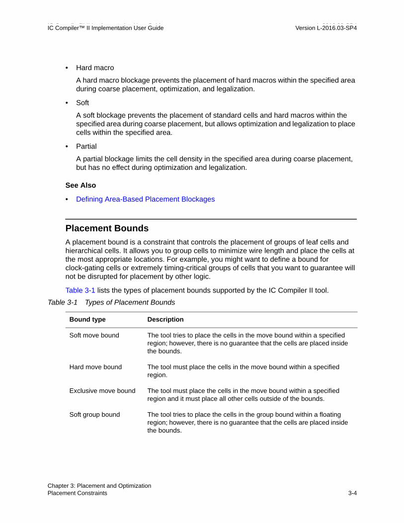
IC Compiler™ II Implementation User Guide L-2016.03-SP4IC Compiler™ II Implementation User Guide Version L-2016.03-SP4
• Hard macro
A hard macro blockage prevents the placement of hard macros within the specified area during coarse placement, optimization, and legalization.
• Soft
A soft blockage prevents the placement of standard cells and hard macros within the specified area during coarse placement, but allows optimization and legalization to place cells within the specified area.
• Partial
A partial blockage limits the cell density in the specified area during coarse placement, but has no effect during optimization and legalization.
See Also
• Defining Area-Based Placement Blockages
Placement Bounds
A placement bound is a constraint that controls the placement of groups of leaf cells and hierarchical cells. It allows you to group cells to minimize wire length and place the cells at the most appropriate locations. For example, you might want to define a bound for clock-gating cells or extremely timing-critical groups of cells that you want to guarantee will not be disrupted for placement by other logic.
Table 3-1 lists the types of placement bounds supported by the IC Compiler II tool.
Table 3-1 Types of Placement Bounds
Bound type Description
Soft move bound The tool tries to place the cells in the move bound within a specified region; however, there is no guarantee that the cells are placed inside the bounds.
Hard move bound The tool must place the cells in the move bound within a specified region.
Exclusive move bound The tool must place the cells in the move bound within a specified region and it must place all other cells outside of the bounds.
Soft group bound The tool tries to place the cells in the group bound within a floating region; however, there is no guarantee that the cells are placed inside the bounds.
Chapter 3: Placement and OptimizationPlacement Constraints 3-4

IC Compiler™ II Implementation User Guide Version L-2016.03-SP4
See Also
• Defining Placement Bounds
Voltage Areas
A voltage area is a physical placement area for the cells associated with a power domain. For multivoltage designs, the power domains are defined in the UPF specification. For single-voltage designs, the tool creates a default power domain when you read the Verilog netlist and associates it with a default voltage area, which comprises of the core area of the block.
The placer treats a voltage area the same as an exclusive move bound; it must place the cells in a voltage area within a specified region and it must place all other cells outside of the voltage area. Voltage areas can be rectangular or rectilinear. In addition, they can be disjoint, nested, or overlapping. For overlapping voltage areas, the effective shape of each voltage area is determined by the stacking order of the voltage area shapes.
See Also
• Defining Voltage Areas
• Loading the Power Intent
Hard group bound The tool must place the cells in the group bound within a floating region, whose actual coordinates are determined by the tool.
Dimensionless group bound
The tool determines the shape and location of the group bound based on the effort used to bring cells closer inside the group bound.
Table 3-1 Types of Placement Bounds (Continued)
Bound type Description
Chapter 3: Placement and OptimizationPlacement Constraints 3-5Chapter 3: Placement and OptimizationPlacement Constraints 3-5

IC Compiler™ II Implementation User Guide L-2016.03-SP4IC Compiler™ II Implementation User Guide Version L-2016.03-SP4
Density Constraints
Density constraints control how densely cells can be packed. You can control the overall placement density for the block or the cell density for specific regions. To control the cell density for specific regions, you use partial blockages.
See Also
• Controlling the Placement Density
• Defining a Partial Placement Blockage
Cell Spacing Constraints
Cell spacing constraints control the spacing between a standard cell and another standard cell or a boundary (the chip boundary, a hard macro, a hard macro keepout margin, a hard placement blockage, or a voltage area guard band). You assign library cells to groups (the boundaries are in a predefined group named SNPS_BOUNDARY), and then define the required spacing between cells in these groups.
See Also
• Defining Cell Spacing Constraints
Preparing for Placement and Optimization
Before you perform placement and optimization,
• Define the placement constraints, as described in the following topics:
❍ Defining Keepout Margins
❍ Defining Area-Based Placement Blockages
❍ Defining Placement Bounds
❍ Defining Voltage Areas
❍ Controlling the Placement Density
❍ Defining Cell Spacing Constraints
• Define a name prefix for the cells added during optimization, as described in Inserting Multivoltage Cells.
Chapter 3: Placement and OptimizationPreparing for Placement and Optimization 3-6

IC Compiler™ II Implementation User Guide Version L-2016.03-SP4
• Insert the multivoltage cells, as described in Inserting Multivoltage Cells.
• Mark the clock networks as ideal clocks, as described in Marking the Clock Networks.
See Also
• Preparing for Timing Analysis
• Preparing for Optimization
Defining Keepout Margins
The width of the keepout margin on each side of the fixed cell can be the same or different, depending on how you define the keepout margin. In addition, keepout margins can be defined as hard or soft.
To define a keepout margin, use the create_keepout_margin command. By default, the command creates a hard keepout margin. To create a soft keepout margin, use the -type soft option.
Defining an Outer Keepout Margin
You can define an outer keepout margin on a hard macro, a hierarchical cell, or a leaf cell. When you define an outer keepout margin, you can either specify the keepout distance explicitly or, for hard macros, you can have the tool derive the keepout distance based on the macro pin count.
To explicitly specify an outer keepout margin, use the -outer option to specify the margin distance for each side. You specify the left, bottom, right, and top margins using the following format: {lx by rx ty}. A value of 0 results in no keepout margin for that side.
For example, to create a hard outer keepout margin with a margin of 10 on each side for a macro named my_macro, use the following command:
icc2_shell> create_keepout_margin -outer {10 10 10 10} my_macro
To have the tool derive the outer keepout distance for a hard macro based on its pin count, use the -tracks_per_macro_pin option to specify the track-to-pin ratio. When you use this option, the tool calculates the keepout margin from the track width, the number of macro pins, and the specified track-to-pin ratio, which is typically set to a value near 0.5. A larger value results in larger keepout margins. The derived keepout margin is always hard; the -type setting is ignored. The derived margins are subject the minimum and maximum values specified by the -min_padding_per_macro and -max_padding_per_macro options.
Chapter 3: Placement and OptimizationPreparing for Placement and Optimization 3-7Chapter 3: Placement and OptimizationPreparing for Placement and Optimization 3-7

IC Compiler™ II Implementation User Guide L-2016.03-SP4IC Compiler™ II Implementation User Guide Version L-2016.03-SP4
For example, to have the tool derive the outer keepout margin for a macro named my_macro by using a track-to-pin ratio of 0.6 with a minimum keepout distance of 0.1 and a maximum keepout distance of 0.2, use the following command:
icc2_shell> create_keepout_margin -tracks_per_macro_pin 0.6 \-min_padding_per_macro 0.1 -max_padding_per_macro 0.2 my_macro
Defining an Inner Keepout Margin
You can define an inner keepout margin on a hierarchical cell, but not on a hard macro or a leaf cell. When you define an inner keepout margin, you must specify the keepout distance explicitly.
To explicitly specify an inner keepout margin, use the -inner option to specify the margin distance for each side. You specify the left, bottom, right, and top margins using the following format: {lx by rx ty}. A value of 0 results in no keepout margin for that side.
For example, to create a hard inner keepout margin with a margin of 10 on each side for a hierarchical cell named my_hcell, use the following command:
icc2_shell> create_keepout_margin -inner {10 10 10 10} my_hcell
Defining Area-Based Placement Blockages
To define placement blockages, use the create_placement_blockage command. At a minimum, you must specify the coordinates of the placement blockage. To create a rectangular placement blockage, use the -boundary option to specify the lower-left and upper-right coordinates of the rectangle. To create a rectilinear placement blockage, use the -boundary option to specify the coordinates of the polygon.
By default, the create_placement_blockage command creates a hard placement blockage. To create another type of placement blockage, use the -type option to specify the blockage type. A single create_placement_blockage command can create just one type of placement blockage.
You can optionally assign a name to a placement blockage by using the -name option. You can then reference that blockage by name to query or remove the placement blockage.
Defining a Hard Placement Blockage
To define a hard placement blockage, specify the boundary and optionally a name for the placement blockage.
For example, to create a hard placement blockage in the area enclosed by a rectangle with corners at (10, 20) and (100, 200), use the following command:
icc2_shell> create_placement_blockage -boundary {10 20 100 200}
Chapter 3: Placement and OptimizationPreparing for Placement and Optimization 3-8

IC Compiler™ II Implementation User Guide Version L-2016.03-SP4
Hard placement blockages can also be defined in the DEF as shown in Example 3-1.
Example 3-1 Placement Blockages in DEF
BLOCKAGES 2 ; - PLACEMENT RECT ( 0 327600 ) ( 652740 327660 ) ; - PLACEMENT RECT ( 0 327600 ) ( 652740 327660 ) ;END BLOCKAGES1
Defining a Hard Macro Placement Blockage
To define a hard macro blockage, specify the boundary, type (-type hard_macro option), and optionally the name for the placement blockage.
For example, to define a hard macro blockage enclosed by a rectangle with corners at (120, 75) and (230, 200), use the following command:
icc2_shell> create_placement_blockage -boundary {120 75 230 200} \-type hard_macro
Defining a Soft Placement Blockage
To define a soft blockage, specify the boundary, type (-type soft option), and optionally the name for the placement blockage.
For example, to define a soft blockage enclosed by a rectangle with corners at (120, 75) and (230, 200), use the following command:
icc2_shell> create_placement_blockage -boundary {120 75 230 200} \-type soft
A soft blockage prevents the coarse placement from placing cells within the specified area, but allows optimization and legalization to do so. However, after placement and optimization, during subsequent incremental placement, the tool can move the cells added during initial optimization out of the soft blockage area. To prevent this, use the following application option setting:
icc2_shell> set_app_options \-name place.coarse.enable_enhanced_soft_blockages -value true
Chapter 3: Placement and OptimizationPreparing for Placement and Optimization 3-9Chapter 3: Placement and OptimizationPreparing for Placement and Optimization 3-9

IC Compiler™ II Implementation User Guide L-2016.03-SP4IC Compiler™ II Implementation User Guide Version L-2016.03-SP4
Defining a Partial Placement Blockage
To define a partial blockage, specify the boundary, type (-type partial option), blockage percentage (-blocked_percentage option), and optionally the name for the placement blockage.
For example, to define a partial blockage with a maximum allowed cell density of 60 percent (a blocked percentage of 40), enclosed by the rectangle with corners at (10, 20) and (100, 200), use the following command:
icc2_shell> create_placement_blockage -boundary {10 20 100 200} \-type partial -blocked_percentage 40
Note: To allow unlimited usage of a partial blockage area, specify a blockage percentage of zero (–blocked_percentage 0 option).
Querying Placement Blockages
To return a collection of placement blockages in the current block that match certain criteria, use the get_placement_blockages command.
Removing Placement Blockages
To remove placement blockages from a block, use the remove_placement_blockages command. To remove all placement blockages from a block, use the -all option. To remove specific placement blockages from a block, specify the placement blockage names.
Defining Placement Bounds
To define a placement bound, use the create_bound command. When you define a bound, you must use the -name option to specify its name.
In general, you also specify the cells and ports to be included in the bound. If a hierarchical cell is included, all cells in the subdesign belong to the bound. However, you can create an empty bound and specify the contents of the bound later by using the add_to_bound command. You can remove objects from a bound by using the remove_from_bound command.
You must also specify the options required for the specific type of bound you want to create. The following topics describe how to create the various types of move bounds:
• Defining Move Bounds
• Defining Group Bounds
Chapter 3: Placement and OptimizationPreparing for Placement and Optimization 3-10

IC Compiler™ II Implementation User Guide Version L-2016.03-SP4
See Also
• Placement Bounds
Defining Move Bounds
A move bound is a fixed region within which to place a set of cells. It comprises of one or more rectangular or rectilinear shapes, which can be abutted, disjoint, or overlapping. To define the boundaries of these shapes, use the -boundary option with the create_bound command (if you are creating a new move bound) or the create_bound_shape command (if you are adding shapes to an existing move bound). Note that you can specify one or more shapes when using the create_bound command, but only a single shape in each create_bound_shape command.
• To specify the boundary of a rectangle shape, use the following format to specify its lower-left and upper-right corners:
{{llx lly} {urx ury}}
• To specify the boundary of a rectilinear shape, use the following format to specify the coordinates of its vertices:
{{x1 y1} {x2 y2} {x3 y3} {x4 y4} ...}
Move bounds can be hard, soft, or exclusive.
• To define a soft move bound, use the following syntax:
create_bound -name name [-type soft] -boundary {coordinates}[bound_objects]
For example, to define a rectangular soft move bound for the INST_1 cell instance with its lower-left corner at (100, 100) and its upper-right corner at (200, 200), use the following command:
icc2_shell> create_bound -name b1 -boundary {100 100 200 200} INST_1
• To define a hard move bound, use the following syntax:
create_bound -name name -type hard -boundary {coordinates}[bound_objects]
For example, to define a rectangular hard move bound for the INST_1 cell instance with its lower-left corner at (100, 100) and its upper-right corner at (200, 200), use the following command:
icc2_shell> create_bound -name b2 -type hard \-boundary {100 100 200 200} INST_1
Chapter 3: Placement and OptimizationPreparing for Placement and Optimization 3-11Chapter 3: Placement and OptimizationPreparing for Placement and Optimization 3-11

IC Compiler™ II Implementation User Guide L-2016.03-SP4IC Compiler™ II Implementation User Guide Version L-2016.03-SP4
• To define an exclusive move bound, use the following syntax:
create_bound -name name -exclusive -boundary {coordinates}[bound_objects]
For example, to define a rectangular exclusive move bound for the INST_1 cell instance with its lower-left corner at (100, 100) and its upper-right corner at (200, 200), use the following command:
icc2_shell> create_bound -name b3 -exclusive \-boundary {100 100 200 200} INST_1
To add shapes to an existing move bound, use the create_bound_shape command. To remove shapes from an existing move bound, use the remove_bound_shapes command.
Defining Group Bounds
A group bound is a floating region within which to place a set of cells. Group bounds can be hard, soft, or dimensionless.
• To define a soft group bound, use the following syntax:
create_bound -name name [-type soft] -dimensions {width height}[bound_objects]
For example, to define a soft group bound for the INST_1 and INST_2 cell instances with a width of 100 and a height of 100, use the following command:
icc2_shell> create_bound -name b4 -dimensions {100 100} \ {INST_1 INST_2}
• To define a hard group bound, use the following syntax:
create_bound -name name -type hard -dimensions {width height}[bound_objects]
For example, to define a hard group bound for the INST_1 and INST_2 cell instances with a width of 100 and a height of 100, use the following command:
icc2_shell> create_bound -name b5 -type hard -dimensions {100 100} \{INST_1 INST_2}
• To define a dimensionless group bound, use the following syntax:
create_bound -name name [-effort effort_level][bound_objects]
The default effort is medium; you can also specify low, high, or ultra.
Chapter 3: Placement and OptimizationPreparing for Placement and Optimization 3-12
IC Compiler™ II Implementation User Guide Version L-2016.03-SP4
For example, to define a dimensionless group bound for the INST_1 and INST_2 cell instances in which the tool uses a high level of effort to place the cells closer within the group bound, use the following command:
icc2_shell> create_bound -name b6 -effort high {INST_1 INST_2}
Querying Placement Bounds
To report the placement bounds in a block, use the report_bounds command.
To return a collection of placement bounds in the current block that match certain criteria, use the get_bounds command.
To return a collection of bound shapes associated with one or more move bounds, use the get_bound_shapes command.
Removing Placement Bounds
To remove placement bounds from a block, use the remove_placement_blockages command. To remove all placement bounds from a block, use the -all option. To remove specific placement bounds from a block, specify the placement bound names.
Generating Automatic Group Bounds for Clock Gating Cells
The tool can automatically generate group bounds for integrated clock gating cells and the sequential cells they drive. To do so, use the following application option setting:
icc2_shell> set_app_options -name place.coarse.icg_auto_bound -value true
When you enable this feature, the tool creates the automatic group bounds at the beginning of placement and removes them at the end of placement. The tool does not include cells that already belong to another group bound in the automatic group bounds.
To limit the maximum number of fanouts that can be included in an automatic bound, use the icg_auto_bound_fanout_limit application option setting, as shown in the following example:
icc2_shell> set_app_options \ -name place.coarse.icg_auto_bound_fanout_limit -value 30
The default fanout limit is 40.
Chapter 3: Placement and OptimizationPreparing for Placement and Optimization 3-13Chapter 3: Placement and OptimizationPreparing for Placement and Optimization 3-13

IC Compiler™ II Implementation User Guide L-2016.03-SP4IC Compiler™ II Implementation User Guide Version L-2016.03-SP4
Defining Voltage Areas
To define a voltage area, use the create_voltage_area command. When you define a voltage area, at a minimum, you must specify the power domains associated with the voltage area. To specify the power domains, use the -power_domains option. You can specify one or more power domains; however, all specified power domains must have the same primary supply net. If you specify a single power domain, the name of the voltage area is derived from the name of the power domain. If you specify multiple power domains, you must specify a name for the voltage area by using the -name option.
A voltage area consists of one or more rectangular or rectilinear shapes, which can be abutted, disjoint, or overlapping. To define the boundaries of these shapes, use the -region option with the create_voltage_area command (if you are creating a new voltage area) or the create_voltage_area_shape command (if you are adding shapes to an existing voltage area). Note that you can specify one or more shapes when using the create_voltage_area command, but only a single shape in each create_voltage_area_shape command.
• To specify the boundary of a rectangle shape, use the following format to specify its lower-left and upper-right corners:
{{llx lly} {urx ury}}
• To specify the boundary of a rectilinear shape, use the following format to specify the coordinates of its vertices:
{{x1 y1} {x2 y2} {x3 y3} {x4 y4} ...}
If a voltage area consists of multiple abutting or overlapping shapes, you can merge the shapes into a minimum set of disjoint shapes based on the stacking order of the shapes. For information about how to merge the voltage area shapes, see Merging Voltage Area Shapes.
The tool also uses the stacking order to resolve overlapping shapes from different voltage areas. For information about resolving overlapping voltage areas, see Resolving Overlapping Voltage Areas.
To ensure that no shorts occur at the boundaries of the voltage areas, you can define guard bands for the voltage areas, which act as hard keepout margins surrounding the voltage areas. If you define guard bands for a voltage area shape, the guard bands are included in the effective boundary of the shape; however, they are not included in the effective placement area of the voltage area. For information about defining guard bands, see Defining Guard Bands.
To modify an existing voltage area, use the set_voltage_area command, as described in Modifying Voltage Areas.
Chapter 3: Placement and OptimizationPreparing for Placement and Optimization 3-14

IC Compiler™ II Implementation User Guide Version L-2016.03-SP4
Multivoltage designs typically have power domains that are shut down and powered up during the operation of the chip while other power domains remain powered up. When dealing with shutdown domains, there can be some situations in which certain cells in the shutdown portion need to continuously stay active, such as for implementing retention registers, isolation cells, retention control paths, and isolation enable paths. These cells are referred to as always-on cells. To define a special placement area for always-on cells (an always-on well) within a voltage area, define an exclusive move bound within the boundary of the voltage area. For information about defining exclusive move bounds, see Defining Move Bounds.
After creating the voltage areas, run the check_mv_design command to verify that the design does not have any multivoltage violations.
Merging Voltage Area Shapes
To merge the voltage area shapes into a minimum set of disjoint shapes, use the -merge_regions option with the create_voltage_area, create_voltage_area_shape, or set_voltage_area command.
• When you use this option with the create_voltage_area command, it merges the shapes specified in the -region option.
• When you use this option with the create_voltage_area_shape command, it merges the shape specified in the -region option with the existing shapes of the specified voltage area.
• When you use this option with the set_voltage_area command, it merges all existing shapes of the specified voltage area.
The tool merges the voltage area shapes based on their stacking order. By default, the stacking order is the order in which you define the shapes, with the last shape defined on top. The merged shape replaces the top shape of a set of abutting or overlapping shapes; the other shapes in the set are removed and are no longer associated with the voltage area.
For example, assume that you use the following command to create a voltage area comprised of three rectangle shapes, as shown on the left side of Figure 3-2.
icc2_shell> create_voltage_area -power_domains {PD1} \ -region { {{0 0} {10 10}} {{10 0} {30 10}} {{15 5} {35 15}} }{PD1}icc2_shell> get_voltage_area_shapes -of_objects PD1 {VOLTAGE_AREA_SHAPE_1 VOLTAGE_AREA_SHAPE_2 VOLTAGE_AREA_SHAPE_3}
After you use the -merge_regions option to merge these shapes, the voltage area consists of a single rectilinear shape, as shown on the right side of Figure 3-2. The merged voltage
Chapter 3: Placement and OptimizationPreparing for Placement and Optimization 3-15Chapter 3: Placement and OptimizationPreparing for Placement and Optimization 3-15

IC Compiler™ II Implementation User Guide L-2016.03-SP4IC Compiler™ II Implementation User Guide Version L-2016.03-SP4
area shape is named VOLTAGE_AREA_SHAPE_3, which was the last voltage area shape defined when the voltage area was created.
icc2_shell> set_voltage_area PD1 -merge_regionsInformation: Merging abutted and overlapping shapes in voltage_area 'PD1'. (NDMUI-154)1icc2_shell> get_voltage_area_shapes -of_objects PD1{VOLTAGE_AREA_SHAPE_3}
Figure 3-2 Merging Voltage Area Shapes
To report the stacking order of the voltage area shapes, use the report_voltage_areas -verbose command.
To modify the stacking order of the voltage area shapes, use the set_voltage_area_shape command, as described in Modifying the Stacking Order.
Resolving Overlapping Voltage Areas
If voltage area shapes from two or more voltage areas overlap, either completely or partially, the tool uses the stacking order of the shapes to determine the effective shapes of the voltage areas. By default, the stacking order is the order in which you define the shapes, with the last shape defined on top. The tool assigns the overlapped region to the voltage area associated with the top shape. Unlike merging shapes within a voltage area, when the tool resolves overlapping shapes from different voltage areas, it does not remove any shapes; only the interpretation of the shapes changes.
For example, assume you want to create nested voltage areas, as shown in Figure 3-3.
Figure 3-3 Nested Voltage Areas
Chapter 3: Placement and OptimizationPreparing for Placement and Optimization 3-16
IC Compiler™ II Implementation User Guide Version L-2016.03-SP4
To generate these effective voltage areas, you must specify the outer voltage area first, followed by the inner voltage area, so that the voltage area shape for the inner voltage area is on top:
icc2_shell> create_voltage_area -power_domains PD1 \-region { {0 0} {30 30} }
{PD1}icc2_shell> create_voltage_area -power_domains PD2 \
-region { {10 10} {20 20} }{PD2}icc2_shell> get_attribute -objects [get_voltage_areas PD2] \
-name effective_shapes{{10.0000 10.0000} {20.0000 20.0000}}icc2_shell> get_attribute -objects [get_voltage_areas PD1] \
-name effective_shapes{{0.0000 0.0000} {10.0000 0.0000} {10.0000 20.0000} {20.0000 20.0000} {20.0000 10.0000} {10.0000 10.0000} {10.0000 0.0000} {30.0000 0.0000} {30.0000 30.0000} {0.0000 30.0000}}
If you specify the inner voltage area first, the shape for the outer voltage area is on top and it masks the inner voltage area, so it is ignored by the tool, as shown in the following example:
icc2_shell> create_voltage_area -power_domains PD2 \-region { {10 10} {20 20} }
{PD2}icc2_shell> create_voltage_area -power_domains PD1 \
-region { {0 0} {30 30} }{PD1}icc2_shell> get_attribute -objects [get_voltage_areas PD2] \
-name effective_shapesicc2_shell> get_attribute -objects [get_voltage_areas PD1] \
-name effective_shapes{{0.0000 0.0000} {30.0000 30.0000}}
To report the stacking order of the voltage area shapes, use the report_voltage_areas -verbose command.
To modify the stacking order of the voltage area shapes, use the set_voltage_area_shape command, as described in Modifying the Stacking Order.
Modifying the Stacking Order
You can modify the stacking order of the voltage area shapes by using the set_voltage_area_shape command.
• To raise a voltage area shape one position, use the -raise option.
• To lower a voltage area shape one position, use the -lower option.
• To move a voltage area shape to the top, use the -top option.
Chapter 3: Placement and OptimizationPreparing for Placement and Optimization 3-17Chapter 3: Placement and OptimizationPreparing for Placement and Optimization 3-17

IC Compiler™ II Implementation User Guide L-2016.03-SP4IC Compiler™ II Implementation User Guide Version L-2016.03-SP4
• To move a voltage area shape to the bottom, use the -bottom option.
• To move a voltage area shape directly above another shape, use the -above option.
• To move a voltage area shape directly below another shape, use the -below option.
Defining Guard Bands
Guard bands define hard keepout margins surrounding the voltage areas in which no cells, including level shifters and isolation cells, can be placed. The guard bands guarantee that the cells in different voltage areas are separated so that power planning does not introduce shorts.
By default, voltage areas do not have guard bands. To define guard bands, use the -guard_band option with the create_voltage_area or create_voltage_area_shape command to specify the horizontal and vertical guard band width for each shape specified in the -region option. The horizontal guard band width applies to all vertical edges of the voltage area, while the vertical guard band width applies to all horizontal edges of the voltage area.
Note: If you also use the -merge_regions option, you must specify the guard band widths for each disjoint shape after merging. You would typically use this option only when all the shapes to be merged are abutted or overlapping and therefore merge into a single shape.
The effective boundary of a voltage area shape includes its guard band; however, the effective placeable area of the shape does not.
For example, Figure 3-4 shows the guard band around the PD1 voltage area that is defined by the following command:
icc2_shell> create_voltage_area -power_domains PD1 \-region {{0 0} {30 0} {30 10} {40 10} {40 30} {20 30} {20 25} {0 25}} \-guard_band { {3 1} }
Figure 3-4 Voltage Area Guard Band
To determine the effective guard bands for abutting or overlapping shapes associated with the same voltage area, the tool merges the shapes as described in Merging Voltage Area Shapes and then applies the guard bands defined for the top shape to the merged shape.
Chapter 3: Placement and OptimizationPreparing for Placement and Optimization 3-18

IC Compiler™ II Implementation User Guide Version L-2016.03-SP4
For example, assume that you use the following command to define guard bands for the voltage area shapes shown on the right side of Figure 3-2:
icc2_shell> create_voltage_area -power_domains {PD1} \ -region { {{0 0} {10 10}} {{10 0} {30 10}} {{15 5} {35 15}} } \
-guard_band { {1 1} {3 3} {3 1} }{PD1}
In this case, the effective guard band is the same as the guard band shown in Figure 3-4, which is the guard band defined for the merged shape.
To determine the effective placement areas and guard bands for overlapping shapes associated with different voltage areas, the tool uses the effective boundaries to resolve the shapes as described in Resolving Overlapping Voltage Areas. The top shape retains it placement area and guard band; the effective placement area and guard bands of lower shapes does not include the overlapping region. Note that if abutting shapes have guard bands, they are no longer abutting, but overlapping, due to the effective boundary that includes the guard bands.
For example, assume that you use the following commands to define guard bands for the voltage areas shown in Figure 3-3:
icc2_shell> create_voltage_area -power_domains PD1 \-region {{0 0} {30 30}} -guard_band { {2 2} }
{PD1}icc2_shell> create_voltage_area -power_domains PD2 \
-region {{10 10} {20 20}} -guard_band { {2 2} }{PD2}
In this case, the effective placement area of PD1 is reduced by the effective boundary of PD2, which includes its guard band, as shown in Figure 3-5.
Figure 3-5 Effective Boundaries of Overlapping Voltage Areas
Chapter 3: Placement and OptimizationPreparing for Placement and Optimization 3-19Chapter 3: Placement and OptimizationPreparing for Placement and Optimization 3-19

IC Compiler™ II Implementation User Guide L-2016.03-SP4IC Compiler™ II Implementation User Guide Version L-2016.03-SP4
Querying Voltage Areas
You can query the following information about voltage areas:
• The voltage areas in the current block
To create a collection of voltage areas in the current block, including the default voltage area, use the get_voltage_areas command.
• Detailed information about the voltage areas
To display detailed information about voltage areas, including the default voltage area, use the report_voltage_areas command.
To include information about the voltage area shapes that comprise each voltage area, use the -verbose option with the report_voltage_areas command.
• Effective placement area of a voltage area
To display the effective placement area of a voltage area, query the effective_shapes attribute of the voltage area.
• Effective guard bands of a voltage area
To display the effective guard bands of a voltage area, query the effective_guard_band_boundaries attribute of the voltage area. Note that you can also query this attribute for individual voltage area shapes.
Modifying Voltage Areas
After you have created voltage areas, you can make the following modifications to a voltage area:
• Change the power domains associated with the voltage area
To change the power domains associated with a voltage area, use the -add_power_domains and -remove_power_domains options with the set_voltage_area command.
• Change the voltage area name
To change the name of the voltage area, use the -name option with the set_voltage_area command.
• Change the voltage area region
To add shapes to a voltage area, use the create_voltage_area_shape command. To remove shapes from a voltage area, use the remove_voltage_area_shapes command.
Chapter 3: Placement and OptimizationPreparing for Placement and Optimization 3-20

IC Compiler™ II Implementation User Guide Version L-2016.03-SP4
Removing Voltage Areas
To remove voltage areas from a block, use the remove_voltage_areas command. To remove all voltage areas from a block, use the -all option. To remove specific voltage areas from a block, specify the voltage area names.
Controlling the Placement Density
To control how densely cells can be packed, use the place.coarse.max_density application option. You can set this application option to a value between one and the overall average utilization of the block. Choosing a value near one allows cells to clump together more densely. A value of one allows no gaps between cells. You should choose a high value for blocks with low utilization to improve timing and a low value for congested blocks to avoid cell clumping. By default, this application option is set to 0, which disables this feature.
For example, if the utilization of a block is 40 percent, you can choose a value between 0.4 and 1.
icc2_shell> set_app_options -name place.coarse.max_density -value 0.6
Defining Cell Spacing Constraints
By default, there are no spacing constraints between standard cells during placement. To enhance yield, you can define the valid spacing between standard cells or between a standard cell and a boundary, which includes the chip boundary, a hard macro, a hard macro keepout margin, a hard placement blockage, or a voltage area guard band.
Note: The support for spacing constraints between standard cells and power or ground nets depends on how the net is represented in the block. If the power or ground net is defined as a complete blockage, the legalizer and the check_legality command ignore spacing rule violations between standard cells and the power or ground net. If the power or ground net is defined as a partial blockage, the legalizer and the check_legality command check for spacing rule violations between standard cells and the power or ground net.
Cell spacing constraints are implemented by attaching labels, which are similar to attributes, to the left and right sides of library cells, assuming that the cell is in its north orientation, and specifying the invalid spacings between these labels.
Chapter 3: Placement and OptimizationPreparing for Placement and Optimization 3-21Chapter 3: Placement and OptimizationPreparing for Placement and Optimization 3-21

IC Compiler™ II Implementation User Guide L-2016.03-SP4IC Compiler™ II Implementation User Guide Version L-2016.03-SP4
To define cell spacing constraints,
1. Add labels to the library cells that have spacing constraints by using the set_placement_spacing_label command.
You must specify the following information for each label:
❍ The label name (the -name option)
❍ The library cells to which to apply the label (the -lib_cells option)
❍ The sides of the library cells to which to apply the label (the -side option, which can take a value of right, left, or both)
The label definitions are additive; you can specify the same label to be used on the right side of some cells and the left side of other cells. For example, to assign a label named X to the right side of the cellA library cell and the left side of the cellB and cellC library cells, use the following commands:
icc2_shell> set_placement_spacing_label -name X \-lib_cells {cellA} -side right
icc2_shell> set_placement_spacing_label -name X \-lib_cells {cellB cellC} -side left
You can assign multiple labels to a side of a library cell. For example, to assign labels named Y and Z to the right side of the cellB library cell, use the following commands:
icc2_shell> set_placement_spacing_label -name Y \-lib_cells {cellB} -side right
icc2_shell> set_placement_spacing_label -name Z \-lib_cells {cellB} -side right
2. Define the spacing requirements between the labels by using the set_placement_spacing_rule command.
You must specify the following information for each rule:
❍ The labels being constrained (the -labels option)
You must specify exactly two labels in each set_placement_spacing_rule command. You can specify any of the labels defined by the set_placement_spacing_label command or the predefined SNPS_BOUNDARY label, which includes the chip boundary, hard macro boundaries, a hard macro keepout margins, hard placement blockages, and voltage area guard bands. The two labels can be the same or different.
❍ The range of invalid spacings, in number of unit tiles
For example, to specify that there must be at least one unit tile between labels X and Y (they cannot abut), use the following command:
icc2_shell> set_placement_spacing_rule -labels {X Y} {0 0}
Chapter 3: Placement and OptimizationPreparing for Placement and Optimization 3-22

IC Compiler™ II Implementation User Guide Version L-2016.03-SP4
To specify that there must be at least one unit tile between X labels and any boundary, use the following command:
icc2_shell> set_placement_spacing_rule -labels {X SNPS_BOUNDARY} {0 0}
To specify that two X labels cannot have a spacing of two unit tiles, use the following command:
icc2_shell> set_placement_spacing_rule -labels {X X} {2 2}
To specify that labels X and Z must have a spacing of less than two unit tiles or more than four unit tiles, use the following command:
icc2_shell> set_placement_spacing_rule -labels {X Z} {2 4}
Important: The cell spacing constraints are not saved with the block; they apply only to the current session and must be redefined in each session.
Reporting Cell Spacing Constraints
To report the cell spacing rules, use the report_placement_spacing_rules command. This command reports the cell spacing labels defined in the current session, the library cells (and their sides) to which they apply, and the rules defined for them.
Removing Cell Spacing Constraints
To remove spacing rules, use the remove_placement_spacing_rules command. You must specify which rules to remove.
• To remove all spacing rules, use the -all option.
• To remove a specific label and all rules associated with that label, use the -label option to specify the label.
• To remove a rule between labels, use the -rule option to specify two labels associated with the rule.
Inserting Multivoltage Cells
A multivoltage design requires special multivoltage cells, such as level shifters and isolation cells, at the interface between power domains. Level shifters are required between power domains that operate at different voltage levels, while isolation cells are required between power domains that are in different states (powered-down versus always-on or powered-up). Typically, multivoltage cells are inserted during logic synthesis; however, you can also insert them with the IC Compiler II tool.
Chapter 3: Placement and OptimizationPreparing for Placement and Optimization 3-23Chapter 3: Placement and OptimizationPreparing for Placement and Optimization 3-23

IC Compiler™ II Implementation User Guide L-2016.03-SP4IC Compiler™ II Implementation User Guide Version L-2016.03-SP4
Inserting Level Shifters
Level-shifter cells function as the interface between power domains that operate at different voltage levels. These cells ensure that the output transition of a driver can cause the receiving cell to switch even though the receiver is operating at a different voltage level.
Note: If the block was synthesized using Design Compiler, automatic level-shifter insertion is done as part of the compile_ultra command.
To insert level shifters in the current block, use the create_mv_cells command. The tool inserts the level shifters using the cell mapping and strategy defined in the UPF specification. When the tool inserts a level shifter, it sets a size_only attribute on the level shifter and a dont_touch attribute on the port-to-level-shifter net.
For information about defining the level-shifter cell mapping and insertion strategy, see the Synopsys Multivoltage Flow User Guide.
Inserting Isolation Cells
Isolation cells are used to selectively shut off the input side of the voltage interface of a power domain; they do not shift the voltage.
Note: Isolation cells should be instantiated at the RTL level to prevent formal verification errors; however, you can also insert them using the IC Compiler II tool.
To insert isolation cells in the current block, use the create_mv_cells command. The tool inserts the isolation shifters using the cell mapping and strategy defined in the UPF specification. When the tool inserts an isolation cell, it sets a size_only attribute on the level shifter and a dont_touch attribute on the port-to-level-shifter net.
For information about defining the isolation cell mapping and insertion strategy, see the Synopsys Multivoltage Flow User Guide.
Associating Power Strategies With Existing Multivoltage Cells
The IC Compiler II tool automatically associates power strategies with existing multivoltage cells when you run the associate_mv_cells or commit_upf command. If this automatic association is not correct, you can manually modify the associations by using the set_power_strategy_attribute command. To determine the power strategies for a power domain, use the get_power_strategies command.
Chapter 3: Placement and OptimizationPreparing for Placement and Optimization 3-24

IC Compiler™ II Implementation User Guide Version L-2016.03-SP4
Analyzing Multivoltage Cells
After inserting or associating multivoltage cells, use the report_mv_path command to analyze the multivoltage cells in the design. This command provides detailed information about the level shifters and isolation cells in the design. If the tool failed to insert or associate multivoltage cells, the report_mv_path command reports the causes for these failures.
You should also run the check_mv_design command to verify that the design does not have any multivoltage design violations.
Marking the Clock Networks
If a block does not contain clock trees, you should perform placement and optimization using ideal clocks.
To mark all clock networks as ideal, use the following command:
foreach_in_collection mode [all_modes] { current_mode $mode set_ideal_network [all_fanout -flat -clock_tree]}
To model the clock tree effects for placement, you should also define the uncertainty, latency, and transition constraints for each clock by using the set_clock_uncertainty, set_clock_latency, and set_clock_transition commands.
Before performing clock tree synthesis, you must use the remove_ideal_network command to remove the ideal setting on the fanout of the clock trees.
Performing Placement and Optimization
After you have finished design planning and power planning, you can perform placement, optimization, and legalization on your design. The following topics describe how to perform and control placement, optimization, and legalization:
• Introduction to Power Optimization
• Performing Power Optimization
• Enabling Scan Chain Optimization
• Enabling the Automatic Use of Nondefault Routing Rules During Preroute Optimization
• Enabling Global-Route-Based RC Estimation During Preroute Optimization
• Defining a Cell Name Prefix for Optimization
• Performing Standalone Placement and Legalization
Chapter 3: Placement and OptimizationPerforming Placement and Optimization 3-25Chapter 3: Placement and OptimizationPerforming Placement and Optimization 3-25

IC Compiler™ II Implementation User Guide L-2016.03-SP4IC Compiler™ II Implementation User Guide Version L-2016.03-SP4
• Performing Placement, Optimization, and Legalization With a Single Command
• Using Physical Guidance From the Design Compiler Tool
• Performing Multibit Banking
• Performing Incremental Placement and Optimization
• Performing Magnet Placement
• Refining Placement
• Performing Placement and Optimization on Multivoltage Blocks
Introduction to Power Optimization
The IC Compiler II tool can optimize both dynamic and static (leakage) power.
• Dynamic power
This is the energy dissipated due to the voltage or logic transitions in the design objects, such as cells, pins, and nets. The dynamic power consumption is directly proportional to the number and frequency of transitions in the design.
• Static (leakage) power
This is the energy dissipated even when there are no transitions in the circuit. This is also known as leakage power and depends on the device characteristics. The main contributor to leakage power is the sub-threshold-voltage leakage in the device. At lower technology nodes, leakage power consumption contributes significantly to the total power consumption of the circuit.
See Also
• Performing Power Optimization
Performing Power Optimization
The following topics describe how to enable the different types of power optimization the tool performs:
• Performing Low-Power Placement
• Performing Conventional Leakage-Power Optimization
• Performing Dynamic-Power Optimization
• Performing Total-Power Optimization
Chapter 3: Placement and OptimizationPerforming Placement and Optimization 3-26

IC Compiler™ II Implementation User Guide Version L-2016.03-SP4
• Performing Percentage Low-Threshold-Voltage Optimization
Performing Low-Power Placement
To setup for low power placement, which reduces dynamic power, perform the following:
1. Annotate switching activity on the design, as described in Annotating the Switching Activity.
2. Ensure that at least one scenario is enabled for dynamic-power optimization by using the set_scenario_status -dynamic_power true command.
3. Enable low-power placement by setting the place.coarse.low_power_placement application option to true.
When you use this setting, the tool performs low-power placement during the create_placement, refine_placement, place_opt, refine_opt, and clock_opt commands.
Performing Conventional Leakage-Power Optimization
To setup for conventional leakage-power optimization during the preroute optimization stage, perform the following:
1. Ensure that at least one scenario is enabled for leakage-power optimization by using the set_scenario_status -leakage_power true command.
2. Enable conventional leakage-power optimization by setting the opt.power.mode application option to leakage.
3. (Optional) Change the effort level for power optimization by setting the opt.power.effort application option to medium or high. The default is low.
When you use these settings, the tool performs conventional leakage-power optimization during the place_opt, refine_opt, and clock_opt commands. However, it does not perform any dynamic-power optimization.
Performing Dynamic-Power Optimization
To setup for dynamic-power optimization during the preroute optimization stage, perform the following:
1. Annotate switching activity on the design, as described in Annotating the Switching Activity.
2. Ensure that at least one scenario is enabled for dynamic-power optimization by using the set_scenario_status -dynamic_power true command.
Chapter 3: Placement and OptimizationPerforming Placement and Optimization 3-27Chapter 3: Placement and OptimizationPerforming Placement and Optimization 3-27

IC Compiler™ II Implementation User Guide L-2016.03-SP4IC Compiler™ II Implementation User Guide Version L-2016.03-SP4
3. Enable dynamic-power optimization by setting the opt.power.mode application option to dynamic.
4. (Optional) Change the effort level for power optimization by setting the opt.power.effort application option to medium or high. The default is low.
When you use these settings, the tool performs dynamic-power optimization during the place_opt, refine_opt, and clock_opt commands. However, it does not perform any leakage-power optimization.
Performing Total-Power Optimization
Total power optimization considers the combined leakage- and dynamic-power cost during optimization. To setup for total-power optimization,
1. Setup for leakage-power optimization by performing the following steps:
a. Ensure that at least one scenario is enabled for leakage-power optimization by using the set_scenario_status -leakage_power true command.
2. Setup for dynamic-power optimization by performing the following steps:
a. Annotate switching activity on the design, as described in Annotating the Switching Activity.
b. Ensure that at least one scenario is enabled for dynamic-power optimization by using the set_scenario_status -dynamic_power true command.
3. Enable total-power optimization at the preroute stage by setting the opt.power.mode application option to total.
4. (Optional) Change the effort level for power optimization by setting the opt.power.effort application option to medium or high. The default is low.
When you use this setting, the tool performs total-power optimization during the place_opt, refine_opt, and clock_opt commands.
Performing Percentage Low-Threshold-Voltage OptimizationIn a library with multiple-threshold-voltage cells,
• The lower-threshold-voltage cells have a higher leakage current, but better performance.
• The higher-threshold-voltage cells have a lower leakage current, but worse performance.
Percentage low-threshold-voltage optimization tries to find a balance between the power and performance goals by restricting the use of low-threshold-voltage cells.
Chapter 3: Placement and OptimizationPerforming Placement and Optimization 3-28

IC Compiler™ II Implementation User Guide Version L-2016.03-SP4
To enable percentage low-threshold-voltage optimization during the preroute optimization stage,
1. Ensure that at least one scenario is enabled for leakage-power optimization by using the set_scenario_status -leakage_power true command.
2. Identify the multiple-threshold-voltage cells in your libraries by using the set_threshold_voltage_group_type command, as described in Identifying Multiple-Threshold-Voltage Cells.
3. Specify a limit for the number of low-threshold-voltage in the design by using the set_max_lvth_percentage command, as described in Constraining the Number of Low-Threshold-Voltage Cells
4. Enable percentage low-threshold-voltage optimization by setting:
❍ Theopt.power.leakage_type application option to percentage_lvt.
❍ Theopt.power.mode application option to leakage.
When you use these settings, the tool performs percentage low-threshold-voltage optimization during the place_opt, refine_opt, and clock_opt commands. It does not perform conventional leakage-power optimization.
Enabling Scan Chain Optimization
During logic synthesis, sequential elements are replaced with scan cells that can be configured as serial chain-of-state elements to aid in testability. By setting certain test signals, the scan cells can either capture values from the functional combinational logic or the test data. In most cases, the order of the scan cells can be changed without affecting the testability of the device.
If you annotate the scan chain information on the block by reading a SCANDEF file, the coarse placer automatically optimizes the scan chains. During initial placement, the coarse placer focuses on the QoR for the functional nets by ignoring the scan chains. After initial placement, the coarse placer further improves the QoR by repartitioning and reordering the scan chains based on the initial placement.
Repartitioning scan chains involves swapping components across scan chains so that each chain contains components that are near each other. Using the placement information to repartition and reorder the scan chains provides the following benefits:
• Reduces scan chain wire length
• Minimizes congestion and improves routability
Figure 3-6 shows the wiring diagram for a block that contains scan chains that were synthesized by Design Compiler. Because these scan chains are not optimally ordered with
Chapter 3: Placement and OptimizationPerforming Placement and Optimization 3-29Chapter 3: Placement and OptimizationPerforming Placement and Optimization 3-29

IC Compiler™ II Implementation User Guide L-2016.03-SP4IC Compiler™ II Implementation User Guide Version L-2016.03-SP4
respect to actual placement and clock trees, they can cause congestion and increased net delays.
Figure 3-6 Scan Chains Before Physically Aware Optimizations
After repartitioning, the scan chains should consist of scan cells that are physically near each other, as shown in Figure 3-7. This represents a block with many scan chains.
Figure 3-7 Repartitioned Scan Chains
Enabling the Automatic Use of Nondefault Routing Rules During Preroute Optimization
To improve timing QoR, the tool can automatically use nondefault routing rules on timing critical nets during preroute optimization. In addition, the tool can guide the router to honor these nondefault rule assignments as soft constraints.
To enable this capability during
• The place_opt command, set the place_opt.flow.optimize_ndr application option to true
icc2_shell> set_app_options -name place_opt.flow.optimize_ndr \ -value true
Chapter 3: Placement and OptimizationPerforming Placement and Optimization 3-30

IC Compiler™ II Implementation User Guide Version L-2016.03-SP4
• The clock_opt command, set the clock_opt.flow.optimize_ndr application option to true
icc2_shell> set_app_options -name clock_opt.flow.optimize_ndr \ -value true
• The refine_opt command, set the refine_opt.flow.optimize_ndr application option to true
icc2_shell> set_app_options -name refine_opt.flow.optimize_ndr \ -value true
Enabling Global-Route-Based RC Estimation During Preroute Optimization
To improve correlation with the postroute stage of the design flow, you can enable global route based RC estimation during the place_opt, clock_opt, and refine_opt commands. With this feature, the tool uses global routes for all nets and identifies the layers with the most appropriate per-unit resistance values. The nets are then constrained to minimum and maximum layers for preroute RC estimation.
To enable this feature, use the opt.common.use_route_aware_estimation application option. If you set it to
• auto, the feature is enabled only when there is a variation in the per-unit resistance value of the different routing layers
• true, the feature is enabled irrespective of the variation in the per-unit resistance value of the different routing layers
This application option is false by default and setting it to auto or true disables layer optimization, which works only on timing critical nets.
If you enable this feature, use the remove_route_aware_estimation command to remove all global route based estimation before you perform routing.
Chapter 3: Placement and OptimizationPerforming Placement and Optimization 3-31Chapter 3: Placement and OptimizationPerforming Placement and Optimization 3-31
IC Compiler™ II Implementation User Guide L-2016.03-SP4IC Compiler™ II Implementation User Guide Version L-2016.03-SP4
Defining a Cell Name Prefix for Optimization
You can specify a name prefix for the cells added on the data nets during optimization by using the opt.common.user_instance_name_prefix application option.
The following example specifies a name prefix of
• PO_ for the cells added on the data nets during the place_opt command
• CO_ for the cells added on the data nets during the clock_opt command
• RO_ for the cells added on the data nets during the route_opt command
icc2_shell> set_app_options \ -name opt.common.user_instance_name_prefix -value "PO_"icc2_shell> place_opticc2_shell> set_app_options \ -name opt.common.user_instance_name_prefix -value "CO_"icc2_shell> clock_opticc2_shell> set_app_options \ -name opt.common.user_instance_name_prefix -value "PO_"icc2_shell> route_opt
To specify a name prefix for the cells added on the clock network during clock tree synthesis, use the cts.common.user_instance_name_prefix application option, as described in Defining a Name Prefix for Clock Cells.
Performing Standalone Placement and Legalization
To perform coarse placement, including high-fanout synthesis, use the create_placement command. If a block contains scan chains that were annotated on the block by reading a SCANDEF file, the coarse placer also performs scan chain optimization.
You can control the trade off between runtime and QoR by setting the -effort option.
To enable
• Timing-driven placement, use the -timing_driven option
• Congestion-driven placement, use the -congestion option
To control the CPU effort used for congestion removal, use the -congestion_effort option
• Congestion driven restructuring, use the -congestion_driven_restructuring option
When you use this option, the tool performs several iterations of placement and restructuring of the logic to help reduce congestion.
Chapter 3: Placement and OptimizationPerforming Placement and Optimization 3-32

IC Compiler™ II Implementation User Guide Version L-2016.03-SP4
To control the congestion driven restructuring,
❍ Specify the number of iterations of placement and restructuring to perform by using the place.coarse.cong_restruct_iterations application option. By default, the tool performs three iterations.
❍ Specify the effort level by using the place.coarse.cong_restruct_effort application option. The possible values are low, medium, high, and ultra, and the default is medium.
❍ Enable ungrouping of logic by using the place.coarse.cong_restruct_ungroup application option. The default is false.
❍ Enable the removal of buffers by using the place.coarse.cong_restruct_remove_buffers application option. The default is false.
To perform legalization, use the legalize_placement command.
See Also
• Loading a SCANDEF File
• Enabling Scan Chain Optimization
Performing Placement, Optimization, and Legalization With a Single Command
To perform coarse placement, physical optimization, and legalization with a single command, use the place_opt command.
This command supports multithreading and uses the number of threads specified by the set_host_options -max_cores command.
The place_opt command consists of the following stages:
1. Initial placement (initial_place)
During this stage, the tool performs coarse placement, which considers only the datapath timing requirements. If a block contains scan chains that were annotated by reading a SCANDEF file, the tool also performs scan chain optimization.
2. Initial DRC violation fixing (initial_drc)
During this stage, the tool removes existing buffer trees and performs high-fanout synthesis and electrical DRC violation fixing.
Chapter 3: Placement and OptimizationPerforming Placement and Optimization 3-33Chapter 3: Placement and OptimizationPerforming Placement and Optimization 3-33

IC Compiler™ II Implementation User Guide L-2016.03-SP4IC Compiler™ II Implementation User Guide Version L-2016.03-SP4
3. Initial optimization (initial_opto)
During this stage, the tool performs timing, area, congestion, and leakage-power optimization.
4. Final placement (final_place)
During this stage, the tool performs incremental placement to improve timing and routability.
5. Final optimization (final_opto)
During this stage, the tool performs further optimization.
6. Legalization
During this stage, the tool legalizes the placement.
When you run the place_opt command, by default, the tool runs all six stages of placement and optimization.
To limit the place_opt command to run only one or more of the first five stages, initial_place, initial_drc, initial_opto, final_place, and final_opto, followed by legalization, use the -from option to specify the stage from which you want to begin and the -to option to specify the stage after which you want to end.
If you do not specify the -from option, the tool begins from the initial_place stage. Similarly, if you do not specify the -to option, the tool continues until the final_opto stage is completed and legalizes the placement.
For example, to skip initial placement, but run all the other stages of optimization and placement on a design that has already completed initial placement, use the following command:
icc2_shell> place_opt -from initial_drc
Considering the Impact on Clock Structures During Placement
To consider the impact on clock structures during placement, set the place_opt.flow.clock_aware_placement application option to true before you run the place_opt command.
Enabling this feature helps to
• Improve the timing at the enable pins of clock gating cells
• Improve clock structures and reduce the number of clock buffers inserted during clock tree synthesis
Chapter 3: Placement and OptimizationPerforming Placement and Optimization 3-34

IC Compiler™ II Implementation User Guide Version L-2016.03-SP4
Creating a Temporary Clock Tree for Placement and Optimization
By default, the place_opt command uses ideal clock information during placement and optimization. However, you can specify that the tool builds a temporary clock tree and use propagated clock during the place_opt command by setting the place_opt.flow.trial_clock_tree application option to true.
After placement and optimization, when you perform clock tree synthesis by using the clock_opt or synthesize_clock_trees command, the tool removes the temporary clock tree and builds the actual clock tree. To ensure that the temporary clock tree correlates to the actual clock tree, specify your clock tree synthesis settings before you run the place_opt command.
Optimizing Integrated Clock-Gating Logic
The place_opt command can optimize integrated clock-gating cells, if the enable pin of the clock gate is in a critical timing path. To enable this feature, set the place_opt.flow.optimize_icgs application option to true.
During the integrated clock-gating cell optimization, the tool
• Performs clock-aware placement, irrespective of the setting of the place_opt.flow.clock_aware_placement application option, and places critical clock-gating cells and their fanouts at more optimal locations
• Builds a temporary clock tree, irrespective of the setting of the place_opt.flow.trial_clock_tree application option, and uses the clock tree to identify timing-critical clock-gating cells
• Splits clock-gating cells if the enable pin of the clock gate is in a critical timing path
You can control the extent of splitting by specifying a critical range using the place_opt.flow.optimize_icgs_critical_range application option.
When optimizing clock-gating cells, the place_opt command can only split these cells, not merge them. You can merge clock gating cells before you run the place_opt command by using the merge_clock_gates command.
Chapter 3: Placement and OptimizationPerforming Placement and Optimization 3-35Chapter 3: Placement and OptimizationPerforming Placement and Optimization 3-35
IC Compiler™ II Implementation User Guide L-2016.03-SP4IC Compiler™ II Implementation User Guide Version L-2016.03-SP4
Enabling Global Route Based High-Fanout Synthesis
When the tool performs high-fanout synthesis and electrical DRC violation fixing, by default, it uses virtual routes.
To use global route during high-fanout synthesis and electrical DRC violation fixing, set the place_opt.initial_drc.global_route_based application option before you run the place_opt command:
icc2_shell> set_app_options \-name place_opt.initial_drc.global_route_based -value 1
To enable an integrated two-pass initial placement flow, which includes a trial high-fanout synthesis, set the following application options before you run the place_opt command:
icc2_shell> set_app_options \-name place_opt.initial_drc.global_route_based -value 1
icc2_shell> set_app_options \-name place_opt.initial_place.two_pass -value true
The integrated two-pass initial placement flow consist of wire-length-driven placement, trial high-fanout synthesis, and timing-driven placement. The tool discards the trial high-fanout synthesis results, but retains the timing-driven placement and proceeds to global route based high-fanout synthesis.
For designs with fragmented floorplans, enabling the integrated two-pass initial placement flow and global route based high-fanout synthesis can help improve timing and reduce congestion.
Changing the Congestion Effort
By default, the place_opt command performs congestion optimization to improve the routability of the design. You cannot disable congestion optimization. However, you can control the effort expended during this optimization by using the place_opt.congestion.effort application option setting.
For example, to reduce the effort expended during congestion optimization use the following setting:
icc2_shell> set_app_options -name place_opt.congestion.effort -value low
Chapter 3: Placement and OptimizationPerforming Placement and Optimization 3-36

IC Compiler™ II Implementation User Guide Version L-2016.03-SP4
Enabling Layer Optimization
During preroute optimization, layer optimization assigns minimum and maximum layer constraints for longer and more timing-critical nets. These layer constraints and retained in the designs and honored during routing and postroute optimization. This improve design timing without affecting the routability of the design.
To enable layer optimization during the final optimization stage, use the place_opt.flow.optimize_layers application option setting before you run the place_opt command:
icc2_shell> set_app_options \-name place_opt.flow.optimize_layers -value true
Enabling Path Optimization
Path optimization is an incremental optimization capability that focus on improving the QoR of timing paths. By default, path optimization is performed as part of the refine_opt command. However, you can also enable it during the place_opt command by using setting the place_opt.flow.do_path_opt application option to true.
icc2_shell> set_app_options -name place_opt.flow.do_path_opt -value true
See Also
• Configuring Multithreading
• Restricting Library Cell Usage
• Performing Placement and Optimization on Multivoltage Blocks
• Introduction to Power Optimization
• Loading a SCANDEF File
• Enabling Scan Chain Optimization
Using Physical Guidance From the Design Compiler Tool
When you use the place_opt command to perform placement and optimization, you can use the Synopsys physical guidance information from the Design Compiler Graphical tool as a starting point.
Using Design Compiler Graphical placement provides the following benefits:
• Reduces the runtime of the placement step
• Achieves better correlation between the Design Compiler Graphical and IC Compiler II tools
Chapter 3: Placement and OptimizationPerforming Placement and Optimization 3-37Chapter 3: Placement and OptimizationPerforming Placement and Optimization 3-37

IC Compiler™ II Implementation User Guide L-2016.03-SP4IC Compiler™ II Implementation User Guide Version L-2016.03-SP4
To transfer the design from the Design Compiler Graphical tool, use a gate-level netlist in the Verilog format, along with the constraint information.
To preserve consistency and improve correlation, you must
• Use the same logical constraints, including timing and UPF information, in both tools.
However, you must convert the Design Compiler scenario constraints into the mode, corner, and scenario format supported by the IC Compiler II tool.
• Use the Design Compiler Graphical placement in the IC Compiler tool and the same floorplan and physical constraints in both tools.
However, you can provide additional floorplan information that is not currently supported by the Design Compiler Graphical tool, but is needed in the IC Compiler II tool for physical implementation.
To transfer the physical information (placement, floorplan, and physical constraints) from the Design Compiler Graphical tool, perform the following tasks:
• Use the write_def command in the Design Compiler Graphical tool to generate a DEF file and read it into the IC Compiler II tool by using the read_def -add_def_only_objects {cells} -convert_sites command.
The DEF file generated from the Design Compiler Graphical tool contains the following physical information:
❍ Die area, site rows, and tracks
❍ Locations and shapes of ports
❍ Locations of macros, standard cells and physical only cells
❍ Route guides and prerouted nets
❍ Placement blockages
• Create a Tcl file containing physical constraints not captured in the DEF file and apply those constraints to the design in the IC Compiler II tool.
Physical constraints not captured in DEF include
❍ Voltage area definitions
❍ Layer constraints
❍ Special route guides with utilization
❍ Special blockages with blocked layers
Chapter 3: Placement and OptimizationPerforming Placement and Optimization 3-38

IC Compiler™ II Implementation User Guide Version L-2016.03-SP4
To use of Synopsys physical guidance information in the IC Compiler II tool, set the place_opt.flow.do_spg application option before you run the place_opt command:
icc2_shell> set_app_options -name place_opt.flow.do_spg -value true
The following example script shows how to use the Synopsys physical guidance with the place_opt command:
# Read in the netlistread_verilog design_spg.v
# Apply the timing constraintssource timing_const.tcl
# Apply the UPF constraintsload_upf design.upf
# Apply the DEF file generated from the Design Compiler Graphical toolread_def -add_def_only_objects {cells} -convert_sites design_dcg.def
# Apply the placement constraints not supported by DEFsource placement_const.tcl
# Enable the Synopsys placement guidance flowset_app_options -name place_opt.flow.do_spg -value true
# Perform placement and optimizationplace_opt
For more information, see the Synopsys physical guidance information in the Design Compiler User Guide.
Performing Multibit Banking
The IC Compiler II tool can merge single-bit registers or single-bit multivoltage cells such as isolation or level-shifter cells and replace them with equivalent multibit cells, if such multibit cells are available. For example, the tool can merge eight 1-bit registers to form one 8-bit register bank or two 4-bit register banks.
Figure 3-8 shows how multiple single-bit registers can be replaced with a multibit register.
Chapter 3: Placement and OptimizationPerforming Placement and Optimization 3-39Chapter 3: Placement and OptimizationPerforming Placement and Optimization 3-39

IC Compiler™ II Implementation User Guide L-2016.03-SP4IC Compiler™ II Implementation User Guide Version L-2016.03-SP4
Figure 3-8 Replacing Multiple Single-Bit Register Cells With a Multibit Register Cell
Replacing single-bit cells with multibit cells reduces
• Area due to shared transistors and optimized transistor-level layout
• The total clock tree net length
• The number of clock tree buffers and clock tree power
The multibit banking flow consists of the following steps:
1. Perform initial placement by using the create_placement command.
2. Identify the groups of cells that can be replaced by multibit cells by using the identify_multibit command, as described in Identifying Multibit Banks.
3. Optimize the design by using the place_opt –from initial_drc command.
4. (Optional) If multibit banking does not improve QoR, split specific multibit banks into individual registers or smaller multibit banks by using the split_multibit command, as described in Splitting Multibit Banks.
Identifying Multibit Banks
To identify groups of registers, isolation cells, or level-shifter cells that can be replaced by multibit cells, use the identify_multibit command.
When you use the identify_multibit command, you must specify:
• How to apply the multibit banking information by using one of the following methods:
❍ To have the tool apply the banking information to the design, use the -apply option.
Two 1-bit register cells
One 2-bit register cellReplace with
D Q
D Q
2 2D Q
SISE
SISE
SISE
Chapter 3: Placement and OptimizationPerforming Placement and Optimization 3-40

IC Compiler™ II Implementation User Guide Version L-2016.03-SP4
❍ To manually apply the banking information, generate an output file containing create_multibit commands by using the -output_file option.
You can view the output, edit it if necessary, and apply it to the design by using the source command.
• The type of cells you want to bank by using one of the following methods:
❍ To identify groups of registers that can be banked, use the -register option.
❍ To identify groups of isolation or level-shifter cells that can be banked, use the -mv_cell option.
When banking registers with the -register option, optionally, you can
• Control the mapping of single bits to multibit banks by specifying an input map file using the -input_map_file option. This file contains mapping information about which multibit register bank replaces which single-bit registers, as shown in the following example:
reg_group_1 {REGX1 REGX2 REGX4}2 {1 MREG2}4 {1 MREG4}6 {1 MREG2}{1 MREG4}
This map file contains a functional group named reg_group_1, which specifies how single-bit registers of reference cell types REGX1, REGX2, and REGX4 can be grouped to form multibit registers as follows:
❍ The first line specifies that two single-bit registers can be combined to form a register bank consisting of one MREG2 reference cell.
❍ The second line specifies that four single-bit registers can be combined to form a register bank consisting of one MREG4 reference cell.
❍ The third line specifies that six single-bit registers can be combined to form a register bank consisting of one MREG2 and one MREG4 reference cells.
• Exclude registers based on their slack by using one of the following methods:
❍ Specify a slack threshold for register to be considered for banking by using the -slack_threshold option.
Registers with a slack less than the specified threshold are ignored. By default, the tool consider all registers for banking.
Chapter 3: Placement and OptimizationPerforming Placement and Optimization 3-41Chapter 3: Placement and OptimizationPerforming Placement and Optimization 3-41

IC Compiler™ II Implementation User Guide L-2016.03-SP4IC Compiler™ II Implementation User Guide Version L-2016.03-SP4
❍ Specify a slack threshold file, which contains a different slack threshold for different timing-paths groups, by using the -slack_threshold_file option.
The following is an example of a slack threshold file, which specifies a threshold of 1 for the path group named G_CLK and a threshold of 2 for the path group named M_CLK:
G_CLK : 1M_CLK : 2
In addition, you can optionally specify the following:
• A list of instances to exclude by using the -exclude_instance option.
• A list of library cells for which to exclude all instances by using the -exclude_library_cells option.
Splitting Multibit Banks
To improve local congestion or path slack, you can split a multibit bank into smaller multibit banks or single-bit cells by using the split_multibit command.
To split
• Multibit cells on paths with slack less than a specific value, use the -slack_threshold option.
When you use the -slack_threshold option, you can limit the splitting to specific path groups by using the -path_groups option.
The following example splits the multibit cells on paths with a slack worse than -1:
icc2_shell> split_multibit -slack_threshold -1
• A specific cell, specify the cell instance name and the reference names of the smaller cells using the -lib_cells option.
The following example splits the multibit cell instance named reg_gr0, which is a four-bit register bank, into two two-bit multibit banks:
icc2_shell> split_multibit reg_gr0 -lib_cells {lib1/MREG2 lib1/MREG2}
The split_multibit command only splits multibit cells that were created by the create_multibit or identify_multibit command.
Chapter 3: Placement and OptimizationPerforming Placement and Optimization 3-42

IC Compiler™ II Implementation User Guide Version L-2016.03-SP4
Performing Incremental Placement and Optimization
After a block has been through an initial placement and optimization with the place_opt command, you can perform incremental placement and optimization by using the refine_opt command.
The refine_opt command consists of the following five stages:
1. Initial path optimization (initial_path_opt)
During this stage, the tool performs initial path optimization, during which it incrementally moves register along timing paths to improve timing while ensuring that no other paths are negatively affected.
2. Incremental placement (inc_place)
During this stage, the tool performs incremental placement to reduce congestion and improve routability.
3. Incremental optimization (inc_opt)
During this stage, the tool performs incremental timing, area, congestion, and leakage-power optimization.
4. Final placement (final_path_opt)
During this stage, the tool performs the final phase of path optimization to improve timing.
5. Legalization
During this stage, the tool legalizes the placement.
When you run the refine_opt command, by default, the tool runs all five stages of placement and optimization.
To limit the refine_opt command to run only one or more of the first four stages (initial_path_opt, inc_place, inc_opt, and final_path_opt) followed by legalization, use the -from option to specify the stage from which you want to begin and the -to option to specify the stage after which you want to end placement and optimization.
If you do not specify the -from option, the tool begins from the initial_path_opt stage. Similarly, if you do not specify the -to option, the tool continues until the final_path_opt stage is completed. After the tool runs the stages you specify, it legalizes the placement.
For example, to skip the final path optimization stage, but run all the other stages of optimization and placement on a design that has already completed initial placement, use the following command:
icc2_shell> refine_opt -to inc_opt
Chapter 3: Placement and OptimizationPerforming Placement and Optimization 3-43Chapter 3: Placement and OptimizationPerforming Placement and Optimization 3-43

IC Compiler™ II Implementation User Guide L-2016.03-SP4IC Compiler™ II Implementation User Guide Version L-2016.03-SP4
Optimizing Specific Endpoints
By default, the tool performs incremental placement and optimization on the entire design. To optimize only certain endpoints in the design, specify them by using the -end_points option.
Enabling Layer Optimization During Path Optimization
To enable layer optimization during path optimization, use the refine_opt.flow.optimize_layers application option setting before you run the refine_opt command:
icc2_shell> set_app_options \-name refine_opt.flow.optimize_layers -value true
When you enable this feature, the tool uses the fastest two layers for layer assignment.
Performing Magnet Placement
To improve congestion for a complex floorplan or to improve timing for the design, you can use magnet placement to specify a fixed object as a magnet and have the tool place all the standard cells connected to the magnet object close to it. You can specify fixed macro cells, pins of a fixed macro cells, or I/O ports as the magnet object.
For best results, perform magnet placement before standard cell placement.
To perform magnet placement, use the magnet_placement command with a specification of the magnets and options for any special functions you need to perform.
Table 3-2 shows the magnet_placement options.
Table 3-2 The magnet_placement Command Options
To do this Use this option
Specify the cells to pull toward the magnet object. -cells cell_list
Enable the movement of cells marked as fixed or legalize-only.
-move_fixed
-move_legalize_only
Mark the moved cells as fixed or legalize-only after magnet placement.
-mark_fixed
-mark_legalize_only
Specify the number of logic levels from the magnet that are considered for magnet placement.
-logical_levels number
Chapter 3: Placement and OptimizationPerforming Placement and Optimization 3-44

IC Compiler™ II Implementation User Guide Version L-2016.03-SP4
The following examples use the datapaths shown in Figure 3-9.
Figure 3-9 Example of Pulling Cells in a Contiguous Datapath
The following command pulls all cells, C1 through C8, toward the C0 magnet object:
icc2_shell> magnet_placement C0
Exclude buffers and inverters when determining the level of logic.
-exclude_buffers
Prevent the tracing of paths at inputs of sequential cells when finding the cells to pull.
-stop_by_sequential_cells
Prevent the tracing of paths at the outputs of sequential cells when finding the cells to pull.
-stop_on_sequential_cells
Prevent the tracing of paths beyond the specified pins, ports, or cells when finding the cells to pull.
-stop_points
Prevent placing cells on soft blockages. By default, the command only avoids hard blockages.
-avoid_soft_blockage
Specify how to place cells when the magnet objects are multiple ports or long ports
-multiple_long_port_mode auto|nearby
Report the cells that will be moved toward the magnet object, but not pull them
-only_report_magnet_cells
Create a collection of cells that are being pull toward the magnet object.
-get_collection
Table 3-2 The magnet_placement Command Options (Continued)
To do this Use this option
C0 C1 C2 C6 C7
C3 C4 C5
C8
Chapter 3: Placement and OptimizationPerforming Placement and Optimization 3-45Chapter 3: Placement and OptimizationPerforming Placement and Optimization 3-45

IC Compiler™ II Implementation User Guide L-2016.03-SP4IC Compiler™ II Implementation User Guide Version L-2016.03-SP4
The following command pulls the C6, C7, and C8 cells toward the C2 magnet object:
icc2_shell> magnet_placement C2 -cells {C6 C7 C8}
Although the C3, C4, and C5 cells form a contiguous datapath, they are isolated from the C0 cell, so the following command pulls no cells toward the C0 cell.
icc2_shell> magnet_placement C0 -cells {C3 C4 C5}
The following command pulls no cells toward the C0 magnet object because the C3, C6, and C8 cells do not form a contiguous datapath.
icc2_shell> magnet_placement C0 -cells {C3 C6 C8}
Refining Placement
To refine the placement and minimize congestion, use the refine_placement command. By default, this command performs incremental placement and legalization on the entire design.
• To refine the placement of a specific region, use the -coordinates option and specify the coordinates of the region.
• To change the effort used for placement, use the -effort option and specify either low, medium, or high. The default is medium.
• To change the effort used for minimizing congestion, use the -congestion_effort option and specify either low, medium, or high. The default is medium.
• To control the perturbation of the existing placement, use the -perturbation_level option and specify either min, medium, high, or max. The default is medium.
Performing Placement and Optimization on Multivoltage Blocks
Placement and optimization automatically consider multivoltage constraints, such as voltage areas.
During placement, the tool
• Places cells within their associated voltage area or voltage area shape
• Places level shifters and isolation cells close to the voltage area boundaries
Chapter 3: Placement and OptimizationPerforming Placement and Optimization 3-46
IC Compiler™ II Implementation User Guide Version L-2016.03-SP4
During optimization, when the tool inserts buffers, it
1. Considers the related supplies of the driver and loads of the net and does a dynamic analysis of the power states using one of the following:
❍ The UPF power state table you created using the create_pst command
❍ The UPF power state groups you created using add_power_state command
2. Chooses a buffering supply that does not introduce new MV violations, based on the power states and the available supplies in the voltage area being buffered.
Single-rail buffers are preferred to dual-rail buffers to save power and area, and improve routability.
To understand how or whether specific nets will be buffered, use the check_bufferability command, as described in Analyzing the Bufferability of Nets.
Analyzing the Placement and Optimization Results
The IC Compiler II tool provides both report-based and GUI-based placement analysis capabilities. To learn about these capabilities, see
• Analyzing the Bufferability of Nets
• Reporting Utilization
• Reporting the Placement QoR
• Querying and Changing the Placement Status
• Analyzing the Placement in the GUI
Analyzing the Bufferability of Nets
To analyze whether a net in the current block can be buffered or to report why the net cannot be buffered, use the check_bufferability command. This command checks if there are
• Supply nets available for buffering the net in the specified voltage area
• Suitable library cells available for buffering the net
• Settings on the net that prevent buffering, such as ideal-network or don’t-touch constraint settings
Chapter 3: Placement and OptimizationAnalyzing the Placement and Optimization Results 3-47Chapter 3: Placement and OptimizationAnalyzing the Placement and Optimization Results 3-47

IC Compiler™ II Implementation User Guide L-2016.03-SP4IC Compiler™ II Implementation User Guide Version L-2016.03-SP4
With this command, you must specify the following:
• The net to analyze by using one of the following methods:
❍ Specify the net name using the -net option.
❍ Specify the driver and loads by using the -driver and -loads options, and the logical hierarchy in which to perform the analysis by using the -hierarchy option.
• The voltage area in which to analyze the bufferability by using the -voltage_area option.
For example, to analyze if buffers can be added on the net named n34 in the PD1 power domain, use the following command:
icc2_shell> check_bufferability -net n34 -voltage_area PD1Information: Can insert dual rail buffers (8 lib_cells) and inverters (6 lib_cells) with supply nets (power: VDDSW, ground: VSS). (MV-454)
To analyze whether buffers can be added between the top_reg_1_/Q driver pin and its top_U1_9/B load pin in the top hierarchy in the PD_TOP voltage area, use the following command:
icc2_shell> check_bufferability -driver top_reg_1_/Q \ -loads top_U1_9/B -hierarchy / -voltage_area PD_TOPInformation: Cannot insert buffers or inverters, because required supply nets are not available. (MV-459)
For a more detailed information about the bufferability of a net, use the -verbose option.
Reporting Utilization
The utilization of a block is calculated by using the following formula, where demand is the total area occupied by objects and capacity is the total available area:
Utilization = Demand / Capacity
To report the utilization, use the following steps:
1. (Optional) Create a configuration for reporting the utilization by using the create_utilization_configuration command.
When you use this command, you must specify a name of the configuration. In addition, you can
❍ Specify how the capacity is calculated by using the -capacity option
The valid values are core_area, boundary, site_array, and site_row.
Chapter 3: Placement and OptimizationAnalyzing the Placement and Optimization Results 3-48

IC Compiler™ II Implementation User Guide Version L-2016.03-SP4
❍ Exclude objects from the calculation by using the -exclude option.
The valid values are hard_macros, macro_keepouts, soft_macros, io_cells, fixed_cells, physical_only_cells, hard_blockages, soft_blockages, pg_straps, spare_cells, flip_chip_bump_cells, and all.
❍ Specify where to store it, thereby controlling the scope of the configuration, by using the -scope option
The valid values are tech, lib, and block.
❍ Overwrite an existing configuration by using the -force option
The following example creates a utilization configuration for the current block named config1 that uses the core area for calculating the capacity and excludes hard and soft placement blockages:
icc2_shell> create_utilization_configuration -scope block config1 \ -capacity core_area -exclude {hard_blockages soft_blockages}
To remove a utilization configuration, use the remove_utilization_configurations command.
2. Report the utilization by using the report_utilization command.
To specify a utilization configuration and where it is stored, use the -config and -scope options. The valid values for the-scope option are tech, lib, and block. If you do not specify the -scope option with the -config option, the tool first searches the current block, then the design library, and finally the technology library for the specified configuration.
To report the utilization for specific objects, use the -of_objects option and specify one or more blocks, voltage areas, site arrays, or bounds. All objects must be of the same type.
Chapter 3: Placement and OptimizationAnalyzing the Placement and Optimization Results 3-49Chapter 3: Placement and OptimizationAnalyzing the Placement and Optimization Results 3-49
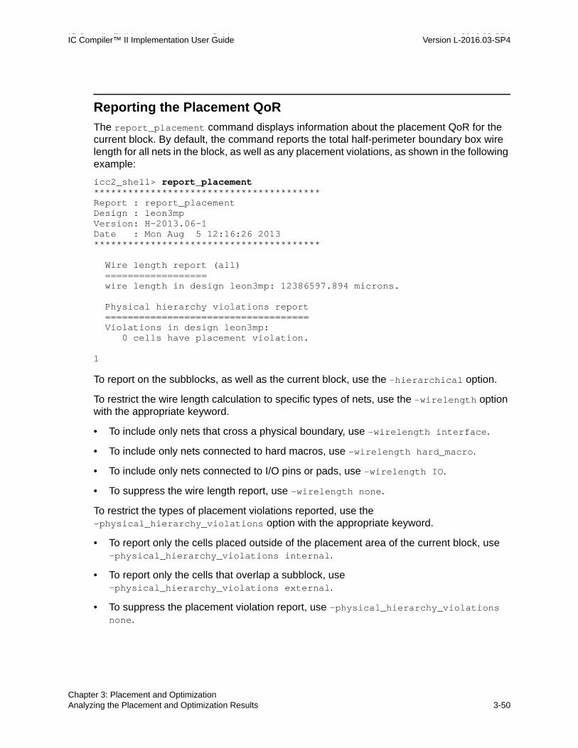
IC Compiler™ II Implementation User Guide L-2016.03-SP4IC Compiler™ II Implementation User Guide Version L-2016.03-SP4
Reporting the Placement QoR
The report_placement command displays information about the placement QoR for the current block. By default, the command reports the total half-perimeter boundary box wire length for all nets in the block, as well as any placement violations, as shown in the following example:
icc2_shell> report_placement****************************************Report : report_placementDesign : leon3mpVersion: H-2013.06-1Date : Mon Aug 5 12:16:26 2013****************************************
Wire length report (all)==================
wire length in design leon3mp: 12386597.894 microns.
Physical hierarchy violations report ==================================== Violations in design leon3mp:
0 cells have placement violation.
1
To report on the subblocks, as well as the current block, use the -hierarchical option.
To restrict the wire length calculation to specific types of nets, use the -wirelength option with the appropriate keyword.
• To include only nets that cross a physical boundary, use -wirelength interface.
• To include only nets connected to hard macros, use -wirelength hard_macro.
• To include only nets connected to I/O pins or pads, use -wirelength IO.
• To suppress the wire length report, use -wirelength none.
To restrict the types of placement violations reported, use the -physical_hierarchy_violations option with the appropriate keyword.
• To report only the cells placed outside of the placement area of the current block, use -physical_hierarchy_violations internal.
• To report only the cells that overlap a subblock, use -physical_hierarchy_violations external.
• To suppress the placement violation report, use -physical_hierarchy_violations none.
Chapter 3: Placement and OptimizationAnalyzing the Placement and Optimization Results 3-50

IC Compiler™ II Implementation User Guide Version L-2016.03-SP4
You can also report the following placement metrics:
• Swimming pool area
A swimming pool is a region that is enclosed by subblocks, hard macros, and placement blockages. Swimming pools can make it difficult to successfully place or route the block and should either be covered with a placement blockage or removed.
To report the total swimming pool area in the current block, use the -swimming_pool_area option.
• Thin channel area
A thin channel is a narrow region between subblocks of the current block, whether they are hard macros or physical hierarchies. Thin channels can make it difficult to successfully place or route the block and should either be covered with a placement blockage or widened.
To report the total thin channel area in the current block, use the -thin_channel_area option.
• Wire length of nets routed over hard macros
To report the wire length of nets routed over hard macros in the current block, use the -hard_macro_route_over option. This option reports the horizontal and vertical wire length for each hard macro that has over-macro routing, as well as the total wire length for over-macro routing.
• The number of hard macro overlaps
To report the total number of overlapping hard macros in the current block, use the -hard_macro_overlap option.
Chapter 3: Placement and OptimizationAnalyzing the Placement and Optimization Results 3-51Chapter 3: Placement and OptimizationAnalyzing the Placement and Optimization Results 3-51

IC Compiler™ II Implementation User Guide L-2016.03-SP4IC Compiler™ II Implementation User Guide Version L-2016.03-SP4
Querying and Changing the Placement Status
The status attribute of a cell instance indicates the current status of its placement. Table 3-3 shows the possible values of the status attribute.
To get the placement status of a cell instance, query its status attribute by using the get_attribute command. For example, to get the placement status of the cell instance named INST1, use the following command:
icc2_shell> get_attribute -objects [get_cells INST1] -name status
To change the placement status of a cell instance, use the set_placement_status command. For example, to set the placement status of the cell instance named INST1 to fixed, so that it is not moved during subsequent optimization and placement, use the following command:
icc2_shell> set_placement_status fixed [get_cells INST1]
Table 3-3 Placement Status Keywords
Placement status Description DEF syntax
unplaced The cell instance has not yet been placed.
Note: To revert all placed cells to the unplaced state, use the reset_placement command. This command modifies the placement status only for cells with a placement status of placed; it does not modify the placement status for cells with a placement status of fixed or locked.
+UNPLACED
placed The cell instance has been placed, but can be moved by subsequent operations.
+PLACED
fixed The cell instance has been placed and can be sized but not moved by subsequent operations.
Note: To prevent these cells from being sized, you must set a dont_touch attribute on these cells, as described in Preventing Optimization on Cells and Nets.
+FIXED
legalize_only The cell instance has been placed and can be moved only by the legalizer.
N/A
locked The cell instance has been placed and cannot be moved either manually or by the tool.
+COVER
Chapter 3: Placement and OptimizationAnalyzing the Placement and Optimization Results 3-52

IC Compiler™ II Implementation User Guide Version L-2016.03-SP4
Analyzing the Placement in the GUI
The IC Compiler II tool graphical user interface (GUI) provides the following tools for analyzing and visualizing the quality of results after placement:
• Cell Density Map
You can use the cell density map to identify areas of high cell density in the block or in a rectangular area of the block.
• Pin Density Map
You can use the pin density map to identify areas of high pin density in the block or in a rectangular area of the block.
• Global Route Congestion Map
You can use the global route congestion map to visualize the quality of placement with respect to the avoidance of routing congestion.
Cell Density Map
To display a cell density map for the current block,
1. Choose Placement > Cell Density Map.
The GUI displays the Map Mode panel, which offers you the option to specify the analysis grid dimensions, solid or unfilled grid units, the number of histogram bins, the bin threshold levels, and the utilization text display, as shown in the following figure.
Figure 3-10 Cell Density Map Mode Panel
Chapter 3: Placement and OptimizationAnalyzing the Placement and Optimization Results 3-53Chapter 3: Placement and OptimizationAnalyzing the Placement and Optimization Results 3-53
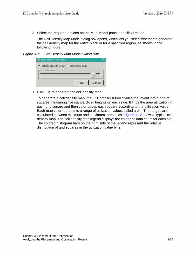
IC Compiler™ II Implementation User Guide L-2016.03-SP4IC Compiler™ II Implementation User Guide Version L-2016.03-SP4
2. Select the required options on the Map Model panel and click Reload.
The Cell Density Map Mode dialog box opens, which lets you select whether to generate the cell density map for the entire block or for a specified region, as shown in the following figure.
Figure 3-11 Cell Density Map Mode Dialog Box
3. Click OK to generate the cell density map.
To generate a cell density map, the IC Compiler II tool divides the layout into a grid of squares measuring five standard-cell heights on each side. It finds the area utilization in each grid square and then color-codes each square according to the utilization value. Each map color represents a range of utilization values called a bin. The ranges are calculated between minimum and maximum thresholds. Figure 3-12 shows a typical cell density map. The cell density map legend displays the color and data count for each bin. The colored histogram bars on the right side of the legend represent the relative distribution of grid squares in the utilization value bins.
Chapter 3: Placement and OptimizationAnalyzing the Placement and Optimization Results 3-54

IC Compiler™ II Implementation User Guide Version L-2016.03-SP4
Figure 3-12 Cell Density Map, Full-Chip View
Chapter 3: Placement and OptimizationAnalyzing the Placement and Optimization Results 3-55Chapter 3: Placement and OptimizationAnalyzing the Placement and Optimization Results 3-55

IC Compiler™ II Implementation User Guide L-2016.03-SP4IC Compiler™ II Implementation User Guide Version L-2016.03-SP4
When the view is zoomed in enough, the utilization values are displayed inside the grid squares, as shown in Figure 3-13. Otherwise, the text values are omitted from the display. Figure 3-13 shows both a solid-filled grid display and an unfilled grid display.
Figure 3-13 Cell Density Maps With and Without Solid Filled Grids
Cell Density Map Without Solid Filled Grids
Cell Density Map With Solid Filled Grids
Chapter 3: Placement and OptimizationAnalyzing the Placement and Optimization Results 3-56

IC Compiler™ II Implementation User Guide Version L-2016.03-SP4
To facilitate your analysis, you can change the Map Mode panel options to
• Display or hide individual map colors (bins)
• Adjust the map grid display
❍ Grid dimensions (height in number of standard cells)
❍ Grid size (as a function of grid dimensions and number of bins)
❍ Filled grids (solid or by fill pattern)
• Recalculate the cell density ranges
By default, when you change options on the Map Mode panel, the options turn blue; you must click Apply before the changes take effect in the layout view. You can enable a mechanism that automatically applies changes when you make them by choosing Options > Auto Apply.
Pin Density Map
To display a pin density map for the current block,
1. Choose Placement > Pin Density Map.
The GUI displays the Map Mode panel, which offers you the option to specify the analysis grid dimensions, solid or unfilled grid units, the number of histogram bins, the bin threshold levels, and the utilization text display, as shown in the following figure.
Figure 3-14 Pin Density Map Mode Panel
Chapter 3: Placement and OptimizationAnalyzing the Placement and Optimization Results 3-57Chapter 3: Placement and OptimizationAnalyzing the Placement and Optimization Results 3-57

IC Compiler™ II Implementation User Guide L-2016.03-SP4IC Compiler™ II Implementation User Guide Version L-2016.03-SP4
2. Select the required options on the Map Model panel and click Reload.
The Pin Density Map Mode dialog box opens, which lets you select whether to generate the pin density map for the entire block or for a specified region, as shown in the following figure.
Figure 3-15 Pin Density Map Mode Dialog Box
3. Click OK to generate the pin density map.
To generate a pin density map, the IC Compiler II tool divides the core area into a grid of squares measuring five standard-cell heights on each side. It finds the pin count in each grid square and then color-codes each square according to the pin density. Each map color represents a range of density values called a bin. The ranges are calculated between minimum and maximum thresholds. Figure 3-16 shows a typical pin density map. The pin density map legend displays the color and pin count range for each bin. The colored histogram bars on the right side of the legend represent the relative distribution of grid squares in the pin count value bins.
Chapter 3: Placement and OptimizationAnalyzing the Placement and Optimization Results 3-58

IC Compiler™ II Implementation User Guide Version L-2016.03-SP4
Figure 3-16 Pin Density Map, Full-Chip View
To facilitate your analysis, you can change the Map Mode panel options to
• Display or hide individual map colors (bins)
• Adjust the map grid display
❍ Grid dimensions (height in number of standard cells)
❍ Grid size (as a function of grid dimensions and number of bins)
❍ Filled grids (solid or by fill pattern)
• Recalculate the cell density ranges
By default, when you change options on the Map Mode panel, the options turn blue; you must click Apply before the changes take effect in the layout view. You can enable a mechanism that automatically applies changes when you make them by choosing Options > Auto Apply.
Chapter 3: Placement and OptimizationAnalyzing the Placement and Optimization Results 3-59Chapter 3: Placement and OptimizationAnalyzing the Placement and Optimization Results 3-59

IC Compiler™ II Implementation User Guide L-2016.03-SP4IC Compiler™ II Implementation User Guide Version L-2016.03-SP4
Global Route Congestion Map
To display a global route congestion map for the current block,
1. Choose Placement > Global Congestion Map.
The GUI displays the Map Mode panel, which offers you the option to specify the analysis grid dimensions, solid or unfilled grid units, the number of histogram bins, the bin threshold levels, and the utilization text display, as shown in the following figure.
Figure 3-17 Global Route Congestion Map Mode Panel
2. Select the required options on the Map Model panel and click Reload.
The (Re)Calculate Global Route Congestion Map Data dialog box opens, which lets you specify the command used to generate the congestion data, as shown in the following figure.
Figure 3-18 Global Route Congestion Map Mode Dialog Box
Chapter 3: Placement and OptimizationAnalyzing the Placement and Optimization Results 3-60

IC Compiler™ II Implementation User Guide Version L-2016.03-SP4
3. Click OK to generate the global route congestion map.
To generate a congestion map, the IC Compiler II tool divides the core area into a grid of colored boxes. Each box represents a vertical plane and a horizontal plane through which routes can pass. The left and bottom box edges are colored and labeled to show the usage-to-capacity ratios of the routes or routing tracks through the planes. Each map color represents a range of congestion values called a bin. The ranges are calculated by using a linear interpolation of the congestion data between minimum and maximum thresholds. The following figure shows a typical global route congestion map. The global route congestion map legend displays the color and data count for each bin. The colored histogram bars on the right side of the legend represent the relative distribution of congestion values in the bins.
Figure 3-19 Global Route Congestion Map
Chapter 3: Placement and OptimizationAnalyzing the Placement and Optimization Results 3-61Chapter 3: Placement and OptimizationAnalyzing the Placement and Optimization Results 3-61

IC Compiler™ II Implementation User Guide L-2016.03-SP4IC Compiler™ II Implementation User Guide Version L-2016.03-SP4
Analyzing the Timing
The IC Compiler II tool provides both report-based and GUI-based timing analysis capabilities. To learn about these capabilities, see
• Generating Timing Reports
• Analyzing Violations That Cannot Be Fixed
Generating Timing Reports
The IC Compiler II tool automatically updates timing and delay estimation results when needed. However, you can explicitly update the timing by using the update_timing command.
You can use the following commands to generate timing reports for a block:
• report_timing
The report_timing command reports the worst-case timing paths for the current block. For more information about this report, see Reporting the Worst-Case Timing Paths.
• report_qor
The report_qor command displays QoR information and statistics for the current block. For more information about this report, see Reporting the QoR.
• report_constraints
The report_constraints command reports the logical DRC violations for the current block. For more information about this report, see Reporting the Logical DRC Violations.
By default, these commands report the timing information using the current mode and corner. To report other modes, use the -modes option. To report other corners, use the -corners option.
Reporting the Worst-Case Timing Paths
To report the worst-case timing paths, use the report_timing command. By default, the command reports the path having the worst maximum (setup) delay across all active scenarios for the current mode that are enabled for setup analysis. Net delays are based on estimated route lengths.
To report the timing for all scenarios associated with specific modes, use the -modes option. To report the timing for all scenarios associated with specific corners, use the -corners
Chapter 3: Placement and OptimizationAnalyzing the Timing 3-62

IC Compiler™ II Implementation User Guide Version L-2016.03-SP4
option. To report the timing for specific scenarios, use the -scenarios option. Note that setup analysis must be enabled for the scenarios selected for reporting.
Example 3-2 shows the results of a typical report_timing command.
Example 3-2 report_timing Report Example
icc2_shell> report_timing****************************************Report : timing -path_type full -delay_type max -nworst 1 -max_paths 1
-report_by design-nets-physical-attributes
Design : my_designVersion: J-2014.06Date : Tue Aug 5 16:16:31 2014****************************************... Startpoint: u0_3/p0/mul0/m0_U1_INT_SUMR_reg_1_/CLK (rising edge-triggered flip-flop) Endpoint: u0_3/p0/iu0/r_reg_E__OP2__31_/D (rising edge-triggered flip-flop) Mode: my_mode Corner: wc_corner Scenario: wc_scenario Path Group: pci_clk Path Type: max Launch clock: pci_clk r Capture clock: pci_clk r
Attributes b - black-box (unknown) s - size_only d - dont_touch u - dont_use g - generic h - hierarchical i - ideal n - noncombinational E - extracted timing model Q - Quick timing model
Point Fanout Cap Trans Incr Path------------------------------------------------------------------------------------- clock pci_clk (rise edge) 0.00 0.00 clock network delay (ideal) 2.00 2.00 u0_3/p0/mul0/m0_U1_INT_SUMR_reg_1_/CLK (SDFFX1_LVT) 0.00 0.00 2.00 r u0_3/p0/mul0/m0_U1_INT_SUMR_reg_1_/QN (SDFFX1_LVT) 1 7.19 0.11 0.18 2.18 f... u0_3/p0/iu0/U6660/S (MUX21X1_LVT) 0.22 0.00 6.26 r u0_3/p0/iu0/U6660/Q (MUX21X1_LVT) 1 1.78 0.11 0.11 6.37 f u0_3/p0/iu0/r_reg_E__OP2__31_/D (SDFFX1_LVT) 0.11 0.00 6.37 f data arrival time 6.37
Chapter 3: Placement and OptimizationAnalyzing the Timing 3-63Chapter 3: Placement and OptimizationAnalyzing the Timing 3-63

IC Compiler™ II Implementation User Guide L-2016.03-SP4IC Compiler™ II Implementation User Guide Version L-2016.03-SP4
clock pci_clk (rise edge) 5.00 5.00 clock network delay (ideal) 2.00 7.00 clock uncertainty -0.40 6.60 library setup time -0.20 6.40 data required time 6.40------------------------------------------------------------------------------------- data required time 6.40 data arrival time -6.37------------------------------------------------------------------------------------- slack (MET) 0.03
The default report shows the startpoint, endpoint, path group (clock domain), path type (minimum delay, maximum delay, maximum rise, minimum fall, and so on), the incremental and cumulative time delay values along the data and clock paths, the data required time at the path endpoint, and the timing slack for the path. By default, the report_timing command considers an endpoint only one time across the specified scenarios (or default scenarios, if none are specified). You can choose to consider an endpoint one time per scenario, mode, corner, or path group by using the -report_by option.
The report_timing command options let you specify the scope of paths reported (from, to, or through specified points in the block), the path types reported, the numbers of worst-case paths reported, and the types of information reported for intermediate points in the path (transition times, capacitance, net delays, and so on).
To get a detailed report about the delay calculation at a given point along a timing path, use the report_delay_calculation command. Use the -from and -to options to specify the “from” and “to” pins of the cell or net that you want to report. These two pins can be the input and output pins of a cell to report the calculation of a cell delay, or can be the driver pin and a load pin of a net to report the calculation of a net delay. By default, the command reports the delay calculation for the current scenario. You can specify the mode and corner to report with the -mode and -corner option, respectively, or you can specify the scenario to report by using the -scenario option.
Chapter 3: Placement and OptimizationAnalyzing the Timing 3-64

IC Compiler™ II Implementation User Guide Version L-2016.03-SP4
Example 3-3 shows a report generated by the report_delay_calculation command for the current scenario.
Example 3-3 Delay Calculation Report
icc2_shell> report_delay_calculation \-from u0_3/p0/mul0/m0_U1_INT_SUMR_reg_1_/CLK \-to u0_3/p0/mul0/m0_U1_INT_SUMR_reg_1_/QN
****************************************Report : delay_calculationModule : placedMode : my_modeCorner : wc_modeVersion: J-2014.06Date : Tue Aug 5 16:29:52 2014****************************************
cap units: 1.00fF res units: 1.00MOhm time units: 1.00ns
Current delay calculation style: autoCurrent min Elmore tau: 0.00sCurrent min Arnoldi tau: 2.00ps
Cell arc:Lib: /usr/libs/mylib.ndm:mylib_lvtCell: u0_3/p0/mul0/m0_U1_INT_SUMR_reg_1_ (FD1_LVT)From-pin: CLK To-pin: QN
Sense: rising_edge
Input Output Stored Stored Delay slew Load Delay slew delay output slew derateearly rise: 0.29 7.27 0.22 0.11 0.22 0.11 0.99 late rise: 0.29 7.27 0.22 0.11 0.22 0.11 1.01early fall: 0.29 6.85 0.20 0.10 0.20 0.10 0.99 late fall: 0.29 6.85 0.20 0.10 0.20 0.10 1.01
1
Reporting the QoR
The report_qor command displays information about the quality of results and other statistics for the current block. It reports information about timing path group details and cell count and current block statistics, including combinational, noncombinational, and total area. The command also reports static power and design rule violations.
By default, the command reports the QoR for all active scenarios. To report the QoR for all scenarios associated with specific modes, use the -modes option. To report the QoR for all
Chapter 3: Placement and OptimizationAnalyzing the Timing 3-65Chapter 3: Placement and OptimizationAnalyzing the Timing 3-65

IC Compiler™ II Implementation User Guide L-2016.03-SP4IC Compiler™ II Implementation User Guide Version L-2016.03-SP4
scenarios associated with specific corners, use the -corners option. To report the QoR for specific scenarios, use the -scenarios option.
Example 3-4 shows a report generated by the report_qor command. In the Cell Count section, the report shows the number of macros in the block. To qualify as a macro cell, a cell must not be hierarchical and must have the is_macro_cell attribute set on its library cell.
Example 3-4 report_qor Report Example
icc2_shell> report_qor****************************************Report : qorDesign : placedVersion: J-2014.06Date : Tue Aug 5 16:33:05 2014****************************************
Information: Design Average RC value per unit length: (NEX-011)Information: r = 1.792938 ohm/um, c = 0.079907 ff/um, cc = 0.000000 ff/um (X dir) (NEX-017)Information: r = 1.785714 ohm/um, c = 0.093680 ff/um, cc = 0.000000 ff/um (Y dir) (NEX-017)
Scenario 'bc_scenario'Timing Path Group 'pci_clk'----------------------------------------Worst Hold Violation: -0.15Total Hold Violation: -8.79No. of Hold Violations: 283----------------------------------------...
Scenario 'wc_scenario'Timing Path Group 'pci_clk'----------------------------------------Levels of Logic: 55Critical Path Length: 2.79Critical Path Slack: 0.03Critical Path Clk Period: 3.00Total Negative Slack: 0.00No. of Violating Paths: 0----------------------------------------...
Cell Count----------------------------------------Hierarchical Cell Count: 694Leaf Cell Count: 116919Buf/Inv Cell Count: 17031CT Buf/Inv Cell Count: 0----------------------------------------
Chapter 3: Placement and OptimizationAnalyzing the Timing 3-66

IC Compiler™ II Implementation User Guide Version L-2016.03-SP4
Area----------------------------------------Combinational Area: 8365846.92Noncombinational Area: 571218.74Net Area: 0Net XLength: 0Net YLength: 0----------------------------------------Cell Area: 8937065.66Design Area: 8937065.66Net Length: 0
Design Rules----------------------------------------Total Number of Nets: 142890Nets with Violations: 273Max Trans Violations: 12Max Cap Violations: 262----------------------------------------
1
Reporting the Logical DRC Violations
To report the logical DRC violations for the current block, use the report_constraints command. This command displays a summary of the constraint violations in the block, including the amount by which a constraint is violated, information about the design object that is the worst violator, and the weighted cost of the violation.
By default, the report_constraints command checks the following timing constraints:
• Minimum path delay, which includes violations of hold time on registers or ports with output delay as well as violations of the set_min_delay command.
• Maximum path delay, which includes violations of setup time on registers or ports with output delay as well as violations of the set_max_delay command.
• Maximum transition time
• Maximum capacitance
• Minimum capacitance
To restrict the report to a specific constraint, use one of the following options:
• -min_delay (minimum path delay)
• -max_delay (maximum path delay)
• -max_transition (maximum transition time)
Chapter 3: Placement and OptimizationAnalyzing the Timing 3-67Chapter 3: Placement and OptimizationAnalyzing the Timing 3-67

IC Compiler™ II Implementation User Guide L-2016.03-SP4IC Compiler™ II Implementation User Guide Version L-2016.03-SP4
• -max_capacitance (maximum capacitance)
• -min_capacitance (minimum capacitance)
By default, the report generated by the report_constraints command displays brief information about the worst violation for each constraint in the current block and the overall cost. To report all violations, rather than just the worst violations, use the -all_violators option.
Example 3-5 shows a default constraint report.
Example 3-5 Default Constraint Report
icc2_shell> report_constraints****************************************Report : constraintDesign : placedVersion: J-2014.06Date : Tue Aug 5 15:30:16 2014**************************************** Weighted Group (min_delay/hold) Cost Weight Cost Scenario -------------------------------------------------------------------- ... pci_clk 0.00 1.00 0.00 wc_scenario FEEDTHROUGH 0.00 1.00 0.00 wc_scenario REGIN 0.00 1.00 0.00 wc_scenario REGOUT 0.00 1.00 0.00 wc_scenario ... pci_clk 1.12 1.00 1.12 bc_scenario FEEDTHROUGH 0.00 1.00 0.00 bc_scenario REGIN 0.01 1.00 0.01 bc_scenario REGOUT 0.00 1.00 0.00 bc_scenario -------------------------------------------------------------------- min_delay/hold 1.13
Weighted Group (max_delay/setup) Cost Weight Cost Scenario -------------------------------------------------------------------- ... pci_clk 0.44 1.00 0.44 wc_scenario FEEDTHROUGH 0.00 1.00 0.00 wc_scenario REGIN 0.00 1.00 0.00 wc_scenario REGOUT 0.24 1.00 0.24 wc_scenario ... pci_clk 0.00 1.00 0.00 bc_scenario FEEDTHROUGH 0.00 1.00 0.00 bc_scenario REGIN 0.00 1.00 0.00 bc_scenario REGOUT 0.00 1.00 0.00 bc_scenario -------------------------------------------------------------------- max_delay/setup 0.68
Chapter 3: Placement and OptimizationAnalyzing the Timing 3-68

IC Compiler™ II Implementation User Guide Version L-2016.03-SP4
Constraint Cost ----------------------------------------------------- min_delay/hold 1.13 (VIOLATED) max_delay/setup 0.68 (VIOLATED) max_transition 417.69 (VIOLATED) max_capacitance 189895.48 (VIOLATED) min_capacitance 100.52 (VIOLATED)1
Analyzing Violations That Cannot Be Fixed
To analyze a block and generate a report that contains information about the violations that cannot be fixed, use the analyze_design_violations command. The report contains a summary of the analysis, followed by a detailed list of the violations, in descending order. The violations are categorizes based on the reason why they cannot be fixed.
When you use this command, you must specify the type of violation you want to analyze by specifying one of the following setting with the -type option:
• max_trans to analyze maximum-transition violations
• setup to analyze setup violations
• hold to analyze hold violations
• only_lib to analyze library settings that affect optimization
In addition, you can specify the following:
• A threshold for identifying high-fanout nets by using the -fanout option.
By default, the tool considers nets with a fanout larger than 30 to be high-fanout nets.
• A slack threshold for identifying small timing violations by using the -slack option.
By default, the tool considers any slack violation less than 5 picoseconds as a small violation.
• Nets for maximum-transition analysis by using the -drc_nets.
By default, analyzes all nets for maximum-transition violations.
• Endpoints for setup and hold analysis by using the -endpoints option.
By default, analyzes all endpoints for setup and hold violations.
• An output file name by using the -output option.
The tool adds a .txt extension to the output file name you specify. By default, the tool generates a file named analyze_design_violations.txt.
Chapter 3: Placement and OptimizationAnalyzing the Timing 3-69Chapter 3: Placement and OptimizationAnalyzing the Timing 3-69

IC Compiler™ II Implementation User Guide L-2016.03-SP4IC Compiler™ II Implementation User Guide Version L-2016.03-SP4
Analyzing the Power
To calculate and report the power for a block, use the report_power command. The tool uses the value of the cell_leakage_power attribute of the library cells in the block to calculate the leakage power. If a cell does not have a cell_leakage_power attribute, the tool use the value of the library-level default_cell_leakage_power attribute for that cell.
The IC Compiler II tool supports the following methods for calculating the leakage power:
• Average
When using this method, the calculation is based on equal weighted probabilities for all states.
• Unconditional
When using this method, the calculation is based purely on the attribute values.
• State
When using this method, the calculation is based on the state of each instance, as set by the set_case_analysis command. If there is no case-analysis constraint set on an instance, the tool assumes equal weighted probabilities for all states.
Change the method used for leakage-power calculation by using the power.leakage_mode application option.
icc2_shell> set_app_options -name power.leakage_mode -value average
By default, the report_power command calculates the leakage power by using the average method and reports a power summary for all active, power-enabled corners for the whole chip.
Chapter 3: Placement and OptimizationAnalyzing the Power 3-70

IC Compiler™ II Implementation User Guide Version L-2016.03-SP4
Example 3-6 shows a default power report.
Example 3-6 Default Power Report
****************************************Report : powerDesign : my_designVersion: J-2014.06Date : Tue Aug 5 16:36:26 2014****************************************Mode: my_modeCorner: bc_cornerScenario: bc_scenarioVoltage: 1.160000Temperature: 125.000000
Voltage unit: 1.00VTemperature unit: 1.00CPower unit: 1.00pW
Cell Leakage Power = 5125495.58 uW
Power Group Leakage Power Total Power ( % )--------------------------------------------------------------------------------io_pad 0.00e+00 0.00e+00 ( 0.00%)memory 0.00e+00 0.00e+00 ( 0.00%)black_box 0.00e+00 0.00e+00 ( 0.00%)clock_network 3.32e+10 3.32e+01 ( 0.65%)register 1.62e+12 1.62e+03 ( 31.67%)sequential 1.16e+09 1.16e+00 ( 0.02%)combinational 3.47e+12 3.47e+03 ( 67.66%)--------------------------------------------------------------------------------Total 5.13e+12 pW 5.13e+03 mW1
Creating Power Groups for Reporting
When you run the report_power command without the -object_list option, the tool reports the power information for the default power groups. You can create power groups consisting of cell instances or library cells by using the set_power_group command. The report_power command reports the power information for both the default and user-specified power groups.
If a cell belongs to multiple power groups, the power group it belongs to for reporting purposes is determined by the following precedence:
1. The power group specified for the cell instance with the set_power_group command.
2. The power group specified for its library cell with the set_power_group command.
3. The default power group of the cel.l
Chapter 3: Placement and OptimizationAnalyzing the Power 3-71Chapter 3: Placement and OptimizationAnalyzing the Power 3-71

IC Compiler™ II Implementation User Guide L-2016.03-SP4IC Compiler™ II Implementation User Guide Version L-2016.03-SP4
To get the power group of a specific cell, use the get_power_group command.
• Use the -default option to get the default power group it belongs to.
• Use the -user option to get the user-defined power groups it might belong to.
• Use no option to get the power group it belongs to for reporting purposes.
To report all the power groups in the block, use the report_power_groups command. To get a collection of cells in a specific power group, use the get_power_group_objects command.
To remove a power group or remove a cell from a specific power group, use the reset_power_group command.
Reporting Pin-Based Clock Network Power
The report_power command reports the power information for the clock network as part of the default power group named clock_network.
By default, the clock network power that was reported is cell-based. If an output of cell is on the clock network, the power of that cell, including the power of all its inputs and outputs, is considered as part of the clock network. This is consistent with the clock network power reported by the PrimeTime PX tool. However, you can limit the clock network power reported by the report_power command to include only the pins that are on the clock network by using the following application option setting:
icc2_shell> set_app_options –list {power.clock_network pin_based}
The default is cell_based.
The power information that is reported by the report_clock_qor -type power command is pin-based.
Chapter 3: Placement and OptimizationAnalyzing the Power 3-72

4Clock Tree Synthesis 4
To learn how to perform clock tree synthesis in the IC Compiler II tool, see the following topics:
• Prerequisites for Clock Tree Synthesis
• Analyzing the Presynthesized Clock Tree
• Defining the Clock Trees
• Verifying the Clock Trees
• Setting Clock Tree Design Rule Constraints
• Specifying the Clock Tree Synthesis Settings
• Implementing Clock Trees
• Implementing Multisource Clock Trees
• Analyzing the Clock Tree Results
4-1

IC Compiler™ II Implementation User Guide L-2016.03-SP4IC Compiler™ II Implementation User Guide Version L-2016.03-SP4
Prerequisites for Clock Tree Synthesis
Before you run clock tree synthesis on a block, it should meet the following requirements:
• The clock sources are identified with the create_clock or create_generated_clock commands.
• The block is placed and optimized.
Use the check_legality -verbose command to verify that the placement is legal. Running clock tree synthesis on a block that does not have a legal placement might result in long runtimes and reduced QoR.
The estimated QoR for the block should meet your requirements before you start clock tree synthesis. This includes acceptable results for
❍ Congestion
If congestion issues are not resolved before clock tree synthesis, the addition of clock trees can increase congestion. If the block is congested, you can rerun the create_placement command with the -congestion and -congestion_effort high options, but the runtime can be long.
❍ Timing
❍ Maximum capacitance
❍ Maximum transition time
• The power and ground nets are prerouted.
• High-fanout nets, such as scan enables, are synthesized with buffers.
• The active scenarios are defined.
By default, the IC Compiler II tool synthesizes and optimizes all clocks in all active scenarios that are enabled for setup or hold analysis.
Analyzing the Presynthesized Clock Tree
Before you run clock tree synthesis, analyze each clock tree in the block to determine its characteristics and its relationship to other clock trees in the block.
For each clock tree, determine
• What the clock root is
• What the required clock sinks and clock tree exceptions are
• Whether the clock tree contains preexisting cells, such as clock-gating cells
Chapter 4: Clock Tree SynthesisPrerequisites for Clock Tree Synthesis 4-2

IC Compiler™ II Implementation User Guide Version L-2016.03-SP4
• Whether the clock tree converges, either with itself (a convergent clock path) or with another clock tree (an overlapping clock path)
• Whether the clock tree has timing relationships with other clock trees in the block, such as interclock skew requirements
Use this information when you define the clock trees and to validate that the tool has the correct clock tree definitions.
Defining the Clock Trees
The IC Compiler II tool derives the clock trees based on the clocks defined in the block. If the derived clock trees do not meet your requirements, set clock tree exceptions. This process is described in the following topics:
• Deriving the Clock Trees
• Defining Clock Tree Exceptions
• Copying Clock Tree Exceptions Across Modes
• Deriving Clock Tree Exceptions From Ideal Clock Latencies
• Handling Endpoints With Balancing Conflicts
Deriving the Clock Trees
The IC Compiler II tool derives the clock trees by tracing through the transitive fanout from the clock roots to the clock endpoints. In general, the tracing terminates when it finds a clock pin of a sequential cell or macro; however, the tool traces through sequential cells if they are integrated clock-gating (ICG) cells or their fanout drives a generated clock.
If the clock-gating logic uses a non-unate cell, such as an XOR or XNOR gate, the tool uses both the positive-unate timing arc and the negative-unate timing arc when tracing the clock path. If this does not correspond to the functional mode of the block, use the set_case_analysis command to hold all nonclock inputs of the cell at a constant value, which forces the cell into the required functional mode for clock tree synthesis.
For example, suppose a block has the gating logic shown in Figure 4-1.
Chapter 4: Clock Tree SynthesisDefining the Clock Trees 4-3Chapter 4: Clock Tree SynthesisDefining the Clock Trees 4-3

IC Compiler™ II Implementation User Guide L-2016.03-SP4IC Compiler™ II Implementation User Guide Version L-2016.03-SP4
Figure 4-1 Non-Unate Gated Clock
To force the XOR gate (U0) into functional mode for timing analysis, use the following command:
icc2_shell> set_case_analysis 0 U0/B
Identifying the Clock Roots
The IC Compiler II tool uses the clock sources defined by the create_clock command, which can be either input ports or internal hierarchical pins, as the clock roots.
For nested clock trees with generated clocks, which are defined by the create_generated_clock command, the tool considers the master-clock source to be the clock root, and the clock endpoints of the nested clock tree are considered endpoints of the master-clock source.
For example, for the netlist shown in Figure 4-2, the tool considers the CLK port to be the clock root for the genclk1 generated clock.
Figure 4-2 Nested Clock Tree With a Generated Clock
If the block contains generated clocks, ensure that the master-clock sources are correctly defined, as incorrect definitions can result in poor skew and timing QoR. In particular,
• If the tool cannot trace back to the master-clock source, it cannot balance the sink pins of the generated clock with the sink pins of its source.
• If the master-clock source is not a clock source defined by the create_clock or create_generated_clock command, the tool cannot synthesize a clock tree for the generated clock or its source.
Use the check_clock_trees command to verify that your master-clock sources are correctly defined, as described in Verifying the Clock Trees.
D Q
CLK QN
clk1genclk1
Chapter 4: Clock Tree SynthesisDefining the Clock Trees 4-4

IC Compiler™ II Implementation User Guide Version L-2016.03-SP4
Specifying the Clock Root Timing Characteristics
To get realistic clock tree synthesis results, you must ensure that the timing characteristics of the clock roots are correctly modeled.
• If the clock root is an input port without an I/O pad cell, you must accurately specify the driving cell of the input port.
If you specify a weak driving cell, the tool might insert extra buffers to try to meet the clock tree design rule constraints, such as maximum transition time and maximum capacitance.
If you do not specify a driving cell (or drive strength), the tool assumes that the port has infinite drive strength.
For example, if the CLK1 port is the root of the CLK1 clock tree, use the following command to set its driving cell as the CLKBUF cell in the mylib reference library:
icc2_shell> set_driving_cell -lib_cell mylib/CLKBUF [get_ports CLK1]
• If the clock root is an input port with an I/O pad cell, you must accurately specify the input transition time of the input port.
For example, if the CLK1 port is the root of the CLK1 clock tree and the I/O pad cell has already been inserted, use the following commands to set its input transition time to 0.3 for rising delays and 0.2 for falling delays:
icc2_shell> set_input_transition -rise 0.3 [get_ports CLK1]icc2_shell> set_input_transition -fall 0.2 [get_ports CLK1]
Identifying the Clock Endpoints
When deriving the clock trees, the tool identifies two types of clock endpoints:
• Sink pins
Sink pins are the clock endpoints that are used for delay balancing. The tool assigns an insertion delay of zero to all sink pins and uses this delay during delay balancing.
During clock tree synthesis, the tool uses sink pins in calculations and optimizations for both design rule constraints and clock tree timing (skew and insertion delay).
Sink pins are also referred to as balancing pins.
• Ignore pins
Ignore pins are clock endpoints that are excluded from clock tree timing calculations and optimizations. The tool uses ignore pins only in calculations and optimizations for design rule constraints.
During clock tree synthesis, the tool isolates ignore pins from the clock tree by inserting a guide buffer before the pin. Beyond the ignore pin, the tool never performs skew or insertion delay optimization, but does perform design rule fixing.
Chapter 4: Clock Tree SynthesisDefining the Clock Trees 4-5Chapter 4: Clock Tree SynthesisDefining the Clock Trees 4-5
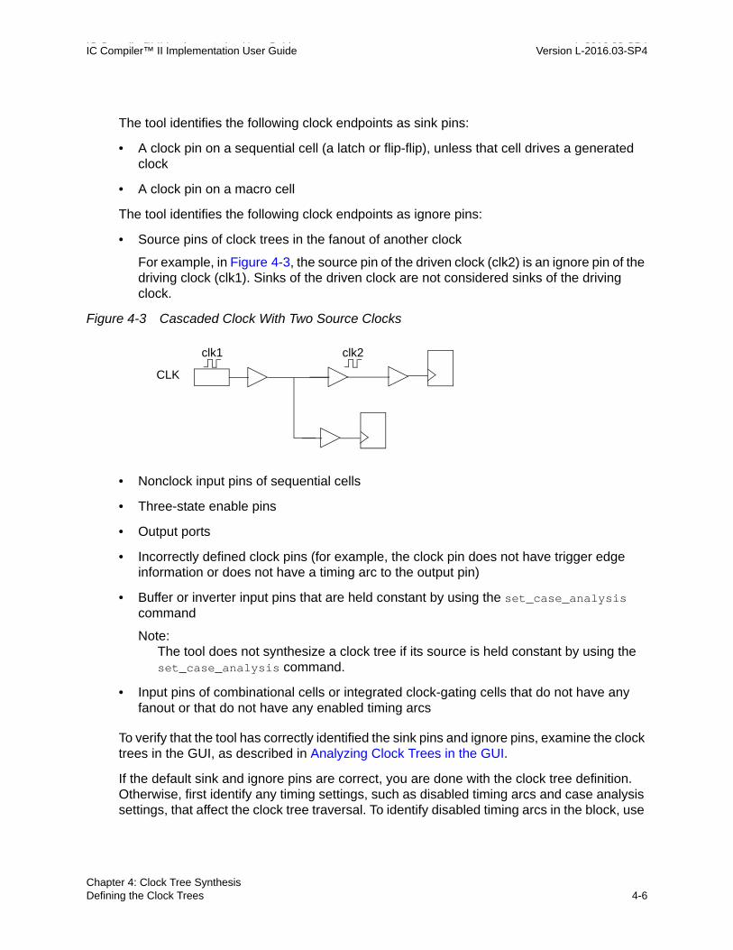
IC Compiler™ II Implementation User Guide L-2016.03-SP4IC Compiler™ II Implementation User Guide Version L-2016.03-SP4
The tool identifies the following clock endpoints as sink pins:
• A clock pin on a sequential cell (a latch or flip-flip), unless that cell drives a generated clock
• A clock pin on a macro cell
The tool identifies the following clock endpoints as ignore pins:
• Source pins of clock trees in the fanout of another clock
For example, in Figure 4-3, the source pin of the driven clock (clk2) is an ignore pin of the driving clock (clk1). Sinks of the driven clock are not considered sinks of the driving clock.
Figure 4-3 Cascaded Clock With Two Source Clocks
• Nonclock input pins of sequential cells
• Three-state enable pins
• Output ports
• Incorrectly defined clock pins (for example, the clock pin does not have trigger edge information or does not have a timing arc to the output pin)
• Buffer or inverter input pins that are held constant by using the set_case_analysis command
Note: The tool does not synthesize a clock tree if its source is held constant by using the set_case_analysis command.
• Input pins of combinational cells or integrated clock-gating cells that do not have any fanout or that do not have any enabled timing arcs
To verify that the tool has correctly identified the sink pins and ignore pins, examine the clock trees in the GUI, as described in Analyzing Clock Trees in the GUI.
If the default sink and ignore pins are correct, you are done with the clock tree definition. Otherwise, first identify any timing settings, such as disabled timing arcs and case analysis settings, that affect the clock tree traversal. To identify disabled timing arcs in the block, use
CLK
clk1 clk2
Chapter 4: Clock Tree SynthesisDefining the Clock Trees 4-6
IC Compiler™ II Implementation User Guide Version L-2016.03-SP4
the report_disable_timing command. To identify case analysis settings in the block, use the report_case_analysis command. Remove any timing settings that cause an incorrect clock tree definition.
If necessary, you can override the default balancing and ignore pin settings by using the set_clock_balance_points command, as described in Defining Clock Tree Exceptions.
Defining Clock Tree Exceptions
Clock tree exceptions are user-defined changes to the default endpoints (balancing and ignore pins) derived by the tool for a specific clock or to the treatment of portions of a clock tree during clock tree synthesis.
The IC Compiler II tool supports the following types of clock tree exceptions:
• User-defined sink pins
These exceptions define sink pins in addition to those derived by the tool for a clock tree. For example, you might define a tool-derived ignore pin as a clock sink.
For information about defining sink pins, see Defining Sink Pins.
• User-defined insertion delay requirements
These exceptions specify special insertion delay requirements for a sink pin (either derived or user-specified).
For information about defining insertion delay requirements, see Defining Insertion Delay Requirements.
• User-defined ignore pins
These exceptions exclude clock endpoints that were derived as sink pins by the tool. For example, you might define an ignore pin to exclude all branches of the clock tree that fan out from some combinational logic or to exclude a tool-derived sink pin.
For information about defining ignore pins, see Defining Ignore Pins.
• Don’t touch exceptions
These exceptions identify parts of the clock tree on which clock tree synthesis and optimization is not performed. You can use don’t touch exceptions to prevent the modification of a clock network beyond a specific pin, the buffering of specific nets, or the sizing of specific cells.
For information about defining don’t touch exceptions, see Setting Don’t Touch Exceptions.
Chapter 4: Clock Tree SynthesisDefining the Clock Trees 4-7Chapter 4: Clock Tree SynthesisDefining the Clock Trees 4-7

IC Compiler™ II Implementation User Guide L-2016.03-SP4IC Compiler™ II Implementation User Guide Version L-2016.03-SP4
• Size-only exceptions
These exceptions identify clock tree cells for which the tool can perform only cell sizing. Note that these cells can be moved, unless they have a placement status of fixed.
For information about defining size-only exceptions, see Setting Size-Only Exceptions.
Defining Sink Pins
To define one or more pins as sink pins, use the following syntax:
set_clock_balance_points-clock clock-consider_for_balancing true-balance_points pins[-corners corners]
The -clock option is not required. If you do not use it, the sink pin applies to all clocks.
By default, the insertion delay for the user-specified sink pins is 0. For information about overriding the default insertion delay, see Defining Insertion Delay Requirements.
When you define sink pins, by default, they apply to all corners. To apply the definition to specific corners, use the -corners option.
For example, to specify pin U2/A as a sink pin for the CLK clock in the current corner, use the following command:
icc2_shell> set_clock_balance_points -clock [get_clocks CLK] \-consider_for_balancing true -balance_points [get_pins U2/A]
To report the user-defined sink pins, use the report_clock_balance_points command. This command reports both the user-defined sink pins and the user-defined ignore pins.
To remove the sink pin definition from a pin, use the remove_clock_balance_points command.
For example, to remove the sink pin definition from the U2/A pin for the CLK clock, use the following command:
icc2_shell> remove_clock_balance_points -clock [get_clocks CLK] \-balance_points [get_pins U2/A]
Defining Insertion Delay Requirements
To override the default phase delay of zero for sink pins (derived or user-specified), use the -delay option with the set_clock_balance_points command to specify the insertion delay requirements. The tool adds the specified delay (positive or negative) to the calculated insertion delay up to the specified sink pin.
Chapter 4: Clock Tree SynthesisDefining the Clock Trees 4-8

IC Compiler™ II Implementation User Guide Version L-2016.03-SP4
The syntax to define the insertion delay requirement for one or more sink pins is
set_clock_balance_points[-clock clock]-delay delay [-rise] [-fall] [-early] [-late]-balance_points pins[-corners corners]
The -clock option is not required. If you do not use it, the insertion delay requirement applies to all clocks.
Clock tree synthesis uses the specified delay value for the path delay calculations used to build the clock tree. By default, the specified delay value is used for both longest-path and shortest-path calculations for both rising-edge and falling-edge paths. To control when the specified delay value is used, use the -rise, -fall, -early, and -late options.
When you define insertion delay requirements, by default, they apply to all corners. To apply the definition to specific corners, use the -corners option.
For example, to specify that clock tree synthesis should use an insertion delay of 2.0 ns for rising-edge shortest-path calculations for the U2/CLK pin for the CLK clock in the current corner, use the following command:
icc2_shell> set_clock_balance_points -clock [get_clocks CLK] \-rise -early -delay 2.0 -balance_points [get_pins U2/CLK]
To report the user-defined insertion delay for sink pins, use the report_clock_balance_points command. This command reports the user-defined sink pins, the derived sink pins with user-specified insertion delay, and the user-defined ignore pins.
Defining Ignore Pins
To define one or more pins as ignore pins, use the following syntax:
set_clock_balance_points[-clock clock]-consider_for_balancing false-balance_points pins
The -clock option is not required. If you do not use it, all user-defined ignore pins apply to all clocks.
For example, to exclude clock sink U2/CLK from the CLK clock, use the following command:
icc2_shell> set_clock_balance_points -clock [get_clocks CLK] \-consider_for_balancing false -balance_points [get_pins U2/CLK]
Chapter 4: Clock Tree SynthesisDefining the Clock Trees 4-9Chapter 4: Clock Tree SynthesisDefining the Clock Trees 4-9

IC Compiler™ II Implementation User Guide L-2016.03-SP4IC Compiler™ II Implementation User Guide Version L-2016.03-SP4
For another example, assume that a clock tree also drives combinational logic, as shown in Figure 4-4.
Figure 4-4 User-Defined Ignore Pin
To exclude all branches of the CLK clock tree that fan out from this point, use the following command:
icc2_shell> set_clock_balance_points -clock [get_clocks CLK] \-consider_for_balancing false -balance_points [get_pins U2/A]
To report the user-defined ignore pins, use the report_clock_balance_points command. This command reports both the user-defined sink pins and the user-defined ignore pins.
To remove the ignore pin definition from a pin, use the remove_clock_balance_points command.
For example, to remove the ignore pin definition from pin U2/CLK for the CLK clock, use the following command:
icc2_shell> remove_clock_balance_points -clock [get_clocks CLK] \-balance_points [get_pins U2/CLK]
Setting Don’t Touch Exceptions
To set a don't touch exception on a clock tree, use the set_dont_touch_network command.
icc2_shell> set_dont_touch_network -clock_only [get_pins pin_name]
The -clock_only option sets the don't touch exception only on the clock network. If you do not specify the -clock_only option, the don't touch exception is set on both the data path and the clock path.
CLK
A
BU2
n1
Chapter 4: Clock Tree SynthesisDefining the Clock Trees 4-10

IC Compiler™ II Implementation User Guide Version L-2016.03-SP4
To remove the don't touch exception from a clock tree, use the -clear option with the set_dont_touch_network command.
icc2_shell> set_dont_touch_network -clock_only [get_pins pin_name] -clear
You can also set don't touch exceptions on specific objects in the clock network by using the set_dont_touch command.
The following commands set a don't touch exception on a cell and a net:
icc2_shell> set_dont_touch [get_cells cell_name] true icc2_shell> set_dont_touch [get_nets -segments net_name] true
To report all the don't touch exceptions set on the current block, use the report_dont_touch command.
icc2_shell> report_dont_touch -all
Note: If a cell has a placement status of fixed, it is treated like a don’t touch cell during clock tree synthesis.
Setting Size-Only Exceptions
To set a size-only exception on a cell, use the set_size_only command.
The following command sets a size-only exception on a cell:
icc2_shell> set_size_only [get_cells cell_name] true
To report all the size-only exceptions set on the current block, use the report_size_only command.
icc2_shell> report_size_only -all
See Also
• Querying and Changing the Placement Status
• Setting Don’t Touch Exceptions
• Restricting Optimization on Cells
Chapter 4: Clock Tree SynthesisDefining the Clock Trees 4-11Chapter 4: Clock Tree SynthesisDefining the Clock Trees 4-11

IC Compiler™ II Implementation User Guide L-2016.03-SP4IC Compiler™ II Implementation User Guide Version L-2016.03-SP4
Copying Clock Tree Exceptions Across Modes
You can specify that the tool copies clock tree exceptions from one mode to one or more equivalent modes by using the set_clock_tree_options command with the -copy_exceptions_across_modes, -from_mode, and -to_mode options.
The following example specifies that during clock tree synthesis the clock tree exceptions in the mode name M1 should be copied to the modes name M2 and M3:
icc2_shell> set_clock_tree_options -copy_exceptions_across_modes \ -from_mode M1 -to_mode {M2 M3}
Deriving Clock Tree Exceptions From Ideal Clock Latencies
If you have set ideal clock latencies for specific sinks in your design, you can use the derive_clock_balance_points command to convert these ideal latency settings to clock tree exceptions.
The derive_clock_balance_points command converts ideal latencies specified with the set_clock_latency command on clock sink pins to set_clock_balance_points commands. Use the derive_clock_balance_points command before clock tree synthesis, when the design has ideal clocks.
By default, the derive_clock_balance_points command
• Generates balance point constraints for all ideal primary clocks of all active scenarios that are enabled for setup analysis, hold analysis, or both. It does not generate balance points for generated clocks.
To generate the balance points for
❍ Specific primary clocks, use the -clocks option.
❍ All active scenarios of specific corners, use the -corners option.
• Calculates a reference latency for each primary ideal clock, which is the sum of the ideal source and network latency specified on the clock with the set_clock_latency command.
To specify a different reference latency value, use the -reference_latency option.
• Applies the derived clock balance point constraints to the design.
To generate an output file containing set_clock_balance_points commands, instead applying it to the design, use the -output option.
Balance points that the tool derives are clock and corner specific. Ensure that appropriate set_clock_latency constraints are set for all clocks for all modes used for clock tree synthesis in at least the worst corner.
Chapter 4: Clock Tree SynthesisDefining the Clock Trees 4-12

IC Compiler™ II Implementation User Guide Version L-2016.03-SP4
The tool uses the following formula to derive the delay values for the corresponding set_clock_balance_points commands:
(Clock balance point delay value at the sink) =
(Reference latency of the clock) - (Total ideal clock latency at the sink)
The total ideal clock latency at the sink is the sum of the source latency of the clock and the ideal network latency for the sink.
For example, assume you have the following timing constraint settings:
icc2_shell> set_clock_latency -source 0.5 [get_clocks clk]icc2_shell> set_clock_latency 1.0 [get_clocks clk]icc2_shell> set_clock_latency 1.5 [get_pin reg1/CK]icc2_shell> set_clock_latency 0.5 [get_pin reg2/CK]
If you run the derive_clock_balance_points command, the tool derives the following clock balance point constraints:
icc2_shell> set_clock_balance_points -delay -0.5 \-balance_points [get_pin reg1/CK] -clock clk –corner worst
icc2_shell> set_clock_balance_points -delay 0.5 \-balance_points [get_pin reg2/CK] -clock clk –corner worst
To avoid conflicts, do not manually apply any clock balance points for a clock that you derive balance points with the derive_clock_balance_points command.
Handling Endpoints With Balancing Conflicts
In some blocks, the clocks have endpoints that are structurally impossible to balance. The IC Compiler II tool can automatically detect endpoints with balancing conflicts and derive an ignore pin to resolve the conflict. This capability is enabled by default for the synthesize_clock_trees and clock_opt commands. To disable this capability, set the cts.common.enable_auto_exceptions application option to false.
With this capability, the tool detects and fixes the following types of balancing conflicts:
• Internal sink pins of modules that have a combinational clock path
If a module contains both internal sink pins and combinational clock paths, it is impossible to balance the internal sink pins. To resolve the balancing conflict, the tool defines the internal sink pins as ignore pins.
For example, assume that you have a module that contains a combinational path in the clock network, as shown in figure (a) in Figure 4-5, which is represented by the extracted timing model (ETM) shown in figure (b).
Chapter 4: Clock Tree SynthesisDefining the Clock Trees 4-13Chapter 4: Clock Tree SynthesisDefining the Clock Trees 4-13

IC Compiler™ II Implementation User Guide L-2016.03-SP4IC Compiler™ II Implementation User Guide Version L-2016.03-SP4
Figure 4-5 Module With Combinational Clock Path
In this case, the internal check pin inside the ETM has delays coming from the ETM timing library; these delays are considered by clock tree synthesis as sinks and are balanced with other sinks at the top level. If the path to the check pin is the shortest path, top-level clock tree synthesis cannot insert buffers on the shortest path and therefore leaves a large skew at the top level. Setting the internal check pin as an ignore pin resolves the skew issue coming from the ETM.
• Sink pins that cannot be balanced simultaneously
If a block contains two clocks that drive common sinks, one of which is a clock pin that is the parent of another sink, due to a generated clock, it is impossible to simultaneously balance the parent and child clock pins with another common sink. To resolve the balancing conflict, the tool defines the parent clock pin as an ignore pin.
For example, in Figure 4-6, FF_gen/CLK and FF0_1-10/CLK are sinks of clkb, FF1_1-10/CLK and FF0_1-10/CLK are sinks of clka, and FF_gen/CLK is the parent of FF1_1-10/CLK. In this case, the tool defines FF_gen/CLK as an ignore pin for clkb to resolve the balancing conflict.
Q
Clk_out
D
Clk
(a) Netlist (b) ETM with check pin
Clk
D Q
Clk_out
Clk_check_pin_1
Combinational delay
Chapter 4: Clock Tree SynthesisDefining the Clock Trees 4-14

IC Compiler™ II Implementation User Guide Version L-2016.03-SP4
Figure 4-6 Clock Pins That Cannot Be Balanced Simultaneously
Verifying the Clock Trees
Before you synthesize the clock trees, use the check_clock_trees command to verify that the clock trees are properly defined. For example, to verify that the CLK clock tree is properly defined, use the following command:
icc2_shell> check_clock_trees -clocks [get_clocks CLK]
If you do not specify the -clock option, the tool checks all clocks in the current block.
The check_clock_trees command checks for the following issues:
• Clock (master or generated) with no sinks
• Loops in the clock network
• Multiple clocks reach the same register because of overlapping clocks, but multiple-clocks-per-register propagation is not enabled
• Ignored clock tree exceptions
• Stop pin or float pin defined on an output pin
• Buffers with multiple timing arcs used in clock tree references
• Situations that cause an empty buffer list
Chapter 4: Clock Tree SynthesisVerifying the Clock Trees 4-15Chapter 4: Clock Tree SynthesisVerifying the Clock Trees 4-15

IC Compiler™ II Implementation User Guide L-2016.03-SP4IC Compiler™ II Implementation User Guide Version L-2016.03-SP4
• Generated clock without a valid master clock source
A generated clock does not have a valid master-clock source in the following situations:
❍ The master clock specified in create_generated_clock does not exist
❍ The master clock specified in create_generated_clock does not drive the source pin of the generated clock
❍ The source pin of the generated clock is driven by multiple clocks, and some of the master clocks are not specified with create_generated_clock.
For example, in Figure 4-7, the GEN_REG/Q pin is driven by both CLKA and CLKB. If only CLKA is specified as a master clock in a create_generated_clock command, GEN_CLK does not have a valid master clock source.
Figure 4-7 Generated Clock With Invalid Master Clock Source
For multicorner-multimode designs, the check_clock_trees command checks all active scenarios for the following issues:
• Conflicting per-clock exception settings
• Conflicting balancing settings
Before you implement the clock trees, you should manually fix the reported issues. Each message generated by the check_clock_trees command has a detailed man page that describes how to fix the identified issue. You can improve the clock tree and timing QoR by fixing all the issues identified by the check_clock_trees command.
D Q
0
1
REG1
REG2
D Q
D Q
GEN_REG
CLKA
CLKB
GEN_CLK
Chapter 4: Clock Tree SynthesisVerifying the Clock Trees 4-16

IC Compiler™ II Implementation User Guide Version L-2016.03-SP4
Setting Clock Tree Design Rule Constraints
The IC Compiler II tool supports the following design rule constraints for clock tree synthesis:
• Maximum capacitance
To specify maximum capacitance constraints for clock tree synthesis, use the -clock_path option with the set_max_capacitance command.
If you do not specify this constraint, the clock tree synthesis default is 0.6 pF.
• Maximum transition time
To specify maximum transition time constraints for clock tree synthesis, use the -clock_path option with the set_max_transition command.
If you do not specify this constraint, the clock tree synthesis default is 0.5 ns.
By default, these constraints apply to all corners associated with the current mode. To set the constraint for a specific mode, use the -mode option with the get_clocks command to identify the clocks. To set the constraint for specific corners associated with the specified mode, use the -corners option with the constraint command. Be careful to apply the correct constraints across all the modes and their associated corners.
For example, to set a maximum transition time of 0.20 ns on all pins in the CLK clock path for all corners of the current mode, use the following command:
icc2_shell> set_max_transition 0.20 -clock_path [get_clocks CLK]
To set different maximum transition time constraints for different corners associated with a specific mode, use the -mode option with the get_clocks command to specify the mode and use the -corners option to specify the corner.
For example, to set the maximum transition time to 0.15 ns for corner1 in mode1 and 0.10 ns for corner2 in mode1, use the following commands:
icc2_shell> set_max_transition 0.15 -corners corner1 \-clock_path [get_clocks -mode mode1]
icc2_shell> set_max_transition 0.10 -corners corner2 \-clock_path [get_clocks -mode mode1]
To set the same maximum capacitance constraint for different corners associated with a specific mode, use the following command:
icc2_shell> set_max_capacitance 0.6 \ -clock_path [get_clocks -mode mode2] \
-corners [get_corner \[get_attribute [get_mode mode2] associated_corners]]
Chapter 4: Clock Tree SynthesisSetting Clock Tree Design Rule Constraints 4-17Chapter 4: Clock Tree SynthesisSetting Clock Tree Design Rule Constraints 4-17

IC Compiler™ II Implementation User Guide L-2016.03-SP4IC Compiler™ II Implementation User Guide Version L-2016.03-SP4
Specifying the Clock Tree Synthesis Settings
The clock tree synthesis options guide the implementation of the clock trees. The following topics describe how to set these options:
• Specifying the Clock Tree References
• Setting Skew and Latency Targets
• Enabling Local Skew Optimization
• Specifying the Primary Corner for Clock Tree Synthesis
• Preserving Preexisting Clock Trees
• Preserving the Clock Ports of Existing Hierarchies
• Reducing Electromigration
• Handling Inaccurate Constraints During Clock Tree Synthesis
• Defining Clock Cell Spacing Rules
• Creating Skew Groups
• Defining a Name Prefix for Clock Cells
• Using the Global Router During Initial Clock Tree Synthesis
• Setting Clock Tree Routing Options
• Reporting the Clock Tree Settings
Specifying the Clock Tree References
The buffer and inverter cells that can be used to build a clock tree and the reference cells of the preexisting gates of the clock tree are referred to as clock tree references. To specify the clock tree references, use the set_lib_cell_purpose -include cts command.
Ensure that the list of cells you specify as clock tree references meets the following criteria:
• The list contains at least one buffer or one inverter
• The list contains the library cells of the preexisting gates
If they are not included in the list, the tool is unable to resize these preexisting gates during clock tree synthesis and optimization. You can automatically derive equivalent cells for all the preexisting clock tree cells that are not buffers or inverters and specify them as clock references by using the derive_clock_cell_references command, as described in Deriving Clock Tree References for Preexisting Gates.
Chapter 4: Clock Tree SynthesisSpecifying the Clock Tree Synthesis Settings 4-18
IC Compiler™ II Implementation User Guide Version L-2016.03-SP4
• For multivoltage designs with always-on buffering requirements, the list contains always-on cells
• The library cells in the reference list do not have a dont_touch attribute
If library cells have the dont_touch attribute set on them, they are not used by clock tree synthesis even if you specify them as clock tree references.
To ensure that clock tree synthesis uses only the specified set of cells and that these cells are not used by any optimization step other than clock tree synthesis, run the following commands:
icc2_shell> set cts_cells list_of_cellsicc2_shell> set_lib_cell_purpose -exclude cts [get_lib_cells] icc2_shell> set_lib_cell_purpose -include none [get_lib_cells $cts_cells]icc2_shell> set_lib_cell_purpose -include cts [get_lib_cells $cts_cells]
Deriving Clock Tree References for Preexisting Gates
To ensure that the tool resize preexisting gates in the clock network during clock tree synthesis and optimization, you must specify equivalent cells as clock references. Not specifying a complete list of equivalent cells for preexisting gates can affect clock tree QoR.
You can automatically derive equivalent cells for all the preexisting clock tree cells and specify them as clock references by using the derive_clock_cell_references command.
When you run this command, the tool sets the valid_purpose attribute to true on equivalent library cells of the preexisting clock tree cells that are not buffers or inverters. This command does not derive equivalent library cells for preexisting buffers and inverters, Therefore, you must manually specify the buffers and inverters to use for clock tree synthesis, as shown in the following example:
icc2_shell> set_lib_cell_purpose –include cts \{tech_lib/clk_buf* tech_lib/clk_inv*}
icc2_shell> derive_clock_cell_referencesicc2_shell> synthesize_clock_trees
Instead of automatically specifying the equivalent library cells of the preexisting clock tree cells as clock tree references, you can generate a Tcl script that specifies the equivalent library cells of the preexisting clock tree cells as clock tree references. To do so, use the -output option.
icc2_shell> derive_clock_cell_references -output cts_leq_cells.tcl
Chapter 4: Clock Tree SynthesisSpecifying the Clock Tree Synthesis Settings 4-19Chapter 4: Clock Tree SynthesisSpecifying the Clock Tree Synthesis Settings 4-19

IC Compiler™ II Implementation User Guide L-2016.03-SP4IC Compiler™ II Implementation User Guide Version L-2016.03-SP4
You can edit the output file, source it, and then run clock tree synthesis, as shown in the following example:
icc2_shell> set_lib_cell_purpose –include cts \{tech_lib/clk_buf* tech_lib/clk_inv*}
icc2_shell> source cts_leq_cells.tclicc2_shell> synthesize_clock_trees
Restricting the Target Libraries Used
You can restrict the libraries used during clock tree synthesis for the top level or a lower level of the logical hierarchy of a design by using the set_target_library_subset -clock command. To enable the use of the target library subset, you must set the opt.common.enable_target_library_subset_opt application option to 1.
The following example specifies the buf1 and buf2 cells from the HVT_lib and LVT_lib libraries as clock tree references. However, it restricts the lower-level block named TSK_BLK to use only the cells from the LVT_lib library for its clock nets. Therefore, only buf1 and buf2 cells from the LVT_lib library are used as clock references for that block.
icc2_shell> set_lib_cell_purpose -include cts \{HVT_lib/buf1 HVT_lib/buf2 LVT_lib/buf1 LVT_lib/buf2}
icc2_shell> set_target_library_subset -clock {LVT_lib} \-objects [TOP/TSK_BLK]
icc2_shell> set_app_options \ -name opt.common.enable_target_library_subset_opt -value 1
See Also
• Restricting Library Cell Usage
• Restricting the Target Libraries Used
Setting Skew and Latency Targets
By default, clock tree synthesis tries to achieve the best skew and latency for all clocks. However, this can lead to area, power, and runtime overhead for low frequency clocks, which have relaxed skew and latency targets.
• To specify a skew target, use the -target_skew option with the set_clock_tree_options command.
• To specify a latency target, use the -target_latency option with the set_clock_tree_options command.
By default, when you define skew and latency targets, they apply to all clocks in all corners. To define targets for specific clocks, use the -clocks option. To define targets for specific corners, use the -corners option.
Chapter 4: Clock Tree SynthesisSpecifying the Clock Tree Synthesis Settings 4-20
IC Compiler™ II Implementation User Guide Version L-2016.03-SP4
To report the user-defined skew and latency targets, use the report_clock_tree_options command.
To remove user-defined skew or latency targets, use the remove_clock_tree_options command. To remove all skew and latency targets, use the -all option; otherwise, use the appropriate -target_skew, -target_latency, -clocks, and -corners options to remove the specific targets.
Enabling Local Skew Optimization
During clock tree synthesis, by default, the tool tries to minimize the global skew, which is the difference between the longest and shortest clock paths. If there is no timing path between the registers with the longest and shortest clock paths, optimizing global skew does not improve the timing QoR of the design. However, by optimizing the local skew, which is the worst skew between launch and capture registers of timing paths, you can improve the timing QoR of the design. During local skew optimization, the tool works on improving local skew of all violating setup and hold timing paths.
To enable local skew optimization during the clock tree synthesis and clock tree optimization stages of the synthesize_clock_trees and clock_opt commands, set the cts.compile.enable_local_skew and cts.optimize.enable_local_skew application options to true.
icc2_shell> set_app_options -list {cts.compile.enable_local_skew true}icc2_shell> set_app_options -list {cts.optimize.enable_local_skew true}
When you enable local skew optimization using the previous settings, by default, the tool derives skew targets that help improve the timing QoR, and ignores the target skew you specify with the set_clock_tree_options -target_skew command. To prevent the tool from deriving skew targets, use the following application option setting:
icc2_shell> set_app_options \ -list {cts.common.enable_auto_skew_target_for_local_skew false}
Specifying the Primary Corner for Clock Tree Synthesis
During initial clock tree synthesis, by default, the tool identifies the corner with the worst clock delays and inserts buffers to balance the clock delays in all modes of this corner. To identify a specific corner as the primary corner for initial clock tree synthesis, use the cts.compile.primary_corner application option.
Chapter 4: Clock Tree SynthesisSpecifying the Clock Tree Synthesis Settings 4-21Chapter 4: Clock Tree SynthesisSpecifying the Clock Tree Synthesis Settings 4-21

IC Compiler™ II Implementation User Guide L-2016.03-SP4IC Compiler™ II Implementation User Guide Version L-2016.03-SP4
Preserving Preexisting Clock Trees
When you perform clock tree synthesis, by default, the tool removes all preexisting clock buffers and inverters. You can prevent this by setting the cts.compile.remove_existing_clock_trees application option to false.
To preserve specific preexisting clock buffers or inverters, apply a don’t touch or size-only exception on them.
Preserving the Clock Ports of Existing Hierarchies
By default, clock tree synthesis can create new clock ports on existing hierarchical cells when buffering hierarchical clock nets. To prevent the creation of additional clock ports on hierarchical cells, use the set_freeze_ports command to set the freeze_clock_port attribute on the cells to true.
For example, to prevent the creation of additional clock ports on the I1 cell instance, use the following command:
icc2_shell> set_freeze_ports -clock [get_cells I2] true
To report the freeze-port settings, use the report_freeze_ports command. To report the settings for all instances, use the -all option; to report the settings for specific instances, specify the instances using a Tcl list or collection.
Reducing Electromigration
Clock cells consume more power than cells that are not in the clock network. Clock cells that are clustered together in a small area increase the current densities for the power and ground rails, which increases the potential for electromigration problems. One way to avoid the problem is to set spacing requirements between clock cells to prevent local clumping of the clock cells along a standard cell power rail between the perpendicular straps.
To use this method to reduce electromigration in the block,
1. Define clock cell spacing rules for the inverters, buffers, and integrated clock-gating cells in the clock network by using the set_clock_cell_spacing command, as described in Defining Clock Cell Spacing Rules.
2. Perform clock tree synthesis by using the synthesize_clock_trees command, as described in Performing Standalone Clock Trees Synthesis, or the clock_opt command, as described in Synthesizing and Routing Clock Trees, and Optimizing the Design With a Single Command.
Chapter 4: Clock Tree SynthesisSpecifying the Clock Tree Synthesis Settings 4-22

IC Compiler™ II Implementation User Guide Version L-2016.03-SP4
Note: The clock cell spacing rules are also honored by the balance_clock_groups command. For information about using this command, see Balancing Skew Between Different Clock Trees.
3. Check clock cell spacing rule violations by using the check_legality -verbose command.
You should not see any violations if you set the appropriate clock cell spacing constraints.
Handling Inaccurate Constraints During Clock Tree Synthesis
In the early stages of the implementation of a design, the constraints can be inaccurate or too restrictive. Running clock tree synthesis on such a design can lead to long runtime or poor clock tree QoR.
You can run clock tree synthesis on such a design, but still get usable results in a reasonable runtime. To do so, set the following application variable before you begin clock tree synthesis:
icc2_shell> set_app_options –list \ {cts.common.enable_dirty_design_mode true}
When you use this application option setting, the tool
• Ignores dont_touch and dont_touch_network attribute settings on clock nets.
• Removes maximum transition and maximum capacitance constraints if they are too tight.
• Removes the maximum net length constraint if it is less than 50 microns.
• Ignores clock cell spacing rules if the horizontal spacing requirement is more than three times the site height and the vertical spacing requirement is more than twenty times the site height.
• Ignores nondefault routing rules if the width plus the spacing requirement of the routing rule is more than ten times the default width plus the default spacing.
• Reports balance point delay values that are large enough to cause an increase in clock insertion delay.
Chapter 4: Clock Tree SynthesisSpecifying the Clock Tree Synthesis Settings 4-23Chapter 4: Clock Tree SynthesisSpecifying the Clock Tree Synthesis Settings 4-23

IC Compiler™ II Implementation User Guide L-2016.03-SP4IC Compiler™ II Implementation User Guide Version L-2016.03-SP4
Defining Clock Cell Spacing Rules
To define clock cell spacing rules, use the set_clock_cell_spacing command. At a minimum, you must specify the minimum spacing in the x-direction or the y-direction; typically you would specify the minimum spacing in both directions.
To specify the minimum spacing in microns in the
• X-direction, set the -x_spacing option to a nonzero value
This value is usually dependent on the library cell’s drive strength and clock frequency.
• Y-direction, set the -y_spacing option to a nonzero value
This value is usually less than half a row height.
Note: Using a large spacing value increases the skew because the cells are spaced further away from the intended clusters of sinks.
By default, the specified cell spacing requirements apply to all clock cells. To restrict the clock cell spacing rules to specific
• Library cells, use the -lib_cells option
• Clocks, use the -clocks option
If adjoining clock cells both have cell spacing rules for a given direction, the sum of the spacing values applies. For example, if two adjoining clock cells both have a minimum cell spacing of 5 microns in the x-direction, they are placed at least 10 microns apart in the x-direction. You can relax the adjoining cell spacing rule by setting the cts.placement.cell_spacing_rule_style application option to maximum, in which case the tool uses the larger of the spacing settings between two adjoining cells instead of the sum of the spacing settings. For example, the clock cells in the previous example are placed at least 5 microns apart in the x-direction, instead of 10 microns.
The clock cell spacing rules defined by the set_clock_cell_spacing command are honored by the synthesize_clock_trees, balance_clock_groups, and clock_opt commands.
To report clock cell spacing rules, use the report_clock_cell_spacings command.
To remove clock cell spacing rules, use the remove_clock_cell_spacings command. By default, this command removes all clock cell spacing rules. To remove specific clock cell spacing rules, use the -lib_cells option.
Chapter 4: Clock Tree SynthesisSpecifying the Clock Tree Synthesis Settings 4-24
IC Compiler™ II Implementation User Guide Version L-2016.03-SP4
Creating Skew Groups
During clock tree synthesis, you might want to balance a group of sinks only among each other, and not the rest of the sinks. To do so, define a skew group by using the create_clock_skew_group command.
When you use this command, specify the sinks you want to group, by using the -objects option.
Optionally, you can specify:
• A mode for which to create the skew group.
By default, the tool create the skew group for the current mode.
• A name for the skew group by using the -name option
The following example creates a skew group named sg1 consisting of sinks reg1/CP, reg2/CP, and reg3/CP:
icc2_shell> create_clock_skew_group -name sg1 \ -objects {reg1/CP reg2/CP reg3/CP}
To report skew groups, use the report_clock_skew_groups command. To remove skew groups, use the remove_clock_skew_groups command.
Defining a Name Prefix for Clock Cells
You can specify a name prefix for the cells added on the clock network during clock tree synthesis by using the cts.common.user_instance_name_prefix application option.
The following example specifies CTS_ as the name prefix for the cells added on the clock network during clock tree synthesis:
icc2_shell> set_app_options \ -name cts.common.user_instance_name_prefix -value "CTS_"
To specify a name prefix for the cells added on the data nets during optimization, including during the clock_opt command, use the opt.common.user_instance_name_prefix application option, as described in Defining a Cell Name Prefix for Optimization.
Chapter 4: Clock Tree SynthesisSpecifying the Clock Tree Synthesis Settings 4-25Chapter 4: Clock Tree SynthesisSpecifying the Clock Tree Synthesis Settings 4-25

IC Compiler™ II Implementation User Guide L-2016.03-SP4IC Compiler™ II Implementation User Guide Version L-2016.03-SP4
Using the Global Router During Initial Clock Tree Synthesis
By default, initial clock tree synthesis uses the virtual router to build the clock trees. For designs with complex floorplans, this can introduce congestion hotspots and degrade clock QoR after clock routing.
The tool can use the global router during the initial clock tree synthesis stage of the synthesize_clock_trees and clock_opt commands. To enable this feature, set the cts.compile.enable_global_route application option to true.
Setting Clock Tree Routing Options
By default, the IC Compiler II tool uses the default routing rule and any available routing layers to route the clock trees. To reduce the wire delays in the clock trees, you can use wide wires and higher metal layers instead. Wide wires are represented by nondefault routing rules. To use nondefault routing rules on the clock nets, you must first define the routing rules and then assign them to the clock nets, as described in Using Nondefault Routing Rules.
Reducing Signal Integrity Effects on Clock Nets
The timing of a design can be improved by reducing signal integrity issues on clock nets. To do so, the tool can derive nondefault routing rules with larger spacing requirements and assign them to the clock nets in regions without routing congestion.
To enable this feature, use the following application option setting:
icc2_shell> set_app_options -list \{cts.optimize.enable_congestion_aware_ndr_promotion true}
When the tool derives a new nondefault routing rule for a clock net, the new spacing requirement is dependent on the spacing requirement of the existing routing rule of that net. If the existing routing rule is
• A nondefault routing rule with a spacing requirement of less than or equal to two times the default spacing, the spacing requirement is doubled
The name of this new nondefault rule is the original name with an _ext_spacing postfix.
• A nondefault routing rule with a spacing requirement of more than two times the default spacing, the spacing requirement is increased by one default spacing
The name of this new nondefault rule is the original name with an _ext_spacing postfix.
• The default routing rule, the spacing requirement is doubled
The name of this new nondefault rule is default_rule_equivalent_ndr_double_spacing.
Chapter 4: Clock Tree SynthesisSpecifying the Clock Tree Synthesis Settings 4-26
IC Compiler™ II Implementation User Guide Version L-2016.03-SP4
Reporting the Clock Tree Settings
To report the settings that are used by clock tree synthesis, use the report_clock_settings command. By default, the commands reports the clock tree configuration, including the design rule constraints, target skew, and target latency; the clock tree references; the clock cell spacing rules; and the nondefault routing rules for all clocks in the current block.
To report the settings for specific clocks, use the -clock option to specify the clocks of interest. To report specific information, use the -type option with the appropriate keyword.
• To report the clock tree design rule constraints, target skew, and target latency, use -type configurations.
• To report the clock tree references, use -type references.
• To report the clock cell spacing rules, use -type spacing_rules.
• To report the nondefault routing rule used for the clock nets, use -type routing_rules.
Implementing Clock Trees
Before you perform clock tree synthesis, you should save the block. This allows you to refine the clock tree synthesis goals and rerun clock tree synthesis with the same starting point, if necessary.
The following topics describe the different methods available for implementing clock trees:
• Performing Standalone Clock Trees Synthesis
• Synthesizing and Routing Clock Trees, and Optimizing the Design With a Single Command
• Performing Concurrent Clock and Data Optimization
• Splitting Clock Cells
• Balancing Skew Between Different Clock Trees
• Optimizing the Design After Clock Tree Synthesis
• Routing Clock Trees
• Performing Postroute Clock Tree Optimization
• Marking Clock Trees as Synthesized
• Removing Clock Trees
Chapter 4: Clock Tree SynthesisImplementing Clock Trees 4-27Chapter 4: Clock Tree SynthesisImplementing Clock Trees 4-27

IC Compiler™ II Implementation User Guide L-2016.03-SP4IC Compiler™ II Implementation User Guide Version L-2016.03-SP4
Performing Standalone Clock Trees Synthesis
To perform standalone clock tree synthesis, use the synthesize_clock_trees command, as shown in the following example:
icc2_shell> synthesize_clock_trees
When you use this command, the tool performs the following tasks:
1. Clock tree synthesis
Before clock tree synthesis, the tool performs virtual routing of the clock nets and uses RC estimation to determine the clock net timing.
2. Clock tree optimization
Before clock tree optimization, the tool performs global routing on the clock nets and uses RC extraction to determine the clock net timing. During clock tree optimization, the tool performs incremental global routing on clock nets modified during optimization.
Note: This command does not detail route the clock trees.
By default, this command works on all clocks in all active scenarios that are enabled for setup or hold analysis. You can specify the clocks to be built by using the -clock option. For example, to build only the CLK clock tree, use the following command:
icc2_shell> synthesize_clock_trees -clocks [get_clocks CLK]
After clock tree synthesis, the tool sets the synthesized clocks in the active modes as propagated. If your block has modes that are not active for clock tree synthesis, set these modes as active and run the synthesize_clock_trees -propagate_only command after clock tree synthesis to set the clocks for these modes as propagated. This command only removes the ideal setting from the clocks; it does not perform clock tree synthesis.
Chapter 4: Clock Tree SynthesisImplementing Clock Trees 4-28

IC Compiler™ II Implementation User Guide Version L-2016.03-SP4
Synthesizing and Routing Clock Trees, and Optimizing the Design With a Single Command
To synthesize the clock tress, route the clock nets, and further optimize the design by using a single command, use the clock_opt command.
The clock_opt command consist of the following three stages:
1. The build_clock stage, during which the tool synthesizes and optimizes the clock trees for all clocks in the active modes in all active scenarios. After clock tree synthesis, the tool sets the synthesized clocks as propagated.
2. The route_clock stage, during which the tool detail routes the synthesized clock nets.
3. The final_opto stage, during which the tool further optimizes the design for timing, logical DRC violations, area, power, and routability.
When you run the clock_opt command, by default, the tool executes all three stages. However, you can limit it to one or more contiguous stages. Use the -from option to specify the stage from which you want to begin and the -to option to specify the stage after which you want to end. If you do not specify the -from option, the tool begins from the final_clock stage. Similarly, if you do not specify the -to option, the tool continues until the final_opto stage is completed.
For example, to synthesize and optimize the clock trees and detail route the clock nets only, limit the execution to the final_clock and route_clock stages by use the following command:
icc2_shell> clock_opt -to route_clock
To perform only post-clock optimization, limit the execution to the final_opto stage by using the following command:
icc2_shell> clock_opt -from final_opto
Chapter 4: Clock Tree SynthesisImplementing Clock Trees 4-29Chapter 4: Clock Tree SynthesisImplementing Clock Trees 4-29

IC Compiler™ II Implementation User Guide L-2016.03-SP4IC Compiler™ II Implementation User Guide Version L-2016.03-SP4
Performing Concurrent Clock and Data Optimization
Useful skew techniques improve the timing QoR by adjusting the clock arrival times to take advantage of the positive slack in the design. However, applying the useful skew technique while performing datapath optimization, which is referred to as concurrent clock and data (CCD) optimization, results in a bigger improvement in the timing QoR.
To enable concurrent clock and data optimization for the
• clock_opt command, set the clock_opt.flow.enable_ccd application option to true.
icc2_shell> set_app_options –name clock_opt.flow.enable_ccd \–value true
• route_opt command, set the route_opt.flow.enable_ccd application option to true.
icc2_shell> set_app_options –name route_opt.flow.enable_ccd \ –value true
icc2_shell> route_opt
You can control concurrent clock and data optimization that is performed during the clock_opt and route_opt commands as follows:
• To specify that the clock latencies of the boundary registers should not be adjusted, set the ccd.optimize_boundary_timing application option to false.
icc2_shell> set_app_options –name ccd.optimize_boundary_timing \ –value false
When you use this setting, you can specify a collection of ports to ignore during boundary register identification by using the ccd.ignore_ports_for_boundary_identification application option.
For example, to the ports named IND1 and IND2 during boundary register identification, use the following command:
icc2_shell> set_app_options \ –name ccd.ignore_ports_for_boundary_identification \ –value {IND1 IND2}
• To ignore a specific path group, use the ccd.skip_path_groups application option and specify the name of the path group you want ignored.
You can ignore a path group for all scenarios or a specific scenario. For example, to ignore the path group named CLK1 for all scenarios and CLK2 for the scenario named scnA, use the following command:
icc2_shell> set_app_options –name ccd.skip_path_groups \ –value {CLK1 {CLK2 scnA}}
Chapter 4: Clock Tree SynthesisImplementing Clock Trees 4-30

IC Compiler™ II Implementation User Guide Version L-2016.03-SP4
• To limit the amount by which clock latencies are
❍ Advanced, use the ccd.max_prepone application option
❍ Delayed, use the ccd.max_postpone application option
The following example sets a limit of 0.2 for advancing and 0.1 for delaying clock latencies:
icc2_shell> set_app_options –list {ccd.max_prepone 0.2}icc2_shell> set_app_options –list {ccd.max_postpone 0.1}
Splitting Clock Cells
You can manually split clock cells that have DRC violations by using the split_clock_cells -cells command, as shown in the following example:
icc2_shell> split_clock_cells -cells [get_cells U1/ICG*]
The tool does not split the specified cells if
• They do not have DRC violations
• They have don’t-touch, size-only, or fixed-placement attribute settings
• It is necessary to punch ports on the boundaries of power domains or blocks that have been identified with the set_freeze_ports command
After splitting a cell, the tool
• Names the new cells using the <original_cell_name>_split_<integer> naming convention
• Copies all the settings and constraints from the original cell to the newly created cells
Instead of specifying the cells to split, you can specify one or more collection of loads that are driven by the same driver by using the -loads option, as shown in the following example:
icc2_shell> set loads1 [get_pins I1/reg*/CK]icc2_shell> set loads2 [get_pins I2/reg*/CK]icc2_shell> split_clock_cells -loads [list $load1 $load2]
After splitting, each set of loads is driven by a newly created driver.
Chapter 4: Clock Tree SynthesisImplementing Clock Trees 4-31Chapter 4: Clock Tree SynthesisImplementing Clock Trees 4-31

IC Compiler™ II Implementation User Guide L-2016.03-SP4IC Compiler™ II Implementation User Guide Version L-2016.03-SP4
Balancing Skew Between Different Clock Trees
The IC Compiler II tool can automatically balance the skew between a group of clocks. The set of clocks considered during delay balancing is referred to as a clock balance group. You can define multiple clock balance groups. For each clock balance group, you can define a delay offset between the clocks. Together, the clock balance groups and their delay offset settings are referred to as interclock delay balancing constraints.
Note: The tool cannot balance skew between a generated clock and other clocks.
To balance multiple clocks, perform the following steps:
1. Generate the interclock delay balancing constraints either by
Manually defining the clock balance groups and their delay offsets, as described in Defining the Interclock Delay Balancing Constraints
Having the tool generate them as described in Generating Interclock Delay Balancing Constraints Automatically
2. Balance the interclock delays as described in Running Interclock Delay Balancing.
Defining the Interclock Delay Balancing Constraints
To define interclock delay balancing constraints, use the create_clock_balance_group command. At a minimum, you must specify a name for the clock balance group and the clocks in the group.
• To specify a name for the clock balance group, use the -name option.
• To specify the clock trees in the group, use the -objects option. By default, the clock balance group is defined for the current mode. To define a clock balance group for a specific mode, use the -mode option with the get_clocks command to specify the mode.
For example, to define a clock balance group named group1 for the current mode that contains the clk1 and clk2 clocks, use the following command:
icc2_shell> create_clock_balance_group -name group1 \-objects [get_clocks {clk1 clk2}]
To define a clock balance group named group2 for the my_mode mode that contains all the clocks in that mode, use the following command:
icc2_shell> create_clock_balance_group -name group2 \-objects [get_clocks -mode my_mode]
By default, the tool has a goal of zero delay offset between clocks. All clocks are balanced with the same insertion delay which usually is the longest insertion delay among the clocks.
Chapter 4: Clock Tree SynthesisImplementing Clock Trees 4-32

IC Compiler™ II Implementation User Guide Version L-2016.03-SP4
If you have different requirements, use the -offset_latencies option to specify the delay offset between clocks in the group.
For example, assume the design has three clocks named clk1, clk2 and clk3. If you want the insertion delay of clk1 and clk2 to be the same and the insertion delay of clk3 to be 100 less than that of clk1 and clk2, use the following command:
icc2_shell> create_clock_balance_group -name group3 \-objects [get_clocks {clk1 clk2 clk3}] \-offset_latencies {0 0 -100}
Reporting Clock Balance Groups
To report clock balance groups, use the report_clock_balance_groups command. The report lists the clock balance groups for each active mode, as shown in Example 4-1.
Example 4-1 Clock Balance Group Report
icc2_shell> create_clock_balance_group -name group1 \-objects [get_clocks -mode my_mode {clk1 clk2}]
1icc2_shell> report_clock_balance_groups**************************************** Report : clock balance groups Design : placed Date : Tue Aug 5 11:34:36 2014****************************************Mode my_mode: name object offset--------------------------------------------------------group1 clk 0.000
pci_clk 0.000
Removing Clock Balance Groups
To remove clock balance groups, use the remove_clock_balance_groups command. You can either remove specific clock balance groups by specifying the clock balance groups or all clock balance groups by using the -all option. If you specify the clock balance groups to remove, they are removed from the current mode; if a specified group does not exist in the current mode, but does exist in another mode, it is removed from that mode. If you use the -all option, the clock balance groups are removed from all modes.
For example, to remove a previously defined clock balance group named group1 from the current mode, use the following command:
icc2_shell> remove_clock_balance_groups group1
To remove all clock balance groups from all modes, use the following command:
icc2_shell> remove_clock_balance_groups -all
Chapter 4: Clock Tree SynthesisImplementing Clock Trees 4-33Chapter 4: Clock Tree SynthesisImplementing Clock Trees 4-33

IC Compiler™ II Implementation User Guide L-2016.03-SP4IC Compiler™ II Implementation User Guide Version L-2016.03-SP4
Generating Interclock Delay Balancing Constraints Automatically
The IC Compiler II tool can automatically generate the interclock delay balancing constraints based on the timing relationships between the clocks. To automatically generate the interclock delay balancing constraints, use the following command:
icc2_shell> derive_clock_balance_constraints
This command identifies clocks that have interclock timing paths and places them in the same balance group. After running this command, use the report_clock_balance_groups command to report the generated interclock delay balancing constraints, as described in Reporting Clock Balance Groups. If necessary, you can modify the clock balance groups as described in Defining the Interclock Delay Balancing Constraints.
By default, the tool considers all timing paths when identifying the timing relationships between the clocks. To consider only those timing paths with slack less than a specified value, use the -slack_less_than option with the derive_clock_balance_constraints command.
For example, to generate interclock balancing constraints only for paths with slack less than -0.2 ns, use the following command:
icc2_shell> derive_clock_balance_constraints -slack_less_than -0.2
Assume you run this command on a block for which clock A has a timing relationship only with clock B and the worst negative slack (WNS) of this group of timing paths is -0.1 ns and clock C has a timing relationship only to clock D and the WNS of this group of timing paths is -0.3 ns. The command considers only those timing paths with slack less than -0.2 ns, so it defines a single balance group that contains clocks C and D. Clocks A and B are not constrained because the timing paths between them have slack greater than -0.2 ns.
Running Interclock Delay Balancing
Before you perform interclock delay balancing, you must generate the interclock delay balancing constraints as described in Defining the Interclock Delay Balancing Constraints.
To perform interclock delay balancing, use the balance_clock_groups command. For multicorner-multimode designs, the tool performs interclock delay balancing on all active scenarios.
icc2_shell> balance_clock_groups
Chapter 4: Clock Tree SynthesisImplementing Clock Trees 4-34

IC Compiler™ II Implementation User Guide Version L-2016.03-SP4
Optimizing the Design After Clock Tree Synthesis
To optimize your block after clock tree synthesis is completed, use the clock_opt command, as shown in the following example:
icc2_shell> clock_opt -from final_opto
This command optimizes the design for timing, logical DRC violations, area, power, and routability.
Routing Clock Trees
After synthesizing and optimizing the clocks, you can detail route the clock nets by using the route_group command, as shown in the following example:
icc2_shell> route_group -all_clock_nets –reuse_existing_global_route true
When you set the –reuse_existing_global_route option of the route_group command to true, the detail router uses the existing clock global routes, which ensures better correlation.
Alternatively, you can detail route the clock nets by using the clock_opt command, as shown in the following example:
icc2_shell> clock_opt -from route_clock -to route_clock
Performing Postroute Clock Tree Optimization
When you detail route the clock nets of a block, its clock tree QoR can degrade due to the differences between the clock global routes used during clock tree synthesis and the clock detail routes. Clock tree QoR can further degrade when you detail route the signal nets due to coupling capacitance and crosstalk effects.
You can perform clock tree optimization on a postroute design by using the synthesize_clock_trees -postroute command. When you do so, you should specify the type of routing performed on the design by using the -routed_clock_stage option.
For example, to perform clock tree optimization on a design that has completed clock routing, use the following command:
icc2_shell> synthesize_clock_trees –postroute \ -routed_clock_stage detail
Chapter 4: Clock Tree SynthesisImplementing Clock Trees 4-35Chapter 4: Clock Tree SynthesisImplementing Clock Trees 4-35

IC Compiler™ II Implementation User Guide L-2016.03-SP4IC Compiler™ II Implementation User Guide Version L-2016.03-SP4
To perform clock tree optimization on a design that has completed both clock and signal routing, use the following command:
icc2_shell> synthesize_clock_trees –postroute \ -routed_clock_stage detail_with_signal_routes
Marking Clock Trees as Synthesized
To prevent the IC Compiler II tool from modifying them, you can mark existing clock trees in your design as synthesized clock tree by using the mark_clock_trees command as shown in Table 4-1.
The tool traverses the clock trees and marks the clock trees as specified. Clock tree traversal continues until it finds an exception pin or a default sink pin.
Table 4-1 Using the mark_clock_trees Command
To do this Use this option
Mark only the clock trees of specific clocks
By default, the command marks all clocks defined by the create_clock and create_generated_clock commands in all active modes
-clocks clock_list
Mark the clock tree as synthesized
This is the default behavior
-synthesized
Remove the synthesized attribute settings from the clock trees
-clear
Apply the dont_touch attribute setting on the clock trees
-dont_touch
Remove the dont_touch attribute settings from the clock trees
-clear -dont_touch
Propagate the nondefault clock routing rules specified by the set_clock_routing_rules command
-routing_rules
Propagate the clock cell spacing rules specified by the set_clock_cell_spacing command
-clock_cell_spacing
Mark the clock sinks as fixed -fix_sinks
Freeze the routing of the clock nets -freeze_routing
Chapter 4: Clock Tree SynthesisImplementing Clock Trees 4-36

IC Compiler™ II Implementation User Guide Version L-2016.03-SP4
Removing Clock Trees
To remove the buffers and inverters on a clock tree, use the remove_clock_trees command. The remove_clock_trees commands traverses the clock tree from its root to its sinks and removes all buffers and inverters, except those with dont_touch or size_only attributes. Cells beyond clock tree exceptions are considered part of the clock tree, but cells beyond a clock-to-data pin are considered part of the data path and are not removed. In addition to removing the buffers and inverters, the remove_clock_trees command resets the attributes related to clock tree synthesis.
Note: The remove_clock_trees command does not support clock mesh nets.
By default, this command removes the buffers and inverters from all clock trees in all modes. To remove the buffers and inverters from specific clock trees, use the -clock option to specify the clock trees. By default, when you use the -clock option, the clocks are selected from the current mode. To select clocks from a specific mode, use the get_clocks -mode command to select the clocks.
For example, to remove only the clock tree in the current mode named my_clk, use the following command:
icc2_shell> remove_clock_trees -clocks [get_clocks my_clk]
Table 4-2 shows how clock tree removal is affected by the structure of the clock tree.
Table 4-2 Clock Tree Removal Behavior
Object Impact on clock tree removal
Boundary cell Removed.
Cells on don’t touch net Preserved.
Don’t touch cell Preserved.
Fixed cell Preserved.
Generated clock Preserved, if generated clock is defined on buffer/inverter pin. Traversal and clock tree removal continue past the generated clock.
Guide buffer Removed.
Integrated clock-gating (ICG) cell
Preserved. Traversal (and clock tree removal) continues past the integrated clock-gating cell.
Chapter 4: Clock Tree SynthesisImplementing Clock Trees 4-37Chapter 4: Clock Tree SynthesisImplementing Clock Trees 4-37

IC Compiler™ II Implementation User Guide L-2016.03-SP4IC Compiler™ II Implementation User Guide Version L-2016.03-SP4
By default, the remove_clock_trees command removes the detail route shapes of the clock nets it removes. However, you can preserve the route shapes of the clock nets by setting the shape_use attribute of the clock nets to user_route.
Implementing Multisource Clock Trees
The following topics introduce the different types of multisource clock trees and the steps required to implement them:
• Introduction to Multisource Clock Trees
• Implementing Regular Multisource Clock Trees
• Implementing Structural Multisource Clock Trees
• Inserting Clock Drivers
• Synthesizing the Global Clock Trees
• Creating Clock Straps
• Routing to Clock Straps
• Analyzing Clock Mesh
Block abstraction model Preserved. Traversal (and clock tree removal) continues past the block abstraction model.
Inverter Removed in pairs only. If a clock tree contains a single inverter, it is not removed.
Isolation cell Preserved.
Level shifter Preserved.
Three-state buffer Preserved. Traversal (and clock tree removal) stops at the three-state buffer.
Buffer or inverter added beyond exception
Removed.
Table 4-2 Clock Tree Removal Behavior (Continued)
Object Impact on clock tree removal
Chapter 4: Clock Tree SynthesisImplementing Multisource Clock Trees 4-38
IC Compiler™ II Implementation User Guide Version L-2016.03-SP4
• Performing Tap Assignment
• Building the Local Clock Subtree Structures
Introduction to Multisource Clock TreesA multisource clock tree is a custom clock structure that has more tolerance to on-chip variation and has better performance across corners than traditional clock tree structures.
These custom clock trees consist of
• A global clock structure, which includes
❍ The clock root
❍ A global clock tree, which is usually an H-tree structure
❍ Clock mesh drivers
❍ A clock mesh
• Local subtrees that are driven
❍ Through a predefined set of drivers, called tap drivers, that are connected to the clock mesh, as shown in Figure 4-8.
Because the subtrees are built using regular clock tree synthesis commands such as the synthesize_clock_trees or clock_opt command, it is called a regular multisource clock tree.
❍ Directly from multiple points of the clock mesh, as shown in Figure 4-9.
Because the subtrees are built preserving the user defined structure, it is called a structural multisource clock tree.
Chapter 4: Clock Tree SynthesisImplementing Multisource Clock Trees 4-39Chapter 4: Clock Tree SynthesisImplementing Multisource Clock Trees 4-39

IC Compiler™ II Implementation User Guide L-2016.03-SP4IC Compiler™ II Implementation User Guide Version L-2016.03-SP4
Figure 4-8 Regular Multisource Clock Tree
Figure 4-9 Structural Multisource Clock Tree
Clock root
Global clock tree
Clock mesh
Mesh drivers
Clock gates
Tap drivers
and sinks
Glo
bal
clo
ck s
tru
ctu
reL
oca
l su
btr
ees
Clock root
Global clock tree
Clock mesh
Mesh drivers
Clock gates and sinks
Glo
bal
clo
ck s
tru
ctu
reL
oca
l su
btr
ees
Chapter 4: Clock Tree SynthesisImplementing Multisource Clock Trees 4-40

IC Compiler™ II Implementation User Guide Version L-2016.03-SP4
Implementing Regular Multisource Clock Trees
To implement a regular multisource clock tree, perform the following steps:
1. Specify your clock tree constraints and settings.
2. Insert the tap drivers by using the create_clock_drivers command, as described in Inserting Clock Drivers.
3. Create the clock mesh by using the create_clock_straps command, as described in Creating Clock Straps.
4. Insert the mesh drivers by using the create_clock_drivers command, as described in Inserting Clock Drivers.
5. Build the global clock tree structure by using the synthesize_multisource_global_clock_trees command, as described in Synthesizing the Global Clock Trees.
6. Route the connections between the clock mesh and the tap drivers by using the route_clock_straps command, as described in Routing to Clock Straps.
7. Analyze the clock mesh by using the analyze_subcircuit command, as described in Analyzing Clock Mesh.
8. Assign the sinks to the tap drivers by using the synthesize_multisource_clock_taps command, as described in Performing Tap Assignment.
9. Synthesize the entire clock tree, from the clock root, by using the clock_opt –from build_clock –to route_clock as described in Synthesizing and Routing Clock Trees, and Optimizing the Design With a Single Command.
During this step, the tool builds the local subtrees that are driven by the tap drivers. It also fixes DRC violations beyond ignore exceptions of the multisource clock tree, if applicable. You can also synthesize other clocks in the design that are not synthesized.
10.Analyze the clock tree results as described in Analyzing the Clock Tree Results.
Implementing Structural Multisource Clock Trees
To implement a structural multisource clock tree, perform the following steps:
1. Specify your clock tree constraints and settings.
2. Create the clock mesh by using the create_clock_straps command, as described in Creating Clock Straps.
3. Insert the mesh drivers by using the create_clock_drivers command, as described in Inserting Clock Drivers.
Chapter 4: Clock Tree SynthesisImplementing Multisource Clock Trees 4-41Chapter 4: Clock Tree SynthesisImplementing Multisource Clock Trees 4-41

IC Compiler™ II Implementation User Guide L-2016.03-SP4IC Compiler™ II Implementation User Guide Version L-2016.03-SP4
4. Build the global clock tree structure by using the synthesize_multisource_global_clock_trees command, as described in Synthesizing the Global Clock Trees.
5. Model the delays of the mesh nets using set_annotated_delay and set_annotated_transition commands.
The loads of the clock mesh are not finalized until the local subtrees are synthesized in step 6 and routed to the mesh in step 7. Therefore the clock mesh can only be analyzed after you complete those steps. However, to prevent the tool from seeing a very large delay through the clock mesh when synthesizing the local subtrees, annotate a realistic delay and transition value on the clock mesh net.
6. Build the local subtrees by using the synthesize_multisource_clock_subtrees command, as described in Building the Local Clock Subtree Structures.
7. Route the connections between the clock mesh and the local subtrees by using the route_clock_straps command, as described in Routing to Clock Straps.
8. Analyze the clock mesh by using the analyze_subcircuit command, as described in Analyzing Clock Mesh.
9. Synthesize the entire clock tree, from the clock root, by using the clock_opt –from build_clock –to route_clock.
During this step, the tool fixes DRC violations beyond ignore exceptions of the multisource clock tree, if applicable. You can also synthesize other clocks in the design that are not synthesized.
10.Analyze the clock tree results as described in Analyzing the Clock Tree Results.
Inserting Clock Drivers
Before you insert clock drivers, ensure that all clock tree synthesis settings, including clock routing rules, are specified.
During multisource clock tree synthesis, you can use the create_clock_drivers command for the following:
• Insert mesh drivers for both regular or structural multisource clock trees.
• Tap drivers for regular multisource clock trees.
Chapter 4: Clock Tree SynthesisImplementing Multisource Clock Trees 4-42

IC Compiler™ II Implementation User Guide Version L-2016.03-SP4
When you insert mesh or tap drivers,
• Specify the loads to drive by using the -loads option. The load can be a net or a set of pins or ports connected to the same net.
• Specify where to add the clock drivers as exact locations by using the -location option.
Alternately, you can add the clock drivers in an X by Y grid pattern over the entire core area by using the -boxes option. You can limit the X by Y grid pattern to a specific area by using the -boundary option with the -boxes option.
• Specify a list of cells that can be used as clock drivers by using the -lib_cells option.
Alternately, you can select the existing driver of the load net as a template for the clock drivers by using the -template option.
When you insert mesh drivers, to specify that the outputs of all the clock drivers must be connected together to drive the mesh net, use the -short_outputs option.
The following example creates a grid of eight by eight mesh drivers, places them in a regular pattern that covers the full core area, shorts the outputs of the clock drivers and connects to the net named clk_mesh, and transfers perexisting routing shapes and vias from the net named clk to this net:
icc2_shell> create_clock_drivers -loads [get_net clk1_mesh] \ -boxes {8 8} -lib_cells [get_lib_cells my_lib/CKBUF8X] \ -short_outputs -output_net_name clk_mesh \ -transfer_wires_from [get_nets clk]
The following example creates a grid of five by five tap drivers that are placed within the rectangle bounded at the lower left by (200, 200) and upper right by (1000, 1000).
icc2_shell> create_clock_drivers -loads [get_net clkA] \ -lib_cells [get_lib_cells my_lib/CKBUF8X] \ -boxes {5 5} -boundary [list {{200 200} {1000 1000}} ]
In this example, one of the tap drivers drives all the loads of the original clock net named clkA. To distribute the loads among all the clock drivers, you must subsequently perform automated multisource tap assignment by using the synthesize_multisource_clock_taps command, as described in Performing Tap Assignment.
You can use the create_clock_drivers to add multiple levels of clock drivers by using the -configuration and -list options and specifying a the configuration of drivers at each level.
Chapter 4: Clock Tree SynthesisImplementing Multisource Clock Trees 4-43Chapter 4: Clock Tree SynthesisImplementing Multisource Clock Trees 4-43

IC Compiler™ II Implementation User Guide L-2016.03-SP4IC Compiler™ II Implementation User Guide Version L-2016.03-SP4
The following example inserts three levels of clock drivers. The first level consists of one buffer, the second level consists of four inverters in a 2x2 grid, and the third level consists of 16 inverters in a 4x4 grid.
icc2_shell> create_clock_drivers -loads [get_nets clk] \ -configuration [list \ [list -level 1 -boxes {1 1} –lib_cells buf32x ] \ [list -level 2 -boxes {2 2} –lib_cells inv16x ] \ [list -level 3 -boxes {4 4} –lib_cells inv8x ]]
For this example, because there is no bounding box specified at any level, the drivers at each level are evenly distributed in the core area. The buffer in the first level is placed at the center of the core area, the four buffers in the next level are placed at the center of the four quadrants of the core area, and so on, resulting in an evenly placed clock drivers that can be routed to form an H-tree structure as shown in Figure 4-10
Figure 4-10 Clock Drivers Placed in an H-Tree Structure
After it inserts the clock drivers, the tool marks the clock drivers that it inserts as fixed and don’t touched. The tool avoids overlapping the clock drivers with other fixed cells, blockages, and macros. However, the clock drivers can overlap with cells that are not fixed. The create_clock_drivers command does not legalize the design. To do so, run the legalize_placement command. If you run the create_clock_drivers command multiple times, to reduce runtime, run the legalize_placement command one time, after you complete all the create_clock_drivers command runs.
When routing the H-trees, the tool uses the highest routing layers available, based on the routing rules specified for the clock nets. These same layers can contain prerouted nets such as power and ground nets. To prevent placing clock drivers under these preroutes, which can cause pin accessibility issues, the create_clock_drivers command creates temporary placement blockages for the preroutes on the same layers it uses for routing.
Chapter 4: Clock Tree SynthesisImplementing Multisource Clock Trees 4-44

IC Compiler™ II Implementation User Guide Version L-2016.03-SP4
After it completes routing, the it removes these temporary placement blockages, as shown in the following example output.
...Net: clk; Rule: htree_ndr; Min Layer: M8; Max Layer: M9...Information: Using routing H/V layer pair 'M9'/'M8' for net 'clk'. (CTS-659)...Converting metal shapes in horizontal layer M9 and vertical layer M8 into placement blockages.In total 703 placement blockages created....Successfully deleted all temporary placement blockages and the cell map.
If you specify multi-row-height cells with the -lib_cell option of the create_clock_drivers command, the tool might not be able to place them due to the temporary placement blockages it creates for the preroutes. If so, you can prevent the tool from creating the temporary placement blockages by setting the cts.multisource.enable_pin_accessibility_for_global_clock_trees application option to false.
To remove clock drivers inserted by the create_clock_drivers command, use the remove_clock_drivers command.
Synthesizing the Global Clock Trees
Before you insert clock drivers, ensure that all clock tree synthesis settings, including clock routing rules, are specified.
To perform clock tree synthesis and detail routing to build an H-tree style global clock tree, use the synthesize_multisource_global_clock_trees command. When building the H-tree, the tool tries to minimize the skew between the endpoints, which is essential for multisource clock tree synthesis.
When you use this command to synthesize and detail route a global clock tree, you must specify
• The clock net to synthesize by using the -nets option.
• The library cells to use by using the -lib_cells option.
By default, the tool uses the Galaxy Custom Router to route the H-tree structure and connect to the pins of the clock tree cells. If the Galaxy Custom Router is unable to resolve all routing DRC violation when making pin connections, use the Zroute to make the pin connections by using the -use_zroute_for_pin_connections options. To stop the routes at the highest available metal layer close to the pin shape, use the -skip_pin_connections option.
Chapter 4: Clock Tree SynthesisImplementing Multisource Clock Trees 4-45Chapter 4: Clock Tree SynthesisImplementing Multisource Clock Trees 4-45
IC Compiler™ II Implementation User Guide L-2016.03-SP4IC Compiler™ II Implementation User Guide Version L-2016.03-SP4
The following example synthesizes and detail routes a global clock tree for the clock net named clkA.
icc2_shell> synthesize_multisource_global_clock_trees \ -nets [get_net clkA] -lib_cells [get_lib_cells my_lib/CKBUF8X] \ -use_zroute_for_pin_connections
You can also use the synthesize_multisource_global_clock_trees command to only perform clock detail routing for an H-tree style clock structure that has already been synthesized.
When doing so, you must specify
• The startpoint of the global clock structure, by using the -roots option.
• The endpoints of the global clock structure by using the -leaves option.
The following example detail routes an existing H-tree style clock structure. The startpoint is the port named clk1 and the endpoints are the inputs of a group of mesh drivers.
icc2_shell> synthesize_multisource_global_clock_trees \ -roots [get_port clk1] -leaves [get_pins mesh_buf*/A] \ -use_zroute_for_pin_connections
When routing the H-trees, the tool uses the highest routing layers available, based on the routing rules specified for the clock nets. These same layers can contain prerouted nets such as power and ground nets. To prevent placing clock drivers under these preroutes, which can cause pin accessibility issues, the synthesize_multisource_global_clock_trees command creates temporary placement blockages for the preroutes on the same layers it uses for routing. After it completes routing, the it removes these temporary placement blockages, as shown in the following example output.
...Net: clk; Rule: htree_ndr; Min Layer: M8; Max Layer: M9...Information: Using routing H/V layer pair 'M9'/'M8' for net 'clk'. (CTS-659)...Converting metal shapes in horizontal layer M9 and vertical layer M8 into placement blockages.In total 703 placement blockages created....Successfully deleted all temporary placement blockages and the cell map.
If you specify multi-row-height cells with the -lib_cell option of the synthesize_multisource_global_clock_trees command, the tool might not be able to place them due to the temporary placement blockages it creates for the preroutes. If so, you can prevent the tool from creating the temporary placement blockages by setting the cts.multisource.enable_pin_accessibility_for_global_clock_trees application option to false.
Chapter 4: Clock Tree SynthesisImplementing Multisource Clock Trees 4-46

IC Compiler™ II Implementation User Guide Version L-2016.03-SP4
To remove a clock structure created by the synthesize_multisource_global_clock_trees command, use the remove_multisource_global_clock_trees command.
Creating Clock Straps
You can create clock straps, which are straight metal shapes in a single routing layer, by using the create_clock_straps command.
You can use this command to implement
• A clock mesh, which is a two-dimensional grid in a horizontal and a vertical layer, where the straps are connected by vias at the intersection points, as shown in Figure 4-11.
• A clock spine, which can be either a one- or two-dimensional structures.
One-dimensional spines are straps in a single direction. Two-dimensional spines consists of one-dimensional spines connected to multiple stripes in the orthogonal direction. Stripes connected to one spine do not connect to stripes of a different spine and the minimum distance between the stripes of different spines is called the backoff, as shown in Figure 4-12
Chapter 4: Clock Tree SynthesisImplementing Multisource Clock Trees 4-47Chapter 4: Clock Tree SynthesisImplementing Multisource Clock Trees 4-47

IC Compiler™ II Implementation User Guide L-2016.03-SP4IC Compiler™ II Implementation User Guide Version L-2016.03-SP4
Figure 4-11 Clock Mesh Structure
Figure 4-12 Clock Spine Structure
Boundary of clock mesh
Start distance for
Incremental step for subsequent straps
(0,0)
Sta
rt d
ista
nce
fo
r
In
cre
me
nta
l ste
p f
or
su
bse
qu
en
t st
raps
first
ve
rtic
al s
tra
p
first horizontal strap
En
d d
ista
nce
fo
r la
st v
ert
ica
l str
ap
End distance for last horizontal strap
Boundary of clock spine
(0,0)
Backoff
Stripes
Spine
The horizontal and vertical
start, end, and stepdistances are applicable for clock spine structures too.
Chapter 4: Clock Tree SynthesisImplementing Multisource Clock Trees 4-48

IC Compiler™ II Implementation User Guide Version L-2016.03-SP4
When you use the create_clock_straps command,
• To specify the clock net for which to create the structure, use the -net option.
• To specify the bounding box to confine the structure, use the -boundary option.
• To specify keepouts, use the -keepouts option.
If part of a strap is over a keepout, by default, the tool splits the strap and creates the portions that are outsides the keepouts. However, you can disable splitting and specify that the tool not create a strap if it is over a keepout by using the -allow_splitting false option.
• To specify the layers on which create the straps, use the -layers option.
The tool determines the direction of the straps based on the metal layer you specify. To create straps in both directions, specify a layer for each direction.
• To specify the width of the straps, use the -width option.
• To specify where to create the straps, use the -grid option as follows:
❍ To create a single horizontal or vertical strap, specify the distance from the x- or y-axis.
❍ To create a multiple straps in a single direction, specify an iterator list consisting of the start distance to the first strap, the end distance to the last strap, and the incremental distance between straps.
❍ To create a multiple straps in a both the horizontal and vertical directions, specify an iterator list for each direction, starting with the horizontal direction.
Use the -grid option to create multiple straps for both the clock mesh and clock spine structures.
• To specify a margin within which the tool can move a strap from the position it derives based on the -grid option settings, use the -margins option.
If the tool cannot create a strap within the specified margin, due to obstructions or keepouts, it does not create the strap. By default, the tool uses a margin of zero and only creates the strap if it can do so at the exact position it derives.
• To create straps on the boundary specified with the -boundary option, use the -create_ends option.
• To allow straps that are unconnected to orthogonal straps, use the -allow_floating true option.
By default, the tool does not allow orthogonal straps that are unconnected.
Chapter 4: Clock Tree SynthesisImplementing Multisource Clock Trees 4-49Chapter 4: Clock Tree SynthesisImplementing Multisource Clock Trees 4-49

IC Compiler™ II Implementation User Guide L-2016.03-SP4IC Compiler™ II Implementation User Guide Version L-2016.03-SP4
• To specify the type of straps to create, use the -type option and specify user_route, stripe, or detect.
When you create straps in both direction, specify a list of two values starting with the type for the horizontal direction.
You can specify detect as the type only when you are creating a clock spine structure and want the tool to detect and use existing spines. When you do so, you must specify a list consisting of the type for the orthogonal stripes and detect, with the type for the horizontal direction specified first in the list. In addition, when the tool detects existing spine, you can specify a minimum length for the spine, by using the -detect_length option.
• To specify the maximum length of the orthogonal stripes, when creating a clock spine structure, use the -length option.
• To specify the backoff distance between stripes of different spines, when creating a clock spine structure, use the -backoff option.
• To specify the direction of the spines, when creating a clock spine structure and the tool is not detecting and using existing spines, use the -spine_direction option.
• To shield the straps with power and ground nets, use the -bias option.
• To shield the straps with specific nets, use the -bias_to_nets with the list of nets.
• To specify the distance from the shielding nets, use the -bias_margins option.
• To remove the straps of a specific clock net, use the -clear option.
For example, the following command creates a clock mesh for the net named clk1_mesh that is bounded by coordinates (0,0) and (1200, 980). The straps are on layers M7 and M8 with a width of 2.4 units and of type stripe. The horizontal straps on layer M7 start at a distance of 20 units from the x-axis and repeat every 100 units, until they reach 1200 units from the x-axis. The vertical straps on layer M8 start at a distance of 60 units from the y-axis and repeat every 150 units, until they reach 980 units from the x-axis.
icc2_shell> create_clock_straps -nets [get_net clk1_mesh] \ -layers {M7 M8} -widths {2.4 2.4} -type {stripe stripe} \ -grids {{20 1200 100} {60 980 150}} -boundary {{0 0} {1200 980}}
The following example creates a two-dimensional spine structure that has spines on the vertical layer M8 with a width of 3.6 units and of type user_route and stripes on the horizontal layer M7 with a width of 2.4 units and of type stripe. The vertical spines on layer M8 start at a distance of 60 units from the y-axis and repeat every 150 units, until they reach 980 units from the x-axis. The horizontal stripes on layer M7 have a length of 120 units and they start at a distance of 20 units from the x-axis and repeat every 100 units, until they
Chapter 4: Clock Tree SynthesisImplementing Multisource Clock Trees 4-50

IC Compiler™ II Implementation User Guide Version L-2016.03-SP4
reach 1200 units from the x-axis. The minimum distance (backoff) between stripes of different spines is 5 units.
icc2_shell> create_clock_straps -nets [get_net clk1_mesh] \ -layers {M7 M8} -widths {2.4 3.6} -type {stripe user_route} \ -grids {{20 1200 100} {60 980 150}} -length 120 -backoff 5
Routing to Clock Straps
After you create clock straps for a clock net by using the create_clock_straps command, you can route the drivers and loads of the clock net to the clock straps by using the route_clock_straps command and specify the clock net name by using the -nets option. The tool connects the drivers and the loads only to clocks straps with the shape_use attribute setting of stripe. It does not connect to clocks straps with the shape_use attribute setting of user_route.
The command supports a comb or fishbone topology for connecting the clock drivers and sinks to the clock straps, as shown in Figure 4-13. By default, it uses a fishbone topology. To specify a comb topology, use the -topology comb option.
Chapter 4: Clock Tree SynthesisImplementing Multisource Clock Trees 4-51Chapter 4: Clock Tree SynthesisImplementing Multisource Clock Trees 4-51

IC Compiler™ II Implementation User Guide L-2016.03-SP4IC Compiler™ II Implementation User Guide Version L-2016.03-SP4
Figure 4-13 Supported Topologies
If you are using a fishbone topology, you can specify
• A maximum fanout for the loads of a finger, as shown in Figure 4-14, by using -fishbone_fanout option.
• A maximum span between any two loads connected to a finger, as shown in Figure 4-15, by using -fishbone_span option.
The span is measured orthogonal to the direction of the finger.
• A maximum subspan between any two loads connected to a subfinger, as shown in Figure 4-15, by using -fishbone_sub_span option.
The subspan is measured orthogonal to the direction of the subfinger.
• The layers to use for routing the fingers and subfingers by using the -fishbone_layers option.
Clock drivers
Clock loads
Comb structure Fishbone structure
Existing clock straps with shape_use setting of stripe
Chapter 4: Clock Tree SynthesisImplementing Multisource Clock Trees 4-52

IC Compiler™ II Implementation User Guide Version L-2016.03-SP4
Figure 4-14 Fanout of a Finger of the Fishbone Topology
Figure 4-15 Span and Subspan of the Fishbone Topology
You can control the global and detail routing stages as follows:
• For comb routing, you can specify that the tool stops after global routing by using the -stop_after_global_route true option. By default, the tool global and detail routes the nets for comb routing.
Note: For fishbone routing, it is not possible to limit the routing to only the global routing stage.
• For both fishbone and comb routing, you can specify the maximum number of iterations by using the -max_detail_route_iterations option. You can specify a number between 1 and 1000, and the default is 40.
Finger
Fanout
Subspan
Span
Subfinger
Finger
Chapter 4: Clock Tree SynthesisImplementing Multisource Clock Trees 4-53Chapter 4: Clock Tree SynthesisImplementing Multisource Clock Trees 4-53

IC Compiler™ II Implementation User Guide L-2016.03-SP4IC Compiler™ II Implementation User Guide Version L-2016.03-SP4
Analyzing Clock Mesh
To reduce skew variation, clock mesh structures require higher timing accuracy than traditional clock structures. Therefore, to analyze a clock mesh structures, use the analyze_subcircuit command, which performs transistor level circuit simulation for the clock mesh and back-annotates accurate timing information.
Before you run the analyze_subcircuit command, you must
• Detail route the clock mesh net.
• Have a circuit-level model for each of the gates in your clock tree and a transistor model for each of the transistors in the circuit-level models.
• Have access to a SPICE simulator such, as NanoSim, FineSim, or HSPICE.
For the analyze_subcircuit command, you must specify
• The clock mesh net you want to simulate by using the -net option.
Alternately, you can specify the sinks of the mesh net by using the -to option.
If multiple clocks reach the net or the sinks you specify, use the -clock option to distinguish the clock you want to analyze.
• A name by using the -name option.
This name is used to construct the circuit elements. It is also used in the name of the output files and the directory where the output is stored.
When you run the analyze_subcircuit command, the tool performs the following steps:
1. Performs RC extraction and generates parasitic files.
You can run extraction as a standalone step by using the -extraction option.
2. Generates SPICE files for simulating the clock mesh, using the parasitic files from the previous step as input.
You can generate the SPICE files as a standalone step by using the -create_spice_deck option. When you do so, you can use parasitic files generated by a different extraction tool. If these parasitic files have a different naming convention, you can specify the appropriate file suffix by using the -spef_input_file_suffix and -rc_include_file_suffix options.
3. Runs SPICE simulation, using the SPICE files generated in the previous step as input.
By default, the tool uses the NanoSim simulator. You can use the FineSim or HSPICE simulators by using the finesim or hspice setting with the -simulator option.
You must specify the location of the circuit-level and transistor-level models by using the -driver_subckt_files and -spice_header_files options. You customize these
Chapter 4: Clock Tree SynthesisImplementing Multisource Clock Trees 4-54

IC Compiler™ II Implementation User Guide Version L-2016.03-SP4
settings by specifying different files for the maximum and minimum conditions within each scenario by using the -configuration option.
You can run simulation as a standalone step by using the -run_simulation option.
4. Generates timing annotation files containing set_disable_timing, set_annotated_delay, and set_annotated_transition commands, using the simulation results as input.
For clock mesh nets, which have multiple drivers, the set_disable_timing command is used to disable all except one of the drivers, which is called the anchor driver. The annotated net delay arcs are defined from the anchor driver.
You can generate the timing annotation files as a standalone step by using the -write_annotation option.
5. Applies the annotation files generated in the previous step.
You can apply the annotation files as a standalone step by using the -apply_annotation option.
If you want to run some of the steps of the mesh analysis flow, such as extraction or SPICE simulation, using other tools, you can do so and run the rest of the steps of the flow using the standalone options of the analyze_subcircuit command, following the same sequence.
The following example analyzes the clock mesh net named clk_mesh using the HSPICE simulator. It customizes the simulation by using different files for the minimum and maximum conditions of each scenario.
icc2_shell> analyze_subcircuit -net clk_mesh \-driver_subckt_files max_spice_model \ -spice_header_files header_file \-configuration { \
{-scenario_name scenario1 \-max_driver_subckt_files max_file1 \-max_spice_header_files header_max1 \-min_driver_subckt_files min_file1 \-min_spice_header_files header_min1} \
{-scenario_name scenario2 \-max_driver_subckt_files max_file2 \-max_spice_header_files header_max2 \-min_driver_subckt_files min_file2 \-min_spice_header_files header_min2}}
-simulator hspice \-name clk_mesh_analysis
Chapter 4: Clock Tree SynthesisImplementing Multisource Clock Trees 4-55Chapter 4: Clock Tree SynthesisImplementing Multisource Clock Trees 4-55

IC Compiler™ II Implementation User Guide L-2016.03-SP4IC Compiler™ II Implementation User Guide Version L-2016.03-SP4
Performing Tap Assignment
You can perform automated tap assignment during multisource clock tree synthesis by using the synthesize_multisource_clock_taps command. During automated tap assignment, the tool distributes the clock sinks among the specified tap drivers.
Before you can perform automated tap assignment, you must perform the following:
• Build global clock distribution structure.
• Insert the tap drivers by using the create_clock_drivers command.
• Remove dont_touch, size_only, fixed, and locked attributes setting on the clock cells that are not required. These settings prevent the synthesize_multisource_clock_taps command from merging or splitting clock cells, if necessary.
• Specify settings for automated tap assignment by using the set_multisource_clock_tap_options command.
You must specify
❍ The clock for tap assignment by using the -clock option.
All the sinks reachable from the given clock are considered for redistribution.
❍ The tap drivers among which the sinks are redistributed by using the -driver_objects option.
❍ The number of taps that the sinks are redistributed among by using the -num_taps option.
Currently, the number of taps specified with this option must be equal to the number of drivers specified with the -driver_objects option.
To report the settings you specify for automated tap assignment, use the report_multisource_clock_tap_options command. To remove the settings you specify for automated tap assignment, use the remove_multisource_clock_tap_options command.
• (Optional) Create multisource sink groups for tap assignment by using the create_multisource_clock_sink_group command.
Skew groups defined for the clock can be distributed among different taps. To retain the objects of a skew group under the same tap, create a corresponding multisource sink group.
Use the following commands to remove, report, or manipulate multisource sink groups:
• remove_multisource_clock_sink_groups
• report_multisource_clock_sink_groups
Chapter 4: Clock Tree SynthesisImplementing Multisource Clock Trees 4-56

IC Compiler™ II Implementation User Guide Version L-2016.03-SP4
• get_multisource_clock_sink_groups
• add_to_multisource_clock_sink_group
• remove_from_multisource_clock_sink_group
• (Optional) Specify name prefixes and suffixes to use when merging and splitting clock cells during tap assignment by using the following application options:
• cts.multisource.subtree_merge_cell_name_prefix
• cts.multisource.subtree_merge_cell_name_suffix
• cts.multisource.subtree_split_cell_name_prefix
• cts.multisource.subtree_split_cell_name_suffix
• cts.multisource.subtree_split_net_name_prefix
• cts.multisource.subtree_split_net_name_suffix
To perform automated tap assignment, use the synthesize_multisource_clock_taps command. which
• Merges equivalent clock cells to remove any artificial boundaries between clusters of sinks
• Assigns endpoints to the closest tap driver and split cells along the path honoring any sink groups defined
• Copies the UPF and SDC constraints and the user-specified attributes onto the newly created cells across the active scenarios
Building the Local Clock Subtree Structures
In a structural multisource clock tree, the local subtrees are directly driven by the clock mesh. You can synthesize these local subtrees by using the synthesize_multisource_clock_subtrees command.
Before you synthesize the local subtrees, you must
• Build the global clock distribution structure.
• Model the clock mesh net with a realistic annotated delay and transition values using the set_annotated_delay and set_annotated_transition commands.
• Remove dont_touch, size_only, fixed, and locked attributes setting on the clock cells that are not required. These settings prevent the
Chapter 4: Clock Tree SynthesisImplementing Multisource Clock Trees 4-57Chapter 4: Clock Tree SynthesisImplementing Multisource Clock Trees 4-57

IC Compiler™ II Implementation User Guide L-2016.03-SP4IC Compiler™ II Implementation User Guide Version L-2016.03-SP4
synthesize_multisource_clock_subtrees command from merging or splitting clock cells, if necessary.
• Specify settings for local subtree synthesis by using the set_multisource_clock_subtree_options command.
You must specify
❍ The clock for synthesizing the subtrees by using the -clock option.
❍ The drivers of the subtrees to be synthesized by using the -driver_objects option.
The clock specified with the -clock option should pass through each drivers specified with the -driver_objects option.
Optionally, you can specify the maximum total wire delay from any subtree driver to any of its sinks by using the -max_total_wire_delay option and the corner it applies to by using the -corner option.
To report the settings you specified, use the report_multisource_clock_subtree_options command. To remove the settings you specified, use the remove_multisource_clock_subtree_options command.
• (Optional) Enable fishbone routing for the subtree clock nets by using the following application option setting:
icc2_shell> set_app_options –list \ {cts.multisource.subtree_routing_mode fishbone}
• (Optional) Specify name prefixes and suffixes to use when merging and splitting clock cells during local subtree synthesis by using the following application options:
• cts.multisource.subtree_merge_cell_name_prefix
• cts.multisource.subtree_merge_cell_name_suffix
• cts.multisource.subtree_split_cell_name_prefix
• cts.multisource.subtree_split_cell_name_suffix
• cts.multisource.subtree_split_net_name_prefix
• cts.multisource.subtree_split_net_name_suffix
When you run the synthesize_multisource_clock_subtrees command the tool performs the following steps:
1. Merges equivalent clock cells to remove any artificial boundaries between clusters of sinks.
2. Optimizes the subtree by splitting, sizing, and relocating the clock cells, and snaps the first level of clock cells to the clock straps.
Chapter 4: Clock Tree SynthesisImplementing Multisource Clock Trees 4-58

IC Compiler™ II Implementation User Guide Version L-2016.03-SP4
3. Routes the clock nets.
By default, it global routes the nets. However, if you enable fishbone routing by using the cts.multisource.subtree_routing_mode application option, the tool creates a mix of detail routed fishbone trunks and fingers, and global comb routes to connect the net loads to the fishbone fingers, as shown in Figure 4-16.
You can control the fishbone routing by using the following application options:
❍ cts.routing.fishbone_max_tie_distance
❍ cts.routing.fishbone_max_sub_tie_distance
❍ cts.routing.fishbone_bias_threshold
❍ cts.routing.fishbone_bias_window
❍ cts.routing.fishbone_horizontal_bias_spacing
❍ cts.routing.fishbone_vertical_bias_spacing
4. Refines the clock trees by sizing and relocating cells based on the routing.
Figure 4-16 Detail Fishbone Routes and Global Comb Routes
You can run specific steps of the synthesize_multisource_clock_subtrees command by using the -from and -to options and specifying merge, optimize, route_clock, or refine.
Structural subtrees that you build by using the synthesize_multisource_clock_subtrees command are not changed or removed when you subsequently run any clock tree synthesis command.
Global comb route
Fishbone trunk
Fishbone finger
Chapter 4: Clock Tree SynthesisImplementing Multisource Clock Trees 4-59Chapter 4: Clock Tree SynthesisImplementing Multisource Clock Trees 4-59

IC Compiler™ II Implementation User Guide L-2016.03-SP4IC Compiler™ II Implementation User Guide Version L-2016.03-SP4
Analyzing the Clock Tree Results
After synthesizing the clock trees, analyze the results to verify that they meet your requirements. Typically the analysis process consists of the following tasks:
• Analyzing the clock tree QoR (as described in Generating Clock Tree QoR Reports)
• Analyzing the clock tree timing (as described in Analyzing Clock Timing)
• Verifying the placement of the clock instances, using the GUI (as described in Analyzing Clock Trees in the GUI)
Generating Clock Tree QoR Reports
To generate clock tree QoR reports, use the report_clock_qor command.
The report_clock_qor command can generate the following types of reports:
• Summary
By default, this command reports a summary of the clock tree QoR, which includes the latency, skew, DRC violations, area, and buffer count.
• Latency
To report the longest and shortest path for each clock, use the -type latency option.
• DRC violators
To report the maximum transition and capacitance constraint violators, use the -type drc_violators option.
• Robustness
To report the robustness of each sink, use the -type robustness option. The robustness of a sink is the ratio between its latency for the corner for which the report is being generated and its latency for the corner specified by the -robustness_corner option. The mode use for both latency values is the mode for which the report is being generated. When you use the-type robustness option, you must specify a corresponding robustness corner by using the -robustness_corner option.
• Clock-balance groups QoR
To report a clock QoR summary for each clock-balance group, use the -type balance_groups option. It also reports the clock latency offset values specified with the -offset_latencies option of the create_clock_balance_group command and the actual latency offset values.
Chapter 4: Clock Tree SynthesisAnalyzing the Clock Tree Results 4-60

IC Compiler™ II Implementation User Guide Version L-2016.03-SP4
• Local skew
To report the QoR summary and the worst local skew for each clock or skew group, use the -type local_skew option. It also reports the five largest and five smallest local skew values and the corresponding endpoints.
• Clock tree power
To report a summary of the leakage, internal, sink, net switching, dynamic, and total power per clock per scenario, use the -type power option. If the power.clock_network_include_clock_sink_pin_power application option is set to off, the sink power is not reported.
In addition, it can generate the following types of histograms:
• Latency histogram
To report the latency of each sink in a histogram format, use the -histogram_type latency option.
• Transition histogram
To report the transition time of each sink in a histogram format, use the -histogram_type transition option.
• Capacitance histogram
To report the capacitance of each sink in a histogram format, use the -histogram_type capacitance option.
• Local skew histogram
To report the local skew in a histogram, use the –histogram_type local_skew option.
• Robustness histogram
To report the robustness of each sink, with respect to a robustness corner specified by using the -robustness_corner option, in a histogram format, use the -histogram_type robustness option.
• Wire delay fraction histogram
To report the ratio between the wire delay and the total delay for each logic stage of the clock tree in a histogram format, use the -histogram_type wire_delay_fraction option.
By default, the tool generates a report for all clock trees in all active modes and corners in all active scenarios. You can limit the report to
• Specific clock trees by using the -clock option
• Specific skew groups by using the -skew_group option
• Specific modes by using the -mode option
Chapter 4: Clock Tree SynthesisAnalyzing the Clock Tree Results 4-61Chapter 4: Clock Tree SynthesisAnalyzing the Clock Tree Results 4-61

IC Compiler™ II Implementation User Guide L-2016.03-SP4IC Compiler™ II Implementation User Guide Version L-2016.03-SP4
• Specific corners by using the -corner option
• Specific scenarios by using the -scenario option
If you use the -scenario option, you cannot use the -mode and -corner options.
Creating Collections of Clock Network Pins
You can create a collection of the pins on a clock network by using the get_clock_tree_pins command. By default, this command returns all the pins on all the clock networks of all scenarios.
You can limit the selection by using one of the following methods
• Limit it to specific clock by using the -clocks option.
• Limit it to specific scenario, scenarios of modes, or scenarios of corners by using the -scenarios, -modes, or -corners option.
You can further limit the selection by
• Considering only the clock paths that go from, through, and to specific pins by using the -from, -through, and -to options.
• Filtering the pins based on their attributes by using the -filter option.
For more information about all the available options and all the supported pin attributes, see the man page for the get_clock_tree_pins command.
The following example creates a collection named clk1_icg_pins, which consists of the pins of integrated-clock-gating cells that are on the clock network of the clock named clk1:
icc2_shell> set clk1_icg_pin \[get_clock_tree_pins -filter is_on_ICG -clocks clk1]
Chapter 4: Clock Tree SynthesisAnalyzing the Clock Tree Results 4-62
IC Compiler™ II Implementation User Guide Version L-2016.03-SP4
Analyzing Clock Timing
The timing characteristics of the clock network are important in any high-performance design. To obtain detailed information about the clock networks in the current block, use the report_clock_timing command.
You must use the -type option to specify the type of report to generate. The report_clock_timing command can generate the following types of reports:
• Single-clock local skew
To generate a single-clock local skew report, use the -type skew option.
• Interclock skew
To generate an interclock skew report, use the -type interclock_skew option.
• Latency
To generate a latency report, use the -type latency option.
• Transition
To generate a transition time report, use the -type transition option.
Analyzing Clock Trees in the GUI
The IC Compiler II GUI provides the following tools to perform both high-level and detailed analysis of the clock tree structures and timing in a block:
• Clock tree analysis window
A clock tree analysis window provides a framework for visualizing the structure of the clock trees.
You can use the clock tree analysis window to analyze the clock tree structure and debug clock QoR issues.
For more information, see Using the Clock Tree Analysis Window.
• Clock tree schematic
A clock tree schematic displays the structure of selected clocks in a flat, single-sheet schematic of cells and nets.
You can use clock tree schematics to examine timing problems by focusing on critical fanin or fanout paths in the clock tree network.
For more information, see Viewing Clock Tree Schematics.
Chapter 4: Clock Tree SynthesisAnalyzing the Clock Tree Results 4-63Chapter 4: Clock Tree SynthesisAnalyzing the Clock Tree Results 4-63

IC Compiler™ II Implementation User Guide L-2016.03-SP4IC Compiler™ II Implementation User Guide Version L-2016.03-SP4
• Clock tree graph
A clock tree graph is similar to a clock tree schematic but with a higher level of abstraction.
You can use clock tree graphs to visualize the relationships between the driving cells and output loads in a clock network or the relationships between clock trees.
For more information, see Viewing Clock Graphs.
Using the Clock Tree Analysis Window
To open the clock tree analysis window, choose Window > Clock Tree Analysis Window.
When you open a clock tree analysis window, the Clock Browser panel appears at the top of the window, as shown in Figure 4-17. The Clock Browser panel displays a table with information about the clocks in the block. The table columns show the clock names, sources, and other details about each clock.
Figure 4-17 Clock Tree Analysis Window
The Clock Browser panel is the starting point for detailed clock tree analysis. You can open one clock browser in a clock tree analysis window. If the block contains many clocks, you can search for clocks by name in the clock browser.
Chapter 4: Clock Tree SynthesisAnalyzing the Clock Tree Results 4-64

IC Compiler™ II Implementation User Guide Version L-2016.03-SP4
Viewing Clock Tree Schematics
To display a clock path in a clock tree schematic,
1. Select the clock on the Clock Browser panel.
2. Right-click and choose Clock Tree Schematic.
The clock tree schematic view opens as a tabbed view in the clock tree analysis window. Initially, all of the timing paths and design objects are visible in the schematic view window and all cell and net levels are collapsed.
• To magnify and traverse the view, use the zoom and pan tools and the zoom and pan commands. You can also use the arrow keys to scroll vertically or horizontally through the view.
• To expand or collapse levels for selected cells and nets, right-click and choose Expand Selected or Collapse Selected, respectively. To expand or collapse levels for unselected cells and nets, right-click and choose Expand Unselected or Collapse Unselected, respectively.
Note: If you want to quickly expand or collapse all the cell and net levels in the schematic, click in the background to deselect all selected objects.
• To control the display of design objects, text, and InfoTips, use the View Settings panel. To display the View Settings panel if it is hidden, choose View > Toolbars > View Settings.
Note: Text does not appear in a clock tree schematic when it is below a certain size in pixels.
• To control preferences for the schematic view, use the Application Preferences dialog box. To access this dialog box, choose View > Preferences and select Schematic Settings in the Categories tree.
Viewing Clock Graphs
To open the clock graph view for a clock tree,
1. Select the clock on the Clock Browser panel.
2. Right-click and choose Clock Tree Graph.
You can open one clock graph view for each clock tree.
Chapter 4: Clock Tree SynthesisAnalyzing the Clock Tree Results 4-65Chapter 4: Clock Tree SynthesisAnalyzing the Clock Tree Results 4-65

IC Compiler™ II Implementation User Guide L-2016.03-SP4IC Compiler™ II Implementation User Guide Version L-2016.03-SP4
A clock graph view displays clock tree objects by using symbols and arcs.
• Symbols represent visible objects, such as clocks, clock tree exceptions, clock gates, buffers, inverters, and sequential cells.
• Arcs represent the clock paths between visible objects and are displayed as flylines.
To control the level of detail displayed on the clock graph, change the settings on the View Settings panel. To display the View Settings panel if it is hidden, choose View > Toolbars > View Settings.
By default, the elements in the clock tree are arranged based on the level information, as shown in Figure 4-18. To arrange the clock tree elements by latency instead, click the Settings tab on the View Settings panel, select “Show latency,” and click Apply. Figure 4-19 shows a clock graph arranged by latency.
Figure 4-18 Clock Graph Displayed by Levels
Chapter 4: Clock Tree SynthesisAnalyzing the Clock Tree Results 4-66

IC Compiler™ II Implementation User Guide Version L-2016.03-SP4
Figure 4-19 Clock Graph Displayed by Latency
Chapter 4: Clock Tree SynthesisAnalyzing the Clock Tree Results 4-67Chapter 4: Clock Tree SynthesisAnalyzing the Clock Tree Results 4-67

IC Compiler™ II Implementation User Guide L-2016.03-SP4IC Compiler™ II Implementation User Guide Version L-2016.03-SP4
Chapter 4: Clock Tree SynthesisAnalyzing the Clock Tree Results 4-68

5Routing and Postroute Optimization 5
This topic describes the routing capabilities of Zroute, which is the router for the IC Compiler II tool. Zroute is architected for multicore hardware and efficiently handles advanced design rules for 45 nm and below technologies and design-for-manufacturing (DFM) tasks. It also describes the postroute optimization features supported by the IC Compiler II tool.
To learn about routing and postroute optimization, see the following topics:
• Introduction to Zroute
• Basic Zroute Flow
• Prerequisites for Routing
• Defining Vias
• Checking Routability
• Routing Constraints
• Routing Application Options
• Routing Multivoltage Designs
• Routing Clock Nets
• Routing Critical Nets
• Routing Secondary Power and Ground Pins
5-1

IC Compiler™ II Implementation User Guide L-2016.03-SP4IC Compiler™ II Implementation User Guide Version L-2016.03-SP4
• Routing Signal Nets
• Shielding Nets
• Performing Postroute Optimization
• Analyzing and Fixing Signal Electromigration Violations
• Performing ECO Routing
• Routing Nets in the GUI
• Cleaning Up Routed Nets
• Analyzing the Routing Results
• Saving Route Information
Chapter 5: Routing and Postroute Optimization5-2

IC Compiler™ II Implementation User Guide Version L-2016.03-SP4
Introduction to Zroute
Zroute has five routing engines: global routing, track assignment, detail routing, ECO routing, and routing verification. You can invoke global routing, track assignment, and detail routing by using task-specific commands or by using an automatic routing command. You invoke ECO routing and route verification by using task-specific commands.
Zroute includes the following main features:
• Multithreading on multicore hardware for all routing steps, including global routing, track assignment, and detail routing
• A realistic connectivity model where Zroute recognizes electrical connectivity if the rectangles touch; it does not require the center lines of wires to connect
• A dynamic maze grid that permits Zroute to go off-grid to connect pins, while retaining the speed advantages of gridded routers
• A polygon manager, which allows Zroute to recognize polygons and to understand that design rule checks (DRCs) are aimed at polygons
• Concurrent optimization of design rules, antenna rules, wire optimization, and via optimization during detail routing
• Concurrent redundant via insertion during detail routing
• Support for soft rules built into global routing, track assignment, and detail routing
• Timing- and crosstalk-driven global routing, track assignment, detail routing, and ECO routing
• Intelligent design rule handling, including merging of redundant design rule violations and intelligent convergence
• Net group routing with layer constraints and nondefault routing rules
• Clock routing
• Route verification
• Optimization for DFM and design-for-yield (DFY) using a soft rule approach
• Support for advanced design rules, such as multiple patterning
Chapter 5: Routing and Postroute OptimizationIntroduction to Zroute 5-3Chapter 5: Routing and Postroute OptimizationIntroduction to Zroute 5-3

IC Compiler™ II Implementation User Guide L-2016.03-SP4IC Compiler™ II Implementation User Guide Version L-2016.03-SP4
Basic Zroute Flow
Figure 5-1 shows the basic Zroute flow, which includes clock routing, signal routing, DFM optimizations, and route verification.
Figure 5-1 Basic Zroute Flow
Set Zroute Options
Route Clock Nets
Verify Design Rules
Completedblock
Block with routed power netsand unrouted clock trees
Technology file with design rule definitions
Perform Postroute Optimization
Perform DFM Optimizations
Route Signal Nets
Perform Chip Finishing
Chapter 5: Routing and Postroute OptimizationBasic Zroute Flow 5-4

IC Compiler™ II Implementation User Guide Version L-2016.03-SP4
Prerequisites for Routing
Before you can run Zroute, you must ensure that the block and physical library meet the following requirements:
• Library requirements
Zroute gets all of the design rule information from the technology file; therefore, you must ensure that all design rules are defined in the technology file before you start routing.
In addition, Zroute uses only default vias when routing nets, except when nondefault vias are explicitly specified in a fat via table in the technology file, a nondefault routing rule defined by the create_routing_rule command, or a via mapping table defined by the add_via_mapping command. Make sure that all via masters that you want Zroute to use are defined as default vias (isDefaultContact attribute is 1) in the technology file. If you need to use a via definition that is not in the technology file, you can create one by using the create_via_def command, as described in Defining Vias.
For more information about the technology file and defining routing design rules, see the Synopsys Technology File and Routing Rules Reference Manual.
• Block requirements
Before you perform routing, your block must meet the following conditions:
❍ Power and ground nets have been routed after design planning and before placement.
For more information, see the IC Compiler II Design Planning User Guide.
❍ Clock tree synthesis and optimization have been performed.
For more information, see Clock Tree Synthesis.
❍ Estimated congestion is acceptable.
❍ Estimated timing is acceptable (about 0 ns of slack).
❍ Estimated maximum capacitance and transition have no violations.
To verify that your block meets the last three prerequisites, you can check the routability of its placement as explained in “Checking Routability.
Chapter 5: Routing and Postroute OptimizationPrerequisites for Routing 5-5Chapter 5: Routing and Postroute OptimizationPrerequisites for Routing 5-5

IC Compiler™ II Implementation User Guide L-2016.03-SP4IC Compiler™ II Implementation User Guide Version L-2016.03-SP4
Defining Vias
The router supports the following types of via definitions:
• Simple vias and simple via arrays
A simple via is a single-cut via. It is specified by a cut layer and the height and width of the rectangular shapes on its cut and metal layers. A simple via array is a multiple-cut simple via.
Simple vias and simple via arrays can be used for the following purposes:
❍ Clock or signal routing using nondefault routing rules
❍ Redundant via insertion
❍ Power and ground routing with advanced via rules
• Custom vias
A custom via is a multiple-cut, odd-shaped via that is created from an arbitrary collection of Manhattan polygons. Custom vias can be used only for redundant via insertion.
Via definitions can come from the following sources:
• The ContactCode sections of the technology file associated with the design library
The technology file can contain definitions for simple vias, simple via arrays, and custom vias. For information about defining vias in the technology file, see the Synopsys Technology File and Routing Rules Reference Manual.
• Via rule GENERATE statements in a LEF file
The via rule GENERATE statements define simple via arrays. For information about defining vias in a LEF file, see Reading Via Definitions from a LEF File.
• User-defined via definitions
You can define simple vias, simple via arrays, and custom vias. For information about creating user-defined via definitions, see Creating a Via Definition.
Chapter 5: Routing and Postroute OptimizationDefining Vias 5-6

IC Compiler™ II Implementation User Guide Version L-2016.03-SP4
Reading Via Definitions from a LEF File
To read via definitions specified by via rule GENERATE statements in a LEF file, use the read_tech_lef command. This command supports the following LEF syntax:
via_rule_name GENERATE [DEFAULT]LAYER lower_layer_name
ENCLOSURE lower_overhang1 lower_overhang2LAYER upper_layer_name
ENCLOSURE upper_overhang1 upper_overhang2LAYER cut_layer_name
RECT llx lly urx urySPACING x_spacing BY y_spacing
The WIDTH and RESISTANCE statements are not supported.
Creating a Via Definition
To create a via definition, use the create_via_def command. After it is created, the via definition can be used anywhere in the design, similar to a ContactCode definition in the technology file. The user-specified via definition is stored in the design library, so it can be used only in that design.
The create_via_def command can define simple vias, simple via arrays, and custom vias. The following topics describe how to define these types of vias.
• Defining Simple Vias
• Defining Custom Vias
Defining Simple Vias
To define a simple via or via array, use the following create_via_def syntax:
create_via_def-cut_layer layer-cut_size {width height}-upper_enclosure {width height}-lower_enclosure {width height}[-min_rows number_of_rows][-min_columns number_of_columns][-min_cut_spacing distance][-cut_pattern cut_pattern][-is_default][-force]via_def_name
You do not need to specify the enclosure layers; the tool determines them from the technology file by getting the metal layers adjacent to the specified via layer.
Chapter 5: Routing and Postroute OptimizationDefining Vias 5-7Chapter 5: Routing and Postroute OptimizationDefining Vias 5-7

IC Compiler™ II Implementation User Guide L-2016.03-SP4IC Compiler™ II Implementation User Guide Version L-2016.03-SP4
By default, when you define a simple via, it is a single-cut via. To define a via array, specify the minimum number of rows and columns for the array (-min_rows and -min_columns options), as well as the minimum cut spacing (-min_cut_spacing option). By default, the cut pattern is a full array of cuts. To modify the cut pattern, use the -cut_pattern option.
To overwrite an existing via definition, use the -force option; otherwise, the command fails if the specified via definition already exists.
For example, to create a single-cut via definition named design_via1_HV for the VIA12 via layer, use the following command:
icc2_shell> create_via_def design_via1_HV \ -cut_layer VIA12 -cut_size {0.05 0.05} \ -lower_enclosure {0.02 0.0} -upper_enclosure {0.0 0.2} \
To create a via definition with an alternating 2x2 cut pattern in which the lower-left cut is omitted, use the following command:
icc2_shell> create_via_def design_via12 -cut_pattern "01 10"
To report information about the user-defined via definitions, use the report_via_defs command.
Defining Custom Vias
To define a custom via, use the following create_via_def syntax:
create_via_def-shapes { {layer {coordinates} [mask_constraint]} ... }[-lower_mask_pattern alternating | uniform][-upper_mask_pattern alternating | uniform][-force]via_def_name
In the -shapes option, you must specify shapes for one via layer and two metal layers, which are the enclosure layers for the via. You can specify multiple shapes per layer.
For example, to create a custom via definition, use a command similar to the following:
icc2_shell> create_via_def design_H_shape_via \-shapes { {VIA12 {0.035 -0.035} {0.100 0.035}}
{VIA12 {-0.100 -0.035} {-0.035 0.035}} {METAL1 {-0.130 -0.035} {0.130 0.035}} {METAL2 {-0.100 -0.065} {-0.035 0.065}} {METAL2 {0.035 -0.065} {0.100 0.065}} {METAL2 {-0.100 -0.035} {0.100 0.035}} }
To overwrite an existing via definition, use the -force option; otherwise, the command fails if the specified via definition already exists.
Chapter 5: Routing and Postroute OptimizationDefining Vias 5-8

IC Compiler™ II Implementation User Guide Version L-2016.03-SP4
If you are using double-patterning technology, you can assign mask constraints to the shapes or the enclosure layers, but not both.
• To assign mask constraints to the shapes, use the mask_one, mask_two, or mask_three keywords for the mask_constraint arguments when specifying the -shapes option. You would use this method if the mask constraints follow an arbitrary pattern. When you create a via with the create_via command, the via shapes inherit the mask constraints specified in the via definition. If the mask constraint you specify for an enclosure layer when you create a via differs from the mask constraint specified for the first shape in the via definition, the specified mask constraint determines the mask-shift used for all shapes on that layer.
For example,
icc2_shell> create_via_def VIA12 \-shapes { {M1 {-0.037 -0.010} {-0.017 0.01} mask_two}
{M1 {0.017 -0.010} {0.037 0.01} mask_one}{VIA1 {-0.037 -0.01} {0.037 0.01} mask_two} {M2 {-0.044 -0.010} {0.044 0.010} mask_one} }
icc2_shell> create_via -net n1 -via_def VIA12 \-origin {100.100 200.320}
• To assign mask constraints to the enclosure layers, use the -lower_mask_pattern and -upper_mask_pattern options. You can specify either uniform or alternating as the mask pattern. In either case, you specify the mask constraint for the first shape when you create a via with the create_via command. If you specify uniform, all shapes on the layer use the specified mask constraint. If you specify alternating, the colors alternate from shape to shape after the first shape.
For example,
icc2_shell> create_via_def VIA12 \-shapes { {M1 {-0.010 -0.030} {0.027 0.050}}
{M1 {0.047 -0.030} {0.084 0.050}} {VIA1 {0.000 0.000} {0.074 0.020}} {M2 {-0.030 0.000} {0.104 0.020}} } \
-lower_mask_pattern uniformicc2_shell> create_via -via_def VIA12 -origin {000.100 200.320}
-lower_mask_constraint mask_two
To report information about the via definitions, use the report_via_defs command. This command reports the shapes that comprise the via definition but does not report the upper and lower mask patterns.
Chapter 5: Routing and Postroute OptimizationDefining Vias 5-9Chapter 5: Routing and Postroute OptimizationDefining Vias 5-9

IC Compiler™ II Implementation User Guide L-2016.03-SP4IC Compiler™ II Implementation User Guide Version L-2016.03-SP4
Checking Routability
After placement is completed, you can use the check_routability command to check whether your block is ready for detail routing.
By default, this command checks for
• Blocked standard cell ports
A standard cell port is considered blocked if none of its physical pins is accessible.
A standard cell pin is considered accessible if the pin contains a via that extends to a neighboring layer, there is a path on the pin layer that is at least as long as the search range distance, or there is a shorter path on the pin layer that ends at a via to a neighboring layer. By default, the search range distance is two times the layer pitch. To change this distance, use the -standard_cell_search_range option to specify a different pitch multiplier, up to a maximum of 10. If you specify a value larger than 10, the command sets the value to 10.
By default, the tool does not check whether via connections are fully inside the standard cell pins. To enable this check, use the -connect_standard_cells_within_pins true option.
To disable the checking of blocked standard cell ports, use the -check_standard_cell_blocked_ports false option.
• Blocked top-level or macro cell ports
A top-level or macro cell port is considered blocked if none of its physical pins is accessible.
A top-level or macro pin is considered accessible if a legal path can be extended from the pin to a certain distance around it. This path can be just on the pin layer or can extend to a neighboring layer by a single via. By default, the distance is 10 times the layer pitch. To change this distance for same-layer paths, use the -blocked_range option to specify a different pitch multiplier, up to a maximum of 40. To change this distance for neighboring-layer paths through a via, use the -blocked_range_via_side option to specify a different pitch multiplier, up to a maximum of 40. If you specify a value larger than 40 for either of these options, the command sets its value to 40.
By default, the command checks whether a pin is accessible in either the horizontal or vertical direction. To require that the pin is accessible in the preferred direction for its layer, use the -obey_direction_preference true option.
To disable the checking of blocked top-level or macro cell ports, use the -check_non_standard_cell_blocked_ports false option.
Chapter 5: Routing and Postroute OptimizationChecking Routability 5-10

IC Compiler™ II Implementation User Guide Version L-2016.03-SP4
• Out-of-boundary pins
This check verifies that all pins are within the block boundary.
To disable the checking of out-of-boundary pins, use the -check_out_of_boundary false option.
• Minimum grid violations
This check verifies that all pins, including those within library cells, are on the minimum grid, as defined by the gridResolution attribute in the technology file.
To disable the checking of minimum grid violations, use the -check_min_grid false option.
• Incorrect via definitions
This check verifies that
❍ Uncolored via arrays do not have more than 20 rows or columns
❍ Custom or asymmetric simple via definitions do not have more than 1000 cuts
❍ The design does not contain more than 65535 via definitions
You cannot disable these checks.
• Minimum width settings
This check verifies that the nondefault minimum width and shield width settings are no larger than the maximum width defined in the technology file.
You cannot disable these checks.
The check_routability command also supports the following optional checks:
• Blocked power or ground ports
To enable this check, use the -check_pg_blocked_ports true option.
• Blocked ports on frozen nets
To enable this check, use the -check_frozen_net_blocked_ports true option.
• Blocked unconnected pins
To enable this check, use the -check_no_net_pins true option.
Chapter 5: Routing and Postroute OptimizationChecking Routability 5-11Chapter 5: Routing and Postroute OptimizationChecking Routability 5-11

IC Compiler™ II Implementation User Guide L-2016.03-SP4IC Compiler™ II Implementation User Guide Version L-2016.03-SP4
• Shielding checks
These checks detect possible issues with shielding by checking for the following conditions:
❍ Signal net shapes with a shape_use attribute of shield_route.
❍ PG net shapes, which might be a PG strap or rail, but have a shape_use attribute of detail_route.
❍ Signal, clock, or PG nets that have a shielding nondefault rule but no associated shield shapes, which might be caused by inappropriate shape_use attributes.
To enable these checks, use the -check_shield true option.
The check_routability command supports the following additional pin connection controls that apply to all pin access checks:
• Pin access edges
During frame view extraction, the tool annotates the frame views with information about the pin access edges. By default, the check_routability command ignores the pin access edges and allows pin connections at any point. You can restrict pin connections to the defined access edges by setting the -obey_access_edges option to true. You can further restrict pin connections to the access edge mark, which can be a narrow rectangle, a short line, or even a single point, by setting the -access_edge_whole_side option to true. In addition, the command can report unconnected pins that do not have an access edge defined. To enable this check, use the -report_no_access_edge true option.
• Via rotation
By default, pin connections can use rotated vias. To disallow pin connections that use rotated vias, set the -allow_via_rotation option to false.
By default, this command considers the following routing layer constraints when checking for blocked ports:
• The global minimum and maximum routing layer constraints set by the -min_routing_layer and -max_routing_layer options of the set_ignored_layers command
These constraints can cause blocked ports only if they are defined as hard constraints. By default, these constraints are soft constraints. They are hard constraints only if the route.common.global_min_layer_mode and route.common.global_max_layer_mode application options are set to hard.
Chapter 5: Routing and Postroute OptimizationChecking Routability 5-12

IC Compiler™ II Implementation User Guide Version L-2016.03-SP4
• The net-specific minimum and maximum routing layer constraints set by the -min_routing_layer and -max_routing_layer options of the set_routing_rule command
These constraints can cause blocked ports only if they are defined as hard constraints. By default, the net-specific minimum layer constraint is a soft constraint and the net-specific maximum layer constraint is a hard constraint. They are hard constraints only if the route.common.net_min_layer_mode and route.common.net_max_layer_mode application options are set to hard.
• The clock minimum and maximum routing layer constraints set by the -min_routing_layer and -max_routing_layer options of the set_clock_routing_rules command
These constraints can cause blocked ports only if they are defined as hard constraints. By default, the clock minimum layer constraint is a soft constraint and the clock maximum layer constraint is a hard constraint. They are hard constraints only if the route.common.net_min_layer_mode and route.common.net_max_layer_mode application options are set to hard.
• The freeze layer constraints set by the route.common.freeze_layer_by_layer_name and route.common.freeze_via_to_frozen_layer_by_layer_name application options
To ignore the routing layer constraints during the blocked port checks, use the -honor_layer_constraints false option.
You can use the error browser to examine the errors detected by the check_routability command. By default, the error data generated by the check_routability command is named check_routability.err; to specify a different name for the error data, use the -error_data option. The error data is saved in the design library when you save the block. For information about using the error browser, see the IC Compiler II Graphical User Interface User Guide.
Chapter 5: Routing and Postroute OptimizationChecking Routability 5-13Chapter 5: Routing and Postroute OptimizationChecking Routability 5-13

IC Compiler™ II Implementation User Guide L-2016.03-SP4IC Compiler™ II Implementation User Guide Version L-2016.03-SP4
Routing Constraints
Routing constraints provide guidance during routing. Table 5-1 describes the types of guidance provided by the routing constraints.
Table 5-1 Routing Constraints
Guidance Description
Controlling the layers used for routing For information about specifying the routing layers, see Specifying the Routing Resources.
Setting stricter minimum width and spacing rules
To set stricter minimum width and spacing rules, define a nondefault routing rule and apply it to the affected nets. For information about defining and applying nondefault routing rules, see Using Nondefault Routing Rules.
Controlling the routing direction You can specify the preferred routing direction for specific layers or for specific regions.
• For information about specifying the preferred routing direction for specific layers, see Setting the Preferred Routing Direction for Layers.
• To control the routing direction in a specific region, use either a preferred-direction-only routing guide or a switch-preferred-direction routing guide. For information about routing guides, see Defining Routing Guides.
Limiting the number of edges in the nonpreferred routing direction
To limit the number of edges in the nonpreferred routing direction, use a maximum-number-of-pattern routing guide. For information about routing guides, see Defining Routing Guides.
Controlling off-grid routing By default, off-grid routing is allowed for wires or vias unless the onWireTrack or onGrid attribute is set to 1 for the layer in the technology file.
You can prevent or discourage off-grid routing, as described in Controlling Off-Grid Routing.
Preventing routing of specific nets To prevent routing of specific nets, set the physical_status attribute of each net to locked, as described in Setting the Rerouting Mode.
Preventing routing in specific region To prevent routing in a specific region, define a routing blockage, as described in Defining Routing Blockages.
Chapter 5: Routing and Postroute OptimizationRouting Constraints 5-14
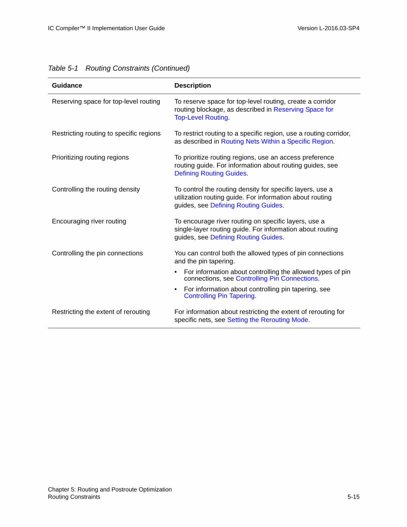
IC Compiler™ II Implementation User Guide Version L-2016.03-SP4
Reserving space for top-level routing To reserve space for top-level routing, create a corridor routing blockage, as described in Reserving Space for Top-Level Routing.
Restricting routing to specific regions To restrict routing to a specific region, use a routing corridor, as described in Routing Nets Within a Specific Region.
Prioritizing routing regions To prioritize routing regions, use an access preference routing guide. For information about routing guides, see Defining Routing Guides.
Controlling the routing density To control the routing density for specific layers, use a utilization routing guide. For information about routing guides, see Defining Routing Guides.
Encouraging river routing To encourage river routing on specific layers, use a single-layer routing guide. For information about routing guides, see Defining Routing Guides.
Controlling the pin connections You can control both the allowed types of pin connections and the pin tapering.
• For information about controlling the allowed types of pin connections, see Controlling Pin Connections.
• For information about controlling pin tapering, see Controlling Pin Tapering.
Restricting the extent of rerouting For information about restricting the extent of rerouting for specific nets, see Setting the Rerouting Mode.
Table 5-1 Routing Constraints (Continued)
Guidance Description
Chapter 5: Routing and Postroute OptimizationRouting Constraints 5-15Chapter 5: Routing and Postroute OptimizationRouting Constraints 5-15

IC Compiler™ II Implementation User Guide L-2016.03-SP4IC Compiler™ II Implementation User Guide Version L-2016.03-SP4
Defining Routing Blockages
A routing blockage defines a region where routing is not allowed on specific layers. Zroute considers routing blockages to be hard constraints.
To define a routing blockage, use the create_routing_blockage command. At a minimum, you must define the boundary of the routing blockage and the affected layers.
• To create a rectangular routing blockage, use the -boundary option to specify the lower-left and upper-right corners of the rectangle using the following syntax: { {llx lly} {urx ury} }.
• To create a rectilinear routing blockage, use the -boundary option to specify the coordinates of the polygon using the following syntax: { {x1 y1} {x2 y2} ... }.
You can also create a rectilinear routing blockage by specifying the polygon as the combined area of a heterogeneous collection of objects with physical geometry, such as poly_rects, geo_masks, shapes, layers, and other physical objects. If you specify a layer, the resulting area includes the area of every shape on the layer. For all other objects, the resulting area includes the area of each object. If you use this method, the resulting area must resolve to a single, connected polygon; otherwise, the command fails.
• To specify the affected layers, use the -layers option.
Specify the routing layers by using the layer names from the technology file. The layers can be metal, via, or poly layers.
By default, the tool creates a routing blockage named RB_objId in the current block that prevents routing of all nets within the routing blockage boundary. The router must meet the minimum spacing requirements between the routing blockage boundary and the net shapes. Use the following options to change the default behavior:
• -name blockage_name
Specifies a name for the routing blockage.
• -cell cell
Creates the routing blockage in a different physical cell.
When you use this option, the tool creates the routing blockage in the cell's reference block using the coordinate system of the cell's top-level block.
• -zero_spacing
Disables the minimum spacing rule between the routing blockage boundary and the net shapes (zero minimum spacing).
When you use this option, the net shapes can touch, but not overlap, the routing blockage boundary.
Chapter 5: Routing and Postroute OptimizationRouting Constraints 5-16

IC Compiler™ II Implementation User Guide Version L-2016.03-SP4
Note: When you create a routing blockage to prevent via insertion, you must use the -zero_spacing option; otherwise, frame view extraction does not use the route guide to trim the via region.
• -nets nets
Applies the routing blockage only to the specified nets.
• -net_types list_of_types
Applies the routing blockage only to the specified net types.
Specify one or more of the following net types: analog_ground, analog_power, analog_signal, clock, deep_nwell, deep_pwell, ground, nwell, power, pwell, reset, scan, signal, tie_high, and tie_low. To remove the net type settings and prevent routing of all nets in the routing blockage, use the -net_types unset setting.
Note: The -nets and -net_types options are mutually exclusive; you can specify only one.
To prevent signal routing on the M1 layer within the rectangle with its lower-left corner at (0, 0) and its upper-right corner at (100, 100), use the following command:
icc2_shell> create_routing_blockage \-boundary { {0.0 0.0} {100.0 100.0} } \-net_types signal -layers M1
To prevent vias on the V1 layer within the rectangle with its lower-left corner at (0, 0) and its upper-right corner at (100, 100), use the following command:
icc2_shell> create_routing_blockage \-boundary { {0.0 0.0} {100.0 100.0} } \-net_types signal -layers V1 -zero_spacing
To prevent PG routing on the M2 layer within the rectangle with its lower-left corner at (0, 0) and its upper-right corner at (100, 100), use the following command:
icc2_shell> create_routing_blockage \-boundary { {0.0 0.0} {100.0 100.0} } \-net_types {power ground} -layers M2
Reserving Space for Top-Level Routing
To reserve space for top-level routing, create a corridor routing blockage by using the -reserve_for_top_level_routing option when you create the routing blockage.
During block-level implementation, a corridor routing blockage acts as a regular blockage to prevent routing in the blockage area. During frame view extraction, the tool removes the corridor routing blockage to allow top-level routing in this area.
Chapter 5: Routing and Postroute OptimizationRouting Constraints 5-17Chapter 5: Routing and Postroute OptimizationRouting Constraints 5-17

IC Compiler™ II Implementation User Guide L-2016.03-SP4IC Compiler™ II Implementation User Guide Version L-2016.03-SP4
Querying Routing Blockages
To find routing blockages, use the get_routing_blockages command. For example, to get all the routing blockages in a block, use the following command:
icc2_shell> get_routing_blockages *
To find the routing blockages for specific nets, use the -of_objects option to specify the nets of interest. For example, to find the routing blockages for the n1 net, use the following command:
icc2_shell> get_routing_blockages -of_objects [get_nets n1]
To find the routing blockages in a specific location, use the get_objects_by_location -classes routing_blockage command.
Removing Routing Blockages
To remove routing blockages from the current block, use the remove_routing_blockages command.
• To remove specific routing blockages, specify the routing blockages, either as a list or collection, such as that returned by the get_routing_blockages command.
• To remove all routing corridors, specify the -all option.
Defining Routing Guides
Routing guides provides routing directives for specific areas of a block. You can use routing guides to
• Control the routing direction
• Limit the number of edges in the nonpreferred direction
• Control the routing density
• Prioritize routing regions
• Encourage river routing
To define a routing guide, use the create_routing_guide command. When you define a routing guide, you must specify its rectangular boundary, as well as information specific to the purpose of the routing guide.
Chapter 5: Routing and Postroute OptimizationRouting Constraints 5-18

IC Compiler™ II Implementation User Guide Version L-2016.03-SP4
Note: Routing guides defined by this command are honored by Zroute; however, they are not honored by the Advanced Route tool.
To specify the boundary, use the -boundary option to specify the lower-left and upper-right corners of the rectangle using the following syntax: { {llx lly} {urx ury} }. To identify the purpose of the routing guide, use the following options:
• -preferred_direction_only
This option forces the router to route all nets in the preferred direction within the routing guide boundary. For details, see Using Routing Guides to Control the Routing Direction.
• -switch_preferred_direction
This option switches the preferred routing direction within the routing guide boundary. For details, see Using Routing Guides to Control the Routing Direction.
• -max_patterns
This option limits the number of occurrences of a specific routing pattern within the routing guide boundary. For details, see Using Routing Guides to Limit Edges in the Nonpreferred Direction.
• -horizontal_track_utilization
This option controls the routing density for horizontal tracks within the routing guide boundary. For details, see Using Routing Guides to Control the Routing Density.
• -vertical_track_utilization
This option controls the routing density for vertical tracks within the routing guide boundary. For details, see Using Routing Guides to Control the Routing Density.
• -access_preference
This option prioritizes regions within the routing guide boundary for routing. For details, see Using Routing Guides to Prioritize Routing Regions.
• -river_routing
This option encourages river routing within the routing guide boundary. For details, see Using Routing Guides to Encourage River Routing.
Chapter 5: Routing and Postroute OptimizationRouting Constraints 5-19Chapter 5: Routing and Postroute OptimizationRouting Constraints 5-19

IC Compiler™ II Implementation User Guide L-2016.03-SP4IC Compiler™ II Implementation User Guide Version L-2016.03-SP4
By default, the tool creates a routing guide named RD#n in the current block, where n is a unique integer. Use the following options to change the default behavior:
• To specify a name for the routing guide, use the -name option.
• To specify the routing layers affected by the routing guide, use the -layers option.
The -layers option is required when you use the -switch_preferred_direction, -max_patterns, and -river_routing options. For all other types of routing guides, if you do not specify the -layers option, the routing guide applies to all layers.
Specify the routing layers by using the layer names from the technology file.
• To create the routing guide in a different physical cell, use the -cell option.
When you use this option, the tool creates the routing guide in the cell's reference block using the coordinate system of the cell's top-level block.
See Also
• Querying Routing Guides
• Removing Routing Guides
Using Routing Guides to Control the Routing Direction
You can use a routing guide to control the routing direction within the routing guide boundary, either by requiring routes to be in the preferred direction within the routing guide boundary or by switching the preferred direction within the routing guide boundary.
• To force the router to route all nets in the preferred direction within the routing guide boundary, use the -preferred_direction_only option with the create_routing_guide command.
You can use this type of routing guide to prevent wrong-way jog wires on specific layers.
By default, this routing guide applies to all layers within the routing guide boundary. To require preferred direction routing only for specific layers, use the -layers option to specify the affected layers.
For example, to force the router to use only the preferred direction on the M4 layer within the rectangle with its lower-left corner at (0, 0) and its upper-right corner at (100, 100), use the following command:
icc2_shell> create_routing_guide -boundary {{0.0 0.0} {100.0 100.0}} \-layers {M4} -preferred_direction_only
• To switch the preferred routing direction within the routing guide boundary, use the -switch_preferred_direction option with the create_routing_guide command.
You can use this type of routing guide to allow routing over macros, which might reduce congestion for a block that contains much detour routing.
Chapter 5: Routing and Postroute OptimizationRouting Constraints 5-20
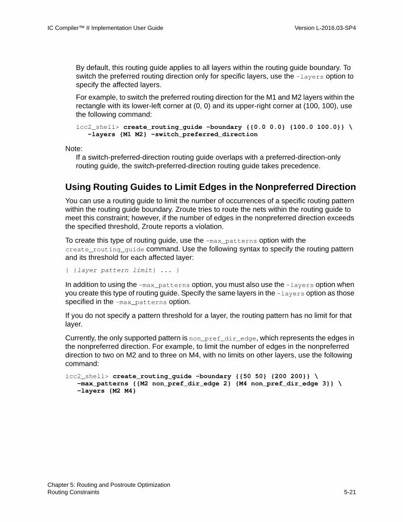
IC Compiler™ II Implementation User Guide Version L-2016.03-SP4
By default, this routing guide applies to all layers within the routing guide boundary. To switch the preferred routing direction only for specific layers, use the -layers option to specify the affected layers.
For example, to switch the preferred routing direction for the M1 and M2 layers within the rectangle with its lower-left corner at (0, 0) and its upper-right corner at (100, 100), use the following command:
icc2_shell> create_routing_guide -boundary {{0.0 0.0} {100.0 100.0}} \-layers {M1 M2} -switch_preferred_direction
Note: If a switch-preferred-direction routing guide overlaps with a preferred-direction-only routing guide, the switch-preferred-direction routing guide takes precedence.
Using Routing Guides to Limit Edges in the Nonpreferred Direction
You can use a routing guide to limit the number of occurrences of a specific routing pattern within the routing guide boundary. Zroute tries to route the nets within the routing guide to meet this constraint; however, if the number of edges in the nonpreferred direction exceeds the specified threshold, Zroute reports a violation.
To create this type of routing guide, use the -max_patterns option with the create_routing_guide command. Use the following syntax to specify the routing pattern and its threshold for each affected layer:
{ {layer pattern limit} ... }
In addition to using the -max_patterns option, you must also use the -layers option when you create this type of routing guide. Specify the same layers in the -layers option as those specified in the -max_patterns option.
If you do not specify a pattern threshold for a layer, the routing pattern has no limit for that layer.
Currently, the only supported pattern is non_pref_dir_edge, which represents the edges in the nonpreferred direction. For example, to limit the number of edges in the nonpreferred direction to two on M2 and to three on M4, with no limits on other layers, use the following command:
icc2_shell> create_routing_guide -boundary {{50 50} {200 200}} \-max_patterns {{M2 non_pref_dir_edge 2} {M4 non_pref_dir_edge 3}} \-layers {M2 M4}
Chapter 5: Routing and Postroute OptimizationRouting Constraints 5-21Chapter 5: Routing and Postroute OptimizationRouting Constraints 5-21

IC Compiler™ II Implementation User Guide L-2016.03-SP4IC Compiler™ II Implementation User Guide Version L-2016.03-SP4
Using Routing Guides to Control the Routing Density
You can use a routing guide to control the routing density within the routing guide boundary.
• To set the maximum track utilization for layers with a horizontal preferred direction, use the -horizontal_track_utilization option with the create_routing_guide command.
• To set the maximum track utilization for layers with a vertical preferred direction, use the -vertical_track_utilization option with the create_routing_guide command.
By default, when you create these routing guides, they apply to all layers within the routing guide boundary. To set the routing density only for specific layers, use the -layers option to specify the affected layers.
For example, to set a maximum track utilization of 50 percent for all layers with a horizontal preferred direction and a maximum track utilization of 30 percent for all layers with a vertical preferred direction within the rectangle with its lower-left corner at (0, 0) and its upper-right corner at (100, 100), use the following command:
icc2_shell> create_routing_guide -boundary {{0.0 0.0} {100.0 100.0}} \-horizontal_track_utilization 50 -vertical_track_utilization 30
Using Routing Guides to Prioritize Routing Regions
You can use a routing guide to prioritize regions within the routing guide boundary for routing. The regions are called access preference areas. You prioritize the access preference areas by assigning strengths to them. Access preference areas with higher strengths are preferred for routing. You can define access preference areas for both wires and vias. When you define a via access-preference area, you are defining a preference area for the via surrounds on the specified metal layer for vias coming from both above and below that metal layer.
To create this type of routing guide, use the -access_preference option with the create_routing_guide command. Use the following syntax to specify the access preference areas and their strengths:
{layer [{wire_access_preference wire_rect wire_strength}][{via_access_preference via_rect via_strength}] ...}
You can define multiple access preference areas. To define the relative preference of the access preference areas, use strength values between 0 and 1. If access preference areas overlap, the stronger access preference area takes precedence over the weaker access preference area. To require routing in a specific access preference area, use a strength value of 1. When you define access preference areas with a strength of 1, all access preference areas with a strength less than 1 are ignored and Zroute treats the access preference routing guide as a hard constraint.
Chapter 5: Routing and Postroute OptimizationRouting Constraints 5-22

IC Compiler™ II Implementation User Guide Version L-2016.03-SP4
The following example creates an access preference routing guide whose boundary is a rectangle with its lower-left corner at (0, 0) and its upper-right corner at (300, 300). It contains one wire access-preference area with coordinates of (0, 0) and (2, 1) and two via access-preference areas, one with coordinates of (0, 0) and (5, 5) and one with coordinates of (40, 40) and (45, 45). The wire access-preference area is slightly preferred over areas outside of the access preference area because it has a strength of 0.2. The via access-preference area with coordinates at (40, 40) and (45, 45) is ignored, because routing is required in the via access-preference area with coordinates at (0, 0) and (5, 5), which has a strength of 1.
icc2_shell> create_routing_guide -boundary {{0 0} {300 300}} \-access_preference {M1 {wire_access_preference {{0 0} {2 1}} 0.2}
{via_access_preference {{0 0} {5 5}} 1.0} {via_access_preference {{40 40} {45 45}} 0.5}}
To report information about the access preference routing guides defined for your block, use the report_routing_guides command.
Using Routing Guides to Encourage River Routing
River routing is a special routing topology that tries to minimize the space taken by the router by compressing the routes to follow a particular contour. River routing is useful if there are tight routing channels or you need to minimize the space taken by routing. You can use a routing guide to encourage river routing within the routing guide boundary.
To create this type of routing guide, use the -river_routing option with the create_routing_guide command. You must also use the -layers option to specify the affected layers.
For example, to encourage river routing on the M2 layer within the rectangle with its lower-left corner at (0, 0) and its upper-right corner at (100, 100), use the following command:
icc2_shell> create_routing_guide -boundary {{0.0 0.0} {100.0 100.0}} \-river_routing -layers {M2}
Chapter 5: Routing and Postroute OptimizationRouting Constraints 5-23Chapter 5: Routing and Postroute OptimizationRouting Constraints 5-23

IC Compiler™ II Implementation User Guide L-2016.03-SP4IC Compiler™ II Implementation User Guide Version L-2016.03-SP4
Querying Routing Guides
To find routing guides, use the get_routing_guides command. For example, to get all the routing guides in your block, use the following command:
icc2_shell> get_routing_guides *
To find the routing guides in a specific location, use the get_objects_by_location -classes routing_guide command.
Removing Routing Guides
To remove routing guides from the current block, use the remove_routing_guides command.
• To remove specific routing guides, specify the routing rules, either as a list or collection, such as that returned by the get_routing_guides command.
• To remove all routing guides, specify the -all option.
For example, to remove the new_width_rule routing rule, use the following command:
icc2_shell> remove_routing_rules new_width_rule
Routing Nets Within a Specific Region
To route one or more nets within a specific region,
1. Define a routing corridor by using the create_routing_corridor command, as described in Defining Routing Corridors.
2. Assign the nets to the routing corridor by using the add_to_routing_corridor command, as described in Assigning Nets to a Routing Corridor.
3. Verify that the routing corridors are valid by using the check_routing_corridors command, as described in Verifying Routing Corridors.
If necessary, modify the routing corridors, as described in Modifying Routing Corridors.
4. Route the nets by using the route_group command, as described in Routing Critical Nets.
5. Remove the routing corridors, as described in Removing Routing Corridors.
See Also
• Reporting Routing Corridors
Chapter 5: Routing and Postroute OptimizationRouting Constraints 5-24

IC Compiler™ II Implementation User Guide Version L-2016.03-SP4
Defining Routing Corridors
A routing corridor restricts Zroute global routing for specific nets to the region defined by a set of connected rectangles. In addition to specifying the region in which the routing occurs, you can also specify the minimum and maximum routing layers for each of the rectangles that comprise the routing corridor.
Routing corridors are intended to be used to route critical nets before signal routing. Zroute global routing considers routing corridors as a hard constraint, while track assignment and detail routing consider routing corridors as a soft constraint and might route nets slightly outside of the routing corridor to fix DRC violations.
Note: If a routing guide overlaps with a routing corridor and its attributes conflict with the routing corridor, the routing corridor takes precedence.
For example, Figure 5-2 shows a routing corridor named corridor_1, which is made up of six rectangles. This routing corridor is associated with the nets shown in yellow. The figure on the left shows the nets before routing, while the figure on the right shows the nets routed within the routing corridor.
Figure 5-2 Using a Routing Corridor
To define a routing corridor, use the create_routing_corridor command. At a minimum, you must define the boundary of the routing corridor.
• To create a rectangular routing corridor, use the -boundary option to specify the lower-left and upper-right corners of the rectangle using the following syntax: { {llx lly} {urx ury} }.
• To create a rectilinear routing corridor, use the -boundary option to specify the coordinates of the polygon using the following syntax: { {x1 y1} {x2 y2} ... }.
Before routing After routing
Chapter 5: Routing and Postroute OptimizationRouting Constraints 5-25Chapter 5: Routing and Postroute OptimizationRouting Constraints 5-25

IC Compiler™ II Implementation User Guide L-2016.03-SP4IC Compiler™ II Implementation User Guide Version L-2016.03-SP4
• To create a path-based routing corridor, use the -path option to specify the path and the -width option to specify the width in microns. Specify the path using the following syntax: { {x1 y1} {x2 y2} ... }.
By default, path-based routing corridors have flush end caps at the start and end of the path. To change the end cap style, use the -start_endcap and -end_endcap options. Valid styles are flush, full_width, and half_width.
By default, the tool creates a routing corridor named CORRIDOR_objId in the current block that honors the existing minimum and maximum routing layer constraints (for information about specifying routing layer constraints, see Specifying the Routing Resources). Use the following options to change the default behavior.
• To specify a name for the routing corridor, use the -name option.
• To create the routing guide in a different physical cell, use the -cell option.
When you use this option, the tool creates the routing guide in the cell's reference block using the coordinate system of the cell's top-level block.
• To specify the minimum and maximum routing layers for the routing corridor, use the -min_layer_name and -max_layer_name options.
Specify the routing layers by using the layer names from the technology file.
Assigning Nets to a Routing Corridor
To assign nets to a routing corridor, use the add_to_routing_corridor command. You must specify the routing corridor and the nets to add to it. You can assign a net to only one routing corridor and that routing corridor must cover all pins connected to the associated nets.
For example, to define a routing corridor named corridor_a and assign the nets named n1 and n2 to this routing corridor, use the following commands:
icc2_shell> create_routing_corridor -name corridor_a \-boundary { {10 10} {20 35} } \-min_layer_name M2 -max_layer_name M4
icc2_shell> create_routing_corridor_shape -routing_corridor corridor_a \-boundary { {20 25} {40 35} } \-min_layer_name M2 -max_layer_name M4
icc2_shell> create_routing_corridor_shape -routing_corridor corridor_a \-boundary { {40 10} {50 35} } \-min_layer_name M2 -max_layer_name M4
icc2_shell> add_to_routing_corridor corridor_a [get_nets {n1 n2}]
Note: You can also assign nets to the routing corridor by using the -object option when you use the create_routing_corridor command to create the routing corridor.
Chapter 5: Routing and Postroute OptimizationRouting Constraints 5-26

IC Compiler™ II Implementation User Guide Version L-2016.03-SP4
Verifying Routing Corridors
To successfully route a net within a routing corridor, the routing corridor must meet the following requirements:
• It must be a contiguous region; all regions that comprise the routing corridor must be connected.
• It must contain the pins that connect to the nets associated with the routing corridor.
To verify that a routing corridor meets these requirements, use the check_routing_corridors command.
icc2_shell> check_routing_corridors RC_0
You can view the errors detected by the check_routing_corridors command in the message browser.
Modifying Routing Corridors
You can make the following modifications to an existing routing corridor:
• Add new shapes to the routing corridor.
To add new shapes, use the create_routing_corridor_shape command. Use the -routing_corridor option to specify the routing corridor that you want to update. You must specify the boundary of the routing corridor by using the -boundary or -path option (for details about these options, see Defining Routing Corridors). You can also specify the minimum and maximum routing layers for the shape by using the -min_layer_name and -max_layer_name options.
• Remove rectangles from the routing corridor.
To remove shapes, use the remove_routing_corridor_shapes command.
• Change the nets associated with the routing corridor.
To add nets to a routing corridor, use the add_to_routing_corridor command. To remove nets from a routing corridor, use the remove_from_routing_corridor command.
You can also modify routing corridors in the GUI by using the Create Route Corridor tool, the Move/Resize tool, or the Delete tool, or by editing the attributes in the Properties dialog box.
Reporting Routing Corridors
To report the routing corridors in your block, use the report_routing_corridors command. By default, the command reports all routing corridors; to report specific routing corridors, specify the routing corridors to report.
Chapter 5: Routing and Postroute OptimizationRouting Constraints 5-27Chapter 5: Routing and Postroute OptimizationRouting Constraints 5-27

IC Compiler™ II Implementation User Guide L-2016.03-SP4IC Compiler™ II Implementation User Guide Version L-2016.03-SP4
By default, the command reports the following information for each routing corridor: its name; the shapes associated with the routing corridor, including their names, minimum routing layer, maximum routing layer, and boundary; the connectivity of the routing corridor shapes; and the nets associated with the routing corridor. To output a Tcl script that re-creates the routing corridors, use the -output option.
To report the routing corridor for a specific net, use the get_routing_corridors command. When you run this command, you must use the -of_objects option to specify the nets of interest.
Removing Routing Corridors
To remove routing corridors from the current block, use the remove_routing_corridors command.
• To remove specific routing corridors, specify the routing corridors, either as a list or collection, such as that returned by the get_routing_corridors command.
• To remove all routing corridors, specify the -all option.
You can also remove routing corridors in the GUI by using the Delete tool.
Using Nondefault Routing Rules
Zroute supports the use of nondefault routing rules, both for routing and for shielding.
• For routing, you can use nondefault routing rules to define stricter wire width and spacing rules, to define the pin tapering distance, to specify the vias used when routing nets with nondefault routing rules, and to specify multiple-patterning mask constraints.
• For shielding, you can use nondefault routing rules to define the minimum width and spacing rules.
For information about working with nondefault routing rules, see the following topics:
• Defining Nondefault Routing Rules
• Reporting Nondefault Routing Rule Definitions
• Removing Nondefault Routing Rules
• Modifying Nondefault Routing Rules
• Assigning Nondefault Routing Rules to Nets
• Reporting Nondefault Routing Rule Assignments
Chapter 5: Routing and Postroute OptimizationRouting Constraints 5-28

IC Compiler™ II Implementation User Guide Version L-2016.03-SP4
Defining Nondefault Routing Rules
To define a nondefault routing rule, use the create_routing_rule command. When you define a nondefault routing rule, you must specify a name for the nondefault routing rule. You use the name to assign the nondefault routing rule to nets or clocks.
The following topics describe how to create nondefault routing rules for various purposes:
• Defining Minimum Wire Width Rules
• Defining Minimum Wire Spacing Rules
• Defining Minimum Via Spacing Rules
• Specifying Nondefault Vias
• Specifying Mask Constraints
• Defining Shielding Rules
You can create a single routing rule that serves multiple purposes. In addition, you can assign multiple nondefault routing rules to a net.
Defining Minimum Wire Width Rules
You can define nondefault minimum wire width rules that are stricter than the minimum width rules defined in the technology file. Nondefault minimum width rules are hard constraints, which must be met during routing.
Note: The minimum width defined in a nondefault routing rule applies to all metal segments, including via enclosures. To avoid DRC violations, ensure that the enclosures for nondefault vias meet the minimum width rule.
To define a minimum wire width rule, use the create_routing_rule command. You can specify the minimum width by specifying a multiplier that is applied to the default width for each layer, by specifying the minimum width in microns for each layer, or both.
• To use a multiplier to specify the minimum width, use the following syntax:
create_routing_rule rule_name[-default_reference_rule | -reference_rule_name ref_rule]-multiplier_width multiplier
The multiplier value must be between 0.001 and 2000. The default width for each layer is determined from the reference rule, which is either the default routing rule or the reference rule specified in the -reference_rule_name option.
Chapter 5: Routing and Postroute OptimizationRouting Constraints 5-29Chapter 5: Routing and Postroute OptimizationRouting Constraints 5-29

IC Compiler™ II Implementation User Guide L-2016.03-SP4IC Compiler™ II Implementation User Guide Version L-2016.03-SP4
For example, to define a nondefault routing rule named new_width_rule that uses the default routing rule as the reference rule and defines the nondefault width as two times the default width, use the following command:
icc2_shell> create_routing_rule new_width_rule -multiplier_width 2.0
• To specify the minimum width values for each layer, use the following syntax:
create_routing_rule rule_name[-default_reference_rule | -reference_rule_name ref_rule]-widths {layer1 width1 layer2 width2 … layern widthn}
Specify the routing layers by using the layer names from the technology file. You can specify a single width value per layer. Zroute uses the wire width from the reference rule, which is either the default routing rule or the reference rule specified in the -reference_rule_name option, for any layers not specified in the -widths option.
For example, to define a nondefault routing rule named new_width_rule2 that uses the default routing rule as the reference rule and defines nondefault width rules for the M1 and M4 layers, use the following command:
icc2_shell> create_routing_rule new_width_rule2 \-widths {M1 0.8 M4 0.9}
• If you specify both with -multiplier_width option and the -widths option, the tool uses the -widths option to determine the base width, and then applies the multiplier to that value to determine the minimum width requirement.
For example, to define a nondefault routing rule named new_width_rule3 that uses the default routing rule as the reference rule and defines the nondefault width as 0.8 for the M1 layer, 0.9 for the M4 layer, and two times the default width for all other layers, use the following command:
icc2_shell> create_routing_rule new_width_rule3 \-multiplier_width 2.0 -widths {M1 0.4 M4 0.45}
Defining Minimum Wire Spacing Rules
You can define nondefault minimum wire spacing rules that are stricter than the rules defined in the technology file. Nondefault wire spacing rules can be defined as hard constraints, which must be met, or as soft constraints, which Zroute tries to meet.
Note: The spacing rules defined in the technology file are always considered hard constraints.
By default, Zroute checks the nondefault spacing rules between signal nets and other signal nets, PG nets, and blockages, but not between shapes of the same signal net or between
Chapter 5: Routing and Postroute OptimizationRouting Constraints 5-30

IC Compiler™ II Implementation User Guide Version L-2016.03-SP4
signal nets and shield wires for PG nets. For information about modifying these checks, see Configuring Nondefault Spacing Checks.
To define a minimum wire spacing rule, use the create_routing_rule command. You can specify the minimum spacing by specifying a multiplier that is applied to the default spacing for each layer, by specifying the minimum spacings in microns for each layer, or both.
• To use a multiplier to specify the minimum spacing, use the following syntax:
create_routing_rule rule_name[-default_reference_rule | -reference_rule_name ref_rule]-multiplier_spacing multiplier
The multiplier value must be between 0.001 and 2000. The default wire spacing for each layer is determined from the reference rule, which is either the default routing rule or the reference rule specified in the -reference_rule_name option.
For example, to define a nondefault routing rule named new_spacing_rule that uses the default routing rule as the reference rule and defines the nondefault spacing as two times the default spacing, use the following command:
icc2_shell> create_routing_rule new_spacing_rule \-multiplier_spacing 2.0
• To specify the minimum spacing values for each layer, use the following syntax:
create_routing_rule rule_name-spacings { layer1 {spacing11 spacing12 ... spacing1n}
layer2 {spacing21 spacing22 ... spacing2n}... layern {spacingn1 spacingn2 ...spacingnn} }
-spacing_weight_levels { layer1 {weight11 weight12 ... weight1n}layer2 {weight21 weight22 ... weight2n}... layern {weightn1 weightn2 ... weightnn} }
Specify the routing layers by using the layer names from the technology file. You can define multiple spacing values per layer. Zroute uses the spacing values from the reference rule, which is either the default routing rule or the reference rule specified in the -reference_rule_name option, for any layers not specified in the -spacings option.
If you specify more than one spacing value per layer, you must assign a weight to each spacing value by using the -spacing_weight_levels option. The valid weight values are low, medium, high, and hard. When you assign a weight level other than hard, the spacing rule is a soft spacing rule. By default, Zroute does not fix soft routing rule violations. To fix soft routing rules, you must map the weight levels to routing effort levels, as described in Specifying the Routing Effort for Soft Spacing Violations.
Chapter 5: Routing and Postroute OptimizationRouting Constraints 5-31Chapter 5: Routing and Postroute OptimizationRouting Constraints 5-31

IC Compiler™ II Implementation User Guide L-2016.03-SP4IC Compiler™ II Implementation User Guide Version L-2016.03-SP4
For example, to define a nondefault routing rule named new_spacing_rule2 that uses the default routing rule as the reference rule and defines nondefault spacing rules for the M1 and M4 layers, use the following command:
icc2_shell> create_routing_rule new_spacing_rule2 \-spacings { M1 {0.12 0.24} M4 {0.14 0.28} } \-spacing_weight_levels { M1 {hard medium} M4 {hard medium} }
• If you specify both with -multiplier_spacing option and the -spacings option, the tool uses the -spacings option to determine the base spacing, and then applies the multiplier to that value to determine the minimum wire spacing requirement.
Configuring Nondefault Spacing Checks
You can configure the checking of nondefault spacing rules by enabling or disabling checks between signal nets and other objects. In addition, you can ignore violations of the nondefault spacing rules for short parallel distances.
• To honor nondefault spacing rules between shapes of the same signal net, set the route.detail.var_spacing_to_same_net application option to true.
• To honor nondefault spacing rules between signal nets and shield wires for PG nets
❍ For all signal nets, set the route.common.ignore_var_spacing_to_shield application option to false
❍ For specific signal nets, use the -ignore_spacing_to_shield false option when you define the nondefault spacing rule with the create_routing_rule command
• To ignore nondefault spacing rules between signal nets and PG nets
❍ For all signal nets, set the route.common.ignore_var_spacing_to_pg application option to true
❍ For specific signal nets, use the -ignore_spacing_to_pg true option when you define the nondefault spacing rule with the create_routing_rule command
Note: When you ignore nondefault spacing rules between signal nets and PG nets, the rules are also ignored between the signal nets and the shield wires regardless of the setting of the route.common.ignore_var_spacing_to_shield and create_routing_rule -ignore_spacing_to_shield options.
• To ignore nondefault spacing rules between signal nets and blockages
❍ For all signal nets, set the route.common.ignore_var_spacing_to_blockage application option to true
❍ For specific signal nets, use the -ignore_spacing_to_blockage true option when you define the nondefault spacing rule with the create_routing_rule command
Chapter 5: Routing and Postroute OptimizationRouting Constraints 5-32

IC Compiler™ II Implementation User Guide Version L-2016.03-SP4
You can relax the nondefault spacing checks for specific nondefault routing rules by ignoring violations for short parallel distances, as shown in Figure 5-3. This technique increases the flexibility of DRC convergence without adversely affecting crosstalk.
Figure 5-3 Ignoring Nondefault Spacing Rule Violations
To define the length thresholds within which to ignore the nondefault spacing violations, use the -spacing_length_thresholds option when you creating the nondefault routing rule with the create_routing_rule command. The length threshold values are in microns and must have a one-to-one correspondence with the spacing entries specified in the -spacings option.
For example,
icc2_shell> create_routing_rule new_rule \-spacings { M1 {0.09 0.15 0.2}
M2 {0.09 0.15 0.2} M3 {0.09 0.15 0.2} } \
-spacing_weight_levels { M1 {hard medium low} M2 {hard medium low} M3 {hard medium low} } \
-spacing_length_thresholds { M1 {0.01 0 0} M2 {0.01 0 0} M3 {0.01 0 0} }
Chapter 5: Routing and Postroute OptimizationRouting Constraints 5-33Chapter 5: Routing and Postroute OptimizationRouting Constraints 5-33

IC Compiler™ II Implementation User Guide L-2016.03-SP4IC Compiler™ II Implementation User Guide Version L-2016.03-SP4
Specifying the Routing Effort for Soft Spacing Violations
By default, Zroute does not fix soft spacing violations. To fix soft spacing violations, you must assign a routing effort to each of the soft weight levels. These assignments apply to all soft spacing rules.
To assign a routing effort for each weight level, use the following syntax to set the route.common.soft_rule_weight_to_effort_level_map application option:
set_app_options -name route.common.soft_rule_weight_to_effort_level_map-value { {weight effort} ... }
Each weight argument can be one of low, medium, or high. You should specify each weight level only one time; if you specify a weight level multiple times, the router uses the last specification. Each effort argument can be one of the following values:
• off (the default)
Zroute does not fix the soft spacing rule violations.
• low
Zroute uses a small number of rip-up and reroute passes to resolve soft spacing rule violations.
• medium
Zroute uses a medium number of rip-up and reroute passes to resolve soft spacing rule violations. Note that you cannot specify this effort level for the low weight level.
• high
Zroute treats soft spacing rule violations the same as regular design rule violations during rip up and reroute. Note that you cannot specify this effort level for the low weight level.
For example, to assign low routing effort to low-weight soft spacing rules, medium routing effort to medium-weight soft spacing rules, and high routing effort to high-weight soft spacing, use the following command:
icc2_shell> set_app_options \-name route.common.soft_rule_weight_to_effort_level_map \-value { {low low} {medium medium} {high high} }
Chapter 5: Routing and Postroute OptimizationRouting Constraints 5-34

IC Compiler™ II Implementation User Guide Version L-2016.03-SP4
Defining Minimum Via Spacing Rules
You can define nondefault minimum via spacing rules that are stricter than the rules defined in the technology file. Nondefault via spacing rules are hard constraints that must be met.
To define a minimum via spacing rule, use the -via_spacings option with the create_routing_rule command using the following syntax:
create_routing_rule rule_name-via_spacings { {layer1 layer2 spacing} ... }
Specify the routing layers by using the layer names from the technology file. You can define a single width value per layer pair.
The minimum via spacing for vias between any unspecified layer combinations is determined from the technology file. For vias on the same layer, the router uses the minimum spacing defined in the Layer section for the via layer. For vias on different layers, the router uses the minimum spacing defined in the DesignRule section for the via layer combination.
For example, to define a nondefault routing rule named via_spacing_rule that defines nondefault spacing rules between vias on the V1 layer and between vias on the V1 and V2 layers, and uses the minimum spacing rules defined in the technology file between vias on all other layer combinations, use the following command:
icc2_shell> create_routing_rule via_spacing_rule \-via_spacings {{V1 V1 2.3} {V1 V2 3.2}}
Specifying Nondefault Vias
By default, when routing nets with nondefault routing rules, Zroute selects vias from the technology file based on the design rules.
To specify the vias to use when routing nets with nondefault routing rules, use the create_routing_rule command. You can define the nondefault vias by using either the -cuts option or the -vias option.
• When you use the -cuts option, the tool determines the suitable via definitions from the technology file based on the specification in the -cuts option and the rules defined in the technology file.
• When you use the -vias option, you explicitly specify the nondefault via definitions, including the allowed cut numbers and rotation for each via definition.
Chapter 5: Routing and Postroute OptimizationRouting Constraints 5-35Chapter 5: Routing and Postroute OptimizationRouting Constraints 5-35
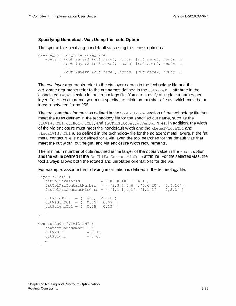
IC Compiler™ II Implementation User Guide L-2016.03-SP4IC Compiler™ II Implementation User Guide Version L-2016.03-SP4
Specifying Nondefault Vias Using the -cuts Option
The syntax for specifying nondefault vias using the -cuts option is
create_routing_rule rule_name-cuts { {cut_layer1 {cut_name1, ncuts} {cut_name2, ncuts} …}
{cut_layer2 {cut_name1, ncuts} {cut_name2, ncuts} …}...{cut_layern {cut_name1, ncuts} {cut_name2, ncuts} …}
}
The cut_layer arguments refer to the via layer names in the technology file and the cut_name arguments refer to the cut names defined in the cutNameTbl attribute in the associated Layer section in the technology file. You can specify multiple cut names per layer. For each cut name, you must specify the minimum number of cuts, which must be an integer between 1 and 255.
The tool searches for the vias defined in the ContactCode section of the technology file that meet the rules defined in the technology file for the specified cut name, such as the cutWidthTbl, cutHeightTbl, and fatTblFatContactNumber rules. In addition, the width of the via enclosure must meet the nondefault width and the xLegalWidthTbl and yLegalWidthTbl rules defined in the technology file for the adjacent metal layers. If the fat metal contact rule is not defined for a via layer, the tool searches for the default vias that meet the cut width, cut height, and via enclosure width requirements.
The minimum number of cuts required is the larger of the ncuts value in the -cuts option and the value defined in the fatTblFatContactMinCuts attribute. For the selected vias, the tool always allows both the rotated and unrotated orientations for the via.
For example, assume the following information is defined in the technology file:
Layer "VIA1" {fatTblThreshold = ( 0, 0.181, 0.411 )fatTblFatContactNumber = ( "2,3,4,5,6 ","5,6,20", "5,6,20" )fatTblFatContactMinCuts = ( "1,1,1,1,1", "1,1,1", "2,2,2" )
cutNameTbl = ( Vsq, Vrect )cutWidthTbl = ( 0.05, 0.05 )cutHeightTbl = ( 0.05, 0.13 )…
}
ContactCode "VIA12_LH" {contactCodeNumber = 5cutWidth = 0.13cutHeight = 0.05…
}
Chapter 5: Routing and Postroute OptimizationRouting Constraints 5-36

IC Compiler™ II Implementation User Guide Version L-2016.03-SP4
ContactCode "VIA12_LV" {contactCodeNumber = 6cutWidth = 0.05cutHeight = 0.13…
}ContactCode "VIA12_P" {
contactCodeNumber = 20cutWidth = 0.05cutHeight = 0.05…
}
If you use the following command,
icc2_shell> create_routing_rule cut_rule -cuts {VIA1 {Vrect 1}}
The tool selects the following vias: {VIA12_LH 1x1 R}, {VIA12_LH 1x1 NR}, {VIA12_LV 1x1 R}, {VIA12_LV 1x1 NR}, {VIA12_LH 1x2 R}, {VIA12_LH 1x2 NR}, {VIA12_LH 2x1 R}, {VIA12_LH 2x1 NR}, {VIA12_LV 1x2 R}, {VIA12_LV 1x2 NR}, {VIA12_LV 2x1 R}, and {VIA12_LV 2x1 NR}.
Specifying Nondefault Vias Using the -vias Option
The syntax for specifying nondefault vias using the -vias option is
create_routing_rule rule_name-vias { {via_type1 cut_number1 orientation1}
{via_type2 cut_number2 orientation2}...{via_typen cut_numbern orientationn}
}
You can specify multiple via types per layer; each via type must be a via definition defined in the technology file or a via definition created by the create_via_def command. For each via type, you must explicitly specify the allowed cut numbers and orientation. To specify the orientation, use NR to indicate that the via is not rotated or R to indicate that the via is rotated. The order of via specification is not important; during routing, Zroute selects the lowest cost nondefault via.
For example, to specify the vias selected by the -cuts option in the previous example, use the following command:
icc2_shell> create_routing_rule via_rule \-vias { {VIA12_LH 1x1 R} {VIA12_LH 1x1 NR} {VIA12_LV 1x1 R}
{VIA12_LV 1x1 NR} {VIA12_LH 1x2 R} {VIA12_LH 1x2 NR}{VIA12_LH 2x1 R} {VIA12_LH 2x1 NR} {VIA12_LV 1x2 R} {VIA12_LV 1x2 NR} {VIA12_LV 2x1 R} {VIA12_LV 2x1 NR} }
Chapter 5: Routing and Postroute OptimizationRouting Constraints 5-37Chapter 5: Routing and Postroute OptimizationRouting Constraints 5-37

IC Compiler™ II Implementation User Guide L-2016.03-SP4IC Compiler™ II Implementation User Guide Version L-2016.03-SP4
Specifying Mask Constraints
If you are using the precolored design flow for a design that uses multiple-patterning technology, you can set mask constraints on timing-critical nets, such as clock nets, by defining a precoloring rule and applying it to the nets. For details about the mask constraints, see Mask Constraints.
To define a precoloring rule, use the create_routing_rule command using the following syntax:
create_routing_rule rule_name -mask_constraints {layer1 constraint1 layer2 constraint2 ... layern constraintn}
where constraint is one of same_mask, mask1_soft, or mask2_soft.
For example, to define a precoloring routing rule that sets mask_one constraints on the M4 and M5 layers, use the following command:
icc2_shell> create_routing_rule clock_mask1 \-mask_constraints {M4 mask_one M5 mask_one}
Note: To ensure DRC convergence, you should set double-patterning mask constraints only on a very few timing-critical nets.
Defining Shielding Rules
To define shielding rules, use the create_routing_rule command using the following syntax:
create_routing_rule rule_name-shield_widths {layer1 width1 layer2 width2 … layern widthn}-shield_spacings {layer1 spacing1 layer2 spacing2 … layern spacingn}[-snap_to_track]
Specify the routing layers by using the layer names from the technology file. You can define a single width and spacing value per layer. Zroute uses the default wire width for any layers not specified in the -shield_widths option and the default spacing for any layers not specified in the -shield_spacings option.
By default, shielding wires are not snapped to the routing tracks. To snap shielding wires to the routing tracks, use the -snap_to_track option when you define the nondefault routing rule.
Chapter 5: Routing and Postroute OptimizationRouting Constraints 5-38

IC Compiler™ II Implementation User Guide Version L-2016.03-SP4
For example, to specify a shielding rule that uses spacing of 0.1 microns and a width of 0.1 microns for M1 through M5 and spacing of 0.3 microns and a width of 0.3 microns for M6, use the following command:
icc2_shell> create_routing_rule shield_rule \-shield_widths {M1 0.1 M2 0.1 M3 0.1 M4 0.1 M5 0.1 M6 0.3} \-shield_spacings {M1 0.1 M2 0.1 M3 0.1 M4 0.1 M5 0.1 M6 0.3}
Reporting Nondefault Routing Rule Definitions
To report the nondefault routing rules defined by the create_routing_rule command, use the report_routing_rules -verbose command. By default, this command reports all of the nondefault routing rules for the current block. To limit the report to specific nondefault routing rules, specify the rule names as an argument to the command.
icc2_shell> report_routing_rules {rule_names}
To output a Tcl script that contains the create_routing_rule commands used to define the specified nondefault routing rules, use the -output option when you run the report_routing_rules command.
Removing Nondefault Routing Rules
To remove nondefault routing rules from the current block, use the remove_routing_rules command. When you remove a nondefault routing rule, the rule is removed from all nets to which it is applied and the rule definition is removed from the design library.
• To remove specific routing rules, specify the routing rules.
• To remove all routing rules, specify the -all option.
For example, to remove the new_width_rule routing rule, use the following command:
icc2_shell> remove_routing_rules new_width_rule
Modifying Nondefault Routing Rules
To change the definition for an existing rule, you must use the remove_routing_rules command to remove the rule and then use the create_routing_rule command to redefine the rule. The tool issues an error message if you try to redefine an existing routing rule.
Chapter 5: Routing and Postroute OptimizationRouting Constraints 5-39Chapter 5: Routing and Postroute OptimizationRouting Constraints 5-39

IC Compiler™ II Implementation User Guide L-2016.03-SP4IC Compiler™ II Implementation User Guide Version L-2016.03-SP4
Assigning Nondefault Routing Rules to Nets
The IC Compiler II tool provides two commands for assigning nondefault routing rules to nets:
• set_clock_routing_rules
This command assigns nondefault routing rules to clock nets before clock tree synthesis. During clock tree synthesis and optimization, the tool propagates the nondefault routing rules to the newly created clock nets.
• set_routing_rule
This command assigns nondefault routing rules to signal nets and to clock nets after clock tree synthesis.
The following topics describe how to assign nondefault routing rules to nets:
• Assigning Nondefault Routing Rules to Clock Nets
• Assigning Nondefault Routing Rules to Signal Nets
Assigning Nondefault Routing Rules to Clock Nets
To assign a clock routing rule to a clock net, use the -rule option with the set_clock_routing_rules command. The specified rule must be a rule that you previously defined with the create_routing_rule command.
To reset a clock routing rule to the default routing rule, use the -default_rule option. To change a clock routing rule, first reset it to the default routing rule and then use the -rule option after resetting the assignment to the default routing rule.
By default, the set_clock_routing_rules command assigns the specified clock routing rule to all clock trees in the block. Table 5-2 shows the options used to restrict the routing rule assignment.
Table 5-2 Restricting Clock Routing Rule Assignments
To assign a nondefault routing rule to Use this option
Specific clock trees -clocks clocks
Nets connected to the clock root1 -net_type root
Nets connected to one or more clock sinks1 -net_type sink
Chapter 5: Routing and Postroute OptimizationRouting Constraints 5-40

IC Compiler™ II Implementation User Guide Version L-2016.03-SP4
Figure 5-4 shows the root, sink, and internal nets of a clock tree after clock tree synthesis. Note that the root-net routing rule is applied to all the single-fanout clock nets starting from the clock root up to the point where the clock tree branches out to a fanout of more than one. Internal-net routing rules are applied to the nets from this point until the sink nets.
Figure 5-4 Root, Internal, and Sink Clock Net Types
For example, to assign a shielding rule called shield_rule to the nets in the CLK clock tree before clock tree synthesis, use the following command:
icc2_shell> set_clock_routing_rules -clocks CLK \-rules shield_rule
To assign different nondefault routing rules to each net type for all clock trees in the block, use the following commands:
icc2_shell> set_clock_routing_rules -rules NDR1 -net_type root icc2_shell> set_clock_routing_rules -rules NDR2 -net_type internal icc2_shell> set_clock_routing_rules -rules NDR3 -net_type sink
During clock tree synthesis and optimization, the tool also honors nondefault routing rules set by using the set_routing_rule command. However, the tool does not propagate these routing rules to any new clock nets it creates.
Internal nets in the a clock tree (all nets except the
root and sink nets)1-net_type internal
Specific clock nets -nets nets
1. You can use this option with the -clocks option to further restrict the assignment. This option is not valid with the -nets option.
Table 5-2 Restricting Clock Routing Rule Assignments (Continued)
To assign a nondefault routing rule to Use this option
Sink nets
Internal nets
Root nets
Chapter 5: Routing and Postroute OptimizationRouting Constraints 5-41Chapter 5: Routing and Postroute OptimizationRouting Constraints 5-41

IC Compiler™ II Implementation User Guide L-2016.03-SP4IC Compiler™ II Implementation User Guide Version L-2016.03-SP4
If a net is assigned more than one nondefault routing rule, the tool uses the following priority to determine the effective routing rule:
1. Nondefault routing rule set by the set_routing_rule command
2. Net-specific clock routing rule set by the set_clock_routing_rules -nets command
3. Clock-specific clock routing rule set by the set_clock_routing_rules -clocks command
4. Global clock routing rule set by the set_clock_routing_rules command
Assigning Nondefault Routing Rules to Signal Nets
To assign a nondefault routing rule to a net, use the -rule option with the set_routing_rule command. The specified rule must be a rule that you previously defined with the create_routing_rule command. You must specify the nets to which to assign the nondefault routing rule. You can assign multiple nondefault routing rules to a net.
To change the routing rule assignment for one or more nets,
• Use the -default_rule option to reset the nets to the default routing rule.
To assign different nondefault routing rules to the nets, use the -rule option after resetting the nets to the default routing rule.
• Use the -no_rule option to remove all routing rules from the nets and allow the tool to automatically assign a routing rule to them.
• Use the -clear option to remove all routing rules and net-specific layer constraints from the nets.
For example, to assign a nondefault routing rule called WideMetal to the CLK net, use the following command:
icc2_shell> set_routing_rule -rule WideMetal [get_nets CLK]
To reset the routing rule for the CLK net to the default routing rule, use the following command:
icc2_shell> set_routing_rule -default_rule [get_nets CLK]
Chapter 5: Routing and Postroute OptimizationRouting Constraints 5-42

IC Compiler™ II Implementation User Guide Version L-2016.03-SP4
Reporting Nondefault Routing Rule Assignments
The IC Compiler II tool provides commands to report the nondefault routing rules assigned by the set_routing_rule command and the clock routing rules assigned by the set_clock_routing_rules command.
• To report the nondefault routing rules assigned by the set_routing_rule command, use the -of_objects option with the report_routing_rules command.
icc2_shell> report_routing_rules -of_objects [get_nets *]
• To report the clock routing rule assignments, use the report_clock_routing_rules command. This command reports only the routing rules assigned by the set_clock_routing_rules command.
Controlling Off-Grid Routing
You can prevent off-grid routing of wires or vias by requiring them to be aligned to the wire track or discourage off-grid routing of vias by increasing the cost associated with off-grid routing.
Preventing Off-Grid Routing
By default, wires and vias need to be aligned to the wire track grid for a metal layer only if the onWireTrack or onGrid attribute is set to 1 in its Layer section in the technology file.
To override the technology file settings, set the following application options:
• route.common.wire_on_grid_by_layer_name
This option controls off-grid routing for metal layers.
• route.common.via_on_grid_by_layer_name
This option controls off-grid routing for via layers.
Use the following syntax to set these options:
{ {layer true|false} ... }
Specify the layers by using the layer names from the technology file. Specify true to forbid off-grid routing and false to allow off-grid routing.
If you use either of these options, the tool ignores all settings for the onWireTrack and onGrid attributes in the technology file and uses only the settings specified by these options. If you do not specify a layer in these options, off-grid routing is allowed on that layer, regardless of the setting in the technology file.
Chapter 5: Routing and Postroute OptimizationRouting Constraints 5-43Chapter 5: Routing and Postroute OptimizationRouting Constraints 5-43

IC Compiler™ II Implementation User Guide L-2016.03-SP4IC Compiler™ II Implementation User Guide Version L-2016.03-SP4
For example, to prevent off-grid routing for wires on the M2 and M3 metal layers and for vias on the V2 via layer, regardless of the settings in the technology file, use the following commands:
icc2_shell> set_app_options \-name route.common.wire_on_grid_by_layer_name \-value {{M2 true} {M3 true}}
icc2_shell> set_app_options \-name route.common.via_on_grid_by_layer_name \-value {{V2 true}}
Discouraging Off-Grid Routing for Vias
To discourage off-grid routing for vias, you can increase the cost of routing the via enclosure metal shapes off the wire track grid. To specify the extra cost multiplier for the metal layers on which the via enclosures are routed, set the route.common.extra_via_off_grid_cost_multiplier_by_layer_name application option.
Use the following syntax to set this option:
{ {layer multiplier} ... }
Specify the layers by using the layer names from the technology file. The cost multiplier must be a value between 0.0 and 20.0.
When you specify this option, the effective cost is the base cost times (1+multiplier). For example, assume that the technology file defines the VIA12 layer between the M1 and M2 metal layers and the VIA23 via layer between the M2 and M3 metal layers. To set the extra cost multiplier for the via enclosures on the M2 metal layer (and therefore the vias on the VIA12 and VIA23 via layers) to 0.5 (for an effective via cost of 1.5 times the base cost), use the following command:
icc2_shell> set_app_options \-name route.common.extra_via_off_grid_cost_multiplier_by_layer_name \-value {{M2 0.5}}
Chapter 5: Routing and Postroute OptimizationRouting Constraints 5-44

IC Compiler™ II Implementation User Guide Version L-2016.03-SP4
Controlling Pin Connections
By default, Zroute connects a signal route to a pin by using wires or vias anywhere on the pin. To restrict the allowed types of pin connections on a per-layer basis, use the following syntax to set the route.common.connect_within_pins_by_layer_name application option:
set_app_options -name route.common.connect_within_pins_by_layer_name-value { {layer mode} ... }
Valid values for the mode argument are
• off (the default)
There are no restrictions on pin connections.
• via_standard_cell_pins
Only the connections to standard cell pins by using a via are restricted. When using a via connection, the via’s metal enclosure must be contained within the pin shape.
There are no restrictions on signal routes connected to macro cell and pad cell pins by using a via or to any pins by using wires.
• via_wire_standard_cell_pins
The connections to standard cell pins by using a via or a wire are restricted. When using a via connection, the via’s metal enclosure must be contained within the pin shape. When using a wire, the wire must be contained within the pin shape.
• via_all_pins
The connections to any pins (standard cell, macro cell, or pad cell) by using a via are restricted. When using a via connection, the via’s metal enclosure must be contained within the pin shape.
There are no restrictions on signal routes connected to any pins by using wires.
• via_wire_all_pins
The connections to any pins by using a via or a wire are restricted. When using a via connection, the via’s metal enclosure must be contained within the pin shape. When using a wire, the wire must be contained within the pin shape.
For example, if you use the following command (or use the default settings), all of the connections shown in Figure 5-5 are valid and no DRC violations are reported:
icc2_shell> set_app_options \-name route.common.connect_within_pins_by_layer_name \-value {{M1 off}}
Chapter 5: Routing and Postroute OptimizationRouting Constraints 5-45Chapter 5: Routing and Postroute OptimizationRouting Constraints 5-45

IC Compiler™ II Implementation User Guide L-2016.03-SP4IC Compiler™ II Implementation User Guide Version L-2016.03-SP4
Figure 5-5 Unrestricted Pin Connections
If you set the mode for M1 to via_all_pins, as shown in the following example, the via enclosures must be inside the pin shape. The connections shown on the left side of Figure 5-6 are valid; however, the connections on the right side of the figure cause DRC violations.
icc2_shell> set_app_options \-name route.common.connect_within_pins_by_layer_name \-value {{M1 via_all_pins}}
Figure 5-6 Restricted Via-to-Pin Connections
If you set the mode for M1 to via_wire_standard_cell_pins, as shown in the following example, both the via enclosures and wires must be inside the pin shape. The connections
No DRC Violations DRC Violations
Chapter 5: Routing and Postroute OptimizationRouting Constraints 5-46

IC Compiler™ II Implementation User Guide Version L-2016.03-SP4
shown on the left side of Figure 5-7 are valid; however the connections on the right side of the figure cause DRC violations.
icc2_shell> set_app_options \-name route.common.connect_within_pins_by_layer_name \-value {{M1 via_wire_standard_cell_pins}}
Figure 5-7 Restricted Via-to-Pin and Wire-to-Pin Connections
Controlling Pin Tapering
Pin tapering is the method used to connect wires with nondefault routing rules to pins. Zroute supports pin tapering for both hard and soft nondefault routing rules; the tapering implementation is the same for both types of nondefault routing rules.
You can specify the method used for pin tapering and control the tapering width, as described in the following topics:
• Specifying the Tapering Method
• Controlling the Tapering Width
Specifying the Tapering Method
You specify the tapering method for a nondefault routing rule when you define the rule with the create_routing_rule command. By default, Zroute uses distance-based pin tapering; it uses the default routing rule within the tapering distance from the pin and uses the nondefault routing rule beyond the tapering distance. However, advanced process nodes are very sensitive to jogs and fat metal, and sometimes the tapering distance is not sufficient
DRC ViolationsNo DRC Violations
Chapter 5: Routing and Postroute OptimizationRouting Constraints 5-47Chapter 5: Routing and Postroute OptimizationRouting Constraints 5-47

IC Compiler™ II Implementation User Guide L-2016.03-SP4IC Compiler™ II Implementation User Guide Version L-2016.03-SP4
to fix the routing DRC violations on nets with nondefault routing rules. In these cases, you can use layer-based tapering, which targets DRC violations on nets with nondefault routing rules.
Note: Distance-based tapering and layer-based tapering are mutually exclusive. If you define a routing rule that uses both a distance-based tapering option and a layer-based tapering option, the tool uses the layer-based tapering settings and ignores the distance-based tapering settings.
When Zroute performs distance-based pin tapering, it
• Determines the tapering distance, which is about 10 times the mean number of tracks for all routing layers.
To explicitly specify the tapering distance, use the -taper_distance option when you create a nondefault routing rule with the create_routing_rule command.
• Uses the same tapering distance for all pins.
To specify a different tapering distance for driver pins, use the -driver_taper_distance option when you create a nondefault routing rule with the create_routing_rule command.
To perform layer-based pin tapering, use the -taper_over_pin_layers or -taper_under_pin_layers option when you create a nondefault routing rule with the create_routing_rule command.
• For pins on the M1 or M2 layers, use the -taper_over_pin_layers option to specify the number of layers on or above the pin layer available for tapering. A value of 1 enables pin tapering only on the pin layer; a larger value enables pin tapering on additional layers above the pin layer.
• For pins on upper layers, use the -taper_under_pin_layers option to specify the number of layers on or below the pin layer available for tapering. A value of 1 enables pin tapering only on the pin layer; a larger value enables pin tapering on additional layers below the pin layer.
Chapter 5: Routing and Postroute OptimizationRouting Constraints 5-48
IC Compiler™ II Implementation User Guide Version L-2016.03-SP4
Controlling the Tapering Width
By default, the wire is tapered to the default routing width, which is the routing width that is defined for the metal layer in the technology file.
• To taper the wire to the pin width rather than the default routing width, change the route.detail.pin_taper_mode application option to pin_width from its default of default_width before you perform detail routing.
• To enable pin tapering only when required to avoid DRC violations, set the route.detail.use_wide_wire_effort_level application option to either low or high.
This setting improves the nondefault via rate at a cost of longer runtime. You should use this option only when the majority of pins on the nets being routed are accessible with nondefault vias.
• To disable tapering for certain types of pins, set one or more of the following application options to true: route.detail.use_wide_wire_to_input_pin, route.detail.use_wide_wire_to_output_pin, route.detail.use_wide_wire_to_macro_pin, route.detail.use_wide_wire_to_pad_pin, and route.detail.use_wide_wire_to_port.
• To disable tapering for all pins, set the -taper_distance option to 0 when you create the nondefault routing rule with the create_routing_rule command.
Setting the Rerouting Mode
By default, Zroute can reroute nets as needed. You can prevent rerouting or limit rerouting to minor changes by setting the physical_status attribute on the nets.
• To freeze the net and prevent rerouting, set the attribute to locked.
• To limit rerouting to minor changes, set the attribute to minor_change.
• To allow Zroute to reroute the nets as needed, set the attribute to unrestricted.
For example, to prevent rerouting of the net1 net, which uses the default routing rule, use the following command:
icc2_shell> set_attribute -objects [get_nets net1] \-name physical_status -value locked
Chapter 5: Routing and Postroute OptimizationRouting Constraints 5-49Chapter 5: Routing and Postroute OptimizationRouting Constraints 5-49

IC Compiler™ II Implementation User Guide L-2016.03-SP4IC Compiler™ II Implementation User Guide Version L-2016.03-SP4
Routing Application Options
The IC Compiler II tool provides application options that affect the individual routing engines (global routing, track assignment, and detail routing), as well as application options that affect all three routing engines.
• For information about the application options that affect all three routing engines, see the route.common_options man page.
• For information about the application options that affect global routing, see the route.global_options man page.
• For information about the application options that affect track assignment, see the route.track_options man page.
• For information about the application options that affect detail routing, see the route.detail_options man page.
Zroute uses these option settings whenever you perform routing functions. When you run a routing command, Zroute writes the settings for any routing options that you have set (or that the tool has set for you) in the routing log. To display the settings for all routing options, not only those that have been set, set the route.common.verbose_level application option to 1.
icc2_shell> set_app_options \-name route.common.verbose_level -value 1
Routing Multivoltage Designs
A voltage area is a placement area for one or more logic partitions that operate at the same voltage. The cells of the logic partition are associated with the partition’s voltage area and are constrained to placement within that area.
Zroute considers voltage area constraints during global routing, track assignment, and detail routing and tries to route wires within their native voltage area; however, it can route through non-native voltage areas to resolve congestion problems or DRC violations.
Figure 5-8 shows an example of routing a net in a multivoltage block. In the figure on the left, Zroute honors the voltage area constraints and routes around the non-native voltage area. In the figure on the right, Zroute ignores the voltage area constraints and routes through the non-native voltage area.
Chapter 5: Routing and Postroute OptimizationRouting Application Options 5-50

IC Compiler™ II Implementation User Guide Version L-2016.03-SP4
Figure 5-8 Routing a Net in a Multivoltage Block
Routing Clock Nets
To route clock nets before routing the rest of the nets in the block, use the route_group -all_clock_nets command.
icc2_shell> route_group -all_clock_nets
The route_group -all_clock_nets command runs global routing, track assignment, and detail routing on the clock nets. It supports the following clock routing topologies:
• Normal (the default)
• Balanced
To use balanced routing, you must perform incremental global routing, which reuses the global route information generated during clock tree optimization.
icc2_shell> synthesize_clock_treesicc2_shell> route_group -all_clock_nets \
-reuse_existing_global_route true
• Comb
To use comb routing, set the route.common.clock_topology application option to comb before routing the clock nets.
icc2_shell> synthesize_clock_treesicc2_shell> set_app_options \
-name route.common.clock_topology -value combicc2_shell> route_group -all_clock_nets
Voltage area constraints honored Voltage area constraints ignored
Chapter 5: Routing and Postroute OptimizationRouting Clock Nets 5-51Chapter 5: Routing and Postroute OptimizationRouting Clock Nets 5-51

IC Compiler™ II Implementation User Guide L-2016.03-SP4IC Compiler™ II Implementation User Guide Version L-2016.03-SP4
By default, if the block contains existing global routes, the route_group command ignores them during global routing. To perform incremental global routing by reusing existing global routes, use the -reuse_existing_global_route true option.
If the block contains existing detail routes for the clock nets, the route_group command performs incremental detail routing.
By default, the detail router performs a maximum of 40 search and repair iterations. To modify the maximum number of detail routing iterations, use the -max_detail_route_iterations option.
Note: Zroute stops before completing the maximum number of iterations if it determines that all violations have been fixed or that it cannot fix the remaining violations.
Routing Critical Nets
To route a group of critical nets before routing the rest of the nets in the block, use the route_group command. To specify the nets to route, use one of the following options:
• -nets
Use this option to specify the nets on the command line:
icc2_shell> route_group -nets collection_of_critical_nets
• -from_file
Use this option to specify the nets in a file:
icc2_shell> route_group -from_file file_name
If the specified nets are associated with a routing corridor, the nets are routed within the defined region. Note that global routing considers routing corridors as a hard constraint, while track assignment and detail routing consider routing corridors as a soft constraint and might route nets slightly outside of the routing corridor to fix DRC violations.
By default, the route_group command ignores existing global routes, reuses dangling wires and existing detail routes on the specified nets, and runs global routing, track assignment, and detail routing on the specified nets.
• To perform incremental global routing, set the -reuse_existing_global_route option to true.
Note: You cannot use the -reuse_existing_global_route true option when routing the nets in a routing corridor. If you use this option, the global router ignores the routing corridors.
Chapter 5: Routing and Postroute OptimizationRouting Critical Nets 5-52

IC Compiler™ II Implementation User Guide Version L-2016.03-SP4
• To disable the reuse of dangling wires, set the -utilize_dangling_wires option to false.
• To stop after global routing, set the -stop_after_global_route option to true.
By default, the detail router performs a maximum of 40 iterations search and repair iterations. If Zroute determines before then that all violations have been fixed or that it cannot fix the remaining violations, it stops. To change the maximum number of detail routing iterations, use the -max_detail_route_iterations option.
By default, the route_group command does not fix soft DRC violations, such as bridge rule violations. To enable the fixing of soft DRC violations after the final detail routing iteration, set the route.common.post_group_route_fix_soft_violations application option to true.
icc2_shell> set_app_options \-name route.common.post_group_route_fix_soft_violations \-value true
Routing Secondary Power and Ground Pins
To use Zroute to perform secondary power and ground pin routing,
1. Verify that the secondary power and ground pins have the appropriate attributes in the reference library (frame view).
2. Set the routing constraints for secondary power and ground pin routing.
3. Perform secondary power and ground pin routing by using the route_group command.
The following topics describe these steps.
Verifying the Secondary Power and Ground Pin Attributes
Before you use Zroute to perform secondary power and ground pin routing, you must verify that the reference libraries have the correct attributes on the secondary power and ground pins of the standard cell frame views.
The following attributes are required for secondary power and ground pins:
• is_secondary_pg
This attribute must have a setting of true.
• port_type
This attribute must have a setting of power or ground.
Chapter 5: Routing and Postroute OptimizationRouting Secondary Power and Ground Pins 5-53Chapter 5: Routing and Postroute OptimizationRouting Secondary Power and Ground Pins 5-53

IC Compiler™ II Implementation User Guide L-2016.03-SP4IC Compiler™ II Implementation User Guide Version L-2016.03-SP4
To verify that these attributes are correctly set on the library pins in the standard cell frame view, use the following command:
icc2_shell> report_attributes -application \[get_lib_pins -of_objects reflib/cell/e -all \
-filter "name == attr_name"]
where reflib is the reference library name, cell is the name of the cell you want to check (or * if you want to check all cells), and attr_name is either is_secondary_pg or port_type.
See Also
• “Identifying Secondary PG Pins” in the IC Compiler II Library Preparation User Guide
Setting the Routing Constraints
You can set routing constraints for secondary power and ground pin routing in the same way as for regular signal routing. For example, you can set constraints by
• Defining the minimum and maximum routing layers by using the set_routing_rule command
For more information about using the set_routing_rule command, see Specifying Net-Specific Layer Constraints.
• Specifying the preferred pin connections by setting the route.common.single_connection_to_pins and route.common.connect_within_pins_by_layer_name application options
For example, to require a single connection to the secondary power and ground pins and require that the M1 connections use vias contained within the pin shapes, use the following command:
icc2_shell> set_app_options \-name route.common.single_connection_to_pins \-value standard_cell_pins
icc2_shell> set_app_options \-name route.common.connect_within_pins_by_layer_name \-value {M1 via_standard_cell_pins}
• Defining the maximum number of power or ground pins in a cluster by setting the route.common.number_of_secondary_pg_pin_connections application option
A cluster is a set of connected secondary power or ground pins that has one connection to a PG strap or ring. By default, the value of this option is 0, which means that there is no limit on the number of secondary power or ground pins in a cluster.
Chapter 5: Routing and Postroute OptimizationRouting Secondary Power and Ground Pins 5-54

IC Compiler™ II Implementation User Guide Version L-2016.03-SP4
For example, to connect all secondary power and ground pins directly to a PG strap or ring, use the following command:
icc2_shell> set_app_options \-name route.common.number_of_secondary_pg_pin_connections \-value 1
• Defining a nondefault routing rule for secondary power and ground pin routing
For example, to define a nondefault routing rule named wideSVDD for wide M1 and M2 and set the nondefault routing rule on the VDD2 net, to which the secondary power and ground pins are connected, use the following commands:
icc2_shell> create_routing_rule wideSVDD -widths { M1 0.3 M2 0.3 }icc2_shell> set_routing_rule -rule wideSVDD {VDD2}
For more information about using nondefault routing rules, see Using Nondefault Routing Rules.
By default, the constraints apply to both the secondary power and ground connections and the tie-off connections. To separate these connections so that you can set constraints only for the secondary power and ground connections, set the route.common.separate_tie_off_from_secondary_pg application option to true.
Routing the Secondary Power and Ground Pins
If the secondary power and ground pins have the appropriate attributes in the frame view, you can use Zroute to route the secondary power and ground pins.
For example, to connect the secondary power pins to the VDD1 net, run the following command:
icc2_shell> route_group -nets VDD1
The following example add new cells, which have secondary power and ground pins, to a block; logically connects the power and ground pins; and then connects the secondary power pins to the VDD2 net.
icc2_shell> add_buffer {TOP/U1001/Z} {libA/BUFHVT} \-new_cell_names mynewHVT
icc2_shell> add_buffer {TOP/U1002/Z} {libA/BUFHVT} \-new_cell_names mynewHVT
icc2_shell> legalize_placementicc2_shell> connect_pg_net -automaticicc2_shell> route_group -nets {VDD2}
Chapter 5: Routing and Postroute OptimizationRouting Secondary Power and Ground Pins 5-55Chapter 5: Routing and Postroute OptimizationRouting Secondary Power and Ground Pins 5-55

IC Compiler™ II Implementation User Guide L-2016.03-SP4IC Compiler™ II Implementation User Guide Version L-2016.03-SP4
Routing Signal Nets
Before you route the signal nets, all clock nets must be routed without violations.
You can route the signal nets by using one of the following methods:
• Use the task-specific commands to perform the standalone routing tasks.
❍ To perform global routing, use the route_global command.
For details see, Global Routing.
❍ To perform track assignment, use the route_track command.
For details see, Track Assignment.
❍ To perform detail routing, use the route_detail command.
For details see, Detail Routing.
When you run a standalone routing command, such as route_global or route_detail, Zroute reads in the block at the beginning of each routing command and updates the block at the end of each command. The router does not check the input data. For example, if the track assignment step is skipped and you run detail routing directly, Zroute might generate bad routing results.
If you need to customize your routing flow or you need to run a large block step-by-step, you might want to use the standalone routing commands instead of automatic routing.
• Use automatic routing (the route_auto command).
The route_auto basic command performs global routing, track assignment, and detail routing. For details, see Routing Signal Nets by Using Automatic Routing.
When you run route_auto, Zroute reads the block before starting routing and updates the block when all routing steps are done. If you stop automatic routing before it performs detail routing, Zroute checks the input data when you restart routing with this command.
Use the route_auto command when you run routing to verify convergence, congestion, and design rule quality-of-results (QoR). You also might want to use route_auto if congestion QoR is your main goal, rather than timing QoR.
Zroute can insert redundant vias during signal routing. For information about this capability, see Inserting Redundant Vias on Signal Nets.
Chapter 5: Routing and Postroute OptimizationRouting Signal Nets 5-56

IC Compiler™ II Implementation User Guide Version L-2016.03-SP4
Global Routing
Before you run global routing,
• Define the common routing application options
For information about the common routing application options, see the route.common_options man page.
• Define the global routing application options
For information about the global routing application options, see the route.global_options man page.
To perform standalone global routing, use the route_global command.
The global router divides a block into global routing cells. By default, the width of a global routing cell is the same as the height of a standard cell and is aligned with the standard cell rows.
For each global routing cell, the routing capacity is calculated according to the blockages, pins, and routing tracks inside the cell. Although the nets are not assigned to the actual wire tracks during global routing, the number of nets assigned to each global routing cell is noted. The tool calculates the demand for wire tracks in each global routing cell and reports the overflows, which are the number of wire tracks that are still needed after the tool assigns nets to the available wire tracks in a global routing cell.
Global routing is done in two phases:
• The initial routing phase (phase 0), in which the tool routes the unconnected nets and calculates the overflow for each global routing cell
• The rerouting phases, in which the tool tries to reduce congestion by ripping up and rerouting nets around global routing cells with overflows
The tool might perform several rerouting phases. At the end of each rerouting phase, the tool recalculates the overflows. You should see a reduction in the total number of global routing cells with overflow and in the total overflow numbers. The global router stops and exits from the rerouting phase when the congestion is solved or cannot be solved further or after the maximum number of phases has occurred, as defined by the -effort_level option. You can force the global router to perform the maximum number of phases based on the specified effort level by setting the route.global.force_full_effort application option to true. By default, the tool uses medium effort and performs a maximum of three rerouting phases. You can perform up to six rerouting phases by specifying ultra effort.
Chapter 5: Routing and Postroute OptimizationRouting Signal Nets 5-57Chapter 5: Routing and Postroute OptimizationRouting Signal Nets 5-57

IC Compiler™ II Implementation User Guide L-2016.03-SP4IC Compiler™ II Implementation User Guide Version L-2016.03-SP4
There are five global routing effort levels: minimum, low, medium, high, and ultra.
❍ Minimum (-effort_level minimum)
The minimum effort level uses two times larger global routing cells relative to the other effort levels. It also has a much lower congestion cost and runs only one rerouting phase. It should only be used for prototype routing or for an initial congestion evaluation, not for detail routing.
❍ Low (-effort_level low)
Low effort runs a maximum of two rerouting phases with very similar congestion cost. It is faster in comparison to medium effort and has reasonable QoR. If your block is not very congested, you can use the low effort level.
❍ Medium (-effort_level medium)
Medium effort is the default effort level and runs a maximum of three rerouting phases. Global routing stops after the third phase or when the overflow is resolved, whichever occurs first.
❍ High (-effort_level high)
High effort runs up to four rerouting phases. If your block is congested, use the high effort level.
❍ Ultra (-effort_level ultra)
Ultra effort runs up to six rerouting phases. If your block is very congested, use the ultra effort level.
At the end of global routing, the following information is stored in the design library:
• The g-links and g-vias on each routed net
This information is used for the next routing steps. After Zroute performs track assignment and detail routing, it removes these g-links and g-vias from the design library.
• The congestion data
This information is used to generate a congestion map.
The global router reports block statistics and congestion data after the initial routing phase and after each rerouting phase. When global routing is complete, the global router reports a summary of the wire length and via count.
Example 5-1 shows a global routing report. In the congestion report, the Overflow value is the total number of wires in the block that do not have a corresponding track available. The Max value corresponds to the highest number of overutilized wires in a single global routing cell. The GRCs value is the total number of overcongested global routing cells in the block.
Chapter 5: Routing and Postroute OptimizationRouting Signal Nets 5-58

IC Compiler™ II Implementation User Guide Version L-2016.03-SP4
Example 5-1 Global Routing Report
Start Global Route ......Design statistics:Design Bounding Box (0.00,0.00,3180.00,1154.00)Number of routing layers = 10layer M1, dir Hor, min width = 0.05, min space = 0.05 pitch = 0.15layer M2, dir Ver, min width = 0.06, min space = 0.06 pitch = 0.15...Net statistics:Total number of nets = 255165Number of nets to route = 248716Number of single or zero port nets = 17214728 nets are fully connected, of which 4728 are detail routed and 0 are global routed.1648 nets have non-default rule clock_spacing...phase3. Routing result:phase3. Both Dirs: Overflow = 3320 Max = 3 GRCs = 4405 (0.08%)phase3. H routing: Overflow = 1759 Max = 2 (GRCs = 1) GRCs = 2756 (0.10%)phase3. V routing: Overflow = 1560 Max = 3 (GRCs = 20) GRCs = 1649 (0.06%)phase3. M1 Overflow = 1475 Max = 2 (GRCs = 1) GRCs = 2426 (0.09%)phase3. M2 Overflow = 1265 Max = 3 (GRCs = 20) GRCs = 1343 (0.05%)...Overflow over macro areas
phase3. Both Dirs: Overflow = 293 Max = 2 GRCs = 300 (0.04%)phase3. H routing: Overflow = 133 Max = 1 (GRCs = 129) GRCs = 139 (0.03%)phase3. V routing: Overflow = 160 Max = 2 (GRCs = 2) GRCs = 161 (0.04%)phase3. M1 Overflow = 0 Max = 0 (GRCs = 0) GRCs = 0 (0.00%)phase3. M2 Overflow = 0 Max = 0 (GRCs = 0) GRCs = 0 (0.00%)...Density distribution:Layer 0.0 0.1 0.2 0.3 0.4 0.5 0.6 0.7 0.8 0.9 1.0 1.1 1.2 > 1.2M1 86.6 10.5 0.37 1.46 0.02 0.44 0.18 0.14 0.07 0.03 0.10 0.00 0.00 0.02M2 68.2 14.4 7.71 4.54 2.07 1.55 0.66 0.28 0.13 0.03 0.33 0.00 0.00 0.02...phase3. Total Wire Length = 21154552.81phase3. Layer M1 wire length = 947324.93phase3. Layer M2 wire length = 3959478.25...phase3. Total Number of Contacts = 2530044phase3. Via VIA12SQ_C count = 1050582phase3. Via VIA23SQ_C count = 856311...phase3. completed.
Before proceeding to detail routing, display the congestion map in the GUI and check the overflow distribution. The congestion report and map help you to identify congested areas. For more information about the congestion report, see Generating a Congestion Report. For more information about the congestion map, see Generating a Congestion Map.
Chapter 5: Routing and Postroute OptimizationRouting Signal Nets 5-59Chapter 5: Routing and Postroute OptimizationRouting Signal Nets 5-59

IC Compiler™ II Implementation User Guide L-2016.03-SP4IC Compiler™ II Implementation User Guide Version L-2016.03-SP4
Global Routing During Design Planning
During design planning you can perform exploration-mode global routing by using the -floorplan true option with the route_global command.
icc2_shell> route_global -floorplan true
If you are using the hierarchical flow, enable virtual-flat global routing by using the -virtual_flat option with the route_global command. When you set the -virtual_flat option to all_routing, Zroute routes all the nets in the block and preserves the hierarchy and pin constraints. You can increase the virtual-flat global routing speed by routing only the top-level nets. To do this, set the -virtual_flat option to top_and_interface_routing_only. When the -virtual_flat option is set to off, which is the default, Zroute ignores the physical hierarchy and routes the block as flat.
icc2_shell> route_global -floorplan true -virtual_flat all_routing
Timing-Driven Global Routing
By default, the route_global command is not timing-driven. To enable timing-driven global routing, set the route.global.timing_driven application option before you run the route_global command.
To control the tradeoff between timing QoR and DRC convergence, set the route.global.timing_driven_effort_level application option. By default, this option has a setting of high, which favors timing QoR over DRC convergence.
When you enable timing-driven global routing, the tool calculates the net delays before invoking the global router. If the design library contains global route information, the tool uses the global route information to calculate the net delays; otherwise, it uses virtual routing to calculate the net delays. The global routing results can vary depending on whether the initial net delays were calculated by using global route information or virtual routing. To remove existing global route information from the signal nets in the block, use the -global_route and -net_types signal options with the remove_routes command, as shown in the following example:
icc2_shell> remove_routes -global_route -net_types signal
Crosstalk-Driven Global Routing
By default, the route_global command is not crosstalk-driven. To enable crosstalk-driven global routing, set the route.global.crosstalk_driven application option before you run the route_global command.
When you enable crosstalk-driven global routing, the tool calculates the net delays before invoking the global router. If the design library contains global route information, the tool uses the global route information to calculate the net delays; otherwise, it uses virtual routing to calculate the net delays. The global routing results can vary depending on whether the
Chapter 5: Routing and Postroute OptimizationRouting Signal Nets 5-60

IC Compiler™ II Implementation User Guide Version L-2016.03-SP4
initial net delays were calculated by using global route information or virtual routing. To remove existing global route information from the signal nets in the block, use the -global_route and -net_types signal options with the remove_routes command, as shown in the following example:
icc2_shell> remove_routes -global_route -net_types signal
Incremental Global Routing
By default, the global router ignores existing global routes. To perform incremental global routing by reusing the existing global routes, use the -reuse_existing_global_route true option when you run global routing. Note that this option affects only the global router and not the net delay calculation that occurs before timing-driven or crosstalk-driven global routing.
Track Assignment
Before you run track assignment,
• Define the common routing application options
For information about the common routing application options, see the route.common_options man page.
• Define the global routing application options
For information about the track assignment application options, see the route.track_options man page.
• Complete global routing
To perform standalone track assignment, run the route_track command.
The main task of track assignment is to assign routing tracks for each global route. During track assignment, Zroute performs the following tasks:
• Assigns tracks in horizontal partitions.
• Assigns tracks in vertical partitions.
• Reroutes overlapping wires.
After track assignment finishes, all nets are routed but not very carefully. There are many violations, particularly where the routing connects to pins. Detail routing works to correct those violations.
Note: Because track assignment replaces the global routes with actual metal shapes, the block no longer contains global routes after track assignment completes.
Chapter 5: Routing and Postroute OptimizationRouting Signal Nets 5-61Chapter 5: Routing and Postroute OptimizationRouting Signal Nets 5-61

IC Compiler™ II Implementation User Guide L-2016.03-SP4IC Compiler™ II Implementation User Guide Version L-2016.03-SP4
By default, the route_track command is not timing-driven or crosstalk-driven.
• To enable timing-driven mode, set the route.track.timing_driven application option.
• To enable crosstalk-driven mode, set the route.track.crosstalk_driven application option.
At the end of track assignment, Zroute reports a summary of the wire length and via count. Example 5-2 shows a track assignment report.
Example 5-2 Track Assignment Report
Wire length and via report:---------------------------Number of M1 wires: 215327 : 0Number of M2 wires: 1124740 VIA12SQ_C: 1067462...Total number of wires: 2508734 vias: 2769482
Total M1 wire length: 924480.9Total M2 wire length: 4147032.0...Total wire length: 21281278.0
Longest M1 wire length: 1541.7Longest M2 wire length: 926.0...
Detail Routing
Before you run detail routing,
• Define the common routing application options
For information about the common routing application options, see the route.common_options man page.
• Define the detail routing application options
For information about the detail routing application options, see the route.detail_options man page.
• Complete global routing and track assignment
The detail router uses the general pathways suggested by global routing and track assignment to route the nets, and then it divides the block into partitions and looks for DRC violations in each partition. When the detail router finds a violation, it rips up the wire and reroutes it to fix the violation. During detail routing, Zroute concurrently addresses routing design rules and antenna rules and optimizes via count and wire length. For more information about antenna rules, see Finding and Fixing Antenna Violations.
Chapter 5: Routing and Postroute OptimizationRouting Signal Nets 5-62
IC Compiler™ II Implementation User Guide Version L-2016.03-SP4
To perform standalone detail routing, run the route_detail command.
By default, the route_detail command
• Performs detail routing on the whole block
You can restrict the routing to a specific area of the block by using the -coordinates option (or by specifying or selecting the bounding box in the GUI).
• Uses one uniform partition for the first iteration and adjusts the partitioning for subsequent iterations
Zroute uses the single uniform partition for the first iteration to generate all DRC violations for the chip at the same time. At the beginning of each subsequent iteration, the router checks the distribution of the DRC violations. If the DRC violations are evenly distributed, the detail router uses a uniform partition. If the DRC violations are located in some local areas, the detail router uses nonuniform partitions.
• Performs iterations until one of the following conditions exists:
❍ All of the violations have been fixed
❍ The maximum number of iterations has been reached
By default, the maximum number of iterations is 40. You can change this limit by setting the -max_number_iterations option.
icc2_shell> route_detail -max_number_iterations 20
❍ It cannot fix any of the remaining violations
You can change the effort that the detail router uses for fixing the remaining violations before it gives up by setting the route.detail.drc_convergence_effort_level application option.
icc2_shell> set_app_options \-name route.detail.drc_convergence_effort_level -value high
You can force the detail router to complete the maximum number of iterations, regardless of the DRC convergence status, by setting the route.detail.force_max_number_iterations application option to true.
icc2_shell> set_app_options \-name route.detail.force_max_number_iterations -value true
• Is not timing-driven
To enable timing-driven detail routing, set the route.detail.timing_driven application option to true.
icc2_shell> set_app_options \-name route.detail.timing_driven -value true
Chapter 5: Routing and Postroute OptimizationRouting Signal Nets 5-63Chapter 5: Routing and Postroute OptimizationRouting Signal Nets 5-63

IC Compiler™ II Implementation User Guide L-2016.03-SP4IC Compiler™ II Implementation User Guide Version L-2016.03-SP4
By default, when you enable timing-driving detail routing, Zroute uses medium effort to assign timing-critical nets to low-resistance metal layers. To change the extent to which timing-driven detail routing prefers lower-resistance metal layers when routing timing-critical nets, set the route.common.rc_driven_setup_effort_level application option. To increase the effort level to use more low-resistance metal layers for routing, set the option to high. To reduce the effort level, set the option to low. To disable resistance-based routing layer preferences, set the option to off.
• Does not fix shorted nets over macro cells
If default detail routing leaves shorted nets over macro cells, analyze the block to determine if the shorts are caused by the availability of only a single layer for routing over the macro cells. If so, use routing guides to encourage river routing over the macros with shorted nets and rerun detail routing. For details, see Using Routing Guides to Encourage River Routing.
If shorted nets remain after using river routing, enable the fixing of shorted nets over macro cells by automatically ripping up and rerouting the shorted nets by setting the route.detail.repair_shorts_over_macros_effort_level application option to low, medium, or high and running incremental detail routing. The higher the effort level, the more ECO routing iterations are performed, which can reduce the number of DRC violations at the expense of runtime.
icc2_shell> set_app_options \-name route.detail.repair_shorts_over_macros_effort_level \-value high
• Does not fix soft DRC violations, such as bridge rule violations
To enable the fixing of soft DRC violations after the final detail routing iteration, set the route.common.post_detail_route_fix_soft_violations application option to true.
icc2_shell> set_app_options \-name route.common.post_detail_route_fix_soft_violations \-value true
You can run additional detail routing iterations on a routed block by running incremental detail routing (the -incremental option). Be sure to use the -incremental option; otherwise, Zroute restarts at iteration 0 with a fixed-size partition.
icc2_shell> route_detail -incremental true
Chapter 5: Routing and Postroute OptimizationRouting Signal Nets 5-64

IC Compiler™ II Implementation User Guide Version L-2016.03-SP4
By default, incremental detail routing does not fix soft DRC violations, such as bridge rule violations. To enable the fixing of soft DRC violations after the final incremental detail routing iteration, set the route.common.post_incremental_detail_route_fix_soft_violations application option to true.
icc2_shell> set_app_options \-name route.common.post_incremental_detail_route_fix_soft_violations \-value true
Note: Incremental detail routing does not fix open nets. To fix open nets, you must run ECO routing. For information about ECO routing, see Performing ECO Routing.
If you want to view the DRC violations before postroute optimization, you can save the block after a specified number of iterations by setting the route.detail.save_after_iterations application option. The saved block is called DR_itrn, where n is the specified iteration. You can use a string other than DR as the prefix by setting the route.detail.save_cell_prefix application option.
Zroute generates a DRC violations summary at the end of each iteration. After completing detail routing, Zroute outputs a final summary report. This report includes all violations detected by Zroute, as well as information about the redundant via conversion rates. If you want an additional report that excludes violations that are not of interest to you, specify the rules to exclude by setting the route.detail.report_ignore_drc application option. The syntax to set this option is
set_app_options -name route.detail.report_ignore_drc -value list_of_drcs
The values used in the list_of_drcs argument are the DRC names used in the summary report. If the DRC name includes a space, you must enclose the name in double quotation marks. For a complete list of the supported DRC names, see the man page.
Chapter 5: Routing and Postroute OptimizationRouting Signal Nets 5-65Chapter 5: Routing and Postroute OptimizationRouting Signal Nets 5-65

IC Compiler™ II Implementation User Guide L-2016.03-SP4IC Compiler™ II Implementation User Guide Version L-2016.03-SP4
Example 5-3 shows a detail routing report.
Example 5-3 Detail Routing Report
Start DR iteration 0: uniform partitionRouted 1/27405 Partitions, Violations = 0Routed 137/27405 Partitions, Violations = 264…
DR finished with 7398 violations
DRC-SUMMARY: @@@@@@@ TOTAL VIOLATIONS = 7398 Diff net spacing : 194 Same net spacing : 4 Diff net via-cut spacing : 2328 Same net via-cut spacing : 1 Less than minimum width : 5 Less than minimum area : 36 Short : 87 End of line enclosure : 4742 Less than NDR width : 1
Total Wire Length = 23928849 micronTotal Number of Contacts = 2932706Total Number of Wires = 2878293Total Number of PtConns = 88536Total Number of Routed Wires = 2878293Total Routed Wire Length = 23920011 micronTotal Number of Routed Contacts = 2932706 Layer M1 : 962827 micron Layer M2 : 4233755 micron… Via VIA78SQ_C : 1742 Via VIA78SQ_C(rot) : 9…
Redundant via conversion report:--------------------------------
Total optimized via conversion rate = 98.96% (2902130 / 2932706 vias)
Layer VIA1 = 97.81% (1091973/ 1116367 vias) Weight 1 = 97.81% (1091973 vias) Un-optimized = 2.19% (24394 vias)…
Total double via conversion rate = 98.96% (2902130 / 2932706 vias)
Layer VIA1 = 97.81% (1091973/ 1116367 vias) Layer VIA2 = 99.97% (1071650/ 1071978 vias)…
Chapter 5: Routing and Postroute OptimizationRouting Signal Nets 5-66

IC Compiler™ II Implementation User Guide Version L-2016.03-SP4
The optimized via conversion rate based on total routed via count =98.96% (2902130 / 2932706 vias)
Layer VIA1 = 97.81% (1091973/ 1116367 vias) Weight 1 = 97.81% (1091973 vias) Un-optimized = 2.19% (24394 vias)…
Total number of nets = 2551650 open nets, of which 0 are frozenTotal number of excluded ports = 0 ports of 0 unplaced cells connected to 0 nets 0 ports without pins of 0 cells connected to 0 nets 0 ports of 0 cover cells connected to 0 non-pg netsTotal number of DRCs = 7398Total number of antenna violations = antenna checking not activeInformation: Routes in non-preferred voltage areas = 8170 (ZRT-559)
Topology ECO iteration 1 ended with 0 qualifying violations.
Routing Signal Nets by Using Automatic Routing
Before you run automatic routing,
• Set the common routing application options
For information about the common routing application options, see the route.common_options man page.
• Set the global routing application options
For information about the detail routing application options, see the route.global_options man page.
• Set the track assignment application options
For information about the detail routing application options, see the route.track_options man page.
• Set the detail routing application options
For information about the detail routing application options, see the route.detail_options man page.
To run automatic routing, use the route_auto command. By default, the route_auto command ignores existing global routes and sequentially invokes global routing, track assignment, and detail routing. The tool does not save the block between routing steps. Use the following options to change the default behavior:
• To perform incremental global routing, use the -reuse_existing_global_route true option.
• To stop after track assignment, use the -stop_after_track_assignment true option.
Chapter 5: Routing and Postroute OptimizationRouting Signal Nets 5-67Chapter 5: Routing and Postroute OptimizationRouting Signal Nets 5-67

IC Compiler™ II Implementation User Guide L-2016.03-SP4IC Compiler™ II Implementation User Guide Version L-2016.03-SP4
• To change the number of search and repair iterations during detail routing from the default of 40, use the -max_detail_route_iterations option.
• To save the block after each routing step, set the -save_after_global_route, -save_after_track_assignment, and -save_after_detail_route options to true.
The tool uses auto as the default prefix for the saved block names. To specify the prefix, use the -save_cell_prefix option.
By default, the route_auto command is not timing-driven or crosstalk-driven and does not fix soft DRC violations, such as bridge rule violations.
• To enable timing-driven mode, set the route.global.timing_driven, route.track.timing_driven, and route.detail.timing_driven application options to true.
By default, when you enable timing-driving routing, Zroute uses medium effort to assign timing-critical nets to low-resistance metal layers. To change the extent to which timing-driven routing prefers lower-resistance metal layers when routing timing-critical nets, set the route.common.rc_driven_setup_effort_level application option. To increase the effort level to use more low-resistance metal layers for routing, set the option to high. To reduce the effort level, set the option to low. To disable resistance-based routing layer preferences, set the option to off.
• To enable crosstalk-driven mode, set the route.global.crosstalk_driven and route.track.crosstalk_driven application options to true.
• To enable the fixing of soft DRC violations after the final detail routing iteration, set the route.common.post_detail_route_fix_soft_violations application option to true.
icc2_shell> set_app_options \-name route.common.post_detail_route_fix_soft_violations \-value true
Shielding Nets
Zroute shields routed nets by generating shielding wires that are based on the shielding widths and spacing defined in the shielding rules. In addition to shielding nets on the same layer, you also have the option to shield one layer above or one layer below or the layer above and the layer below. Shielding above or below the layer is called coaxial shielding. Figure 5-9 shows an example of coaxial shielding. Coaxial shielding provides even better signal isolation than same-layer shielding, but it uses more routing resources.
Chapter 5: Routing and Postroute OptimizationShielding Nets 5-68

IC Compiler™ II Implementation User Guide Version L-2016.03-SP4
Figure 5-9 Coaxial Shielding
You can perform shielding either before or after signal routing. Shielding before signal routing, which is referred to as preroute shielding, provides better shielding coverage but can result in congestion issues during signal routing. Preroute shielding is typically used to shield critical clock nets. Shielding after signal routing, which is referred to as postroute shielding, has a very minimal impact on routability, but provides less protection to the shielded nets.
Figure 5-10 shows the Zroute shielding flow, which is described in the topics that follow.
Figure 5-10 Zroute Shielding Flow
Placementoptimization
Clock treesynthesis
Clock routing
Signal routing(No DRC violations)
Postrouteoptimization
Define the shielding rule
create_routing_ruleset_routing_rule
Preroute shielding(very critical clock nets)
create_shields
Postroute shielding(rest of shielded nets)
create_shields
Chapter 5: Routing and Postroute OptimizationShielding Nets 5-69Chapter 5: Routing and Postroute OptimizationShielding Nets 5-69
IC Compiler™ II Implementation User Guide L-2016.03-SP4IC Compiler™ II Implementation User Guide Version L-2016.03-SP4
Defining the Shielding Rules
Before you perform shielding, you must
1. Define the shielding rules.
To define shielding rules, use the -shield_spacings and -shield_widths options of the create_routing_rule command. For example, to specify a shielding rule that uses spacing of 0.1 microns and width of 0.1 microns for metal1 through metal5 and spacing of 0.3 microns and width of 0.3 microns for metal6, use the following command:
icc2_shell> create_routing_rule shield_rule \-shield_widths {M1 0.1 M2 0.1 M3 0.1 M4 0.1 M5 0.1 M6 0.3} \-shield_spacings {M1 0.1 M2 0.1 M3 0.1 M4 0.1 M5 0.1 M6 0.3}
For more information about the create_routing_rule command, see Using Nondefault Routing Rules.
2. Assign shielding rules to the nets to be shielded.
To avoid congestion issues and achieve the best balance of DRC convergence and timing closure, you should apply shielding rules only to high-frequency or critical clock nets and apply double-spacing rules to the lower-frequency clock nets.
❍ To assign shielding rules to clock nets, use the set_clock_routing_rules command.
Note: You can use the set_clock_routing_rules command only before clock tree synthesis.
❍ To assign shielding rules to signal nets, use the set_routing_rule command.
For more information about these commands, see Assigning Nondefault Routing Rules to Nets.
Performing Preroute Shielding
To provide the most protection for critical clock nets, perform shielding on those nets after clock tree routing but before signal net routing.
To add shielding to the routed clock nets based on the assigned shielding rules, use the create_shields command.
By default, the create_shields command
• Performs shielding on all nets that have predefined shielding rules, except those marked as frozen
To explicitly specify the nets on which to perform shielding, use the -nets option.
Chapter 5: Routing and Postroute OptimizationShielding Nets 5-70

IC Compiler™ II Implementation User Guide Version L-2016.03-SP4
• Does not perform shielding on wires that are less than four pitches long
To specify the minimum wire length in microns on which to perform shielding for each layer, set the route.common.min_shield_length_by_layer_name application option. Use the following syntax to set this option:
{ {layer wire_length} ... }
Specify the routing layers by using the layer names from the technology file. If you do not specify a value for a layer, Zroute uses the default minimum length of four pitch lengths for that layer.
Note: Wires that are less than the minimum length are not considered when computing the shielding ratio.
• Ties the shielding wires to the ground net
If the block contains multiple ground nets or you want to tie the shielding wires to the power net, use the -with_ground option to specify the power or ground net to which to tie the shielding wires.
If the shielding wires can be tied to multiple power or ground nets, specify the nets by setting the route.common.shielding_nets application option before running the create_shields command.
Note: If you specify both the create_shields -with_ground option and the route.common.shielding_nets option, the tool issues a warning message and uses the route.common.shielding_nets setting.
• Performs same-layer shielding
To perform coaxial shielding, use the -coaxial_above and -coaxial_below options. By default, the create_shields command leaves one routing track open between each used track. For coaxial shielding above the shielded net segment layer (-coaxial_above true), you control the number of open tracks between used tracks by using the -coaxial_above_skip_tracks option. For coaxial shielding below the shielded net segment layer (-coaxial_below true), you control the number of open tracks between used tracks by using the -coaxial_below_skip_tracks option. For either of these options, you can specify an integer between zero and seven.
For finer control of the routing resources used for shielding, specify the number of tracks to skip on a per-layer basis by using the -coaxial_skip_tracks_on_layers option. To disable shielding on a specific layer, set the value to -1; otherwise, specify an integer between 0 and 7 to specify the number of tracks to skip.
Note: You cannot mix these two methods of specifying coaxial shielding; you must use either the options to control shielding above and below the net segments (-coaxial_above, -coaxial_above_skip_tracks, -coaxial_below, and
Chapter 5: Routing and Postroute OptimizationShielding Nets 5-71Chapter 5: Routing and Postroute OptimizationShielding Nets 5-71

IC Compiler™ II Implementation User Guide L-2016.03-SP4IC Compiler™ II Implementation User Guide Version L-2016.03-SP4
-coaxial_below_skip_tracks options) or the layer-based syntax (-coaxial_skip_tracks_on_layers option).
If the generated coaxial shielding wires violate minimum area or minimum length rules, Zroute automatically patches the wires to satisfy these design rules.
• Connects the shielding wires to the standard-cell power or ground pins and the standard-cell rails
To prevent connections to the standard-cell power and ground pins, set the -ignore_shielding_net_pins option to true. To prevent connections to the standard-cell rails, set the -ignore_shielding_net_rails option to true.
• Creates the shielding wires such that they surround the shielded routing shape
To trim the shielding wires so that they align with the shielded routing shape ends, set the -align_to_shape_end option to true. To force Zroute to create shielding wires only in the preferred direction, set the -preferred_direction_only option to true. Note that the -preferred_direction_only option does not honor route guides to change the preferred routing direction. When you set either of these options to true, extra effort is required to connect the shielding wires to the power and ground network and any shielding wires that are not connected to the power and ground network are deleted.
For example, to perform coaxial shielding below the shielded net segment layer on the clock nets, prevent signal routing below the shielded net segment layer, and tie the shielding wires to VSS, use the following command:
icc2_shell> create_shields -nets $clock_nets \-coaxial_below true -coaxial_below_skip_tracks 0 \-with_ground VSS
When you run the create_shields command, it reports both the net-based and length-based average shield ratios, as shown in the following example:
Shielded 82% side-wall of (reset)Shielded 96% side-wall of (clk)Shielded 2 nets with average ratio as follows. 1) 89.00% (total shield ratio/number of shielded nets) 2) 87.92% (total shield length/total shielded net length)
Note: In some cases there is a slight difference in the shield ratios reported by the create_shields and report_shields commands. This is due to graph connectivity differences between the two commands. When the reported values differ, use the values reported by the report_shields command. The difference in reported values is typically less than three percent, but can be up to five percent.
If you use the -preferred_direction_only true option when running the create_shields command, but Zroute must use some nonpreferred direction wires for shielding, the shielding ratio report specifies the percentage of nonpreferred direction wires.
Chapter 5: Routing and Postroute OptimizationShielding Nets 5-72

IC Compiler™ II Implementation User Guide Version L-2016.03-SP4
By default, the power and ground structure is not included in the shielding ratio calculation. To include the power and ground structure within a threshold distance in the shielding ratio calculation, set the route.common.pg_shield_distance_threshold application option, which specifies the distance threshold in microns.
icc2_shell> set_app_options \-name route.common.pg_shield_distance_threshold -value distance
Note that this option affects only the shielding ratio calculation and does not change the routing behavior.
Soft Shielding Rules During Signal Routing
Zroute considers shielding rules as soft rules during signal routing. If a net has a shielding rule and is not shielded before signal routing, by default, Zroute reserves shielding space during the whole routing process: global routing, track assignment, and detail routing. At the end of detail routing, it reports the shielding space violations and the locations where shielding wires cannot be established. The following log file example shows shielding soft spacing violations, which are highlighted in bold text:
DRC-SUMMARY:@@@@@@@ TOTAL VIOLATIONS = 13Diff net var rule spacing : 2Same net spacing : 2Less than minimum area : 4Short : 1Soft spacing (shielding) : 2
Signal routing only reserves space for the shielding; it does not actually insert it. You must run create_shields after signal routing to physically place the shielding wires. The reported soft rule violations help you to understand the shielding rate. Note that the router reserves space only for same-layer shielding and not for coaxial shielding; therefore, postroute coaxial shielding can produce a very low shielding rate.
If you want to use power and ground nets for shielding, and do not want Zroute to reserve space for the shielding when power and grounds nets are available, set the route.common.allow_pg_as_shield application option to true before running signal routing.
Performing Postroute Shielding
To perform postroute shielding, you use the same command, create_shields, that is used for preroute shielding.
If you want to use the default spacings and widths from the technology file for postroute shielding, you do not need to define and assign nondefault routing rules. If you specify the
Chapter 5: Routing and Postroute OptimizationShielding Nets 5-73Chapter 5: Routing and Postroute OptimizationShielding Nets 5-73

IC Compiler™ II Implementation User Guide L-2016.03-SP4IC Compiler™ II Implementation User Guide Version L-2016.03-SP4
nets to be shielded by using the -nets option, the create_shields command shields these nets with the default spacing and widths.
Postroute shielding should introduce few to no DRC violations. If DRC violations are created during shielding, the create_shields command triggers five detail routing iterations to fix them. If this does not fix the DRC violations, you can fix the remaining violations by running incremental detail routing with the route_detail -incremental true command. It is possible that postroute shielding might break some tie-off connections during the shield trimming process. In this case, use the route_eco command instead of the route_detail command to rebuild the tie-off connections and to fix the DRC violations.
Shielding Example
Example 5-4 provides an example of shielding clock nets using preroute shielding and shielding critical nets using postroute shielding.
Example 5-4 Shielding Flow Example
# Define shielding rulecreate_routing_rule shield_rule \
-shield_widths {M1 0.1 M2 0.1 M3 0.1 M4 0.1 M5 0.1 M6 0.3} \-shield_spacings {M1 0.1 M2 0.1 M3 0.1 M4 0.1 M5 0.1 M6 0.3}
# Assign shielding rule to clock netsset_clock_routing_rules -clocks CLK \
-rules shield_rule
# Perform clock tree synthesissynthesize_clock_trees
# Route the clock nets, reusing the global routing resultroute_group -all_clock_nets -reuse_existing_global_route true
# Perform preroute shielding for the clock netscreate_shields -nets $clock_nets -with_ground VSS
# Assign shielding rule to critical netsset_routing_rule -rule shield_rule $critical_nets
# Route signal nets using shielding soft rulesroute_auto
# Perform postroute shielding for critical netscreate_shields -nets $critical_nets -with_ground VSS
Chapter 5: Routing and Postroute OptimizationShielding Nets 5-74
IC Compiler™ II Implementation User Guide Version L-2016.03-SP4
Performing Incremental Shielding
By default, Zroute does not perform incremental shielding on nets that are modified after they were shielded. However, you can enable this capability for nets that were initially shielded with the create_shields command by changing the route.common.reshield_modified_nets application option from its default of off.
When you enable incremental shielding, Zroute performs incremental shielding during detail routing by removing the existing shielding from the modified nets and optionally reshielding these nets based on the new topology.
• To remove the existing shielding only, set the route.common.reshield_modified_nets option to unshield.
• To remove the existing shielding and reshield the modified nets, set the route.common.reshield_modified_nets option to reshield.
Note: Zroute automatically detects the nets modified within the IC Compiler II tool; however, nets modified externally and input by reading a DEF file are not supported by incremental shielding.
Reporting Shielding Information
After you run the create_shields command, you can report the shielding statistics by running the report_shields command.
Note: In some cases there is a slight difference in the shield ratios reported by the create_shields and report_shields commands. This is due to graph connectivity differences between the two commands. When the reported values differ, use the values reported by the report_shields command. The difference in reported values is typically less than three percent, but can be up to five percent.
By default, the power and ground structure is not included in the shielding ratio calculation. To include the power and ground structure within a threshold distance in the shielding ratio calculation, set the route.common.pg_shield_distance_threshold application option, which specifies the distance threshold in microns.
icc2_shell> set_app_options \-name route.common.pg_shield_distance_threshold -value distance
Chapter 5: Routing and Postroute OptimizationShielding Nets 5-75Chapter 5: Routing and Postroute OptimizationShielding Nets 5-75

IC Compiler™ II Implementation User Guide L-2016.03-SP4IC Compiler™ II Implementation User Guide Version L-2016.03-SP4
The default report generated by the report_shields command provides overall statistics, as shown in Example 5-5.
Example 5-5 Default Shielding Report
icc2_shell> report_shields...Shielded 82% side-wall of (reset)Shielded 96% side-wall of (clk)Shielded 2 nets with average ratio as follows. 1) 89.00% (total shield ratio/number of shielded nets) 2) 87.92% (total shield length/total shielded net length)
You can output the statistics for each layer by using the -per_layer true option with the report_shields command, as shown in Example 5-6.
Example 5-6 Layer-Based Shielding Report
icc2_shell> report_shields -per_layer true...Shielded 82% side-wall of (reset) Layer: M1 ratio: 0% Layer: M2 ratio: 40% Layer: M3 ratio: 85% Layer: M4 ratio: 80%Shielded 96% side-wall of (clk) Layer: M3 ratio: 0% Layer: M4 ratio: 96% Layer: M5 ratio: 100%Shielded 2 nets with average ratio as follows. 1) 89.00% (total shield ratio/number of shielded nets) 2) 87.92% (total shield length/total shielded net length)
Performing Shielding Checks
During routing, Zroute can detect possible issues with shielding by checking for the following conditions:
• Signal net shapes with a shape_use attribute of shield_route.
• PG net shapes, which might be a PG strap or rail, but have a shape_use attribute of detail_route.
• Signal, clock, or PG nets that have a shielding nondefault rule but no associated shield shapes, which might be caused by inappropriate shape_use attributes.
To enable these checks, set the route.common.check_shield application option to true.
Chapter 5: Routing and Postroute OptimizationShielding Nets 5-76

IC Compiler™ II Implementation User Guide Version L-2016.03-SP4
Performing Postroute Optimization
The IC Compiler II tool can perform two types of postroute optimization:
• Logic optimization
This optimization improves the timing, area, and power QoR and fixes logical DRC violations and performs legalization and ECO routing. To perform these optimizations, use the route_opt command, as described in Performing Postroute Logic Optimization.
• Routability optimization
This optimization increases the spacing between cells to fix routing DRC violations caused by pin access issues. To perform this optimization, use the optimize_routability command, as described in Fixing DRC Violations Caused by Pin Access Issues.
If you run both logic optimization and routability optimization, you should first perform the logic optimization and then the routability optimization.
Performing Postroute Logic Optimization
To perform postroute logic optimization,
1. Update the clock latency by using the compute_clock_latency command.
2. Run the route_opt command two times.
The legalization and ECO routing performed by the first route_opt run might impact the block timing, which is then optimized by the second route_opt run. As the number of changes during postroute logic optimization decreases, the timing improvement from subsequent route_opt runs decreases.
The route_opt command performs the following tasks:
1. Performs extraction and updates the timing
2. Performs the enabled optimizations
By default, the route_opt command optimizes for setup, hold, area, and logical DRC violations for the data paths in the block. For additional optimizations, set the following application options to true before running the route_opt command:
❍ route_opt.flow.enable_power, to enable leakage-power optimization
❍ route_opt.flow.xtalk_reduction, to enable crosstalk reduction
Chapter 5: Routing and Postroute OptimizationPerforming Postroute Optimization 5-77Chapter 5: Routing and Postroute OptimizationPerforming Postroute Optimization 5-77

IC Compiler™ II Implementation User Guide L-2016.03-SP4IC Compiler™ II Implementation User Guide Version L-2016.03-SP4
❍ route_opt.flow.enable_cto, to enable clock tree optimization
❍ route_opt.flow.enable_ccd, to enable concurrent clock and data optimization
For information about setting application options to control concurrent clock and data optimization, see Performing Concurrent Clock and Data Optimization.
Note: The route_opt command honors only the route_opt application options; it does not honor the settings of the opt application options, except the opt.common.allow_physical_feedthrough application option.
3. Legalizes the block
4. Performs ECO routing
By default, the route_opt command performs five detail routing iterations during the ECO routing phase. To change the number of iterations, use the route.detail.eco_max_number_of_iterations application option. To perform track assignment instead, set the route_opt.eco_route.mode application option to track.
If the PrimeTime tool reports setup or hold violations during signoff timing analysis, you can use the following process to fix these violations:
1. Specify the target endpoints and their PrimeTime timing information by using the set_route_opt_target_endpoints command with the -setup_timing and -hold_timing options.
2. Optimize the endpoints by using the route_opt command.
3. Remove the adjusted timing information by using the set_route_opt_target_endpoints -reset command.
You can also use this process to perform incremental optimization on specific endpoints. In this case, use the -setup_endpoints, -hold_endpoints, and -max_transition options to specify the endpoints.
To close the final setup, hold, or logical DRC violations with minimal disturbance to the block, use size-only mode when you run the route_opt command. To enable size-only mode, set the route_opt.flow.size_only_mode application option to one of the following values: footprint, equal, or equal_or_smaller. To disable size-only mode, set the route_opt.flow.size_only_mode application option to "".
Note: You can use footprint mode only if the footprint attribute is set on the library cells.
Chapter 5: Routing and Postroute OptimizationPerforming Postroute Optimization 5-78

IC Compiler™ II Implementation User Guide Version L-2016.03-SP4
Fixing DRC Violations Caused by Pin Access Issues
In advanced process nodes, the distance between pins decreases, which can result in DRC violations caused by pin access issues. These types of DRC violations can be fixed by using keepout margins to increase the spacing between cells.
If your postroute design has DRC violations, analyze the violations to determine if they are caused by pin access issues. If so, run the optimize_routability command to increase the spacing between cells where the DRC violations occur.
The optimize_routability command performs the following tasks:
• Analyzes the cells with DRC violations to find violations where cells abut
By default, the command considers all DRC violations. To consider only specific DRC violations, use the -drc_rules option. To consider only violations on specific layers, use the -layer_rules option.
To preview the number of DRC violations and affected cells, use the -check_drc_rules option. When you use this option, the command generates a report but does not move any cells.
• Sets keepout margins on these cells on the side of the cell where the error occurs
By default, the command uses the site width as the keepout width. To specify a keepout width in microns, use the -keepout_width option.
Note: These keepout margins are in addition to any existing keepout margins on the cells; the command does not modify the existing keepout margins.
To try to fix the DRC violations by flipping the cells instead of adding keepout margins, use the -flip option.
• Legalizes the affected cells
You must use one of the following methods to complete the routes for the cells moved by the optimization:
• Run incremental detail routing by using the route_detail -incremental true command.
• Run ECO routing by using the route_eco command.
• Run ECO routing by using the -route option with the optimize_routability command.
When you use this option, the command runs the route_eco and check_routes commands after completing the optimization.
Chapter 5: Routing and Postroute OptimizationPerforming Postroute Optimization 5-79Chapter 5: Routing and Postroute OptimizationPerforming Postroute Optimization 5-79

IC Compiler™ II Implementation User Guide L-2016.03-SP4IC Compiler™ II Implementation User Guide Version L-2016.03-SP4
After moving the cells and performing ECO routing, remove the keepout margins from the cells by using the optimize_routability -remove_keepouts command.
Analyzing and Fixing Signal Electromigration Violations
Signal electromigration problems result from an increase in current density caused by the use of smaller line widths and higher operational speeds in IC designs. Electromigration can lead to shorts or opens due to metal ion displacement caused by the flow of electrons. The more frequently a net switches, the more susceptible it is to electromigration.
To analyze and fix signal electromigration violations in a detail routed block,
1. Apply the signal electromigration constraints by using the read_signal_em_constraints command.
2. Apply switching activity by either reading in a SAIF file with the read_saif command or annotating the switching activity information on the nets with the set_switching_activity command.
3. Report the signal electromigration information by using the report_signal_em command.
4. Fix any signal electromigration violations by using the fix_signal_em command.
The following example script shows the signal electromigration flow.
# Open the block and apply the signal electromigration constraintsopen_block block1_routedread_signal_em_constraints em.itf
# Load switching informationread_saif block1.saif
# Perform signal electromigration analysisreport_signal_em -violated -verbose > block1.signal_em.rpt
# Fix signal electromigration violationsfix_signal_em
Chapter 5: Routing and Postroute OptimizationAnalyzing and Fixing Signal Electromigration Violations 5-80

IC Compiler™ II Implementation User Guide Version L-2016.03-SP4
Performing ECO Routing
Whenever you modify the nets in your block, you need to run engineering change order (ECO) routing to reconnect the routing.
To run ECO routing, use the route_eco command. The route_eco command sequentially performs global routing, track assignment, and detail routing to reconnect the routing.
By default, the route_eco command
• Considers timing and crosstalk during routing, which means that the tool performs extraction and updates the timing before performing the routing.
The extraction and timing update can be time consuming and might not be necessary for your block. To prevent the extraction and timing update, use the following commands to disable the timing-driven and crosstalk-driven modes:
icc2_shell> set_app_options \-name route.global.crosstalk_driven -value false
icc2_shell> set_app_options \-name route.global.timing_driven -value false
icc2_shell> set_app_options \-name route.track.crosstalk_driven -value false
icc2_shell> set_app_options \-name route.track.timing_driven -value false
icc2_shell> set_app_options \-name route.detail.timing_driven -value false
• Works on all open nets in the block
To perform ECO routing only on specific nets, use the -nets option to specify the nets.
• Ignores existing global routes
To honor the existing global routes and perform incremental global routing, set the -reuse_existing_global_route option to true.
• Relieves congestion by reusing dangling wires instead of rerouting detail routed wires
To disable the reuse of dangling wires, set the -utilize_dangling_wires option to false.
• Performs a maximum of 40 detail routing iterations
To change the maximum number of detail routing iterations, use the -max_detail_route_iterations option.
Chapter 5: Routing and Postroute OptimizationPerforming ECO Routing 5-81Chapter 5: Routing and Postroute OptimizationPerforming ECO Routing 5-81

IC Compiler™ II Implementation User Guide L-2016.03-SP4IC Compiler™ II Implementation User Guide Version L-2016.03-SP4
• Fixes hard DRC violations on the entire block by rerouting any wires, whether modified or not
❍ To fix DRC violations only in the neighborhood of the open nets, set the -open_net_driven option to true.
Note: When you use the -nets option to perform ECO routing on specific nets, Zroute fixes DRC violations only within the bounding box of the specified nets. In this case, Zroute ignores the setting of the -open_net_driven option.
❍ To change the scope of rerouting performed by the ECO router, use the -reroute option.
■ To limit rerouting to modified wires, set this option to modified_nets_only.
■ To first attempt to fix DRC violations by rerouting modified nets and then reroute other nets if necessary, set this option to modified_nets_first_then_others.
A common use for this option is to route the clock nets affected by an ECO in a fully routed block.
❍ To enable the fixing of soft DRC violations, such as bridge rule violations, after the final detail routing iteration, set the route.common.post_eco_route_fix_soft_violations application option to true.
Zroute generates a DRC violations summary at the end of each detail routing iteration. Before reporting the final DRC violations, Zroute merges redundant violations. For more information about the DRC violations reported by Zroute, see Performing Design Rule Checking Using Zroute.
Zroute also reports the nets changed during ECO routing. By default, it reports the first 100 changed nets. You can use the -max_reported_nets option to set a different limit on the reported nets. To report all changed nets, set the -max_reported_nets option to -1.
See Also
• Routing Nets in the GUI
Chapter 5: Routing and Postroute OptimizationPerforming ECO Routing 5-82

IC Compiler™ II Implementation User Guide Version L-2016.03-SP4
Routing Nets in the GUI
To route nets interactively in the active layout view, draw the routes with the Create Route
tool. To activate the Create Route tool, click the button on the Edit toolbar or choose
Create > Route.
To draw route segments, you click points in the layout view. The tool displays flylines and target port and pin locations to guide you in drawing the route segments. It can also check for routing design rule violations as you draw the route segments. You can set options to adjust the routing, control the tool operation, and enable or disable routing aids.
By default, the Create Route tool
• Ignores routing blockages
To force the tool to honor these blockages, change the setting in the Mouse Tool Options panel.
Note: The Create Route tool does not honor routing guides defined by the create_routing_guide command.
• Uses the metal width and metal spacing requirements defined in the technology file and ignores nondefault routing rules
To force the tool to honor nondefault routing rules, change the setting in the Mouse Tool Options panel. When you enable this feature, the Create Route tool honors the metal width and metal spacing requirements from the nondefault routing rule and uses these settings to determine the width and pitch of the routes.
Note: The shielding width and shield spacing defined in the nondefault routing rule are not used by the Create Route tool.
If you route on grid and know that there no obstacles, you can reduce runtime by skipping the spacing checks during automatic welding and automatic alignment. To force the tool to ignore the spacing requirements during these tasks, change the settings in the Mouse Tool Options panel.
You can reverse and reapply Create Route tool operations by using the GUI undo and redo capabilities.
For detailed information about using the Create Route tool, click on the Mouse Tool Options panel after you activate the Create Route tool. This opens a Help page in the man page viewer.
Chapter 5: Routing and Postroute OptimizationRouting Nets in the GUI 5-83Chapter 5: Routing and Postroute OptimizationRouting Nets in the GUI 5-83

IC Compiler™ II Implementation User Guide L-2016.03-SP4IC Compiler™ II Implementation User Guide Version L-2016.03-SP4
Modifying Routed Nets
You can modify routed nets in the GUI by using the following tools:
• Area Push tool
To activate the Area Push tool, click the button on the Edit toolbar or choose Edit > Area Push. You can use the Area Push tool to move unfixed objects away from a rectangular area on a layer while maintaining their physical connections. You select the layer and control whether the tool complies with nondefault routing rules. The tool supports both interactive and batch push operations.
• Spread Wire tool
To activate the Spread Wires tool, click the button on the Edit toolbar or choose Edit > Spread Wires. You can use the Spread Wires tool to move selected, unfixed wires evenly between two points on a layer while maintaining their physical connections. You control whether the tool spreads the wires by layer and whether the tool complies with nondefault routing rules.
• Stretch Connected tool
To activate the Stretch Connected tool, click the button or choose Edit > Stretch Connected. You can use the Stretch Connected tool to move and stretch unfixed wire shapes while optionally maintaining their physical connections.
• Quick Connect tool
To activate the Quick Connect tool, click the button or choose Edit > Route Utilities > Quick Connect. You can use the Quick Connect tool to quickly connect wires to pin shapes, port shapes, terminals, or other wires.
If you need assistance while using these tools, click to open a Help page in the man page viewer.
Chapter 5: Routing and Postroute OptimizationRouting Nets in the GUI 5-84

IC Compiler™ II Implementation User Guide Version L-2016.03-SP4
Cleaning Up Routed Nets
After routing is complete, you can clean up the routed nets by running the remove_redundant_shapes command.
icc2_shell> remove_redundant_shapes
By default, this command reads the DRC information stored in the design view of the block and then removes dangling and floating net shapes from all nets in the block based on this information. To run the check_routes command to get the DRC information instead of using the information stored in the design view, use the -initial_drc_from_input false option.
You can restrict the removal to
• Specific nets by using the -nets option
• Specific layers by using the -layers option
• Fixed or unfixed route types by using the -route_types option
When removing dangling net shapes, the tool does not change topologies or connections and does not touch terminals. In addition, no changes are made to open nets or nets with DRC violations.
You can disable the removal of dangling net shapes by using the -remove_dangling_shapes false option. You can disable the removal of floating net shapes by using the -remove_floating_shapes false option.
In addition to removing dangling and floating net shapes, this command can also remove loops in the specified nets. To remove loops, use the -remove_loop_shapes true option.
By default, the remove_redundant_shapes does not report the changes it makes. To report the changes, use the -report_changed_nets true option.
For example, to remove dangling net shapes, floating net shapes, and loops from the net named my_net, use the following command:
icc2_shell> remove_redundant_shapes -nets my_net \-remove_loop_shapes true
After cleaning up the routed nets, reverify the routing, as described in Performing Design Rule Checking Using Zroute.
Chapter 5: Routing and Postroute OptimizationCleaning Up Routed Nets 5-85Chapter 5: Routing and Postroute OptimizationCleaning Up Routed Nets 5-85

IC Compiler™ II Implementation User Guide L-2016.03-SP4IC Compiler™ II Implementation User Guide Version L-2016.03-SP4
Analyzing the Routing Results
You can analyze the routing results by reporting on the cell placement and routing statistics. The following topics describe how to perform these tasks:
• Generating a Congestion Report
• Generating a Congestion Map
• Performing Design Rule Checking Using Zroute
• Performing Signoff Design Rule Checking
• Performing Design Rule Checking in an External Tool
• Performing Layout-Versus-Schematic Checking
• Reporting the Routing Results
• Using the DRC Query Commands
Generating a Congestion Report
To generate a congestion report, run the report_congestion command.
icc2_shell> report_congestion
By default, the report_congestion command uses the congestion map stored with the block to report an overflow summary for the entire block. If a congestion map is not stored with the design, the command generates a congestion map by running global routing in congestion-map-only mode. The command calculates the overflow as the sum of the overflow for each layer, ignoring any underflow. Example 5-7 shows the default report.
Example 5-7 Default Global Route Congestion Report
****************************************Report : congestionDesign : leon3mpVersion: K-2015.06-SP2Date : Sat Aug 15 20:03:59 2015****************************************
Layer | overflow | # GRCs hasName | total | max | overflow (%) | max overflow---------------------------------------------------------------Both Dirs | 39 | 8 | 14 ( 0.26%) | 1H routing | 6 | 2 | 4 ( 0.07%) | 2V routing | 33 | 8 | 10 ( 0.18%) | 1
Chapter 5: Routing and Postroute OptimizationAnalyzing the Routing Results 5-86

IC Compiler™ II Implementation User Guide Version L-2016.03-SP4
In the default congestion report,
• “H routing” refers to results for horizontal routes only and “V routing” refers to results for vertical routes only.
• The total overflow value is the total number of wires in the block that do not have a corresponding track available. The max overflow value is the highest number of overutilized wires in a single global routing cell.
• The GRCs overflow value is the total number of overcongested global routing cells in the design. The GRCs max overflow value is the number of global routing cells that have the maximum overflow.
Note: The overflow and global routing cell numbers reported by the report_congestion command might look slightly more optimistic than those reported by the route_global command because the tool rounds down the congestion information before saving it with the design.
Use the following options to modify the default behavior:
• -rerun_global_router
Use this option to rerun the global routing even if the block already has a congestion map.
• -boundary coordinates
Use this option to restrict the reporting to a specific region of the block.
• -layers layers
Use this option to restrict the reporting to specific layers.
• -mode global_route_cell_edge_based
Use this option to report overflow information for each global routing cell.
Chapter 5: Routing and Postroute OptimizationAnalyzing the Routing Results 5-87Chapter 5: Routing and Postroute OptimizationAnalyzing the Routing Results 5-87

IC Compiler™ II Implementation User Guide L-2016.03-SP4IC Compiler™ II Implementation User Guide Version L-2016.03-SP4
Generating a Congestion Map
To display the global route congestion map, choose View > Map > Global Route Congestion in the GUI. If the design library contains global route congestion information, the tool generates the congestion map based on this information; otherwise, you must click Reload to generate the congestion map. When you click Reload, the tool opens a dialog box that contains the following command:
route_global -congestion_map_only true
When you click OK in this dialog box, the tool generates a new congestion map. If you want to use different options for the route_global command, you can modify this command before clicking OK.
Figure 5-11 shows an example of a congestion map.
Figure 5-11 Global Route Congestion Map
Chapter 5: Routing and Postroute OptimizationAnalyzing the Routing Results 5-88

IC Compiler™ II Implementation User Guide Version L-2016.03-SP4
The congestion map shows the borders between global routing cells highlighted with different colors that represent the congestion values. The congestion map supports two methods for calculating the congestion value:
• Sum of overflow for each layer (the default)
In this mode, the tool calculates the congestion value as the sum of the overflow for all selected layers. Underflow is not considered; if a layer has underflow, it contributes zero overflow to the total overflow calculation.
• Total demand minus total supply
In this mode, the tool calculates the congestion value by subtracting the supply for all selected layers from the demand for all selected layers. Note that because this calculation considers the underflow, it produces a more optimistic congestion result in regions that contain both overflow and underflow.
For example, assume that the METAL2 layer is heavily congested with a demand of 13 routing tracks and a supply of only 7 tracks for an overflow of 6. The METAL4 is moderately congested with an overflow of 4, and the METAL6 layer is not congested and contains an underflow of 3. Other layers are not used in the congestion calculation in this example.
• The sum of overflow calculation results in a congestion value of 6+4=10. The underflow of 3 for the METAL4 layer is not used in the calculation.
• The total demand calculation results in a congestion value of 6+4-3=7. In this case, the underflow of 3 for the METAL4 layer is used in the calculation.
To select the mode, select either “Sum of overflow for each layer” or “Total demand minus total supply” in the “Congestion calculation” section of the Map Mode panel.
By default, all metal layers are selected in the congestion map, except those specified as ignored layers with the set_ignored_layers command. To display the congestion map for a subset of layers, select (or deselect) the layers on the Map Mode panel. For example, if the global routing report shows that the maximum overflow occurs on the METAL2 layer, you can deselect all layers, except for METAL2, to display only the METAL2 congestion.
The Map Mode panel also displays a histogram showing the number of global routing cells in different ranges (bins) of congestion values for the selected layers. If your block contains global routing cells that have no available routing resources, an additional bin named Blocked is displayed that shows the number of global routing cells with no routing resources. You can select which bins to display in the congestion map by selecting or deselecting them on the Map Mode panel.
If the block shows congested areas, zoom into the congested area to see the congestion value on the global routing cell. For example, in Figure 5-12, the red highlight on the edge of the global routing cell shows 18/9. This means there are 9 wire tracks available, but 18 tracks are needed.
Chapter 5: Routing and Postroute OptimizationAnalyzing the Routing Results 5-89Chapter 5: Routing and Postroute OptimizationAnalyzing the Routing Results 5-89

IC Compiler™ II Implementation User Guide L-2016.03-SP4IC Compiler™ II Implementation User Guide Version L-2016.03-SP4
Figure 5-12 Global Route Overflow on Global Routing Cell
Performing Design Rule Checking Using Zroute
To use Zroute to check the routing design rules defined in the technology file, run the check_routes command.
By default, the check_routes command checks for routing DRC violations, unconnected nets, antenna rule violations, and voltage area violations on all routed signal nets in the block, except those marked as user nets, frozen nets, and PG nets.
• To verify the routing only for specific nets, specify the nets by using the -nets option.
• To check user routes, set the -check_from_user_shapes option to true.
• To check frozen routes, set the -check_from_frozen_shapes option to true.
A net is considered frozen when its physical_status attribute is set to locked.
To disable checks for routing DRC violations, set the -drc option to false. To disable checks for unconnected nets, set the -open_net option to false. To disable checks for antenna rule violations, set the -antenna option to false. To disable checks for voltage area violations, set the -voltage_area option to false.
To save time, you can restrict the routing verification to specific regions of the block by using the -coordinates option to specify the lower-left and upper-right coordinates for each rectangular region. When you perform area-based DRC, the check_routes command checks only for DRC violations and voltage area violations. It does not check for unconnected nets, antenna violations, or tie-to-rail violations, as these are net-based violations.
Chapter 5: Routing and Postroute OptimizationAnalyzing the Routing Results 5-90

IC Compiler™ II Implementation User Guide Version L-2016.03-SP4
Note: The -coordinates option and the -nets option are mutually exclusive; you can use only one of these options.
The check_routes command reports the following DRC violations:
• Spacing violations
❍ Different-net wire spacing
❍ Different-net nondefault wire spacing (note that the DRC report refers to nondefault routing rules as variable rules)
❍ Different-net via-cut spacing
❍ Different-net nondefault via-cut spacing (note that the DRC report refers to nondefault routing rules as variable rules)
❍ Different-net fat extension spacing
❍ Dog bone spacing
❍ End-of-line spacing
❍ Enclosed via spacing
❍ Same-net spacing
❍ Same-net via-cut spacing
❍ Same-net fat extension spacing
❍ Special notch spacing
❍ U-shape spacing
❍ Via-cut to metal spacing
❍ Soft spacing
• Area violations
❍ Less than minimum area
❍ Less than minimum enclosed area
❍ Fat wire via keepout area
❍ Jog wire via keepout area
Chapter 5: Routing and Postroute OptimizationAnalyzing the Routing Results 5-91Chapter 5: Routing and Postroute OptimizationAnalyzing the Routing Results 5-91

IC Compiler™ II Implementation User Guide L-2016.03-SP4IC Compiler™ II Implementation User Guide Version L-2016.03-SP4
• Length and width violations
❍ Less than minimum width
❍ Less than minimum length
❍ Less than minimum edge length
❍ Protrusion length
• Contact violations
❍ Needs fat contact
❍ Needs poly contact
❍ Needs fat contact on extension
❍ Over maximum stack level
• Enclosure violations
❍ End-of-line wire via enclosure
❍ Jog wire via enclosure
❍ T-shape wire via enclosure
• Others
❍ Open nets, except when doing area-based DRC
By default, the check_routes command reports a maximum of 200 open nets. To report all open nets, use the -report_all_open_nets true option (or select “Report all open nets” in the GUI).
❍ Antenna violations, except when doing area-based DRC
❍ Nets crossing the top-cell boundary
❍ Frozen layers
❍ Minimum layer
❍ Maximum layer
❍ Voltage area violations
Note: These violations are also reported after each detail route iteration.
After you run the check_routes command, you can use the DRC query commands to get more information about the violations or use the error browser to examine the violations in the GUI. For information about analyzing the DRC violations, see Using the DRC Query
Chapter 5: Routing and Postroute OptimizationAnalyzing the Routing Results 5-92

IC Compiler™ II Implementation User Guide Version L-2016.03-SP4
Commands. For information about using the error browser, see the IC Compiler II Graphical User Interface User Guide.
After running check_routes, you can use the following command to run incremental detail routing that uses the check_routes results as input:
icc2_shell> route_detail -incremental true \-initial_drc_from_input true
Note: Incremental detail routing does not fix open nets. To fix open nets, you must run ECO routing. For information about ECO routing, see Performing ECO Routing.
Performing Signoff Design Rule Checking
Signoff design rule checking runs the IC Validator tool within the IC Compiler II tool to check the routing design rules defined in the foundry runset. To perform signoff design rule checking, run the signoff_check_drc command, as described in Performing Signoff Design Rule Checking. In addition, you can use the signoff_fix_drc command to automatically fix the DRC violations detected by the signoff_check_drc command. For more information, see Automatically Fixing Signoff DRC Violations.
Note: An IC Validator license is required to run the signoff_check_drc and signoff_fix_drc commands.
Performing Design Rule Checking in an External Tool
You can perform design rule checking with the Calibre tool, convert the Calibre DRC error file to an IC Compiler II error data file, and then report or view the errors in the IC Compiler II tool. To convert the Calibre DRC error file to an IC Compiler II error data file, use the read_drc_error_file command.
For example,
icc2_shell> read_drc_error_file -file Calibre_error_file
By default, the command generates an error data file named cell_name.err, where cell_name is derived from the Calibre error report. You can specify a name for the error data file by using the -error_data option.
Note: The read_drc_error_file command supports only flat Calibre DRC error files; it does not support Calibre hierarchy DRC error files.
Chapter 5: Routing and Postroute OptimizationAnalyzing the Routing Results 5-93Chapter 5: Routing and Postroute OptimizationAnalyzing the Routing Results 5-93

IC Compiler™ II Implementation User Guide L-2016.03-SP4IC Compiler™ II Implementation User Guide Version L-2016.03-SP4
You can load the error data file created by the read_drc_error_file command into the error browser to report or display the DRC violations. For information about using the error browser, see the IC Compiler II Graphical User Interface User Guide.
Performing Layout-Versus-Schematic Checking
To perform layout-versus-schematic (LVS) checking, which checks for inconsistencies in the physical layout, use the check_lvs command.
By default, the check_lvs command performs the following checks for all signal, clock, and PG nets:
• Shorted nets
A shorted net occurs when a net shapes from different nets touch or intersect.
By default, the command
❍ Checks for shorts between net shapes in the top-level design, including shapes in top-level blockages
To disable checking for shapes in top-level blockages, use the -check_top_level_blockages false option.
❍ Does not check for shorts between net shapes in the top-level design and net-shapes in child cells.
To enable this checking, use the -check_child_cells true option. To exclude certain types of child cells from checking, use the -exclude_child_cell_types option to specify one or more of the following cell types: abstract, analog, black_box, corner, cover, diode, end_cap, fill, filler, flip_chip_driver, flip_chip_pad, lib_cell, macro, module, pad, pad_spacer, physical_only, and well_tap.
❍ Does not check for shorts with zero-spacing blockages
To enable this checking, use the -check_zero_spacing_blockages true option.
• Open nets
An open net occurs when the pins of a net are not connected by its net shapes.
By default, open nets are reported as the bounding box of the open net and floating pins are not reported. To report detailed open locations, use the -open_reporting detailed option. Note that using this option might increase the runtime. To report the floating pins, use the -report_floating_pins true option.
• Floating net shapes
A floating net shape occurs when a net shape is not physically connecting to a pin of its net.
Chapter 5: Routing and Postroute OptimizationAnalyzing the Routing Results 5-94

IC Compiler™ II Implementation User Guide Version L-2016.03-SP4
To perform a subset of these checks, use the -checks option to specify one or more of the following checks: short (shorted nets), open (open nets), and floating_routes (floating net shapes). To check only specific nets, use the -nets option to specify the nets of interest.
By default, the check_lvs command reports a maximum of 20 violations for each type of error. To change this limit, use the -max_errors option. To report all violations, specify the maximum number of violations as zero (-max_errors 0). You can view the violations reported by the check_lvs command in the GUI by using the error browser. For information about using the error browser, see the IC Compiler II Graphical User Interface User Guide.
To reduce the runtime required by the check_lvs command, enable multithreading by using the set_host_options command, as described in Enabling Multicore Processing.
Reporting the Routing Results
To report statistics about the routing results, use the report_design -routing command. This command reports the following information:
• Final wiring statistics, including the
❍ Number of signal net shapes for each metal layer
❍ Signal wire length for each metal layer
❍ Number of PG net shapes for each metal layer
❍ PG wire length for each metal layer
❍ Horizontal and vertical wire distribution for each metal layer
❍ Total number of signal net shapes for the block
❍ Total signal wire length for the block
• Final via statistics, including the
❍ Simple vias used in each via layer, including the number of instances of each via
❍ Double via conversion rate for each via layer
❍ Double via conversion rate for the block
❍ Custom vias used in the block, including the number of instances of each user-defined via
By default, this command reports the information only for the top-level block. To report the information for the entire physical hierarchy, use the -hierarchical option.
Chapter 5: Routing and Postroute OptimizationAnalyzing the Routing Results 5-95Chapter 5: Routing and Postroute OptimizationAnalyzing the Routing Results 5-95

IC Compiler™ II Implementation User Guide L-2016.03-SP4IC Compiler™ II Implementation User Guide Version L-2016.03-SP4
See Also
• Defining Vias
Using the DRC Query Commands
You can get information about DRC violations by using the get_drc_errors command to create a collection of DRC violations and then using the get_attribute command to query the attributes of the errors. Some attributes that provide information about DRC errors are type_name, bbox, objects, and shape. Note that the availability of attribute values depends on the error type and the verification method used. For a list of all attributes associated with DRC errors, use the list_attributes -application -class drc_error command.
Before you run the get_drc_errors command, you must open the error data files that you want to query. For example, to query the DRC violations detected during detail routing, open the error data file named zroute.err:
icc2_shell> open_drc_error_data -file_name zroute.err
To determine the error data types included in the error data file, use the get_drc_error_types command.
icc2_shell> get_drc_error_types -error_data zroute.err
By default, the get_drc_errors command creates a collection that contains all DRC violations contained in the specified error data file. Use the -filter option to restrict the returned errors.
For example, to return only “Diff net spacing” errors, use the following command:
icc2_shell> get_drc_errors -error_data zroute.err \-filter {type_name == "Diff net spacing"}
To get the nets associated with an error, use the get_attribute command. For example,
icc2_shell> get_attribute [get_drc_errors -error_data zroute.err 859] \objects
{u0_1/n237}
Saving Route Information
To save the route information, use the write_routes command. This command generates a Tcl script that reproduces the metal shapes and vias for a block, including their attribute settings.
Note that the write_routes command reproduces routes, but not routing blockages. To generate a Tcl script that reproduces routing blockages, use the write_floorplan command.
Chapter 5: Routing and Postroute OptimizationSaving Route Information 5-96

6Chip Finishing and Design for Manufacturing6
The IC Compiler II tool provides chip finishing and design for manufacturing and yield capabilities that you can apply throughout the various stages of the design flow to address process design issues encountered during chip manufacturing.
For information about the chip finishing and design for manufacturing features, see the following topics:
• Inserting Tap Cells
• Inserting Boundary Cells
• Finding and Fixing Antenna Violations
• Inserting Redundant Vias
• Optimizing Wire Length and Via Count
• Reducing Critical Areas
• Inserting Filler Cells
• Inserting Metal Fill
6-1

IC Compiler™ II Implementation User Guide L-2016.03-SP4IC Compiler™ II Implementation User Guide Version L-2016.03-SP4
Inserting Tap Cells
A tap cell is a special nonlogic cell with a well tie, substrate tie, or both. These cells are typically used when most or all of the standard cells in the library contain no substrate or well taps. Generally, the design rules specify the maximum distance allowed between every transistor in a standard cell and a well or substrate tie.
Before global placement (during the floorplanning stage), you can insert tap cells in the block to form a two-dimensional array structure to ensure that all standard cells placed subsequently comply with the maximum diffusion-to-tap distance limit. After you insert the tap cells, visually check to ensure that all standard-cell placeable areas are properly protected by tap cells.
To add a tap cell array, use the create_tap_cells command. You must specify the name of the library cell to use for tap cell insertion (-lib_cell option) and the maximum distance, in microns, between tap cells (-distance option).
For example,
icc2_shell> create_tap_cells -lib_cell myreflib/mytapcell -distance 30
By default, the create_tap_cells command inserts tap cells in every row for the entire block. The tool starts inserting the tap cells at the left edge of the row and uses the specified tap distance to determine the location of the subsequent tap cells. In addition, if a tap cell does not exist within the minimum tap distance (half the specified tap distance) from each row edge adjacent to the block’s boundary, a hard macro, or a hard placement blockage, the tool inserts an additional tap cell. Figure 6-1 shows the default tap cell placement for a block that uses the every-row insertion pattern. Note that extra tap cells are added to the right of the hard macro to ensure that a tap cell exists within the minimum tap distance from the edge of the hard macro.
Chapter 6: Chip Finishing and Design for ManufacturingInserting Tap Cells 6-2

IC Compiler™ II Implementation User Guide Version L-2016.03-SP4
Figure 6-1 Default Tap Cell Placement
You can modify the following aspects of the default behavior:
• The pattern used to insert the tap cells
Use the -pattern option to specify one of the following tap cell insertion patterns:
❍ every_row (the default)
This pattern inserts tap cells in every row. For this pattern, the tap distance specified with the -distance option should be approximately twice the maximum diffusion-to-tap value specified in the technology design rules.
❍ every_other_row
This pattern inserts tap cells only in the odd-numbered rows. For this pattern, the tap distance specified with the -distance option should be approximately twice the maximum diffusion-to-tap value specified in the technology design rules.
❍ stagger
This pattern inserts tap cells in every row with the tap cells in even rows offset by half the offset value (-offset option) relative to the odd rows, which produces a checkerboard-like pattern. For this pattern, the tap distance specified with the -distance option should be approximately four times the maximum diffusion-to-tap value specified in the technology design rules.
Chapter 6: Chip Finishing and Design for ManufacturingInserting Tap Cells 6-3Chapter 6: Chip Finishing and Design for ManufacturingInserting Tap Cells 6-3

IC Compiler™ II Implementation User Guide L-2016.03-SP4IC Compiler™ II Implementation User Guide Version L-2016.03-SP4
• The offset from the left edge of the row
Use the -offset option to shift the pattern startpoint to the right by the specified distance in microns.
• The addition of extra tap cells
Use the -at_distance_only option to prevent the insertion of extra tap cells. When you use this option, the tool can insert tap cells only at the specified tap distance, half of the tap distance, or one fourth of the tap distance (for the stagger pattern only). Note that using this option can cause DRC violations.
• The regions in which to insert tap cells
Use the -voltage area option to restrict the tap cell insertion to the specified voltage areas.
• The naming convention used to identify the inserted tap cell instances
By default, the tool uses the following naming convention for inserted tap cells:
tapfiller!library_cell_name!number
Use the -separator option to change the separator character from its default of “!.”
Use the -prefix option to specify a prefix string to identify the tap cells inserted in a specific run. When you use this option, the tool uses the following naming convention:
tapfiller!prefix!library_cell_name!number
Chapter 6: Chip Finishing and Design for ManufacturingInserting Tap Cells 6-4
IC Compiler™ II Implementation User Guide Version L-2016.03-SP4
Inserting Boundary Cells
Before placing the standard cells, you can add boundary cells to the block. Boundary cells consist of end-cap cells, which are added to the ends of the cell rows and around the boundaries of objects such as the core area, hard macros, blockages, and voltage areas, and corner cells, which fill the empty space between horizontal and vertical end-cap cells. End-cap cells are typically nonlogic cells such as a decoupling capacitor for the power rail. Because the tool accepts any standard cell as an end-cap cell, ensure that you specify suitable end-cap cells.
To insert boundary cells,
1. Specify the boundary cell insertion requirements by using the set_boundary_cell_rules command, as described in Specifying the Boundary Cell Insertion Requirements.
2. Insert the boundary cells based on the specified rules by using the compile_boundary_cells command.
3. Verify the boundary cell placement by using the check_boundary_cells command, as described in Verifying the Boundary Cell Placement.
This process supports a single site definition per run. The compile_boundary_cells command determines the site definition based on the library cells specified with the set_boundary_cell_rules command, and inserts boundary cells only in the regions that use this site definition. If your design has multiple site definitions, you must run this process one time for each site definition.
Specifying the Boundary Cell Insertion Requirements
To specify the boundary cell insertion requirements, use the set_boundary_cell_rules command. You use this command to specify the following requirements:
• The library cells to use for the boundary cells, as described in Specifying the Library Cells for Boundary Cell Insertion
• The rules used to place the boundary cells, as described in Specifying Boundary Cell Placement Rules
• The naming convention used for the inserted cells, as described in Specifying the Naming Convention for Boundary Cells
Note: The settings specified by the set_boundary_cell_rules command are saved in the design library.
Chapter 6: Chip Finishing and Design for ManufacturingInserting Boundary Cells 6-5Chapter 6: Chip Finishing and Design for ManufacturingInserting Boundary Cells 6-5

IC Compiler™ II Implementation User Guide L-2016.03-SP4IC Compiler™ II Implementation User Guide Version L-2016.03-SP4
See Also
• Reporting the Boundary Cell Insertion Requirements
Specifying the Library Cells for Boundary Cell Insertion
Boundary cells include both end-cap cells placed on the left, right, top, and bottom boundaries, and inside and outside corner cells. You can specify different library cells for each boundary cell type. To specify the library cells, use the following options with the set_boundary_cell_rules command:
• -left_boundary_cell and -right_boundary_cell
These options specify a single library cell that is used for the end-cap cells for the left and right boundaries, respectively.
• -top_boundary_cells and -bottom_boundary_cells
These options specify a list of library cells that are used for the end-cap cells for the top and bottom boundaries, respectively. The command inserts the cells in the specified order. If the remaining space is smaller than the current cell, the command inserts the next cell in order that fits in the remaining space.
For a vertical-row block, rows start at the bottom and end at the top, so the top boundary is along the left side of the block and the bottom boundary is along the right side of the block.
For the flipped rows in a double-back block, the top boundary cells are used on the bottom boundaries and the bottom boundary cells are used on the top boundaries.
• -top_tap_cell and -bottom_tap_cell
These options specify a single library cell that is used for the tap cells on the top and bottom boundary rows, respectively. The tool inserts the tap cells to ensure that the end-cap cells inserted on the top and bottom boundary rows comply with the maximum diffusion-to-tap distance limit.
• -top_left_outside_corner_cell, -top_right_outside_corner_cell, -bottom_left_outside_corner_cell, and -bottom_right_outside_corner_cell
These options specify a single library cell that is used for each outside corner location.
• -top_left_inside_corner_cells, -top_right_inside_corner_cells, -bottom_left_inside_corner_cells, and -bottom_right_inside_corner_cells
These options specify a list of library cells for each inside corner location. The tool inserts the first corner cell that matches the size of the inside corner. If none matches exactly, it inserts the first cell that can be placed without violating any rules.
Chapter 6: Chip Finishing and Design for ManufacturingInserting Boundary Cells 6-6

IC Compiler™ II Implementation User Guide Version L-2016.03-SP4
Figure 6-2 shows an example of the end-cap and corner cell locations for a horizontal-row block with two hard macros.
Figure 6-2 Boundary Cell Locations
Specifying Boundary Cell Placement Rules
By default, the tool places the boundary cells in their default orientation around the core area, hard macros, and hard placement blockages.
You can modify the following aspects of the default placement behavior:
• Allowed orientations of the boundary cells
Use one or more of the following options to flip the boundary cell orientations: -mirror_left_boundary_cell, -mirror_right_boundary_cell, -mirror_left_outside_corner_cell, -mirror_right_outside_corner_cell, -mirror_left_inside_corner_cell, and -mirror_right_inside_corner_cell. You cannot flip the orientation of the top and bottom boundary cells.
• Swapping of the top and bottom inside corner cells on flipped rows
Use the -do_not_swap_top_and_bottom_inside_corner_cell option to prevent the command from using the bottom inside corner cell on the top inside corner of flipped rows and the top inside corner cell on the bottom inside corner of flipped rows.
• Consideration of voltage areas
Use the -at_va_boundary option to insert horizontal boundary cells on both sides of the voltage area boundaries.
Chapter 6: Chip Finishing and Design for ManufacturingInserting Boundary Cells 6-7Chapter 6: Chip Finishing and Design for ManufacturingInserting Boundary Cells 6-7

IC Compiler™ II Implementation User Guide L-2016.03-SP4IC Compiler™ II Implementation User Guide Version L-2016.03-SP4
• Existence of one-unit-tile gaps
Use the -no_1x option to prevent boundary cell insertion from creating one-unit-tile gaps. When you use this option, the command does not insert boundary cells on a row when the row length equals two times the corner cell width plus one unit tile width. Note that if the row length equals two times the corner cell width, the command does insert boundary cells.
• Distance between tap cells
To specify the distance in microns between the tap cells inserted on the top and bottom boundary rows, use the -tap_distance option.
• Insertion of boundary cells on short rows
Use the -min_row_width option to prevent insertion of boundary cells on short rows. This option defines the width threshold for inserting boundary cells on a row. If the row width is less than the specified value, the command does not insert boundary cells on the row.
• Insertion of boundary cells in child blocks
By default, the tool does not insert boundary cells in the child blocks. To recursively insert boundary cells in the child blocks, use the -insert_into_blocks option.
• Minimum horizontal edge length
Use the -min_horizontal_jog option to set a minimum horizontal edge length for a boundary segment. If you use this option, boundary cell insertion fails if a block contains horizontal boundary edges shorter than the specified length.
Specifying the Naming Convention for Boundary Cells
By default, the tool uses the following naming convention for inserted boundary cells:
boundarycell!library_cell_name!number
Use the -separator option to change the separator character from its default of “!.”
Use the -prefix option to specify a prefix string to identify the boundary cells inserted in a specific run. When you use this option, the tool uses the following naming convention:
boundarycell!prefix!library_cell_name!number
Chapter 6: Chip Finishing and Design for ManufacturingInserting Boundary Cells 6-8

IC Compiler™ II Implementation User Guide Version L-2016.03-SP4
Reporting the Boundary Cell Insertion Requirements
To report the boundary cell insertion requirements specified by the set_boundary_cell_rules command, use the report_boundary_cell_rules command. This command reports only the user-specified settings; it does not report any default settings.
Removing Boundary Cell Insertion Requirements
To remove one or more of the boundary cell insertion requirements specified by the set_boundary_cell_rules command, use the remove_boundary_cell_rules command.
Verifying the Boundary Cell Placement
After inserting the boundary cells with the compile_boundary_cells command, verify the placement by using the check_boundary_cells command. To create an error data file to view the errors in the error browser, use the -error_view option. For information about using the error browser, see the IC Compiler II Graphical User Interface User Guide.
This command checks the boundary cell placement for the following issues:
• Missing boundary or corner cells
This check verifies that there are boundary and corner cells around the entire boundary, with no gaps. Figure 6-3 shows a valid placement, as well as errors caused by missing cells.
Figure 6-3 Check for Missing Boundary or Corner Cells
Note: For established nodes, boundary cells are inserted only on the left and right sides. In this case, the command verifies only that there are no gaps on these sides.
Chapter 6: Chip Finishing and Design for ManufacturingInserting Boundary Cells 6-9Chapter 6: Chip Finishing and Design for ManufacturingInserting Boundary Cells 6-9

IC Compiler™ II Implementation User Guide L-2016.03-SP4IC Compiler™ II Implementation User Guide Version L-2016.03-SP4
• Incorrect boundary or corner cells
This check verifies that the library cells used for the boundary and corner cells match the cells specified by the set_boundary_cell_rules command.
• Incorrect orientation of boundary cells
This check verifies that the orientation of each boundary cell matches the allowed orientations specified by the set_boundary_cell_rules command.
• Short rows and edges
This check verifies that each row of boundary cells is wider than the value specified by the set_boundary_cell_rules -min_row_width option and that the horizontal edges of each blockage are greater than the value specified by the set_boundary_cell_rules -min_horizontal_jog option.
Finding and Fixing Antenna Violations
In chip manufacturing, gate oxide can be easily damaged by electrostatic discharge. The static charge that is collected on wires during the multilevel metalization process can damage the device or lead to a total chip failure. The phenomenon of an electrostatic charge being discharged into the device is referred to as either antenna or charge-collecting antenna problems.
To prevent antenna problems, the tool verifies that for each input pin the metal antenna area divided by the gate area is less than the maximum antenna ratio given by the foundry:
(antenna-area)/(gate-area) < (max-antenna-ratio)
The antenna flow consists of the following steps:
1. Define the antenna rules.
2. Specify the antenna properties of the pins and ports.
3. Analyze and fix the antenna violations.
Defining Metal Layer Antenna Rules
You define the metal layer antenna rules by defining both global metal layer antenna rules and layer-specific metal layer antenna rules.
• To define global metal layer antenna rules, use the define_antenna_rule command.
• To define layer-specific antenna rules, use the define_antenna_layer_rule command.
Chapter 6: Chip Finishing and Design for ManufacturingFinding and Fixing Antenna Violations 6-10
IC Compiler™ II Implementation User Guide Version L-2016.03-SP4
The following commands show an example of defining the metal layer antenna rules for the M1 and M2 metal layers and the VIA1 via layer:
set lib [current_lib]define_antenna_rule $lib -mode 1 -diode_mode 4 \
-metal_ratio 300 -cut_ratio 20define_antenna_layer_rule $lib -mode 1 -layer "M1" \
-ratio 300 -diode_ratio {0.09 0 123 16880}define_antenna_layer_rule $lib -mode 1 -layer "M2" \
-ratio 300 -diode_ratio {0.09 0 123 16880}define_antenna_layer_rule $lib -mode 1 -layer "VIA1" \
-ratio 20 -diode_ratio {0.09 0 110 500}
The following topics provide details about how to define the metal layer antenna rules.
Defining the Global Metal Layer Antenna Rules
You use the define_antenna_rule command to define the global metal layer antenna rules. These rules apply whenever a layer-specific antenna rule does not exist.
When you define the global metal layer antenna rules, you must specify
• The maximum antenna ratios
You must specify a maximum antenna ratio for metal layers and for via layers.
❍ To specify the maximum antenna ratio for metal layers, use the -metal_ratio option. This is a required option of the define_antenna_rule command.
❍ To specify the maximum antenna ratio for via layers, use the -cut_ratio option. This is a required option of the define_antenna_rule command.
• The way to calculate the antenna area
The antenna area calculation depends on which area mode to use and which metal segments to consider, which is referred to as the antenna recognition mode. You specify these settings by using the -mode option. This is a required option of the define_antenna_rule command. For information about setting the -mode option, see Setting the Antenna Mode.
• The diode protection mode
The IC Compiler II tool supports thirteen diode protection modes. You must specify the diode protection mode by using the -diode_mode option. This is a required option of the define_antenna_rule command. For information about the diode protection modes, see Setting the Diode Protection Mode.
Chapter 6: Chip Finishing and Design for ManufacturingFinding and Fixing Antenna Violations 6-11Chapter 6: Chip Finishing and Design for ManufacturingFinding and Fixing Antenna Violations 6-11

IC Compiler™ II Implementation User Guide L-2016.03-SP4IC Compiler™ II Implementation User Guide Version L-2016.03-SP4
Setting the Antenna Mode
The IC Compiler II tool supports six antenna modes. The mode value, as set by the -mode option, indicates which area calculation mode to use and which metal segments to consider. Table 6-2 shows the area calculation mode and the antenna recognition mode selected by each antenna mode value.
The tool supports the following area calculation modes:
• Surface area, which is calculated as W x L
• Sidewall area, which is calculated as (W + L) x 2 x thickness
Note: If you use sidewall area calculation, you must define the metal thickness by specifying the unitMinThickness, unitNomThickness, and unitMaxThickness attributes in each Layer section of the technology file.
To tool supports the following antenna recognition modes:
• Single-layer mode
In single-layer mode, the tool considers only the metal segments on the current layer; the metal segments on all lower layers are ignored. This mode allows the best routability. In this mode, the antenna ratio is calculated as
antenna_ratio = connected metal area of the layer / total gate area
• Accumulative ratio mode
In accumulative ratio mode, the tool considers the metal segments on the current layer and the lower-layer segments to the input pins. In this mode, the antenna ratio is calculated as
antenna_ratio = accumulation of ratios for the layer and layers below
• Accumulative area mode
In accumulative area mode, the tool considers the metal segments on the current layer and all lower-layer segments. In this mode, the antenna ratio is calculated as
antenna_ratio = all connected metal areas / total gate area
Figure 6-4 shows a layout example with a lateral view, which is used to explain these antenna recognition modes. Table 6-1 shows the antenna ratios for each antenna recognition mode for this layout example.
Chapter 6: Chip Finishing and Design for ManufacturingFinding and Fixing Antenna Violations 6-12

IC Compiler™ II Implementation User Guide Version L-2016.03-SP4
Figure 6-4 Layout Example
Table 6-1 Antenna Recognition Modes and Ratios
Considered segments Antenna ratio
Single-layer mode M1 ratios
• Gate1: M1b / Gate1
• Gate2: M1c / Gate2
• Gate3: M1d / Gate3
M2 ratios
• Gate1: M2b / Gate1
• Gate2: M2d / Gate2
• Gate3: M2e / Gate3
M3 ratios
• Gate1, 2: (M3b + M3c) / (Gate1 + Gate2)
• Gate3: M3d / Gate3
M4 ratios
• Gate1, 2, 3: (M4a + M4b) / (Gate1 + Gate2 + Gate3)
Chapter 6: Chip Finishing and Design for ManufacturingFinding and Fixing Antenna Violations 6-13Chapter 6: Chip Finishing and Design for ManufacturingFinding and Fixing Antenna Violations 6-13

IC Compiler™ II Implementation User Guide L-2016.03-SP4IC Compiler™ II Implementation User Guide Version L-2016.03-SP4
Accumulative ratio mode M1 ratios
• Gate1: M1b / Gate1
• Gate2: M1c / Gate2
• Gate3: M1d / Gate3
M2 ratios
• Gate1: M1b / Gate1 + M2b / Gate1
• Gate2: M1c / Gate2 + M2d / Gate2
• Gate3: M1d / Gate3 + M2e / Gate3
M3 ratios
• Gate1: M1b / Gate1 + M2b / Gate1 + (M3b + M3c) / (Gate1 + Gate2)
• Gate2: M1c / Gate2 + M2d / Gate2 + (M3b + M3c) / (Gate1 + Gate2)
• Gate3: M1d / Gate3 + M2e / Gate3 + M3d / Gate3
M4 ratios
• Gate1: M1b / Gate1 + M2b / Gate1 + (M3b + M3c) / (Gate1 + Gate2) + (M4a + M4b) / (Gate1 + Gate2 + Gate3)
• Gate2: M1c / Gate2 + M2d / Gate2 + (M3b + M3c) / (Gate1 + Gate2) + (M4a + M4b) / (Gate1 + Gate2 + Gate3)
• Gate3: M1d / Gate3 + M2e / Gate3 + M3d / Gate3 + (M4a + M4b) / (Gate1 + Gate2 + Gate3)
Accumulative area mode M1 ratios
• Gate1: M1b / Gate1
• Gate2: M1c / Gate2
• Gate3: M1d / Gate3
M2 ratios
• Gate1: (M1b + M2b) / Gate1
• Gate2: (M1c + M2d) / Gate2
• Gate3: (M1d + M2e) / Gate3
M3 ratios
• Gate1, 2: (M1b + M1c + M2b + M2c + M2d + M3b + M3c) / (Gate1 + Gate2)
• Gate3: (M1d + M2e + M3d) / Gate3
M4 ratios
• Gate1, 2, 3: all metal areas / (Gate1 + Gate2 + Gate3)
Table 6-1 Antenna Recognition Modes and Ratios (Continued)
Considered segments Antenna ratio
Chapter 6: Chip Finishing and Design for ManufacturingFinding and Fixing Antenna Violations 6-14

IC Compiler™ II Implementation User Guide Version L-2016.03-SP4
Table 6-2 shows the area calculation mode and the antenna recognition mode selected by each antenna mode value.
Setting the Diode Protection Mode
The diode protection mode specifies how much protection the diodes provide. Note that the tool considers all output pins to be diodes. Table 6-3 defines each of the diode protection mode settings.
Table 6-2 Antenna Mode Settings
Antenna mode value Area calculation mode Antenna recognition mode
1 Surface Single-layer
2 Surface Accumulative ratio
3 Surface Accumulative area
4 Sidewall Single-layer
5 Sidewall Accumulative ratio
6 Sidewall Accumulative area
Table 6-3 Diode Protection Mode Settings
Diode protection mode Definition
0 The diodes do not provide any protection.
1 The diodes provide unlimited protection.
In this mode, the highest metal layer is not checked for antenna violations because the input-to-output connection is completed when the highest metal layer is formed.
2 Diode protection is limited; if more than one diode is connected, the largest value of the maximum antenna ratio for all diodes is used.
3 Diode protection is limited; if more than one diode is connected, the sum of the maximum antenna ratios for all diodes is used.
4 Diode protection is limited; if more than one diode is connected, the sum of the diode-protection values for all diodes is used to compute the maximum antenna ratio.
Chapter 6: Chip Finishing and Design for ManufacturingFinding and Fixing Antenna Violations 6-15Chapter 6: Chip Finishing and Design for ManufacturingFinding and Fixing Antenna Violations 6-15

IC Compiler™ II Implementation User Guide L-2016.03-SP4IC Compiler™ II Implementation User Guide Version L-2016.03-SP4
Defining Layer-Specific Antenna Rules
You use the define_antenna_layer_rule command to define a layer-specific antenna rule. Layer-specific antenna rules override the global metal layer antenna rules for the specified layer.
When you define a layer-specific antenna rule, you must specify
• The layer
To specify the layer, use the -layer option. The layer can be either a metal layer or a via layer.
• The antenna mode
To specify the antenna mode, use the -mode option. The antenna mode should be the same as the one that was used in the define_antenna_rule command. For information about the antenna modes, see Setting the Antenna Mode.
5 Diode protection is limited; the maximum diode-protection value for all diodes is used to calculate the equivalent gate area.
6 Diode protection is limited; the sum of the diode-protection values for all diodes is used to calculate the equivalent gate area.
7 Diode protection is limited; the maximum diode-protection value for all diodes is used to calculate the equivalent metal area.
8 Diode protection is limited; the sum of the diode-protection values for all diodes is used to calculate the equivalent metal area.
9 Diode protection is limited; scaling is based on maximum diode protection.
10 Diode protection is limited; scaling is based on total diode protection.
11 Diode protection is limited; scaling is based on maximum diode protection.
12 Diode protection is limited; scaling is based on total diode protection.
Table 6-3 Diode Protection Mode Settings (Continued)
Diode protection mode Definition
Chapter 6: Chip Finishing and Design for ManufacturingFinding and Fixing Antenna Violations 6-16

IC Compiler™ II Implementation User Guide Version L-2016.03-SP4
• The diode ratios
The diode ratios specify how to perform antenna ratio calculation with diode protection. The calculation is based on the vector that you specify by using the -diode_ratio option. For information about specifying the diode ratio vector, see Specifying the Diode Ratio Vector.
Note: If you do not specify a layer-specific antenna rule for a metal layer, the tool uses the global metal layer antenna rule set by the define_antenna_rule command and uses a diode ratio vector of {0 0 1 0} to perform antenna ratio calculation with diode protection. For more information about setting the global metal layer antenna rule, see Defining Metal Layer Antenna Rules. For more information about the meaning of the diode ratio vector, see Specifying the Diode Ratio Vector.
Specifying the Diode Ratio Vector
The diode ratio vector defines the maximum allowable antenna ratio (max-antenna-ratio) of the antenna area to the gate area if the antenna is protected by diodes. The antenna ratio of each metal layer must be less than the allowable max-antenna-ratio (antenna-area / gate-area < max-antenna-ratio).
The format of the diode ratio vector is
{v0 v1 v2 v3 [v4]}
The v4 value represents the upper limit of the diode protection and is optional. If you do not specify the v4 value, it is assumed to be 0, which means there is no upper limit.
Note: Diode modes 11 and 12 use a second vector, {s0 s1 s2 s3 s4 s5} to specify scaling values. In this case, you specify the diode ratio vectors as
{{v0 v1 v2 v3 [v4]}{s0 s1 s2 s2 s4 s5}}
The actual usage of the diode ratio vector depends on the diode mode that was specified in the define_antenna_rule command. Table 6-4 shows how the diode ratio vector is used for each of the diode modes. In this table, dp represents the diode protection value specified for an output pin. For information about specifying this value, see Specifying Antenna Properties.
Chapter 6: Chip Finishing and Design for ManufacturingFinding and Fixing Antenna Violations 6-17Chapter 6: Chip Finishing and Design for ManufacturingFinding and Fixing Antenna Violations 6-17

IC Compiler™ II Implementation User Guide L-2016.03-SP4IC Compiler™ II Implementation User Guide Version L-2016.03-SP4
Table 6-4 Antenna Ratio Calculation Based on Diode Mode
Diode mode Calculation
0, 1 Not used
2, 3, 4 allowable max-antenna-ratio
• If dp>v0 and v4<>0,allowable max-antenna-ratio = min (((dp + v1) * v2 + v3), v4)
• If dp>v0 and v4=0,allowable max-antenna-ratio = (dp + v1) * v2 + v3
• If dp<=v0, allowable max-antenna-ratio = layerMaxRatio
5 antenna_ratio = metal_area / (gate_area + equi_gate_area)
• If max_diode_protection>v0 and v4<>0, equi_gate_area = min (((max_diode_protection + v1) * v2 + v3), v4)
• If max_diode_protection>v0 and v4=0, equi_gate_area = (max_diode_protection + v1) * v2 + v3
• If max_diode_protection<=v0, equi_gate_area = 0
6 antenna_ratio = metal_area / (gate_area + equi_gate_area)
• If total_diode_protection>v0 and v4<>0, equi_gate_area = min (((total_diode_protection + v1) * v2 + v3), v4)
• If total_diode_protection>v0 and v4=0, equi_gate_area = (total_diode_protection + v1) * v2 + v3
• If total_diode_protection<=v0, equi_gate_area = 0
7 antenna_ratio = (metal_area - equi_metal_area) / gate_area
• If max_diode_protection>v0 and v4<>0, equi_metal_area = min (((max_diode_protection + v1) * v2 + v3), v4)
• If max_diode_protection>v0 and v4=0, equi_metal_area = (max_diode_protection + v1) * v2 + v3
• If max_diode_protection<=v0, equi_metal_area = 0
• If equi_metal_area>metal_area, equi_metal_area = metal_area
Chapter 6: Chip Finishing and Design for ManufacturingFinding and Fixing Antenna Violations 6-18

IC Compiler™ II Implementation User Guide Version L-2016.03-SP4
8 antenna_ratio = (metal_area - equi_metal_area) / gate_area
• If total_diode_protection>v0 and v4<>0, equi_metal_area = min (((total_diode_protection + v1) * v2 + v3), v4)
• If total_diode_protection>v0 and v4=0, equi_metal_area = (total_diode_protection + v1) * v2 + v3
• If total_diode_protection<=v0, equi_metal_area = 0
• If equi_metal_area > metal_area, equi_metal_area = metal_area
9 antenna_ratio = scale * metal_area / gate_area
• If max_diode_protection>v0, scale = max (1 / ((max_diode_protection + v1) * v2 + v3), v4)
• If max_diode_protection<=v0, scale = 1.0
10 antenna_ratio = scale * metal_area / gate_area
• If total_diode_protection>v0, scale = max (1 / ((total_diode_protection + v1) * v2 + v3), v4)
• If total_diode_protection<= v0, scale = 1.0
11 antenna_ratio = scale * metal_area / gate_area
• If max_diode_protection<v0, scale = s0
• If max_diode_protection<v1, scale = s1
• If max_diode_protection<v2, scale = s2
• If max_diode_protection<v3, scale = s3
• If max_diode_protection<v4, scale = s4
• If max_diode_protection>=v4, scale = s5
Table 6-4 Antenna Ratio Calculation Based on Diode Mode (Continued)
Diode mode Calculation
Chapter 6: Chip Finishing and Design for ManufacturingFinding and Fixing Antenna Violations 6-19Chapter 6: Chip Finishing and Design for ManufacturingFinding and Fixing Antenna Violations 6-19

IC Compiler™ II Implementation User Guide L-2016.03-SP4IC Compiler™ II Implementation User Guide Version L-2016.03-SP4
Example for Diode Modes 2, 3, and 4
Assume that the diode ratio vector is {0.7 0.0 200 2000}; the layerMaxRatio value is 400; and the following diodes are connected to a single net: diode A with a diode-protection value of 0.5, diode B with a diode-protection value of 1.0, and diode C with a diode-protection value of 1.5.
The maximum antenna ratio for each diode is computed by using the diode ratio vector and the formula for diode modes 2 through 4:
• Diode A has a maximum antenna ratio of 400
The diode protection value of 0.5 is less than the v0 value of 0.7; therefore, the maximum antenna ratio is the layerMaxRatio value.
• Diode B has a maximum antenna ratio of 2200
The diode protection value of 1.0 is greater than the v0 value of 0.7, and v4 is equal to 0; therefore, the maximum antenna ratio is (1.0+0.0) * 200 + 2000 = 2200.
• Diode C has a maximum antenna ratio of 2300
The diode protection value of 1.5 is greater than the v0 value of 0.7, and v4 is equal to 0; therefore, the maximum antenna ratio is (1.5+0.0) * 200 + 2000 = 2300.
12 antenna_ratio = scale * metal_area / gate_area
• If total_diode_protection<v0, scale = s0
• If total_diode_protection<v1, scale = s1
• If total_diode_protection<v2, scale = s2
• If total_diode_protection<v3, scale = s3
• If total_diode_protection<v4, scale = s4
• If total_diode_protection>=v4, scale = s5
Table 6-4 Antenna Ratio Calculation Based on Diode Mode (Continued)
Diode mode Calculation
Chapter 6: Chip Finishing and Design for ManufacturingFinding and Fixing Antenna Violations 6-20

IC Compiler™ II Implementation User Guide Version L-2016.03-SP4
The maximum antenna ratio for the net is computed by using the formula for the diode mode:
• For diode mode 2, the maximum antenna ratio for the net is the largest of the maximum antenna ratio values for the diodes, 2300.
• For diode mode 3, the maximum antenna ratio for the net is the sum of the maximum antenna ratios for the diodes, 400 + 2200 + 2300 = 4900.
• For diode mode 4, the maximum antenna ratio for the net is computed by using the sum of the diode-protection values of the diodes, (0.5+1.0+1.5) * 200 + 2000 = 2600.
Example for Diode Modes 5 and 6
Assume that the diode ratio vector is {0.0 0 1 0}; the layerMaxRatio value is 400; the gate area of an input pin is 0.6; and the following diodes are connected to a single net: diode A with a diode-protection value of 0.5, diode B with a diode-protection value of 1.0, and diode C with a diode-protection value of 1.5.
For diode modes 5 and 6, the maximum antenna ratio is computed by dividing the metal area by the sum of the gate area plus the equivalent gate area, where the equivalent gate area is computed by using the diode ratio vector.
• For diode mode 5, the equivalent gate area is computed using the maximum diode protection, which is 1.5, so the maximum antenna ratio for the net is
metal_area / 0.6 + ((1.5 + 0) * 1 + 0) = metal_area/2.1
• For diode mode 6, the equivalent gate area is computed using the total diode protection, which is 0.5+1.0+1.5=3.0, so the maximum antenna ratio for the net is
metal_area / 0.6 + ((3.0 + 0) * 1 + 0) = metal_area/3.6
Chapter 6: Chip Finishing and Design for ManufacturingFinding and Fixing Antenna Violations 6-21Chapter 6: Chip Finishing and Design for ManufacturingFinding and Fixing Antenna Violations 6-21

IC Compiler™ II Implementation User Guide L-2016.03-SP4IC Compiler™ II Implementation User Guide Version L-2016.03-SP4
Example for Diode Modes 7 and 8
Assume that the diode ratio vector is {0.7 0.0 150 800}; the layerMaxRatio value is 400; and the following diodes are connected to a single net: diode A with a diode-protection value of 0.5, diode B with a diode-protection value of 1.0, and diode C with a diode-protection value of 1.5.
For diode modes 7 and 8, the maximum antenna ratio is computed by dividing the metal area minus the equivalent metal area by the gate area, where the equivalent metal area is computed by using the diode ratio vector.
• For diode mode 7, the equivalent metal area is computed using the maximum diode protection, which is 1.5, so the maximum antenna ratio for the net is
(metal_area - ((1.5 + 0) * 150 + 800)) / gate_area = (metal_area - 1025) / gate_area
• For diode mode 8, the equivalent metal area is computed using the total diode protection, which is 0.5+1.0+1.5=3.0, so the maximum antenna ratio for the net is
(metal_area - ((3.0 + 0) * 150 + 800)) / gate_area = (metal_area - 1250) / gate_area
Specifying Antenna Properties
In general, the antenna properties for standard cells and hard macros are defined in their frame views in the reference library. You can set default values for the antenna properties, which apply to cells that do not have antenna properties defined in the reference library.
• route.detail.default_diode_protection
Specifies the diode protection value used for standard cell output pins during antenna analysis if the diode protection value is not specified in the e view of the cell.
• route.detail.default_gate_size
Specifies the gate size used for standard cell input pins during antenna analysis if the gate size is not specified in the e view of the cell.
• route.detail.default_port_external_antenna_area
Specifies the antenna area used for ports (top-level pins) during antenna analysis if the antenna area is not specified in the e view of the cell.
• route.detail.default_port_external_gate_size
Specifies the gate size used for ports (top-level pins) during antenna analysis if the gate size is not specified in the e view of the cell.
• route.detail.macro_pin_antenna_mode
Specifies how macro cell pins are treated for antenna considerations.
Chapter 6: Chip Finishing and Design for ManufacturingFinding and Fixing Antenna Violations 6-22

IC Compiler™ II Implementation User Guide Version L-2016.03-SP4
• route.detail.port_antenna_mode
Specifies how the ports (top-level pins) are treated for antenna considerations.
If you are using a hierarchical flow and create a block abstraction for a block, you must use the derive_hier_antenna_property command to extract the antenna information from the block to use at the next level of hierarchy.
Note: If the hierarchical antenna properties are not defined for all layers for a macro, Zroute treats the data as incomplete, skips antenna analysis, and issues a ZRT-311 warning message. If you get this error message, see SolvNet article 027178, “Debugging the ZRT-311 Message.”
See Also
• IC Compiler II Library Preparation User Guide
Analyzing and Fixing Antenna Violations
If the design library contains antenna rules, Zroute automatically analyzes and fixes antenna violations. To disable the analysis and correction of antenna rules during detail routing, set the route.detail.antenna application option to false.
Just like other design rules, antenna rules are checked and corrected during detail routing. This concurrent antenna rule correction architecture reduces total runtime by minimizing the iterations.
By default, Zroute
• Checks antenna rules and corrects violations for all clock and signal nets
To disable fixing of antenna violations on specific nets, set the route.detail.skip_antenna_fixing_for_nets application option. Note that Zroute analyzes the antenna rules and reports the antenna violations on these nets, but does not fix the violations.
• Does not check or correct antenna rules for power and ground nets
To check and correct antenna rules for power and ground nets, set the route.detail.check_antenna_on_pg application option to true.
• Starts fixing antenna violations in the second iteration, after initial routing is complete and the basic DRC violations have been fixed
To change the iteration in which Zroute starts fixing antenna violations, set the route.detail.antenna_on_iteration application option.
Chapter 6: Chip Finishing and Design for ManufacturingFinding and Fixing Antenna Violations 6-23Chapter 6: Chip Finishing and Design for ManufacturingFinding and Fixing Antenna Violations 6-23

IC Compiler™ II Implementation User Guide L-2016.03-SP4IC Compiler™ II Implementation User Guide Version L-2016.03-SP4
• Performs layer hopping to fix antenna violations
Layer hopping decreases the antenna ratio by splitting a large metal polygon into several upper-level polygons. Zroute performs the following types of layer hopping:
❍ Breaking the antenna with a higher-level metal segment
Zroute uses this technique to fix most antenna violations. For antenna violations that happen at metal-N, inserting a small segment of metal-(N+1) close to the gate reduces the ratio between the remaining metal-N, making the ratio much lower. This approach is not suitable for fixing top-metal layer antenna violations when the output pin can provide only limited protection because there is no way for the router to break antenna violations at the topmost metal layer.
❍ Moving down to a lower-level metal
Zroute uses this technique to fix only topmost layer antenna violations when output pins provide only limited protection. For antenna violations that happen at metal-N, replace part of the metal-N with metal-(N-1 or lower) to reduce the ratio. However, splitting the metal layer into many pieces might have a negative impact on RC and timing delay.
Zroute can also insert diodes to fix antenna violations. To enable the insertion of diodes to fix antenna violations, set the route.detail.insert_diodes_during_routing application option to true. To force Zroute to fix antenna violations by inserting diodes, disable layer hopping by setting the route.detail.hop_layers_to_fix_antenna application option to false. For information about inserting diodes to fix antenna violations, see Inserting Diodes During Detail Routing.
If both layer hopping and diode insertion are enabled, by default, Zroute first tries to use layer hopping to fix the antenna violation. To change the preference to diode insertion, set the route.detail.antenna_fixing_preference application option to use_diodes.
As with other design rule violations, antenna violations are reported at the end of each detail routing iteration. For example,
DRC-SUMMARY: @@@@@@@ TOTAL VIOLATIONS = 506 @@@@ Total number of instance ports with antenna violations = 1107
To check for antenna violations, use the check_routes -antenna true command.
Chapter 6: Chip Finishing and Design for ManufacturingFinding and Fixing Antenna Violations 6-24

IC Compiler™ II Implementation User Guide Version L-2016.03-SP4
Inserting Diodes During Detail Routing
One way to protect gates from antenna effects is to provide a discharge path for the accumulated charge to leave the net. However, the discharge path should not allow current to flow during normal chip operation. Discharging can be accomplished by inserting a reverse-biased diode on the net close to the gate that is being protected.
To enable diode insertion during detail routing, set the route.detail.insert_diodes_during_routing application option to true.
To control diode insertion, set the following application options:
• To specify a preference for fixing antenna violations by using diode insertion rather than layer hopping, set the route.detail.antenna_fixing_preference application option to use_diodes.
• To require fixing of antenna violations by using diode insertion, disable layer hopping by setting the route.detail.hop_layers_to_fix_antenna application option to false.
• By default, when you enable diode insertion, Zroute can fix an antenna violation either by adding a new diode or by using an existing spare diode. Zroute determines which method to use, based on which is closest to the required location: an empty location for a new diode or an existing spare diode.
❍ To specify a preference for using a new diode or using an existing spare diode, set the route.detail.diode_preference application option to new or spare, respectively. To reset the diode preference to the default behavior, set the route.detail.diode_preference application option to none.
❍ If you want Zroute to use only one of these methods, set the route.detail.diode_insertion_mode application option to new to force the insertion of new diodes or to spare to force the use of existing spare diodes.
To reset the diode insertion method to the default behavior, set the route.detail.diode_insertion_mode application option to new_and_spare.
Note: To take advantage of spare diodes for antenna violation fixing, you need to add the spare diodes either before or after standard-cell placement and before routing the areas where antenna violations might occur.
• When inserting new diodes, Zroute selects the diodes from the reference library and inserts them into existing open spaces. To control which diodes are used, set the route.detail.diode_libcell_names application option.
• By default, Zroute reuses existing filler cell locations for diode insertion.
To prevent Zroute from reusing these locations, set the route.detail.reuse_filler_locations_for_diodes application option to false.
Chapter 6: Chip Finishing and Design for ManufacturingFinding and Fixing Antenna Violations 6-25Chapter 6: Chip Finishing and Design for ManufacturingFinding and Fixing Antenna Violations 6-25

IC Compiler™ II Implementation User Guide L-2016.03-SP4IC Compiler™ II Implementation User Guide Version L-2016.03-SP4
Zroute considers voltage areas when inserting diode cells and also observes the logic hierarchy assignments for diode cells.
• If a pin has an antenna violation, the diode cells are inserted at the same level of logic hierarchy as the violating pin.
• If a top-level port has an antenna violation, by default, the diode cells are inserted at the top level. However, if the port belongs to a voltage area, you can insert the diode cells in the logic hierarchy associated with the voltage area by setting the route.detail.use_lower_hierarchy_for_port_diodes application option to true.
Inserting Diodes After Detail Routing
You can fix antenna violations after detail routing by explicitly specifying which violations to fix and providing constraints for fixing them. Based on the specified constraints and the setting of the route.detail.diode_insertion_mode application option, Zroute either inserts new diodes or reuses existing spare diodes to fix the specified violations.
To insert diodes after detail routing, use the create_diodes command. When you use this command, you must use the -options option to specify the location of each antenna violation to fix by specifying the port and cell instance, the reference cell for the diode, the number of diodes to insert, the highest allowed routing layer used for connecting the diode, and the maximum distance from the specified pin that the diode can be inserted. If a diode cannot be inserted or reused within the specified distance, the tool does not insert a diode for that violation.
Use the following format to specify these values:
{port_name instance_name diode_reference number_of_diodes max_routing_layer max_routing_distance}
Note: You can use this command to insert diodes for top-level ports by specifying the name of the top-level block for the cell instance.
The create_diodes command uses the following application options to control diode insertion:
• To control whether Zroute inserts new diodes or reuses spare diodes, set the route.detail.diode_insertion_mode application option.
• To control whether Zroute can reuse filler cell locations, set the route.detail.reuse_filler_locations_for_diodes application option.
• To specify the logic hierarchy in which to insert the diodes for top-level ports, set the route.detail.use_lower_hierarchy_for_port_diodes application option.
Chapter 6: Chip Finishing and Design for ManufacturingFinding and Fixing Antenna Violations 6-26

IC Compiler™ II Implementation User Guide Version L-2016.03-SP4
For example, to insert 2 Adiode diode cells to fix an antenna violation on the A port of the CI cell instance, where the diodes must be inserted using no higher layer than M5 and within 2.5 microns of the port, enter the following command:
icc2_shell> create_diodes {{A CI Adiode 2 M5 2.5}}
Inserting Redundant Vias
Redundant via insertion is an important design-for-manufacturing (DFM) feature that is supported by Zroute throughout the routing flow. In each routing stage, Zroute concurrently optimizes via count as well as wire length. The redundant via result is measured by the redundant via conversion rate, which is defined as the percentage of single vias converted into redundant vias. You should also pay attention to the number of unoptimized single vias. If a block has fewer unoptimized single vias, it is usually better for DFM. The following topics describe how to insert redundant vias:
• Inserting Redundant Vias on Clock Nets
• Inserting Redundant Vias on Signal Nets
Inserting Redundant Vias on Clock Nets
Zroute can insert redundant vias on clock nets either during or after routing. This topic describes how to insert redundant vias during clock routing. For information about postroute redundant via insertion, see Postroute Redundant Via Insertion.
To insert redundant vias on clock nets during clock routing,
1. Specify the redundant vias in a nondefault routing rule by using the create_routing_rule command, as described in Specifying Nondefault Vias.
Be sure to consider both DFM and routing when you select the redundant vias; otherwise, if you select the redundant vias based only on DFM considerations, you could negatively impact the routability.
In addition to using nondefault routing rules to define the redundant vias for clock nets, you can also use them to define stricter wire width and spacing rules and to define the tapering distance. For more information about nondefault routing rules, see Using Nondefault Routing Rules.
2. Assign the nondefault routing rule to the clock nets by using the set_clock_routing_rules command.
icc2_shell> set_clock_routing_rules -rules clock_via_rule
Chapter 6: Chip Finishing and Design for ManufacturingInserting Redundant Vias 6-27Chapter 6: Chip Finishing and Design for ManufacturingInserting Redundant Vias 6-27

IC Compiler™ II Implementation User Guide L-2016.03-SP4IC Compiler™ II Implementation User Guide Version L-2016.03-SP4
3. Run clock tree synthesis.
icc2_shell> synthesize_clock_trees
4. Route the clock nets.
icc2_shell> route_group -all_clock_nets \-reuse_existing_global_route true
Zroute reserves space for the redundant vias during global routing and inserts the redundant vias during detail routing.
Inserting Redundant Vias on Signal Nets
You can perform redundant via insertion in the following ways:
• Postroute redundant via insertion
• Concurrent soft-rule-based redundant via insertion
• Near 100 percent redundant via insertion
In general, you should start with postroute redundant via insertion. If postroute redundant via insertion results in a redundant via rate of at least 80 percent, you can try to improve the redundant via rate by using concurrent soft-rule-based redundant via insertion. If postroute redundant via insertion results in a redundant via rate of at least 90 percent, you can try to improve the redundant via rate by using near 100 percent redundant via insertion.
Note: As the redundant via rate increases, it becomes more difficult to converge on the routing design rules and you might see a reduction in signal integrity; therefore, you should use near 100 percent redundant via insertion only for those blocks that truly require such a high redundant via rate. In addition, achieving very high redundant via rates might require you to modify the floorplan utilization to allow enough space for the redundant vias.
The following topics describe the default via mapping table, how to define a customized via mapping table, how to insert redundant vias by using various methods, and how to report the redundant via rate.
Chapter 6: Chip Finishing and Design for ManufacturingInserting Redundant Vias 6-28

IC Compiler™ II Implementation User Guide Version L-2016.03-SP4
Viewing the Default Via Mapping Table
By default, Zroute reads the default contact codes from the technology file and generates an optimized via mapping table. To see the default mapping table, use the add_redundant_vias -list_only true command.
In most cases you achieve better results if you use a customized mapping table rather than the default mapping table. For information about defining a customized mapping table, see Defining a Customized Via Mapping Table.
If you have not previously defined a customized mapping table for the block, you can see the default mapping table by using the add_redundant_vias -list_only true command.
Note: After you have created a customized mapping table by using the method described in Defining a Customized Via Mapping Table, this command shows the customized mapping table.
Example 6-1 shows an example of a default via mapping table.
Example 6-1 Default Via Mapping Table
icc2_shell> add_redundant_vias –list_only...Redundant via optimization will attempt to replace the following vias:
VIA12SQ_C -> VIA12SQ_C_2x1 VIA12SQ_C_2x1(r) VIA12SQ_C_1x2 VIA12SQ_C_1x2(r) VIA12SQ_C(r) -> VIA12SQ_C_2x1 VIA12SQ_C_2x1(r) VIA12SQ_C_1x2 VIA12SQ_C_1x2(r)... VIA89(r) -> VIA89_C_1x2(r) VIA89_1x2(r) VIA89_1x2 VIA89_C_1x2 VIA89_C_2x1(r) VIA89_2x1(r) VIA89_2x1 VIA89_C_2x1
VIA9RDL -> VIA9RDL_2x1 VIA9RDL_1x2
Chapter 6: Chip Finishing and Design for ManufacturingInserting Redundant Vias 6-29Chapter 6: Chip Finishing and Design for ManufacturingInserting Redundant Vias 6-29

IC Compiler™ II Implementation User Guide L-2016.03-SP4IC Compiler™ II Implementation User Guide Version L-2016.03-SP4
Defining a Customized Via Mapping Table
To define a customized via mapping, use the add_via_mapping command. At a minimum, you must specify the source via and its replacement vias by using the -from and -to options. The vias listed in these options must be either vias defined in the technology file or design-specific vias created by the create_via_def command. The vias listed in the -from option must be simple vias or via arrays. The vias listed in the -to option can be simple vias, simple via arrays, or custom vias. For information about creating design-specific vias, see Defining Vias.
Use the following options to refine the via mapping:
• -weight
By default, all mappings have the same priority, and Zroute selects the redundant vias to use based on routability. To set the priority for a mapping, use the -weight option to assign an integer weight value between 1 and 10 to the mapping. During redundant via insertion, Zroute uses the higher weighted redundant vias first.
• -transform
By default, Zroute can rotate or flip the via arrays during redundant via insertion (the -transform all option).
❍ To allow only rotation of the via arrays during redundant via insertion, use the -transform rotate option.
❍ To allow only flipping of the via arrays during redundant via insertion, use the -transform flip option.
❍ To allow only the specified orientation of the via array during redundant via insertion, use the -transform none option.
The tool saves the mappings defined by the add_via_mapping command in a via mapping table in the design library. By default, if you try to add a via mapping that already exists in the table, the command fails. To overwrite an existing mapping definition, use the -force option.
Example 6-2 shows an example of using the add_via_mapping command to define a customized via mapping table.
Example 6-2 Customized Via Mapping Table
icc2_shell> add_via_mapping \ -from {VIA12 1x1} -to {VIA12T 2x1} -weight 5icc2_shell> add_via_mapping \ -from {VIA12 1x1} -to {VIA12 2x1} -weight 1
Chapter 6: Chip Finishing and Design for ManufacturingInserting Redundant Vias 6-30

IC Compiler™ II Implementation User Guide Version L-2016.03-SP4
To see the customized via mappings associated with a block, use the report_via_mapping command.
• By default, this command shows all user-defined via mappings.
• To show the via mappings for specific source vias, use the -from option.
• To show the via mappings for specific replacement vias, use the -to option.
To remove mappings from the via mapping table, use the remove_via_mappings command.
• To remove all via mappings, use the -all option.
• To remove the via mappings for specific source vias, use the -from option.
• To remove the via mappings for specific replacement vias, use the -to option.
Postroute Redundant Via Insertion
To perform postroute redundant via insertion, use the add_redundant_vias command.
This command can replace single-cut vias with multiple-cut via arrays, single-cut vias with other single-cut vias that have a different contact code, and multiple-cut via arrays with different multiple-cut via arrays. During redundant via insertion, the detail router also checks the design rules within the neighboring partition to minimize DRC violations.
By default, the add_redundant_vias command inserts redundant vias on all nets. To insert redundant vias only on specific nets, use the -nets option to specify the nets. Using net-specific redundant via insertion allows you to further improve the optimized via rate without causing large-scale routing and timing changes.
After the vias are checked and replaced, the detail router rechecks for DRC violations and corrects any violations.
If the percentage of redundant vias is not high enough, you can increase the effort level by using the -effort option to get a better redundant via rate. Increasing the effort level to high can increase the redundant via rate by about 3 to 5 percent by shifting the vias to make room for additional vias. However, because high-effort redundant via insertion moves the vias more, it can result in a less lithography-friendly pattern at the 45-nm technology node and below. In this case, you should use concurrent soft-rule-based redundant via insertion to improve the redundant via rate.
You can also try to increase the postroute redundant via rate by setting the route.detail.optimize_wire_via_effort_level application option to high, which reduces the number of single vias and makes more room for redundant vias by reducing wire length.
Chapter 6: Chip Finishing and Design for ManufacturingInserting Redundant Vias 6-31Chapter 6: Chip Finishing and Design for ManufacturingInserting Redundant Vias 6-31

IC Compiler™ II Implementation User Guide L-2016.03-SP4IC Compiler™ II Implementation User Guide Version L-2016.03-SP4
After you perform the initial postroute redundant via insertion, set the route.common.post_detail_route_redundant_via_insertion application option to enable automatic insertion of redundant vias after subsequent detail routing or ECO routing. This helps to maintain the redundant via rate in your block.
Concurrent Soft-Rule-Based Redundant Via Insertion
Soft-rule-based redundant via insertion can improve the redundant via rate by reserving space for the redundant vias during routing. You can use concurrent soft-rule-based redundant via insertion during both initial routing and ECO routing. The actual via insertion is not done during routing; you must still perform postroute redundant via insertion by using the add_redundant_vias command.
Note: Reserving space during routing increases the routing runtime. You should use this method only when needed to improve the redundant via rate beyond that provided by postroute redundant via insertion and the postroute approach resulted in a redundant via rate of at least 80 percent.
To perform concurrent soft-rule-based redundant via insertion,
1. (Optional) Define the via mapping table as described in Defining a Customized Via Mapping Table.
2. Enable concurrent soft-rule-based redundant via insertion.
By default, concurrent redundant via insertion is disabled.
❍ To enable concurrent soft-rule-based redundant via insertion during initial routing, set the route.common.concurrent_redundant_via_mode application option to reserve_space.
icc2_shell> set_app_options \-name route.common.concurrent_redundant_via_mode \-value reserve_space
To control the effort used to reserve space for the redundant vias during initial routing, set the route.common.concurrent_redundant_via_effort_level application option. By default, Zroute uses low effort. The higher effort levels result in a better redundant via conversion rate at the expense of runtime. The low and medium efforts affect only global routing and track assignment, while high effort also affects detail routing, which can impact design rule convergence.
Note: If you enable the route.common.concurrent_redundant_via_mode option before running the place_opt command, the redundant vias are considered during congestion estimation.
Chapter 6: Chip Finishing and Design for ManufacturingInserting Redundant Vias 6-32

IC Compiler™ II Implementation User Guide Version L-2016.03-SP4
❍ To enable concurrent soft-rule-based redundant via insertion during ECO routing, set the route.common.eco_route_concurrent_redundant_via_mode application option to reserve_space.
icc2_shell> set_app_options \-name route.common.eco_route_concurrent_redundant_via_mode \-value reserve_space
To control the effort used to reserve space for the redundant vias during ECO routing, set the route.common.eco_route_concurrent_redundant_via_effort_level application option.
Note: Using concurrent soft-rule-based redundant via insertion during ECO routing can impact timing and design rule convergence. In general, you should use this method only when you used near 100 percent redundant via insertion during initial routing.
3. Route the block.
During routing, Zroute reserves space for the redundant vias and fixes hard design rule violations.
4. Perform postroute redundant via insertion.
During postroute redundant via insertion, Zroute inserts the redundant vias in the reserved locations.
Near 100 Percent Redundant Via Insertion
You can achieve a redundant via rate near 100 percent by using hard-rule-based redundant via insertion. Hard-rule-based redundant via insertion can improve the redundant via rate by treating redundant vias as hard design rules during routing. You can use nearly 100 percent redundant via insertion only during initial routing; this method is not supported during ECO routing. When you use near 100 percent redundant via insertion during initial routing, you should use soft-rule-based redundant via insertion during ECO routing to preserve the redundant via rate achieved during initial routing.
Note: This method can result in a very large runtime increase for congested blocks. You should use this method only when needed to improve the redundant via rate beyond that provided by concurrent soft-rule-based redundant via insertion and the soft-rule-based approach resulted in a redundant via rate of at least 90 percent.
Chapter 6: Chip Finishing and Design for ManufacturingInserting Redundant Vias 6-33Chapter 6: Chip Finishing and Design for ManufacturingInserting Redundant Vias 6-33

IC Compiler™ II Implementation User Guide L-2016.03-SP4IC Compiler™ II Implementation User Guide Version L-2016.03-SP4
To perform concurrent hard-rule-based redundant via insertion,
1. Enable nearly 100 percent via insertion by setting the route.common.concurrent_redundant_via_mode application option to insert_at_high_cost. (By default, concurrent redundant via insertion is disabled.)
icc2_shell> set_app_options \-name route.common.concurrent_redundant_via_mode \-value insert_at_high_cost
To control the effort used to reserve space for the redundant vias, set the route.common.concurrent_redundant_via_effort_level application option.
Note: If you enable the route.common.concurrent_redundant_via_mode option before running the place_opt command, the redundant vias are considered during congestion estimation.
2. Route the block.
During routing, Zroute inserts the redundant vias and fixes hard design rule violations. In general, redundant via insertion has the same priority as other hard design rules; however, if design rule checking does not converge during detail routing, Zroute automatically relaxes the redundant via constraints to improve DRC convergence.
Preserving Timing During Redundant Via Insertion
When you insert redundant vias, it changes the timing of your block. Short nets tend to slow down due to increased capacitance, whereas long nets tend to speed up due to decreased resistance. Zroute redundant via insertion has a timing-preservation mode that allows you to perform redundant via insertion without affecting the block timing by preventing insertion of redundant vias on critical nets.
To enable timing-preservation mode for redundant via insertion, define the timing preservation constraints by using the following options of the add_redundant_vias command:
• -timing_preserve_setup_slack_threshold
• -timing_preserve_hold_slack_threshold
• -timing_preserve_nets
You should timing-preservation mode only at the end of the flow, after using the normal redundant via insertion flows, which converge both the redundant via rate and the timing QoR. Timing-preservation mode can slightly increase the redundant via rate while maintaining timing. However, if you use timing-preservation mode earlier in the flow, before timing is met, it might severely reduce the redundant via rate due to critical nets.
Chapter 6: Chip Finishing and Design for ManufacturingInserting Redundant Vias 6-34

IC Compiler™ II Implementation User Guide Version L-2016.03-SP4
Reporting Redundant Via Rates
After redundant via insertion, whether concurrent or postroute, Zroute generates a redundant via report that provides the following information:
• The via conversion rate for nondefault vias
The via conversion rate for nondefault vias is listed at the top of the report as the total optimized via conversion rate.
• The optimized via conversion rate for each layer
The optimized via conversion rate includes both double vias and DFM-friendly bar vias, which have a single cut but a larger metal enclosure. The tool reports two values for the via conversion rate:
❍ The total optimized via conversion rate
This value is computed based on the total via count, which includes both fixed vias and routed vias. Fixed vias are vias that cannot be optimized by the router, such as unrouted vias and user-defined vias.
❍ The optimized via conversion rate based on the total routed via count
This value is computed based only on the routed via count, which includes only those vias that can be optimized by the router.
Note: The optimized via conversion rate is not useful if you are using bar vias.
• The distribution of optimized vias by weight for each layer
To determine the via conversion rate for conversions above a certain weight, you must add the reported conversion rates for those weights. For example, in Example 6-3, the via conversion rate for weight 5 and above for layer V03 is 10.75+64.50=75.25%.
Note: The conversion rate for unweighted vias is reported as “Un-optimized.”
• The total double via conversion rate for the block
Example 6-3 shows an example of the redundant via report.
Chapter 6: Chip Finishing and Design for ManufacturingInserting Redundant Vias 6-35Chapter 6: Chip Finishing and Design for ManufacturingInserting Redundant Vias 6-35

IC Compiler™ II Implementation User Guide L-2016.03-SP4IC Compiler™ II Implementation User Guide Version L-2016.03-SP4
Example 6-3 Redundant Via Report
Total optimized via conversion rate = 96.94% (1401030 / 1445268 vias)Layer V01 = 41.89% (490617 / 1171301 vias)
Weight 10 = 9.64% (112869 vias)Weight 5 = 32.25% (377689 vias)Weight 1 = 0.01% (59 vias)Un-optimized = 58.11% (680684 vias)
Layer V02 = 76.20% (1567822/ 2057614 vias)Weight 10 = 43.51% (895270 vias)Weight 5 = 28.62% (588805 vias)Weight 1 = 4.07% (83747 vias)Un-optimized = 23.80% (489792 vias)
Layer V03 = 81.87% (687115 / 839297 vias)Weight 10 = 64.50% (541369 vias)Weight 5 = 10.75% (90224 vias)Weight 1 = 6.62% (55522 vias)Un-optimized = 18.13% (152182 vias)
Layer V04 = 81.60% (226833 / 277977 vias)Weight 10 = 81.45% (226418 vias)Weight 1 = 0.15% (415 vias)Un-optimized = 18.40% (51144 vias)
...Layer V09 = 85.47% (1329 / 1555 vias)
Weight 10 = 85.47% (1329 vias)Un-optimized = 14.53% (226 vias)
Total double via conversion rate = 46.69% (2158006 / 4622189 vias)
Optimizing Wire Length and Via Count
During detail routing, Zroute optimizes wire length and via count in the areas where DRC violations occur; however, it does not optimize the layout in areas where no DRC violations occur.
To improve the manufacturing yield, use the optimize_routes command to perform standalone optimization of wire length and via count after performing detail routing and redundant via insertion.
By default, Zroute selects the nets to reroute based on the overall cost. For each selected net, Zroute determines whether to reroute all the shapes in the net or just a portion of them. To select the nets to reroute, use the -nets option to specify the nets. When you specify the nets to optimize, you can also use the -reroute_all_shapes_in_nets option to control whether Zroute must reroute all the associated net shapes.
By default, Zroute performs a maximum of 40 detail routing iterations to fix DRC violations that exist after the optimization. You can use the -max_detail_route_iterations option to control the maximum number of detail routing iterations.
Chapter 6: Chip Finishing and Design for ManufacturingOptimizing Wire Length and Via Count 6-36

IC Compiler™ II Implementation User Guide Version L-2016.03-SP4
Reducing Critical Areas
A critical area is a region of the block where, if the center of a random particle defect falls there, the defect causes circuit failure, thereby reducing yield. A conductive defect causes a short fault, and a nonconductive defect causes an open fault.
The following topics describe how to
• Reduce critical area short faults by performing wire spreading
• Reduce critical area open faults by performing wire widening
Performing Wire Spreading
After you have performed detail routing and redundant via insertion, you can perform wire spreading to increase the average spacing between wires, which reduces the critical area short faults and therefore improves yield.
To perform wire spreading, use the spread_wires command. By default, the spread_wires command uses the following settings to spread the signal wires on the same layer:
To perform wire spreading, use the spread_wires command. By default, the spread_wires command uses the following settings to spread the signal wires on the same layer:
• Spreads the wires by half a pitch in the preferred direction
To modify the spread distance, use the -pitch option. You specify the spread distance as a multiplier for the layer pitch. For example, to specify a spread distance of 1.5 times the layer pitch, use the following command:
icc2_shell> spread_wires -pitch 1.5
• Uses twice the layer pitch as the minimum jog length
To modify the minimum jog length, use the -min_jog_length option. You specify the minimum jog length as an integer multiple of the layer pitch.
• Uses the minimum layer spacing plus one half the layer pitch as the minimum jog length
To modify the minimum jog spacing, use the -min_jog_spacing_by_layer_name option. You specify the minimum jog spacing in microns for each layer. The tool uses the default jog spacing for any unspecified layers.
Figure 6-5 shows how the jog length and jog spacing values are used in wire spreading.
Chapter 6: Chip Finishing and Design for ManufacturingReducing Critical Areas 6-37Chapter 6: Chip Finishing and Design for ManufacturingReducing Critical Areas 6-37

IC Compiler™ II Implementation User Guide L-2016.03-SP4IC Compiler™ II Implementation User Guide Version L-2016.03-SP4
Figure 6-5 Wire Spreading Results
In the following example, the minimum jog length is set to three times the layer pitch, the minimum jog spacing for the M1 layer is set to 0.07 microns, and the minimum jog spacing for the M2 layer is 0.08 microns. All other metal layers use the default minimum jog spacing.
icc2_shell> spread_wires -min_jog_length 3 \-min_jog_spacing_by_layer_name {{M1 0.07} {M2 0.08}}
After spreading, the spread_wires command performs detail routing iterations to fix any DRC violations caused as a result of spreading.
When you change the layout, it can change the timing of your block. Wire spreading has a timing-preservation mode that allows you to perform wire spreading without affecting the block timing.
To enable timing-preservation mode for wire spreading, define the timing preservation constraints by using the following options with the spread_wires command:
• -timing_preserve_setup_slack_threshold threshold
• -timing_preserve_hold_slack_threshold threshold
• -timing_preserve_nets nets
The threshold values are floating-point numbers in library units. Wire spreading is performed only on nets with slack greater than or equal to the specified values or the nets specified in the -timing_preserve_nets option, as well as adjacent nets on the same layer within two routing pitches.
Performing Wire Widening
After you have performed detail routing, redundant via insertion, and wire spreading, you can perform wire widening to increase the average width of the wires, which reduces the critical area open faults and therefore improves yield.
To perform wire widening, use the widen_wires command. By default, the widen_wires command widens all wires in the block to 1.5 times their original width. For more flexibility, you can use the -widen_widths_by_layer_name option to define up to five possible wire widths to use for each layer. For example, to define possible wire widths of 0.07 and 0.06
Chapter 6: Chip Finishing and Design for ManufacturingReducing Critical Areas 6-38
IC Compiler™ II Implementation User Guide Version L-2016.03-SP4
microns for the M1 layer; wire widths of 0.08 and 0.07 microns for the M2 layer; and 1.5 times the existing wire width for all other layers, enter the following command:
icc2_shell> widen_wires \-widen_widths_by_layer_name {{M1 0.07 0.06} {M2 0.08 0.07}}
When you perform wire widening, the spacing between neighboring wires is decreased, which can reduce the improvement in critical area shorts gained from wire spreading. You can control the tradeoff between wire spreading and wire widening by using the -spreading_widening_relative_weight option. By default, wire spreading and wire widening are given equal priority. To weight the priority toward wire widening and reduced critical area open faults, set this option to a value between 0.0 and 0.5. To weight the priority toward wire spreading and reduced critical area short faults, set this option to a value between 0.5 and 1.0.
After widening, the widen_wires command performs detail routing iterations to fix any DRC violations caused as a result of widening. Note that the widened wires do not trigger fat wire spacing rules.
When you widen the wires, it changes the timing of your block. Wire widening has a timing-preservation mode that allows you to perform wire widening without affecting the block timing.
To enable timing-preservation mode for wire widening, define the timing preservation constraints by using the following options with the widen_wires command:
• -timing_preserve_setup_slack_threshold threshold
• -timing_preserve_hold_slack_threshold threshold
• -timing_preserve_nets nets
The threshold values are floating-point numbers in library units. Wire widening is not performed on nets with slack less than the specified values or the nets specified in the -timing_preserve_nets option.
Inserting Filler Cells
To ensure that all power nets are connected, you can fill empty space in the standard-cell rows with filler cells. The IC Compiler II tool supports filler cells with and without metal and supports both single-height and multiheight filler cells. Filler cell insertion is often used to add decoupling capacitors to improve the stability of the power supply.
The IC Compiler II tool supports the following filler cell insertion flows:
• Standard Filler Cell Insertion
• Threshold-Voltage-Based Filler Cell Insertion
Chapter 6: Chip Finishing and Design for ManufacturingInserting Filler Cells 6-39Chapter 6: Chip Finishing and Design for ManufacturingInserting Filler Cells 6-39

IC Compiler™ II Implementation User Guide L-2016.03-SP4IC Compiler™ II Implementation User Guide Version L-2016.03-SP4
Standard Filler Cell Insertion
The standard filler cell insertion flow uses the create_stdcell_fillers command to insert filler cells in the block, and the remove_stdcell_fillers_with_violation command to perform design rule checking on the filler cells and remove filler cells with violations.
During filler cell insertion, the IC Compiler II tool uses the placement legalizer to ensure that the inserted filler cells honor advanced node placement rules and physical constraints such as placement blockages and keepout margins.
To insert filler cells in your block,
1. Insert metal filler cells by using the create_stdcell_fillers command.
Use the -lib_cells option to specify the metal filler library cells to insert. The tool tries to insert the filler cells in the order that you specify; for the best results, specify them from the largest to the smallest.
For more information, see Controlling Standard Filler Cell Insertion.
2. Connect the inserted filler cells to the power and ground (PG) network by using the connect_pg_net -automatic command.
3. Remove the metal filler cells with DRC violations by using the remove_stdcell_fillers_with_violation command.
Removing the filler cells can expose new violations; therefore, you must sometimes run this command multiple times to remove all violating filler cells.
For more information, see Checking for Filler Cell DRC Violations.
4. Insert nonmetal filler cells by using the create_stdcell_fillers command.
Use the -lib_cells option to specify the nonmetal filler library cells to insert. The tool tries to insert the filler cells in the order that you specify; for the best results, specify them from the largest to the smallest.
For more information, see Controlling Standard Filler Cell Insertion.
5. Connect the inserted filler cells to the PG network by using the connect_pg_net -automatic command.
See Also
• Unconstrained ECO Flow
• Removing Filler Cells
Chapter 6: Chip Finishing and Design for ManufacturingInserting Filler Cells 6-40

IC Compiler™ II Implementation User Guide Version L-2016.03-SP4
Controlling Standard Filler Cell Insertion
By default, the create_stdcell_fillers command fills all empty space in the horizontal standard-cell rows of the entire block by inserting instances of the filler library cells specified by the -lib_cells option.
You can control the following aspects of the filler cell insertion:
• The percentage of empty space to fill
By default, the command fills all the empty space. To leave some empty space, use the -utilization option to specify the percentage of empty space to fill.
• The region in which to insert the filler cells
❍ Use the -bboxes option to restrict filler cell insertion to the specified bounding boxes.
❍ Use the -voltage_area option to restrict filler cell insertion to the specified voltage areas.
• The prevention of gaps
By default, the tool assumes that the smallest cell size is one unit site. If the smallest cell in your design is greater than one unit site, this could cause gaps during filler cell insertion. To prevent the tool from inserting filler cells that leave a gap, specify the smallest cell size as a multiple of the unit site by using the -smallest_cell_size option. You can specify a value of 1, 2, or 3.
• The naming convention used to identify the inserted filler cell instances
By default, the tool uses the following naming convention for inserted filler cells:
xofiller!filler_library_cell_name!number
To specify a prefix string to identify the filler cells inserted in a specific run, use the -prefix option. When you use this option, the tool uses the following naming convention:
xofiller!prefix!filler_library_cell_name!number
• The behavior when the legalizer detects errors
By default, the command fails if the legalizer detects an error. To force the command to complete filler cell insertion even when errors occur, use the -continue_on_error option. When you use this option, the resulting block might have legalization errors that must be fixed manually.
Chapter 6: Chip Finishing and Design for ManufacturingInserting Filler Cells 6-41Chapter 6: Chip Finishing and Design for ManufacturingInserting Filler Cells 6-41

IC Compiler™ II Implementation User Guide L-2016.03-SP4IC Compiler™ II Implementation User Guide Version L-2016.03-SP4
Checking for Filler Cell DRC Violations
By default, the remove_stdcell_fillers_with_violation command checks for DRC violations between all cell instances with xofiller in their name and top-level signal routing objects and removes the violating filler cells.
You can control the following aspects of the filler cell checking:
• The string used to identify the filler cells
To specify a different string to identify the filler cells, use the -name option.
• The region in which to check for violations
To restrict filler cell check to specific regions, use the -boundary option.
• The checked objects
To check for violations between filler cells and all neighboring objects, such as signal net shapes, other filler cells, standard cells, PG rails, and terminals, use the -check_between_fixed_objects true option.
To check for DRC violations on filler cells before removing them, use the -check_only true option. When you use this option, this command writes a report to a file named block_fillers_with_violation.rpt in the current working directory. The report lists the filler cells with violations and reports the first violation for each filler cell.
Threshold-Voltage-Based Filler Cell Insertion
In the threshold-voltage-based flow, the tool selects the filler cells by using user-defined insertion rules, which are based the threshold-voltage types of the cells that border the gap. This flow is typically used only for established foundry nodes.
To perform threshold-voltage-based filler cell insertion,
1. Annotate the threshold-voltage types on the reference cells by using the set_cell_vt_type command.
For example, to specify that all cells whose names end with _vtA have a threshold voltage type of vtA and the invx1 cell has a threshold voltage type of default, use the following commands:
icc2_shell> set_cell_vt_type -lib_cells "*/*_vtA" -vt_type vtAicc2_shell> set_cell_vt_type -lib_cells "mylib/invx1" -vt_type default
2. Define the rules for inserting the filler cells by using the set_vt_filler_rule command.
You define the rules by specifying the filler cells to insert based on the threshold-voltage types of the cells on the left and right of the gap being filled.
Chapter 6: Chip Finishing and Design for ManufacturingInserting Filler Cells 6-42

IC Compiler™ II Implementation User Guide Version L-2016.03-SP4
For example, to specify that filler2x or filler1x cells can be inserted in a gap that has default threshold-voltage cells on the left and right sides and fillerA2x and fillerA1x cells can be inserted in a gap that has vtA threshold-voltage cells on the left and right sides, use the following commands:
icc2_shell> set_vt_filler_rule -vt_type {default default} \-filler_cells {myLib/filler2x myLib/filler1x}
icc2_shell> set_vt_filler_rule -vt_type {vtA vtA} \-filler_cells {myLib/fillerA2x myLib/fillerA1x}
3. Insert the filler cells by using the create_vtcell_fillers command.
Controlling Threshold-Voltage-Based Filler Cell Insertion
By default, the create_vtcell_fillers command fills all empty space in the horizontal standard-cell rows of the entire block.
You can control the following aspects of the filler cell insertion:
• The region in which to insert the filler cells
❍ Use the -region option to restrict filler cell insertion to the specified regions.
❍ Use the -voltage_area option to restrict filler cell insertion to the specified voltage areas.
• The naming convention used to identify the inserted filler cell instances
By default, the tool uses the following naming convention for inserted filler cells:
xofiller!filler_library_cell_name!number
To specify a prefix string to identify the filler cells inserted in a specific run, use the -prefix option. When you use this option, the tool uses the following naming convention:
xofiller!prefix!filler_library_cell_name!number
To change the separator character from the default exclamation mark (!), use the -separator option.
Chapter 6: Chip Finishing and Design for ManufacturingInserting Filler Cells 6-43Chapter 6: Chip Finishing and Design for ManufacturingInserting Filler Cells 6-43

IC Compiler™ II Implementation User Guide L-2016.03-SP4IC Compiler™ II Implementation User Guide Version L-2016.03-SP4
Removing the Threshold-Voltage Filler Cell Information
To remove the filler cell insertion rules and the threshold-voltage type annotations, use the -clear_vt_information option with the create_vtcell_fillers command.
Removing Filler Cells
Filler cells inserted by the IC Compiler II tool have instance names that start with the string xofiller. To remove all the filler cells from a block, use the remove_cells command, as shown in the following example:
icc2_shell> remove_cells [get_cells xofiller*]
If you used the standard filler cell insertion flow and want to remove only those filler cells with DRC violations, use the remove_stdcell_fillers_with_violation command, as described in Checking for Filler Cell DRC Violations.
Inserting Metal Fill
After routing, you can fill the empty spaces in the block with metal wires to meet the metal density rules required by most fabrication processes. Before inserting metal fill, the block should be close to meeting timing and have very few or no DRC violations.
To insert metal fill, run the signoff_create_metal_fill command, as described in Inserting Metal Fill With IC Validator In-Design.
Note: An IC Validator license is required to run the signoff_create_metal_fill command.
Chapter 6: Chip Finishing and Design for ManufacturingInserting Metal Fill 6-44

7IC Validator In-Design 7
The IC Validator In-Design feature provides the ability to use the IC Validator tool to perform physical implementation and verification tasks within the IC Compiler II tool. You can use IC Validator In-Design to perform the following tasks:
• Signoff design rule checking (the signoff_check_drc command)
• Fixing the violations detected during signoff design rule checking (the signoff_fix_drc command)
• Inserting metal fill (the signoff_create_metal_fill command)
• Fixing isolated vias (the signoff_fix_isolated_via command)
Note: An IC Validator license is required to run the IC Validator In-Design functions.
To learn about using these IC Validator In-Design functions, see the following topics:
• Preparing to Run IC Validator In-Design Commands
• Performing Signoff Design Rule Checking
• Automatically Fixing Signoff DRC Violations
• Inserting Metal Fill With IC Validator In-Design
• Automatically Fixing Isolated Vias
7-1

IC Compiler™ II Implementation User Guide L-2016.03-SP4IC Compiler™ II Implementation User Guide Version L-2016.03-SP4
Preparing to Run IC Validator In-Design Commands
The following topics describe the tasks you must perform before you run the IC Validator In-Design commands:
• Setting Up the IC Validator Environment
• Enabling IC Validator Distributed Processing
• Defining the Layer Mapping for IC Validator In-Design Commands
Setting Up the IC Validator Environment
To run an IC Validator In-Design command, you must specify the location of the IC Validator executable by setting the ICV_HOME_DIR environment variable. You can set this variable in your .cshrc file. To specify the location of the IC Validator executable, use commands similar to those shown in the following example:
setenv ICV_HOME_DIR /root_dir/icvset path = ($path $ICV_HOME_DIR/bin/LINUX.64)
You must ensure that the version of the IC Validator executable that you specify is compatible with the IC Compiler II version that you are using. To report the version compatibility, use the report_versions command.
For more information about the IC Validator tool, see the IC Validator documentation, which is available on SolvNet.
Enabling IC Validator Distributed Processing
By default, the IC Validator In-Design commands use a single process to perform design rule checking. To reduce the turnaround time used for design rule checking, you can use distributed processing. To enable distributed processing, you must define the distributed processing configuration by using the set_host_options command.
If you have defined more than one distributed processing configuration with the set_host_options command, the IC Validator In-Design command selects the IC Validator processing method in the following order of priority:
1. Job submission through a user-defined distributed processing script
To enable job submission using your own script with the set_host_options command, use the -submit_command option to specify the location of your job submission script.
Chapter 7: IC Validator In-DesignPreparing to Run IC Validator In-Design Commands 7-2

IC Compiler™ II Implementation User Guide Version L-2016.03-SP4
For example, to specify a configuration named custom4 that enables a maximum of four processes using your job submission script, use the following command:
icc2_shell> set_host_options -name custom4 -num_processes 4 \-submit_command /usr/local/bin/my_submit_command
2. Distributed processing on the specified hosts
To enable distributed processing with the set_host_options command, specify the hosts and use the -num_processes option to specify the maximum number of processes on each host. For example, to specify a configuration named dp4 that enables a maximum of four processes, with a maximum of two processes each on machineA and machineB, use the following command:
icc2_shell> set_host_options -name dp4 -num_processes 2 \{machineA machineB}
Note: If you define only a multithreading configuration for (set_host_options -max_cores), the IC Validator In-Design command uses distributed processing on the current machine for the IC Validator run.
To ensure that you are using the intended distributed processing configuration, remove the current configurations by using the remove_host_options command before defining the distributed processing configuration for the IC Validator In-Design command. To report the current distributed processing configurations, use the report_host_options command.
For more information about the set_host_options command, see Enabling Multicore Processing.
Defining the Layer Mapping for IC Validator In-Design Commands
If the technology file and the foundry runset file used by the IC Validator tool do not use the same layer numbers, you must supply a layer mapping file to map the technology layers to the layers used in the runset file.
You can either store the layer mapping file in the design library or you can specify the location of the layer mapping file by setting the signoff.physical.layer_map_file application option.
For information about the layer mapping file, including supported formats and how to store the layer mapping file in the design library, see the IC Compiler II Data Model User Guide.
Chapter 7: IC Validator In-DesignPreparing to Run IC Validator In-Design Commands 7-3Chapter 7: IC Validator In-DesignPreparing to Run IC Validator In-Design Commands 7-3

IC Compiler™ II Implementation User Guide L-2016.03-SP4IC Compiler™ II Implementation User Guide Version L-2016.03-SP4
Performing Signoff Design Rule Checking
IC Validator In-Design signoff design rule checking (DRC) runs the IC Validator tool within the IC Compiler II tool to check the routing design rules defined in the foundry signoff runset. After place and route, perform signoff design rule checking on the entire block. After engineering change orders (ECO), perform incremental signoff design rule checking on the modified portions of the block.
To perform signoff design rule checking,
1. Set up the IC Validator environment as described in Setting Up the IC Validator Environment.
2. (Optional) Enable distributed processing by using the set_host_options command, as described in Enabling IC Validator Distributed Processing.
3. Set the application options for signoff design rule checking.
At a minimum, you must specify the foundry runset to use for design rule checking by setting the signoff.check_drc.runset application option.
For information about the options for signoff design rule checking, see Setting Options for Signoff Design Rule Checking.
4. Save the block to disk.
When you run the signoff_check_drc command, the IC Validator tool uses the on-disk information for the block, not the information in memory. To ensure accurate information, use the save_block command to save the current state of the block before running the signoff_check_drc command.
5. Run signoff design rule checking by using the signoff_check_drc command as described in Running the signoff_check_drc Command.
See Also
• Automatically Fixing Signoff DRC Violations
Chapter 7: IC Validator In-DesignPerforming Signoff Design Rule Checking 7-4

IC Compiler™ II Implementation User Guide Version L-2016.03-SP4
Setting Options for Signoff Design Rule Checking
Before you run the signoff_check_drc command, configure the run by setting the application options shown in Table 7-1. To set the application options, use the set_app_options command. To see the current settings, use the report_app_options command.
Table 7-1 Application Options for Signoff Design Rule Checking
Application option Default Description
signoff.check_drc.runset
(required)
N/A Specifies the foundry runset to use for design rule checking.
signoff.check_drc.always_read_fill
false Controls whether the IC Validator tool reads the fill data only if its timestamp is newer than the timestamp of the design view (false) or reads the fill data regardless of its timestamp (true).
signoff.check_drc.auto_eco_threshold_value
20 Specifies the maximum percentage of change to the block to perform incremental design rule checking using the -auto_eco true option.
signoff.check_drc.excluded_cell_types
{} Specifies the cell types to exclude from checking. You can specify one or more of the following values: lib_cell (standard cells), macro (macro cells), pad (I/O pad cells), and filler (filler cells).
signoff.check_drc.ignore_blockages_in_cells
true Controls whether the IC Validator tool reads only the pin information from the frame view (true) or both the blockages and the pin information (false).
signoff.check_drc.ignore_child_cell_errors
false Controls whether the IC Validator tool reports both top-level and child-level errors to the error data file (false) or only top-level errors (true).
signoff.check_drc.max_errors_per_rule
1000 Specifies the maximum number of errors to report per rule.
Chapter 7: IC Validator In-DesignPerforming Signoff Design Rule Checking 7-5Chapter 7: IC Validator In-DesignPerforming Signoff Design Rule Checking 7-5

IC Compiler™ II Implementation User Guide L-2016.03-SP4IC Compiler™ II Implementation User Guide Version L-2016.03-SP4
signoff.check_drc.read_design_views
{} Specifies the reference cells for which the IC Validator tool reads the design view instead of the frame view. Using the design view can expose problems that are masked by the frame view abstraction.
signoff.check_drc.run_dir
signoff_check_drc_run Specifies the run directory, which contains the files generated by the signoff_check_drc command.
You can specify either a relative path, in which case the directory is created under the current working directory, or an absolute path.
signoff.check_drc.user_defined_options
(none) Specifies additional options for the IC Validator command line.
The string that you specify in this option is added to the command line used to invoke the IC Validator tool. The IC Compiler II tool does not perform any checking on the specified string.
signoff.physical.layer_map_file
(none) Specifies the name of the layer mapping file.
In general, the technology file and the foundry runset file used by the IC Validator tool use the same layer numbers. If they do not, you must supply a layer mapping file to map the technology layers to the layers used in the runset file (for details about the format of the layer mapping file, see Defining the Layer Mapping for IC Validator In-Design Commands.
signoff.physical.merge_stream_files
(none) Specifies the stream (GDSII or OASIS) files to merge into the current block for signoff design rule checking.
When you use this option, the GDSII or OASIS data replaces the reference library data for the cells defined in the specified stream files.
Table 7-1 Application Options for Signoff Design Rule Checking (Continued)
Application option Default Description
Chapter 7: IC Validator In-DesignPerforming Signoff Design Rule Checking 7-6

IC Compiler™ II Implementation User Guide Version L-2016.03-SP4
Running the signoff_check_drc Command
By default, the signoff_check_drc command performs the following tasks:
1. Loads the block into the IC Validator tool, as described in Reading Blocks for Signoff Design Rule Checking
2. Performs signoff design rule checking, as described in Signoff Design Rule Checking
3. Generates an error data file and IC Validator results files, as described in Signoff DRC Results Files
Reading Blocks for Signoff Design Rule Checking
By default, the IC Validator tool reads the design view for the top-level block and the standard cells and the pin information from the frame view for all macro cells and I/O pad cells.
• To read the frame view for all child cells (standard cells, macro cells, and I/O pad cells), set the signoff.check_drc.ignore_blockages_in_cells application option to false.
When you use this option, the IC Validator tool reads both the pin information and the routing blockages from the frame view.
• To read the design view for specific reference cells, specify the cells by setting the signoff.check_drc.read_design_views application option.
• To read the GDSII or OASIS data for specific reference cells, specify the stream files by setting the signoff.physical.merge_stream_files application option.
When you use this option, the GDSII or OASIS data replaces the reference library view for the cells defined in the specified stream files.
Note: If the IC Validator tool cannot find a design view, it reads the frame view instead. If it cannot find the frame view, the cell is ignored during design rule checking.
For example, to read the design view for the top-level block and the frame view for all child blocks, use the following commands:
icc2_shell> set_app_options /-name signoff.check_drc.ignore_blockages_in_cells -value false
icc2_shell> signoff_check_drc
To read the design view for all blocks, use the following commands:
icc2_shell> set_app_options /-name signoff.check_drc.read_design_views -value {*}
icc2_shell> signoff_check_drc
Chapter 7: IC Validator In-DesignPerforming Signoff Design Rule Checking 7-7Chapter 7: IC Validator In-DesignPerforming Signoff Design Rule Checking 7-7

IC Compiler™ II Implementation User Guide L-2016.03-SP4IC Compiler™ II Implementation User Guide Version L-2016.03-SP4
To read the design view for the top-level block, the standard cells, and all instances of reference cells whose name start with mc, and the pin information from the frame view for all other child blocks, use the following commands:
icc2_shell> set_app_options /-name signoff.check_drc.read_design_views -value {mc*}
icc2_shell> signoff_check_drc
To read the design view for the top-level block and all instances of reference cells whose name starts with mc, and the frame view for all other child blocks, use the following commands:
icc2_shell> set_app_options /-name signoff.check_drc.ignore_blockages_in_cells -value false
icc2_shell> set_app_options /-name signoff.check_drc.read_design_views -value {mc*}
icc2_shell> signoff_check_drc
Signoff Design Rule Checking
By default, signoff design rule checking has the following default behavior:
• Performs checking on all cell types (standard cells, filler cells, macro cells, and I/O pad cells)
To exclude certain cell types from design rule checking, set the signoff.check_drc.excluded_cell_types application option. Specify one or more of the following values: lib_cell (standard cells), filler (filler cells), macro (macro cells), and pad (I/O pad cells).
• Performs design rule checking on the entire block
❍ To perform design rule checking only on those areas of the block that have been modified since the last run, use the -auto_eco option.
Note: You can use this option only if you have previously run the signoff_check_drc command and the percentage of change to the block since that run is less than the change threshold. The default change threshold is 20 percent; to modify the change threshold, set the signoff.check_drc.auto_eco_threshold_value application option.
By default, the tool compares the current block to the version used for the previous signoff_check_drc run. To compare the current block to a different block, use the -pre_eco_design option to specify the comparison block. The tool gets the information required for incremental change detection from the error data file named block_sdrc.err, where block is either the current block name or the name specified by the -pre_eco_design option.
Chapter 7: IC Validator In-DesignPerforming Signoff Design Rule Checking 7-8

IC Compiler™ II Implementation User Guide Version L-2016.03-SP4
By default, the DRC violations reported after performing incremental signoff design rule checking represent only the DRC violations detected in the changed areas of the block. To merge the initial DRC violations with the DRC violations detected during the incremental run, set the signoff.check_drc.merge_incremental_error_data application option to true before running the signoff_check_drc -auto_eco command. By default, the command reads the initial DRC violations from the signoff_check_drc.err file. To read the initial DRC violations from a different error data file, specify the file name with the signoff.check_drc.merge_base_error_name application option.
❍ To perform design rule checking only in specific regions, use the -coordinates option. You can specify one or more regions.
❍ To prevent design rule checking in specific regions, use the -excluded_coordinates option. You can specify one or more regions. If you specify this option with the -coordinates option, the command does not check design rules in the overlapping regions.
• Performs design rule checking for all rules specified in the foundry runset
❍ To check only specific rules, use the -select_rules option. Specify the rules by specifying a matching pattern for the rule names. The rule names are specified in the COMMENT section in the runset file.
❍ To prevent checking of specific rules, use the -unselect_rules option. Specify the rules by specifying a matching pattern for the rule names. The rule names are specified in the COMMENT section in the runset file.
Note: You can use this option with the -select_rules option to customize the set of rules checked by the signoff_check_drc command. For example, to restrict the signoff_check_drc command to route validation, select the metal layer rules and exclude the metal density rules.
• Performs design rule checking for all routing layers
❍ To perform design rule checking only on specific routing layers, use the -select_layers option. Specify the routing layers by using the layer names from the technology file.
❍ To perform design rule checking on all runset layers, including nonrouting layers, use the -check_all_runset_layers true option.
You would typically use this setting to perform a quick design rule check on the entire block after you complete design rule checking on the routing layers. When you use this option, the block information comes from the design view and the validation tool checks all layers, including the nonrouting layers.
Chapter 7: IC Validator In-DesignPerforming Signoff Design Rule Checking 7-9Chapter 7: IC Validator In-DesignPerforming Signoff Design Rule Checking 7-9

IC Compiler™ II Implementation User Guide L-2016.03-SP4IC Compiler™ II Implementation User Guide Version L-2016.03-SP4
• Reports a maximum of 1000 errors for each rule, including both top-level and child-level violations
❍ To override the maximum error count, set the signoff.check_drc.max_errors_per_rule application option.
❍ To ignore child-level violations, set the signoff.check_drc.ignore_child_cell_errors application option to true.
The signoff_check_drc command uses the options that you specify to generate the command used to invoke signoff design rule checking in the IC Validator tool. You can specify additional options for the IC Validator command line by setting the signoff.check_drc.user_defined_options application option. The string that you specify in this option is added to the command line used to invoke the IC Validator tool. The IC Compiler II tool does not perform any checking on the specified string.
Generating Input for the Automatic Fixing Flow
If you plan to use the signoff DRC results as input to the automatic fixing flow, set the signoff.check_drc.ignore_child_cell_errors application option to true before you run the signoff_check_drc command. Zroute can fix only top-level violations; using this option ensures that signoff design rule checking reports only fixable violations.
Signoff DRC Results Files
The signoff_check_drc command writes its output files to the run directory, which is specified by the signoff.check_drc.run_dir application option (or the signoff_check_drc_run directory if you do not use this option). The following files are written to the run directory:
• The error data file
By default, the error data generated by the signoff_check_drc command is saved in a file named signoff_check_drc.err, which is stored in the design library. To specify the name for the error data file, use the -error_data option. The error data shows child-level errors on only one of the cell instances, which makes it easier to identify lower-level errors.
You can use the error data file to report or display the DRC violations in the error browser. For information about using the error browser, see the IC Compiler II Graphical User Interface User Guide.
Chapter 7: IC Validator In-DesignPerforming Signoff Design Rule Checking 7-10

IC Compiler™ II Implementation User Guide Version L-2016.03-SP4
• The IC Validator results files
You can use the following IC Validator results files for debugging the signoff DRC results:
❍ block.LAYOUT_ERRORS
This file contains details about the errors detected during the signoff_check_drc run.
❍ block.RESULTS
This file contains a summary of the signoff_check_drc run results.
❍ signoff_check_drc.log
This file contains a summary of the signoff_check_drc run environment.
❍ icv_config_out
This file contains the paths to the top-level block and the reference libraries.
❍ icv_sdrc.conclude
This file contains an error summary report.
❍ layer.map
This file contains the layer mapping file generated by the signoff_check_drc command.
❍ signoff_check_drc.rc
This file contains the IC Validator runset environment variables.
❍ ./run_details directory
This directory contains all the data generated by the IC Validator tool for the signoff DRC run.
For more information about these files, see the IC Validator documentation.
Automatically Fixing Signoff DRC Violations
Zroute can use the signoff DRC results generated by the signoff_check_drc command to automatically fix the detected design rule violations.
To perform automatic fixing of the signoff DRC violations,
1. Set up the IC Validator environment as described in Setting Up the IC Validator Environment.
2. Set up the physical signoff options as described in Setting Options for Signoff Design Rule Checking.
Chapter 7: IC Validator In-DesignAutomatically Fixing Signoff DRC Violations 7-11Chapter 7: IC Validator In-DesignAutomatically Fixing Signoff DRC Violations 7-11

IC Compiler™ II Implementation User Guide L-2016.03-SP4IC Compiler™ II Implementation User Guide Version L-2016.03-SP4
3. Set the application options for signoff DRC fixing.
For information about the options for signoff DRC fixing, see Setting Options for Signoff Design Rule Checking.
4. Save the block to disk.
When you run the signoff_fix_drc command, the IC Validator tool uses the on-disk information for the block, not the information in memory. To ensure accurate information, use the save_block command to save the current state of the block before running the signoff_fix_drc command.
5. Run signoff DRC fixing by using the signoff_fix_drc command as described in Running the signoff_fix_drc Command.
If your block uses double-patterning technology, first perform signoff DRC fixing for all other routing design rules, and then perform signoff DRC fixing for only the double-patterning rules, as described in Automatically Fixing Double-Patterning Odd-Cycle Violations.
Setting Options for Signoff DRC Fixing
Before you run the signoff_fix_drc command, configure the run by setting the application options shown in Table 7-2. To set the application options, use the set_app_options command. To see the current settings, use the report_app_options command.
Table 7-2 Application Options for Signoff DRC Fixing
Application option Default Description
signoff.fix_drc.advanced_guidance_for_rules
all Controls whether signoff DRC fixing uses advanced routing guidance.
By default, the signoff_fix_drc command uses advanced routing guidance (all). To disable this feature, set the application option to off.
signoff.fix_drc.check_drc local Controls whether signoff DRC checking is performed only on those portions of the block affected by signoff DRC fixing (local, which is the default) or on the entire block (global).
Chapter 7: IC Validator In-DesignAutomatically Fixing Signoff DRC Violations 7-12

IC Compiler™ II Implementation User Guide Version L-2016.03-SP4
signoff.fix_drc.custom_guidance
(none) Enables a signoff DRC fixing run that targets double-patterning odd-cycle violations when it is set to dpt. For information about fixing double-patterning odd-cycle violations, see Automatically Fixing Double-Patterning Odd-Cycle Violations.
signoff.fix_drc.fix_detail_route_drc
global Controls whether the signoff_fix_drc command fixes routing DRC violations for the entire block (global) or only in the areas near the signoff DRC violations (local).
signoff.fix_drc.init_drc_error_db
(none) Specifies the location of the signoff DRC results from the previous run.
By default, the signoff_fix_drc command runs the signoff_check_drc command to generate the initial signoff DRC results.
signoff.fix_drc.last_run_full_chip
false Controls whether the signoff DRC checking in the final repair loop runs only on those portions of the block affected by signoff DRC fixing (false) or on the whole block (true).
signoff.fix_drc.max_detail_route_iterations
5 Specifies the maximum number of search and repair loops to run after signoff DRC fixing.
signoff.fix_drc.max_errors_per_rule
1000 Specifies the maximum number of DRC violations to fix per rule.
signoff.fix_drc.run_dir signoff_fix_drc_run Specifies the run directory, which contains the files generated by the signoff_fix_drc command.
You can specify either a relative path, in which case the directory is created under the current working directory, or an absolute path.
Table 7-2 Application Options for Signoff DRC Fixing (Continued)
Application option Default Description
Chapter 7: IC Validator In-DesignAutomatically Fixing Signoff DRC Violations 7-13Chapter 7: IC Validator In-DesignAutomatically Fixing Signoff DRC Violations 7-13

IC Compiler™ II Implementation User Guide L-2016.03-SP4IC Compiler™ II Implementation User Guide Version L-2016.03-SP4
Running the signoff_fix_drc Command
By default, the signoff_fix_drc command performs the following tasks:
1. Runs the signoff_check_drc command to generate the initial signoff DRC results, as described in Checking for DRC Violations
If you have already run the signoff_check_drc command, you can use the existing signoff DRC results instead of rerunning signoff design rule checking. To reuse the existing results, specify the directory that contains the results by setting the signoff.fix_drc.init_drc_error_db application option. You can specify either a relative path or an absolute path. If you specify a relative path, it is relative to the current working directory.
For example, to use the results from the default signoff_check_drc run directory, use the following commands:
icc2_shell> set_app_options \-name signoff.fix_drc.init_drc_error_db \-value signoff_check_drc_run
icc2_shell> signoff_fix_drc
Note: To use existing signoff DRC results as input to the signoff_fix_drc command, you must use the signoff DRC application options described in Generating Input for the Automatic Fixing Flow.
signoff.fix_drc.target_clock_nets
false Controls whether signoff DRC fixing targets data nets (false) or clock nets (true).
signoff.fix_drc.user_defined_options
(none) Specifies additional options for the IC Validator command line.
The string that you specify in this option is added to the command line used to invoke the IC Validator tool. The IC Compiler II tool does not perform any checking on the specified string.
Table 7-2 Application Options for Signoff DRC Fixing (Continued)
Application option Default Description
Chapter 7: IC Validator In-DesignAutomatically Fixing Signoff DRC Violations 7-14

IC Compiler™ II Implementation User Guide Version L-2016.03-SP4
2. Runs two repair loops to fix the DRC violations
In each repair loop, the signoff_fix_drc command performs the following tasks;
a. Tries to fix the DRC violations detected in the previous IC Validator signoff DRC run, as described in Fixing DRC Violations
b. Runs IC Validator signoff design rule checking on the modified block, as described in Checking for DRC Violations
To change the number of repair loops, use the -max_number_repair_loop option; you can specify an integer between 1 and 10. If no signoff DRC violations remain after a loop, the tool does not perform additional repair loops.
As the repair loop number increases, so does the physical scope of the rerouting performed by that repair loop. To change the scope, increase the number of the initial repair loop by using the -start_repair_loop option. Note that increasing the initial loop number might cause a greater disturbance to the block, which would require additional design rule checking and fixing by Zroute.
Fixing DRC Violations
In each repair loop, the signoff_fix_drc command tries to fix the DRC violations detected in the previous signoff DRC run.
• For the first loop, the tool uses the IC Validator data in the directory specified by the signoff.fix_drc.init_drc_error_db application option (or the signoff_drc_run_init directory if you do not use this option).
• For successive loops, the tool uses the IC Validator DRC data from the previous loop, which is stored in the directory specified by the signoff.fix_drc.run_dir application option (or the signoff_fix_drc_run directory if you do not use this option).
Chapter 7: IC Validator In-DesignAutomatically Fixing Signoff DRC Violations 7-15Chapter 7: IC Validator In-DesignAutomatically Fixing Signoff DRC Violations 7-15

IC Compiler™ II Implementation User Guide L-2016.03-SP4IC Compiler™ II Implementation User Guide Version L-2016.03-SP4
When fixing DRC violations, the signoff_fix_drc command has the following default behavior:
• Tries to fix all design rule violations detected in the previous signoff DRC run except those design rules that have more than 1000 violations
• Performs DRC fixing on data nets for the whole block
To modify the regions for design rule fixing, use one or both of the following options:
❍ -coordinates
This option restricts design rule fixing to the specified regions.
❍ -excluded_coordinates
This option prevents design rule fixing in the specified regions. If you specify this option with the -coordinates option, the command does not fix design rules in the overlapping regions.
To prevent fixes that might impact timing-critical nets, use one or both of the following options:
❍ -nets
This option explicitly specifies the critical nets.
❍ -timing_preserve_setup_slack_threshold
This option enables the tool to automatically determine the critical nets based on a setup slack threshold. The unit for the slack threshold setting is the library time unit.
• Performs five iterations of detail routing after DRC fixing to fix any DRC violations introduced during DRC fixing
• Saves the modified block in a design view named block_ADR_#
To change the default behavior, use the following options:
• signoff.fix_drc.max_errors_per_rule
This application option specifies the error threshold for ignoring a design rule.
• signoff.fix_drc.fix_detail_route_drc
This application option controls the scope of DRC fixing. To reduce runtime by performing DRC fixing only in areas near the signoff DRC violations, set this application option to local.
Chapter 7: IC Validator In-DesignAutomatically Fixing Signoff DRC Violations 7-16

IC Compiler™ II Implementation User Guide Version L-2016.03-SP4
• signoff.fix_drc.target_clock_nets
This application option controls whether DRC fixing targets data nets or clock nets. To target clock nets, set this application option to true.
• signoff.fix_drc.max_detail_route_iterations
This application option specifies the number of detail routing iterations; you can specify an integer between 0 and 1000.
Checking for DRC Violations
When performing signoff design rule checking, the signoff_fix_drc command has the following default behavior:
• Reads the design view for the top-level block and the standard cells and the pin information from the frame view for all macro cells and I/O pad cells
• After the initial run, performs design rule checking only on those portions of the design affected by design rule fixing
• Does not check for violations in child blocks
• Excludes rules that are not suitable for automatic design rule fixing
• Stores the IC Validator results in the signoff_fix_drc_run directory
Note: The IC Validator results for the initial signoff DRC run are stored in the signoff_drc_run_init directory.
To change the default behavior, use the following options:
• signoff.check_drc.ignore_blockages_in_cells
When this application option is set to false, the IC Validator tool reads both the routing blockages and the pin information from the e views of the child cells.
• signoff.check_drc.read_design_views
When you set this option, the IC Validator tool reads the design view of the specified reference cells instead of the frame view.
• signoff.fix_drc.last_run_full_chip
When this application option is set to true, the IC Validator tool performs signoff design rule checking on the entire block for the last repair loop, which increases accuracy but also increases runtime.
Chapter 7: IC Validator In-DesignAutomatically Fixing Signoff DRC Violations 7-17Chapter 7: IC Validator In-DesignAutomatically Fixing Signoff DRC Violations 7-17

IC Compiler™ II Implementation User Guide L-2016.03-SP4IC Compiler™ II Implementation User Guide Version L-2016.03-SP4
• signoff.fix_drc.check_drc
When this application option is set to global, the IC Validator tool performs signoff design rule checking on the entire block for all repair loops, which increases accuracy but can greatly increase runtime.
• signoff.fix_drc.user_defined_options
When you set this application option, the signoff_fix_drc command adds the specified options to the IC Validator command line.
• signoff.fix_drc.run_dir
When you set this application option, the signoff_fix_drc command stores the IC Validator results for the repair loops in the specified directory. The results from the initial signoff DRC run are always stored in the signoff_drc_run_init directory.
• -select_rules rules and -unselect_rules rules
When you use these options with the signoff_fix_drc command, they restrict the set of design rules checked.
See Also
• Performing Signoff Design Rule Checking
Automatically Fixing Double-Patterning Odd-Cycle Violations
If your block uses double-patterning technology, you must perform separate signoff DRC fixing runs for the non-double-patterning routing rules and the double-patterning routing rules.
To perform automatic fixing of the signoff DRC violations for a block that uses double-patterning technology,
1. Perform automatic fixing for the non-double-patterning signoff DRC violations by using the process described in Automatically Fixing Signoff DRC Violations.
When you run the signoff_check_drc and signoff_fix_drc commands, use the -unselect_rules option to ignore the double-patterning rules during signoff design rule checking.
icc2_shell> signoff_check_drc -unselect_rules {list_of_dpt_rules}
Note: To determine the double-patterning rules for your technology, see the design rule manual (DRM) provided by your vendor.
Chapter 7: IC Validator In-DesignAutomatically Fixing Signoff DRC Violations 7-18

IC Compiler™ II Implementation User Guide Version L-2016.03-SP4
2. Perform automatic fixing for the double-patterning odd-cycle violations by using the process described in Automatically Fixing Signoff DRC Violations.
Before you run the signoff_fix_drc command, set the signoff.fix_drc.custom_guidance application option to dpt.
icc2_shell> set_app_options \-name signoff.fix_drc.custom_guidance -value dpt
When you run the signoff_check_drc and signoff_fix_drc commands, use the -select_rules option to consider only the double-patterning rules during signoff design rule checking.
icc2_shell> signoff_check_drc -select_rules {list_of_dpt_rules}
3. Perform signoff design rule checking to verify the results by using the process described in Performing Signoff Design Rule Checking.
Inserting Metal Fill With IC Validator In-Design
After routing, you can fill the empty spaces in the block with fill shapes to meet the metal density rules required by most fabrication processes. Before inserting metal and via fill, the block should be close to meeting timing and have only a very few or no DRC violations.
To insert metal fill,
1. Set up the IC Validator environment as described in Setting Up the IC Validator Environment.
2. (Optional) Enable distributed processing by using the set_host_options command, as described in Enabling IC Validator Distributed Processing.
3. Set the application options for metal fill insertion.
For information about the metal fill insertion options, see Setting Options for Signoff Metal Fill Insertion.
4. Save the block to disk.
When you run the signoff_create_metal_fill command, the IC Validator tool uses the on-disk information for the block, not the information in memory. To ensure accurate information, use the save_block command to save the current state of the block before running the signoff_create_metal_fill command.
5. Perform metal fill insertion by using the signoff_create_metal_fill command as described in Performing Metal Fill Insertion.
The signoff_create_metal_fill command respects routing blockages defined by the create_routing_blockage command and does not insert metal fill in the blockages;
Chapter 7: IC Validator In-DesignInserting Metal Fill With IC Validator In-Design 7-19Chapter 7: IC Validator In-DesignInserting Metal Fill With IC Validator In-Design 7-19

IC Compiler™ II Implementation User Guide L-2016.03-SP4IC Compiler™ II Implementation User Guide Version L-2016.03-SP4
however, it does not respect routing guides created by the create_routing_guide command.
Note: If you are performing pattern-based metal fill insertion and the blockage layer numbers differ between the technology file and the foundry runset file, you must provide a layer mapping file, as described in Defining the Layer Mapping for IC Validator In-Design Commands.
When the IC Validator tool performs metal fill insertion, it adds the fill cells to the design view of the block. The fill cells are inserted at the top-level of the block and are named FILL_INST_#. To query the fill cells, use the get_fill_cells command.
For information about the result files generated by the signoff_create_metal_fill command, see Signoff Metal Fill Result Files.
After you insert metal fill, you can
• Display the added metal fill in the layout view in the GUI, as described in Viewing Metal Fill in the GUI
• Modify the metal fill, as described in Modifying Metal Fill
• Perform extraction for timing analysis using the real metal fill, as described in Performing Real Metal Fill Extraction
Setting Options for Signoff Metal Fill Insertion
Before you run the signoff_create_metal_fill command, configure the run by setting the application options shown in Table 7-3. To set the application options, use the set_app_options command. To see the current settings, use the report_app_options command.
Table 7-3 Application Options for Signoff Metal Fill Insertion
Application option Default Description
Options that apply to all flows
signoff.create_metal_fill.apply_nondefault_rules
false Controls whether metal fill insertion honors nondefault routing rules.
signoff.create_metal_fill.auto_eco_threshold_value
20 Specifies the maximum percentage of change to the block to perform incremental metal fill insertion using the -auto_eco true option.
Chapter 7: IC Validator In-DesignInserting Metal Fill With IC Validator In-Design 7-20

IC Compiler™ II Implementation User Guide Version L-2016.03-SP4
signoff.create_metal_fill.flat
false Controls whether the IC Validator tool uses the metal fill mode specified in the runset file (false) or uses the flat metal fill mode (true).
signoff.create_metal_fill.run_dir
signoff_fill_run Specifies the run directory, which contains the files generated by the signoff_create_metal_fill command.
You can specify either a relative path, in which case the directory is created under the current working directory, or an absolute path.
signoff.create_metal_fill.user_defined_options
(none) Specifies additional options for the IC Validator command line.
The string that you specify in this option is added to the command line used to invoke the IC Validator tool. The IC Compiler II tool does not perform any checking on the specified string.
Options that apply only to pattern-based metal fill insertion
signoff.create_metal_fill.runset
N/A Specifies the foundry runset to use for pattern-based metal fill insertion. This application option is not used for track-based metal fill insertion
signoff.physical.layer_map_file
(none) Specifies the name of the layer mapping file.
In general, the technology file and the foundry runset file used by the IC Validator tool use the same layer numbers. If they do not, you must supply a layer mapping file to map the technology layers to the layers used in the runset file (for details about the format of the layer mapping file, see Defining the Layer Mapping for IC Validator In-Design Commands.
Table 7-3 Application Options for Signoff Metal Fill Insertion (Continued)
Application option Default Description
Chapter 7: IC Validator In-DesignInserting Metal Fill With IC Validator In-Design 7-21Chapter 7: IC Validator In-DesignInserting Metal Fill With IC Validator In-Design 7-21

IC Compiler™ II Implementation User Guide L-2016.03-SP4IC Compiler™ II Implementation User Guide Version L-2016.03-SP4
signoff.physical.merge_stream_files
(none) Specifies the stream (GDSII or OASIS) files to merge into the current block for metal fill insertion.
When you use this option, the GDSII or OASIS data replaces the reference library data for the cells defined in the specified stream files.
Options that apply only to track-based metal fill insertion
signoff.create_metal_fill.max_density_threshold
(none) Specifies the maximum density threshold value for a track fill layer. Use the following format to specify this information for each layer:{layer_name max_density}
This application option applies only to track-based metal fill insertion and does not apply when you use the -mode add option.
Options that apply only to timing-driven metal fill insertion (pattern-based or track-based)
signoff.create_metal_fill.fill_over_net_on_adjacent_layer
false Controls whether the IC Validator tool inserts metal fill within the minimum spacing in the vertical extension of the net on the adjacent layers when performing timing-driven metal fill insertion.
signoff.create_metal_fill.fix_density_errors
false Controls whether the IC Validator tool performs density error fixing during timing-driven metal fill insertion.
signoff.create_metal_fill.space_to_clock_nets
Two times the minimum spacing specified in the technology file
Specifies the minimum spacing between metal fill and a clock net on the same layer. Note that you must specify clock nets by using the -nets option.
Any unspecified layers use the default spacing.
Table 7-3 Application Options for Signoff Metal Fill Insertion (Continued)
Application option Default Description
Chapter 7: IC Validator In-DesignInserting Metal Fill With IC Validator In-Design 7-22

IC Compiler™ II Implementation User Guide Version L-2016.03-SP4
Performing Metal Fill Insertion
You can use the signoff_create_metal_fill command to perform the following tasks:
• Pattern-Based Metal Fill Insertion
• Track-Based Metal Fill Insertion
• Typical Critical Dimension Metal Fill Insertion
• Timing-Driven Metal Fill Insertion
• Incremental Metal Fill Insertion
• Removing Metal Fill
Pattern-Based Metal Fill Insertion
Pattern-based metal fill insertion is the default mode for the signoff_create_metal_fill command. It inserts metal and via fill by using a foundry runset. Before running the signoff_create_metal_fill command, you must specify the runset by setting the signoff.create_metal_fill.runset application option.
During pattern-based metal fill insertion, the signoff_create_metal_fill command performs the following tasks:
1. Loads the block into the IC Validator tool
By default, the IC Validator tool reads the design view for the top-level block and the frame view for all child blocks.
signoff.create_metal_fill.space_to_nets
Two times the minimum spacing specified in the technology file
Specifies the minimum spacing between metal fill and a timing-critical net on the same layer.
Any unspecified layers use the default spacing.
signoff.create_metal_fill.space_to_nets_on_adjacent_layer
Two times the minimum spacing specified in the technology file
Specifies the minimum spacing between metal fill and a timing-critical net on an adjacent layer.
Any unspecified layers use the default spacing.
Table 7-3 Application Options for Signoff Metal Fill Insertion (Continued)
Application option Default Description
Chapter 7: IC Validator In-DesignInserting Metal Fill With IC Validator In-Design 7-23Chapter 7: IC Validator In-DesignInserting Metal Fill With IC Validator In-Design 7-23

IC Compiler™ II Implementation User Guide L-2016.03-SP4IC Compiler™ II Implementation User Guide Version L-2016.03-SP4
To read the design view for specific reference cells, specify the cells by setting the signoff.create_metal_fill.read_design_views application option.
To read the GDSII or OASIS data for specific reference cells, specify the stream files by setting the signoff.physical.merge_stream_files application option. When you use this option, the GDSII or OASIS data replaces the reference library view for the cells defined in the specified stream files.
2. Removes existing metal and via fill
By default, the command removes the metal and via fill from the entire block. For information about performing incremental metal fill insertion, see Incremental Metal Fill Insertion.
3. Inserts metal and via fill in the empty regions
By default, the command uses the spacing rules defined in the technology file to perform metal fill insertion on all metal and via layers for the entire block. The command uses the metal fill mode specified in the runset file, which is either hierarchical or flat.
To modify the default behavior,
❍ Set one or more of the following application options before running the signoff_create_metal_fill command:
■ signoff.create_metal_fill.apply_nondefault_rules
To enable the use of nondefault spacing rules in addition to the spacing rules defined in the technology file, set this application option to true.
■ signoff.create_metal_fill.flat
To force the use of the flat metal fill mode, set this application option to true.
❍ Use one or more of the command options with the signoff_create_metal_fill command:
■ -select_layers or -all_runset_layers
To restrict the layers on which to insert metal fill, use these options, as described in Specifying the Layers for Metal Fill Insertion.
■ -coordinates and -excluded_coordinates
To restrict the regions on which to insert metal fill, use these options, as described in Specifying the Regions for Metal Fill Insertion.
4. Removes floating via fill from the specified via layers and from the via layers associated with the specified metal layers
Floating via fill is via fill that does not have both an upper and lower metal enclosure.
Chapter 7: IC Validator In-DesignInserting Metal Fill With IC Validator In-Design 7-24

IC Compiler™ II Implementation User Guide Version L-2016.03-SP4
5. Saves the fill data in the design view
6. Writes the result files to the run directory
For information about the generated result files, see Signoff Metal Fill Result Files.
See Also
• Timing-Driven Metal Fill Insertion
Track-Based Metal Fill Insertion
Track-based metal fill insertion inserts metal and via fill by using a runset derived from the attributes and rules in the technology file to create fill shapes aligned to tracks. It does not use the runset specified by the signoff.create_metal_fill.runset application option. Track-based metal fill insertion offers the following benefits as compared to pattern-based metal fill insertion:
• Higher density
• Better control of density
• Well-balanced mask distribution for double-patterning layers
To perform track-based metal fill insertion, set the -track_fill option of the signoff_create_metal_fill command to a value other than off. Track-based metal fill insertion supports three modes:
• Sparse
This is the default mode. In this mode, track-based metal fill insertion skips one track between signal shapes and fill shapes.
• Dense
To enable this mode, use the -fill_all_tracks true option. In this mode, track-based metal fill insertion does not skip tracks between signal shapes and fill shapes.
Note: If your block uses double-patterning technology, using this option increases runtime if the block is not precolored.
• Mixed
To use sparse mode for some layers and dense mode for other layers, you must set the appropriate parameters in a parameter file, as described in Using an IC Validator Parameter File.
Chapter 7: IC Validator In-DesignInserting Metal Fill With IC Validator In-Design 7-25Chapter 7: IC Validator In-DesignInserting Metal Fill With IC Validator In-Design 7-25

IC Compiler™ II Implementation User Guide L-2016.03-SP4IC Compiler™ II Implementation User Guide Version L-2016.03-SP4
During track-based metal fill insertion, the signoff_create_metal_fill command performs the following tasks:
1. Loads the block into the IC Validator tool
By default, the IC Validator tool reads the design view for the top-level block and the frame view for all child blocks.
To read the design view for specific reference cells, specify the cells by setting the signoff.create_metal_fill.read_design_views application option.
To read the GDSII or OASIS data for specific reference cells, specify the stream files by setting the signoff.physical.merge_stream_files application option. When you use this option, the GDSII or OASIS data replaces the reference library view for the cells defined in the specified stream files.
2. Removes existing metal and via fill
By default, the command removes the metal and via fill from the entire block. For information about performing incremental metal fill insertion, see Incremental Metal Fill Insertion.
3. Inserts metal and via fill in the empty regions
By default, the command uses the design rules defined in the technology file to insert fill shapes on-track on all metal and via layers for the entire block. The fill shapes have a length of 5 microns and a width equal to the defaultWidth attribute defined for the layer in the technology file.
You can modify the default behavior by using
❍ Application options set before running the signoff_create_metal_fill command:
■ signoff.create_metal_fill.apply_nondefault_rules
To enable the use of nondefault spacing rules in addition to the spacing rules defined in the technology file, set this application option to true.
❍ Command options used with the signoff_create_metal_fill command:
■ -track_fill foundry_node
To enable foundry-specific design rules, use the appropriate foundry keyword with the -track_fill option. To see the list of supported keywords, use the following command:
icc2_shell> signoff_create_metal_fill -track_fill list
Chapter 7: IC Validator In-DesignInserting Metal Fill With IC Validator In-Design 7-26

IC Compiler™ II Implementation User Guide Version L-2016.03-SP4
■ -select_layers
To restrict the layers on which to insert metal fill, use this option, as described in Specifying the Layers for Metal Fill Insertion.
■ -coordinates and -excluded_coordinates
To restrict the regions on which to insert metal fill, use these options, as described in Specifying the Regions for Metal Fill Insertion.
❍ Parameters set in the IC Validator parameter file:
■ mx_fill_width, mx_min_fill_length, and mx_max_fill_length
To change the size of the fill shapes, set these parameters, as described in Using an IC Validator Parameter File.
4. Removes floating via fill from the specified via layers and from the via layers associated with the specified metal layers
Floating via fill is via fill that does not have both an upper and lower metal enclosure.
5. (Optional) Trims the metal fill for each layer to try to meet the maximum density threshold defined by the signoff.create_metal_fill.max_density_threshold application option
The metal fill is trimmed only for those layers specified in the application option. If you do not set this option the metal fill is not trimmed.
6. Saves the fill data in the design view
By default,
❍ The IC Validator tool assigns a data type of 0 to the fill shapes
To use different data type values, set the mx_fill_datatype and viax_fill_datatype parameters in the IC Validator parameter file.
❍ The IC Validator tool does not set mask constraints on the fill shapes
If your block uses double-patterning technology, use the -output_colored_fill true option to set mask constraints on the fill shapes.
If your block uses double-patterning technology, use the -output_colored_fill option to set mask constraints on the fill shapes. When you use this option, the IC Validator tool assigns a data type of 235 for fill shapes with a mask_one mask constraint and 236 for fill shapes with a mask_two mask constraint. To assign different data types for the colored fill, set the following parameters in the IC Validator parameter file: mx_fill_datatype_color1, viax_fill_datatype_color1, mx_fill_datatype_color2, and viax_fill_datatype_color2.
Chapter 7: IC Validator In-DesignInserting Metal Fill With IC Validator In-Design 7-27Chapter 7: IC Validator In-DesignInserting Metal Fill With IC Validator In-Design 7-27

IC Compiler™ II Implementation User Guide L-2016.03-SP4IC Compiler™ II Implementation User Guide Version L-2016.03-SP4
❍ The IC Validator tool does not write exclude layers
If your foundry uses exclude layers, define the data types for the exclude layers by setting the mx_exclude_layer_datatype parameters in the IC Validator parameter file. The IC Validator tool outputs the exclude layers that have defined data types.
For information about using an IC Validator parameter file, see Using an IC Validator Parameter File.
7. Writes the result files to the run directory
In addition to the standard output files generated by signoff metal fill insertion, when you perform track-based metal fill insertion, you can output detailed density and density gradient reports by using the -report_density option. When you enable this option, the signoff_create_metal_fill command writes the following report files:
❍ prefix_color_balance_and_density_report.txt
❍ prefix_fill_density_gradient_report.txt
You can specify either on (in which case the tool uses “track_fill” as the prefix) or the prefix string. For example, to perform track-based metal fill insertion and use a prefix of my_prefix for the detailed density and density gradient reports, use the following command:
icc2_shell> signoff_create_metal_fill -track_fill true \-report_density my_prefix
For information about the generated result files, see Signoff Metal Fill Result Files.
See Also
• Timing-Driven Metal Fill Insertion
Chapter 7: IC Validator In-DesignInserting Metal Fill With IC Validator In-Design 7-28

IC Compiler™ II Implementation User Guide Version L-2016.03-SP4
Typical Critical Dimension Metal Fill Insertion
Typical critical dimension (TCD) structures can improve yield for designs. These structures are made up of marker and fill layers, both of which are added to the block during TCD metal fill insertion.
To enable TCD metal fill insertion, set the signoff.create_metal_fill.tcd_fill application option to true before running the signoff_create_metal_fill command.
By default, the command inserts TCD structures on all metal and via layers for the entire block. To modify the default behavior, use the following options:
• -select_layers
To restrict the layers on which to insert metal fill, use this option, as described in Specifying the Layers for Metal Fill Insertion.
• -coordinates and -excluded_coordinates
To restrict the regions on which to insert metal fill, use these options, as described in Specifying the Regions for Metal Fill Insertion.
Note: You cannot use timing-driven metal fill insertion with TCD metal fill insertion.
See Also
• Removing Metal Fill
Timing-Driven Metal Fill Insertion
Timing-driven metal fill insertion inserts metal and via fill in the specified regions of the block, except around timing-critical nets. Timing-driven metal fill insertion is supported for both pattern-based and track-based metal fill insertion. By default, the tool does not perform timing-driven metal fill insertion.
To perform timing-driven metal fill insertion, use one or both of the following options with the signoff_create_metal_fill command:
• -nets
This option explicitly specifies the critical nets.
• -timing_preserve_setup_slack_threshold
This option enables the tool to automatically determine the critical nets based on a setup slack threshold. The unit for the slack threshold setting is the library time unit.
Be careful when choosing the threshold value; using a large threshold value can result in too many critical nets, which could reduce the metal density and create large empty areas.
Chapter 7: IC Validator In-DesignInserting Metal Fill With IC Validator In-Design 7-29Chapter 7: IC Validator In-DesignInserting Metal Fill With IC Validator In-Design 7-29

IC Compiler™ II Implementation User Guide L-2016.03-SP4IC Compiler™ II Implementation User Guide Version L-2016.03-SP4
During timing-driven metal fill insertion, the signoff_create_metal_fill command
1. Performs timing analysis, including multicorner-multimode analysis, to minimize timing impact
2. Identifies timing-critical nets based on the options you specify
3. Removes existing metal and via fill
By default, the command removes the metal and via fill from the entire block. For information about performing incremental metal fill insertion, see Incremental Metal Fill Insertion.
4. Inserts metal and via fill in the empty regions for the specified regions, except in the areas around the critical nets
5. Invokes the IC Validator tool to perform metal fill insertion
By default, the minimum spacing between the metal fill and the net shapes of the critical nets is two times the minimum spacing specified in the technology file. This spacing requirement also applies to the vertical extension of the critical net on the adjacent layers. To modify these requirements, set the appropriate application options, as described in Specifying the Spacing Requirements for Timing-Driven Metal Fill Insertion.
Note: You can restrict the regions in which to perform timing-driven metal fill insertion, as described in Specifying the Regions for Metal Fill Insertion and Performing Metal Fill Insertion Only in Modified Regions; however, you cannot specify the layers. When performing timing-driven metal fill insertion, the signoff_create_metal_fill command inserts metal fill on all routing layers (or all changed layers, if you perform metal fill insertion only in the changed regions).
6. (Optional) Fixes density errors
In some cases, the spacing requirements for timing-driven metal fill insertion might cause density errors. To fix these errors automatically during timing-driven metal fill insertion, set the signoff.create_metal_fill.fix_density_errors application option to true (the default is false). For information about the density design rules, see Defining the Density Design Rules.
7. Stores the metal fill data as fill cell objects in the design view
8. Writes the result files to the run directory
For information about the generated result files, see Signoff Metal Fill Result Files.
See Also
• Pattern-Based Metal Fill Insertion
• Track-Based Metal Fill Insertion
Chapter 7: IC Validator In-DesignInserting Metal Fill With IC Validator In-Design 7-30

IC Compiler™ II Implementation User Guide Version L-2016.03-SP4
Specifying the Spacing Requirements for Timing-Driven Metal Fill Insertion
By default, the minimum spacing between the metal fill and the net shapes of the critical nets is two times the minimum spacing specified in the technology file. This spacing requirement also applies to the vertical extension of the critical net on the adjacent layers.
To override the default spacing requirements for timing-driven metal fill insertion, set the following application options:
• signoff.create_metal_fill.space_to_nets
This application option defines the minimum spacing requirements between metal fill and a timing-critical net on the same layer.
• signoff.create_metal_fill.space_to_clock_nets
This application option defines the minimum spacing requirements between metal fill and a user-defined clock net on the same layer.
• signoff.create_metal_fill.space_to_nets_on_adjacent_layer
This application option defines the minimum spacing requirements between metal fill and a timing-critical net on an adjacent layer.
For each of these application options, use the following syntax to specify the spacing to use for each layer:
{ {layer1 value1} ... {layern valuen} }
You can specify the spacing value either as a multiple of the minimum spacing (nx) or a distance in microns.
For example, to set the minimum spacing between metal fill and a timing-critical net on the same layer to four times the minimum spacing for the M2 and M3 layers, use the following command:
icc2_shell> set_app_options \-name signoff.create_metal_fill.space_to_nets \-value {{M2 4x} {M3 4x}}
To set the minimum spacing between metal fill and a timing-critical net on the same layer to 0.125 microns for the M2 layer and 0.133 microns for the M3 layer, use the following command:
icc2_shell> set_app_options \-name signoff.create_metal_fill.space_to_nets \-value {{M2 0.125} {M3 0.133}}
Chapter 7: IC Validator In-DesignInserting Metal Fill With IC Validator In-Design 7-31Chapter 7: IC Validator In-DesignInserting Metal Fill With IC Validator In-Design 7-31

IC Compiler™ II Implementation User Guide L-2016.03-SP4IC Compiler™ II Implementation User Guide Version L-2016.03-SP4
Defining the Density Design Rules
The IC Validator tool can check and fix the following density design rules:
• Minimum density, which specifies the minimum percentage of metal allowed in the density checking window
This rule is checked when you enable density error fixing by setting the signoff.create_metal_fill.fix_density_errors application option to true.
By default, the IC Validator tool uses the setting defined for the minDensity attribute in the DensityRule sections of the technology file. If this attribute is not defined for a layer, the IC Validator tool uses a default of 10 percent. To override the default, define the mx_min_density parameter in the IC Validator parameter file.
• Density gradient, which specifies the maximum percentage difference between the fill density of adjacent density checking windows
This rule is checked if it is defined in the technology file and you enable density error fixing by setting the signoff.create_metal_fill.fix_density_errors application option to true.
The IC Validator tool uses the setting defined for the maxGradientDensity attribute in the DensityRule sections of the technology file. If this attribute is not defined for a layer, the IC Validator tool does not check this rule.
• Maximum open area, which specifies the maximum size of a square area that contains no polygons and does not interact with any polygons
This rule is checked if it is defined.
The maximum open area rule is defined in an IC Validator parameter file. Use the following syntax to define the maximum open area rule for each metal layer:
mn_max_open_area_rule = value;
where n is the metal layer number and value is the side length of the square in microns.
For more information about the IC Validator parameter file, see Using an IC Validator Parameter File.
See Also
• Synopsys Technology File and Routing Rules Reference Manual
Chapter 7: IC Validator In-DesignInserting Metal Fill With IC Validator In-Design 7-32

IC Compiler™ II Implementation User Guide Version L-2016.03-SP4
Incremental Metal Fill Insertion
If you have already used the signoff_create_metal_fill command to performed metal fill insertion on a block, you can use incremental metal fill insertion to perform the following tasks:
• Insert additional metal and via fill to specific layers or regions, as described in Adding to Existing Metal and Via Fill.
• Replacing existing metal and via fill in specific locations, as described in Replacing Existing Metal and Via Fill.
• Replacing existing metal and via fill in modified regions, as described in Performing Metal Fill Insertion Only in Modified Regions.
Adding to Existing Metal and Via Fill
To insert metal and via fill without first removing the existing metal fill, use the -mode add option with the signoff_create_metal_fill command. When you use this mode, you can control where the metal fill insertion occurs by using one or more of the following options:
• -select_layers, which restricts the layers on which to perform metal fill insertion, as described in Specifying the Layers for Metal Fill Insertion
• -coordinates or -excluded_coordinates, which restrict the regions on which to perform metal fill insertion, as described in Specifying the Regions for Metal Fill Insertion.
When you use these options with the -mode add option, the tool does not fix density errors regardless of the setting of the signoff.create_metal_fill.fix_density_errors application option.
See Also
• Pattern-Based Metal Fill Insertion
• Track-Based Metal Fill Insertion
Chapter 7: IC Validator In-DesignInserting Metal Fill With IC Validator In-Design 7-33Chapter 7: IC Validator In-DesignInserting Metal Fill With IC Validator In-Design 7-33

IC Compiler™ II Implementation User Guide L-2016.03-SP4IC Compiler™ II Implementation User Guide Version L-2016.03-SP4
Replacing Existing Metal and Via Fill
To remove and insert metal and via fill only for the specified locations, use the -mode replace option with the signoff_create_metal_fill command. You would typically use this mode after ECO changes. When you use this mode, you must also specify one or more of the following options:
• -select_layers, which restricts the layers on which to perform metal fill insertion
For example, to remove all metal fill on the M1 and M3 layers and refill those two layers without affecting the metal fill on other layers, use the following command:
icc2_shell> signoff_create_metal_fill -mode replace \-select_layers {M1 M3}
For more information about this option, see Specifying the Layers for Metal Fill Insertion.
• -coordinates or -excluded_coordinates, which restrict the regions on which to perform metal fill insertion
For more information about these options, see Specifying the Regions for Metal Fill Insertion.
• -nets or -timing_preserve_setup_slack_threshold, which restricts the nets on which to perform metal fill insertion
For more information about these options, see Timing-Driven Metal Fill Insertion.
See Also
• Pattern-Based Metal Fill Insertion
• Track-Based Metal Fill Insertion
• Timing-Driven Metal Fill Insertion
Performing Metal Fill Insertion Only in Modified Regions
If you have previously run the signoff_create_metal_fill command on a block, you can use the -auto_eco true option to restrict the metal fill insertion to those regions of the block that have been modified since the last run.
Note: You can use this option only if the percentage of change to the block since the previous signoff_create_metal_fill run is less than the change threshold. The default change threshold is 20 percent; to modify the change threshold, set the signoff.create_metal_fill.auto_eco_threshold_value application option.
When you use the -auto_eco true option, the tool automatically determines the modified regions and layers, and then removes the existing metal fill and redoes metal fill insertion only in those locations; all other existing metal fill is retained.
Chapter 7: IC Validator In-DesignInserting Metal Fill With IC Validator In-Design 7-34

IC Compiler™ II Implementation User Guide Version L-2016.03-SP4
By default, the tool compares the current block to the version used for the previous signoff_create_metal_fill run. To compare the current block to a different block, use the -pre_eco_design option to specify the comparison block.
Note: A change on a metal layer triggers metal fill removal and insertion on the adjacent via layers to ensure that no floating or hanging vias remain when the metal shapes are removed from the ECO area. If a cell instance changes, the tool takes a conservative approach and considers changes on all layers.
For example, to remove the metal fill from the regions modified since the last time you ran the signoff_create_metal_fill command and then fill only those regions using the pattern-based mode, use the following command:
icc2_shell> signoff_create_metal_fill -auto_eco true
You can use the -select_layers option to specify the layers on which to perform metal fill insertion; however, the tool performs metal fill insertion on a specified layer only if it is one of the automatically detected changed layers. You cannot use the -coordinates or -excluded_coordinates options to restrict the metal fill insertion regions.
When you use the -auto_eco true option,
• You cannot use the -mode, -all_runset_layers, and -report_density options
• The tool does not insert dense fill on the double-patterning layers regardless of the setting of the -fill_all_tracks option
• The tool does not fix density errors regardless of the setting of the signoff.create_metal_fill.fix_density_errors application option
See Also
• Pattern-Based Metal Fill Insertion
• Track-Based Metal Fill Insertion
• Timing-Driven Metal Fill Insertion
Customizing Metal Fill Insertion
You can customize the metal fill insertion in the following ways:
• Restricting the layers on which to perform metal fill insertion, as described in Specifying the Layers for Metal Fill Insertion.
• Restricting the regions in which to perform metal fill insertion, as described in Specifying the Regions for Metal Fill Insertion.
Chapter 7: IC Validator In-DesignInserting Metal Fill With IC Validator In-Design 7-35Chapter 7: IC Validator In-DesignInserting Metal Fill With IC Validator In-Design 7-35

IC Compiler™ II Implementation User Guide L-2016.03-SP4IC Compiler™ II Implementation User Guide Version L-2016.03-SP4
• Customizing the parameters for metal fill insertion, as described in Using an IC Validator Parameter File.
Specifying the Layers for Metal Fill Insertion
By default, the signoff_create_metal_fill command inserts metal fill on all the metal routing layers and via fill on all the via layers. To modify the layers for metal fill insertion, use one of the following options:
• -select_layers metal_fill_layers
This option restricts metal fill insertion to the specified set of metal and via layers.
• -all_runset_layers true
This option enables metal fill insertion on all the fill layers specified in the runset. This option applies only to pattern-based metal fill insertion.
When you specify the layers for metal fill insertion, the signoff_create_metal_fill command
1. Removes the existing metal and via fill from the block
By default, the command removes all existing metal and via fill. For incremental metal fill insertion, the command removes metal and via fill only from the specified layers.
2. Inserts metal and via fill only on the specified layers
3. Removes floating via fill from the specified via layers and from the via layers associated with the specified metal layers
For example, if you specify -select_layers {M2}, the tool removes floating via fill from the V1 and V2 layers.
See Also
• Pattern-Based Metal Fill Insertion
• Track-Based Metal Fill Insertion
• Typical Critical Dimension Metal Fill Insertion
• Incremental Metal Fill Insertion
Chapter 7: IC Validator In-DesignInserting Metal Fill With IC Validator In-Design 7-36

IC Compiler™ II Implementation User Guide Version L-2016.03-SP4
Specifying the Regions for Metal Fill Insertion
By default, the signoff_create_metal_fill command inserts metal and via fill for the whole chip. To modify the regions for metal fill insertion, use one or both of the following options:
• -coordinates
This option restricts metal fill insertion to the specified regions.
Note: The bounding box coordinates passed to the IC Validator tool in the METAL_FILL_SELECT_WINDOW parameter are enlarged by 1 um to avoid DRC violations on the boundary of the specified regions during metal fill insertion. The actual metal fill insertion occurs within the regions specified by the -coordinates option.
In addition, when you use the -coordinates option, the signoff_create_metal_fill command always uses the flat metal fill mode.
• -excluded_coordinates
This option prevents metal fill insertion in the specified regions. If you specify this option with the -coordinates option, the command does not perform metal fill insertion in the overlapping regions.
When you specify the regions for metal fill insertion, the signoff_create_metal_fill command
1. Removes all existing metal and via fill from the block
For standard metal fill insertion, the command removes all existing metal and via fill. For incremental metal fill insertion, the command removes metal and via fill only from the specified regions.
2. Inserts metal and via fill only on the specified regions
3. Removes floating via fill from the specified regions
For example, to remove all metal fill from the block and then fill all empty regions outside the bounding box with corners at (100,150) and (300,200), use the following command:
icc2_shell> signoff_create_metal_fill \-excluded_coordinates {{100 150} {300 200}}
See Also
• Pattern-Based Metal Fill Insertion
• Track-Based Metal Fill Insertion
• Typical Critical Dimension Metal Fill Insertion
Chapter 7: IC Validator In-DesignInserting Metal Fill With IC Validator In-Design 7-37Chapter 7: IC Validator In-DesignInserting Metal Fill With IC Validator In-Design 7-37

IC Compiler™ II Implementation User Guide L-2016.03-SP4IC Compiler™ II Implementation User Guide Version L-2016.03-SP4
• Timing-Driven Metal Fill Insertion
• Incremental Metal Fill Insertion
Using an IC Validator Parameter File
You can customize the metal fill insertion by using an IC Validator parameter file.
• For pattern-based metal fill insertion, you pass the parameter file to the IC Validator tool by setting the signoff.create_metal_fill.user_defined_options application option.
icc2_shell> set_app_options \-name signoff.create_metal_fill.user_defined_options \-value {-D INDESIGN_USER_DEFINED_PARAM_FILE=file_name}
• For track-based metal fill insertion, you can use either of the following methods to pass the parameter file to the IC Validator tool:
❍ Set the signoff.create_metal_fill.user_defined_options application option
icc2_shell> set_app_options \-name signoff.create_metal_fill.user_defined_options \-value {-D USER_DEFINED_PARAM_FILE=file_name}
❍ Use the -track_fill_parameter_file option with the signoff_create_metal_fill command
icc2_shell> signoff_create_metal_fill -track_fill true \-track_fill_parameter_file file_name
When you run track-based metal fill insertion, the IC Validator tool writes a parameter file named track_fill_params.rh into the run directory. This file contains the default settings for the supported parameters. You can modify this file as necessary and use it on subsequent signoff_create_metal_fill runs.
Chapter 7: IC Validator In-DesignInserting Metal Fill With IC Validator In-Design 7-38

IC Compiler™ II Implementation User Guide Version L-2016.03-SP4
Table 7-4 shows the commonly used parameters supported in the parameter file. Unless otherwise specified, these parameters apply only to track-based metal fill insertion.
Table 7-4 IC Validator Metal Fill Insertion Parameters
Parameter Default Description
Metal fill insertion mode parameters
mx_sparse_fill 1 Controls whether metal fill insertion uses sparse mode (1) or dense mode (0) for the specified metal layer.
Note: If you use the -fill_all_tracks true option, the default changes to 0.
mx_fill_staggering 0.075 microns Controls staggering for fill patterns.
mx_ignore_route_guide
0 Controls whether the IC Validator tool honors (0) or ignores (1) routing guides on the specified layer during metal fill insertion.
mx_ignore_system_blockage
0 Controls whether the IC Validator tool honors (0) or ignores (1) system blockages on the specified layer during metal fill insertion.
mx_via_enclosure Derived from ContactCode section
Specifies the minimum metal enclosure values for vias.
Fill size and spacing parameters
mx_fill_width defaultWidth1 Specifies the width of the metal fill shapes.
mx_min_fill_length Derived from
minArea1Specifies the minimum length of the metal fill shapes.
mx_max_fill_length 5 microns Specifies the maximum length of the metal fill shapes.
Decreasing this value can increase the via density at the expense of decreasing the metal density.
mx_fill2fill_side_spacing
Specifies the minimum spacing between fill shapes.
Chapter 7: IC Validator In-DesignInserting Metal Fill With IC Validator In-Design 7-39Chapter 7: IC Validator In-DesignInserting Metal Fill With IC Validator In-Design 7-39

IC Compiler™ II Implementation User Guide L-2016.03-SP4IC Compiler™ II Implementation User Guide Version L-2016.03-SP4
mx_fill2route_side_spacing
Specifies the minimum spacing between metal fill and net shapes.
mx_fill2fill_end_spacing
Specifies the minimum end-to-end spacing between fill shapes.
mx_fill2route_end_spacing
Specifies the minimum end-to-end spacing between metal fill and net shapes.
mx_fill2Blockage_x
mx_fill2Blockage_y
Specifies the minimum spacing between fill shapes and blockages.
mx_fill2routeGuide_x
mx_fill2routeeGuide_y
Specifies the minimum spacing between fill shapes and routing guides.
mx_fill2chipBoundary_x
mx_fill2chipBoundary_y
Specifies the minimum spacing between fill shapes and the chip boundary.
mx_min_area_with_via Specifies the minimum fill area on which vias can be created.
mx_EXCLUDED_CELLS_OVERSIZE_VALUE
0.2 microns Specifies the minimum spacing between the macros specified in the mx_EXCLUDED_CELLS parameter and fill shapes.
mx_EXCLUDED_CELLS {} Specifies the macros that use the spacing defined in the mx_EXCLUDED_CELLS_OVERSIZE_VALUE parameter.
vx_iso_via_distance 3.0 microns Specifies the maximum distance within which a neighboring via must exist.
vx_min_spacing minSpacing1 Specifies the minimum spacing between vias.
Be careful when changing the value of these parameters. A value smaller than the default can cause DRC violations, while a value larger than the default negatively impacts the via density.
Table 7-4 IC Validator Metal Fill Insertion Parameters (Continued)
Parameter Default Description
Chapter 7: IC Validator In-DesignInserting Metal Fill With IC Validator In-Design 7-40

IC Compiler™ II Implementation User Guide Version L-2016.03-SP4
vx_per_metal 1 Specifies the maximum number of via fill shapes contained in a metal fill shape.
You can use this parameter to increase the via density. However, changing the default can cause many metal fill shapes to be connected to each other, which can increase the overall capacitance for the nearby signal nets.
Exclude layer parameters
mx_exclude_layer_datatype
-1 Creates an exclude layer with the specified data type. The default setting of -1 prevents the creation of an exclude layer.
Fill output mode parameters
mx_compress_fill
vx_compress_fill
0 Controls whether the fill is compressed (1) or uncompressed (0) for the specified layer.
Note: If you use the -mode add option, compression is not performed regardless of the setting of this parameter.
mx_fill_datatype
vx_fill_datatype
0 Specifies the data type of the inserted fill shapes.
output_colored_fill 0 Controls whether fill shapes are assigned mask constraints in blocks that use double-patterning technology.
Note: If you use the -output_colored_fill true option, the default changes to 1.
Table 7-4 IC Validator Metal Fill Insertion Parameters (Continued)
Parameter Default Description
Chapter 7: IC Validator In-DesignInserting Metal Fill With IC Validator In-Design 7-41Chapter 7: IC Validator In-DesignInserting Metal Fill With IC Validator In-Design 7-41

IC Compiler™ II Implementation User Guide L-2016.03-SP4IC Compiler™ II Implementation User Guide Version L-2016.03-SP4
mx_fill_datatype_color1
vx_fill_datatype_color1
mx_fill_datatype_color2
vx_fill_datatype_color2
0 Specifies the data type of the inserted colored fill shapes.
Note: This parameter is used only colored fill is enabled.
Density calculation parameters
mx_min_density_window2 windowSize1 Specifies the window size used to check minimum density.
Note: If the windowSize attribute is not specified in the technology file, the tool uses a default of 50 microns.
mx_density_gradient_
window2180 microns Specifies the size of the window used for density
gradient checking.
mx_max_density_window 50 microns Specifies the size of the window used for maximum density checking.
mx_min_density2 minDensity1 Specifies the minimum percentage of metal allowed in the window.
Note: If the minDensity attribute is not specified in the technology file, the tool uses a default of 10 percent.
mn_max_open_area_rule2 Specifies the maximum size of a square area that contains no polygons and does not interact with any polygons.
exclude_system_metal_blockages_for_density_computation
0 Controls whether system metal blockages are excluded from the density computation.
Table 7-4 IC Validator Metal Fill Insertion Parameters (Continued)
Parameter Default Description
Chapter 7: IC Validator In-DesignInserting Metal Fill With IC Validator In-Design 7-42

IC Compiler™ II Implementation User Guide Version L-2016.03-SP4
See Also
• Pattern-Based Metal Fill Insertion
• Track-Based Metal Fill Insertion
• Timing-Driven Metal Fill Insertion
• Incremental Metal Fill Insertion
Signoff Metal Fill Result Files
The signoff_create_metal_fill command stores the output files in the run directory specified by the signoff.create_metal_fill.run_dir application option (or the signoff_fill_run directory if you do not use this option). For each fill run, the command creates a subdirectory named icv_run_# that contains the files generated for that run.
When you perform metal fill insertion, the tool writes the following files to the output directory:
• block.LAYOUT_ERRORS, which contains details about the detected errors
• block.RESULTS, which contains a summary of the run results
• signoff_create_metal_fill.log, which contains a summary of the run environment
• icv_config_out, which contains the paths to the top-level block and the reference libraries
• layer.map, which contains the generated layer mapping file
• metal_fill_params.rh, which contains the metal fill parameters and options that you specified
exclude_route_guides_for_density_computation
0 Controls whether routing guides are excluded from the density computation.
exclude_bounding_box_blockage_for_density_computation
1 Controls whether the regions specified by the -excluded_coordinates option are excluded from the density computation.
1. Attribute setting from the Layer section of the technology file2. This parameter applies to timing-driven metal fill insertion, whether pattern-based or track-based.
Table 7-4 IC Validator Metal Fill Insertion Parameters (Continued)
Parameter Default Description
Chapter 7: IC Validator In-DesignInserting Metal Fill With IC Validator In-Design 7-43Chapter 7: IC Validator In-DesignInserting Metal Fill With IC Validator In-Design 7-43

IC Compiler™ II Implementation User Guide L-2016.03-SP4IC Compiler™ II Implementation User Guide Version L-2016.03-SP4
• metal_fill_compress_params.rh, which contains the storage commands and indicates whether the compression mode was flat (NONE) or hierarchical (AUTO)
• ./run_details directory, which contains all the data generated by the IC Validator tool for the metal fill insertion run
Querying Metal Fill
Metal fill shapes are stored in fill cells, which use the following naming convention: FILL_INST_#.
• To query the fill cells in the block, use the get_fill_cells command.
By default, this command reports only the fill cells in the top-level design. To report all of the fill cells in the hierarchy, use the -hierarchical option.
• To query the fill shapes, use the get_shapes -include_fill command.
❍ To return only the fill shapes associated with specific fill cells, use the -of_objects option to specify the fill cells.
Viewing Metal Fill in the GUI
To view the metal fill shapes in the layout view of the GUI,
1. Display the View Settings panel by selecting the View Settings tab ( ) in the panel area.
2. Set the Level to 1.
3. Enable visibility for Fill Cell objects and Area Fill metal shapes (if you do not see Area Fill in the object list, expand the Route object and Shape Use attribute).
Figure 7-1 shows the View Settings panel with the required settings for displaying fill shapes.
Chapter 7: IC Validator In-DesignInserting Metal Fill With IC Validator In-Design 7-44

IC Compiler™ II Implementation User Guide Version L-2016.03-SP4
Figure 7-1 Settings Used to Display Fill Shapes in the GUI
Removing Metal Fill
The method you use to remove metal fill depends on the extent of the metal fill removal:
• To remove all metal fill from a block, specific layers of a block, or specific regions of a block, use the signoff_create_metal_fill command with the -mode remove option.
This command uses the IC Validator tool to remove metal fill from the current block, as described in Removing Metal Fill With the IC Validator Tool.
• To remove specific fill shapes, use the remove_shapes or remove_fill_cells commands.
You would typically use this method when manually fixing DRC violations related to the metal fill. You might also be able to fix the DRC violation by modifying the metal fill shapes, as described in Modifying Metal Fill.
Chapter 7: IC Validator In-DesignInserting Metal Fill With IC Validator In-Design 7-45Chapter 7: IC Validator In-DesignInserting Metal Fill With IC Validator In-Design 7-45

IC Compiler™ II Implementation User Guide L-2016.03-SP4IC Compiler™ II Implementation User Guide Version L-2016.03-SP4
Removing Metal Fill With the IC Validator Tool
By default, when you use the signoff_create_metal_fill -mode remove command, the IC Validator tool removes all metal and via fill from the current block, including the typical critical dimension (TCD) structures.
• To remove the metal fill only from specific regions, use the -coordinates option.
• To remove the metal fill only from specific layers, use the -select_layers option.
By default, when you use this option, the IC Validator tool does not remove the TCD structures. To remove the TCD structures in addition to the metal and via fill, set the signoff.create_metal_fill.tcd_fill application option to true before running the signoff_create_metal_fill command.
• To remove the metal fill only over critical nets, use one or both of the -nets and -timing_preserve_setup_slack_threshold options to identify the critical nets.
Note: The existing fill is not considered when determining the critical nets for pattern-based metal fill, but not for track-based metal fill.
• To honor certain rules when removing the metal fill, use the -remove_by_rule option. You can specify one or more of the following rules:
❍ Nondefault routing rules (ndr)
This rule applies to both pattern-based and track-based metal fill.
❍ Maximum density rules (max_density_threshold)
This rule applies only to track-based metal fill. When you enable this rule, metal fill removal honors the maximum density threshold set by the signoff.create_metal_fill.max_density_threshold application option.
For example, to honor nondefault routing rules during fill removal, use the following command:
icc2_shell> signoff_create_metal_fill -mode remove \-remove_by_rule {ndr}
See Also
• Specifying the Layers for Metal Fill Insertion
• Specifying the Regions for Metal Fill Insertion
Chapter 7: IC Validator In-DesignInserting Metal Fill With IC Validator In-Design 7-46

IC Compiler™ II Implementation User Guide Version L-2016.03-SP4
Modifying Metal Fill
In some cases, you might find that you can manually fix a DRC violation by changing the boundary of metal fill shapes, adding metal fill shapes, or removing metal fill shapes.
• To change the boundary of a metal fill shape, use the set_attribute command to modify its bbox attribute.
• To add a metal fill shape in the top-level fill cell, use the create_shape -shape_use area_fill command.
• To add a metal fill shape in a specific fill cell, use the create_shape -fill_cell command.
• To remove a metal fill shape, use the remove_shapes command.
You can also modify metal fill shapes in the GUI. To select or modify fill shapes in the GUI,
1. Select “Multiple Levels Active” ( ) in the View Settings panel.
2. In the “Hierarchy Settings” panel, set “View level” to a minimum of 2 and select “Fill Cell” in “Expanding cell types.”
Performing Real Metal Fill Extraction
To enable real metal fill extraction,
1. Associate non-emulation TLUPlus files with the timing corners by using the set_parasitic_parameters command, as described in the IC Compiler II Timing Analysis User Guide.
2. Enable real metal fill extraction by using the following command:
icc2_shell> set_extraction_options \-real_metalfill_extraction floating
For more information about performing extraction in the IC Compiler II tool, see the IC Compiler II Timing Analysis User Guide.
Chapter 7: IC Validator In-DesignInserting Metal Fill With IC Validator In-Design 7-47Chapter 7: IC Validator In-DesignInserting Metal Fill With IC Validator In-Design 7-47

IC Compiler™ II Implementation User Guide L-2016.03-SP4IC Compiler™ II Implementation User Guide Version L-2016.03-SP4
Automatically Fixing Isolated Vias
An isolated via is a via that does not have neighboring vias close enough to meet the requirements of the technology.
To check for and fix isolated vias,
1. Set up the IC Validator environment as described in Setting Up the IC Validator Environment.
2. (Optional) Enable distributed processing by using the set_host_options command, as described in Enabling IC Validator Distributed Processing.
3. Set the application options for fixing isolated vias.
At a minimum, you must define the maximum distance within which a neighboring via must exist so that a via is not considered an isolated via. To define this information for each via layer, set the signoff.fix_isolated_via.isolated_via_max_range application option, which has the following syntax:
{ {via_layer1 distance1} ... {via_layern distancen} }
where the via_layer argument uses the mask names, such as via1, and the distance argument is in microns.
For information about the options available for fixing isolated vias, see Setting Options for Fixing Isolated Vias.
4. Run isolated via checking and fixing by using the signoff_fix_isolated_via command as described in Running the signoff_fix_isolated_via Command.
Chapter 7: IC Validator In-DesignAutomatically Fixing Isolated Vias 7-48

IC Compiler™ II Implementation User Guide Version L-2016.03-SP4
Setting Options for Fixing Isolated Vias
Before you run the signoff_fix_isolated_via command, configure the run by setting the application options shown in Table 7-5. To set the application options, use the set_app_options command. To see the current settings, use the report_app_options command.
Table 7-5 Application Options for Signoff Isolated Via Fixing
Application option Default Description
signoff.fix_isolated_via.isolated_via_max_range
(required)
N/A Specifies the distance in microns within which a neighboring via must exist on each via layer.
If a neighboring via is not found within this distance, a via is considered an isolated via and the command tries to add a fixing via within the specified distance.
signoff.fix_isolated_via.avoid_net_types
{clock pg} Specifies the types of nets to avoid when fixing isolated vias. Specify a list that contains one or more of the following values: clock, pg, and none.
signoff.fix_isolated_via.run_dir
signoff_fix_isolated_via_run Specifies the run directory, which contains the files generated by the signoff_fix_isolated_via command.
You can specify either a relative path, in which case the directory is created under the current working directory, or an absolute path.
signoff.fix_isolated_via.user_defined_options
(none) Specifies additional options for the IC Validator command line.
The string that you specify in this option is added to the command line used to invoke the IC Validator tool. The IC Compiler II tool does not perform any checking on the specified string.
Chapter 7: IC Validator In-DesignAutomatically Fixing Isolated Vias 7-49Chapter 7: IC Validator In-DesignAutomatically Fixing Isolated Vias 7-49

IC Compiler™ II Implementation User Guide L-2016.03-SP4IC Compiler™ II Implementation User Guide Version L-2016.03-SP4
Running the signoff_fix_isolated_via Command
You can use the signoff_fix_isolated_via command either to check for isolated vias only, or to check for and fix the isolated vias.
Checking for Isolated Vias
To check for isolated vias without fixing them, run the signoff_fix_isolated_via command with the -check_only true option.
icc2_shell> signoff_fix_isolated_via -check_only true
When run you run the signoff_fix_isolated_via command in check-only mode, it generates a summary report that specifies the number of isolated vias detected on each via layer.
Checking and Fixing Isolated Vias
By default, the signoff_fix_isolated_via command both checks for and fixes isolated vias.
The command performs the following tasks:
1. Checks for isolated vias by using the ranges defined in the signoff.fix_isolated_via.isolated_via_max_range application option
2. (Optional) Performs track-based metal fill insertion to insert dummy fill shapes within the specified range around each detected isolated via
❍ By default, the signoff_fix_isolated_via command ignores the existing fill data and performs track-based metal fill insertion to insert the fill shapes to use for fixing the isolated vias.
The fill shapes are inserted on-track following the design rules defined in the technology file. Some foundries have additional design rules, which you enable by setting the appropriate TRACK_FILL_FOUNDARY_name IC Validator variable. To set this variable, set the signoff.create_metal_fill.user_defined_options application option, as shown in the following example:
icc2_shell> set_app_options \-name signoff.create_metal_fill.user_defined_options \-value {-D TRACK_FILL_FOUNDARY_name}
❍ If you have already performed track-based metal fill insertion, you can use the existing fill shapes to fix isolated vias by using the -update_track_fill true option.
When you use this option, you must use the -track_fill_runset_include_file option to specify the parameter file used for the initial track-based metal fill insertion.
Chapter 7: IC Validator In-DesignAutomatically Fixing Isolated Vias 7-50

IC Compiler™ II Implementation User Guide Version L-2016.03-SP4
This parameter file is named track_fill_params.rh and is located in the run directory for the initial run. For example, if the run directory for the initial track-based metal fill insertion run is named init_fill, use the following command to fix isolated vias using the existing fill shapes:
icc2_shell> signoff_fix_isolated_via -update_track_fill true \-track_fill_runset_include_file init_fill/track_fill_params.rh
For information about performing track-based metal fill insertion, see Track-Based Metal Fill Insertion.
3. Inserts fixing vias within the specified range by using one of the following methods, in order of priority:
a. Inserting a via between an existing non-wide net shape and a fill shape
b. Extending the line end of an existing non-wide net shape and inserting a via between the extension and a fill shape
c. Inserting a via between a wide metal shape and a fill shape
When inserting the fixing vias, the tool considers the routing rules, including double-patterning rules and nondefault spacing rules, to prevent the introduction of DRC violations.
Note: If the block is either very congested or very sparse, the signoff_fix_isolated_via command might not be able to fix all isolated vias.
4. Removes the unused dummy fill shapes
5. (Optional) Saves the updated block to disk
❍ By default, the signoff_fix_isolated_via command does not save the updated block to disk. After running the command, you must use the save_block command to save the updated block to disk.
❍ To save the block at the end of the signoff_fix_isolated_via run, use the -save_design true option with the signoff_fix_isolated_via command.
6. Saves the results to disk
The signoff_fix_isolated_via command generates the following results files:
❍ A summary report
This report specifies the number of isolated vias for each via layer before and after fixing.
❍ An error data file
By default, the error data generated by the signoff_fix_isolated_via command is saved in a file named signoff_fix_isolated_via.err. To specify the name for the error
Chapter 7: IC Validator In-DesignAutomatically Fixing Isolated Vias 7-51Chapter 7: IC Validator In-DesignAutomatically Fixing Isolated Vias 7-51

IC Compiler™ II Implementation User Guide L-2016.03-SP4IC Compiler™ II Implementation User Guide Version L-2016.03-SP4
data file, use the -error_data option. To report or display the information in the error data file, use the error browser, as described in the IC Compiler II Graphical User Interface User Guide.
Chapter 7: IC Validator In-DesignAutomatically Fixing Isolated Vias 7-52

8PrimeRail In-Design 8
The PrimeRail In-Design feature provides the ability to use the PrimeRail tool to perform rail integrity checking within the IC Compiler II tool. To learn about using PrimeRail In-Design rail integrity checking, see the following topics:
• Prerequisites for PrimeRail In-Design Rail Integrity Checking
• Rail Integrity Checking Concepts
• Performing Rail Integrity Checking
8-1

IC Compiler™ II Implementation User Guide L-2016.03-SP4IC Compiler™ II Implementation User Guide Version L-2016.03-SP4
Prerequisites for PrimeRail In-Design Rail Integrity Checking
Before you can perform PrimeRail In-Design rail analysis, ensure that you have the correct licenses and libraries, as described in the following topics.
License Requirements
At a minimum, you must have the following license keys to invoke the PrimeRail tool within the IC Compiler II tool: PrimeRail (or PrimeRail-static) and In-Design-Rail-Integrity.
Library Requirements
Before you run PrimeRail In-Design rail analysis, ensure that the libraries meet the following requirements:
• The reference library contains power data
Rail analysis requires logic libraries characterized with power data. You can use either CCS power or nonlinear power model (NLPM) libraries. CCS power libraries are required for dynamic rail analysis and are recommended for all other rail analysis types.
For more information about power modeling, see the Library Compiler User Guide.
• The power-related attributes are defined in the technology file
❍ Verify that the following power-related units are defined In the Technology section:
■ The voltage unit and precision, using the unitVoltageName and voltagePrecision attributes
■ The current unit and precision, using the unitCurrentName and currentPrecision attributes
■ The power unit and precision, using the unitPowerName and powerPrecision attributes
❍ Verify that the upper and lower layers are defined in the ContactCode section for the polysilicon-contact, contact, and via layers. The polysilicon-contact layer is the layer between polysilicon and metal. The contact layer is the layer between diffusion and metal. The via layer is between metal N and metal N+1.
For more information about the technology file, see the Synopsys Technology File and Routing Rules Reference Manual.
For more information about the library requirements for rail analysis, see the related chapter in the PrimeRail User Guide.
Chapter 8: PrimeRail In-DesignPrerequisites for PrimeRail In-Design Rail Integrity Checking 8-2

IC Compiler™ II Implementation User Guide Version L-2016.03-SP4
Rail Integrity Checking Concepts
Rail integrity checking can identify the following power network issues:
• Floating shapes
Floating shapes are terminals, vias, and net shapes that are not contiguously and physically connected to an ideal voltage source.
• Floating pin shapes
Floating pin shapes are pin shapes that are not contiguously and physically connected to an ideal voltage source.
Note: This check considers only those supply pins that are connected in the netlist; it does not verify the netlist connectivity of all supply pins.
• Dangling vias
Dangling vias are vias that are not floating and have one physically unconnected or open-ended metal enclosure shape.
In most cases, dangling vias are the result of removing the upper or lower metal layer during routing. Dangling vias are unwanted vias and should be removed from the design.
• Missing vias
If two overlapping metal shapes do not contain a via within their overlapping area, it is considered a potential missing via error.
To consider a missing via only when the distance between two neighboring vias along the direction of overlapping parallel wires is larger than the specified distance, use the -check_missing_vias_max_distance_along_parallel_wires option. When you specify this option, the engine saves the errors under the MissViaMaxDist category in the error browser.
• Discontinuous connections
If two metal shapes (wires, paths, pins, or rectangles) are placed within a minimum distance of each other on the same supply net on the same layer, the gap between the shapes is identified as a discontinuous connection error.
For example, if the gap (delta L) shown in Figure 8-1 is smaller than the threshold, the gap is flagged as a discontinuous connection error.
Chapter 8: PrimeRail In-DesignRail Integrity Checking Concepts 8-3Chapter 8: PrimeRail In-DesignRail Integrity Checking Concepts 8-3

IC Compiler™ II Implementation User Guide L-2016.03-SP4IC Compiler™ II Implementation User Guide Version L-2016.03-SP4
Figure 8-1 Discontinuous Connection
For detailed information about these checks, see the PrimeRail User Guide.
Performing Rail Integrity Checking
You can perform rail integrity checking after completing the power structure and before running the place_opt command. To perform rail integrity checking,
1. Specify the PrimeRail executable file.
By default, PrimeRail In-Design rail analysis searches for the PrimeRail executable file by using your Linux or UNIX PATH environment variable.
To explicitly specify the location of the PrimeRail executable file, set the rail.pr_shell_path application option.
2. Specify the working directory.
During rail analysis, In-Design rail analysis creates a working directory to store the generated files. By default, In-Design rail analysis creates a working directory named RAIL_DATABASE.
To use a different name for the working directory, set the rail.database application option.
3. Enable the rail integrity checks by defining one or more rail integrity strategies with the set_rail_integrity_strategy command, as described in Defining the Rail Integrity Strategies.
Note: The strategies defined with the set_rail_integrity_strategy command are available only in the current session; they are not saved in the design database. To save a strategy for use in a subsequent session, use the write_rail_integrity_strategy command.
To report a strategy from the current session, run the report_rail_integrity_strategy command. To remove a strategy from the current session, use the remove_rail_integrity_strategy command.
4. Save the design by using the save_block command.
5. Run the rail integrity checking by using the verify_rail_integrity command.
A B
L
Chapter 8: PrimeRail In-DesignPerforming Rail Integrity Checking 8-4

IC Compiler™ II Implementation User Guide Version L-2016.03-SP4
Defining the Rail Integrity Strategies
The following sections describe how to use the set_rail_integrity_strategy command to define strategies for each of the rail integrity layout checks:
• Defining a Strategy for the Floating Shapes Check
• Defining a Strategy for the Floating Pin Shapes Check
• Defining a Strategy for the Dangling Vias Check
• Defining a Strategy for the Missing Vias Check
• Defining a Strategy for the Discontinuous Connections Check
Defining a Strategy for the Floating Shapes Check
To enable the floating shapes check, use the -non_ideal_sourced_floating_shapes option with the set_rail_integrity_strategy command.
If two shapes touch, intersect, or overlap each other on the same layer or between layers with via cut layers, the tool considers them as connected and assigns them the same group ID. If a group is not connected to a tap point, the tool reports all shapes inside this group as a set of related floating errors.
Defining a Strategy for the Floating Pin Shapes Check
In-Design rail analysis supports the following types of floating pin checks:
• At least one electrically equivalent pin shape is not floating (minimal check)
To enable the minimal floating pin shape check, use the -pg_pin_floating_connection_check minimal option with the set_rail_integrity_strategy command.
• All electrically equivalent pin shapes are not floating (maximal check)
To enable the maximal floating pin shape check, use the -pg_pin_floating_connection_check maximal option with the set_rail_integrity_strategy command.
By default, the floating pin shapes check is performed on
• All routing layers
To restrict the routing layers that are checked, use the -ignore_pin_shape_layers option to specify the layers to ignore. Specify the layers by using the layer names from the technology file.
Chapter 8: PrimeRail In-DesignPerforming Rail Integrity Checking 8-5Chapter 8: PrimeRail In-DesignPerforming Rail Integrity Checking 8-5

IC Compiler™ II Implementation User Guide L-2016.03-SP4IC Compiler™ II Implementation User Guide Version L-2016.03-SP4
• All cell instances of all cell types
To restrict the types of cells that are checked, use the -ignore_pins_by_cell_type option to specify one or more of the following values: lib_cell, macro, pad, corner, pad_spacer, cover, flip_chip_pad, flip_chip_driver, well_tap, diode, and filler. Cells whose design_type attribute matches a specified value are not checked.
If the set of floating pin shapes reported by this check contains overlapping or touching pin shapes that are connected to the same supply net, you can remove these pin shapes from the error set by using the -ignore_touching_floating_pin_shape_errors option.
Defining a Strategy for the Dangling Vias Check
To enable the dangling vias check, use the -ideal_sourced_dangling_vias option with the set_rail_integrity_strategy command.
Note: If a dangling via is also floating, you must fix the floating error first and then check whether it is dangling.
Defining a Strategy for the Missing Vias Check
To enable the missing vias check, use the -missing_via_rule option with the set_rail_integrity_strategy command. When you use this option, you must specify each endpoint for the check using the following format:
layers objects
In this format,
• The layers argument is one or more metal layers or the ALL keyword
• The objects argument is a list of one or more of the following object types: STRAP, RING, MACRO_CONN, STD_CONN, SHIELD, SIGNAL_ROUTE, MACRO_PIN, IO_PAD_PIN, FLIP_CHIP_DRIVER_PIN, FLIP_CHIP_PAD_PIN, POWER_SWITCH_INPUT_PG_PIN, STD_PIN, ALL_WIRE, ALL_PIN, or ALL.
By default, when performing the missing via check, the tool
• Identifies missing via candidates between overlapping metal shapes from the specified endpoints
To consider a missing via only when the distance between two neighboring vias along the direction of overlapping parallel wires is larger than a specified distance, use the -max_via_distance_along_parallel_wires option to specify the distance. Note that when you use this option, the tool saves the errors under the MissViaMaxDist category in the error browser.
Chapter 8: PrimeRail In-DesignPerforming Rail Integrity Checking 8-6

IC Compiler™ II Implementation User Guide Version L-2016.03-SP4
• Ignores overlapping areas that are smaller than a minimum-sized via
To explicitly specify the maximum size of overlapping areas to ignore, use the -ignore_small_overlapping_area option.
To include these areas in the check, use the -ignore_minimum_via_criterion option. Note that using this option increases the number of errors, some of which could be false errors.
• Checks for well-aligned stacked vias
To allow staircase stacked vias, use the -existing_stacked_via_check_mode via_enclosure option.
To disable stacked via checking and check for missing vias only in adjacent metal routing layers, use the -no_stack option.
• Checks only perpendicular shapes
To control the relative direction of checked shapes, use the -missing_via_net_shape_direction option. You can specify perpendicular, parallel, or both.
• Considers via enclosure metal shapes as endpoints
To remove via enclosure metal shapes from consideration as endpoint shapes, use the -ignore_via_enclosure_shape option.
To allow the endpoint of a stacked via to be outside the overlapping area, use the -allow_stacked_endpoint_vias_outside_of_overlapping_area option.
• Considers each shape individually
To merge all shapes on the same layer associated with the specified shape types before performing the missing via check, use the -merge_same_layer_shapes option. When an error is detected, the command reports a single rectangle that represents the bounding box of the endpoint objects of the merged shapes.
For example, Figure 8-2 shows three pin shapes that overlap with the M6 strap. By default, the missing via check returns either three errors (one for each pin shape) or no errors if the pin shapes are smaller than the minimum via size. With the -merge_same_layer_shapes pin_shape option, the pin shapes are merged before performing the check, and a single error is returned.
Chapter 8: PrimeRail In-DesignPerforming Rail Integrity Checking 8-7Chapter 8: PrimeRail In-DesignPerforming Rail Integrity Checking 8-7

IC Compiler™ II Implementation User Guide L-2016.03-SP4IC Compiler™ II Implementation User Guide Version L-2016.03-SP4
Figure 8-2 Merging Pin Shapes for Missing Via Checking
If you use the -merge_same_layer_shapes option with the -missing_via_net_shape_direction both option, the merged checking region might cover other shapes.
For example, Figure 8-3 shows a U-shaped structure for the VSS net. When you use the -merge_same_layer_shapes net_shape option with the -missing_via_net_shape_direction both option, the command reports a rectangular error that covers the VDD net shape, as shown on the left side of Figure 8-3. To avoid this situation, use the -cut_merged_shape option to break up the returned error into multiple rectangles that represent the pure overlapping area, as shown on the right side of Figure 8-3.
Figure 8-3 Cutting Merged Shapes
• Considers existing vias only if they are fully enclosed in the overlapping area
For example, Figure 8-4 shows a via array, VIAARRAY12, that is partially enclosed by the overlapping area, which is shown in red. By default, the checking engine considers each cut of the via array independently and considers the two fully enclosed cuts as existing vias.
To consider both fully and partially enclosed vias as existing vias, use the -via_existence_check_partially_enclosed option. To merge all of the via cuts of a
Chapter 8: PrimeRail In-DesignPerforming Rail Integrity Checking 8-8

IC Compiler™ II Implementation User Guide Version L-2016.03-SP4
via array into one virtual via cut for enclosure checking, as shown on the right side of Figure 8-4, use the -via_existence_check_merge_via_cut option.
Figure 8-4 Partially Enclosed Via Array
• Honors routing blockages and does not presume missing vias if the blockages overlap the area being considered for missing vias
To ignore all routing blockages on specific blockage layers, use the -ignore_routing_blockage_layers option. To ignore specific routing blockages, use the -ignore_routing_blockages option.
• Considers shapes belonging to other supply nets as blockages
To ignore the shapes belonging to other supply nets, use the -ignore_other_pg_net_shapes option.
Defining a Strategy for the Discontinuous Connections Check
To enable the discontinuous connections check, use the -enable_discontinuous_connection_check option with the set_rail_integrity_strategy command.
By default, when performing this check, the tool
• Uses the minimum spacing for a layer as the gap threshold
To specify the maximum gap distance per layer, use the -discontinuous_connection_threshold option.
• Checks all routing layers
To ignore specific routing layers during checking, use the -ignore_discontinuous_connection_routing_layers option to specify the routing layers to ignore. Specify the routing layers by using the layer names from the technology file, not the mask names.
Chapter 8: PrimeRail In-DesignPerforming Rail Integrity Checking 8-9Chapter 8: PrimeRail In-DesignPerforming Rail Integrity Checking 8-9

IC Compiler™ II Implementation User Guide L-2016.03-SP4IC Compiler™ II Implementation User Guide Version L-2016.03-SP4
• Checks both horizontal and vertical shapes
To check only shapes with a specific direction, use the -discontinuous_connection_directionality option to specify the checked shape direction for each layer. You can specify H (horizontal), V (vertical), or HV (both).
Note: The tool ignores the 45-degree paths.
• Checks all object types
Use the -ignore_discontinuous_connection_object_types option to specify which object types to ignore during discontinuous connection checking.
• Checks all shape types
Use the -ignore_discontinuous_connection_shape_types option to specify which shape types to ignore during discontinuous connection checking.
• Checks all nets for other blocking nets within a gap
Use the -ignore_other_shape_net_types option to specify which net types to ignore during discontinuous connection checking.
Filtering the Errors Based on Area
To report checking errors in a specified area only, you can
• Use the -core, -polygon, -pg_regions, -voltage_areas, or -macros option to specify the area within which to report errors.
• Use the -exclude_macros option to specify the area within which not to report errors.
• Use the -area_edge_condition option to specify the condition for including errors: the error boundary must be either completely within the specified area (within), within or touching the boundary of the specified area (touching), or within or overlapping the boundary of the specified area (intersecting). The default is touching.
Chapter 8: PrimeRail In-DesignPerforming Rail Integrity Checking 8-10

IC Compiler™ II Implementation User Guide Version L-2016.03-SP4
Running the Rail Integrity Checking
To run the rail integrity checking, use the verify_rail_integrity command. When you run this command, you must use the -integrity_layout_strategies option to specify the rail integrity strategies to use.
When you run the verify_rail_integrity command, PrimeRail generates the following files in the working directory:
• The PrimeRail script file
The script file is stored in a file named verify_rail_integrity.tcl.timeStamp. It contains the PrimeRail commands that were used to run the analysis. If an error occurs, you can modify the script file and use it in a subsequent run. For debugging purposes, you can also run the script in PrimeRail outside of the IC Compiler II environment.
Note: To generate the PrimeRail script file without actually running the analysis, use the -script_only option with the verify_rail_integrity command. You can modify and reuse this script file as needed.
• The generated result data
The integrity checking engine saves the generated results and log files in a directory named RAIL_DATABASE/block_name/in-design and retrieves the data from this directory during verification.
• The PrimeRail log file
The log file is stored in a file named verify_rail_integrity.log.timeStamp.
The PrimeRail tool also creates error data files named strategyName_supplyNetName in the design library. The PrimeRail tool generates multiple error data files per strategy as a function of the number of supply nets. The error data file contains the locations of the issues found during rail integrity checking. You can use the error browser to examine the errors in the GUI.
For more information about the error browser, see “Using the Error Browser” in the IC Compiler II Graphical User Interface User Guide.
Chapter 8: PrimeRail In-DesignPerforming Rail Integrity Checking 8-11Chapter 8: PrimeRail In-DesignPerforming Rail Integrity Checking 8-11

IC Compiler™ II Implementation User Guide L-2016.03-SP4IC Compiler™ II Implementation User Guide Version L-2016.03-SP4
Chapter 8: PrimeRail In-DesignPerforming Rail Integrity Checking 8-12

9Physical Datapath With Relative Placement 9
The physical datapath with relative placement capability provides a way for you to create structures in which you specify the relative column and row positions of instances. During placement and legalization, these structures, which are placement constraints called relative placement structures, are preserved and the cells in each structure are placed as a single entity. Relative placement is also called physical datapath and structured placement.
The concepts and tasks necessary for doing relative placement are described in these sections:
• Introduction to Physical Datapath With Relative Placement
• Relative Placement Flow
• Creating Relative Placement Groups
• Adding Objects to a Group
• Specifying Options for Relative Placement Groups
• Changing the Structures of Relative Placement Groups
• Generating Relative Placement Groups for Clock Sinks
• Performing Placement and Legalization of Relative Placement Groups
• Analyzing Relative Placement Groups
9-1

IC Compiler™ II Implementation User Guide L-2016.03-SP4IC Compiler™ II Implementation User Guide Version L-2016.03-SP4
• Saving Relative Placement Information
• Summary of Relative Placement Commands
Chapter 9: Physical Datapath With Relative Placement9-2

IC Compiler™ II Implementation User Guide Version L-2016.03-SP4
Introduction to Physical Datapath With Relative Placement
Relative placement is usually applied to datapaths and registers, but you can apply it to any cell in your design, controlling the exact relative placement topology of gate-level logic groups and defining the circuit layout. You can use relative placement to explore QoR benefits, such as shorter wire lengths, reduced congestion, better timing, skew control, fewer vias, better yield, and lower dynamic and leakage power.
The relative placement constraints that you create and annotate implicitly generate a matrix structure of the instances and control the placement of the instances. You use the resulting annotated netlist for physical optimization, during which the tool preserves the structure and places it as a single entity or group, as shown in Figure 9-1.
Figure 9-1 Relative Placement in a Floorplan
Relative placement groups can be floating or fixed.
Obstructions
Relative placement cells
Macro
Relative placement groups
Standard cells
Chapter 9: Physical Datapath With Relative PlacementIntroduction to Physical Datapath With Relative Placement 9-3Chapter 9: Physical Datapath With Relative PlacementIntroduction to Physical Datapath With Relative Placement 9-3

IC Compiler™ II Implementation User Guide L-2016.03-SP4IC Compiler™ II Implementation User Guide Version L-2016.03-SP4
Benefits of Relative Placement
Along with being technology-independent and having the ability to improve routability, relative placement provides the following benefits:
• Reduces the placement search space in critical areas of the design, which improves the predictability of QoR (wire length, timing, power, area) and congestion.
• Maintains relative placement during placement, optimization, clock tree synthesis, and routing.
• Provides a method for maintaining structured placement for legacy or intellectual property (IP) designs.
• Handles flat and hierarchical designs.
• Allows sizing of relative placement cells while maintaining relative placement.
Relative Placement Flow
The relative placement flow consists of the following steps:
1. Prepare the design as described in Preparing the Design.
2. Specify placement constraints as described in Preparing for Placement and Optimization.
3. Define the relative placement constraints and settings.
a. Create the relative placement groups by using the create_rp_group command, as described in Creating Relative Placement Groups.
b. Add relative placement objects to the groups by using the add_to_rp_group command.
See Adding Objects to a Group.
c. Specify options for the relative placement groups by using the set_rp_group_options command, as described in Specifying Options for Relative Placement Groups.
4. Perform placement and optimization as described in Performing Placement and Optimization.
5. Analyze the relative placement results as described in Analyzing Relative Placement Groups.
If the relative placement is not what you want, modify the relative placement group or the constraints and settings, and rerun placement and optimization.
Chapter 9: Physical Datapath With Relative PlacementRelative Placement Flow 9-4

IC Compiler™ II Implementation User Guide Version L-2016.03-SP4
Creating Relative Placement Groups
A relative placement group is an association of cells, other relative placement groups, and blockages. A group is defined by the number of rows and columns it uses.
Use the create_rp_group command to create a relative placement group. When you do so, you must specify a name for the relative placement group by using the -name option.
You can specify the number of columns and rows for the relative placement group by using the -columns and -rows options. If you do not do so, the tool create a relative placement group with one row and column.
For example, to create a relative placement group named RP1 that has six columns and six rows, use the following command:
icc2_shell> create_rp_group -name RP1 -columns 6 -rows 6
Figure 9-2 shows the positions of columns and rows in a relative placement group.
Figure 9-2 Relative Placement Column and Row Positions
For the relative placement group in Figure 9-2,
• The column count begins from column 0 (the leftmost column).
• The row count begins from row 0 (the bottom row).
• The width of a column is the width of the widest cell in that column.
• The height of a row is the height of the tallest cell in that row.
• All positions in the structure are not used. For example, positions 0 3 (column 0, row 3) and 4 1 (column 4, row 1) are not used.
0 5
0 4
0 2
1 5
1 4
1 3
3 5
3 4
3 3
4 52 5
3 2
2 3
4 2
0 0 1 0 3 0 4 02 0
5 5
5 4
5 2
5 0
2 4
5 3
0 1 1 1 3 12 1 5 1
col 0
row 0
row 2
row 4
row 5
row 3
row 1
col 1 col 2 col 4 col 5col 3
1 2 2 2
4 4
4 3
Chapter 9: Physical Datapath With Relative PlacementCreating Relative Placement Groups 9-5Chapter 9: Physical Datapath With Relative PlacementCreating Relative Placement Groups 9-5

IC Compiler™ II Implementation User Guide L-2016.03-SP4IC Compiler™ II Implementation User Guide Version L-2016.03-SP4
By default, the tool creates the relative placement group in the current design. You can create it in a different design by specifying its name using the -design option. If you create a relative placement group in a design that has multiple instantiations in a top-level design, the changes you make to the relative placement group in one instance is reflected in all its instances.
To remove relative placement groups, use the remove_rp_groups command.
Adding Objects to a Group
After you create a relative placement group by using the create_rp_group command, you can add the following types of objects to it by using the add_to_rp_group command:
• Leaf cells, as described in Adding Leaf Cells
• Relative placement groups, as described in Adding Relative Placement Groups
• Blockages, as described in Adding Blockages
When you add an object to a relative placement group,
• The relative placement group to which you are adding the object must exist.
• The object must be added to an empty location in the relative placement group.
• Only one object can be added in one location of relative placement group.
To remove objects from a relative placement group, use the remove_from_rp_group command. You can remove leaf cells (-cells), relative placement groups (-rp_group), and blockages (-blockage).
When you remove objects from a group, the space previously occupied by the removed objects is left unoccupied.
Adding Leaf Cells
To add leaf cells, including physical only cells, to a relative placement group, use the -cells option with the add_to_rp_group command. Specify the column and row position within the relative placement group by using the -column and -row options.
By default, relative placement respects the intercell spacing rules that are defined for standard cells.
In a relative placement group, a leaf cell can occupy multiple column positions or multiple row positions, which is known as leaf cell straddling. You can create a more compact relative placement group by straddling leaf cells. To define straddling, you specify multiple column or row positions by using the -num_columns or -num_rows options respectively. If you do not
Chapter 9: Physical Datapath With Relative PlacementAdding Objects to a Group 9-6

IC Compiler™ II Implementation User Guide Version L-2016.03-SP4
set these options, the default is 1 for both column and row positions. For example, to create a leaf cell of two columns and one row, enter
icc2_shell> add_to_rp_group rp1 -cells U23 \-column 0 -num_columns 2 -row 0 -num_rows 1
Straddling is for leaf cells only, and not for hierarchical groups or blockages.
Specifying Orientations for Leaf Cells
You can specify orientations for leaf cells when you add them to a relative placement group. If you do not specify a leaf cell orientation, the tool automatically assigns a legal orientation for the leaf cells.
To specify the orientation for leaf cells, use one of the following two methods:
• Use the -orientation option with a list of possible orientations when you add the cells to the group with the add_to_rp_group command.
• Set the rp_orientation attribute on leaf cells by using the set_attribute command.
The tool chooses one legal orientation from the list of orientations that you provide.
Adding Relative Placement Groups
Hierarchical relative placement allows relative placement groups to be embedded within other relative placement groups. The embedded groups then are handled similarly to leaf cells.
You can use hierarchical relative placement to simplify the expression of relative placement constraints. With hierarchical relative placement, you do not need to provide relative placement information multiple times for a recurring pattern.
Using hierarchical relative placement provides these benefits:
• Allows you to organize your relative placement in a manner that is easier to maintain and understand. For example, you can create the relative placement group to parallel your Verilog or VHDL organization.
• Allows reuse of a repeating placement pattern, such as an adder.
• Can reduce the number of lines of relative placement information you need to write.
• Allows integrating blocks.
• Provides flexibility for the configuration you want.
Chapter 9: Physical Datapath With Relative PlacementAdding Objects to a Group 9-7Chapter 9: Physical Datapath With Relative PlacementAdding Objects to a Group 9-7

IC Compiler™ II Implementation User Guide L-2016.03-SP4IC Compiler™ II Implementation User Guide Version L-2016.03-SP4
Creating Hierarchical Relative Placement Groups
To create a hierarchical relative placement group by adding a group to another group, use the -rp_group option with the add_to_rp_group command. Specify the column and row position within the relative placement group by using the -column and -row options.
The group you specify with the -rp_group option must be in the same design as the hierarchical group in which you are including it.
When you include a relative placement group in a hierarchical group, it is as if the included group is directly embedded within its parent group. An included group can be used only in a group of the same design and only one time. However, a group that contains an included group can be further included in another group in the same design or can be instantiated in a group of a different design.
The script in Example 9-1 creates a hierarchical group (rp4) that contains three included groups (rp1, rp2, and rp3). Groups rp1, rp2, rp3, and rp4 are all in the design top. The contents of groups rp1, rp2, and rp3 are treated as leaf cells when they are included in group rp4. You can further include group rp4 in another group in the design top, or you can instantiate group rp4 in a group of a different design.
The resulting hierarchical relative placement group is shown in Figure 9-3.
Example 9-1 Including Groups in a Hierarchical Group
create_rp_group rp1 -columns 2 -rows 1add_to_rp_group rp1 -cells U1 -column 0 -row 0add_to_rp_group rp1 -cells U4 -column 1 -row 0
create_rp_group rp2 -columns 2 -rows 1add_to_rp_group rp2 -cells U2 -column 0 -row 0add_to_rp_group rp2 -cells U5 -column 1 -row 0
create_rp_group rp3 -columns 2 -rows 1add_to_rp_group rp3 -cells U3 -column 0 -row 0add_to_rp_group rp3 -cells U6 -column 1 -row 0
create_rp_group rp4 -columns 1 -rows 3add_to_rp_group rp4 -rp_group rp1 \
-column 0 -row 0add_to_rp_group rp4 -rp_group rp2 \
-column 0 -row 1add_to_rp_group rp4 -rp_group rp3 \
-column 0 -row 2
Chapter 9: Physical Datapath With Relative PlacementAdding Objects to a Group 9-8

IC Compiler™ II Implementation User Guide Version L-2016.03-SP4
Figure 9-3 Including Groups in a Hierarchical Group
Using Hierarchical Relative Placement for Straddling
A cell can occupy multiple column positions or multiple row positions, which is known as straddling. For more information about leaf cell straddling, see Adding Leaf Cells.
Figure 9-4 shows a relative placement group in which cells straddle columns (instance U2) and rows (instance U7).
Figure 9-4 Hierarchical Relative Placement Group With Straddling
Figure 9-5 shows the process of using hierarchical relative placement to build this structure. First, define relative placement groups that contain the leaf cells: rp1 contains U1 and U4, rp2 contains U2, and rp3 contains U3 and U6. Then define a group (rp4) that contains these groups. Finally, define a group (rp5) that contains the hierarchical group rp4 and the leaf cell U7. The resulting group includes both the column and the row straddle. Example 9-2 shows the commands used in this process.
rp3
rp2
rp1
U3
U2
U4
U5
U6
U1
rp4
rp1
U4U1
U3 U6
rp2
U2 U5
rp3
col 0 col 1
col 0 col 1
col 0 col 1
row 0
row 0
row 0
row 2
row 0
row 1
col 0
U3
U4
U6
U1
U2
U7
Chapter 9: Physical Datapath With Relative PlacementAdding Objects to a Group 9-9Chapter 9: Physical Datapath With Relative PlacementAdding Objects to a Group 9-9

IC Compiler™ II Implementation User Guide L-2016.03-SP4IC Compiler™ II Implementation User Guide Version L-2016.03-SP4
Figure 9-5 Straddling With Hierarchical Relative Placement
Example 9-2 Straddling With Hierarchical Relative Placement
create_rp_group rp1 -columns 2 -rows 1add_to_rp_group rp1 -cells U1 -column 0 -row 0add_to_rp_group rp1 -cells U4 -column 1 -row 0
create_rp_group rp2 -columns 1 -rows 1add_to_rp_group rp2 -cells U2 -column 0 -row 0
create_rp_group rp3 -columns 2 -rows 1add_to_rp_group rp3 -cells U3 -column 0 -row 0add_to_rp_group rp3 -cells U6 -column 1 -row 0
create_rp_group rp4 -columns 1 -rows 3add_to_rp_group rp4 -rp_group rp1 -column 0 -row 0add_to_rp_group rp4 -rp_group rp2 -column 0 -row 1add_to_rp_group rp4 -rp_group rp3 -column 0 -row 2
create_rp_group rp5 -columns 2 -rows 1add_to_rp_group rp5 -rp_group rp4 -column 0 -row 0add_to_rp_group rp5 -cells U7 -column 1 -row 0
rp3
rp2
rp1
U3
U2
U4
U7U6
U1 rp4
U4U1
U2
U3 U6
rp1
rp2
rp3
rp5
U4U1
U2
U3 U6
col 0 col 1
row 0
col 0 col 1
col 0 col 1
row 0
row 0
row 2
row 1
row 0
col 0row 2
row 1
row 0
col 0 col 1
U7
col 1
row 2
row 1
row 0
rp4
Chapter 9: Physical Datapath With Relative PlacementAdding Objects to a Group 9-10

IC Compiler™ II Implementation User Guide Version L-2016.03-SP4
Using Hierarchical Relative Placement for Compression
By default, construction for relative placement aligns cells from their bottom-left corner. Compression removes empty space in rows to create a more compact structure. The columns are no longer aligned, and utilization is higher in the area of the compressed cells.
Figure 9-6 shows the same cells aligned with and without compression. To create the compressed structure shown in this example, first create three relative placement groups, rp1, rp2, and rp3, that contain a rows of leaf cells. Then create a group, rp4, that contains all these groups. Example 9-3 shows the commands used to build the compressed structure.
Figure 9-6 Bottom-Left Alignment Construction and Compression
Example 9-3 Compression With Hierarchical Relative Placement
create_rp_group rp1 -columns 2 -rows 1add_to_rp_group rp1 -cells U1 -column 0 -row 0add_to_rp_group rp1 -cells U4 -column 1 -row 0
create_rp_group rp2 -columns 2 -rows 1add_to_rp_group rp2 -cells U2 -column 0 -row 0add_to_rp_group rp2 -cells U5 -column 1 -row 0
create_rp_group rp3 -columns 2 -rows 1add_to_rp_group rp3 -cells U3 -column 0 -row 0add_to_rp_group rp3 -cells U6 -column 1 -row 0
create_rp_group rp4 -columns 1 -rows 3add_to_rp_group rp4 -rp_group rp1 -column 0 -row 0add_to_rp_group rp4 -rp_group rp2 -column 0 -row 1add_to_rp_group rp4 -rp_group rp3 -column 0 -row 2
rpA rpB
rpC
Without compression With compression
U3 U6
U2 U5
U1 U4 U1
U2
U3 U6
U5
U4rp3
rp2
rp1
rp4
Chapter 9: Physical Datapath With Relative PlacementAdding Objects to a Group 9-11Chapter 9: Physical Datapath With Relative PlacementAdding Objects to a Group 9-11

IC Compiler™ II Implementation User Guide L-2016.03-SP4IC Compiler™ II Implementation User Guide Version L-2016.03-SP4
Alternatively, you can apply compression in the horizontal direction by using the -tiling_type option with the set_rp_group_options command, as described in Applying Compression to Relative Placement Groups.
Adding Blockages
To add a blockage within relative placement groups, use the -blockage option with the add_to_rp_group command.
When you add a blockage using this command, you can specify
• The column and row position within the relative placement group by using the -column and -row options.
If you do not specify a position, the tool adds the blockage to position (0,0).
• The size of the blockage by using the -height and -width options.
If you do not specify the -height or -width option, the tool determines the size based on the tiling type of the relative placement group as follows:
❍ For a tiling type setting of bit_slice, the height default to the height of site row and the width to width of the column.
❍ For a tiling type setting of compression, the height default to the height of site row and the width to the width of one site.
• That the blockages can overlap with other relative placement blockages or other objects that are not relative placement cells by using the -allow_overlap option.
The following example creates a blockage named gap1 at position (0,2) that is one site row high and five site rows wide:
icc2_shell> add_to_rp_group -blockage gap1 \-column 0 -row 2 -width 5 -height 1
Chapter 9: Physical Datapath With Relative PlacementAdding Objects to a Group 9-12

IC Compiler™ II Implementation User Guide Version L-2016.03-SP4
Specifying Options for Relative Placement Groups
To specify properties of relative placement groups, use the set_rp_group_options command as described in Table 9-1.
Table 9-1 Specifying Relative Placement Group Properties
To do this Use this option
Specify the anchor location.
See Anchoring Relative Placement Groups.
-x_offset
-y_offset
Specify a corner for the anchor point set by the -x_offset and -y_offset options.
See Anchoring Relative Placement Groups.
-anchor_corner
Specify the type of alignment used by the cells in the group.
See Aligning Leaf Cells Within a Column.
-alignment
Specify the group alignment pin name, when using pin alignment.
See Aligning by Pin Location.
-pin_name
Specify a tiling type.
See Applying Compression to Relative Placement Groups.
-tiling_type
Specify the orientation.
See Specifying the Orientation of Relative Placement Groups.
-group_orientation
Specify the utilization (default is 100 percent). -utilization
Specify how to treat fixed cells in the floorplan during legalization.
See Handling Fixed Cells During Relative Placement.
-place_around_fixed_cells
Control the type of optimization that is allowed for relative placement cells
See Controlling the Optimization of Relative Placement Cells.
-optimization_restriction
Control the movement of the group during legalization.
See Controlling Movement When Legalizing Relative Placement Groups.
-move_effort
Chapter 9: Physical Datapath With Relative PlacementSpecifying Options for Relative Placement Groups 9-13Chapter 9: Physical Datapath With Relative PlacementSpecifying Options for Relative Placement Groups 9-13

IC Compiler™ II Implementation User Guide L-2016.03-SP4IC Compiler™ II Implementation User Guide Version L-2016.03-SP4
To remove relative placement group option settings, use the remove_rp_group_options command. You must specify the group name and at least one option; otherwise, this command has no effect.
Anchoring Relative Placement Groups
By default, the IC Compiler II tool can place a relative placement group anywhere within the core area. You can control the placement of a top-level relative placement group by anchoring it.
To anchor a relative placement group, use the set_rp_group_options command with the -x_offset and -y_offset options. The offset values are float values, in microns, relative to the lower-left corner in the core area.
If you specify both the x- and y-coordinates, the group is anchored at that location. If you specify only one coordinate, the IC Compiler II tool determines the placement by maintaining the specified coordinate and sliding the group along the line passing through the unspecified coordinate.
To specify a corner of relative placement group to anchor it by, use the -anchor_corner option. The tool places the relative placement group such that the corner specified by this option is placed on the anchor point specified by the -x_offset and -y_offset options.
The settings for the -anchor_corner option are as follows, and are shown in Figure 9-7:
• bottom_left
The anchor point of the relative placement group is set to its bottom-left corner. The default is the bottom-left corner.
• bottom_right
The anchor point of the relative placement group is set to its bottom-right corner.
• top_left
The anchor point of the relative placement group is set to its top-left corner.
• top_right
The anchor point of the relative placement group is set to its top-right corner.
• rp_location
The anchor point of the relative placement group is the element in the relative placement group at the position specified by the -anchor_row and -anchor_column options.
When you use the -anchor_corner rp_location setting, the position specified with the -anchor_row and -anchor_column options must contain a cell, keepout, or a relative placement hierarchy.
Chapter 9: Physical Datapath With Relative PlacementSpecifying Options for Relative Placement Groups 9-14

IC Compiler™ II Implementation User Guide Version L-2016.03-SP4
Figure 9-7 Bottom-Left, Bottom-Right, Top-Left and Top-Right Anchor Corners
For example, to anchor a relative placement by its bottom let corner at location (100, 100), as shown Figure 9-8, use the following command:
icc2_shell> set_rp_group_options misc1 -anchor_corner bottom_left \ -x_offset 100 -y_offset 100
Figure 9-8 Anchored Relative Placement Group
Bottom-left anchor corner Bottom-right anchor corner
Top-left anchor corner Top-right anchor corner
I33
I32
I34
misc1
I30
I31
I35
I43
I42
I44
I40
I41
I45
I53
I52
I54
I50
I51
I55
(100,100)
...
Chapter 9: Physical Datapath With Relative PlacementSpecifying Options for Relative Placement Groups 9-15Chapter 9: Physical Datapath With Relative PlacementSpecifying Options for Relative Placement Groups 9-15
IC Compiler™ II Implementation User Guide L-2016.03-SP4IC Compiler™ II Implementation User Guide Version L-2016.03-SP4
The following example specifies that relative placement cell at column 1, row 2 of the RP1 relative placement group should be anchored at location (100, 100).
icc2_shell> set_rp_group_options RP1 \-anchor_corner rp_location -anchor_column 1 -anchor_row 2 \-x_offset 100 -y_offset 100
Figure 9-9 Using an Object Within the Relative Placement Group for Anchoring
Aligning Leaf Cells Within a Column
You can align the leaf cells in a column of a relative placement group by using the following alignment methods:
• Left alignment (default)
• Right alignment
• Pin alignment
Controlling the cell alignment can improve the timing and routability of your design.
Aligning by the Left Edges
By default, the IC Compiler II tool aligns the leaf cells by aligning the left edges. To explicitly specify this alignment method, use the -alignment left option of the set_rp_group_options command.
Figure 9-10 shows cells that are left aligned.
The relative placement group is anchored by placing the cell at column 1 row 2 at location (100, 100)
0
0
1
1
2 3
3
4
2
4
Chapter 9: Physical Datapath With Relative PlacementSpecifying Options for Relative Placement Groups 9-16

IC Compiler™ II Implementation User Guide Version L-2016.03-SP4
Figure 9-10 Bottom-Left-Aligned Relative Placement Group
Aligning by the Right Edges
To align a group by aligning the right edges, use the -alignment right option of the set_rp_group_options command.
Note: For hierarchical relative placement groups, the bottom-right alignment does not propagate through the hierarchy.
Figure 9-10 shows cells that are right aligned.
Figure 9-11 Bottom-Right-Aligned Relative Placement Group
U4
U3
U2
U1
row 3
row 2
row 1
row 0
col 0
U4
U3
U2
U1
row 3
row 2
row 1
row 0
col 0
Chapter 9: Physical Datapath With Relative PlacementSpecifying Options for Relative Placement Groups 9-17Chapter 9: Physical Datapath With Relative PlacementSpecifying Options for Relative Placement Groups 9-17

IC Compiler™ II Implementation User Guide L-2016.03-SP4IC Compiler™ II Implementation User Guide Version L-2016.03-SP4
Aligning by Pin Location
To align a group by pin location, use the -alignment pin and -pin_name options with the set_rp_group_options command.
The tool looks for the specified alignment pin in each cell in the column. If the alignment pin exists in a cell, the cell is aligned by using the pin location. If the specified alignment pin does not exist in a cell, the cell is aligned by the left edge, and the tool issues an information message. If the specified alignment pin does not exist in any cell in the column, IC Compiler issues a warning message.
The script in Example 9-4 creates a relative placement group rp1, adds cells to it, and specifies that the cells are aligned by pin A.
Example 9-4 Definition for Relative Placement Group Aligned by Pins
create_rp_group rp1 -name rp1 -columns 1 -rows 4 set_rp_group_options -alignment pin -pin_name Aadd_to_rp_group rp1 -cells U1 -column 0 -row 0add_to_rp_group rp1 -cells U2 -column 0 -row 1add_to_rp_group rp1 -cells U3 -column 0 -row 2add_to_rp_group rp1 -cells U4 -column 0 -row 3
When aligning by pins, the tool tries different orientations for the cells and selects the orientation for each cell that gives the minimum column width. For example, changing the orientation of cell U2, as shown in Figure 9-12, reduces the width of column 0. However, if you specify an orientation when adding a cell to a relative placement group by using the -cells and -orientation options with the add_to_rp_group command, the tool honors the orientation you specify.
Figure 9-12 Minimizing the Column Width of a Relative Placement Group Aligned by Pins
When you specify an alignment pin for a group, the pin applies to all cells in the group. You can override the group alignment pin for specific cells in the group by specifying the
U4
U3
U2
U1
row 3
row 2
row 1
row 0
column 0
Pin A U4
U3
U2
U1
row 3
row 2
row 1
row 0
column 0
Chapter 9: Physical Datapath With Relative PlacementSpecifying Options for Relative Placement Groups 9-18

IC Compiler™ II Implementation User Guide Version L-2016.03-SP4
-pin_name option when you use the add_to_rp_group command to add the cells to the group.
The script in Example 9-5 defines relative placement group rp2, and specified pin A as the group alignment pin. However, instances I5 and I6 use pin B as their alignment pin, rather than the group alignment pin. The resulting structure is shown in Figure 9-13.
Example 9-5 Definition for Aligning a Group and Leaf Cells by Pins
create_rp_group -name rp2 -columns 1 -rows 6 set_rp_group_options -alignment pin -pin_name Aadd_to_rp_group rp2 -cells I3 -column 0 -row 0add_to_rp_group rp2 -cells I4 -column 0 -row 1add_to_rp_group rp2 -cells I5 -column 0 -row 2 -pin_name Badd_to_rp_group rp2 -cells I6 -column 0 -row 3 -pin_name Badd_to_rp_group rp2 -cells I7 -column 0 -row 4add_to_rp_group rp2 -cells I8 -column 0 -row 5
Figure 9-13 Relative Placement Group Aligned by Different Pins
I5
I4
I3
row 3
row 2
row 1
row 0
col 0
I6
I7
I8
row 4
row 5
Pin A
Pin B
Chapter 9: Physical Datapath With Relative PlacementSpecifying Options for Relative Placement Groups 9-19Chapter 9: Physical Datapath With Relative PlacementSpecifying Options for Relative Placement Groups 9-19

IC Compiler™ II Implementation User Guide L-2016.03-SP4IC Compiler™ II Implementation User Guide Version L-2016.03-SP4
Overriding the Alignment When Adding Objects
When you add an object to a relative placement group by using the add_to_rp_group command, you can override its alignment and specify a different alignment for the object you are adding by using the -override_alignment option. However, if the relative placement group is pin aligned, you cannot override the alignment with the -override_alignment option.
The following example creates a relative placement group named rp1 that is right aligned. It then adds a cell named U0, which overrides the alignment of the group and cells named U1, U2, and U3, which honor the alignment of the relative placement group:
icc2_shell> create_rp_group rp1 -name rp1 -columns 1 -rows 4 icc2_shell> set_rp_group_options rp1 -alignment righticc2_shell> add_to_rp_group rp1 -cells U0 -column 0 -row 0 \
-override_alignment lefticc2_shell> add_to_rp_group rp1 -cells U1 -column 0 -row 1 icc2_shell> add_to_rp_group rp1 -cells U2 -column 0 -row 2 icc2_shell> add_to_rp_group rp1 -cells U3 -column 0 -row 3
The following figure shows the relative placement group after placement.
Figure 9-14 Right-Aligned Relative Placement Group With One Cell That is Left Aligned
U3
U2
U1
U0
row 3
row 2
row 1
row 0
col 0
Chapter 9: Physical Datapath With Relative PlacementSpecifying Options for Relative Placement Groups 9-20

IC Compiler™ II Implementation User Guide Version L-2016.03-SP4
Applying Compression to Relative Placement Groups
By default, the IC Compiler II tool places relative placement groups using bit-slice placement. In addition to bit-slice placement, you can apply compression to relative placement groups in the vertical direction or in the horizontal direction. To change the placement method or apply compression, set the -tiling_type option to one of the following settings with the set_rp_group_options command:
• bit_slice
Setting the -tiling_type option to bit_slice enables the placer to place the next row after the tallest object in the row and the next column after the widest object in the column. Both row alignment and column alignment are preserved. The default is bit_slice.
• compression
Setting the -tiling_type option to compression enables bit-stack placement, which places each row in a relative placement group without any gaps between leaf cells, lower-level hierarchical relative placement groups, and blockages, as shown in Figure 9-15. Column alignment is not preserved.
Figure 9-15 Bit-Slice Placement Versus Compression
The setting of the -tiling_type option does not propagate from a parent group to child groups.
Applying Compression to Groups With Straddling Leaf Cells
You can apply compression to a relative placement group with cells that straddle multiple rows or columns, as shown in the following example:
icc2_shell> add_to_rp_group rp -cells U5 \ -column 0 -row 0 -num_columns 1 -num_rows 2
icc2_shell> set_rp_group_options rp -tiling_type horizontal_compression
43
210
0 1 3 42
Bit-slice placement Compression
43
210
0 1 3 42
Chapter 9: Physical Datapath With Relative PlacementSpecifying Options for Relative Placement Groups 9-21Chapter 9: Physical Datapath With Relative PlacementSpecifying Options for Relative Placement Groups 9-21

IC Compiler™ II Implementation User Guide L-2016.03-SP4IC Compiler™ II Implementation User Guide Version L-2016.03-SP4
Figure 9-16 shows the placement of the relative placement group in the previous example.
Figure 9-16 Compression of a Relative Placement Group With a Cell That Straddles Multiple Rows
For information about adding cells that straddle multiple rows or columns to a relative placement group, see Adding Leaf Cells.
Specifying the Orientation of Relative Placement Groups
The IC Compiler II tool supports the following orientations for relative placement groups:
• R0
The column position of the relative placement group is from left to right, and the row position is from bottom to top.
• R180
The column position of the relative placement group is from right to left, and the row position is from top to bottom.
• MY
The column position of the relative placement group is from right to left, and the row position is from bottom to top; that is, the orientation of the group is flipped with respect to the R0 orientation.
• MX
The column position of the relative placement group is from left to right, and the row position is from top to bottom; that is, the group is flipped with respect to the R180 orientation.
Figure 9-17 shows how the column and row positions in a relative placement group are placed for the four orientations.
43
210
0 1 3 42
Cell U5 straddles two rows
Chapter 9: Physical Datapath With Relative PlacementSpecifying Options for Relative Placement Groups 9-22

IC Compiler™ II Implementation User Guide Version L-2016.03-SP4
Figure 9-17 Orientation of Relative Placement Groups
The orientation of relative placement groups is automatically set by the tool to minimize wire length. You can also choose to set the orientation of relative placement groups by using the set_rp_group_options command.
For example, the following command sets the relative placement group orientation to MY.
icc2_shell> set_rp_group_options [get_rp_groups design::rp] \-group_orientation MY
For designs with hierarchical relative placement groups, the orientation settings are propagated down to the lowest level in hierarchy.
Note: When the orientation of a relative placement group is changed, the constraints on the relative placement group, such as alignment and utilization, are preserved according to the specifications that you provide.
Col 0 Col 1 Col 2 Col 2 Col 1 Col 0
R0 MY
U3
U1
U23 U24
U21 U22
U1
U3
U4
U5
U6
U7
U8
U9
U7
U8
U9
U4
U5
U6
U24
U22
U23
U21
Row 2Row 2
Row 1Row 1
Row 0Row 0
Col 0Col 1Col 2 Col 2Col 1Col 0
R180 MX
U3
U1
U23U24
U21U22
U1
U3
U4
U5
U6
U7
U8
U9
U7
U9
U4
U6
U24
U22
U23
U21U5 U8
Row 0Row 0
Row 1 Row 1
Row 2 Row 2
Chapter 9: Physical Datapath With Relative PlacementSpecifying Options for Relative Placement Groups 9-23Chapter 9: Physical Datapath With Relative PlacementSpecifying Options for Relative Placement Groups 9-23

IC Compiler™ II Implementation User Guide L-2016.03-SP4IC Compiler™ II Implementation User Guide Version L-2016.03-SP4
Specifying a Keepout Margin
To prevent other relative placement groups from being placed close to a specific relative placement group, you can specify a keepout margin that applies only to other relative placement groups. To do so, use the -rp_only_keepout_margin option with the set_rp_group_options command. You can specify a different margin for the left, bottom, right, and top sides of the group.
The following command applies a margin of 15 on the left and right and a margin of 10 on the top and bottom of the relative placement group named rp1:
icc2_shell> set_rp_group_options rp1 \ -rp_only_keepout_margin {15 10 15 10}
Handling Fixed Cells During Relative Placement
To specify how to handle fixed cells in the floorplan during legalization of relative placement groups, use the -place_around_fixed_cells option with the set_rp_group_options command. This option applies to top-level relative placement groups but not to hierarchical relative placement groups.
Table 9-2 shows the different settings you can specify for the -place_around_fixed_cells option.
Table 9-2 Settings for the -place_around_fixed_cells Option
To do this Use this setting
Legalize relative placement groups around fixed standard cells and avoid fixed physical-only cells.
standard
Legalize relative placement groups around fixed physical-only cells and avoid fixed standard cells.
physical_only
Legalize relative placement groups around both fixed standard cells and fixed physical-only cells. This is the default.
all
Avoid both fixed standard cells and fixed physical-only cells. none
Chapter 9: Physical Datapath With Relative PlacementSpecifying Options for Relative Placement Groups 9-24

IC Compiler™ II Implementation User Guide Version L-2016.03-SP4
Controlling the Optimization of Relative Placement Cells
When a relative placement cell is modified or moved, the relative placement structure can be disturbed. When a relative placement cell is removed during optimization, the relative placement information of the instance is also removed, disrupting the relative placement structure.
To preserve the relative placement structures during various postplacement optimization processes, use the -optimization_restriction option with the set_rp_group_options command and specify the appropriate setting as shown in Table 9-3.
For a hierarchical relative placement group, the -optimization_restriction option setting applied to the top level is propagated to the lower-level groups and any settings applied to the lower-level groups are ignored.
Controlling Movement When Legalizing Relative Placement Groups
You can control the movement of a relative placement group during legalization by using the -move_effort option of the set_rp_group_options command. During coarse placement, the tool estimates an initial location for every top-level relative placement group. The -move_effort option controls the extent to which a relative placement group can be moved from its initial location to preserve the relative placement without violating relative placement constraints. When you change the option setting from a higher effort level to a lower effort level, you reduce the size of the region searched for placement of a relative placement group.
Table 9-3 Settings for the -optimization_restriction Option
To do this Use this setting
Allow unrestricted optimization of the relative placement cells all_opt
Allow only sizing of the relative placement cells size_only
Allow only in-place sizing of the relative placement cells size_in_place
Prevent any optimization of the relative placement cells no_opt
Chapter 9: Physical Datapath With Relative PlacementSpecifying Options for Relative Placement Groups 9-25Chapter 9: Physical Datapath With Relative PlacementSpecifying Options for Relative Placement Groups 9-25

IC Compiler™ II Implementation User Guide L-2016.03-SP4IC Compiler™ II Implementation User Guide Version L-2016.03-SP4
Changing the Structures of Relative Placement Groups
To modify the structures of existing relative placement groups, use the modify_rp_groups command as follows:
• To add a row or column to a relative placement group, use the -add_rows or -add_columns option respectively.
• To remove a row or column, use the -remove_rows or -remove_columns option respectively.
• To flip a row or column, use the -flip_row or -flip_column option respectively.
• To swap two rows or columns, use the -swap_rows or -swap_columns option respectively.
For example, to swap the first and third columns of the my_rp_group relative placement group, as shown in Figure 9-18, enter
icc2_shell> modify_rp_groups [get_rp_groups my_rp_group] \-swap_columns {0 2}
Figure 9-18 Swapping Columns of a Relative Placement Group
Col 0 Col 1 Col 2 Col 0 Col 1 Col 2
Row 2Row 2
Row 1Row 1
Row 0Row 0 C00
C01
C02
C21
C20
C22
C20
C21
C22
C01
C00
C02
Chapter 9: Physical Datapath With Relative PlacementChanging the Structures of Relative Placement Groups 9-26

IC Compiler™ II Implementation User Guide Version L-2016.03-SP4
To flip the second column of the my_rp_group relative placement group, as shown in Figure 9-19, enter
icc2_shell> modify_rp_groups [get_rp_groups my_rp_group] \-flip_column 1
Figure 9-19 Flipping a Column of a Relative Placement Group
Generating Relative Placement Groups for Clock Sinks
You can generate a relative placement group for clock sinks and their drivers in a placed design by using the create_clock_rp_groups command. When you run placement and optimization, the tool places the clocks sinks and their drivers based on their relative placement constraints it generated. This can improve routability and reduce dynamic power.
You can control the sinks being considered for relative placement groups as follows:
• Specify the minimum and maximum of sinks that should be driven by a single driver to be considered by using the -min_sinks and -max_sinks options.
The default minimum is 2 sinks and the default maximum is 128 sinks.
• Exclude timing critical sinks by using the -timing_driven option.
By default, the tool excludes all sinks with a negative slack.
• Specify the cells to consider by using the -cells option.
B default, the tool considers all the sinks.
Col 0 Col 1 Col 2 Col 0 Col 1 Col 2
Row 2Row 2
Row 1Row 1
Row 0Row 0 C10
C11
C12
C12
C11
C10
Chapter 9: Physical Datapath With Relative PlacementGenerating Relative Placement Groups for Clock Sinks 9-27Chapter 9: Physical Datapath With Relative PlacementGenerating Relative Placement Groups for Clock Sinks 9-27

IC Compiler™ II Implementation User Guide L-2016.03-SP4IC Compiler™ II Implementation User Guide Version L-2016.03-SP4
You can control the size and shape of the relative placement group by using one of the following methods:
• Specify the maximum allowed Manhattan distance between the sinks in one relative placement group by using the -distance option.
If the Manhattan distance between sinks is more than the specified distance, they are put into separate relative placement groups. The default distance is 100 microns.
• Specify a maximum number of rows by using the -max_rp_rows option.
The default is 32.
• Allow the tool to decide the number of rows and columns based on the distribution of the cells by using the -auto_shape option.
Before you run the create_clock_rp_groups command, the block must be placed. After you create the clock relative placement groups, reset the placement of the block by using the reset_placement command, and rerun placement and optimization by using the place_opt command.
Performing Placement and Legalization of Relative Placement Groups
The following topics provide information related to the placement and legalization of relative placement groups:
• Relative Placement in a Design Containing Obstructions
• Placing Nonrelative Placement Cells in Relative Placement Groups
• Placing Nonrelative Placement Cells Over Relative Placement Blockages
• Legalizing Relative Placement Groups in a Placed Design
• Creating New Relative Placement Groups in a Placed Design
Relative Placement in a Design Containing Obstructions
During placement, relative placement groups avoid placement blockages (obstructions) that are defined in the DEF file or created by the create_placement_blockage command. A relative placement group can be broken into pieces that straddle obstructions, yet maintain the relative placement structure.
If the height of the obstruction is below a certain threshold, the relative placement cells are shifted vertically; otherwise, the relative placement column is shifted horizontally.
Chapter 9: Physical Datapath With Relative PlacementPerforming Placement and Legalization of Relative Placement Groups 9-28

IC Compiler™ II Implementation User Guide Version L-2016.03-SP4
Figure 9-20 shows the placement of relative placement cells in a design containing obstructions that are either defined in the DEF file or created by create_placement_blockage. The obstruction in columns one and two is below the threshold, so the tool shifts the cells vertically. The obstruction in column four is greater than the threshold, so the tool shifts all the cells of the column horizontally.
Figure 9-20 Relative Placement in a Design Containing Obstructions
Placing Nonrelative Placement Cells in Relative Placement Groups
To allow nonrelative placement cells within relative placement groups during coarse placement, set the place.rp.allow_non_rp_cells application option to true.
icc2_shell> set_app_options -name place.rp.allow_non_rp_cells \-value true
By default, during coarse placement, the tool does not place nonrelative placement cells within relative placement groups. When this application option is set to true, the create_placement, refine_placement, and place_opt commands consider the unused space within a relative placement group for nonrelative placement cells, to reduce congestion and improve QoR.
During optimization and legalization, nonrelative placement cells are always allowed in unused spaces of relative placement groups, irrespective of the setting of this application option.
0 4
0 0
4 4
4 3
4 1
4 2
0 1
4 0
col 0
row 0
row 2
row 4
row 3
row 1
col 1 col 2 col 4col 3
0 3
0 2
1 4
1 3
1 0
1 1
1 2
2 4
2 3
2 0
2 2
2 1
3 4
3 3
3 1
3 2
3 0
Obstruction
Ob
str
uc
tio
n
Chapter 9: Physical Datapath With Relative PlacementPerforming Placement and Legalization of Relative Placement Groups 9-29Chapter 9: Physical Datapath With Relative PlacementPerforming Placement and Legalization of Relative Placement Groups 9-29

IC Compiler™ II Implementation User Guide L-2016.03-SP4IC Compiler™ II Implementation User Guide Version L-2016.03-SP4
Placing Nonrelative Placement Cells Over Relative Placement Blockages
By default, the tool does not place any cells over relative placement blockages. However, you can allow nonrelative placement cells over relative placement blockages during coarse placement and legalization by setting the place.rp.allow_non_rp_cells_on_blockages application option to true.
icc2_shell> set_app_options \ -name place.rp.allow_non_rp_cells_on_blockages \
-value true
Legalizing Relative Placement Groups in a Placed Design
You can improve the placement of relative placement groups in a placed design by legalizing only the relative placement groups. To legalize the placement of only the relative placement groups, but not nonrelative placement cells, use the legalize_rp_groups command. You can also specify a list of relative placement groups to be legalized. To specify that relative placement groups can overlap with each other, use the -legalize_over_rp option.
For example, the following command legalizes the RP3 relative placement group over the RP1 and RP2 relative placement groups.
icc2_shell> legalize_rp_groups -legalize_over_rp RP3
Figure 9-21 shows the placement before and after running the command.
Figure 9-21 Legalizing the RP3 Relative Placement Group Over Other Groups
RP1
RP2
RP1
RP2
RP3
Chapter 9: Physical Datapath With Relative PlacementPerforming Placement and Legalization of Relative Placement Groups 9-30

IC Compiler™ II Implementation User Guide Version L-2016.03-SP4
After you legalize one or more relative placement groups by using the legalize_rp_groups command, there might be overlaps with cells in other relative placement groups or cells that are not in relative placement groups. Use the check_legality command to identify any cell overlaps and use the legalize_placement command to resolve any remaining cell overlaps.
Creating New Relative Placement Groups in a Placed Design
You can create a new relative placement group of cells in a placed design and place the relative placement groups incrementally by using the refine_opt command. If you select cells that are placed far apart in the initial placement for the same relative placement group, performing incremental relative placement might degrade the QoR.
The following example shows how to add a new relative placement group to a design that is already placed and optimized, and performs incremental placement and optimization:
icc2_shell> create_rp_group -name new_rp -columns 1 -rows 2icc2_shell> add_to_rp_group new_rp -cells U1 -column 0 -row 0icc2_shell> add_to_rp_group new_rp -cells U2 -column 0 -row 1...icc2_shell> refine_opt
For more information about the refine_opt command, see Performing Incremental Placement and Optimization.
For a placed design, if you create a new relative placement group and specify an anchor location by using the -x_offset and -y_offset options with the set_rp_group_options command, you can use the legalize_rp_groups command to legalizes the newly created group anchored by the specified x- and y-coordinates. Using the legalize_rp_groups command for incremental relative placement groups reduces the turnaround time.
Chapter 9: Physical Datapath With Relative PlacementPerforming Placement and Legalization of Relative Placement Groups 9-31Chapter 9: Physical Datapath With Relative PlacementPerforming Placement and Legalization of Relative Placement Groups 9-31

IC Compiler™ II Implementation User Guide L-2016.03-SP4IC Compiler™ II Implementation User Guide Version L-2016.03-SP4
Analyzing Relative Placement Groups
The following sections explain methods for analyzing your relative placement groups:
• Checking Relative Placement Constraints Before Placement
• Reporting Relative Placement Constraint Violations
• Querying Relative Placement Groups
Checking Relative Placement Constraints Before Placement
Before you run placement and optimization, use the check_rp_constraints command to check for relative placement constraints for issues that might lead to critical or noncritical failures after placement.
You can check the constraints of all groups by using the -all option or a specific set of groups by specifying their names. To report additional details on each failure, use the -verbose option.
The following example checks for possible relative placement constraint violation in the group named rp_volt1:
icc2_shell> check_rp_constraints rp_volt1 *************************************************************************Report : Relative Placement SummaryTotal number of specified top level relative placement groups: 1Total number of relative placement groups which may not honor its constraints: 1*************************************************************************RP Group: rp_volt1-------------------------------------------------------------------------Warning: The height of relative placement group 'rp_volt1' is more than the height of voltage area or exclusive move bound. (RPGP-018)
Reporting Relative Placement Constraint Violations
After you run placement and optimization, use the report_rp_groups command to identify placement issues and relative placement violations. You must either specify which relative placement groups to analyze or specify the -all option to analyze all relative placement groups.
By default, the command reports the following types of relative placement groups:
• Placed groups that do not have constraint violations
• Placed groups that have constraint violations that are not critical
Chapter 9: Physical Datapath With Relative PlacementAnalyzing Relative Placement Groups 9-32

IC Compiler™ II Implementation User Guide Version L-2016.03-SP4
• Failed groups that have constraint violations that are critical
• Groups that have not yet been placed
You can modify the default behavior by using the options described in Table 9-4.
You can also run this command before you run placement and optimization and identify the unplaced groups in the design.
Querying Relative Placement Groups
To query relative placement groups that contain specific objects or attribute values, use the get_rp_groups command.
For example, the following command returns a collection consisting of all the relative placement groups:
icc2_shell> get_rp_groups {RP_TA RP_TCO RP_HO_1 RP_HO_2 RP_HO_3 RP_HO_4 RP_THO}
The following command returns only the top-level relative placement groups:
icc2_shell> get_rp_groups -top{RP_TA RP_TCO RP_THO}
The following command returns the relative placement group that contains the leaf cell named U129:
icc2_shell> get_rp_groups -of_objects U129{RP_HO_4}
Table 9-4 The report_rp_groups Command Options
To do this Use this option
Report information only about the groups that are not placed due to critical relative placement violations
-critical
Report information only about the groups that are placed but do not meet their relative placement constraints
-non_critical
Report information only about the groups that have not yet been placed
-unplaced
Report detailed information -verbose
Chapter 9: Physical Datapath With Relative PlacementAnalyzing Relative Placement Groups 9-33Chapter 9: Physical Datapath With Relative PlacementAnalyzing Relative Placement Groups 9-33

IC Compiler™ II Implementation User Guide L-2016.03-SP4IC Compiler™ II Implementation User Guide Version L-2016.03-SP4
Saving Relative Placement Information
The relative placement information is automatically saved in the design library database when you save the design by using the save_lib command.
You can also save the relative placement information to a file that contains Tcl commands that re-creates the relative placement groups, their objects, and their settings. To do so, use the write_rp_groups -file_name command. You must either specify which relative placement groups to write commands for or specify the -all option to write commands for all relative placement groups.
By default, the write_rp_groups command writes out commands for creating the specified relative placement groups and to add leaf cells, hierarchical groups, and blockages to these groups. The commands for generating subgroups within hierarchical groups are not written. You can modify the default behavior by using the options described in Table 9-5.
Table 9-5 The write_rp_groups Command Options
To do this Use this option
Write all the relative placement groups within the hierarchy of the relative placement groups. If you omit this option, only the top-level group is written and subgroups are not.
-hierarchical
Write only create_rp_group commands to the script. -create
Write only add_to_rp_group -cells commands to the script. -cell
Write only add_to_rp_group -rp_group commands to the script. -rp_group
Write only add_to_rp_group -blockage commands to the script. -blockage
Chapter 9: Physical Datapath With Relative PlacementSaving Relative Placement Information 9-34

IC Compiler™ II Implementation User Guide Version L-2016.03-SP4
Summary of Relative Placement Commands
Table 9-6 shows some of the key commands used to perform relative placement.
Table 9-6 Relative Placement Commands
Command Described in section
create_rp_group and remove_rp_groups
Creating Relative Placement Groups
add_to_rp_group and remove_from_rp_group
Adding Objects to a Group
set_rp_group_options and remove_rp_group_options
Specifying Options for Relative Placement Groups
modify_rp_groups Changing the Structures of Relative Placement Groups
legalize_rp_groups Legalizing Relative Placement Groups in a Placed Design
check_rp_constraints Checking Relative Placement Constraints Before Placement
report_rp_groups Reporting Relative Placement Constraint Violations
get_rp_groups Querying Relative Placement Groups
write_rp_groups Saving Relative Placement Information
Chapter 9: Physical Datapath With Relative PlacementSummary of Relative Placement Commands 9-35Chapter 9: Physical Datapath With Relative PlacementSummary of Relative Placement Commands 9-35

IC Compiler™ II Implementation User Guide L-2016.03-SP4IC Compiler™ II Implementation User Guide Version L-2016.03-SP4
Chapter 9: Physical Datapath With Relative PlacementSummary of Relative Placement Commands 9-36

10Top-Level Closure 10
For a design with physical hierarchy, top-level closure refers to the steps you perform to implement the top level, after you have implemented the lower-level blocks.
The following topics describe how to create abstract views for the lower-level blocks, and use them to perform top-level closure:
• Overview of Abstract Views
• Creating Abstract Views
• Making Changes to a Block After Creating an Abstract
• Creating a Frame View
• Linking to Abstract Views at the Top Level
• Setting Up for Top-Level Closure With Abstracts
• Checking Designs With Abstracts for Top-Level-Closure Issues
• Performing Top-Level Closure With Abstract Views
The following topics describe how to create an extracted timing models (ETMs) for the lower-level blocks, and use them to perform top-level closure:
• Creating ETMs in the PrimeTime Tool
• Creating ETM Reference Libraries in the Library Manager Tool
10-1

IC Compiler™ II Implementation User Guide L-2016.03-SP4IC Compiler™ II Implementation User Guide Version L-2016.03-SP4
• Linking to ETMs at the Top Level
• Performing Top-Level Closure With ETMs
Chapter 10: Top-Level Closure10-2

IC Compiler™ II Implementation User Guide Version L-2016.03-SP4
Overview of Abstract Views
In an abstract view, the gate-level netlist for the block is modeled by a partial gate-level netlist that contains only the required interface logic of the block. All other logic is removed.
Figure 10-1 shows a block and its abstract view, where the logic is preserved between
• The input port and the first register of each timing path
• The last register of each timing path and the output port
Logic associated with pure combinational input-port-to-output-port timing paths (A to X) is also preserved. Clock connections to the preserved registers are kept as well. The register-to-register logic is discarded.
Figure 10-1 A Block and Its Abstract View
The interface logic of an abstract view consists of the following:
• All cells, pins, and nets in timing paths from input ports to registers or output ports
• All cells, pins, and nets in timing paths to output ports from registers or input ports
• Any logic in the connection from a master clock to generated clocks
• The clock trees that drive interface registers, including any logic in the clock tree
• The longest and shortest clock paths from the clock ports
• All pins with timing constraints that are part of the interface logic
A
B
CLK
X
Y
Block
A
B
CLK
X
Y
Abstract View
Chapter 10: Top-Level ClosureOverview of Abstract Views 10-3Chapter 10: Top-Level ClosureOverview of Abstract Views 10-3

IC Compiler™ II Implementation User Guide L-2016.03-SP4IC Compiler™ II Implementation User Guide Version L-2016.03-SP4
In addition to the interface logic, an abstract view contains the following information associated with the interface logic:
• Placement information
• Timing constraints
• Clock tree exceptions
• Parasitic information
• Transition and case values of dangling pins
• Power management cells and UPF constraints
Creating Abstract Views
In the IC Compiler II tool, you can create an abstract view for a block at various stages of the design flow, such as, after placement, optimization, clock tree synthesis, routing, and so on. Before you create the abstract view, ensure that the scenarios needed at the top level have been created and are active.
To create an abstract view for top-level closure, use the create_abstract command.
• To control the amount of timing information in the abstract view, use the -timing_level option with the following settings:
❍ To create an abstract with no timing information, use the none setting. This is similar to using the -placement option.
❍ To create a compact abstract that contains the timing information for only the critical setup and hold timings paths of the interface logic, use the compact setting.
❍ To create an abstract with timing information for all the interface logic, use the full_interface setting.
• To create the abstracts for lower-level blocks of the current block, use one of the following methods:
❍ Create abstracts for specific lower-level blocks by using the -blocks option and specify the names of the blocks.
❍ Create abstracts for all lower-level blocks by using the -all_blocks option.
When you use the -blocks or -all_blocks option, if a specified block has an abstract view, by default, the tool does not re-create it. To force the tool to re-create the abstract, use the -force_recreate option.
Chapter 10: Top-Level ClosureCreating Abstract Views 10-4

IC Compiler™ II Implementation User Guide Version L-2016.03-SP4
• To create a read-only abstract, use the -read_only option.
By default, the tool creates an editable abstract that you can modify in the context of a parent block.
• To specify host options for distributed processing, use -host_options option and specify the appropriate settings. You can use this option to reduce the runtime when you create more than one abstract view by using the -blocks or -all_blocks option.
Creating Abstracts With Power Information
To create an abstract that contains power information of the corresponding block, use the following steps at the block level:
1. Activate the scenarios for which you want to perform power analysis by using the -active true option of the set_scenario_status command and enable them for power analysis by using the following options:
❍ -dynamic_power true for dynamic power analysis
❍ -leakage_power true for leakage power analysis
Power information is stored only for active scenarios that are enabled for dynamic or leakage power.
2. (Optional) Apply switching activity by either reading in a SAIF file with the read_saif command or annotating the switching activity information on the nets with the set_switching_activity command.
For more information about applying switching activity, see Annotating the Switching Activity.
3. Store the power information in the abstract by setting the abstract.annotate_power application option to true.
4. Create the abstract for the block by using the create_abstract command.
When you create an abstract with power information, the tool stores the power information only for the logic that is removed.
When you instantiate such an abstract and perform power analysis at the top level, the tool
• Recomputes the power for the interface logic in the abstract, in context, based on the switching activity and loading seen at the top level
• Uses the stored power in the abstract for the logic that was removed when the abstract was created
Chapter 10: Top-Level ClosureCreating Abstract Views 10-5Chapter 10: Top-Level ClosureCreating Abstract Views 10-5
IC Compiler™ II Implementation User Guide L-2016.03-SP4IC Compiler™ II Implementation User Guide Version L-2016.03-SP4
To report the power information in an abstract instantiated at the top level, use the report_power -blocks command. If there are multiple levels of physical hierarchy, to specify the number of level for which you want to report, use the -levels option.
Creating Abstracts With Crosstalk Information
For a routed block, you can create an abstract with crosstalk information that you can use to perform routing and postroute optimization at the top-level.
To do so, use the following steps:
1. Enable crosstalk analysis by setting the time.si_enable_analysis application option to true at the block level.
2. Create the abstract for the block by using the create_abstract command.
Handling Multiple Levels of Physical Hierarchy
For designs with multiple levels of physical hierarchy, before you create an abstract for a block with an abstract instantiated in it,
• Bind the lower-level blocks that you want represented by abstracts to the specific abstracts
• Set the abstract.allow_all_level_abstract application option to true
For example, assume you have a design with multiple levels of physical hierarchy as shown in the following figure.
Figure 10-2 A Design With Multiple Levels of Physical Hierarchy
To create an abstract for the block named BOT, use the following commands:
icc2_shell> open_block BOTicc2_shell> create_abstract
BOT
MID
TOP
Chapter 10: Top-Level ClosureCreating Abstract Views 10-6

IC Compiler™ II Implementation User Guide Version L-2016.03-SP4
To create an abstract for the block named MID, use the following commands:
icc2_shell> open_block MIDicc2_shell> change_abstract –view abstract –references BOTicc2_shell> set_app_options -name abstract.allow_all_level_abstract \
-value trueicc2_shell> create_abstract
Making Changes to a Block After Creating an Abstract
When you create an abstract view for a block with the create_abstract command, by default, the tool saves both the abstract and design views of the block and changes the design view to read-only.
You can open a read-only block and make changes to it in-memory, but you cannot save these changes by using the save_block or save_lib command. To save the change you make to such a read-only blocks, use one of the following methods:
• Save it as a different block by using the save_block -as command.
• Re-create an abstract for the block by using the create_abstract command. The tool then automatically saves the design view.
• Remove the abstract by using the remove_abstract command, if you no longer need the abstract. This changes the design view from being read-only to editable, and you can save the block by using the save_block or save_lib command.
If you create a read-only abstract by using the create_abstract -read_only command, the tool does not make the design view of the block read-only and you can save any subsequent changes to the block by using the save_block or save_lib command, as shown in the following example:
icc2_shell> create_abstract -read_onlyicc2_shell> change_link [get_cells U25] AND2icc2_shell> save_block
Chapter 10: Top-Level ClosureMaking Changes to a Block After Creating an Abstract 10-7Chapter 10: Top-Level ClosureMaking Changes to a Block After Creating an Abstract 10-7

IC Compiler™ II Implementation User Guide L-2016.03-SP4IC Compiler™ II Implementation User Guide Version L-2016.03-SP4
Creating a Frame View
To perform top-level routing, including virtual routing, the tool requires that every abstract view has a corresponding frame view.
To create a frame view, use the create_frame command.
• To block all routing layers of the frame view, use the -block_all true option setting. This prevents the tool from routing over the corresponding block, during top-level routing.
• To block only the routing layers that are used, use the -block_all used_layers option setting. This allows the tool to use the unblocked routing layers for routing over the corresponding block, during top-level routing.
After you have created the frame view, save the design library by using the save_lib command.
Linking to Abstract Views at the Top Level
Before you can link to an abstract view of a top-level block, you must set the corresponding design library as a reference library by using the set_ref_libs -add command. The following example adds the xsm_blk.ndm design library as reference library:
icc2_shell> set_ref_libs -add ./xsm_blk.ndm
To report the reference libraries for the current design, use the report_ref_libs command.
When you open a top-level design, if an abstract view is available for a lower-level block and the corresponding design library is specified as a reference library, by default, the tool links to the abstract view. The default precedence of the different views used by the tool when linking lower-level blocks is as follows:
1. Abstract view
2. Frame view
3. Design view
4. Outline view
To change the precedence, use the set_view_switch_list command. To see the current precedence, use the get_view_switch_list command.
Chapter 10: Top-Level ClosureCreating a Frame View 10-8

IC Compiler™ II Implementation User Guide Version L-2016.03-SP4
If a design is already bound to a specific view and you change the precedence by using the set_view_switch_list command, you must use one of the following commands to rebind the design so the new precedence is used:
• rebind_block
• link_block -rebind -force
To change a block from its abstract to its design view or vice versa, use the change_abstract command and specify the view you are changing to by using the -view option. When you change a block from its abstract view to its design view, use the –promote_constraints option to promote the constraints of the non-interface logic that exists in the design view, but not in the abstract view. The following example changed the FSB cell instance from its abstract view to its design view and promotes its block-level constraints to the top level.
icc2_shell> change_abstract FSB -view design -promote_constraints
To report the abstract views the design is linking to, use the report_abstracts command.
Setting Up for Top-Level Closure With Abstracts
Before you use the abstract views at the top level, you must perform the following tasks:
• Apply the top-level-timing constraints and settings, which you can create from full-chip timing constraints by using the split_constraints command.
• Apply the top-level clock tree synthesis settings and exceptions.
If the
❍ Top-level exceptions do not include the balance points on the pins within lower-level blocks, promote the balance points from the lower levels by using the promote_clock_data -auto_clock connected -balance_points command
❍ Lower-level blocks contain clock-meshes, promote the mesh annotations (annotated transitions and delays) by using the promote_clock_data -mesh_annotations command
• Apply the top-level-UPF constraints, which you can create from the full-chip UPF constraints by using the split_constraints command.
The tool promotes the required UPF constraints from the lower-level blocks to the top level.
Chapter 10: Top-Level ClosureSetting Up for Top-Level Closure With Abstracts 10-9Chapter 10: Top-Level ClosureSetting Up for Top-Level Closure With Abstracts 10-9

IC Compiler™ II Implementation User Guide L-2016.03-SP4IC Compiler™ II Implementation User Guide Version L-2016.03-SP4
• Force the tool to clump cells at the top level by using the place.coarse.max_density application option.
By default, the tool produces uniform placement. This can adversely affect timing if the
utilization is low. Therefore, forcing the tool to clump cells might be necessary.
Checking Designs With Abstracts for Top-Level-Closure Issues
You can check a hierarchical design that contains abstracts for possible issues related to top-level closure by using the check_hier_design command. Identifying issues and fixing them before you perform top-level closure can help reduce turnaround time.
When you use the check_hier_design command, you can specify
• The references to check by using the -reference option.
If you do not specify this option, the command checks all the references in the physical hierarchy.
• The type of checks to perform by using the -stage option as follows:
❍ Use the -stage timing option to perform timing related checks.
If you do not specify the -stage option, by default, the tool performs timing related checks.
❍ Use the -stage pre_placement to perform both timing and preplacement related checks.
For more information about the issues the tool identifies and how to fix them, see the man page for the corresponding message ID number.
In addition to generating a report, the check_hier_design command generates an enhanced messaging system (EMS) database that you can view by using the message browser in the IC Compiler II GUI. Create the EMS database before you run the check_hier_design command, as shown in the following example:
icc2_shell> create_ems_database check_hier.emsicc2_shell> check_hier_design –stage timingicc2_shell> save_ems_database
In the IC Compiler II GUI message browser, you can sort, filter, and link the messages to the corresponding man page, as shown in the following figure.
Chapter 10: Top-Level ClosureChecking Designs With Abstracts for Top-Level-Closure Issues 10-10

IC Compiler™ II Implementation User Guide Version L-2016.03-SP4
Figure 10-3 Viewing the EMS Database in the Message Browser
You can also output the information in the EMS database in ASCII format by using the report_ems_database command.
The checks performed by the check_hier_design command are also available in the check_design command.
You can perform
• Timing checks specific to top-level closure by using the check_design -checks hier_timing command
• All timing checks, including those specific to top-level closure, by using the check_design -checks timing command
• Preplacement checks specific to top-level closure by using the check_design -checks hier_preplacement command
• All preplacement checks, including those specific to top-level closure, by using the check_design -checks preplacement command
You can generate an EMS database for the check_design command and view it in the IC Compiler II GUI, similar to the check_hier_design command.
Chapter 10: Top-Level ClosureChecking Designs With Abstracts for Top-Level-Closure Issues 10-11Chapter 10: Top-Level ClosureChecking Designs With Abstracts for Top-Level-Closure Issues 10-11

IC Compiler™ II Implementation User Guide L-2016.03-SP4IC Compiler™ II Implementation User Guide Version L-2016.03-SP4
Performing Top-Level Closure With Abstract Views
You can perform top-level closure by implementing the blocks first, and then implementing the top level, as shown in the following flow diagram:
Figure 10-4 Top Level Implemented After Blocks are Completed
Placement and optimization
Clock treesynthesis
Routing
Postrouteoptimization
Placement and optimization
Clock treesynthesis
Routing
Postrouteoptimization
Abstract and frame views for each block
Block-level flow Top-level flow
Chapter 10: Top-Level ClosurePerforming Top-Level Closure With Abstract Views 10-12

IC Compiler™ II Implementation User Guide Version L-2016.03-SP4
Alternatively, you can implement the blocks and top level in parallel, as shown in the following flow diagram:
Figure 10-5 Top and Block Levels Implemented in Parallel
When using abstracts at the top level, you can perform top-level placement, optimization, clock tree synthesis, routing, and postroute optimization using the commands supported at the block level. Currently the tool does not make changes within the abstracts during top-level closure. Therefore, you can create and use read-only abstracts.
Placement and optimization
Clock treesynthesis
Routing
Postrouteoptimization
Placement and optimization
Clock treesynthesis
Routing
Postrouteoptimization
Block-level flow Top-level flow
Abs
tract
and
fram
e vi
ews
for e
ach
bloc
k
Chapter 10: Top-Level ClosurePerforming Top-Level Closure With Abstract Views 10-13Chapter 10: Top-Level ClosurePerforming Top-Level Closure With Abstract Views 10-13

IC Compiler™ II Implementation User Guide L-2016.03-SP4IC Compiler™ II Implementation User Guide Version L-2016.03-SP4
Creating ETMs in the PrimeTime Tool
You can create an ETM for design by using the extract_model command in the PrimeTime tool. For multicorner-multimode designs, you must create an ETM for each scenario by applying the appropriate corner and mode constraints for each scenario.
The following PrimeTime script creates an ETM for the S3 scenario, which comprises of the m1 mode and c3 corner, of the AMS_BLK design:
#Read in the designread_verilog ./AMS_BLK.vlink
# Apply parasiticsread_parasitics ./AMS_BLK.spef
#For multivoltage designs, apply UPF data and settingsload_upf ./AMD_BLK.upfset extract_model_include_upf_data true
# Apply the mode (m1) and corner (c3) constraints for the scenario (S3) source m1_constraints.tclsource c3_constraints.tcl
# Enable clock latencies for designs with synthesized clock treesset extract_model_with_clock_latency_arcs trueset extract_model_clock_latency_arcs_include_all_registers false
# Create the ETMextract_model –library_cell -format db -output AMS_BLK_m1_c3
For more information about creating ETMs in the PrimeTime tool, see the Extracted Timing Models chapter in the PrimeTime User Guide.
Chapter 10: Top-Level ClosureCreating ETMs in the PrimeTime Tool 10-14

IC Compiler™ II Implementation User Guide Version L-2016.03-SP4
Creating ETM Reference Libraries in the Library Manager Tool
After you create an ETM for each mode and corner combination, use the IC Compiler II Library Manager tool to combine the ETMs with the corresponding physical information and create a reference library. For more information, see the IC Compiler II Library Preparation User Guide.
The following IC Compiler II Library Manager scripts combine the ETMs created for every mode and corner of the AMS_BLK design with the corresponding physical information and creates the corresponding reference library:
# Create a library work spacecreate_workspace –flow etm_moded AMS_BLK
# Read the physical data (frame view)read_ndm -views frame AMS_BLK.ndm
# Read the ETMs for every scenarioread_db –mode_label m1 AMS_BLK_m1_c1.dbread_db –mode_label m1 AMS_BLK_m1_c2.dbread_db –mode_label m1 AMS_BLK_m1_c3.dbread_db –mode_label m2 AMS_BLK_m2_c1.dbread_db –mode_label m2 AMS_BLK_m2_c2.dbread_db –mode_label m2 AMS_BLK_m2_c3.db
# Check the compatibility of the libraries you read incheck_workspace
# Generate reference librarycommit_workspace –output AMS_BLK_ETM.ndm
When you create a reference library for an ETM, you can use one of the following methods to obtain the physical data:
• Read the frame view of the corresponding block by using the read_ndm -view frame command.
• Read a LEF file for the block by using the read_lef command.
• Read a GDSII file for the block by using the read_gds command
• Read an OASIS file for the block by using the read_oasis command.
Chapter 10: Top-Level ClosureCreating ETM Reference Libraries in the Library Manager Tool 10-15Chapter 10: Top-Level ClosureCreating ETM Reference Libraries in the Library Manager Tool 10-15

IC Compiler™ II Implementation User Guide L-2016.03-SP4IC Compiler™ II Implementation User Guide Version L-2016.03-SP4
Linking to ETMs at the Top Level
To link to ETMs at the top level, add the ETM libraries to the reference library list before you create the top-level design library, as shown in the following example:
icc2_shell> lappend nt_ref_lib "AMS_BLK_ETM.ndm"icc2_shell> create_lib -technology tech.tf -ref_libs $nt_ref_lib TOP.ndm
An ETM that contains multiple modes is called a moded ETM. For a cell instance that links to a moded ETM, you must specify the required mode by using the set_cell_mode command, as shown in the following example:
icc2_shell> current_mode m1icc2_shell> set_cell_mode m1 U1
For a cell instance that links to a moded ETM, if you do not specify a mode, the tool does not activate the timing arcs, timing checks, generated clocks, and case values.
To report the cell modes for specific cell instances, use the report_cell_modes command.
To switch a cell instance from its abstract view to its ETM or vice versa, use the set_reference command. The following example switches the UI cell instance from its abstract view to its ETM:
icc2_shell> set_reference –block AMS_BLK_ETM.ndm:AMS_BLK.timing U1
The following example switches the UI cell instance from its ETM to its abstract view:
icc2_shell> set_reference –block AMS_BLK.ndm:AMS_BLK.abstract U1
When you switch between ETMs and abstract views, reapply the top-level timing constraints.
Chapter 10: Top-Level ClosureLinking to ETMs at the Top Level 10-16

IC Compiler™ II Implementation User Guide Version L-2016.03-SP4
Performing Top-Level Closure With ETMs
Before you can use the ETMs at the top level, you must perform the following tasks:
• Apply the top-level-only timing constraints and settings.
If the cell instances represented by ETMs have internal clocks, you must reapply these clock definition from the top level. Avoid cross-boundary timing exceptions that refer to objects inside the blocks.
• To apply the UPF constraints and settings, you must:
❍ Apply a top-only UPF file.
❍ Provide a UPF file for every block that is linked to an ETM by performing the following steps:
1. Generate a UPF file for each block that is linked to an ETM by using the save_upf -for_etm command, as shown in the following example:
icc2_shell> open_block block1.designicc2_shell> save_upf -for_etm block1_etm.upficc2_shell> close_blocks
2. Specify the mapping between the block (ETM) and UPF file using the set_constraint_mapping_file command.
The mapping file you provide with the set_constraint_mapping_file must have the block-level UPF file names for the ETMs specified in the following format:
<block_ref_name> ETM_UPF <UPF_file>
• Apply the following: top-level placement constraints and settings
❍ User-specified hard keepout margins.
❍ Placement density constrain, to force clumping of cells at the top level, by using the place.coarse.max_density application option. By default, the tool produces uniform placement. This can adversely affect timing if the utilization is low. Therefore, forcing the tool to clump cells might be necessary.
When using ETMs at the top-level, you can perform top-level placement, optimization, clock tree synthesis, routing, and postroute optimization using the commands supported at the block level.
Chapter 10: Top-Level ClosurePerforming Top-Level Closure With ETMs 10-17Chapter 10: Top-Level ClosurePerforming Top-Level Closure With ETMs 10-17

IC Compiler™ II Implementation User Guide L-2016.03-SP4IC Compiler™ II Implementation User Guide Version L-2016.03-SP4
Chapter 10: Top-Level ClosurePerforming Top-Level Closure With ETMs 10-18

11ECO Flow 11
An engineering change order (ECO) is an incremental change made to a complete or nearly complete design. You can use ECOs to fix functional, timing, noise, and crosstalk violations without synthesizing, placing and routing the entire design. You can also use ECOs to implement late-arriving design changes while maintaining design performance.
The following topics describe the various ECO flows supported in the IC Compiler II tool:
• Unconstrained ECO Flow
• Freeze Silicon ECO Flow
• Signoff ECO Flow
• Incremental Signoff ECO Flow
The following topics describe the tasks you perform in the supported ECO flows:
• Manually Instantiating Spare Cells
• Automatically Adding Spare Cells
• Adding Programmable Spare Cells
• Making ECO Changes Using the eco_netlist Command
• Making ECO Changes Using Netlist Editing Commands
• Placing ECO Cells
• Placing and Mapping ECO Cells to Spare Cells
11-1

IC Compiler™ II Implementation User Guide L-2016.03-SP4IC Compiler™ II Implementation User Guide Version L-2016.03-SP4
• Updating Supply Nets for ECO Cells
• Performing ECO Routing
• Adding Buffers on Routed Nets
• Optimizing the Fanout of a Net
• Recording the Changes Made to a Layout
Chapter 11: ECO Flow11-2

IC Compiler™ II Implementation User Guide Version L-2016.03-SP4
Unconstrained ECO Flow
Use this flow if you have the flexibility to add new cells and move or delete existing cells. This flow is recommended if you have not taped out your design.
The unconstrained ECO flow consists of the following steps:
1. Update the design with the ECO changes by using one of the following methods:
❍ Using the eco_netlist command, as described in Making ECO Changes Using the eco_netlist Command
❍ Using netlist editing Tcl commands, as described in Making ECO Changes Using Netlist Editing Commands.
2. Update the placement by using the place_eco_cells command, as described in Placing ECO Cells.
3. Add filler cells to the empty spaces in the site array, as described in Inserting Filler Cells.
To reduce runtime, use the -post_eco option when you
❍ Insert metal filler cells with the create_stdcell_fillers command, and the tool marks the inserted filler cells as post-ECO cells.
❍ Remove filler cells with DRC violations with the remove_stdcell_fillers_with_violation command, and the tool performs DRC checking only for the post-ECO cells.
4. Update the routing by using the route_eco command or by manually rerouting the affected nets, as described in Performing ECO Routing.
Chapter 11: ECO FlowUnconstrained ECO Flow 11-3Chapter 11: ECO FlowUnconstrained ECO Flow 11-3

IC Compiler™ II Implementation User Guide L-2016.03-SP4IC Compiler™ II Implementation User Guide Version L-2016.03-SP4
Freeze Silicon ECO Flow
Use this flow if your cell placement is fixed, and you can only change the metal and via mask patterns. This flow is recommended if you have taped out your design and you want to avoid the expense of generating a whole new mask set.
To perform the freeze silicon ECO flow, your block must contain spare cells. You can add spare cells to a block, anytime during the design flow, by using one of the following methods:
• Manually instantiate spare cells, as described in Manually Instantiating Spare Cells.
• Automatically add spare cells after placement by using the add_spare_cells command, as described in Automatically Adding Spare Cells.
• Add programmable spare cells during the chip finishing stage by using the create_stdcell_fillers, as described in Adding Programmable Spare Cells.
The freeze silicon ECO flow consists of the following steps:
1. Enable ECO changes in the freeze silicon mode by setting the design.eco_freeze_silicon_mode application option to true.
2. Update the design with the ECO changes by using one of the following methods:
❍ Using the eco_netlist command, as described in Making ECO Changes Using the eco_netlist Command
❍ Using netlist editing Tcl commands, as described in Making ECO Changes Using Netlist Editing Commands.
3. Analyze the mapping of ECO cells to spare cells by using the check_freeze_silicon command.
4. Automatically map all the ECO changes to spare cells by using the place_freeze_silicon command or manually map each ECO cell to a specific spare cell by using the map_freeze_silicon command, as described in Placing and Mapping ECO Cells to Spare Cells.
5. Update the routing by using the route_eco command or by manually rerouting the affected nets, as described in Performing ECO Routing.
Chapter 11: ECO FlowFreeze Silicon ECO Flow 11-4

IC Compiler™ II Implementation User Guide Version L-2016.03-SP4
Signoff ECO Flow
After you perform place and route in the IC Compiler II tool, if your design has timing or design rule violations, you can fix these violations in the PrimeTime tool. You can also perform power or area recovery in the PrimeTime tool.
If you make changes to your design in the PrimeTime tool, you can generate an ECO change list file and incorporate those changes into the design by using the IC Compiler II ECO capabilities, as shown in Figure 11-1.
Figure 11-1 Signoff ECO Flow
To incorporate the PrimeTime ECO changes, use the following steps:
1. Update the design by sourcing the PrimeTime ECO change list file, which is a Tcl file containing netlist editing commands.
2. Update the placement by using the place_eco_cells command as shown in the following example:
icc2_shell> place_eco_cells -legalize_mode minimum_physical_impact \icc2_shell> -eco_changed_cells -legalize_only \icc2_shell> -displacement_threshold 10
Yes
No
StarRC parasitic extraction
ECO change list file
PrimeTime timing ECO
Violations?
PrimeTime timing and signal integrity analysis
PrimeTime area and power recovery
ECO change list file
IC compiler II ECO
IC compiler II ECO
Chapter 11: ECO FlowSignoff ECO Flow 11-5Chapter 11: ECO FlowSignoff ECO Flow 11-5

IC Compiler™ II Implementation User Guide L-2016.03-SP4IC Compiler™ II Implementation User Guide Version L-2016.03-SP4
For more information about the place_eco_cells command, see Placing ECO Cells.
3. Add filler cells to the empty spaces in the site array, as described in Inserting Filler Cells.
To reduce runtime, use the -post_eco option when you
❍ Insert metal filler cells with the create_stdcell_fillers command, and the tool marks the inserted filler cells as post-ECO cells
❍ Remove filler cells with DRC violations with the remove_stdcell_fillers_with_violation command, and the tool performs DRC checking only for the post-ECO cells
4. Update the routing by using the route_eco command or by manually rerouting the affected nets, as described in Performing ECO Routing.
Chapter 11: ECO FlowSignoff ECO Flow 11-6

IC Compiler™ II Implementation User Guide Version L-2016.03-SP4
Incremental Signoff ECO Flow
When you make ECO changes in the PrimeTime tool and incorporate these changes by performing the IC Compiler II unconstrained ECO flow, it might be necessary to iterate multiple times between the tools to meet the required QoR goals. To reduce the overall turnaround time for the flow, you can reduce the runtime of each iteration by using the incremental signoff ECO flow. This flow generates incremental design data from the IC Compiler II tool, which enables you to perform incremental extraction in the StarRC tool and incremental timing analysis and ECO in the PrimeTime tool, as shown in the following figure.
Figure 11-2 Incremental Signoff ECO Flow
To perform the incremental signoff ECO flow within the IC Compiler II tool, use the record_signoff_eco_changes command. This command incorporates the PrimeTime ECO into the design library, tracks all the changes made to the design, and generates the incremental files that are required to run StarRC incremental extraction and PrimeTime incremental timing analysis and ECO.
StarRC incremental parasitic extraction
ECO change list file
IC Compiler II incremental signoff ECO flow
PrimeTime timing ECO
ECO change list file
Incremental parasitics
Incremental design data
PrimeTime incremental timing analysis and ECO
Chapter 11: ECO FlowIncremental Signoff ECO Flow 11-7Chapter 11: ECO FlowIncremental Signoff ECO Flow 11-7

IC Compiler™ II Implementation User Guide L-2016.03-SP4IC Compiler™ II Implementation User Guide Version L-2016.03-SP4
The IC Compiler II incremental signoff ECO flow consists of the following steps:
1. Open the design library by using the open_block command.
2. Incorporate the PrimeTime ECO changes and begin tracking the ECO changes to the design by using the record_signoff_eco_changes -start -input command as shown in the following example:
icc2_shell> record_signoff_eco_changes -start -input pt_eco.tcl
3. (Optional) Perform additional timing ECO changes to the design by using netlist editing commands.
Do not perform functional ECO changes to the design. If you do so, the tool stops tracking the ECO changes being performed on the design.
4. Place the ECO cells by using the place_eco_cells command.
5. Perform ECO routing by using the route_eco command.
6. Stop tracking the ECO changes and complete the incremental signoff ECO flow by using the record_signoff_eco_changes -stop command as shown in the following example:
icc2_shell> record_signoff_eco_changes -stop
Manually Instantiating Spare Cells
You can manually instantiate spare cells in a block by using one of the following methods:
• Instantiating them in the Verilog netlist
• Adding them by using netlist editing commands such as create_cell, connect_pin, and so on
When manually instantiating spare cells,
• To better handle ECO changes anywhere in the block, evenly distribute the spare cells through the logical hierarchy.
• To prevent the spare cells from creating noise and consuming power, tie their inputs to power or ground, as appropriate.
Chapter 11: ECO FlowManually Instantiating Spare Cells 11-8

IC Compiler™ II Implementation User Guide Version L-2016.03-SP4
You do not have to manually identify the instantiated cells as a spare cells. If a cell meets the following criteria, the tool automatically identifies it as a spare cell:
• It is not a physical-only cell
• All inputs except for the clock pin are unconnected or tied to a logic constant
The clock pin of the spare cell, if any, can be connected to the clock network.
• All outputs are unconnected
If you instantiate the spare cells before you perform physical synthesis on a block, the tool places and legalizes the spare cells during the subsequent physical synthesis steps. However, if you instantiate the spare cells in a block that is optimized, placed and legalized, you must place and legalize the spare cells by using the following steps:
1. Spread the spare cells by using the spread_spare_cells command.
By default, this command distributes and places all the spare cells evenly throughout the core area.
You can specify the spare cells to place by using one of the following two methods:
❍ To place specific spare cells, use the -cells option.
❍ To place all the spare cells that belong to specific voltage areas, use the -voltage_areas option.
You can specify an area within which to place the spare cells by using the -boundary option.
2. Legalize the spare cells by using the place_eco_cells –legalize_only –cells command.
The following example places all spare cells within a specified boundary and legalizes them:
icc2_shell> spread_spare_cells -boundary {{100 150} {650 500}}icc2_shell> place_eco_cells -legalize_only \ -cells [get_cells -hierarchical spares*]
Chapter 11: ECO FlowManually Instantiating Spare Cells 11-9Chapter 11: ECO FlowManually Instantiating Spare Cells 11-9

IC Compiler™ II Implementation User Guide L-2016.03-SP4IC Compiler™ II Implementation User Guide Version L-2016.03-SP4
Automatically Adding Spare Cells
You can add and place spare cells to a legalized design by using the add_spare_cells command after you perform placement and optimization.
When you use this command, you must specify the following information:
• A name prefix for the spare cells by using the -cell_name option
• The type and number of spare cells to insert by using one of the following two methods:
❍ Specify the library cells to use for the spare cell and the number of instances of each library cell by using the -lib_cell and -num_instances options
For example, to insert 250 instances each of the AND2 and OR2 library cells, use the following command:
icc2_shell> add_spare_cells -cell_name spare1 \-lib_cell {AND2 OR2} -num_instances 250
❍ Specify the library cells and a different number of instances for each library cell by using the -num_cells option
For example, to insert 200 instances of the NAND2 library cell and 150 instances of the NOR2 library cell, use the following command:
icc2_shell> add_spare_cells -cell_name spare2 \-num_cells {NAND2 200 NOR 150}
By default, the command distributes the spare cells evenly throughout the design. However, you can control the distribution of the spare cells by using one of the following three methods:
• To distribute the spare cells within a specific hierarchical block, use the -hier_cell option.
When you use this option, the tool distributes the spare cells in a rectangular area that encloses all of the cells that belong to the specified hierarchical block.
• To distribute the spare cells within a specific bounding box, use the -boundary option.
• To distribute the spare cells within specific voltage areas, use the -voltage_areas option.
The add_spare_cells command places spare cells, but does not legalize them. To legalize these cells, use the place_eco_cells -legalize_only -cells command.
Chapter 11: ECO FlowAutomatically Adding Spare Cells 11-10
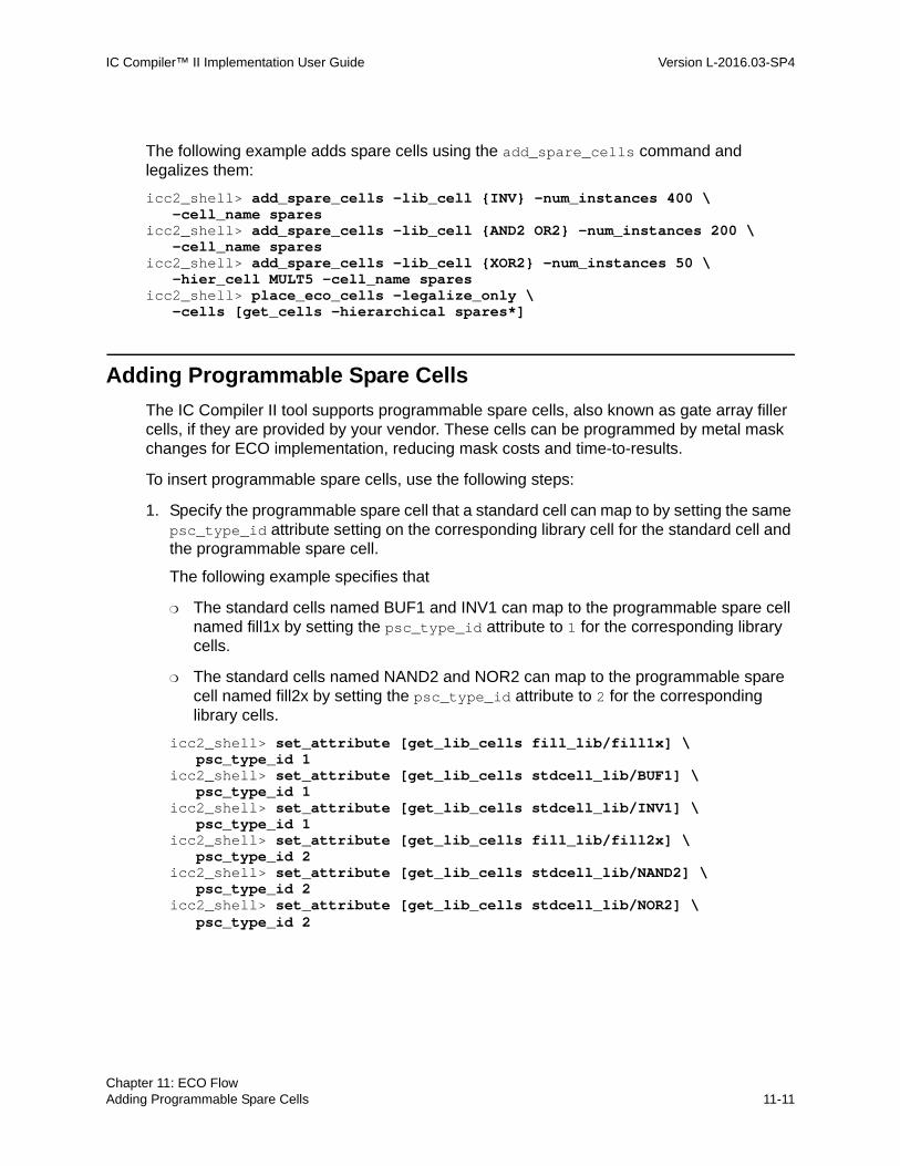
IC Compiler™ II Implementation User Guide Version L-2016.03-SP4
The following example adds spare cells using the add_spare_cells command and legalizes them:
icc2_shell> add_spare_cells -lib_cell {INV} -num_instances 400 \-cell_name spares
icc2_shell> add_spare_cells -lib_cell {AND2 OR2} -num_instances 200 \-cell_name spares
icc2_shell> add_spare_cells -lib_cell {XOR2} -num_instances 50 \-hier_cell MULT5 -cell_name spares
icc2_shell> place_eco_cells -legalize_only \ -cells [get_cells -hierarchical spares*]
Adding Programmable Spare Cells
The IC Compiler II tool supports programmable spare cells, also known as gate array filler cells, if they are provided by your vendor. These cells can be programmed by metal mask changes for ECO implementation, reducing mask costs and time-to-results.
To insert programmable spare cells, use the following steps:
1. Specify the programmable spare cell that a standard cell can map to by setting the same psc_type_id attribute setting on the corresponding library cell for the standard cell and the programmable spare cell.
The following example specifies that
❍ The standard cells named BUF1 and INV1 can map to the programmable spare cell named fill1x by setting the psc_type_id attribute to 1 for the corresponding library cells.
❍ The standard cells named NAND2 and NOR2 can map to the programmable spare cell named fill2x by setting the psc_type_id attribute to 2 for the corresponding library cells.
icc2_shell> set_attribute [get_lib_cells fill_lib/fill1x] \ psc_type_id 1
icc2_shell> set_attribute [get_lib_cells stdcell_lib/BUF1] \ psc_type_id 1
icc2_shell> set_attribute [get_lib_cells stdcell_lib/INV1] \ psc_type_id 1
icc2_shell> set_attribute [get_lib_cells fill_lib/fill2x] \ psc_type_id 2
icc2_shell> set_attribute [get_lib_cells stdcell_lib/NAND2] \ psc_type_id 2
icc2_shell> set_attribute [get_lib_cells stdcell_lib/NOR2] \ psc_type_id 2
Chapter 11: ECO FlowAdding Programmable Spare Cells 11-11Chapter 11: ECO FlowAdding Programmable Spare Cells 11-11

IC Compiler™ II Implementation User Guide L-2016.03-SP4IC Compiler™ II Implementation User Guide Version L-2016.03-SP4
2. Insert the programmable spare cells by using the create_stdcell_fillers command.
The following example inserts programmable spare cells named fill1x and fill2x:
icc2_shell> create_stdcell_fillers \ -lib_cells {fill_lib/fill1x fill_lib/fill2x}
During the ECO flow, the tool swaps an ECO cell with a programmable spare cell based on the psc_type_id attribute setting, cell width, and voltage area. If the tool removes an ECO cell from the design, it can reuse the corresponding programmable spare cell.
Making ECO Changes Using the eco_netlist Command
You can make ECO changes to a block by using the eco_netlist command.
If you are using the freeze silicon ECO flow, enable ECO changes in the freeze silicon mode by setting the design.eco_freeze_silicon_mode application option to true, before you run the eco_netlist command.
When you use the eco_netlist command, use one of the following two methods to make the ECO changes:
• Specify a golden Verilog netlist that includes the ECO changes by using the -by_verilog_file option
• Specify a golden block that includes the ECO changes by using the -block option
When you use the -block option, by default,
❍ The tool assumes the golden block is in the current design library.
To specify a different design library, use the -golden_lib option.
❍ The tool makes the ECO changes to the current design.
To make the ECO changes to a different design, use the -working_block option. To specify the design library that contains the design specified by the -working_block option, use the -working_lib option.
The tool compares the working design to the input Verilog netlist or the golden design and generates a change file containing netlist editing Tcl commands that implements the functional changes. You must specify the name of the output file by using the -write_changes option.
Chapter 11: ECO FlowMaking ECO Changes Using the eco_netlist Command 11-12

IC Compiler™ II Implementation User Guide Version L-2016.03-SP4
By default, the tool ignores the following:
• Differences in the physical-only cells
To consider the differences in the physical-only cells, use the -compare_physical_only_cells option.
• Timing ECO changes, such as cells that are resized or repeaters that are added or removed.
To consider the timing ECO changes, in addition to the functional ECO changes, use the -extract_timing_eco_changes option.
• Differences in power and ground objects.
To make the ECO changes to the working design, source the change file that the eco_netlist command generates, as shown in the following example:
icc2_shell> eco_netlist -by_verilog_file eco.v \-compare_physical_only_cells -write_changes eco_changes.tcl
icc2_shell> source eco_changes.tcl
Comparing Netlist Differences Across Physical Hierarchy
By default, the eco_netlist command does not compare netlist differences across physical hierarchy. To compare netlist differences across physical hierarchy, set the -cross_physical_hierarchy option to true. This allows you to update the design with changes at different levels of the physical hierarchy.
When you use the option setting, you must also specify a directory name by using the -write_changes_per_module option, which is used to generate the Tcl files required for updating the design. This directory contains the following:
• A subdirectory for each level of the physical hierarchy, which contains
❍ A Tcl file for each block in that level of hierarchy, containing the netlist editing commands for incorporating the ECO changes
❍ A Tcl file named source_sequence.tcl which sources the block Tcl files for that hierarchy in the correct sequence
• A Tcl file named full_chip_source_sequence.tcl, which sources all the block-level Tcl files generated for the entire hierarchy in the correct sequence.
Chapter 11: ECO FlowMaking ECO Changes Using the eco_netlist Command 11-13Chapter 11: ECO FlowMaking ECO Changes Using the eco_netlist Command 11-13

IC Compiler™ II Implementation User Guide L-2016.03-SP4IC Compiler™ II Implementation User Guide Version L-2016.03-SP4
Figure 11-3 Hierarchy of the Design Example
For example, assume you use the following command to compare the netlist differences for a design with a hierarchy as shown in Figure 11-3:
icc2_shell> eco_netlist –by_verilog_file TOP_golden.v \ –cross_physical_hierarchy –write_changes_per_module TOP_change_dir
The tool generates a directory and file structure as follows:
• TOP_change_dir/
❍ full_chip_source_sequence.tcl
❍ top/
■ source_sequence.tcl
■ top.tcl
■ T1.tcl
■ T2.tcl
❍ A/
■ source_sequence.tcl
■ A.tcl
■ A1.tcl
■ A2.tcl
Chapter 11: ECO FlowMaking ECO Changes Using the eco_netlist Command 11-14
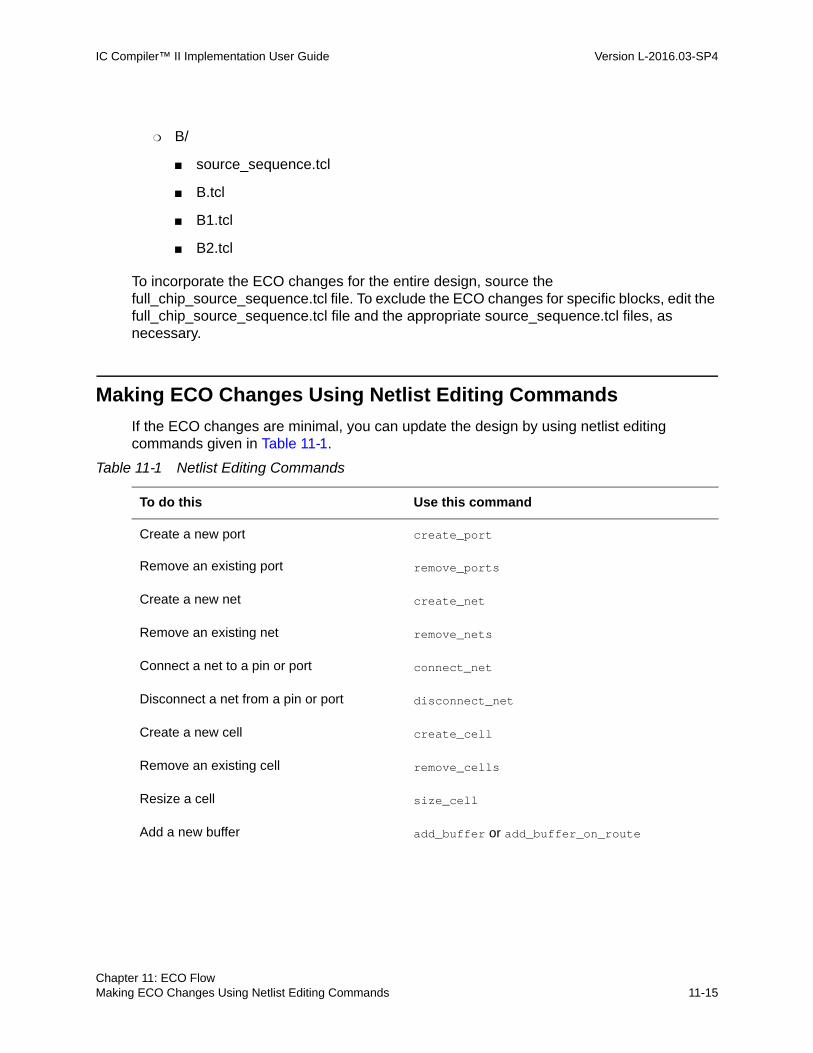
IC Compiler™ II Implementation User Guide Version L-2016.03-SP4
❍ B/
■ source_sequence.tcl
■ B.tcl
■ B1.tcl
■ B2.tcl
To incorporate the ECO changes for the entire design, source the full_chip_source_sequence.tcl file. To exclude the ECO changes for specific blocks, edit the full_chip_source_sequence.tcl file and the appropriate source_sequence.tcl files, as necessary.
Making ECO Changes Using Netlist Editing Commands
If the ECO changes are minimal, you can update the design by using netlist editing commands given in Table 11-1.
Table 11-1 Netlist Editing Commands
To do this Use this command
Create a new port create_port
Remove an existing port remove_ports
Create a new net create_net
Remove an existing net remove_nets
Connect a net to a pin or port connect_net
Disconnect a net from a pin or port disconnect_net
Create a new cell create_cell
Remove an existing cell remove_cells
Resize a cell size_cell
Add a new buffer add_buffer or add_buffer_on_route
Chapter 11: ECO FlowMaking ECO Changes Using Netlist Editing Commands 11-15Chapter 11: ECO FlowMaking ECO Changes Using Netlist Editing Commands 11-15

IC Compiler™ II Implementation User Guide L-2016.03-SP4IC Compiler™ II Implementation User Guide Version L-2016.03-SP4
Using Netlist Editing Commands in the Freeze Silicon Mode
If you are using the freeze silicon ECO flow, enable ECO changes in the freeze silicon mode by setting the design.eco_freeze_silicon_mode application option to true, before you run the netlist editing commands.
When you run the size_cell command in the freeze silicon mode, by default, the tool checks if a compatible spare cell is available within a distance of five times the unit site height before sizing the cell. If a compatible spare cell is not available, the tool does not size the cell.
• To control this distance, use the -max_distance_to_spare_cell option.
• To disable this feature, use the -not_spare_cell_aware option.
Making Netlist Edits on Modules
You do not need to uniquify the design before you use the netlist editing commands. For design with multiply instantiated modules, apply the netlist editing commands to a module by using the edit_module command, as shown in the following example:
icc2_shell> edit_module [get_module add_block] { \change_link [get_cells U25] AND2 \
change_link [get_cells U61] XOR2 }
Reverting Sized Cells
To revert the ECO changes made with the size_cell command, use the revert_cell_sizing command. To include the sized cells that are adjacent to the specified cell in the same row, use the -include_adjacent_sized_cells option. When you use this option, by default, the tool also reverts the cells that abut the specified cell on either side, if they are also sized cells. However, if you use the -adjacent_cell_distance option, the tool recursively reverts the sized cells that are adjacent to sized cells within the specified distance in the same row.
Remove an existing buffer remove_buffers
To change the reference of an existing cell change_link
Table 11-1 Netlist Editing Commands (Continued)
To do this Use this command
Chapter 11: ECO FlowMaking ECO Changes Using Netlist Editing Commands 11-16

IC Compiler™ II Implementation User Guide Version L-2016.03-SP4
Placing ECO Cells
For the unconstrained ECO flow, place the ECO cells by using the place_eco_cells command. This command derives the placement of each ECO cell based on the connectivity and the delays associated with the cell. The tool then legalizes each ECO cell to the closest unoccupied site. The existing cells are untouched to minimize the impact to their placement.
To place
• All unplaced cells, use the -unplaced_cells option.
• Specific cells, use the -cells option.
• Only the cells that have changed due to ECO operations, use the -eco_changed_cells option.
A cell is considered changed if the eco_change_status attribute of the cell has one of the following values:
❍ create_cell
❍ change_link
❍ add_buffer
❍ size_cell
When you run the eco_netlist command, the tool automatically sets the eco_change_status attribute on the changed cells. If you update the design without using the eco_netlist command, you can manually set the eco_change_status attribute by using the set_attribute command.
Chapter 11: ECO FlowPlacing ECO Cells 11-17Chapter 11: ECO FlowPlacing ECO Cells 11-17

IC Compiler™ II Implementation User Guide L-2016.03-SP4IC Compiler™ II Implementation User Guide Version L-2016.03-SP4
Controlling Placement When Using the place_eco_cells Command
The place_eco_cells command places and legalizes each ECO cell based on the connectivity and the delays associated with the cell.
You can control the placement of the ECO cells as follows:
• To use the channels areas between macro cells for ECO placement, use the -channel_aware option.
By default, the command avoids channel areas during ECO placement.
• To place ECO cells closer to fixed points, such as I/O pads or macro cells, specify a weight for the nets connected to the fixed cells by using the -fixed_connection_net_weight option.
By default, nets connected to fixed cells have a weight of one. To place ECO cells closer to fixed points, specify an integer value greater than one for the corresponding net.
• To prioritize specific nets during ECO placement by specifying net weights,
1. Specify net weights by using the set_eco_placement_net_weight command.
2. Specify that the tool honors the net weights by using the -honor_user_net_weight option with the place_eco_cells command.
To report the net weights you specify, use the report_eco_placement_net_weight command.
• To create virtual connections for ECO cells and use them during ECO placement, instead of the actual connections,
1. Create virtual connections by using the create_virtual_connection command
2. Use these virtual connections during ECO placement by using the -use_virtual_connection option with the place_eco_cells command.
The following example creates virtual connections for the inputs and output of the cell named ECO17 and performs ECO placement using these virtual connections:
icc2_shell> create_virtual_connection -name VC_0\-pins {U1/Y ECO17/A}
icc2_shell> create_virtual_connection -name VC_1\-pins {U2/Y ECO17/B}
icc2_shell> create_virtual_connection -name VC_2\-pins {ECO17/Y D17_OUT} -weight 3
icc2_shell> place_eco_cells -cells ECO17 -use_virtual_connection
Chapter 11: ECO FlowPlacing ECO Cells 11-18

IC Compiler™ II Implementation User Guide Version L-2016.03-SP4
To remove virtual connections you have created, use the remove_virtual_connections command. To query virtual connections, use the get_virtual_connections command.
• To ignore high-fanout nets connected to ECO cells that exceed a specific threshold, use the -max_fanout option with the place_eco_cells command.
• To ignore the connections of specific pins on ECO cells, use the -ignore_pin_connection option with the place_eco_cells command.
Controlling Legalization When Using the place_eco_cells Command
After placing the ECO cells, the place_eco_cells command legalizes each ECO cell to the closest unoccupied site. The existing cells are untouched to minimize the impact to their placement.
You can control the legalization of the ECO cells by using one of the following methods:
• To not legalize the cells after ECO placement, use the -no_legalize option.
• To perform legalization only, use the -legalize_only option.
• To specify the mode in which to legalize, use the -legalize_mode option with one of the following settings:
❍ free_site_only
When you specify this setting, the default, the tool legalizes the ECO cells on free sites without moving preexisting cells. An ECO cells can have a large displacement, if a free site is unavailable nearby.
❍ allow_move_other_cells
When you specify this setting, the tool legalizes the ECO cells to the nearest legal location by moving preexisting cells.
❍ minimum_physical_impact
When you specify this setting, the tool first legalizes the ECO cells the can be legalized to a free site nearby without moving preexisting cells. For the ECO cells that do not have a free site nearby, the tool legalizes them by moving preexisting cells.
• To specify a displacement threshold for legalization, use the -displacement_threshold option.
When you use the -displacement_threshold option, you can also use the -max_displacement_threshold option to specify a second displacement threshold that is larger than the value specified with the -displacement_threshold option.
Chapter 11: ECO FlowPlacing ECO Cells 11-19Chapter 11: ECO FlowPlacing ECO Cells 11-19

IC Compiler™ II Implementation User Guide L-2016.03-SP4IC Compiler™ II Implementation User Guide Version L-2016.03-SP4
How the tool uses these displacement thresholds depends on the setting you use for the -legalize_mode option as follows:
❍ free_site_only
When you specify this setting, the tool legalizes the ECO cells that have available free sites within the specified displacement threshold.
If the displacement of an ECO cell exceeds this threshold, the tool does not legalize the cell. It creates a collection named epl_legalizer_rejected_cells that consists of such ECO cells that are not legalized.
You can subsequently legalize the ECO cells in the epl_legalizer_rejected_cells collection by using the following command:
icc2_shell> place_eco_cells -legalize_mode allow_move_other_cells \-legalize_only -cells $epl_legalizer_rejected_cells
This command moves existing cells to find legal locations for the ECO cells in the collection named epl_legalizer_rejected_cells.
If you also specify the -max_displacement_threshold option with -displacement_threshold option, the tool also creates a collection named epl_max_displacement_cells that consists of ECO cells with a displacement larger than that specified by this option. The collection epl_max_displacement_cells is a subset of the collection epl_legalizer_rejected_cells and its cells are also not legalized.
You can use the -max_displacement_threshold option to identify ECO cells with a very large displacement, for which you want to reject the ECO changes.
❍ allow_move_other_cells
When you specify this setting, you cannot specify the -displacement_threshold and -max_displacement_threshold options.
❍ minimum_physical_impact
When you specify this setting, the tool first legalizes the ECO cells that have available free sites within the specified displacement threshold.
If the displacement of an ECO cell exceeds this threshold, the tool legalizes them by moving preexisting cells.
If you also specify the -max_displacement_threshold option, the tool does not legalize the cells that exceed this maximum displacement threshold specified with this option and the tool creates a collection named epl_max_displacement_cells that consists of ECO cells with a displacement larger than that specified by this option. You can use the -max_displacement_threshold option to identify ECO cells with a very large displacement, for which you want to reject the ECO changes.
Chapter 11: ECO FlowPlacing ECO Cells 11-20

IC Compiler™ II Implementation User Guide Version L-2016.03-SP4
• To specify the types of filler cells that can be removed during legalization, use the -remove_filler_references option.
When you use this option, the filler cells are removed if they do not have a fixed placement and they overlap with ECO cells. By default, the tool does not remove any filler cells when legalizing ECO cells.
Placing and Mapping ECO Cells to Spare Cells
For the freeze silicon ECO flow, place and map the ECO cells to spare cells by using the place_freeze_silicon command. By default, this command places and maps all ECO cells. To place and map specific ECO cells, use the -cells option. The following example places and maps the ECO cells named ECO1, ECO2, and ECO3:
icc2_shell> place_freeze_silicon -cells {ECO1 ECO2 ECO3}
This command places each ECO cell and maps it to the nearest matching spare cell. Cells that are deleted as a result of the ECO changes are not removed from the design. They are converted to spare cells and remain in the design.
When you use the place_freeze_silicon command, you can
• Place the ECO cells by the target spare cells, but not map them to the spare cells, by using the -no_spare_cell_swapping option
This feature allows you to place the ECO cells and analyze the QoR before you map them.
• Map the spare cells that are already placed by the target spare cells by using the -map_spare_cells_only option.
• Generate an ECO cell to spare cell mapping file by using the -write_map_file command.
You can edit the mapping file, if necessary, and map the ECO cells by using the map_freeze_silicon command.
Mapping ECO Cells to Specific Spare Cells
To map an ECO cell to a specific spare cell, use the map_freeze_silicon command. Specify the ECO cell name and the corresponding spare cell name by using the -eco_cell and -spare_cell options. The following example maps the ECO cell named ECO1 to the spare cell named spare_1:
icc2_shell> map_freeze_silicon -eco_cell ECO1 -spare_cell spare_1
Chapter 11: ECO FlowPlacing and Mapping ECO Cells to Spare Cells 11-21Chapter 11: ECO FlowPlacing and Mapping ECO Cells to Spare Cells 11-21

IC Compiler™ II Implementation User Guide L-2016.03-SP4IC Compiler™ II Implementation User Guide Version L-2016.03-SP4
You can specify the ECO cell to spare cell mapping by using a map file and specifying this map file name by using the -map_file option with the map_freeze_silicon command. The map file has the following format:
ECO_cell_1 spare_cell_1ECO_cell_2 spare_cell_2... ...
Updating Supply Nets for ECO Cells
To update the supply nets for ECO cells, use the eco_update_supply_net command. By default, it updates the supply nets for all cell added by using the following ECO commands:
• size_cell in freeze-silicon mode
• add_buffer
• add_eco_repeater
• split_fanout
• add_buffer_on_route
To update the supply nets for specific cells, use the eco_update_supply_net -cells command.
Performing ECO Routing
If the changes are minimal and are limited to a few layers. you can manually route the nets changed by the ECO process.
When the change is large, use the route_eco command to route the affected nets. This command routes all open nets and newly added nets, and cleans up the deleted nets, obsolete nets, and unused sections of changed wires.
By default, the route_eco command reroutes any noncritical net to fix routing DRC violations. As a result, nets that are unchanged by the ECO process might be rerouted. This default behavior is suitable when there are many ECO changes.
To control the rerouting of nets unchanged by the ECO process, use the following option settings with the route_eco command:
• To route the ECO nets first and reroute the other nets only for fixing routing DRC violations, use the -reroute modified_nets_first_then_others option.
This reduces the layout changes and is suitable when the there are only a small number of ECO changes.
Chapter 11: ECO FlowUpdating Supply Nets for ECO Cells 11-22

IC Compiler™ II Implementation User Guide Version L-2016.03-SP4
• To route only the ECO nets, use the -reroute modified_nets option.
This is very restrictive and can result in the tool being unable to fix all routing DRC violations. As a result, it should be used only when there are only a very few ECO changes.
See Also
• Unconstrained ECO Flow
• Freeze Silicon ECO Flow
Adding Buffers on Routed Nets
During the timing ECO flow, to add buffers or pairs of inverters on a fully routed net, use the add_buffer_on_route command.
When you use this command, you must specify what cells, buffers, or pairs of inverters to add and where to add them by using one of the following methods:
• Specify an exact configuration of cells and their locations by using the -user_specified_buffers option.
With -user_specified_buffers option, you can add cells only on one net at a time. You can insert different types of buffers or inverter pairs by using this option, but you cannot combine both buffers and inverter pairs.
For each cell you add, you must specify the instance name, the library cell to use, the x- and y-coordinates of the exact location, and a layer at that location with an existing routing shape to connect to by using the {name1 lib_cel1 x1 y1 layer1.... } format.
Alternatively, you can specify only the instance name, the library cell to use, and the x- and y-coordinates for the location, by using the {name1 lib_cel1 x1 y1 .... } format, and use the -detect_layer option to have the tool automatically detect the closest routing shape to that location.
The following example adds two cells named ECO1 and ECO2 on net n22. The ECO1 cell is of type BUF2, at location (100, 70), connecting to a routing shape on the M3 layer. The ECO2 cell is of type BUF4, at location (150, 70), also connecting to a routing shape on the M3 layer.
icc2_shell> add_buffer_on_route net22 \-user_specified_buffers {ECO1 BUF2 100 70 M3 ECO2 BUF4 150 70 M3}
• Specify a list one or more library cells to select from by using the -lib_cell option and the exact locations by using the -location option.
Chapter 11: ECO FlowAdding Buffers on Routed Nets 11-23Chapter 11: ECO FlowAdding Buffers on Routed Nets 11-23

IC Compiler™ II Implementation User Guide L-2016.03-SP4IC Compiler™ II Implementation User Guide Version L-2016.03-SP4
With -location option, you can add cells only on one net at a time.
For the exact location, you must specify the x- and y-coordinates and a layer with an existing routing shape at that location to connect the cell to by using the {x1 y1 layer1 ....} format.
Alternatively, you can specify only the x- and y-coordinates for the location, by using the {x1 y1 ...} format, and use the -detect_layer option to have the tool automatically detect the closest routing shape to that location.
The following example adds the mylib/BUF1 library cell on the net1 net at location (100, 200) and connects it to an existing route shape on the M4 layer.
icc2_shell> add_buffer_on_route net1 -lib_cell mylib/BUF1 \-location {100 200 M4}
• Specify a list one or more library cells to select from by using the -lib_cell option and the distance between the cells by using the -repeater_distance option.
With the -repeater_distance option, you can add buffers on one or more nets. To specify the distance in microns between the driver of the net and the first repeater cell, use the -first_distance option.
You can scale the distance between the cells by
❍ Specifying a different distance scaling factor for each layer. To do so use the -scaled_by_layer option.
❍ Using the ratio between the default width for the layer and the actual route width as the distance scaling factor by specifying the -scaled_by_width option.
The following example adds the mylib/BUF1 library cell as a repeater cell on the nets n2 and n5 at an interval of 150 microns. The distance between the driver and the first repeater cell is 100 microns.
icc2_shell> add_buffer_on_route {n2 n5} -lib_cell mylib/BUF1 \-first_distance 100 -repeater_distance 150
• Specify a list one or more library cells to select from by using the -lib_cell option and the distance between the cells as a ratio of the total net length by using the -repeater_distance_length_ratio option.
To specify the distance between the repeater cells as a ratio of the total net length, use the -repeater_distance_length_ratio option.
With the -repeater_distance_length_ratio option, you can add buffers on one or more nets. To specify the distance between the driver and the first repeater as a ratio of the total net length, use the -first_distance_length_ratio option.
The following example adds the mylib/BUF1 library cell as a repeater cell on the nets n3, n21, and n41 at an interval that is 20 percent of the total net length. The distance between the driver and the first repeater cell is 10 percent of the total net length.
Chapter 11: ECO FlowAdding Buffers on Routed Nets 11-24

IC Compiler™ II Implementation User Guide Version L-2016.03-SP4
icc2_shell> add_buffer_on_route {n3 n21 n41} -lib_cell mylib/BUF1 \-first_distance_length_ratio 0.1 \ -repeater_distance_length_ratio 0.2
By default, the add_buffer_on_route command
• Uses eco_net as the name prefix for all new nets and eco_cell as the name prefix for all new cells.
To specify a name prefix for new nets and cells, use the -net_prefix and -cell_prefix options, respectively.
• Adds repeater cells over all placement blockages, soft macros, and hard macros.
To prevent repeaters from being placed over specific macro cells, use the -dont_allow_insertion_over_cell option.
Alternatively, you can prevent the repeaters from being placed over all blockages and macro cells by using the -respect_blockages option. When you use this option, you can specify a list of macro cells over which buffers are allowed by using the -allow_insertion_over_cell option.
• Adds repeater cells on both global routed and detail routed nets.
To add cells only on nets that are global routed only, without assigned tracks or detail routing, use the -only_global_routed_nets option.
• Adds buffers at the lowest common level of hierarchy of the pins being driven by the buffers.
To add the buffers on the highest possible level of hierarchy, use the -on_top_hierarchy option.
• Does not add repeater cells on a route segment if it is necessary to create new ports because of a difference in the logical and physical topology of the net.
To add repeaters on such route segments by creating new ports, use the -punch_port option.
For multivoltage designs, you can consider the multivoltage settings and constraints as follows:
• To ensure that primary and secondary voltage areas are honored and cells are added in logical hierarchies that are physically in the corresponding voltage areas, use the -respect_voltage_areas option.
• To specify different library cells for different voltage areas, use the -voltage_area_specific_lib_cells option and specify the list library cells using the {va1 lib_cell1 va2 lib_cel2 ...} format.
When you use this option, you must also use the -lib_cell option.
Chapter 11: ECO FlowAdding Buffers on Routed Nets 11-25Chapter 11: ECO FlowAdding Buffers on Routed Nets 11-25

IC Compiler™ II Implementation User Guide L-2016.03-SP4IC Compiler™ II Implementation User Guide Version L-2016.03-SP4
• To allow buffers on physical feedthrough nets of a voltage area, specify the voltage areas with the -allow_physical_feedthrough_buffer option.
This option can only be used with the -respect_voltage_areas or -voltage_area_specific_lib_cells option, and the voltage area you specify must be a primary voltage area.
After you run the add_buffer_on_route command with this option, update the supply net and power domain setting for the added buffers by using the set_eco_power_intention command.
• To add cells within gas stations of specified supply nets, use the -respect_gas_station option and specify the supply net.
Gas stations are areas with a constant power supply. These areas used for buffering nets that go through power domains that are powered down.
To specify the maximum allowed distance from the gas station to the added buffer, use the -max_distance_route_to_gas_station option.
When you set the design.eco_freeze_silicon_mode application option to true and run the add_buffer_on_route command in the freeze silicon mode, the tool checks if a spare cell is available within a distance of five times the unit site height before adding a buffer. If a spare cell is not available, the tool does not add the buffer.
• To control this distance, use the -max_distance_to_spare_cell option.
• To disable this feature, use the -not_spare_cell_aware option.
Optimizing the Fanout of a Net
During the timing ECO flow, you can add buffers to a net and optimize its fanout by using the split_fanout command.
With this command, you must specify
• The net to optimize by specifying its name by using the -net option or its driver by using the -driver option
• The library cell to use by using the -lib_cell option
• The method in which to optimize the net by specifying one of the following:
❍ A maximum fanout constraints for the net by using the -max_fanout option
❍ The load pins or ports to buffer by using the -load option
When you use this option, you can specify the logical hierarchy to add the buffer by using the -hierarchy option.
Chapter 11: ECO FlowOptimizing the Fanout of a Net 11-26

IC Compiler™ II Implementation User Guide Version L-2016.03-SP4
In addition, you can
• Add the buffers on the existing route topology of the net by using the -on_route option
If you use this option with the -load option, you cannot specify the -hierarchy option.
• Avoid placement blockages and macro cells when placing buffers by using the -respect_blockages option
• Specify a name prefix for the new cells and nets by using -cell_prefix and -net_prefix options
By default, the tool uses eco_cell and eco_net as the name prefix for the new cells and nets.
Recording the Changes Made to a Layout
You can record the changes you make to a layout and generate a Tcl file containing the changes by using the record_layout_editing command, as shown in the following example:
icc2_shell> record_layout_editing -starticc2_shell> remove_shapes RECT_32_0icc2_shell> record_layout_editing -stop -output layout_changes1.tcl
You can make the following layout changes:
• Create or remove layout objects by using Tcl commands
• Set attributes by using the set_attribute command
• Move or resize objects by using the GUI
With this feature, multiple users can make ECO changes to different parts of a layout in parallel. Each user can output a Tcl file that contains the layout changes they make by using the record_layout_editing command, and all the Tcl files can be applied to the original layout.
Chapter 11: ECO FlowRecording the Changes Made to a Layout 11-27Chapter 11: ECO FlowRecording the Changes Made to a Layout 11-27

IC Compiler™ II Implementation User Guide L-2016.03-SP4IC Compiler™ II Implementation User Guide Version L-2016.03-SP4
Chapter 11: ECO FlowRecording the Changes Made to a Layout 11-28