ia64f3048sec1 security-enhanced microcontroller (3.3 v) data
TRANSCRIPT
IA64F3048SEC2 Data Sheet Security-Enhanced Microcontroller (3.3 V) October 7, 2008
Copyright 2008 DOCUMENT # IA211040405-02 www.Innovasic.com
Customer Support:
Page 1 of 63 1-888-824-4184
©
IA64F3048SEC1 Security-Enhanced Microcontroller (3.3 V)
Data Sheet

IA64F3048SEC2 Data Sheet Security-Enhanced Microcontroller (3.3 V) October 7, 2008
Copyright 2008 DOCUMENT # IA211040405-02 www.Innovasic.com
Customer Support:
Page 2 of 63 1-888-824-4184
©
Copyright © 2008 by Innovasic Semiconductor, Inc.
Published by Innovasic Semiconductor, Inc.
3737 Princeton Drive NE, Suite 130, Albuquerque, NM 87106 Innovasic Semiconductor, Inc. Office: 505.883.5263 3737 Princeton Drive NE, Suite 130 FAX: 505.883.5477 Albuquerque, NM 87107-4237 Toll Free: 1-888.824.4184
www.innovasic.com An ISO 9001:2000 Company Cygwin
® is a registered trademark of Red Hat, Inc.
H8® is a registered trademark of Renesas Technology Corporation.
Linux® is the registered trademark of Linus Torvalds.
Microsoft®, Windows
®, and Windows NT
® are registered trademarks of Microsoft Corporation.

IA64F3048SEC2 Data Sheet Security-Enhanced Microcontroller (3.3 V) October 7, 2008
Copyright 2008 DOCUMENT # IA211040405-02 www.Innovasic.com
Customer Support:
Page 3 of 63 1-888-824-4184
©
Table of Contents Please Note...................................................................................................................................... 6
Overview ......................................................................................................................................... 6
Features ....................................................................................................................................... 6
Compatibility .............................................................................................................................. 7
Software Development Tools ..................................................................................................... 7
Added Features ........................................................................................................................... 7
Functional Blocks ....................................................................................................................... 8
Central Processing Unit (CPU) ..................................................................................................... 10
Microcontroller Operating Modes ................................................................................................ 10
Flash Memory ............................................................................................................................... 12
Mode Pin Settings ..................................................................................................................... 13
Internal RAM ................................................................................................................................ 16
32-Bit x 32-Bit Multiply ............................................................................................................... 17
Hardware Random Number Generator ......................................................................................... 18
Features ..................................................................................................................................... 18
Input/Output Ports ......................................................................................................................... 19
Interrupt Controller ....................................................................................................................... 20
Exception Sources ..................................................................................................................... 20
Bus Controller ............................................................................................................................... 21
Features ..................................................................................................................................... 21
Refresh Controller ......................................................................................................................... 21
Direct Access Memory Controller (DMAC) ................................................................................ 22
Serial Communication Interface (SCI) ......................................................................................... 22
Smart Card Interface ..................................................................................................................... 23
Analog-to-Digital Converter (ADC) ............................................................................................. 24
Digital-to-Analog Converter (DAC) ............................................................................................. 25
DAC Pin Descriptions............................................................................................................... 25
Integrated Timer Unit (ITU) ......................................................................................................... 26
Programmable Timing Pattern Controller .................................................................................... 26
Watchdog Timer (WDT)............................................................................................................... 26
Pinout ............................................................................................................................................ 27
Electrical Characteristics .............................................................................................................. 32
Absolute Maximum Ratings ..................................................................................................... 32
DC Characteristics .................................................................................................................... 32
Permissible Output Currents ..................................................................................................... 35
AC Characteristics .................................................................................................................... 37
Physical Dimensions ..................................................................................................................... 60
Ordering Information .................................................................................................................... 62
Errata ............................................................................................................................................. 63

IA64F3048SEC2 Data Sheet Security-Enhanced Microcontroller (3.3 V) October 7, 2008
Copyright 2008 DOCUMENT # IA211040405-02 www.Innovasic.com
Customer Support:
Page 4 of 63 1-888-824-4184
©
List of Figures Figure 1. IA64F3048SEC1 Security-Enhanced Microcontroller Block Diagram .......................... 9
Figure 2. IA64F3048SEC1 Memory Map .................................................................................... 11
Figure 3. 128-Kbyte Flash Memory A and Security Bits Map ..................................................... 12
Figure 4. IA64F3048SEC1 Pinout ................................................................................................ 27
Figure 5. Darlington Pair Drive Circuit Example ......................................................................... 36
Figure 6. LED Drive Circuit Example .......................................................................................... 36
Figure 7. Output Load Circuit ....................................................................................................... 37
Figure 8. Basic Bus Cycle, Two-State Access .............................................................................. 40
Figure 9. Basic Bus Cycle, Three-State Access ............................................................................ 41
Figure 10. Basic Bus Cycle, Three-State Access with One Wait State ........................................ 42
Figure 11. DRAM Bus Timing, Read/Write, Three-State Access, 2we_n Mode ......................... 44
Figure 12. DRAM Bus Timing, Refresh Cycle, Three-State Access, 2we_n Mode .................... 45
Figure 13. DRAM Bus Timing, Self-Refresh Mode, 2we_n Mode.............................................. 46
Figure 14. DRAM Bus Timing, Read/Write, Three-State Access, 2cas_n Mode ........................ 47
Figure 15. DRAM Bus Timing, Refresh Cycle, Three-State Access, 2cas_n Mode .................... 48
Figure 16. DRAM Bus Timing, Self-Refresh Mode, 2we_n Mode.............................................. 49
Figure 17. PSRAM Bus Timing, Read/Write, Three-State Access .............................................. 50
Figure 18. PSRAM Bus, Refresh Cycle........................................................................................ 51
Figure 19. Oscillator Settling Time .............................................................................................. 52
Figure 20. Reset Input Timing ...................................................................................................... 53
Figure 21. Interrupt Input Timing ................................................................................................. 53
Figure 22. Bus-Release Mode Timing .......................................................................................... 54
Figure 23. Direct Memory Access Controller (DMAC) dreq_n Input Timing ............................. 56
Figure 24. DMAC tend_n Output Timing, Two-State Access ..................................................... 56
Figure 25. DMAC tend_n Output Timing, Three-State Access ................................................... 57
Figure 26. Integrated Timer Unit (ITU) Timing ........................................................................... 57
Figure 27. ITU External Clock Input Timing ............................................................................... 58
Figure 28. Serial Communication Interface (SCI) sck Input Clock Timing ................................. 58
Figure 29. SCI Input/Output Timing, Synchronous Mode ........................................................... 59
Figure 30. SCI Timing Pattern Controller (TPC) and I/O Port Timing ........................................ 59
Figure 31. IA64F3048SEC1 100-Lead TQFP Physical Dimensions............................................ 60

IA64F3048SEC2 Data Sheet Security-Enhanced Microcontroller (3.3 V) October 7, 2008
Copyright 2008 DOCUMENT # IA211040405-02 www.Innovasic.com
Customer Support:
Page 5 of 63 1-888-824-4184
©
List of Tables
Table 1. Operating Mode and Flash Memory ............................................................................... 13
Table 2. Memory Read Mode Characteristics .............................................................................. 14
Table 3. Flash Memory Characteristics ........................................................................................ 15
Table 4. MLTXS.L Operand Format and Number of States for Execution ................................. 17
Table 5. MLTXU.L Operand Format and Number of States for Execution ................................. 17
Table 6. ADC Conversion Characteristics .................................................................................... 24
Table 7. DAC Conversion Characteristics .................................................................................... 25
Table 8. Mode Pin Settings and Operating Mode ......................................................................... 29
Table 9. Absolute Maximum Ratings ........................................................................................... 32
Table 10. DC Characteristics—Part 1 ........................................................................................... 33
Table 11. DC Characteristics—Part 2 ........................................................................................... 34
Table 12. Permissible Output Currents ......................................................................................... 35
Table 13. Bus Timing Parameters ................................................................................................. 39
Table 14. Refresh Controller Timing Parameters ......................................................................... 43
Table 15. Refresh Controller Timing Parameters ......................................................................... 52
Table 16. On-Chip System Module Timing Parameters ............................................................... 55
Table 17. IA64F3048SEC1 100-Lead TQFP Physical Dimensions ............................................. 61
Table 18. IA64F3048SEC1 Ordering Information ....................................................................... 62

IA64F3048SEC2 Data Sheet Security-Enhanced Microcontroller (3.3 V) October 7, 2008
Copyright 2008 DOCUMENT # IA211040405-02 www.Innovasic.com
Customer Support:
Page 6 of 63 1-888-824-4184
©
Please Note
This data sheet provides only a high-level overview of the IA64F3048SEC1 Security-Enhanced
Microcontroller. For a more detailed description of the IA64F3048SEC1, please refer to the
IA64F3048SEC1 Security-Enhanced Microcontroller (3.3 V) User’s Manual.
Overview The IA64F3048SEC1 Security-Enhanced Microcontroller is the ideal solution for many
embedded applications, combining the flexibility of the H8®/300H family of microcontrollers
with the power of additional on-chip features. This combination allows the development of more
complex embedded applications than are possible with the H8® alone. It also eases the
implementation of the more robust security features that are required of products today.
Features The IA64F3048SEC1 Security-Enhanced Microcontroller includes the following features:
Hardware random number generator
Fast 32-bit x 32-bit hardware multiplier
Secure memory operation
16 Kbytes of SRAM (8K words)
1 Kbyte of flash security bits
32 Kbytes of internal data flash memory
128 Kbytes of internal program flash memory
Operation at up to 50 MHz
Sixteen 16-bit general-purpose registers
Flexible instruction set built on 62 basic instruction types
8-/16-/32-bit data transfer, arithmetic and logic instructions
Signed and unsigned multiply and divide instructions
Extensive bit manipulation instructions
Bus controller with 8- and 16-bit access
3-function refresh controller
DMA controller with short- or full-address mode
16-bit integrated timer unit with 5 channels
Programmable timing pattern controller
Watchdog timer
Serial communications interface with built-in smart card interface
Eight 10-bit A/D converter channels
Two 8-bit D/A converter channels
Clock pulse generator
Interrupt controller with 37 sources
70 input/output pins and 8 input-only pins
3.3 V operation
100-pin TQFP package
IA64F3048SEC2 Data Sheet Security-Enhanced Microcontroller (3.3 V) October 7, 2008
Copyright 2008 DOCUMENT # IA211040405-02 www.Innovasic.com
Customer Support:
Page 7 of 63 1-888-824-4184
©
Compatibility
The IA64F3048SEC1 provides an upward compatibility path for H8®/300H users who need
higher performance and on-chip security features. The IA64F3048SEC1 is code compatible with
the H8®/300H family of microcontrollers. The device is available in a 100-lead TQFP package.
Software Development Tools
The IA64F3048SEC1 software development tools are based on the popular GNU toolset of GCC.
These tools support the development of C and H8®/300 assembly language programs.
Developers can compile, assemble, and link C and H8®/300 assembly language files to produce
binary absolute files. These binary absolute files can then be downloaded or programmed into
the IA64F3048SEC1 development board for debug and testing.
The software tools support and debugging applications are downloaded into RAM with
INSIGHT and the GNU GDB debugger. GDB stubs that execute in the target as a monitor
program are provided for debugging both RAM-based and ROM-based applications.
The development board software tools include a utility for programming both the internal flash
memory of the IA64F3048SEC1 part and the external EEPROM located on the development
board.
These tools can operate in either a LINUX® environment or a Windows NT
® (Windows
® 2000,
Windows® XP PRO) environment that has the Cygwin
® toolset installed.
Added Features
The IA64F3048SEC1 offers all of the standard features of the advanced H83048 microcontroller
series, with an operating frequency of up to 50 MHz. In addition, Innovasic Semiconductor has
added new security-related features that make the IA64F3048SEC1 a compelling choice for
embedded applications requiring higher levels of integrity, authenticity, and data protection
without a loss of performance. These security features include an extremely flexible 128 Kbytes
of non-volatile memory in two independent partitions. This non-volatile memory has read-out
protection and locking mechanisms to protect vital data. Additional security enhancements
include a high-quality hardware-based random number generator.
IA64F3048SEC2 Data Sheet Security-Enhanced Microcontroller (3.3 V) October 7, 2008
Copyright 2008 DOCUMENT # IA211040405-02 www.Innovasic.com
Customer Support:
Page 8 of 63 1-888-824-4184
©
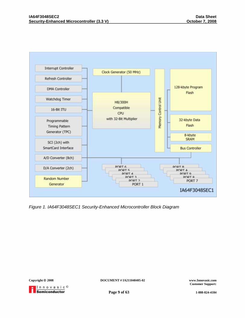
Functional Blocks
The IA64F3048SEC1 microcontroller consists of the following functional blocks:
Central Processing Unit (CPU)
Memory Control Unit (MCU)
Interrupt Controller
Bus Controller
Refresh Controller
Direct Memory Access (DMA) Controller (DMAC)
Input/Output (I/O) Ports
Integrated Timer Unit (ITU)
Programmable Timing Pattern Controller (TPC)
Watchdog Timer
Serial Communication Interface
Smart Card Interface (SCI)
Analog-to-Digital (A/D) Converter (ADC)
Digital-to-Analog (D/A) Converter (DAC)
On-Chip RAM
On-Chip 128-Kbyte Program Flash Memory
Clock Generator
32-Kbyte Data Flash memory
32-Bit x 32-Bit Hardware Multiplier (64-Bit Result)
Hardware Random Number Generator
A functional block diagram of the IA64F3048SEC1 is shown in Figure 1.
IA64F3048SEC2 Data Sheet Security-Enhanced Microcontroller (3.3 V) October 7, 2008
Copyright 2008 DOCUMENT # IA211040405-02 www.Innovasic.com
Customer Support:
Page 9 of 63 1-888-824-4184
©
Figure 1. IA64F3048SEC1 Security-Enhanced Microcontroller Block Diagram

IA64F3048SEC2 Data Sheet Security-Enhanced Microcontroller (3.3 V) October 7, 2008
Copyright 2008 DOCUMENT # IA211040405-02 www.Innovasic.com
Customer Support:
Page 10 of 63 1-888-824-4184
©
Central Processing Unit (CPU)
The IA64F3048SEC1 Security-Enhanced Microcontroller is an H8®/300 upward-compatible
microcontroller containing a 32-bit central processing unit (CPU), on-chip flash memory, on-chip
RAM, on-chip modules for serial communications, direct memory access (DMA), watchdog
timer, D/A and A/D converters, hardware-based random number generation, and other functions.
Additional features include the following:
Maximum clock frequency of 25 MHz external, with clock doubling to create up to a 50
MHz internal clock (phi clock).
Eight 32-bit general-purpose registers that can be used as sixteen 16-bit or thirty-two 8-bit
registers.
1-Mbyte or 16-Mbyte linear address space (see Figure 2).
Low power-consumption modes: Software Standby or Hardware Standby.
Microcontroller Operating Modes
The IA64F3048SEC1 Security-Enhanced Microcontroller supports seven operating modes that
determine address range, on-chip flash visibility, and initial bus mode (8-bit vs. 16-bit data). The
operating mode is selected by the state of the mode pins (md[2:0]) when the part is brought out
of reset. Valid modes are 1 through 7; Mode 0 is PROM Mode. The mode pins must not be
changed during operation.
Modes 1, 2, 3, and 4 disable internal flash and provide access to external memory or peripherals.
Modes 5 and 6 provide access to external memory, as well as on-chip flash. Mode 7 is a single-
chip mode that does not provide external memory access.

IA64F3048SEC2 Data Sheet Security-Enhanced Microcontroller (3.3 V) October 7, 2008
Copyright 2008 DOCUMENT # IA211040405-02 www.Innovasic.com
Customer Support:
Page 11 of 63 1-888-824-4184
©
Figure 2. IA64F3048SEC1 Memory Map

IA64F3048SEC2 Data Sheet Security-Enhanced Microcontroller (3.3 V) October 7, 2008
Copyright 2008 DOCUMENT # IA211040405-02 www.Innovasic.com
Customer Support:
Page 12 of 63 1-888-824-4184
©
Flash Memory
The IA64F3048SEC1 Security-Enhanced Microcontroller onboard flash memory is comprised of
three separate embedded memory blocks:
128-Kbyte Flash Memory A Block
Security Bits (SecFlash)
32-Kbyte Flash Memory B Block
The 128-Kbyte Flash Memory A Block is further partitioned as shown in Figure 3. This
particular memory block includes a 128-Kbyte memory array and a security bits memory array
that overlap the same address space.
Figure 3. 128-Kbyte Flash Memory A and Security Bits Map
IA64F3048SEC2 Data Sheet Security-Enhanced Microcontroller (3.3 V) October 7, 2008
Copyright 2008 DOCUMENT # IA211040405-02 www.Innovasic.com
Customer Support:
Page 13 of 63 1-888-824-4184
©
Note the following restrictions when using the IA64F3048SEC1:
The flash memory programming power supply is Vcc. The maximum rating of the fwe
pin is Vcc + 0.3V. Applying a voltage in excess of the maximum rating will permanently
damage the device.
Only the 128-Kbyte flash memory can be programmed with a PROM programmer (in
addition to onboard programming methods). The 32-Kbyte flash memory block can only
be programmed using the onboard programming methods.
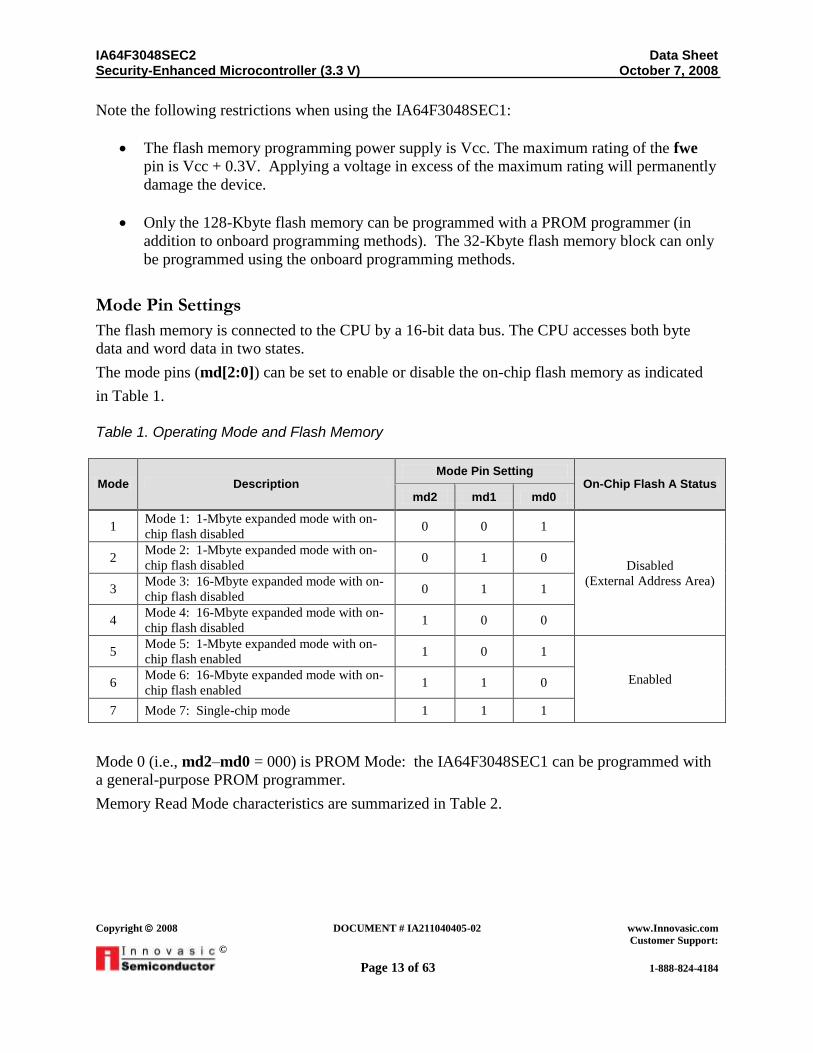
Mode Pin Settings
The flash memory is connected to the CPU by a 16-bit data bus. The CPU accesses both byte
data and word data in two states.
The mode pins (md[2:0]) can be set to enable or disable the on-chip flash memory as indicated
in Table 1.
Table 1. Operating Mode and Flash Memory
Mode Description Mode Pin Setting
On-Chip Flash A Status md2 md1 md0
1 Mode 1: 1-Mbyte expanded mode with on-
chip flash disabled 0 0 1
Disabled
(External Address Area)
2 Mode 2: 1-Mbyte expanded mode with on-
chip flash disabled 0 1 0
3 Mode 3: 16-Mbyte expanded mode with on-
chip flash disabled 0 1 1
4 Mode 4: 16-Mbyte expanded mode with on-
chip flash disabled 1 0 0
5 Mode 5: 1-Mbyte expanded mode with on-
chip flash enabled 1 0 1
Enabled 6 Mode 6: 16-Mbyte expanded mode with on-
chip flash enabled 1 1 0
7 Mode 7: Single-chip mode 1 1 1
Mode 0 (i.e., md2–md0 = 000) is PROM Mode: the IA64F3048SEC1 can be programmed with
a general-purpose PROM programmer.
Memory Read Mode characteristics are summarized in Table 2.

IA64F3048SEC2 Data Sheet Security-Enhanced Microcontroller (3.3 V) October 7, 2008
Copyright 2008 DOCUMENT # IA211040405-02 www.Innovasic.com
Customer Support:
Page 14 of 63 1-888-824-4184
©
Table 2. Memory Read Mode Characteristics
Item Symbol Min Max Unit
Command write cycle tnxtc 20 — µs
ce_n hold time tceh 5 —
ns
ce_n setup time tces 0 —
Data hold time tdh 50 —
Data setup time tds 50 —
Write pulse width twep 70 —
we_n rises time tr —
30
we_n fall time tf —
30
128-Kbyte Embedded Flash Memory A and Security Bits Features
The IA64F3048SEC1 has 128 Kbytes of on-chip Flash Memory A and 1 Kbyte of Security Flash.
The features of these flash areas are summarized below.
Three flash operating modes:
o Program Mode
o Erase Mode
o Read Mode
Memory size:
o 128-Kbyte Flash A and Security Flash arrays separately selectable
384 bytes of Security Flash reserved for security bit functions
Programming methodology: 128-byte page programmable
Programming endurance: > 20,000 cycles
Erase methodology: Block erasable on selected block sizes; no full-chip erase available
except in PROM and Boot Modes
Read methodology: 16-bit readable
Single 3.3-volt supply
Page erase time: < 40 ms
128-Kbytes flash A block sizes (4 block sizes):
o Four 1-Kbyte areas
o Two 32-Kbyte areas
o Two 28-Kbyte areas
o One 4-Kbyte area

IA64F3048SEC2 Data Sheet Security-Enhanced Microcontroller (3.3 V) October 7, 2008
Copyright 2008 DOCUMENT # IA211040405-02 www.Innovasic.com
Customer Support:
Page 15 of 63 1-888-824-4184
©
Security Flash block size:
o Three 128-byte areas
Adaptable to three programming modes:
o Programming with commercial PROM programmer
o Boot ROM Mode programming compatibility in-system boot
o In-system CPU-driven User Mode compatibility
2-Kbyte boot ROM memory (for use in Boot ROM Mode)
Two separately secured memory block areas in Flash A
o 124-Kbyte Base Program Space (BPS)
o 4-Kbyte Field Program Space (FPS)
Error indication for unsuccessful programming or erasure
The boot ROM and a 128-byte page register (for page writes) are not user-accessible.
Flash memory characteristics are summarized in Table 3.
Table 3. Flash Memory Characteristics
Item Description Symbol Min Typ Max Unit Notes
Programming Time
— tP — — 10 ms/128 Bytes
—
Erase Time — tE 20 — — ms/Block —
Programming Wait time after Program (P) bit setting
tsp — — 5 Clock Cycles
Wait time after setting the P bit before checking the Busy bit
Erase Wait time after Erase (E) bit setting
tse — — 5 Clock Cycles
Wait time after setting the E bit before checking the Busy bit
IA64F3048SEC2 Data Sheet Security-Enhanced Microcontroller (3.3 V) October 7, 2008
Copyright 2008 DOCUMENT # IA211040405-02 www.Innovasic.com
Customer Support:
Page 16 of 63 1-888-824-4184
©
Internal RAM
The IA64F3048SEC1 Security-Enhanced Microcontroller has 16 Kbytes of high-speed
synchronous static RAM (SRAM) on-chip. The SRAM is connected to the CPU by a 16-bit data
bus. The CPU accesses both byte data and word data in two clock cycles, making the SRAM
useful for rapid data transfer. The on-chip SRAM of the IA64F3048SEC1 Security-Enhanced
Microcontroller is assigned to addresses fdf10h–fff0fh in Modes 1, 2, 5, and 7 and to addresses
ffdf10h–ffff0fh in Modes 3, 4, and 6. The RAM enable bit (RAME) in the System Control
Register (SYSCR) can enable or disable the on-chip SRAM.
Internal RAM has an even/odd memory configuration. Byte (8-bit) data are addressed with both
even and odd addresses and use only the upper 8-bits of the data bus. Word (16-bit) data are
always addressed with an even address and use the full 16-bit data bus. This memory area is
configured as two 8-Kbyte x 8-bit memories.

IA64F3048SEC2 Data Sheet Security-Enhanced Microcontroller (3.3 V) October 7, 2008
Copyright 2008 DOCUMENT # IA211040405-02 www.Innovasic.com
Customer Support:
Page 17 of 63 1-888-824-4184
©
32-Bit x 32-Bit Multiply
A 32-bit x 32-bit signed and unsigned fast hardware multiplier has been added and produces a
64-bit result. This hardware multiplier is accessed via two new instructions (MLTXS.L and
MLTXU.L).
MLTXS.L is an extended (64-bit result) signed multiply. This instruction multiplies a 32-bit
register ERd (LSB destination operand) by the contents of another 32-bit register (ERs) as signed
data and stores the results in the 64-bit register (ERd and ERd2). ERd will contain the lower bits
of the 64-bit result, and ERd2 will contain the upper 32 bits of the 64-bit result. Available
registers are ER0–ER7. Table 4 shows the MLTXS.L operand format and the number of states
required for execution.
Table 4. MLTXS.L Operand Format and Number of States for Execution
Mnemonic Operands Addressing Mode
Instruction Format States
1st Byte 2
nd Byte 3
rd Byte 4
th Byte
11 MLTXS.L
ERs, ERd, ERd2
Register Direct
0h 1h ch 0h 6h ERs ERd ERd2
MLTXU.L is an extended unsigned multiply. This instruction multiplies a 32-bit register ERd
(LSB destination operand) by the contents of another 32-bit register (ERs) as unsigned data and
stores the results in the 64-bit register (ERd and ERd2). ERd will contain the lower bits of the
64-bit result and ERd2 will contain the upper 32-bits of the 64-bit result. Available registers are
ER0–ER7. Table 5 shows the MLTXU.L operand format and the number of states required for
execution.
Table 5. MLTXU.L Operand Format and Number of States for Execution
Mnemonic Operands Addressing Mode
Instruction Format States
1st Byte 2
nd Byte 3
rd Byte 4
th Byte
11 MLTXU.L
ERs, ERd, ERd2
Register Direct
0h 1h ch 0h 7h ERs ERd ERd2
The IA64F3048SEC1 facilitates Public Key Infrastructure (PKI) and other challenge-response
protocols.
IA64F3048SEC2 Data Sheet Security-Enhanced Microcontroller (3.3 V) October 7, 2008
Copyright 2008 DOCUMENT # IA211040405-02 www.Innovasic.com
Customer Support:
Page 18 of 63 1-888-824-4184
©
Hardware Random Number Generator
The IA64F3048SEC1 Security-Enhanced Microcontroller Random Number Generation Unit
(RNGU) provides an 8-bit randomly generated value stored in an internal read-only register.
Control and use of the RGNU is accomplished through three IA64F3048SEC1 internal registers.
Features
Following are features of the IA64F3048SEC1 Security-Enhanced Microcontroller RNGU:
Randomizer Data Register (RDR), fff1ch, contains the 8-bit random value.
Randomizer Control Register (RCR), fff1dh, contains 3 bits: bit 0 is the Ready (RDY)
bit; bits 1 and 2 (PSEL0 and PSEL1, respectively) select the clock source for the RNGU.
Bit 6 of the Module Standby Control Register (MSTCR), fff5eh: when set to a 1, the
RNGU is placed in the standby state.
The RDR is initialized to a value of ffh after a reset or when in standby. The RCR is initialized
to a value of fch after reset or when in standby. After a reset, the RNGU automatically starts
operation. Each bit of the RDR is generated sequentially by the RNGU. After the eighth bit has
been generated, the RGNU sets the RDY bit in the RCR and updates the RDR. At that time the
RNGU will suspend further generation of random numbers until a new request is initiated. A
read of the RDR will initiate a request and reset the RDY bit to 0. This starts the random number
generation process again. If the RDR is read before the RDY bit is set, the RDR will return a
value of ffh. The RGNU operates during CPU Normal and Sleep Modes but is shut down during
standby modes and reset. The RGNU can be shut down by setting bit 6 of the MSTCR to a 1.
IA64F3048SEC2 Data Sheet Security-Enhanced Microcontroller (3.3 V) October 7, 2008
Copyright 2008 DOCUMENT # IA211040405-02 www.Innovasic.com
Customer Support:
Page 19 of 63 1-888-824-4184
©
Input/Output Ports
The IA64F3048SEC1 Security-Enhanced Microcontroller has 11 input/output (I/O) ports. All of
these ports are input/output except Port 7, which is input-only. Each port can perform more than
one function depending on the settings of the control registers associated with that port and the
mode in which the IA64F3048SEC1 is being operated. The sizes and functions of each
IA64F3048SEC1 I/O port are as follows:
Port 1 8 bits; address bits 7–0, generic input/output.
Port 2 8 bits; address bits 15–8, generic input/output.
Port 3 8 bits; data bits 15–8, generic input/output.
Port 4 8 bits; data bits 7–0, generic input/output.
Port 5 4 bits; address bits 19–16, generic input/output.
Port 6 7 bits; bus control signals, generic input/output.
Port 7 8 bits; A/D converter inputs, D/A converter outputs, generic input.
Port 8 5 bits; chip selects, interrupt requests, refresh signal, generic input/output.
Port 9 6 bits; serial communication interfaces, interrupt requests, generic
input/output.
Port A 8 bits; address bits 23–20, programmable Timing Pattern Controller,
Integrated Timing Unit, DMA Controller, generic input/output.
Port B 8 bits; programmable timing Pattern Controller, Integrated Timing Unit, DMA
Controller, chip select 7, A/D trigger, generic input/output.
Additional I/O port characteristics are as follows:
Schmitt-trigger inputs on p8_2 through p8_0, pa7 through pa0, and pb3 through pb0.
LED drive capability (10mA current sink) on Ports 1, 2, 5, and B.
Drive capability of one TTL load and a 90-pF capacitive load on Ports 1–6 and 8.
Drive capability of one TTL load and a 30-pF capacitive load on Ports 9, A, and B.
Switchable MOS pull-up capability on Ports 2, 4, and 5.
Darlington-pair drive capability on Ports 1–6, 8, A, and B.
All I/O port registers are initialized by reset and in Hardware Standby Mode. In Software
Standby Mode, all I/O port registers retain their states.

IA64F3048SEC2 Data Sheet Security-Enhanced Microcontroller (3.3 V) October 7, 2008
Copyright 2008 DOCUMENT # IA211040405-02 www.Innovasic.com
Customer Support:
Page 20 of 63 1-888-824-4184
©
Interrupt Controller
IA64F3048SEC1 exceptions can be generated by internal and external sources, as well as by
TRAP interactions and certain memory access conditions. The following are general
IA64F3048SEC1 exception handling characteristics.
All exceptions, except a RESET, are handled by the same mechanism.
An exception vector table is used to give each exception a unique service address;
therefore, the interrupt service routine does not need to identify the exception source.
Exceptions are prioritized, and interrupts can be assigned to two priority levels in
Interrupt Priority Registers IPRA and IPRB.
Three levels of interrupt masking are possible with the I and U/I bits of the Condition
Code Register and the UE bit of the System Control Register (SYSCR).
The Integrated Timer Unit (ITU) and the Serial Communications Interface (SCI) interrupt
requests can be used to trigger the DMA Controller (DMAC).
Exception Sources
In IA64F3048SEC1 applications, exceptions can be generated by internal and external sources as
well as TRAP instructions and code execution conditions.
External sources of exceptions are as follows:
RESET – generated when a low-to-high transition is detected on the res_n pin.
NMI – a non-maskable interrupt (NMI) generated when an edge is detected on the nmi
pin. A rising or falling edge is selectable in the SYSCR.
IRQ5–IRQ0 – generated when a valid signal is detected on any of the irq[5:0]_n pins.
Falling edge or level detection is selected in the IRQ Sense Control Register.
There are 30 internal interrupts from on-chip modules. Each interrupt generated by an on-chip
module has an interrupt status flag and an enabling bit that controls interrupt generation. Internal
(on-chip) sources of exceptions are as follows:
Watchdog Timer (WDT) – Generates either a RESET or an interval timer interrupt.
Refresh Controller – Generates an interrupt when used as an interval timer.
Integrated Timer Unit (ITU) – Generates 15 possible interrupts.
DMA Controller (DMAC) – Generates 4 possible interrupts.
Serial Communication Interface (SCI) – Generates 8 possible interrupts.
A/D converter (ADC) – Generates an interrupt at analog-to-digital conversion complete.
Exceptions generated by TRAP instructions or memory accesses are as follows:
TRAP instructions – Generates 4 exceptions from the TRAPA #n opcode, where n is 0, 1,
2, or 3.
Illegal access from Base Space to Field Space or Field Space to Base Space in Secure
Mode generates a TRAPA #3 exception.
IA64F3048SEC2 Data Sheet Security-Enhanced Microcontroller (3.3 V) October 7, 2008
Copyright 2008 DOCUMENT # IA211040405-02 www.Innovasic.com
Customer Support:
Page 21 of 63 1-888-824-4184
©
Bus Controller
The IA64F3048SEC1 Bus Controller arbitrates between the DMA Controller (DMAC), Refresh
Controller, external bus requests, and CPU bus accesses. The address space is divided into eight
areas that can be assigned different bus specifications. This allows for the easy connection of
different types of memory.
Features
The Bus Controller includes the following features:
Bus arbitration function: a built-in bus arbiter grants the bus right to the CPU, DMAC,
Refresh Controller or an external bus master.
Independent settings for 8 address areas
o Areas equal to 128 Kbytes in 1-Mbyte modes
o Areas equal to 2 Mbytes in 16-Mbyte modes
o Separate chip select signals (cs0_n through cs7_n) for Areas 0 to 7
o Each area can be individually designated for 8-bit or 16-bit access
o Each area can be individually designated for two-state or three-state access
Automatic insertion of up to three wait states
Four wait modes:
o Programmable wait mode
o Pin auto-wait mode
o Pin wait mode 0 and pin wait mode 1
o Pin wait mode 1
The Bus Controller has six registers that control its functionality.
Refresh Controller
The IA64F3048SEC1 Security-Enhanced Microcontroller includes a Refresh Controller that can
perform the following functions:
DRAM refresh control
Pseudo-static RAM (PSRAM) refresh control
8-bit interval timing
When the Refresh Controller is not being used for any of these functions, it can be halted to
conserve power.
When the microcontroller is in Modes 1, 2, or 5 (1-Mbyte address space modes with external
memory), the Refresh Controller can manage up to 128 Kbytes of DRAM or PSRAM. When the
processor is in Modes 3, 4, or 6 (16-Mbyte address space modes with external memory), the
Refresh Controller can manage up to 2 Mbytes of DRAM or PSRAM.

IA64F3048SEC2 Data Sheet Security-Enhanced Microcontroller (3.3 V) October 7, 2008
Copyright 2008 DOCUMENT # IA211040405-02 www.Innovasic.com
Customer Support:
Page 22 of 63 1-888-824-4184
©
Direct Access Memory Controller (DMAC)
The IA64F3048SEC1 contains an on-chip Direct Memory Access (DMA) Controller (DMAC).
The DMAC can have up to four channels depending on the configuration selected. To conserve
power, the DMAC can be halted by setting bit 2 in the Master Control Register. The DMAC
provides two addressing modes, short and full, and five transfer modes. Short-address mode
allows for the selection of three transfer modes. Full-address mode allows for the selection of
two transfer modes. The DMAC can directly address up to 16 Mbytes of memory. Bytes or
words can be transferred by the DMAC. The DMAC can be activated by internal interrupts,
external requests, and auto-request.
Serial Communication Interface (SCI)
The IA64F3048SEC1 Security-Enhanced Microcontroller supports serial communications using
two independent channels, Channel 0 and Channel 1. Both asynchronous and synchronous
modes are available. The SCI has a multiprocessor communication mode for serial
communication among multiple processors. To conserve power, each channel can be halted
independently.
SCI Channel 0 (SCI0) supports a smart card interface conforming to the ISO/IEC7816-3
(Identification Card) standard. Channel 0 can also be interfaced with the DMAC.
SCI features include the following:
Full-duplex operation
Internal baud-rate generator with selectable bit rates
Selectable clock sources (internal and external) for transmit and receive
Four sources of interrupts:
o Transmit Data Empty (On SCI0, this interrupt can initiate a DMAC data transfer.)
o Transmit End
o Receive Data Full (On SCI0, this interrupt can initiate a DMAC data transfer.)
o Receive Error
Selection of asynchronous or synchronous mode for serial communication
Asynchronous mode can be used with universal asynchronous receiver/transmitter
(UART), asynchronous communication interface adapter (ACIA), or other standard
asynchronous serial communication. The data format is configurable as follows:
o Data length: 7 or 8 bits
o Stop bit length: 1 or 2 bits
o Parity bit: even, odd, or none
o Multiprocessor bit: 1 or 0
o Receive error detection: parity, overrun, and framing errors
o Break detection by testing the input level on receive pins rxd[1:0] during framing
error
In synchronous mode, communication is synchronized with a clock signal, generated
either internally or externally. The data format is fixed as follows:
IA64F3048SEC2 Data Sheet Security-Enhanced Microcontroller (3.3 V) October 7, 2008
Copyright 2008 DOCUMENT # IA211040405-02 www.Innovasic.com
Customer Support:
Page 23 of 63 1-888-824-4184
©
o Data length: 8 bits
o Start bit length: 0 bits
o Stop bit length: 0 bits
o Parity bit: none
o Multiprocessor bit: none
o Receive error detection: overrun errors
Each SCI channel has six registers that control its functionality.
Smart Card Interface
Serial Communication Interface (SCI) Channel 0 (SCI0) incorporates ISO/IEC7816-3
(Identification Card), Smart Card capability and is register selectable.
The smart card interface parameters supported by the IA64F3048SEC1 Security-Enhanced
Microcontroller are as follows:
Asynchronous communication
8-bit data
Parity generation and checking
Receive Mode parity error signal output capability
Transmit Mode error signal detect and retransmit
Convention and inverse convention capability
Selectable bit-rate baud-rate generator
Three independent interrupt sources:
o Transmit Data Empty (This interrupt can initiate a DMAC data transfer.)
o Receive Data Full (This interrupt can initiate a DMAC data transfer.)
o Receive Error
The Smart Card Interface has nine registers that control its functionality.

IA64F3048SEC2 Data Sheet Security-Enhanced Microcontroller (3.3 V) October 7, 2008
Copyright 2008 DOCUMENT # IA211040405-02 www.Innovasic.com
Customer Support:
Page 24 of 63 1-888-824-4184
©
Analog-to-Digital Converter (ADC)
The IA64F3048SEC1 Security-Enhanced Microcontroller has a 10-bit Analog-to-Digital (A/D)
Converter (ADC) with routing capability to sample one of eight different analog inputs. This
successive-approximation converter can be independently halted to conserve power.
The A/D Converter includes the following capabilities:
10-bit resolution.
Eight analog channels.
External analog voltage range calibration set by an analog reference voltage connected to
Vref.
High-speed:
o Minimum conversion time of 5.4 µs per channel using a system clock of 25 MHz
or 50 MHz and selecting phi/8 or phi/16, respectively, with the CKS bit in the A/D
Control/Status Register (ADCSR).
o Maximum conversion time of 9.6 µs per channel using 25 MHz system clock and
selecting phi/8 in the ADCSR or a 50 MHz system clock and selecting phi/16 in the
ADCSR.
Two modes:
o Single Mode: conversion of one channel
o Scan Mode: continuous sequential conversion of up to four channels
Four separate data registers
Results of conversion are transferred into 16-bit data registers, one for each channel
Capable of sample-and-hold operation
External conversion initiation support
Interrupt request generation
A/D End Interrupt (ADI) generation capability
The ADC has six registers that control its functionality.
ADC conversion characteristics are summarized in Table 6.
Table 6. ADC Conversion Characteristics
Parameter
Resolution
Units Test
Conditions 8 Bits 10 Bits
Min Typ Max Min Typ Max
Conversion Time 5.4 — 9.6 5.4 — 9.6 μs 20-pF load
Nonlinearity Error — — 3 — — 10
LSB
—
Offset Error — — 3 — — 13 —
Full-Scale Error — — −11 — — −44 —
Quantization Error — — ±0.5 — — ±0.5 —
Absolute Accuracy — — 12 — — 45 —

IA64F3048SEC2 Data Sheet Security-Enhanced Microcontroller (3.3 V) October 7, 2008
Copyright 2008 DOCUMENT # IA211040405-02 www.Innovasic.com
Customer Support:
Page 25 of 63 1-888-824-4184
©
Digital-to-Analog Converter (DAC)
The IA64F3048SEC1 Security-Enhanced Microcontroller contains a two-channel Digital-to-
Analog (D/A) Converter (DAC) with the following features:
8-bit resolution
10-µs maximum conversion time
Output range of ground to Vref
Outputs hold value during Software Standby Mode
DAC Pin Descriptions
There are five pins associated with the DAC, three input pins and two output pins:
Input Pins:
o aVcc – analog power supply input
o aVss – analog ground
o Vref – analog reference voltage
Output Pins:
o da0 – analog Channel 0 output
o da1 – analog Channel 1 output
The DAC has four registers that control its functionality.
DAC conversion characteristics are summarized in Table 7.
Table 7. DAC Conversion Characteristics
Parameter Min Typ Max Units Test Conditions
Resolution — 8 — Bits —
Conversion Time — — 10 µs 20-pF capacitive load
Absolute Accuracy — ±2.0 ±3.0
LSB 2-MΩ resistive load
— — ±2.0 4-MΩ resistive load

IA64F3048SEC2 Data Sheet Security-Enhanced Microcontroller (3.3 V) October 7, 2008
Copyright 2008 DOCUMENT # IA211040405-02 www.Innovasic.com
Customer Support:
Page 26 of 63 1-888-824-4184
©
Integrated Timer Unit (ITU)
The IA64F3048SEC1 Security-Enhanced Microcontroller has five independent 16-bit timer
channels. Each channel has two general registers that can be used as either an input capture or an
output compare register. Each channel can be driven by any of the four internally generated
clocks (phi, phi/2, phi/4, phi/8) or any of the four input clocks (tclka, tclkb, tclkc, or tclkd).
Each channel can be run independently in any one of five modes:
Compare Match
Input Capture
Counter Clearing
Synchronization
PWM
In addition, Channel 2 can be used in phase-counting mode, which has the capability to count
two-phase encoder output. Channels 3 and 4 also have the added mode capabilities of reset-
synchronized PWM mode, complementary PWM mode, and buffering mode. Each of the five
channels has the capability to generate three independent interrupts. The compare match and
input capture interrupts from Channels 0–3 can be used to activate the DMA Controller.
Programmable Timing Pattern Controller
The IA64F3048SEC1 Security-Enhanced Microcontroller has a Programmable Timing Pattern
Controller (TPC) with up to four 4-bit outputs on a compare match or input capture signal from
Integrated Timer Unit (ITU) Channels 0–3. These four output nibbles can be set up to run
independently or synchronously; any combination of the four bits in each nibble can be enabled.
The ITU signals used to trigger the outputs of the TPC can also be used to activate the Direct
Memory Access Controller (DMAC). The TPC output is initially stored in the Port A Data
Register (PADR) or Port B Data Register (PBDR).
If the ITU, DMAC, or address output is enabled, the corresponding TPC outputs cannot be used.
The transfer from the Next Data Register (NDR) to the Data Register (DR) takes place normally
under these conditions, but the data are not seen on the pins.
Watchdog Timer (WDT)
The IA64F3048SEC1 Security-Enhanced Microcontroller has a built in Watchdog Timer (WDT)
that can also be used as an interval timer. When used as a watchdog timer, it generates a reset
signal for the IA64F3048SEC1 if the Timer Counter (TCNT) overflows before being rewritten.
When used as an interval timer, an overflow of the TCNT produces an interval timer interrupt
instead of a reset. The TCNT can use one of eight selectable clock-prescaler options: phi/2,
phi/32, phi/64, phi/128, phi/256, phi/512, phi/2048, or phi/4096.

IA64F3048SEC2 Data Sheet Security-Enhanced Microcontroller (3.3 V) October 7, 2008
Copyright 2008 DOCUMENT # IA211040405-02 www.Innovasic.com
Customer Support:
Page 27 of 63 1-888-824-4184
©
Pinout The pinout of the IA64F3048SEC1 Security-Enhanced Microcontroller is shown in Figure 4.
Descriptions of pin functions, arranged alphabetically, follow the figure.
Figure 4. IA64F3048SEC1 Pinout

IA64F3048SEC2 Data Sheet Security-Enhanced Microcontroller (3.3 V) October 7, 2008
Copyright 2008 DOCUMENT # IA211040405-02 www.Innovasic.com
Customer Support:
Page 28 of 63 1-888-824-4184
©
Listed below (alphabetically) are the IA64F3048SEC1 pin descriptions. (The suffix _n indicates
that a signal is active low.)
a[23:0] Address Bus (Outputs), pins 97–100, 45–56, and 36–43: These pins provide the
24-bit addresses to the system.
adtrg_n A/D Trigger (Input), pin 9: External trigger that initiates the A/D conversion
process.
an[7:0] Analog Inputs (Input), pins 78–85: Analog input pins to the A/D converter.
as_n Address Strobe (Output), pin 69: Provides an indication that a valid address is
present on the address bus. This pin is active low.
aVcc A/D and D/A Converter Power Supply (Input), pin 76: If the A/D and D/A
converters are not used, this pin must be connected to Vcc.
aVss A/D and D/A Converter Ground (Input), pin 86: If the A/D and D/A converters
are not used, this pin must be connected to Vss.
back_n Bus Request Acknowledge (Output), pin 60: When this pin is low, it indicates that
the bus has been released to external control.
cs[7:0]_n Chip Select (Output), pins 8, 88–91, and 97–99: These pins select Areas 7–0.
cs3_n is also used as a row address strobe, ras_n, for DRAM connected to Area 3.
d[15:0] Data Bus Input/Output (Input/Output), pins 24, 27–32, 18–21, and 23–34:
Bidirectional data bus.
da[1:0] Analog Data Outputs (Output), pins 84 and 85: Analog outputs from the D/A
converters.
dreq[1:0]_n DMA Request 1 and 0 (Input), pins 8 and 9: DMAC requests for activation.
extal Clock (Input), pin 66: Oscillator crystal or external clock signal input.
fwe Flash Write Enable (Input), pin 10: This pin functions as an active high write
enable for the flash memory. This pin should always be held low when the flash is
not being written to.
hwr_n High Write (Output), pin 71:
As Bus Control:
Provides an indication that a write is in progress to the external address space and
that the data on the upper data bus (d15–d8) is valid.
As Refresh Control:
uw_n, Upper Write: Write enable signal for DRAM connected to Area 3. It is
used with 2we_n DRAM.
ucas_n, Upper Column Address Strobe: Column address strobe signal for DRAM
connected to Area 3. It is used with 2cas_n DRAM.

IA64F3048SEC2 Data Sheet Security-Enhanced Microcontroller (3.3 V) October 7, 2008
Copyright 2008 DOCUMENT # IA211040405-02 www.Innovasic.com
Customer Support:
Page 29 of 63 1-888-824-4184
©
irq[5:0]_n Interrupt Requests 5–0 (Input), pins 22, 23, 108–109, 112, and 113: Maskable
interrupt request pins.
lwr_n Low Write (Output), pin 72:
As Bus Control:
Provides an indication that a write is in progress to the external address space and
that the data on the lower data bus (d7–d0) is valid.
As Refresh Control:
lw_n, Lower Write: Write enable signal for DRAM connected to Area 3. It is used
with 2we_n for the DRAM.
lcas_n, Lower Column Address Strobe: Column address strobe signal for DRAM
connected to Area 3. It is used with 2cas_n for the DRAM.
md[2:0] Mode 2–Mode 0 (Input), pins 73–75: These pins set the operating mode, as shown
in Table 8. It is important to note that the input conditions on these pins must not
be changed during operation.
Table 8. Mode Pin Settings and Operating Mode
md[2:0] Operating Mode
000 PROM Mode
001 Mode 1
010 Mode 2
011 Mode 3
100 Mode 4
101 Mode 5
110 Mode 6
111 Mode 7
nmi Non-Maskable Interrupt (Input), pin 64: This pin provides the highest priority
interrupt request.
p1_[7:0] I/O Port 1 (Input/Output), pins 36–43: The direction for each pin is selected in the
Port 1 Data Direction Register (P1DDR).
p2_[7:0] I/O Port 2 (Input/Output), pins 45–52: The direction for each pin is selected in the
Port 2 Data Direction Register (P2DDR).
p3_[7:0] I/O Port 3 (Input/Output), pins 27–34: The direction for each pin is selected in the
Port 3 Data Direction Register (P3DDR).
p4_[7:0] I/O Port 4 (Input/Output), pins 18–21 and 23–36: The direction for each pin is
selected in the Port 4 Data Direction Register (P4DDR).

IA64F3048SEC2 Data Sheet Security-Enhanced Microcontroller (3.3 V) October 7, 2008
Copyright 2008 DOCUMENT # IA211040405-02 www.Innovasic.com
Customer Support:
Page 30 of 63 1-888-824-4184
©
p5_[3:0] I/O Port 5 (Input/Output), pins 53–56: The direction for each pin is selected in the
Port 5 Data Direction Register (P5DDR).
p6_[6:0] I/O Port 6 (Input/Output), pins 58–60 and 69–72: The direction for each pin is
selected in the Port 6 Data Direction Register (P6DDR).
p7_[7:0] I/O Port 7 (Input/Output), pins 78–85: These eight pins are input only.
p8_[4:0] I/O Port 8 (Input/Output), pins 87–91: The direction for each pin is selected in the
Port 8 Data Direction Register (P8DDR).
p9_[5:0] I/O Port 9 (Input/Output), pins 12–17: The direction for each pin is selected in the
Port 9 data direction register (P9DDR).
pa[7:0] I/O Port A (Input/Output), pins 93–100: The direction for each pin is selected in
the Port A Data Direction Register (PADDR).
pb[7:0] I/O Port B (Input/Output), pins 2–9: The direction is selected in the Port B Data
Direction Register (PBDDR).
phi System Clock (Output), pin 61: The system clock for use by external devices is
output on this pin.
rd_n Read Output (Output), pin 70:
As Bus Control:
This pin transitions to a low to indicate that a read from the external address space
is under way.
As Refresh Control:
Used as column address strobe cas_n for DRAM connected to Area 3, in
conjunction with 2we_n DRAM.
res_n Reset (Input), pin 63: An active low resets the IA64F3048SEC1 Security-
Enhanced Microcontroller.
rfsh_n Refresh (Output), pin 87: An active low asserted during a refresh cycle.
rxd[1:0] Receive Data, Channels 1 and 0 (Input), pins 14 and 15: These pins are the data
pins for the Serial Communication Interface (SCI).
sck[1:0] Serial Clock, Channels 1 and 0 (Input/Output), pins 16 and 17: These pins are the
clock input/output for the Serial Communication Interface (SCI) Channels 1 and
0, respectively.
stby_n Standby (Input), pin 62: This pin forces a change to Hardware Standby Mode
when it is asserted low.

IA64F3048SEC2 Data Sheet Security-Enhanced Microcontroller (3.3 V) October 7, 2008
Copyright 2008 DOCUMENT # IA211040405-02 www.Innovasic.com
Customer Support:
Page 31 of 63 1-888-824-4184
©
tclkd, tclkc,
tclkb, tclka
Clock Inputs D–A (Input), pins 93–96: Four external clock inputs for use with the
Integrated Timer Unit (ITU).
tend[1:0]_n Transfer End 1 and 0 (Output), pins 93 and 94: These signals indicate that a data
transfer in the DMAC has been completed.
tioca[4:0] Input Capture/Output Compare A4–A0 (Input/Output), pins 2, 4, 95, 97, and 99:
Output compare or input capture, or PWM output for use with the Integrated
Timer Unit (ITU).
tiocb[4:0] Input Capture/Output Compare B4–B0 (Input/Output), pins 3, 5, 96, 98, and 100:
Output compare or input capture for use with the Integrated Timer Unit (ITU).
tocxa4 Output Compare XA4 (Output), pin 6: PWM output for use with the Integrated
Timer Unit (ITU).
tocxb4 Output Compare XB4 (Output), pin 7: PWM output for use with the Integrated
Timer Unit (ITU).
tp[15:0] Timer Pattern Controller 15–0 (Output), pins 2–9 and 93–100: Pulse output.
txd[1:0] Transmit Data, Channels 1 and 0 (Output), pins 12 and 13: Serial Communication
Interface (SCI) Channels 1 and 0 data outputs.
Vcc Power (Input), pins 1, 35, and 68: 3.3V power supply input pins.
Vref Voltage Reference (Input), pin 77. Reference voltage for the A/D and D/A
converters. If the A/D and D/A converters are not used, this pin must be
connected to Vcc.
Vss Ground (Input), pins 11, 22, 44, 57, 65, and 92: Ground connection pins.
wait_n Wait (Input), pin 58: This pin serves as a request that wait states be inserted in bus
cycles during access to the external address space.
xtal Crystal Resonator (Input), pin 67: Oscillator crystal input.
IA64F3048SEC2 Data Sheet Security-Enhanced Microcontroller (3.3 V) October 7, 2008
Copyright 2008 DOCUMENT # IA211040405-02 www.Innovasic.com
Customer Support:
Page 32 of 63 1-888-824-4184
©
Electrical Characteristics
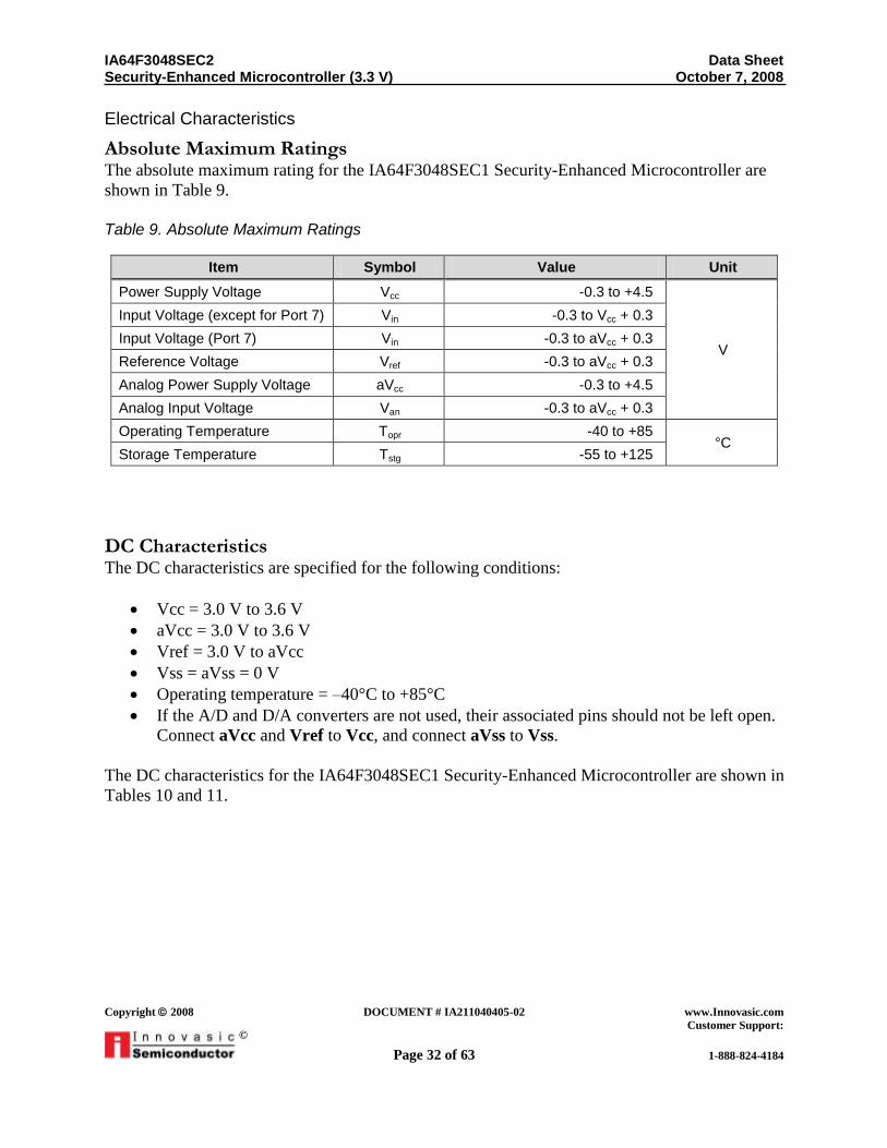
Absolute Maximum Ratings The absolute maximum rating for the IA64F3048SEC1 Security-Enhanced Microcontroller are
shown in Table 9.
Table 9. Absolute Maximum Ratings
Item Symbol Value Unit
Power Supply Voltage Vcc -0.3 to +4.5
V
Input Voltage (except for Port 7) Vin -0.3 to Vcc + 0.3
Input Voltage (Port 7) Vin -0.3 to aVcc + 0.3
Reference Voltage Vref -0.3 to aVcc + 0.3
Analog Power Supply Voltage aVcc -0.3 to +4.5
Analog Input Voltage Van -0.3 to aVcc + 0.3
Operating Temperature Topr -40 to +85 °C
Storage Temperature Tstg -55 to +125
DC Characteristics The DC characteristics are specified for the following conditions:
Vcc = 3.0 V to 3.6 V
aVcc = 3.0 V to 3.6 V
Vref = 3.0 V to aVcc
Vss = aVss = 0 V
Operating temperature = –40°C to +85°C
If the A/D and D/A converters are not used, their associated pins should not be left open.
Connect aVcc and Vref to Vcc, and connect aVss to Vss.
The DC characteristics for the IA64F3048SEC1 Security-Enhanced Microcontroller are shown in
Tables 10 and 11.
IA64F3048SEC2 Data Sheet Security-Enhanced Microcontroller (3.3 V) October 7, 2008
Copyright 2008 DOCUMENT # IA211040405-02 www.Innovasic.com
Customer Support:
Page 33 of 63 1-888-824-4184
©
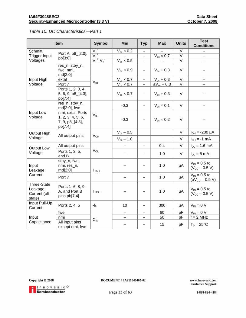
Table 10. DC Characteristics—Part 1
Item Symbol Min Typ Max Units Test
Conditions
Schmitt Trigger Input Voltages
Port A, p8_[2:0], pb[3:0]
VT- Vcc × 0.2 – – V –
VT+ – – Vcc × 0.7 V –
VT+-VT
- Vcc × 0.5 – – V –
Input High Voltage
res_n, stby_n, fwe, nmi, md[2:0]
VIH
Vcc × 0.9 – Vcc + 0.3 V –
extal Vcc × 0.7 – Vcc + 0.3 V –
Port 7 Vcc × 0.7 – aVcc + 0.3 V –
Ports 1, 2, 3, 4, 5, 6, 9, p8_[4:3], pb[7:4]
Vcc × 0.7 – Vcc + 0.3 V –
Input Low Voltage
res_n, stby_n, md[2:0], fwe
VIL
-0.3 – Vcc × 0.1 V –
nmi; extal; Ports 1, 2, 3, 4, 5, 6, 7, 9, p8_[4:3], pb[7:4]
-0.3 – Vcc × 0.2 V –
Output High Voltage
All output pins VOH Vcc – 0.5 V IOH = -200 µA
Vcc – 1.0 V IOH = -1 mA
Output Low Voltage
All output pins
VOL
– – 0.4 V IOL = 1.6 mA
Ports 1, 2, 5, and B
– – 1.0 V IOL = 5 mA
Input Leakage Current
stby_n, fwe, nmi, res_n, md[2:0] I IIN I
– – 1.0 µA VIN = 0.5 to (VCC – 0.5 V)
Port 7 – – 1.0 µA VIN = 0.5 to (aVCC – 0.5 V)
Three-State Leakage Current (off state)
Ports 1–6, 8, 9, A, and Port B pins pb[7:4]
I ITS I – – 1.0 µA VIN = 0.5 to (VCC – 0.5 V)
Input Pull-Up Current
Ports 2, 4, 5 -lP 10 – 300 µA VIN = 0 V
Input Capacitance
fwe
CIN
– – 60 pF VIN = 0 V
nmi – – 50 pF f = 2 MHz
All input pins except nmi, fwe
– – 15 pF T0 = 25°C
IA64F3048SEC2 Data Sheet Security-Enhanced Microcontroller (3.3 V) October 7, 2008
Copyright 2008 DOCUMENT # IA211040405-02 www.Innovasic.com
Customer Support:
Page 34 of 63 1-888-824-4184
©
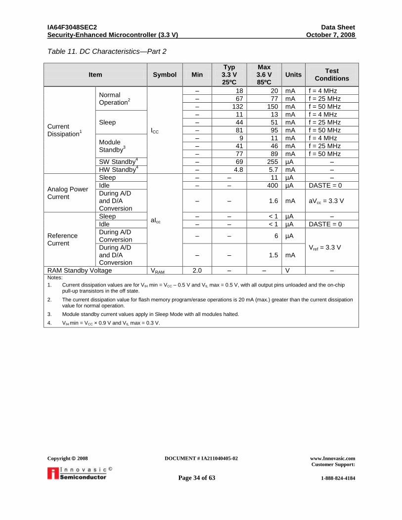
Table 11. DC Characteristics—Part 2
Item Symbol Min Typ 3.3 V 25ºC
Max 3.6 V 85ºC
Units
Test Conditions
Current Dissipation
1
Normal Operation
2
ICC
– 18 20 mA f = 4 MHz
– 67 77 mA f = 25 MHz
– 132 150 mA f = 50 MHz
Sleep
– 11 13 mA f = 4 MHz
– 44 51 mA f = 25 MHz
– 81 95 mA f = 50 MHz
Module Standby
3
– 9 11 mA f = 4 MHz
– 41 46 mA f = 25 MHz
– 77 89 mA f = 50 MHz
SW Standby4 – 69 255 µA –
HW Standby4 – 4.8 5.7 mA –
Analog Power Current
Sleep
aIcc
– – 11 µA –
Idle – – 400 µA DASTE = 0
During A/D and D/A Conversion
– – 1.6 mA aVcc = 3.3 V
Reference Current
Sleep – – < 1 µA –
Idle – – < 1 µA DASTE = 0
During A/D Conversion
– – 6 µA
Vref = 3.3 V During A/D and D/A Conversion
– – 1.5 mA
RAM Standby Voltage VRAM 2.0 – – V – Notes:
1. Current dissipation values are for VIH min = VCC – 0.5 V and VIL max = 0.5 V, with all output pins unloaded and the on-chip pull-up transistors in the off state.
2. The current dissipation value for flash memory program/erase operations is 20 mA (max.) greater than the current dissipation value for normal operation.
3. Module standby current values apply in Sleep Mode with all modules halted.
4. VIH min = VCC × 0.9 V and VIL max = 0.3 V.

IA64F3048SEC2 Data Sheet Security-Enhanced Microcontroller (3.3 V) October 7, 2008
Copyright 2008 DOCUMENT # IA211040405-02 www.Innovasic.com
Customer Support:
Page 35 of 63 1-888-824-4184
©
Permissible Output Currents
The conditions used to specify the permissible output currents are as follows:
Vcc = 3.0 V to 3.65 V
aVcc = 3.0 V to 3.6 V
Vref = 3.0 V to aVcc
Vss = aVss = 0V
Operating temperature = -40ºC to +85ºC
Permissible output currents are shown in Table 12.
Table 12. Permissible Output Currents
Item Symbol Min Typ Max Units
Permissible output Low current (per pin)
Ports 1, 2, 5, and B IOL
– – 10
mA
Other output pins – – 2.0
Permissible output Low current (total)
Total of 28 pins in Ports 1, 2, 5, and B
ΣIOL
– – 80
Total of all output pins including the above
– – 120
Permissible output High current (per pin)
All output pins IOL – – 2.0
Permissible output High current (total)
Total of all output pins
ΣIOL – – 40
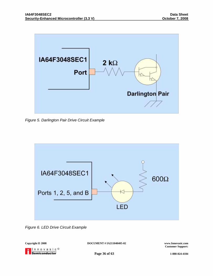
Note: To protect chip reliability, do not exceed the output current values in Table 11. When driving a Darlington pair or LED, always insert a current-limiting resistor in the output line, as shown in Figures 5 and 6.
Figure 5 shows an example Darlington-pair drive circuit, and Figure 6 shows an example of an
LED drive circuit.
IA64F3048SEC2 Data Sheet Security-Enhanced Microcontroller (3.3 V) October 7, 2008
Copyright 2008 DOCUMENT # IA211040405-02 www.Innovasic.com
Customer Support:
Page 36 of 63 1-888-824-4184
©
Figure 5. Darlington Pair Drive Circuit Example
Figure 6. LED Drive Circuit Example

IA64F3048SEC2 Data Sheet Security-Enhanced Microcontroller (3.3 V) October 7, 2008
Copyright 2008 DOCUMENT # IA211040405-02 www.Innovasic.com
Customer Support:
Page 37 of 63 1-888-824-4184
©
AC Characteristics
The conditions used to specify the AC characteristics are as follows:
Vcc = 3.0 V to 3.6 V
aVcc = 3.0 V to 3.6 V
Vref = 3.0 V to aVcc
Vss = aVss = 0V
Operating temperature = -40ºC to +85ºC
The output load circuit is shown in Figure 7.
Figure 7. Output Load Circuit
IA64F3048SEC2 Data Sheet Security-Enhanced Microcontroller (3.3 V) October 7, 2008
Copyright 2008 DOCUMENT # IA211040405-02 www.Innovasic.com
Customer Support:
Page 38 of 63 1-888-824-4184
©
The AC characteristics are presented in the following tables and figures:
Bus Timing Table 13 (parameters)
Figures 8–10 (waveforms)
Refresh Controller Bus Timing Table 14 (parameters)
Figures 11–18 (waveforms)
Clock and Control Signal Timing Table 15 (parameters)
Figures 19–22 (waveforms)
On-Chip System Module Timing Table 16 (parameters)
Figures 23–30 (waveforms)

IA64F3048SEC2 Data Sheet Security-Enhanced Microcontroller (3.3 V) October 7, 2008
Copyright 2008 DOCUMENT # IA211040405-02 www.Innovasic.com
Customer Support:
Page 39 of 63 1-888-824-4184
©
Table 13. Bus Timing Parameters
Item Symbol Min Max Unit
Clock cycle time tCYC 20 250
ns
Clock pulse low width tCL 10 —
Clock pulse high width tCH 10 —
Clock rise time tCR — 10
Clock fall time tCF — 10
Address delay time tAD — 30
Address hold time tAH 0.5tCYC − 20 —
Address strobe delay time tASD — 25
Write strobe delay time tWSD — 25
Strobe delay time tSD — 25
Write data strobe pulse width 1 tWSW1 1.0tCYC − 25 —
Write data strobe pulse width 2 tWSW2 1.5tCYC – 25 —
Address setup time 1 tAS1 0.5tCYC – 25 —
Address setup time 2 tAS2 1.0tCYC – 25 —
Read data setup time tRDS 20 —
Read data hold time tRDH 0 —
Write data delay time tWDD — 40
Write data setup time 1 tWDS1 1.0tCYC – 35 —
Write data setup time 2 tWDS2 0.5tCYC – 35 —
Write data hold time tWDH 0.5tCYC – 15 —
Read data access time 1 tACC1 — 1.5tCYC – 50
Read data access time 2 tACC2 — 2.5tCYC – 50
Read data access time 3 tACC3 — 1.0tCYC – 45
Read data access time 4 tACC4 — 2.0tCYC – 45
Precharge time tPCH 1.0tCYC – 20 —
Wait setup time tWTS 25 —
Wait hold time tWTH 5 —
Bus request setup time tBRQS 25 —
Bus acknowledge delay time 1 tBACD1 — 30
Bus acknowledge delay time 2 tBACD2 — 30
Bus-floating time tBZD — 40

IA64F3048SEC2 Data Sheet Security-Enhanced Microcontroller (3.3 V) October 7, 2008
Copyright 2008 DOCUMENT # IA211040405-02 www.Innovasic.com
Customer Support:
Page 40 of 63 1-888-824-4184
©
Figure 8. Basic Bus Cycle, Two-State Access
IA64F3048SEC2 Data Sheet Security-Enhanced Microcontroller (3.3 V) October 7, 2008
Copyright 2008 DOCUMENT # IA211040405-02 www.Innovasic.com
Customer Support:
Page 41 of 63 1-888-824-4184
©
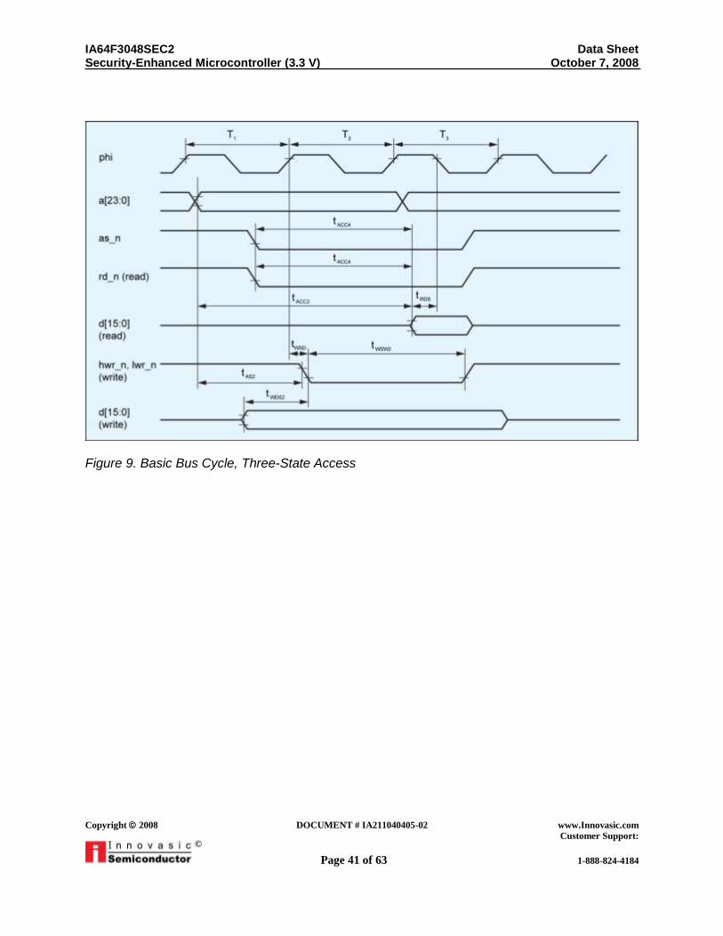
Figure 9. Basic Bus Cycle, Three-State Access

IA64F3048SEC2 Data Sheet Security-Enhanced Microcontroller (3.3 V) October 7, 2008
Copyright 2008 DOCUMENT # IA211040405-02 www.Innovasic.com
Customer Support:
Page 42 of 63 1-888-824-4184
©
Figure 10. Basic Bus Cycle, Three-State Access with One Wait State
IA64F3048SEC2 Data Sheet Security-Enhanced Microcontroller (3.3 V) October 7, 2008
Copyright 2008 DOCUMENT # IA211040405-02 www.Innovasic.com
Customer Support:
Page 43 of 63 1-888-824-4184
©
Table 14. Refresh Controller Timing Parameters
Item Symbol Min Max Unit
ras_n delay time 1 tRAD1 — 30
ns
ras_n delay time 2 tRAD2 — 30
ras_n delay time 3 tRAD3 — 30
Row address hold time tRAH 0.5tCYC − 5 —
ras_n precharge time tRP 1.0tCYC – 15 —
cas_n to ras_n precharge time tCRP 1.0tCYC – 15 —
cas_n pulse width tCAS 1.0tCYC – 18 —
ras_n access time tRAC — 2.0tCYC – 35
Address access time tAA — 1.5tCYC – 40
cas_n access time tCAC — 1.0tCYC – 30
Write data setup time 3 tWDS3 15 —
cas_n setup time tCSR 0.5tCYC – 15 —
Read strobe delay time tRSD — 25

IA64F3048SEC2 Data Sheet Security-Enhanced Microcontroller (3.3 V) October 7, 2008
Copyright 2008 DOCUMENT # IA211040405-02 www.Innovasic.com
Customer Support:
Page 44 of 63 1-888-824-4184
©
Figure 11. DRAM Bus Timing, Read/Write, Three-State Access, 2we_n Mode

IA64F3048SEC2 Data Sheet Security-Enhanced Microcontroller (3.3 V) October 7, 2008
Copyright 2008 DOCUMENT # IA211040405-02 www.Innovasic.com
Customer Support:
Page 45 of 63 1-888-824-4184
©
Figure 12. DRAM Bus Timing, Refresh Cycle, Three-State Access, 2we_n Mode

IA64F3048SEC2 Data Sheet Security-Enhanced Microcontroller (3.3 V) October 7, 2008
Copyright 2008 DOCUMENT # IA211040405-02 www.Innovasic.com
Customer Support:
Page 46 of 63 1-888-824-4184
©
Figure 13. DRAM Bus Timing, Self-Refresh Mode, 2we_n Mode

IA64F3048SEC2 Data Sheet Security-Enhanced Microcontroller (3.3 V) October 7, 2008
Copyright 2008 DOCUMENT # IA211040405-02 www.Innovasic.com
Customer Support:
Page 47 of 63 1-888-824-4184
©
Figure 14. DRAM Bus Timing, Read/Write, Three-State Access, 2cas_n Mode

IA64F3048SEC2 Data Sheet Security-Enhanced Microcontroller (3.3 V) October 7, 2008
Copyright 2008 DOCUMENT # IA211040405-02 www.Innovasic.com
Customer Support:
Page 48 of 63 1-888-824-4184
©
Figure 15. DRAM Bus Timing, Refresh Cycle, Three-State Access, 2cas_n Mode

IA64F3048SEC2 Data Sheet Security-Enhanced Microcontroller (3.3 V) October 7, 2008
Copyright 2008 DOCUMENT # IA211040405-02 www.Innovasic.com
Customer Support:
Page 49 of 63 1-888-824-4184
©
Figure 16. DRAM Bus Timing, Self-Refresh Mode, 2we_n Mode

IA64F3048SEC2 Data Sheet Security-Enhanced Microcontroller (3.3 V) October 7, 2008
Copyright 2008 DOCUMENT # IA211040405-02 www.Innovasic.com
Customer Support:
Page 50 of 63 1-888-824-4184
©
Figure 17. PSRAM Bus Timing, Read/Write, Three-State Access

IA64F3048SEC2 Data Sheet Security-Enhanced Microcontroller (3.3 V) October 7, 2008
Copyright 2008 DOCUMENT # IA211040405-02 www.Innovasic.com
Customer Support:
Page 51 of 63 1-888-824-4184
©
Figure 18. PSRAM Bus, Refresh Cycle

IA64F3048SEC2 Data Sheet Security-Enhanced Microcontroller (3.3 V) October 7, 2008
Copyright 2008 DOCUMENT # IA211040405-02 www.Innovasic.com
Customer Support:
Page 52 of 63 1-888-824-4184
©
Table 15. Refresh Controller Timing Parameters
Item Symbol Min Max Unit
res_n setup tRESS 150 — ns
res_n pulse time tRESW 20 — tCYC
Mode programming setup time tMDS 200 —
ns
NMI setup time (nmi, irq[5:0]_n) tNMIS 150 —
NMI hold time (nmi, irq[5:0]_n) tNMIH 10 —
Interrupt pulse width (nmi, irq[2:0]_n when exiting Software Standby Mode)
tNMIW 200 —
Clock oscillator settling time at rest (crystal) tOSC1 20 —
ms Clock oscillator settling time in Software Standby Model (crystal)
tOSC2 7 —
Figure 19. Oscillator Settling Time

IA64F3048SEC2 Data Sheet Security-Enhanced Microcontroller (3.3 V) October 7, 2008
Copyright 2008 DOCUMENT # IA211040405-02 www.Innovasic.com
Customer Support:
Page 53 of 63 1-888-824-4184
©
Figure 20. Reset Input Timing
Figure 21. Interrupt Input Timing

IA64F3048SEC2 Data Sheet Security-Enhanced Microcontroller (3.3 V) October 7, 2008
Copyright 2008 DOCUMENT # IA211040405-02 www.Innovasic.com
Customer Support:
Page 54 of 63 1-888-824-4184
©
Figure 22. Bus-Release Mode Timing

IA64F3048SEC2 Data Sheet Security-Enhanced Microcontroller (3.3 V) October 7, 2008
Copyright 2008 DOCUMENT # IA211040405-02 www.Innovasic.com
Customer Support:
Page 55 of 63 1-888-824-4184
©
Table 16. On-Chip System Module Timing Parameters
Item Symbol Min Max Unit
DMAC
dreq_n setup time tDRQS 20 —
ns
dreq_n hold time tDRQH 10 —
tend_n delay time 1 tTED1 — 50
tend_n delay time 2 tTED2 — 50
ITU
Timer output delay time tTOCD — 50
Time input setup time tTICS 40 —
Timer clock input setup time tTCKS 40 —
Timer clock pulse width
Single edge tTCKWH 1.5 —
tCYC
Both edges tTCKWL 2.5 —
SCI
Input clock cycle Asychronous tSCYC 4 tCYC
Synchronous tSCYC 6 tCYC
Input clock rise time tSCKr — 1.5
Input clock fall time tSCKt — 1.5
Input clock pulse width tSCKW 0.4 0.6 tSCYC
SCI
Transmit data delay time tTXD — 100
ns
Receive data setup time (synchronous) tRXS 100 —
Receive data hold time (synchronous)
Clock input tRXH 100 —
Clock output tRXH 0 –
Ports and TPC
Output data delay time tPWD — 50
Input data setup time tPRS 50 —
Input data hold time tPRH 50 —

IA64F3048SEC2 Data Sheet Security-Enhanced Microcontroller (3.3 V) October 7, 2008
Copyright 2008 DOCUMENT # IA211040405-02 www.Innovasic.com
Customer Support:
Page 56 of 63 1-888-824-4184
©
Figure 23. Direct Memory Access Controller (DMAC) dreq_n Input Timing
Figure 24. DMAC tend_n Output Timing, Two-State Access
IA64F3048SEC2 Data Sheet Security-Enhanced Microcontroller (3.3 V) October 7, 2008
Copyright 2008 DOCUMENT # IA211040405-02 www.Innovasic.com
Customer Support:
Page 57 of 63 1-888-824-4184
©
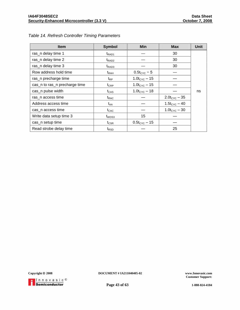
Figure 25. DMAC tend_n Output Timing, Three-State Access
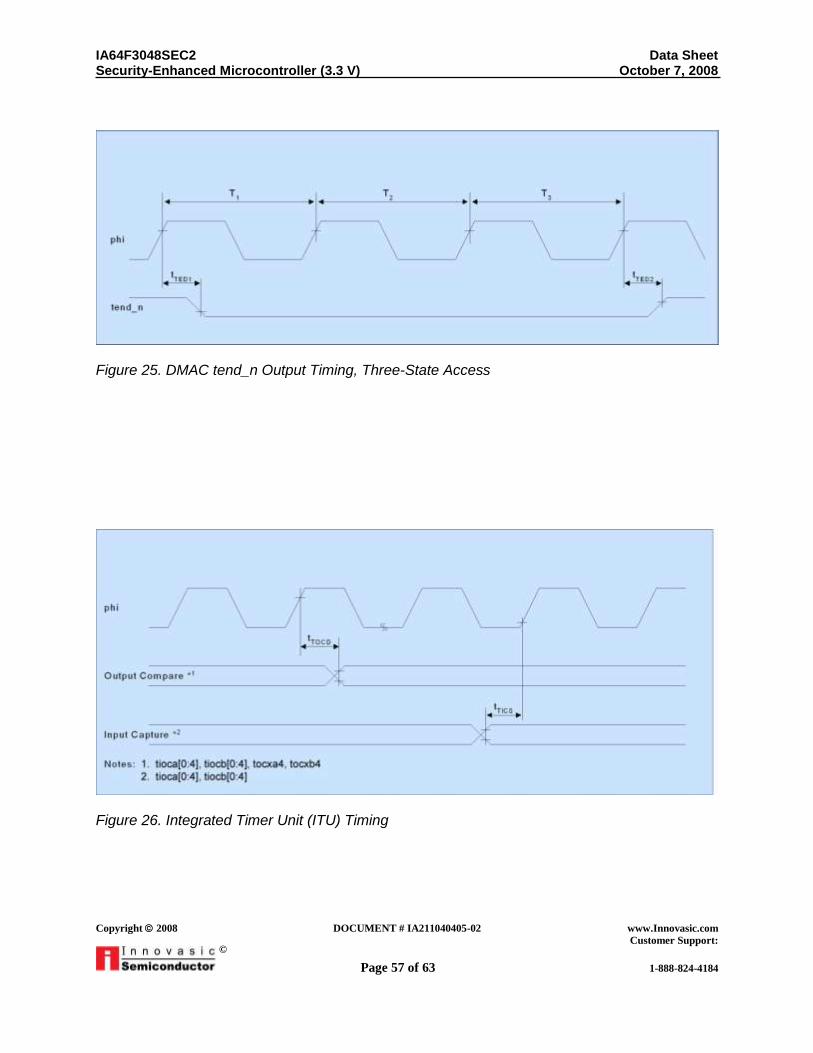
Figure 26. Integrated Timer Unit (ITU) Timing

IA64F3048SEC2 Data Sheet Security-Enhanced Microcontroller (3.3 V) October 7, 2008
Copyright 2008 DOCUMENT # IA211040405-02 www.Innovasic.com
Customer Support:
Page 58 of 63 1-888-824-4184
©
Figure 27. ITU External Clock Input Timing
Figure 28. Serial Communication Interface (SCI) sck Input Clock Timing

IA64F3048SEC2 Data Sheet Security-Enhanced Microcontroller (3.3 V) October 7, 2008
Copyright 2008 DOCUMENT # IA211040405-02 www.Innovasic.com
Customer Support:
Page 59 of 63 1-888-824-4184
©
Figure 29. SCI Input/Output Timing, Synchronous Mode
Figure 30. SCI Timing Pattern Controller (TPC) and I/O Port Timing

IA64F3048SEC2 Data Sheet Security-Enhanced Microcontroller (3.3 V) October 7, 2008
Copyright 2008 DOCUMENT # IA211040405-02 www.Innovasic.com
Customer Support:
Page 60 of 63 1-888-824-4184
©
Physical Dimensions The physical dimensions for the IA64F3048SEC1 100-lead Thin Quad Flat Package (TQFP) are
shown in Figure 31 and Table 17.
Figure 31. IA64F3048SEC1 100-Lead TQFP Physical Dimensions

IA64F3048SEC2 Data Sheet Security-Enhanced Microcontroller (3.3 V) October 7, 2008
Copyright 2008 DOCUMENT # IA211040405-02 www.Innovasic.com
Customer Support:
Page 61 of 63 1-888-824-4184
©
Table 17. IA64F3048SEC1 100-Lead TQFP Physical Dimensions
Dimension Minimum Nominal Maximum Units
Number of Pins N — 100 — —
Pins per Side — — 25 — —
Pitch e — 0.5 —
Millimeters
(mm)
Overall Height A — — 1.20
Molded Package Thickness A2 0.95 1.00 1.05
Standoff A1 0.05 — 0.15
Foot Length L 0.45 0.6 0.75
Footprint (Reference) L1 — 1.0 —
Overall Width D — 16.0 16.4
Overall Length E — 16.0 16.4
Molded Package Width D1 — 14.0 14.1
Molded Package Length E1 — 14.0 14.1
Lead Thickness c — 0.08 0.20
Lead Width b 0.17 0.20 0.27
Mold Draft Angle Top 11 12 13 Degrees
(°) Mold Draft Angle Bottom 11 12 13
Foot Angle 0 3.5 7

IA64F3048SEC2 Data Sheet Security-Enhanced Microcontroller (3.3 V) October 7, 2008
Copyright 2008 DOCUMENT # IA211040405-02 www.Innovasic.com
Customer Support:
Page 62 of 63 1-888-824-4184
©
Ordering Information The IA64F3048SEC1 is currently available in the package styles listed in and Table 18.
Table 18. IA64F3048SEC1 Ordering Information
Package Style Temperature Grade Order Number
100-Lead Thin Quad Flat
Package (TQFP), 1-mm
Package
Industrial IA64F3048SEC1TQFP100
Other package styles and temperature grades may be available at an additional cost, with
additional lead times, or both.
Innovasic Semiconductor, Inc. Office: 505.883.5263 3737 Princeton Drive NE, Suite 130 FAX: 505.883.5477 Albuquerque, NM 87107-4237 Toll Free: 1-888.824.4184
www.innovasic.com

IA64F3048SEC2 Data Sheet Security-Enhanced Microcontroller (3.3 V) October 7, 2008
Copyright 2008 DOCUMENT # IA211040405-02 www.Innovasic.com
Customer Support:
Page 63 of 63 1-888-824-4184
©
Errata
Version -05 Errata (as of October 2007):
Problem: The second page of a two-page S-record gets programmed to the location of the first
page when the first page contains all blanks.
Analysis: When an S-record spans two pages and the first of those pages contains all blanks, the
second page gets programmed at the location of the first page. This will not occur if the first
page is in base space and second page is in field space and the base space security bit is set so
there are no security implications.
Workaround: Change the boot mode loading software running on the PC to split S-records that
begin with either 00h or ffh up to the page boundary.