hydrogen diffusion and ion implantation in silicon carbide ...9286/fulltext01.pdf · janson, m.s.,...
TRANSCRIPT

Hydrogen diffusion and ion implantation
in silicon carbide
Martin Janson
KTH, Royal Institute of TechnologyMaterials and Semiconductor PhysicsStockholm 2003


Hydrogen diffusion and ion implantationin silicon carbide
Martin Janson
Materials and Semiconductor PhysicsStockholm 2003

The graph at the top of the cover shows the Si (○) and C (●)atoms of the Si terminated (0001) surface of 4H-SiC.
Hydrogen diffusion and ion implantationin silicon carbide
A dissertation submitted to Kungliga Tekniska Högskolan,Stockholm, Sweden, in partial fulfillment of the requirements for thedegree of teknologie doktor.
© 2003 Martin JansonKTH, Royal Institute of TechnologyDepartment of Microelectronics and Information TechnologyMaterials and Semiconductor Physics LaboratoryElectrum 229SE-164 40Sweden
ISRN KTH/FTE/FR-2003/2-SEISSN 0284-0545TRITA-FTEForskningsrapport 2003:2
Printed in 250 copies by Universitetsservice US AB, Stockholm 2003

Janson, M.S., Hydrogen diffusion and ion implantation in silicon carbideISRN KTH/FTE/FR-2003/2-SE, ISSN 0284-0545KTH, Royal Institute of Technology, Department of Microelectronics and Information TechnologyStockholm 2003
AbstractSecondary ion mass spectrometry (SIMS) has been employed to study the spatialdistributions resulting from mass transport by diffusion and ion implantation insingle crystal silicon carbide (SiC). By a systematic analysis of this data,fundamental processes that govern these phenomena have been derived.
The acceptor atoms Al and B are known to be electrically passivated by H in SiC.By studying the thermally stimulated redistribution of implanted deuterium (2H) invarious acceptor doped structures, it is found that hydrogen forms complexeswith the doping atoms, and also interacts strongly with implantation induceddefects. A comprehensive understanding of the formation and dissociationkinetics of these complexes has been obtained. The extracted effective captureradius for the formation of 2H-B complexes is in good agreement with thatexpected for a coulomb force assisted trapping mechanism. The large differenceof 0.9 eV in the extracted dissociation energies for the 2H-Al and 2H-B complexessuggests that the atomic configurations of the two complexes are significantlydifferent. Furthermore, by studying the migration behavior of H in the presenceof built-in electric fields, it is concluded that all of the mobile H is in the positivecharge state in p-type SiC.
A large number of implantations have been performed with respect to ion mass,energy, fluence, and crystal orientation. The electronic stopping cross sections inthe low velocity regime for ions with atomic numbers 1 ≤ Z1 ≤ 15 have beenextracted from the ion range distributions. They display both Z1-oscillations and asmaller than velocity proportional stopping for ions with Z1 ≤ 8, in agreementwith previous reports for other materials. Furthermore, the degree of ionchanneling in various major axial and planar channels of the 6H and 4H-SiCcrystal has been explored. Two types of ion implantation simulators have beendeveloped. One based on a statistical, data-base approach, and one atomisticsimulator, based on the binary collision approximation (BCA). By fitting BCAsimulated profiles to the experimental profiles, detailed information about theelectronic stopping and implantation induced damage is extracted. In addition, thevacancy-related damage caused by the implantations has been investigated bypositron annihilation spectroscopy (PAS). Two types of implantation inducedpositron traps have been isolated and are tentatively identified as a Si vacancy(VSi) and a Si-C divacancy (VSiVC). The extension of detected VSi is in goodagreement with that predicted by BCA simulations, and for implantations withheavier ions VSi are revealed at far greater depths than the mean projected ionrange due to deeply penetrating channeled ions.


i
Contents
List of appended papers iiPublished work not appended iii
Author’s contribution to appended papers vii
Abbreviations viii
1 Introduction 1
2 Silicon carbide2.1 Crystal structure and fundamental properties 52.2 Doping 10
3 Measurement techniques3.1 Secondary ion mass spectrometry 123.2 Positron annihilation spectroscopy 23
4 Hydrogen migration and complex formation insemiconductors 434.1 Hydrogen–acceptor complex 444.2 Migration of hydrogen 54
5 Ion implantation: range and damage distributions 605.1 Stopping power 615.2 Ion channeling 685.3 Implantation induced damage 745.4 Simulation of ion implantation 78
6 Summary of results 90
Acknowledgements 93
Appendix A Solution of the positron transport equation at steady state 95 B Steady-state H profiles in the presence of doping gradients
and trapping 98 C Quasi random number algorithm for the thermal
vibration model 100
References 101

ii
Appended papers
I. Hydrogen diffusion, complex formation and dissociation in acceptor dopedsilicon carbideM. S. Janson, M. K. Linnarsson, A. Hallén and B. G. SvenssonPhys. Rev. B 64, 195202/1-12 (2001)
II. Electric field assisted migration and accumulation of hydrogen in siliconcarbideM. S. Janson, M. K. Linnarsson, A. Hallén, B. G. Svensson, N. Nordell andS. KarlssonPhys. Rev. B 61(11), 7195-7198 (2000)
III. Hydrogen-boron complex formation and dissociation in 4H- silicon carbideM. S. Janson, M. K. Linnarsson, A. Hallén and B. G. SvenssonAppl. Surf. Sci. 184, 257-262 (2001)
IV. Dissociation of deuterium-defect complexes in ion-implanted epitaxial 4H-SiCM. Janson, M. K. Linnarsson, A. Hallén and B. G. SvenssonMater. Res. Soc. Symp. 513, 439-444 (1998)
V. Electronic stopping cross sections in silicon carbide for low-velocity ionswith 1 ≤ Z1 ≤ 15M. S. Janson, M. K. Linnarsson, A. Hallén and B. G. SvenssonSubmitted to Phys. Rev. B (Nov. 2002)
VI. Channeled implants in 6H silicon carbideM. S. Janson, A. Hallén, P. Godignon, A. Y. Kuznetsov, M. K. Linnarsson,E. Morwan and B. G. SvenssonMater. Sci. Forum 338-342, 889-892 (2000)
VII. Effect of crystal orientation and direction on the implant profile of 60 keV Alinto 4H-SiC crystalsJ. Wong-Leung, M. S. Janson and B. G. SvenssonSubmitted to J. Appl. Phys. (Feb. 2003)
VIII. Ion implantation range distributions in silicon carbideM. S. Janson, M. K. Linnarsson, A. Hallén and B. G. SvenssonSubmitted to J. Appl. Phys. (Nov. 2002)
IX. Vacancy type defect distributions of 11B-, 14N-, and 27Al-implanted 4H-SiCstudied by positron annihilation spectroscopyM. S. Janson, J. Slotte, A. Y. Kuznetsov, K. Saarinen and A. HallénMater. Sci. Forum (2003), in press

iii
Published work not appended
First authorTransient enhanced diffusion of implanted boron in 4H-silicon carbideM. S. Janson, M. K. Linnarsson, A. Hallén, B. G. Svensson, N. Nordell and H. BleichnerAppl. Phys. Lett. 76(11), 1434-1436 (2000)
Dissociation Energy of the passivating hydrogen-aluminum complex in 4H siliconcarbideM. S. Janson, A. Hallén, M. K. Linnarsson, N. Nordell, S. Karlsson and B. G. SvenssonMater. Sci. Forum 353-356, 427-430 (2001)
Diffusion of dopants and impurities in device structures of SiC, SiGe and SiM. S. Janson, M. K. Linnarsson, J. S. Christensen, P. Leveque, A. Y. Kuznetsov,H. H. Radamson, A. Hallén, A. Nylandsted-Larsen and B. G. SvenssonDefect and Diffusion Forum 194-199, 597-610 (2001)
Range distributions of implanted ions in silicon carbideM. S. Janson, M. K. Linnarsson, A. Hallén and B. G. SvenssonMater. Sci. Forum 389-393, 779-792 (2002)
The role of channeling for deep vacancy distributions in ion implanted 4H-SiCM. S. Janson, J. Slotte, A. Y. Kuznetsov, K. Saarinen and A. HallénSubmitted to J. Appl. Phys. (Feb. 2003)
Co-authorHydrogen passivation of silicon carbide by low-energy ion implantationN. Achtziger, J. Grillenberger, W. Witthuhn, M. K. Linnarsson, M. Janson andB. G. SvenssonAppl. Phys. Lett. 73(7), 945-947 (1998)
Mobility, Passivating Effects and Thermal Stability of Hydrogen in Silicon CarbideN. Achtziger, C.Hülsen, W. Witthuhn, M. K. Linnarsson, M. Janson and B. G. SvenssonPhys. Stat. Sol (b) 210(395), 395-399 (1998)
Deuterium incorporation in acceptor-doped epitaxial layers of 6H-SiCM. K. Linnarsson, M. Janson, A. Schöner, N. Nordell, S. Karlsson and B. G. SvenssonMater. Sci. Forum 264-268, 761-764 (1998)
Boron diffusion in Si and SiC during 2.5 MeV proton irradiation at 500-850 °CA. Y. Kuznetsov, M. Janson, A. Hallén, B. G. Svensson and A. Nylandsted LarsenNucl. Instr. Meth. Phys. Res. B 148, 279-283 (1999)
iv
Diffusion of light elements in 4H- and 6H-SiCM. K. Linnarsson, M. Janson, S. Karlsson, A. Schöner, N. Nordell and B. G. SvenssonMater. Sci. and Eng. B 61-62, 275-280 (1999)
Metal-contact enhanced incorporation of deuterium in 4H- and 6H-silicon carbideM. K. Linnarsson, A. Lloyd. Spetz, M. S. Janson, L. G. Ekdahl, S. Karlsson, A. Schöner,I. Lundström and B. G. SvenssonMater. Sci. Forum 338-342, 937-940 (2000)
Formation of passivated layers in p-type SiC by low energy ion implantation ofhydrogenN. Achtziger, C. Hülsen, M. S. Janson, M.K. Linnarsson, B. G. Svensson and W. WitthuhnMater. Sci. Forum 338-342, 933-936 (2000)
Atomistic simulation of ion implantation into different polytypes of SiCA. Ster, M. Posselt, A. Hallén and M. Jansonin Proceedings of Inter. Conf. on Ion Implantation Tech. 2000 (IEEE, 2000), 220-223
Demonstration of Lateral Boron Diffusion in 4H-SiC Using the JBS device as teststructureF. Dahlquist, H. Lendemann, M. S. Janson and B. G. SvenssonJ. Future Electron Devices 11(2), 60-62 (2000)
Characterisation of ion-implantation-induced defects in Silicon CarbideD. Åberg, P. O. Å. Persson, E. Morvan, M. K. Linnarsson, A. Y. Kuznetsov, A. Hallén,M. S. Janson, L. Hultman and B. G. Svensson1st International Workshop on Ultra-Low-Loss Power Device TechnologyUPD2000, Nara-Japan; extended abstract
Doping of Silicon Carbide by Ion ImplantationB. G. Svensson, A. Hallén, M. K. Linnarsson, A. Y. Kuznetsov, M. S. Janson, D. Åberg,J. Österman, P. O. Å. Persson, L. Hultman, L. Storasta, F. C. H. Carlsson, J. P. Bergman,C. Jagadish and E. MorvanMater. Sci. Forum 353-356, 594-554 (2001)
Channeling measurements of ion implantation damage in 4H-SiCA. Y. Kuznetsov, M. S. Janson, A. Hallén, B. G. Svensson, C. Jagadish, H. Grünleitner andG. PenslMater. Sci. Forum 353-356, 595-598 (2001)
Solubility limit and precipitate formation in Al-doped 4H-SiC epitaxial materialM. K. Linnarsson, M. S. Janson, U. Zimmermann, B. G. Svensson, P. O. Å. Persson,L. Hultman, J. Wong-Leung, S. Karlsson, A. Schöner, H. Bleichner and E. OlssonAppl. Phys. Lett. 79(13), 2016-2018 (2001)

v
Precipitate formation in heavily Al-doped 4H-SiC layersM. K. Linnarsson, P. O. Å. Persson, H. Bleichner, M. S. Janson, U. Zimmermann,H. Andersson, S. Karlsson, R. Yakimova, L. Hultman and B. G. SvenssonMater. Sci. Forum 353-356, 583-586 (2001)
Incorporation of Hydrogen (1H and 2H) in 4H-SiC during epitaxial growthM. K. Linnarsson, U. Forsberg, M. S. Janson, E. Janzén and B. G. SvenssonMater. Sci. Forum 389-393, 565-568 (2002)
The effect of hydrogen diffusion in p- and n-type SiC Scottky diodes at hightemperatureL. Unéus, S. Nakagomi, M. K. Linnarsson, M. S. Janson, B. G. Svensson, R. Yakimova,M. Syväjärvi, A. Henry, E. Janzén, L. G. Ekdahl, I. Lundström and A. Lloyd SpetzMater. Sci. Forum 389-393, 1419-1422 (2002)
On the nature of ion implantation induced dislocation loops in 4H-silicon carbideP. O. Å. Persson, L. Hultman, M. S. Janson, A. Hallén, R. Yakimova, D. Panknin andW. SkorupaJ. Appl. Phys 92(5), 2501-2505 (2002)
Ion implantation of silicon carbideA. Hallén, M. S. Janson, A. Y. Kuznetsov, D. Åberg, M. K. Linnarsson, B. G. Svensson,P. O. Å. Persson, F. H. C. Carlsson, L. Storasta, J. P. Bergman, S. G. Sridhara andY. ZhangNucl. Instr. Meth. Phys. Res. B 186, 186-194 (2002)
Solubility limits of dopants in 4H-SiCM. K. Linnarsson, U. Zimmermann, J. Wong-Leung, A. Schöner, M. S. Janson, C. Jagadishand B. G. SvenssonAppl. Surf. Sci. 203-204, 427-432 (2003)
Scanning Spreading Resistance Microscopy of Aluminum Implanted 4H-SiCJ. Osterman, L. Abtin, U. Zimmermann, M. S. Janson, S. Anand, C. Hallin and A. HallénMater. Sci. Eng. B., in press
Formation of pn-junctions in deep silicon pores for X-ray imaging detectorapplicationsX. Badel, J. Linnros, M. S. Janson and J. ÖstermanNucl. Instr. Meth. Phys. Res. A, (accepted 2003)
Disorder Profile and Annealing Behavior in Al-implanted 4H-SiCY. Zhang, W. J. Weber, W. Jiang, M. S. Janson, A. Hallén, V. Shuttanandan,S. Thevuthasan and G. PossnertSubmitted to J. Mater. Res., (2002)
Dislocation loop evolution in Ion Implanted 4H-SiCP. O. Å. Persson, L. Hultman, M. S. Janson, A. Hallén and R. YakimovaSubmitted to J. Appl. Phys., (Dec. 2002)

vi
The nature of the 3838Å-photoluminescence line in 4H-SiCA. Henry, U. Forsberg, M. S. Janson and E. JanzénSubmitted to J. Appl. Phys. (Dec. 2002)
Implanted p+n-junction in silicon carbideA. Hallén, M. S. Janson, J. Osterman, U. Zimmermann, M. K. Linnarsson, A. Y. Kuznetsov,Y. Zhang, P. O. Å. Persson and B. G. SvenssonSubmitted to 17th International Conference on the Application of Accelerators inResearch and Industry, Nov. 2002
Aluminum and boron diffusion in 4H-SiCM. K. Linnarsson, M. S. Janson, A. Schöner and B. G. SvenssonMater. Res. Soc. Proc. 742, MRS fall meeting in Boston Dec. 2002, (accepted)

vii
Author’s contribution to appended papers
I – IV. Planning, sample preparation (except for epitaxial growth and 2H-implantation), SIMS measurements, data analysis, computersimulations, and writing of the manuscript.
V, VIII. Planning, part of the SIMS measurements (~20%), data analysis,computer simulations, and writing of the manuscript.
VI. SIMS measurements and writing of the manuscript.
VII. Part of the planning (~50%), SIMS measurements, computersimulations, and part of the writing of the manuscript.
IX. Planning, coordination of sample preparation, part of the PASmeasurements, SIMS measurements, data analysis, computersimulations, and writing of the manuscript.

viii
Abbreviations
AcronymsBC Bond centered configurationBCA Binary collision approximationc-RBS Rutherford backscattering spectroscopy in the channeling
mode.CV Capacitance versus voltage measurementsDOBS Doppler-broadening spectroscopyLVM Local vibrational mode measurementsMARLOWE Implantation simulation code for crystalline targetsMD Molecular dynamics simulation algorithmMC Monte-Carlo simulation algorithmPAS Positron annihilation spectroscopySIIMPL Implantation simulation code for crystalline targets,
developed as a part of this thesisSIMS Secondary ion mass spectrometrySPB Slow positron beam techniqueTRIM Implantation simulation code for amorphous targets1D One dimensional2D Two dimensional3D Three dimensional
Symbols and constantsC ConcentrationD Diffusion constante Elementary chargeEdisp Displacement energyEd Dissociation energyEm Migration energy barrierEg Electronic energy band gapEb Binding energyE0 Ion implantation energyF Particle fluxkB Bolzmann constantL Diffusion length

ix
M1 Atomic mass number of implanted ion, scattered particleM2 Atomic mass number of target, recoiling atomp Impact parameter or energy dependence of Se, depending
on the contextT Absolute temperature or energy transferred to the recoiling
atom in a binary collision, depending on the contextR Path length of implanted particleRp Projected range of implanted particleS Annihilation line-shape parameter, centralSe Electronic (in-elastic) stopping cross sectionSn Nuclear (elastic) stopping cross sectionSnZBL Universal nuclear stopping cross section of Ziegler,
Biersack, and Littmark [102]<ux> 1D mean amplitude of thermal vibrationsVC Carbon vacancyVSi Silicon vacancyW Annihilation line-shape parameter, wingZ1 Atomic number of implanted ion, scattered particleZ2 Atomic number of target, recoiling atom
∆Ee Electronic energy loss in a binary collisionε Dielectric constantε0 Permittivity of free space.εr Relative dielectric constantη Annihilation fractionθD Debye temperatureκ Positron trapping rateλ Jump distance between neighboring lattice sitesµ Mobilityν Dissociation frequencyν0 Dissociation frequency pre-factorνlattice Characteristic vibration frequency of the latticeρ Mass densityτ Positron lifetimeτb Positron lifetime of undamaged bulk material

Hydrogen diffusion and ion implantation in silicon carbide
1
1 Introduction
Silicon carbide (SiC) is a binary compound whose extraordinary thermal,mechanical and electrical properties makes it the favored material for a widerange of application areas. Excluding its presence in some meteorites thereare no (earthly) natural sources for SiC, but it has been synthesized on anindustrial level for more than 100 years [1]. Single crystalline SiC wafersbecame commercially available about 15 years ago, a fact that dramaticallyincreased the scientific and industrial interest for SiC as an electronicmaterial.
SiC is very hard and wear resistant and has − under the name carborundum− been used as an abrasive substance ever since it was first available (e.g. inblack sand paper). The combination of extremely high thermal conductivityand thermal stability makes SiC a suitable coating material in various hightemperature applications. With the additional property of being a low-Zsubstance, SiC is further a competitive candidate as a first wall material infusion plasma devices [2]. The above mentioned properties also make SiCvery suitable for micro-fabricated sensor and actuator applications − alsoknown as microelectromechanical systems (MEMS) − intended to functionat high temperatures and in highly corrosive or erosive environments [3].
Single crystalline silicon carbide is also a wide band gap semiconductor thatcan be utilized for electronic and optical applications, as well. A lightemitting diode (LED) in SiC was demonstrated already in 1907 [4], and blueLEDs were for a long time considered to be a major market for SiC. Theefficiency for these devices is, unfortunately, rather low since SiC has anindirect band gap. The fundamental material advantages of SiC are insteadbetter utilized in electronic applications dealing with high powers, highfrequencies, and high temperatures. High power electronics, such asswitches and rectifiers used for electronic power regulation, benefit fromthe exceptional high electric breakdown field and the high thermalconductivity. This will lead to substantially smaller losses in electronicpower systems and make costly cooling redundant. Someone has estimatedthat the full realization of SiC in the power transmission and distribution
1. Introduction
2
infrastructure would save an amount of energy comparable to the capacityof one nuclear power plant in Sweden alone. Furthermore, the saturationvelocity for holes and electrons is also very high in SiC, which makes itinteresting for RF and microwave transistors. Due to the broad band gap alltypes of SiC devices could function at high temperatures and this opensnew application areas for semiconductor sensors. Examples of this includefast gas sensors operating inside car engines to give greater combustionefficiency and thereby lowering the pollution, and sensors in the heads ofdrilling equipment. A wide band gap is also favorable for low-noise UV-detectors and commercial SiC UV-detectors are now available.
This thesis deals with fundamental properties of single crystal SiC occurringat an atomic level during processing of the material. The work may bedivided into two areas: (a) Hydrogen migration and its interaction withacceptor doping atoms and implantation induced defects. (b) Ionimplantation, with an emphasis on properties related to the rangedistributions of implanted ions and vacancy related implantation induceddefects.
The role of hydrogen (H) as an impurity in semiconductors has beenstudied for about half a century and will most likely continue to inspireresearchers of many generations to come. The motivation for this wideattention can be divided in two categories. Hydrogen is the mostelementary of all atoms and constitutes therefore a first step towards afundamental understanding of various phenomena related to impurities insemiconductors, e.g. optical, electrical, and local vibrational properties, andproperties related to impurity migration and formation of complexes. Theother, more application oriented, driving force is given by the fact that H isa common contaminant in many semiconductor device processing steps,and may even be incorporated into the material for some applications, e.g.in high temperature sensors. H has been found to be highly reactive insemiconductors and can form electrically neutral complexes with defects onthe surface, as well as in the bulk of the material. With H present in anoperating device, the unintentional passivation of shallow doping atoms canseriously alter the device characteristics. On the other hand, H can also beused as a tool to improve device performance, e.g. in the passivation ofinterface trapped charge in a MOS capacitor. See Refs. [5] and [6] forfurther reviews on these subjects.

Hydrogen diffusion and ion implantation in silicon carbide
3
In SiC epitaxial layers, hydrogen is expected to be a major impurity due toits presence in the epitaxial precursor gases (SiH4, C3H8, Al(CH3)3 ), andbecause H2 is used as carrier gas during growth [7]. Indeed, highconcentrations of H has been observed in both p-type [8, 9] and n-type [10]epitaxial SiC. It has recently been demonstrated that the main source forthis H contamination is the H2 carrier gas, and also that the SiC substratebecomes homogeneously filled with H during the epitaxial growth process[11].
The interaction of energetic ions with matter is a scientific field with ahistory of about 100 years. In the early days this interest was mostly of anacademic nature and many experiments were conducted to unravelfundamental aspects of atoms and electronic structures. For example,Rutherford demonstrated already in 1911 the existence, as well as estimatedthe magnitude of atomic nuclear charges from alpha particle scatteringexperiments. However, since then numerous practical applications forenergetic ions have emerged such as various material synthesis andmodification applications, tailoring of surfaces by sputtering and plasmatreatments, and different medical applications. Furthermore, Rutherford’sexperiments have evolved into a broad range of ion beam analysis (IBA)techniques that are today indispensable tools in materials science. The mostnotable example of material modification is perhaps found in themicroelectronics industry, where different beam processing techniques havebecome central technologies. First of all, ion implantation is an exceptionaltechnique to introduce doping atoms into semiconductors since it inprinciple allows for a 3D-control of the doping profiles. But there are alsoseveral other device processing steps taking advantage of energetic ions.For instance, the damage created by radiation of hydrogen or helium isused for lifetime control in fast switching devices, and in the formation oftunable quantum wells. High dose H implantation is also used to createvery thin freestanding layers that are bonded onto isolated substrates, theso-called Smart Cut® process. Furthermore, implantation of oxygen ornitrogen is used in the synthesis of buried isolating layers or islands.
Studies of energetic ions in SiC have primarily originated from twoscientific communities: that of fusion reactor plasma devices, where theinner walls would be subjected to bombardment of energetic 1H anddeuterium (2H), and that of semiconductor electronics.

1. Introduction
4
In this thesis, secondary ion mass spectrometry (SIMS) has been employedto study the spatial distributions resulting from mass transport by diffusionand ion implantation in SiC. By a systematic analysis of this data,fundamental processes that govern these phenomena have been derived.Examples of this include the dissociation energies of H-acceptor complexesas well as the electronic stopping cross sections of energetic ions. An ionimplantation simulation code has also been developed, that accuratelyreproduces the experimentally established ion range distributions as afunction of ion mass, energy, fluence, and crystal orientation. Thesesimulations have also given information about implantation induceddamage and, in particular, of vacancy type defects, which have been furtherstudied using positron annihilation spectroscopy (PAS).
The thesis is organized as follows. Chapter 2 describes the crystal structureand presents some fundamental properties of SiC. The occurrence ofpolytism and inequivalent lattice sites are covered in some detail. A briefdescription of doping atoms and various doping techniques is also given.Chapter 3 presents a detailed description of the two measurementtechniques utilized in this work, namely SIMS and PAS. The PAS sectionalso includes a literature summary of PAS studies in undamaged andirradiated SiC. Chapters 4 and 5 are intended to give a background and toset the main results of this thesis in a broader context. The chapters give ageneral description of each subject while most examples are sampled fromthe bulk of the current work about SiC. Chapter 4 describes hydrogen-acceptor-atom complexes and their formation and dissociation kinetics.The charge state of mobile hydrogen and its affect on migration in externaland, especially, internal electric fields is described. Ion implantation is thesubject of Chapter 5, which describes the fundamental stopping processesof energetic ions in matter, the occurrence of ion-channeling, and theformation of radiation induced damage in the implanted crystal. Chapter 5is ended by a brief description of various simulation approaches for ionimplantation, and focuses especially on Monte-Carlo simulations within thebinary collision approximation. Finally, a summary of the main results ofthe appended papers is given in Chapter 6.

Hydrogen diffusion and ion implantation in silicon carbide
5
2 Silicon Carbide
2.1 Crystal structure and fundamental properties 5
2.2 Doping 10
2.1 Crystal structure and fundamentalproperties
Although SiC is the only stable compound in the Si-C phase diagram it isknown crystallize in up to 200 different configurations, so-called polytypes,each with its own specific set of material properties. The fundamentalbuilding blocks of all these polytypes are the tetrahedral bonds between oneSi and four neighboring C atoms and vice versa as illustrated in Figs. 2-1(a)-(b). The interatomic distance between a pair of Si and C atoms is 1.88 Åand the bonds are of ionic type where the electron density is stronglyaccumulated around the C atom [12, 13]. To understand the occurrence ofthe different polytypes it is helpful to consider that any SiC crystal can bedecomposed into stacked layers of close-packed pairs of Si and C atoms.The fact that the Si-C pairs form hexagonal planes is a consequence of theorientation of the six remaining bonds of each pair [Fig. 2-1(a)]. Startingwith one such Si-C layer, a second layer, on top of the first, will be shiftedrelative the one below in a closed packed manner [Fig. 2-1(b)]. When athird layer is added, there are two possibilities: the layer may either bealigned with the first layer [Fig. 2-1(c)] or aligned with the second layer, butrotated 60° relative to that as demonstrated in Fig. 2-1(d). There are thusthree possible positions in the stacking of the hexagonal Si-C layers andthey are normally labeled A, B¸ and C. The atomic positions of the threelayer types, projected on the hexagonal plane, are depicted in Fig. 2-2. Withthis notation the structures of Figs. 2-1(c) and (d) are, from bottom to top,
2. Silicon carbide
6
ABA and ABC, respectively. Since there is an infinite number of ways tostack these layers, the number of conceivable polytypes is infinite.
It follows from the description above that all SiC crystals may be describedby a hexagonal unit cell, but it may not be the smallest conventional one. Inaddition to hexagonal (H) SiC polytypes there also exist one cubic (C), andseveral rhombohedral (R) variations. A SiC polytype is usually referred tousing the Ramsdell notation, which gives the number of planes in thestacking sequence and the type of unit cell (H, C, or R). For example, apolytype with a stacking sequence AB is referred to as 2H-SiC, while ABC,ABAC, ABCACB, and ABCACBCABACABCB are 3C-, 4H-, 6H-, and
(a)
1.88 Å
C
Si
(c)
A
B
A
(b)
A
B
C
(d)
Figure 2-1 Illustration of the SiC crystal structure by formation of stacked, hexagonal layers ofSi-C paris (a). The positions of the first two bilayers are defined as A and B (b), while the thirdlayer has two options, position A (c) or C (d).

Hydrogen diffusion and ion implantation in silicon carbide
7
15R-SiC, respectively. Cubic SiC (3C) is sometimes also referred to as β-SiCwhile the hexagonal and rhombohedral polytypes are summed up under thename of α-SiC.
Directions and planes in a hexagonal structure are usually given by fourMiller indices where the first three relate to the lattice vectors in thehexagonal plane: a1, a2, and a3, and the last to the vector c, which isperpendicular to that plane. The a and c vectors are indicated in Fig. 2-2,which also includes the hexagonal < 0211 > and < 0110 >, as well as the{ 0110 } families of directions and planes, respectively. [0001] is thedirection that is parallel to the stacking direction, while this direction isequivalent to [111] in the cubic polytype.
The main structural difference between the different polytypes is theperiodicity of the lattice, while the interatomic distances are practicallyidentical. It is therefore natural that the main differences are found in the
[0001]
C
Figure 2-2 Hexagonal lattice sites A, B, and C projected on the hexagonal plane, defined bylattice vectors aaaa1, aaaa2, and aaaa3. The hexagonal lattice vector cccc is indicated perpendicular to theplane of the paper. Also shown are the families of the hexagonal < 0211 > and < 0110 >directions, as well as the { 0110 } planes.

2. Silicon carbide
8
Table 2-I Lattice constants of the conventional unit cell, number of atoms and inequivalentlattice sites per primitive unit cell, and energy band gap Eg (at 2 K) for the five most relevant SiCpolytypes. Data from Refs. [14, 15].
SiCpolytype
Latticeconstants
(Å)
Atoms perprimitiveunit cell
Inequivalentsites
Eg
(eV)
2H a = 3.08,c = 5.048
4 1 3.330
3C a = 4.349 2 1 2.3904H a = 3.08,
c = 10.0508 2 3.265
6H a = 3.08,c = 15.079
12 3 3.023
15R a = 12.691,α = 13°54´
10 5 2.986
electronic properties of various SiC polytypes. This is for instance the casefor the energy band gap, Eg, which has been found to vary between 2.39 eV(3C-SiC) up to 3.33 eV (2H-SiC). Table 2-I lists the lattice parameters, thenumber of atoms per primitive unit cell, and Eg for the five most relevantSiC polytypes. Another aspect of the SiC crystal is the occurrence ofinequivalent lattice sites within the unit cell. This has, for example, theeffect that the ionization energies of doping atoms are different forsubstitution at different lattice sites. One usually makes the distinctionbetween hexagonal and cubic sites depending on the sequence of theneighboring hexagonal planes. In the stacking sequence ABC, the Si and Catoms at the B position are cubic, while they are hexagonal for the Bposition in the ABA sequence. For example, 6H-SiC has three inequivalentlattice sites, one of hexagonal type and two cubic, while 2H- and 3C-SiCconsists of only equivalent hexagonal and cubic lattice sites, respectively[14]. The number of inequivalent lattice sites for the primary polytypes areincluded in Table 2-I.
One consequence of the wide band gap of SiC is the low intrinsic carrierconcentration, even at elevated temperatures. As already mentioned thismakes SiC a prime candidate for electronic devices operating at hightemperatures. The intrinsic carrier concentration is also of great importancefor the migration properties of point defects. An impurity may have

Hydrogen diffusion and ion implantation in silicon carbide
9
completely different migration barriers and reaction cross-sectionsdepending on its charge state, which in turn depends on the Fermi energy.Figure 2-3 depicts the intrinsic carrier concentrations, ni, as a function oftemperature for 3C-, 6H-, and 4H-SiC. The intrinsic carrier concentrationfor Si (Eg = 1.1 eV) is also included for comparison. ni was determinedusing the effective density of state model with degeneracy factors andeffective masses according to Ref. [16], and with a temperature inducedbandgap narrowing of –3.3×10⁻⁴ eV/K [17] for SiC. These values for ni onlygive a rough estimate of the actual intrinsic carrier concentrations,especially for the highest temperatures where the effective masses areenergy dependent. However, from Fig. 2-3 it can be seen that the intrinsiccarrier concentration is well below the impurity/doping concentrations forthe sample/temperature combinations studied in this thesis.
The nearest neighbor configurations are the same for all lattice sites and allpolytypes in SiC. This is the reason why properties related to lattice-dynamics, such as the Debye temperature and the bulk modulus, do notdiffer much between different polytypes [13, 18]. Table 2-II lists somelattice-dynamics properties for 3C-, 4H-, and 6H-SiC. The correspondingvalues for C (diamond) and Si are included for comparison.
Figure 2-3 The calculated intrinsic carrier concentrations, ni, as a function of temperature for3C-, 6H-, 4H-SiC, and Si. ni was determined using the effective density of state model withdegeneracy factors and effective masses according to Ref. [16], and with a temperatureinduced bandgap narrowing of –3.3×10⁻⁴ eV/K [17] for SiC.

2. Silicon carbide
10
Table 2-II. Debye temperature θD, thermal conductivity χ, acoustic velocity v, mean vibrationamplitude (1-D) <ux>, bulk modulus K, shear modulus G, and mass density ρ for Si, diamondand 3C, 4H, and 6H-SiC. The quoted values are valid for 300 K unless otherwise specified.
Material θD
(K)
χ(W/cmK)
v(m/s)
<ux>(Å)
K(GPa)
G(GPa)
ρ(g/cm3)
Si 645a 1.4a 9 100a 0.0652 98a 69e 2.33f
Diamond 1 860a 8 ±2a 18 330a 0.0442 442a 533e 3.52f
3C-SiC 1 126b 3.2c − − 219d 186e 3.21c
4H-SiC 1 123b 3.7c 13 7301,c − 218d − −6H-SiC 1 120b 3.6c 13 300c 0.051, Sib
0.057, Cb204d − 3.21c
1Low temperature value, 2Calculated from the Debye temperature according to Ref. [19]aRef. [20], bRef.[18], cRef.[15], dRef. [13], eRef.[21], fRef.[22]
2.2 DopingSince SiC is a pure group-IV compound it is easily understood that p-typedoping is accomplished by group-III atoms, while group-V atoms atsubstitutional lattice sites become donors. The most commonly useddonors are N and P, which have ionization energies varying between 40 and140 meV, depending on polytype and type of lattice site [14, 23-25]. The Nand P ionization energies for comparable lattice sites have been found to bevery similar [23-25]. This is rather surprising considering that N substitutesfor C [14] while substitutional P has been suggested to reside in the Sisublattice [25, 26], although the preferred site for P is not verified. Theacceptors that are currently favored are B and Al, both substituting for Si[14, 27]. These acceptors are rather deep for being “shallow” dopants, ~200and ~300 meV for Al and B, respectively [14, 28], which means that theionization at room temperature is far from complete.
There are generally three ways to introduce doping atoms into the material:(i) during the growth process, (ii) by diffusion from the sample surface, and(iii) by ion implantation. Introduction of B, Al, P, and N during epitaxialgrowth of SiC is now routinely done. Control of the doping can beobtained by varying the ratio between the Si and C containing precursorgases due to the site competition effect between the matrix atoms and theintroduced impurities. A high Si/C ratio will promote incorporation ofimpurities residing at C sites, such as N [26], while a low value facilitates the
Hydrogen diffusion and ion implantation in silicon carbide
11
introduction of Al and B [7, 29]. For both Al and B, doping levels far abovethe solid solubility limit at the growth temperature are attainable using thismethod [29-31]. The lateral dimensions of an epitaxially doped device maybe defined by etching. However, for many applications etched devices cannot be used and it is therefore desirable to develop technique where thedoping atoms are introduced in selected areas of the surface. Selective areadoping is normally accomplished by diffusion or ion-implantation of thedoping atoms through a mask deposited on the sample surface. As opposedto the traditional semiconductor technologies (Si, Ge, GaAs) selective areadiffusion has proven to be difficult in SiC due to the very hightemperatures (>1700 °C) needed to diffuse sufficient amounts of atomsinto the material [32]. These high temperatures bring several problems suchas deterioration of the SiC surface [33] and the need to develop newmasking techniques [34]. Ion implantation is therefore a more attractivemethod for SiC, and also adds the advantage of well-controlled verticaldoping profiles. Unfortunately, high processing temperatures are alsoneeded after implantation in order to anneal implantation induced defectsand to position the implanted atoms into substitutional, electrically activepositions. For Al and B post-implantation anneals at ~1600 and ~1700 °C,respectively, are needed to obtain reasonable activation [33, 35-37], whilesomewhat lower temperatures have been reported for N [37, 38] and P [25],~1200 and ~1500 °C, respectively. However, ion implantation in SiC is stilla technology in its infancy and many problems are still unsolved. Forexample, the forward voltage drop for a state-of-the-art implanted p-i-n SiCrectifier is often higher than for a corresponding epitaxial device [39]. Thisis related to difficulties in the electrical activation of the implanted ions, andto the implantation induced damage. In particular, it has been observed thatdislocation loops of self-interstitials are formed in the area around theprojected range of the implanted ions during the high temperature anneal[40]. However, recent demonstrations involving very high implantationdoses and high temperature rapid anneals suggests that these problems aresolvable [41, 42].

3.1 Measurement techniques - SIMS
12
3 Measurementtechniques
3.1 Secondary ion mass spectrometry 123.1.1 Basic principles 133.1.2 General complications 173.1.3 Complications when measuring depth profiles 20
3.2 Positron annihilation spectroscopy 233.2.1 Basic principles 233.2.2 Lifetime measurements 263.2.3 Doppler-broadening measurements 273.2.4 Extraction of defect profiles 323.2.5 PAS measurements in SiC 36
3.1 Secondary ion mass spectrometrySecondary ion mass spectrometry (SIMS) is an extremely powerfultechnique for quantitative elemental analysis. This is best illustrated byconsidering the combined performance of SIMS: a possibility of detecting 1impurity atom out of 1011 matrix atoms; a dynamic range of up to 6 decadeswithin a single measurement; a depth resolution of just a few atomic layers(per decade of signal); and a lateral resolution better than 1 µm. The historyof the SIMS technique can be dated back to the 1930s [43], although it wasnot until the late 1960s that the first commercial equipment for micro-analysis applications became available [44, 45].

Hydrogen diffusion and ion implantation in silicon carbide
13
3.1.1 Basic principlesThe basic principles for all SIMS techniques are as follows: A beam ofprimary ions is focused and scanned over a small area on the studiedsample (~0.01−0.1 mm2). As the energetic ions − typically in the 0.5 to 20keV range − hit the target, atoms and molecules are emitted from thetopmost atomic layers, a process referred to as sputtering. A small fractionof the sputtered particles becomes ionized (secondary ions) and isaccelerated to a few eV up to several keV, depending on the type ofinstrumentation. The secondary ion beam is finally deflected into a massanalyzer, consisting of some electric and/or magnetic field lens system,where the mass over charge ratio of the ions are determined.
There are mainly three types of SIMS measurement modes: (i) massspectrum, used for bulk contamination/compositional studies, (ii) depthprofiling of impurities, and (iii) lateral imaging of contaminations onsurfaces. By combining (ii) and (iii), 3D imaging is also possible. Anotherway of classifying SIMS distinguishes between static and dynamic SIMS.Static SIMS uses very low primary ion currents and is typically used tostudy organic molecules adsorbed on surfaces. Ion imaging (iii) is usuallyclassified as static SIMS. Dynamic SIMS, on the other hand, employs highenough currents so that a significant amount of the target atoms issputtered from the sample during the measurement. This is used for depthprofiling.
To gain some insight into the various aspects of the SIMS technique it canbe worth-wile to consider the following expression for the intensity ofdetected secondary ions, I´´, in a SIMS measurement:
I´´ = I´ SY C Y TI DE . (3-1)
I´ is the current of primary ions (normally measured just before and/orafter each SIMS measurement), SY the sputtering yield (i.e. the number ofsputtered particles per impinging primary ion), C the concentration of thestudied species (here relative to the target atomic density), Y the ionizedfraction (yield) of the secondary ion, TY the transmission of the secondaryions through the mass analyzer, and DE the efficiency of the detector. Itshould be mentioned that Eq. (3-1) primarily serves a pedagogic purposeand is not used in the SIMS technique itself.

3.1 Measurement techniques - SIMS
14
The sputtering yield is typically in the range of 0.5 to 5 and is mainly afunction of the primary ion energy, the projectile and target atomicnumbers and masses, the angle of incidence between the ion beam and thetarget surface normal, and the surface binding energy for the sputteredatoms US. Provided that US is known, SY can be accurately predicted eitherby Monte-Carlo simulations within the linear recoil cascade model (seefurther in Sec. 5.4.1), or by the analytical expressions developed bySigmund [46]. The ionization yield, on the other hand, is far from beingcompletely understood. Y can vary between 10-7 up to 10-1 and is a complexfunction of various target properties as well as of the primary andsecondary ions. A SIMS instrument can be set up for detecting eitherpositively or negatively charged secondary ions, referred to as positive andnegative mode, respectively. As a rule of thumb, in positive mode a highionization yield is expected for atoms or molecules with a low ionizationpotential, while Y is promoted for particles with a high electron affinity innegative mode. Another important factor for the ionization yield is thework function ϕ of a sample. In dynamic SIMS, where the primary ionstogether with the target atoms form an amorphous surface layer, the choiceof primary ion can be used as a tool to modify ϕ. When negative secondaryions are detected and it is desirables to decrease ϕ, a primary ion with a lowionization potential should be used. The opposite holds in positive mode,i.e., a bombarding ion with a high electron affinity is desirable. Toaccomplish this cesium (Cs) is often used as primary ion when detectingnegative secondary ions, while oxygen (O) is usually used in positive mode.In positive mode it is even possible to flood additional O over the samplesurface to further facilitate the formation of an O rich surface layer andthereby increase ϕ.
Mainly three types of mass analyzers are used for SIMS: time-of-flight(TOF), quadrupoles, and magnetic sector instruments (see for exampleRef.[47]). The mass separation in TOF and sector instruments can act asion optical systems for the secondary ion beam. This means that ionimaging of the sample surface is possible by detecting the mass-separatedparticles in an image plane, using a two dimensional multi-channel detector.Another possibility to create a SIMS image is by keeping track of theinstant position of the sputtering beam as it is rastered over the surface,similarly to the imaging technique employed in secondary electronmicroscopy. For this type of imaging the best attainable lateral resolution is

Hydrogen diffusion and ion implantation in silicon carbide
15
about 0.1-0.2 µm (with gallium primary ions) and is determined by thefocus of the primary ion beam. In the former method the resolution islimited by the ion optical system and values of around 0.5 µm can beobtained.
The SIMS measurements presented in this thesis were performed using amagnetic sector instrument of the type Cameca IMS 4f. A principle sketchof the ion optical system for this instrument is shown in Fig. 3-1. The twomain parts of the mass analyzer are the electrostatic sector analyzer (ESA)(9 in Fig. 3-1) and the magnetic sector analyzer (MSA) (13). The function ofthe ESA is to refine the energy of the secondary ions. This has to be donesince the kinetic energy of the sputtered particles can be significant incomparison to the acceleration potential between the sample (5) andimmersion lens (4). The ESA consists of two toroidal shaped plates biasedto create an electric field E0 between the plates. The ion beam is deflectedin the field, and the energy E´´ of the ions passing the energy slit (10) isgiven by:
E´´ = 2qreE0 , (3-2)
where q is the ion charge, and re the radius of curvature in the ESA. Thewidth of the energy slit sets the energy resolution, which is about 130 eVfor a standard measurement. The beam is then focused into the MSA whereit is deflected by the magnetic field, B0, and the radius of curvature of the
Figure 3-1 The ion optical system of a Cameca IMS 4f magnetic sector SIMS instrument.(From the Cameca instruction manual.)

3.1 Measurement techniques - SIMS
16
deflected ions, rm, is defined by a slit at the exit of the magnet (14). Themass of the ions M that pass through the slit is then given by
( )´´2
20m
EBqrM = . (3-3)
By combining Eqs. (3-2) and (3-3) the mass of a detected ion in a sectorinstrument thus becomes
( )0e
20m
4 ErBrqM = . (3-4)
In principle, it would be possible to adjust B0, rm, and E0 (accompanied byE´´) to set the analyzed mass. In reality, however, B0 is the only parameterused to select M. Equation (3-4) also reveals that it is not only the mass of aparticle that is detected but rather its M/q ratio. This means, for example,that 14N+ and 28Si++ are difficult to separate since they have almost identicalM/q ratios.
Ionized molecules are also emitted in the sputtering process, which meansthat different particles with equal charge state may be detected for the sameM. This is referred to as mass interference. Consider for example themeasurement of 69Ga+ in SiC where an interference with the 12C28Si29Si+molecule would occur. Even though the formation and ionizationprobabilities for such a large molecule are rather small, it would still be asevere problem since the atoms of the molecule are both matrix elementsand are therefore abundant in the sample.
However, the mass of two different particles with equal (summed) massnumbers are not exactly identical. This means that it is possible to separatebetween two interfering masses if the mass resolution ∆M in the instrumentis high enough. In a sector instrument ∆M can be regulated by adjusting thewidths of the entrance, energy, and magnet slits of the spectrometer (Fig. 3-1). The mass resolution is usually given as M/∆M, a figure that isindependent on the analyzed mass [Eq. (3-4)]. In a standard measurementof a Cameca IMS 4f instrument M/∆M is typically ~300 but can beincreased to over 10 000. This value is high enough to separate both 69Ga+
from 12C28Si30Si+ (M/∆M > 2480) and 14N+ from 28Si++ (M/∆M > 960). Itshould be mentioned, however, that extremely high resolutions require very
Hydrogen diffusion and ion implantation in silicon carbide
17
stable measurement conditions, M/∆M above 5000 is normally notpracticable. Furthermore, the transmission in the instrument becomesdrastically reduced, which can lead to a loss of sensitivity.
The transmission of the mass analyzer [TY in Eq. (3-1)], depends not onlyon the mass resolution of the measurement. Due to the loss of ions in thedifferent apertures along the beam line, the highest achievable TY istypically in the order of 0.1. In a standard measurement, however, thetransmission is considerably lower since only secondary ions originatingfrom the center of the sputtered crater are analyzed. This is done to avoid‘memory’ effects from the crater walls. The selection is achieved either byintroducing an aperture in an image plane along the beam or by keepingtrack of the position of the rastered primary beam. Typically, the area fromwhich particles are analyzed is around 5−10% of the total sputtered area.
The last component of Eq. (3-1) is the detector efficiency DE. Fortunately,the detector is not a limiting factor since single transmitted ions can bedetected using an electron multiplier. Hence, DE = 1.
It is now possible to make an estimate of the sensitivity limit in a typicalmeasurement using Eq. (3-1). This limit is determined by the acquisitiontime of each data point, which for depth profiling is typically chosen to ~1s. This value sets the lower limit of detectable intensity, I´´min = 1 s-1. For astandard measurement of say 11B in SiC the parameters of Eq. (3-1) can beestimated to SY = 1, Y = 0.01, TY = 0.1×0.1, and DE = 1. With a primarysputtering current of I´ = 500 nA, the detection limit then becomes Cmin =3×10⁻⁹, which translates to a concentration of 3×1014 cm-3. This estimatedvalue is in fact in very good agreement with that observed experimentally in11B depth profiling of SiC.
3.1.2 General complicationsBesides the mass-interference described in the previous section there areseveral other artifacts that may distort a SIMS measurement. A majorlimiting factor for the depth resolution is cascade mixing. Cascade mixingoccurs since a sputtered atom has normally been relocated several times inthe collision cascades (see Sec. 5.3) of the preceding bombarding ions. Theaverage displacement range in these collisions is rather small, ~10 Å, butsince each atom is typically displaced around 100 times before it eventuallyleaves the target, the distance between the original position and the position

3.1 Measurement techniques - SIMS
18
from which an atom is detected can be substantial. For a sample with anideal delta shaped profile, the cascade mixing will result in an exponentialslope of the trailing edge in the measured profile, i.e. the side towardsgreater depths. For this reason, cascade mixing is quantified in terms of anexponential decay length λCM, which primarily is a function of targetproperties, the energy and angle of incidence of the bombarding ions [48].As an example, for 27Al in SiC measured with a sputtering beam of 8 keVO2+ at an angle of incidence of 40°, λCM has been determined to 25 Å [30].Another phenomenon which broadens depth profiles is the spontaneousformation of rough surfaces at the bottom of the sputtered craters. In Sisputtered with oxygen this typically occurs after sputtering at depths largerthan ~1 µm. Surface roughening has not been observed in SiC, however.
The interaction between the primary ions and the target will induce acharge in the measured sample. To maintain the accelerating potential ofthe secondary ions this charge has to be compensated for by a currenttrough the sample holder. If this is inhibited, for instance due to poorconductivity of a sample, a net charge builds up that can change the samplepotential by several hundred volts. This is known as sample charging and isa severe problem, not only for measuring insulators, but also for wide bandgap semiconductors that contain a high degree of compensating orpassivating defects. Examples of this include non-annealed ion implantedsamples as well as hydrogenized acceptor doped material. There are severalmeans to avoid sample charging problems. An electron beam can be guideddirectly into the area of the sputtered crater; a thin gold film deposited on asample facilitates the transport of electrons from the crater to the sampleholder; the sample bias may be altered during a measurement tocompensate the change in local potential; negative primary ions (O−) maybe used since the mobility for electrons is normally much higher than forholes. A decrease of the primary ion current, furthermore, gives theinduced charge more time to escape the sample. However, in some casessample charging is so severe that the measurement simply can not beperformed.
A modern SIMS instrument is equipped with a ultra high vacuum systemwith a base pressure in the 10-10 torr range. However, for some species,especially those that are present in the atmosphere, the sensitivity of themeasurement is still limited by the residual content for that species in theinstrument. The most problematic species are 1H, 14N, and 16O whose

Hydrogen diffusion and ion implantation in silicon carbide
19
background concentration levels in a measurement at best can besuppressed to 1017, 1016 (in SiC), and, 1016 cm-3, respectively. This is, forexample, the reason why deuterium (2H), with three decades lowerbackground level than 1H, is often preferred the preferred source inexperiments where hydrogen diffusion is monitored by SIMS.
For obvious reasons SIMS is classified as a destructive analysis technique.But normally the “destruction” is considered to be confined to the area ofthe sputtered crater. However, a sample subjected to SIMS analysis may beaffected even far away from the crater area. Figure 3-2 shows the 2H depthprofiles of two samples in a hydrogen diffusion study. The pre-hydrogenated samples have been annealed at 620 °C for 30 min and 2 h,respectively, and exhibit Gaussian profiles with a square root of timedependent standard deviation, which is expected for this experiment [PaperI]. After the SIMS measurement, the 30 min annealed sample was heattreated another 90 min at 620 °C. But, as can be observed in Fig. 3-2, the2H profile of the 30+90 min annealed sample is substantially deeper thanthat of the 2 h anneal sample. The reason for this increased diffusionlength, which was found to be even more dramatic at lower annealingtemperatures, is not clear at present. But it seems reasonable to assume that
2
oH redistribution in B doped SiC
annealed at 620 C
Figure 3-2 2H SIMS depth profiles of two pre-hydrogenated B doped SiC samples afterannealing at 620 °C for 30 min (○) and 120 min (●). After the SIMS analysis the 30 minsample was heat treated another 90 min at 620 ° and SIMS analyses a second time (▽).

3.1 Measurement techniques - SIMS
20
it is related1 to a recent discovery that substantial amounts of 1H isincorporated in samples during SIMS analysis [49]. This 1H was detected,by photo luminescence and SIMS, up to a distance of ~1 mm from thesputtered craters. The source for this contamination is most likely residualhydrogen that is adsorbed on apertures in the primary column and becomeionized as the primary ions hit the apertures. The ionized 1H would then beimplanted in the sample along with the primary ions. In any case, the resultsof Fig. 3-2 clearly demonstrate that the continuing use of samples that havebeen subjected to SIMS analysis can have drastic, unexpected consequencesfor an experiment.
3.2.3 Complications when measuring depth profilesIn SIMS depth profiling the intensity of the mass separated ions areregistered as a function of sputtering time. To convert these profiles toconcentration versus depth, two assumptions are commonly made. Firstthat the erosion rate is constant throughout the measurement and,secondly, that the detected intensity is proportional to the concentration ofthe measured species. Time can then be converted to depth by measuringthe depth of the sputtered crater subsequent to the measurement. Theconcentration-to-intensity proportionality factor is determined bymeasuring a reference sample with an established content of the studiedimpurity. For a correct quantification it is necessary that the measurementconditions are stable throughout the analysis and match those of thereference sample. Stability of the primary ion source, sample charging,position of the sample holder, and drift of the high voltage system,especially for high mass resolution analysis, are all factors that may distort ameasurement. Fortunately, it is possible to assert the measurement stabilityby simultaneously detecting species related to matrix elements of thesample. The registered matrix signal in SiC could for example be 30Si. Thematrix signal should be constant in the measurements, but for smallvariations it is possible to use this signal for normalization. However, this
1 With an additional amount of 1H incorporated in the surface region, the number offree trapping sites (here boron) for the mobile 2H would decrease and hence increasethe effective 2H diffusion constant, see Paper I.

Hydrogen diffusion and ion implantation in silicon carbide
21
type of correction calls for extra care since the error after normalizationmay in fact increase for some cases when the matrix signal variation is large.
In samples which contain multi-layers of different materials, such as inInP/InGaAsP laser device structures, both the erosion rate and theionization yield may vary substantially in the different layers of the sample.In this case separate erosion rates and concentration convolution factorshave to be used for each type of material in the sample. Such matrix effectsmay also occur in samples with very high impurity concentrations (>1atomic %).
However, matrix effects can also be present in samples where the averageimpurity concentrations is much below this limit due to the formation ofprecipitates. Figure 3-3 (a) shows the B profiles of an epitaxially grown Bdoped 4H-SiC structure, as-grown and after an anneal at 1800 °C for 45min. The B-concentration at the center of the high concentration layers ishigher in the annealed than in the as-grown sample. Integration of theprofiles suggests that the total amount of B has increased by 35% after theanneal, although no external B have been introduced. The answer to this
Depth
0.75 µm Lateral30 µm
(b)
(a)
Figure 3-3 (a) SIMS depth profiles of an epitaxially grown B doped 4H-SiC structure, as-grown(dotted line) and after an anneal at 1800 °C for 45 min (solid line). (b) A SIMS 3D-image ofthe annealed sample reveals the formation of B precipitates (bright regions represent highconcentrations of B). The arrow in (a) represents the depth range from which the 3D-image in(b) was obtained.

3.1 Measurement techniques - SIMS
22
mystery can be found in Fig. 3-3 (b), which shows a SIMS 3D-image of theB distribution in the annealed sample of Fig. 3-3 (a). The B distribution inthe high concentration region is very inhomogeneous suggesting that B hassegregated and formed precipitates during the anneal. The presence ofprecipitates in a similar sample has been conformed by transmissionelectron microscopy [50]. The reason for the apparent increase of B canthus be explained by a higher ionization yield for B in a B precipitatecompared to that of dilute B in SiC.

Hydrogen diffusion and ion implantation in silicon carbide
23
3.2 Positron Annihilation SpectroscopyPositrons have been used to characterize materials since the 1940s. At firstpositrons were mainly used to examine electronic structures of metals, forexample Fermi surfaces, but since the late 1960s when it was discoveredthat the annihilation properties are sensitive to imperfections in a crystal,the study of crystal defects has been the dominating use for positrons inmaterials science.
3.2.1 Basic principlesFigure 3-4 demonstrates the fundamental principles of the positronannihilation measurement technique. An energetic positron that is injectedinto a sample becomes thermalized typically within a few ps time. Thepositron then starts to migrate in a random fashion until, after somecharacteristic lifetime τ, it annihilates with an electron and produces twocollinear 511 keV γ-quanta. 511 keV is the mass equivalent energy of anelectron (or positron) at rest, but since the momentum of the electron − asopposed to the thermalized positron − is not negligible, a small Doppler-
Figure 3-4 Principle sketch of two injected positrons that are thermalized, migrate randomlyin the material, and finally annihilate in the bulk and in a vacancy, respectively.

3.2 Measurement techniques – PAS
24
shift, ∆E = pzc/2, is added to the annihilation energy. Here pz is the electronmomentum component in the direction of the γ-rays, and c is the speed oflight. In a positron annihilation energy spectrum this Doppler-shift resultsin a Doppler-broadening of the 511 keV line, which thus carriesinformation of the electronic environment at the annihilation site. Thecharacteristic lifetime as well as the magnitude of the Doppler-broadeningare highly material dependent and constitute the core of the two mainpositron annihilation spectroscopy (PAS) measurement modes: positronlifetime spectroscopy and Doppler-broadening spectroscopy (DOBS).
A positron that diffuses in a perfect crystal is highly delocalized but if itencompasses an open volume defect in the crystal, for instance a vacancyor vacancy agglomerate, the positron may become localized, or trapped, atthe defect site where it remains until it annihilates or dissociates from thetrap. The binding energy of the positron to a vacancy defect is normallyhigh enough (~1 eV) so that the probability for dissociation within thepositron lifetime is negligible. However, since the electronic configurationaround a vacancy defect is radically different compared to that of theundamaged lattice, the lifetime, as well as the Doppler-shift, will differ fromthe respective bulk values. The mean electronic density in a vacancy issmaller than in a perfect crystal, which results in an increased lifetime for atrapped positron. The Doppler-shift, on the other hand, will be reduced,since the localization of the positron to the center of the vacancy willdecrease the probability for annihilation with a high momentum core-electron, in favor of the valance electrons surrounding the defect. TheDoppler-broadening spectrum of a damaged sample will therefore besharper than the one obtained from an undamaged sample.
Vacancy concentrations as low as 1015-1016 cm-3 can be detected by PAS.This high sensitivity is due to the large volume that is covered by themigrating positrons before they annihilate. For a sample with a lowconcentration of positron trapping sites, the effective diffusion length L istypically in the 200 nm range, which means that a very large number ofpotential vacancy sites are probed by each positron. In semiconductors, thecharge-state of a defect is also of great importance for the detection limit. Anegatively charged defect will naturally have a greater capture cross-sectionfor a passing positron than a neutral or positively charged defect. Thisusually means that n-type material is preferred to p-type when studyingdefects at low-concentrations in semiconductors by PAS.

Hydrogen diffusion and ion implantation in silicon carbide
25
Positrons may also be trapped at negatively charged non-open volumedefects, for instance ionized acceptors in semiconductors. These trappingsites are referred to as “shallow positron traps”, since the positron bindingenergy to these traps is normally so low that trapping is only observed attemperatures far below 300 K. Shallow traps have very similar lifetime andDoppler-broadening characteristics as bulk material, but can drasticallylimit the effective positron diffusion length. This implies that the existenceof shallow traps can lead to severe misinterpretations of an experiment,especially regarding the concentration of detected defects.
In most PAS experimental set-ups, the positrons, β +, are generated fromthe decay of 22Na:
22Na → 22Ne + β + + νe + γ , (3-5)
where the 1.27 MeV γ quantum can be used as a start signal in lifetimemeasurements. νe is a neutrino. The energy spectrum of the emittedpositrons is rather broad with a mean value around 100 keV and amaximum around 550 keV. Positrons at these energies can create defects inthe lattice. This is, however, usually not a problem for the investigationitself, since the number of created defects is much too small to be detectedby PAS − even in a very long lasting experiment. The broad energyspectrum leads to a large variation in projected range for the injectedpositrons with a mean value typically around 100 µm. This means that onlybulk properties can be studied with positrons obtained directly from a 22Nasource. However, when the area of interest is located in the vicinity of thesample surface, such as in ion implantation studies, the positron energymust be moderated. This is accomplished by first thermalizing the fastpositrons after which they are accelerated to a desired energy. Since thepositron energy can be varied during a measurement, information of thedepth distribution of the studied defects can be obtained. PASmeasurements employing moderated positrons are commonly referred to asslow-positron-beam (SPB) measurements.
Moderation can be accomplished using a thin <100> tungsten foil,although this has the drawback that only a small fraction of the fastpositrons injected into the moderator is emitted with a thermal energydistribution. Normally, moderator efficiencies are in the 10-4 range. Due tothis low efficiency the activity of the positron source must be substantiallyincreased to avoid unrealistically long measurement times. Unfortunately,

3.2 Measurement techniques – PAS
26
this increased activity means that the correlation between the “start” γ-quantum emitted in the 22Na decay, and the “stop” γ of the annihilation islost due to overlapping events. As an affect, conventional lifetimemeasurements are not possible using slow positrons. SPB lifetimemeasurements can, however, be accomplished with the help of a beamchopper. These systems are unfortunately rather complex and only a fewsetups have been built.
3.2.2 Lifetime measurementsIn positron lifetime measurements individual lifetimes from several millionannihilation events are collected to compose a so-called lifetime spectrumN(t ), which is the derivative of the lifetime decay spectrum D(t ). Figure 3-5shows the lifetime spectra of an as grown epitaxial 6H-SiC sample togetherwith a sample that has been irradiated with 2 MeV electrons to a dose of3×1017 cm-2 at 300 K [51]. For a sample with k types of positron trappingcenters the lifetime spectrum will be composed of k+1 lifetimecomponents, τi, and corresponding intensity components, Ii,
( ) ( )�+
=���
����
�−=−=
1
1exp
k
i ii
i tIdt
tdDtNττ
. (3-6)
With no trapping centers in a sample N(t) will only have one component,equal to the bulk lifetime τ1 = τb. For the case of partial trapping at defects(with no detrapping) the first component will be smaller than τb while theother components reflect the lifetimes of the individual positron traps.When all injected positrons annihilate at defect sites, known as saturation
τav= 140 ps
τav = 194 ps
6H-SiCFigure 3-5 Positron lifetime spectra of asgrown epitaxial 6H-SiC (○) and a samplethat has been irradiated with 2 MeV electronsto a dose 3×1017 cm-2 at 300 K (●). FromRef. [51].

Hydrogen diffusion and ion implantation in silicon carbide
27
trapping, N(t) reduces to k components that correspond to the lifetimes ofthe defects, again assuming no detrapping. The lifetime intensities dependprimarily on the concentrations of the different defects. In principle it ispossible to obtain both the lifetimes and the concentrations of all defects ina sample from a single lifetime spectrum. The deconvolution of a lifetimespectrum is, however, a very delicate procedure, especially if the spectrumhas more than two components. This can for instance lead to divergingresults for similar samples observed by different research groups, asexemplified in Sec. 3.2.5. Therefore, it can sometimes be necessary to usethe average lifetimes,
�= iiI ττ av , (3-7)
when comparing lifetime spectra obtained by different groups. τav naturallycarries less information than the convoluted components, but is much lesssensitive to the numerical treatment.
One major advantage of positron lifetime spectroscopy is the fact that thelifetimes of the bulk and various defect configurations can be reasonablewell predicted using computational ab initio methods. This is very helpfulfor the identification of a defect whose positron lifetime has beenexperimentally established.
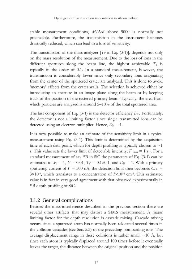
3.2.3 Doppler-broadening measurementsFigure 3-6 shows the normalized Doppler-broadening spectrum of an ionimplanted 4H-SiC sample together with one obtained from virgin material.The spectrum of the implanted sample is narrower than that of thereference sample indicating the presence of open volume defects, asdiscussed above. Doppler-broadening spectra are usually quantified by theline-shape parameters S and W, defined as
( )dEEkeVISs
s
E
E
+= �−
511N (3-8a)
( )dEEkeVIWW
W
E
E
+±= �±
±
5112
1
N , (3-8b)
3.2 Measurement techniques – PAS
28
where IN is the normalized Doppler spectrum intensity after subtraction ofthe background noise signal. The limits for the S parameter are chosensymmetrically around, and close to the 511 keV line to provide informationof annihilations with low momentum, valance electrons. As a rule of thumbthe limits should be chosen to give S ≈ 0.5 for a perfect crystal, whichtypically translates to a value for ES in the 1 keV range. The W parameter isdefined to describe annihilations with the high momentum core electronsof the annihilation site. The boundaries, EW1, 2, should the be chosen togive as little correlation with the S parameter as possible, but withoutsacrificing too much signal dynamics. Typical values for EW1 and EW2 are 3and 7 keV, respectively. The W integral may be performed on both sides ofthe 511 keV line to maximize the data usage, although this implies a verycareful compensation for the highly unsymmetric background level, whichcan be seen in Fig. 3-6. There are no standards for the choice of S and Wintegration limits, nor for the background reduction, which again meansthat it is difficult to compare results obtained by different research groups.A standard would perhaps not be very meaningful anyway, since theDoppler-spectra themselves also may differ from system to system, mainlydue to the resolution of different detectors. To minimize this problem, W
S
WW
2Es
511+ EW1
keV511 EW2
keV-
511+ EW2
keV511 EW1
keV-
W
Figure 3-6 Normalized Doppler-broadening spectra of a virgin (dotted line) and Al+ implanted(solid line) 4H-SiC sample. The integration intervals for the S and W parameters are included asvertical lines. No subtraction of the background signal has been made.

Hydrogen diffusion and ion implantation in silicon carbide
29
and S are frequently given as normalized to their corresponding values forundamaged bulk crystals, i.e., S/Sb and W/Wb.
Each type of annihilation site, bulk crystal, sample surface, or variouspositron traps, has a characteristic Doppler-broadening spectrum with acorresponding (S, W ) state. The Doppler-broadening spectrum obtained ina measurement is a superposition of all annihilations in the sample, and themain advantage of quantifying spectra according to Eq. (3-8) is that theextracted S and W parameters are the superposition of all the individualline-shape parameters:
( ) ( ) ( ) ( )
( ) ( ) ( ) ( )
,1
,
,
=
++=
++=
�
�
�
ζζη
ηηη
ηηη
d
d
WEWEWEEW
SESESEES
ddssbb
ddssbb
(3-9)
where the subscripts b, s, and d represents bulk, surface, and the differentdefect annihilation sites. E is the energy of the impinging positrons. Thefraction ηζ of the positrons that will annihilate at each state ζ is determinedby the positron implantation profile, the positron migration due todiffusion and drift, the defect concentrations, and the correspondingpositron trapping (and detrapping) rates. Figure 3-7 shows the normalizedS and W parameters as a function of the positron energy from a SPB-DOBS measurement of an 18 keV 11B implanted SiC sample together withthe one from a virgin sample. The top of the graph gives the expectedmean positron implantation range, Rpe+(E ), for SiC. For the highestenergies, S and W are close to the bulk values in both samples, but as theenergy decreases, bringing the implanted positrons closer to the samplesurface, S and W gradually increase and decrease, respectively. Thebehavior of the reference sample is understood by considering thedependence of Rpe+(E ) on the fraction of implanted positrons that candiffuse back to the surface instead of annihilating in the bulk. In fact, thistype of back-diffusion experiment of virgin samples can be performed toextract the positron diffusion constant, which in this case was determinedto D+ = 7 cm2/s. In the implanted sample the appearance of implantationinduced vacancy type defects is revealed around E ≈ 2 keV as a distinctmaximum and minimum in S and W, respectively. This energy translates to

3.2 Measurement techniques – PAS
30
a projected range for the implanted positrons of 30 nm, in good agreementwith the predicted projected range for vacancies created by 18 keV 11B inSiC [Paper IX].
As opposed to the lifetime measurements, the characteristic annihilationproperties of individual defects (Sd, Wd) can not be directly determinedfrom a DOBS measurement. To still make the identification of the defectstates possible, S(E ) and W(E ) can be depicted in a S versus W diagram.When only two types of annihilation states are present for a range ofpositron implantation energies, the S and W will form a straight line-segment between the two states in the S(W ) plot. This result is obtaineddirectly from Eq. (3-9) assuming two annihilation sites, and with theannihilation fractions ηζ changing as a function of positron energy. As aconsequence, an annihilation state may be identified at the point where twoline segments meet. This is exemplified in Fig. 3-8, where a defect state t1 ina series of implanted SiC samples (see Paper IX for details) has beenidentified at (S/Sb = 1.060, W/Wb = 0.85). Between the bulk state (S/Sb =1, W/Wb = 1) obtained for the highest positron energies (see Fig. 3-7), andthe defect state t1, occurring for positron energies giving Rpe+(E) in the highconcentration damage area, the positrons only annihilate in the bulk or at
Figure 3-7 Annihilation line shape parameters Sand W as a function of implanted positron energyfor a virgin (●), and an 18 keV 11B implanted (□)4H-SiC sample. The upper scale shows theprojected range of the implanted positrons. Thesolid lines represent simulated spectra with defectprofiles according to Fig. 3-10.

Hydrogen diffusion and ion implantation in silicon carbide
31
the t1 defect. At lower energies positrons also annihilate at the samplesurface, but for these energies annihilation only takes place at t1 or at thesurface, giving a straight line between the t1 defect and the surfaceannihilation state. Fig. 3-8 also includes the S and W from a virgin sample.Here no defects are present and annihilation only takes place in undamagedbulk material or at the sample surface, thus forming a line between thosestates. Together with the implanted samples a closed triangle is formed inthe S(W ) plot. At the corners of this triangle all positrons annihilate at asingle site, i.e. ηζ = 1.
S versus W plots can also be used to monitor the transformation of defectsin a sample, for example in isochronal, S/W = S/W(T ), or isothermal, S/W= S/W(t ), annealing studies. It should also be mentioned that straight linesmay occur in a S(W ) plot with more than two defects present. For examplewhen different defect states are positioned on the same line or when twoout of three states preserve their respective annihilation fractionindependent of E. To accurately determine a (S, W ) defect state, manydifferent samples should be used, which all give saturation trapping for thesame S and W values.
bulk
surface(etched)
(etched)
defect
Figure 3-8 Normalized S versus W plot for a series of implanted (*), implanted and etched(+,▷), and virgin (◀) 4H-SiC samples. For details, see Paper IX.
3.2 Measurement techniques – PAS
32
The identification of an established (S, W ) defect state with a specificdefect configuration is considerably more problematic than for positronlifetimes. Calculations of the W parameter for defects have beenperformed, but so far agreements to the experimental values have onlybeen qualitative − at best. However, some clues to the identity of a defectstate can be obtained from the high momentum, core electron part of aDoppler-broadening spectrum. Different atoms have different electronicshell structures and it is therefore possible to obtain information about thechemical surrounding of a positron trap. To accomplish this thebackground noise level has to be substantially reduced compared to astandard single detector DOBS measurement. This can be accomplishedusing a two-detector setup, a so-called coincidence measurement, whichunfortunately is a very time consuming technique, since most of thedetected annihilation data is discarded. This technique can be used toidentify the sublattice of a vacancy in a compound material, or a vacancy-impurity complex. For details of the coincidence measurement technique,see for example Ref. [52].
3.2.4 Extraction of defect profilesIn the previous section it was shown that features in the S(E ) and W(E )profiles could be related to features of the defect profile by considering theprojected range of the implanted positrons. By simulating the implantation,migration, and trapping of the positrons it is also possible to gain a moredetailed picture of defect distributions from SPB-DOBS measurements.The extraction of defect profiles is performed by a least square fitprocedure of Eq. (3-9) to the experimental spectra. This is a rather complexiterative process where it can be difficult to assert the uniqueness of aparticular solution.
The first step in this process is to determine the different (S, W )annihilation states that are present in the sample. This can for example bedone using an S(W ) plot as described above. The S and W versus E spectraare then simulated by calculating the annihilation fractions at each site, ηζ,as a function of positron energy. The annihilation fractions are synonymousto the flux of positrons that annihilate at each state, Fζ, normalized to thetotal positron flux injected into the sample, I0, i.e., ηζ = Fζ/I0. The totalflux of positrons annihilating in undamaged material:

Hydrogen diffusion and ion implantation in silicon carbide
33
�∞
=0 b
b τCdxF , (3-10)
where C is the concentration of positrons at depth x from the samplesurface. With no detrapping of positrons, the annihilation flux at a defect dis similarly given by
�∞
=0
CdxCF ddd µ , (3-11)
where Cd is the defect concentration profile, and µd is the correspondingtrapping coefficient. Typical values for µd at 300 K are in the 10-9−10-7
cm3/s range depending on type of defect and its charge state [52]. The fluxof positrons annihilating at the surface can be determined considering thesurface boundary condition, or by using the conservation constraint for ηin Eq. (3-9). The problem is thus reduced to determining the positronconcentration profiles for each positron implantation energy. This isaccomplished by solving the steady state transport equation for positrons,which includes diffusion, drift, and trapping at various defects of theimplanted positrons, see Appendix A for details.
The positron implantation profile Ip(x, E) is usually approximated by a so-called Makhov distribution which originally was developed for describingelectron penetration [52, 53]. The distribution is a function of the targetdensity ρ, as well as a number of empirical parameters. A set of parametershas been extracted that gives reasonable accuracy for most materialsalthough it is preferable to use Makhov distributions that have beenspecifically developed for the studied material. The accuracy of an extracteddefect profile can never be better than the precision of the Ip(E) profiles.The positron implantation profiles are unfortunately rather broad, whichlimits the spatial resolution of the extracted defect profiles. The rangestraggling of Ip is typically of the same magnitude as the projected range.This is illustrated in Fig. 3-9, which depicts the predicted positron profilesin SiC for energies up to 40 keV.
Once the annihilation fractions ηζ(E) have been determined, the S(E) andW(E) profiles can be calculated from Eq. (3-9). The simulated spectra arecompared to the experimental ones and, after modification of the defectprofiles, the procedure is repeated until a satisfactory agreement is obtained.

3.2 Measurement techniques – PAS
34
In these iterations all factors that affect the simulated spectra can be used asfitting parameters, but it is important to keep the number of freeparameters to a minimum. This also includes the number of parametersthat describe the defect distributions, which therefore are typically given assimple box shaped profiles. With a large number of fitting parameters it isalways possible to obtain good fits to the experimental spectra, but usuallyon the expense of the physical relevance of the solution.
There are a number of available program packages dedicated to theextraction of defect profiles from SPB measurements, for instance theVEPFIT code [54]. For this thesis, however, a new code has beendeveloped, written in the high level mathematical programming languageMATLAB. The heart of any such code is the swift and accurate solving ofthe positron transport equation. An effective algorithm that accomplishesthis is given in Appendix A.
Figure 3-7 includes the simulated S(E ) and W(E ) spectra that provided thebest fits (S and W simultaneously) to the experimental data. For thereference sample, no defects were included in the simulations, and apositron diffusion constant of 7 cm2/s was obtained from the fit. For the11B implanted sample two defects were postulated [Paper IX], and the
25 10 keV 20 keV 40 keV
Positron implantation profiles in SiC
Figure 3-9 Positron implantation profiles in SiC predicted using Makhov distributions withstopping parameters as determined for Si [53] combined with the density of SiC, ρSiC = 3.21g/cm-3.
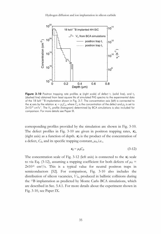
Hydrogen diffusion and ion implantation in silicon carbide
35
corresponding profiles provided by the simulation are shown in Fig. 3-10.The defect profiles in Fig. 3-10 are given in positron trapping rates, κd,(right axis) as a function of depth. κd is the product of the concentration ofa defect, Cd, and its specific trapping constant, µd, i.e.,
κd = µdCd. (3-12)
The concentration scale of Fig. 3-12 (left axis) is connected to the κd scaleto via Eq. (3-12), assuming a trapping coefficient for both defects of µd =2×10⁻⁸ cm3/s. This is a typical value for neutral positron traps insemiconductors [52]. For comparison, Fig. 3-10 also includes thedistribution of silicon vacancies, VSi, produced in ballistic collisions duringthe 11B implantation as predicted by Monte Carlo BCA simulations, whichare described in Sec. 5.4.1. For more details about the experiment shown inFig. 3-10, see Paper IX.
18 keV B implanted 4H-SiC11
Figure 3-10 Positron trapping rate profiles κt (right scale) of defect t1 (solid line), and t3(dashed line) obtained from least square fits of simulated PAS spectra to the experimental dataof the 18 keV 11B implantation shown in Fig. 3-7. The concentration axis (left) is connected tothe κt axis by the relation κt = µdCd, where Cd is the concentration of the defect and µd is set to2×10-8 cm3s-1. The VSi profile (histogram) determined by BCA simulations is also included forcomparison. For more details see Paper IX.
3.2 Measurement techniques – PAS
36
3.2.5 PAS measurements in SiCAn increasing number of experimental as well as theoretical PAS studies ofbulk and irradiated SiC has been published over the past 5−6 years. Startingwith undamaged, virgin material the experimental bulk lifetime, τb, istypically determined to be 142 ps with just a few ps in variation betweendifferent research groups and different types of SiC material [51, 55-59].This value is in good agreement with the one obtained in differentcomputational efforts: Brauer et al. give τb = 141 ps [56], while Staab et al.obtained a somewhat lower value, τb = 131 ps [60].
Considerably greater variations have been found for the positron diffusionconstant, D+, determined from SPB back-diffusion experiments asdescribed in the previous section. A compilation of experimentally andtheoretically extracted D+ in as-grown SiC is presented in Table 3-I. Thelowest values, around 0.3 cm2/s, are a great deal smaller than the highestexperimental values, 3−7 cm2/s, as well as the theoretically estimated valueof 4 cm2/s. The two lowest quoted D+ values were both obtained fromsubstrate material, as opposed to epitaxial SiC used in the otherexperiments. Therefore, it seems reasonable that the large variation in D+ isrelated to the crystalline quality and impurity content, which are known tobe significantly higher and lower, respectively, for epitaxial compared tosubstrate SiC. For instance, Polity et al. [58] has reported the existence of ashallow positron trap in as grown 6H-SiC doped with N to a concentrationof 5.4×1017 cm-3 (the type of material was not given although the dopinglevel suggests that substrate material was used). The positron bindingenergy of this trap was determined to 170 meV, which means that it is fairlystable at 300 K. The presence of this defect in a back-diffusion experimentperformed at 300 K would hence limit the diffusion length of the positrons,which would explain the material dependence of the extracted D+. Theidentity of this shallow trap has not been asserted but it is most likely notrelated to an ionized acceptor, which is expected to have a significantlylower binding energy [61]. Furthermore, the defect was found to be verythermally stable but did eventually anneal out at a temperature of 1740 K[58]. This gives further support for the assumption that the shallow trap isnot related to a doping atom.

Hydrogen diffusion and ion implantation in silicon carbide
37
TABLE 3-I Compilation of experimental and theoretical positron diffusion constants D+ inundamaged SiC. The experimental D+ are calculated from D+ = L2/τb, where the effectivediffusion lengths L are determined from back-diffusion SPB experiments with an assumed meanpositron implantation projected range of Rp
e+ = 40E1.6/3.2 (nm). τb was set to 140 ps for all D+.
D+[cm2/s]
Material Author
Experimental0.3 6H-SiC, substrate,
n-typeBrauer et al. [62]
0.3 − 0.8 4H-SiC, substrate,semi−insulating
Beling et al.[63]
1.4 3C-SiC, epitaxial,n-type, 3×1016 cm-3
Uedono et al.[64]
1.8 6H-SiC, epitaxial,n-type, 5×1015 cm-3
Kawasuso et al.[51]
2.4 3C-SiC, epitaxial on Si,n-type, 1×1016 cm-3
Itoh et al.[65]
2.9 6H-SiC, epitaxial,n-type, 1×1017 cm-3
Barthe et al.[66]
4.5 6H-SiC, epitaxial,n-type, 3.5×1015 cm-3
Uedono et al.[67]
7a 4H-SiC, epitaxial,n-type, 5×1015 cm-3
Janson et al.[PaperIX]
Theoretical3.6−4.3 3C-SiC Panda et al. [68]
aThis value was obtained with Rpe+ = 27.5E1.7/3.2 (nm). A value of 10 cm2/s was obtained using
the same Rpe+(E) as used by the other authors.
A large number of irradiation studies have been performed in SiC.Unfortunately, no consensus regarding the characteristics of the variousannihilation centers or their identification has so far been achieved. This isillustrated in Table 3-II, which shows a literature summary of annihilationparameters (τ, S, W) in electron, proton, and heavier ion irradiated SiC. Allirradiations represented in Table 3-II were performed at 300 K, with theexceptions of the electron irradiated samples of Polity et al. (e) and Puff etal. (f) performed at 4 K and 77 K, respectively. Lifetimes are given both asaverage lifetimes τav [Eq. (3-7)] and, when decomposed spectra werepublished, as lifetime components with corresponding intensities. S and Ware given normalized to the respective bulk values.
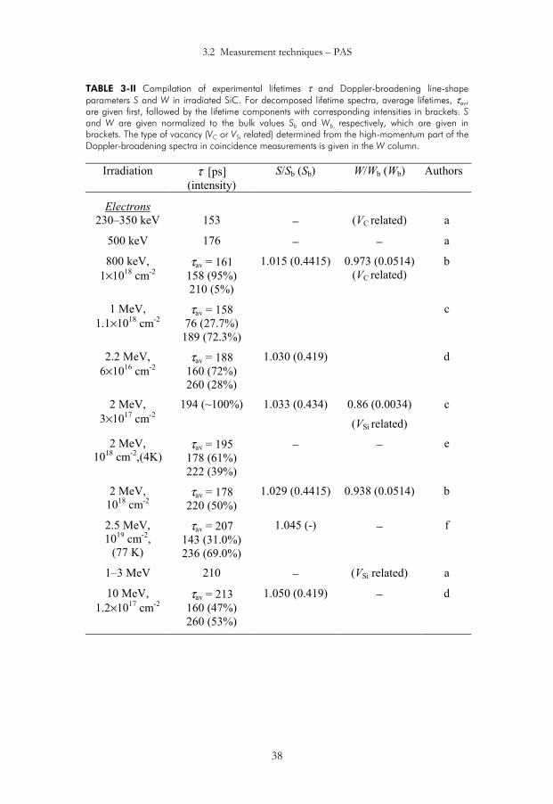
3.2 Measurement techniques – PAS
38
TABLE 3-II Compilation of experimental lifetimes τ and Doppler-broadening line-shapeparameters S and W in irradiated SiC. For decomposed lifetime spectra, average lifetimes, τav,are given first, followed by the lifetime components with corresponding intensities in brackets. Sand W are given normalized to the bulk values Sb and Wb, respectively, which are given inbrackets. The type of vacancy (VC or VSi related) determined from the high-momentum part of theDoppler-broadening spectra in coincidence measurements is given in the W column.
Irradiation τ [ps](intensity)
S/Sb (Sb) W/Wb (Wb) Authors
Electrons230–350 keV 153 − (VC related) a
500 keV 176 − − a
800 keV,1×1018 cm-2
τav = 161158 (95%)210 (5%)
1.015 (0.4415) 0.973 (0.0514)(VC related)
b
1 MeV,1.1×1018 cm-2
τav = 15876 (27.7%)
189 (72.3%)
c
2.2 MeV,6×1016 cm-2
τav = 188160 (72%)260 (28%)
1.030 (0.419) d
2 MeV,3×1017 cm-2
194 (~100%) 1.033 (0.434) 0.86 (0.0034)
(VSi related)
c
2 MeV,1018 cm-2,(4K)
τav = 195178 (61%)222 (39%)
− − e
2 MeV,1018 cm-2
τav = 178220 (50%)
1.029 (0.4415) 0.938 (0.0514) b
2.5 MeV,1019 cm-2,
(77 K)
τav = 207143 (31.0%)236 (69.0%)
1.045 (-) − f
1–3 MeV 210 − (VSi related) a
10 MeV,1.2×1017 cm-2
τav = 213160 (47%)260 (53%)
1.050 (0.419) − d

Hydrogen diffusion and ion implantation in silicon carbide
39
TABLE 3-II continued from previous page.
Irradiation τ [ps](intensity)
S/Sb (Sb) W/Wb (Wb) Authors
Protons5 MeV,
1016 cm-2τav = 209
144 (33.5%)242 (66.5%)
1.047 (−) − f
12 MeV,8×1016 cm-2
210 (100%) 1.058 (0.4415) 0.870 (0.0514)
(VSi related)b
150 keV,4×1016 cm-2
− 1.063 (0.453) 0.855 (0.0416) g
Heavier ionsN2
+, 100 keV,1×1013 cm-2
215 1.059 (0.459) −h
Al+, 100 keV,1×1013 cm-2
219 1.058 (0.459) −h
P+, 200 keV,1×1013 cm-2
223 1.067 (0.457) −h
Ge+, 200 keV,1×1013 cm-2
τav = 210235 (80%)
− −i
Ge+, 200 keV,1×1014 cm-2
τav = 234220 (92%)400 (8%)
1.068 (0.474) −i
Xe+, 124 MeVand neutronirradioation
225(plateau indose-study)
− −j
Al+, N+, B+, asimplanted and
etchedsamples
− St1 = 1.060(0.480)
St2 = 1.070(0.480)
Wt1 = 0.850(0.0326)
Wt2 = 0.820(0.0326)
k
aRempel et al.[69], bArpiainen et al.[57], cKawasuso et al.[51, 70], dDannefaer et al.[55], ePolityet al.[58], fPuff et al.[59, 71], gBarthe et al.[66], hUedono et al.[64, 72], iBrauer et al.[56, 62], j
Girka et al.[73], k Janson et al [Paper IX]

3.2 Measurement techniques – PAS
40
For the heavier ion implantations where only Doppler-broadening data waspublished, only results are quoted where either the shape of the S(E ) andW(E ) profiles, the dose development, or an S(W ) plot suggests that the Sand W originate from saturation trapping at one defect. The type ofvacancy (VC as opposed to VSi or VCVSi), determined by comparingexperimental and theoretical high-momentum parts of the Doppler-broadening spectra, are given in the W column for experiments using thecoincidence measurement technique.
Table 3-II gives a good illustration for the difficulty of decomposinglifetime spectra in a reproducible way. For example, compare the lifetimecomponents obtained from the 800 keV electron irradiation of Arpiainen etal. [57] to that at 1 MeV reported by Kawasuso et al. [70]. While Arpiainen etal. obtained two components of 160 and 210 ps, Kawasuso et al. extractedthe corresponding lifetimes to 76 and 189 ps. On the other hand, theaverage lifetimes of the two groups are quite similar, 161 and 158 ps, whichsuggests that the difference in the decomposed values are not due to theirradiations or the used materials, but rather to the decomposition itself.
Out of the many different lifetime components represented in Table 3-II,mainly two groups are possible to isolate: (i) (158 ±5) ps [55, 57, 69] and (ii)(218 ±8) ps [57, 58, 62, 64, 69, 72, 73]. Coincidence measurements,theoretical lifetimes (see below), and the electron energy dependence allsupport the assignment of the (158 ±5) ps annihilation center to the VC.On the other hand, the identification of the (218 ±8) ps defect has raisedsome diverging opinions. Arpiainen et al. [57] have identified their 210 psdefect to a VSi while Brauer et al. [62], Polity et al. [58], Uedono et al.,[64,72], and Ling et al. [74] suggest that their 215-232 ps defects originate fromthe VSiVC divacany. This latter view is shared by Kawasuso et al. whoascribe their 189-194 ps lifetime positron trap to the VSi [51, 70]. Oneimportant contribution to this identification is the finding that the 232 ps[74] and 222 ps [58] lifetimes are thermally stable up to 1400°C inagreement with an expected very high stability for the VSiVC divacany [75].
The (S, W ) states of the samples with saturation trapping at one defect alsoseem to fall into two groups: (i) t1 = (1.059 ±0.001, 0.86 ±0.01) [57, 64, 66,Paper IX], which was identified as a VSi by Arpiainen et al. [57], and (ii) t2 =(1.0685 ±0.0015, 0.82) [62, 72, Paper IX], identified as VCVSi by Brauer etal. [62]. By comparing the radiation conditions for these samples, oneinconsistency may be found: The 100 keV Al+, 1×1013 cm-2 implanted

Hydrogen diffusion and ion implantation in silicon carbide
41
sample from Uedono et al. gives an S value of 1.058, close to the t1 defect,while an equally implanted sample reported in Paper IX gives a value of S= 1.070, i.e. that of t2. It is likely that the difference between t1 and t2 (∆S =0.010) is too small to be accurately separated in the measurements of twodifferent research groups. It is important to point out, however, that twodifferent defects exist around t1 and t2, as shown in Paper IX, although theabsolute values (even after normalization) may shift somewhat in differentsystems. The (S, W ) state for the VC may be determined from the 800 keVelectron irradiated sample [57]: (S, W )VC = (1.013, 0.979), assuming a 5%contribution from t1 in the experimental values.
As already mentioned, theoretically determined lifetimes play an importantrole in the identification of positron defects, and the above quotedassignments were mainly done by comparing the experimental lifetimes tocalculated ones. Table 3-III shows a compilation of theoreticallydetermined positron lifetimes and binding energies, Eb, for free positronsand for positrons trapped in various intrinsic defect configurations of SiC.The calculations show only small differences (≤ 3 ps) between differentpolytypes and nonequivalent defect configurations of the same defect. Thequoted data are average values when more than one structure for eachdefect was presented. The calculations from Staab et al. [60] take the latticerelaxation around the defects into account, while it is not considered in theworks from Brauer et al. [56, 76]. Staab et al. have also shown that the VC
on the one hand and the VSi and VSiVC on the other, have significantlydifferent signatures in the high momentum part of the Doppler-broadeningspectra, while the predicted difference between VSi and VSiVC, is mostlikely too small to be resolved experimentally.
By considering all the experimental and theoretical data described above, aleast-common-denominator model for the positron annihilation propertiesof the simplest intrinsic defects in SiC may be formulated. Table 3-IV liststhe mean values of the identified experimental lifetimes, which arecompared to the corresponding mean values of the two theoreticalcontributions [56, 60]. It is interesting to note that the average experimentalvalues are systematically ~10 ps higher than the corresponding theoreticallyvalues for all defects. The Doppler-broadening line-shape parameters forVSi and VCVSi in Table 3-IV are from Paper IX, since it is the only sourceto quote both S and W parameters for both defects.

3.2 Measurement techniques – PAS
42
TABLE 3-III Calculated positron lifetimes τ and binding energies Eb for bulk SiC and fordifferent intrinsic defect configurations. The calculations show only small differences (≤ 3 ps)between different polytypes and nonequivalent defect configurations of the same defect. Thequoted data are average values when more than one structure for each defect was presented.The calculations from Staab et al. [60] take the lattice relaxation around the defects into accountwhile it is not considered in the works from Brauer et al. [56, 76].
Configuration τ [ps] Eb [eV] Authors
bulk 131 0 a141 0 b
VC 137 +0.08 a153 -0.26 b
VSi 194 -2.0 a193 -2.4 b
VCVC 161 -0.58 bVSiVC 215 -2.6 a
214 -3.0 bVSiVSi 196 -2.6 b
2-VSiVC 254 -3.5 b3-VSiVC 286 -4.3 b4-VSiVC 321 -4.9 b
aStaab et al. [60], bBrauer et al. [56]
TABLE 3-IV Positron annihilation properties of bulk and intrinsic defects in crystalline SiC. Theexperimental lifetime values τexp represent mean values of identified lifetimes obtained from theliterature, while the corresponding theoretically determined values τtheory are average values fromthe works of Staab et al. [60] and Brauer et al. [56]. ∆τ gives the difference between theexperimental and theoretical values, ∆τ = τexp−τtheory. The Doppler-broadening line-shapeparameters for VC are from Arpiainen et al. [57] (after compensation for the 5% contributionfrom VSi), while the VSi and VCVSi values are from Paper [IX].
Configuration τexp[ps]
τtheory[ps]
∆τ[ps]
S/Sb W/Wb
bulk 142a,b,c 136 6 1 1
VC 157a 145 12 1.013 0.979
VSi 202b 194 8 1.060 0.850
VCVSi 223c 214 9 1.070 0.820
aRefs [55, 57, 69]bRefs. [51, 57]cRefs.[58, 62, 72, 74]

Hydrogen diffusion and ion implantation in silicon carbide
43
4 Hydrogen migration andcomplex formation in
semiconductors
4.1 Hydrogen-acceptor complex 444.1.1 Formation kinetics 444.1.2 Dissociation kinetics 47
4.2 Migration of hydrogen 544.2.1 Charge state 554.2.2 Migration in the presence of doping gradient 56
Hydrogen (H) is a highly reactive species in semiconductors and candrastically alter the electrical properties of a device. Surface dangling bondsas well as doping impurities have been found to be passivated by theformation of electrically neutral complexes with H. The study of hydrogenin semiconductors is not only driven by an academic curiosity for thesubject, but is also motivated by the possibility of actively modifying thematerial and by the fact that H is a common contaminant in many deviceprocessing steps. This chapter describes the nature of hydrogen-acceptorcomplexes in semiconductors and the reaction kinetics related to theirformation and dissociation. Furthermore, the difficulty of determining thediffusion constant for mobile H is discussed as well as the H charge stateand its implication on the migration behavior in the presence of dopinggradients.

4.1 Hydrogen-acceptor complex
44
4.1 Hydrogen–acceptor complexThe existence of a passivating H-acceptor complex was first suggested in1983 by Sah and co-workers [77] who studied the decrease in net chargecarrier concentration in B-doped silicon (Si). Further evidence for the H-Bcomplex in Si (H-B:Si) was given later that year by Pankove et al. [78]. Theconcept of an electrically neutral complex between a shallow acceptor and aH atom is easy to comprehend considering the “missing” electron of theacceptor and the un-paired 1s electron of H. Pankove et al. [78] suggested asimple model for the configuration of the H-B:Si complex where the Hatom is directly attached to a Si atom, near the bond center site between theSi and the B atoms, and where the B relaxes towards the plane of the threeneighboring Si to form a three-fold coordinated B-Si3 system. This modelwas later supported by the local vibrational mode (LVM) properties of thecomplex [79], as well as by total energy ab initio calculations [80]. Theprobability for the formation of a H-acceptor complex is further enhancedby the fact that H has been found to exist in a positive charge state in mostp-type semiconductors (see further in Sec. 4.2.1). This means that (i) theionized acceptor will exert a long range coulomb attraction force on themigrating H+, and (ii) no third particle, electron or hole, is involved in theformation of the complex. Since 1983, a large number of experiments for awide range of acceptor-semiconductor combinations have been performedto verify the existence, and to determine the dissociation energies of thecomplexes. In all of these experiments H has been found to form apassivating complex with the acceptor.
4.1.1 Formation kineticsIn an experiment where a H-acceptor complex is to be investigated, H istypically introduced in the surface region of the sample using a hydrogenplasma or low energy H+ ion implantation. If the temperature during thehydrogen treatment is sufficiently high for the H atoms to migrate, but nothigh enough to dissociate the H-acceptor complexes, a layer of fullypassivated acceptors gradually develops deeper and deeper into the sample.If the complex formation can be described by the theory of diffusionlimited reactions [81], the leading front of the passivated layer becomesexponential with the exponential slope α given by [Paper I]:

Hydrogen diffusion and ion implantation in silicon carbide
45
RX πα 40= (4-1)
where X0 is the initial acceptor concentration and R is the effective reactionradius of the H-acceptor complex. This type of H-acceptor complexformation is exemplified in Fig. 4-1, which shows the deuterium (2H) depthprofiles determined by SIMS in three B-doped 4H-SiC epitaxial layers thathave been implanted by 10 keV 2H+ and then annealed at 460 °C for 30min. The validity of Eq. (4-1) is qualitatively confirmed directly by studyingthe leading fronts of the out-diffused 2H profiles exhibited in Fig. 4-1:steeper exponential slopes are observed for samples with higher B-doping.By extracting α from a large number of B doped samples annealed at 460°C, an experimental effective reaction radius for the 2H-B complex in SiC atthis temperature was determined to RHB:SiC = (21 ±4) Å [Paper I]. Thisrelatively large capture radius suggests that the trapping mechanisminvolves a long range coulomb attraction between the B− and the mobileH+. As a first approximation, this coulomb force assisted reaction radius Rc
is often estimated as the distance r between the mobile H+ and the ionizedacceptor X−, where the coulomb potential energy loss V equals the thermalenergy,
TkR
eV Bc
Rr c === πε4
2. (4-2)
1015
1016
1017
1018
1019
1020
0 0.2 0.4 0.6
Con
cent
ratio
n(c
m-3
)
Depth (µm)
As implanted
B2
B1
B3
2 + - 2
oH + B H-B
3 SiC epi-layers at 460 C�
Figure 4-1 SIMS measurements of2H concentration versus depth (○) inthe 2H implanted B1, B2, and B3samples, as implanted andannealed at 460 °C for 30 min. TheB concentration in each sample isindicated by the horizontal dashedlines. The solid lines represent leastsquare fits of exponential functionsto the diffusion fronts.

4.1 Hydrogen-acceptor complex
46
Here e is the elementary charge, ε (=εrε0) the dielectric constant, kB
Boltzmann’s constant, and T the absolute temperature. Eq. (4-2) originatesfrom the theory of recombination in gases [82] and the direct adaptation tosolid state diffusion has not been thoroughly investigated. For example, onemight question the value of 1×kBT to represent the thermal energy. On theother hand, the Dulong and Petit value of 3kBT would certainly be too highconsidering that these experiments are conducted at temperatures far belowthe Debye temperature θD of the material. An effect that is not included inEq. (4-2) is the screening of the coulomb potential by free carriers in thesemiconductor. A simple way to include screening is to use a modifiedpotential, Vscr = e2/(4πεr)exp(−q0r) [83], where the reciprocal screening
length q0 for a free carrier gas of density n is given by Tkneq Bε/20 = .
The screening effect will thus shift Rc to lower values and dependsprimarily on the doping concentration. This is demonstrated in Fig. 4-2,which compares Rc using the un-screened and the screened potentials as afunction of carrier concentration for SiC at 460 °C, and for Si at 25 °C and80 °C, respectively.
Only a few experiments have been conducted where the effective captureradius for a H-acceptor complex has been determined. However, theapproximate Rc of Eq. (4-2) has proven to be in surprisingly goodagreement with the limited number of experimental R values. This isvisualized in Fig. 4-3 which shows the experimental values of εrR (εr is therelative dielectric constant) as a function of temperature for 1H-B:Si at 25°C [84] and 80 °C [85], and for 2H-B:SiC at 460 °C [Paper I]. The material
Figure 4-2 The effective reaction radius Rc fora positively and negatively charged pair,satisfying the relation Vr=Rc = kBT, as a functionof carrier concentration for an un-screened(dashed lines) and a screened potential (solidlines) for SiC at 460 °C, and for Si at 25 °Cand 80 °C, respectively.

Hydrogen diffusion and ion implantation in silicon carbide
47
independent εrRc = e2/(4πε0kBT) is drawn as a solid line in Fig. 4-3 and thegood agreement to the experimental data gives support for the general T-1
dependence of R and, to some extent, the choice of 1×kBT in Eq. (4-2).One contributing reason for this is given by the fact that coulombscreening is not expected to play a substantial role in any of the aboveexperiments. The acceptor concentrations in both Si experiments were1.4×1015 cm-3 [84, 85], while the RHB:SiC value was determined with a totalacceptor concentration of 1-7 ×1017 cm-3 [Paper I]. The calculated Rc usingthe screened potentials, as determined from Fig. 4-2, all fall within the givenaccuracy for each experimental R.
4.1.2 Dissociation kineticsOnce a complex has formed it may dissociate to its original componentsprovided that sufficient energy is transferred to the complex. This energybarrier for dissociation is commonly referred to as the dissociation energy,Ed, and is usually taken as the sum of the binding energy of the complex,Eb, and the migration energy (or enthalpy) of the mobile H, Em. Eb is heredefined as the energy difference between a crystal system with a H and anacceptor well separated from each other, and the system where the pair hasformed a complex. Em is the energy barrier between two neighboring Hlattice sites, separated by the jump distance λ. However, if the formalism
Figure 4-3 Effective reaction radius Rmultiplied by the relative dielectric constant εr
as a function of temperature. The markers givethe experimental values for the 1H-B complex inSi (●), at 25 °C [84] and 80 °C [85], and for2H-B in SiC (○) at 460 °C [Paper I]. The solidline represents the coulomb force assistedreaction radius determined from Vr = Rc = kBTwith an un-screened potential.

4.1 Hydrogen-acceptor complex
48
with an effective capture radius is to be maintained, Ed = Eb + Em does nothold exactly since the potential energy of a H atom after dissociation islower than Eb by the amount of the coulomb potential at r = Rc. With Rc
given by Eq. (4-2), the dissociation energy then becomes:
Ed = Eb + Em – kBT (4-3)
Figure 4-4 shows the schematic total potential energy as a function of theseparation r for a H-acceptor pair with Eb = 1.6 eV, Em = 1 eV, (i.e. withEd = 2.5 eV at 730 K) and λ = 2.5 Å. These values are chosen tocorrespond to the 2H-B complex in SiC, as discussed below. Theunscreened coulomb potential as well as the reaction radius Rc for SiC at460 °C [Eq.(4-2)] are also included in Fig. 4-4. The potential energy followsthe coulomb potential until the H+ is roughly one jump distance away fromthe acceptor. Here the complex is formed and the energies of electronic(bond formation) and atomic reconfigurations around the complex areadded to the coulomb energy resulting in a total potential energy Eb.
T = 730 K: R Tc( )
Em
λ
k TB
Eb Ed
Figure 4-4 The schematic total potential energy as a function of the separation r (solid line)for a H-acceptor pair with Eb = 1.6 eV, Em = 1 eV, (i.e. with Ed = 2.5 eV at 730 K). Thesevalues are chosen to correspond to the 2H-B complex in SiC, as discussed below. Theunscreened coulomb potential (dashed line) as well as the reaction radius Rc for SiC at 730 K[Eq.(4-2)] are also included. The magnitude of the thermal energy kBT at 730 K is indicated inthe upper left corner.

Hydrogen diffusion and ion implantation in silicon carbide
49
The dissociation energy can be established experimentally by determiningthe temperature dependence of the dissociation frequency ν for thecomplex, which is expected to follow the Arrhenius equation:
ν = ν0exp(−Ed/kBT). (4-4)
ν0 is the so called attempt frequency and is closely related to thecharacteristic oscillation frequency of the lattice νlattice. One way to defineνlattice is to weight each vibration mode of the lattice, ωk, with the energy ofthat mode,
�
�==
kk
kk
n
n
�
�
ω
ω
πω
πν
2
21
21
lattice . (4-5)
Here �n� is the Planck distribution function, and � the reduced Planckconstant. Numerical integration of Eq. (4-5) with the dispersion relationgiven by the Debye approximation typically yield values for νlattice around1013 s-1. However, a H+ that has just been released from an acceptor has ahigher probability to be (re-) captured than a H+ at a random position inthe crystal. To account for this, a correlation factor, f < 1, is introduced: ν0
= f νlattice. Ideally, f only depends on geometrical entities (e.g. Rc, λ, and thecrystalline structure) but can only be determined by numerical simulations.
Two classes of experiments have been employed to determine ν(T) for H-acceptor complexes. In the most common method, pre-hydrogenatedsamples are thermally annealed in the presence of a strong electric fieldsupplied by a reversed biased Schottky contact. The H+ atoms, releasedfrom complexes, are then swept out of the depletion region by the appliedfield. With the concentration of mobile H+ greatly reduced in this region,recapture of H+ can be neglected and the concentration of complexes,[HX], is reduced according to the first order rate equation: ∂[HX]/∂t =−ν[HX]. The drawback of this method is that the electric field mayinfluence the trapping/dissociation kinetics and that it also has to be shownthat the recapture of H can be neglected. A typical example of such areverse bias experiment is given in Fig. 4-5, which shows the capacitance-voltage (CV) depth profiles of the net acceptor concentration at 530 K inpre-hydrogenated (2H) Al doped SiC using a reverse bias of 5 V [86]. Theacceptor concentration in the near surface region is seen to increase as a

4.1 Hydrogen-acceptor complex
50
function of time as the 2H-Al complexes gradually dissociate, while thereleased 2H+ is swept deeper into the sample. This results in decreasingacceptor levels outside the space charge region, which in this case reaches adepth of ~2 µm. In this experiment the dissociation energy of the 2H-Al:SiC complex was estimated to Ed = (1.75 ±0.1) eV.
The second class of experiments exploit the fact that the mass transport ofH in a trap rich material is entirely limited by the trapping and dissociationprocesses, as long as the concentration of complexes dominates over theconcentration of mobile H+ and there are with no electric fields present.With the total concentration of H substantially lower than the acceptorconcentration, X0, the effective (or apparent) diffusion constant Deff can beshown to follow [Paper I]:
0eff XR
Dπ
ν4
= . (4-6)
The dissociation frequency can then be calculated from the experimentallydetermined Deff, provided that the acceptor concentration and the effectivecapture radius R of the complex are known. Figure 4-6 shows how anoriginally delta-shaped 2H profile at the edge of a buried Al doped SiCepitaxial layer is redistributed as a function of time at a temperature of 350°C [Paper I]. The 2H of the annealed samples has formed Gaussian-shapedprofiles indicating that the 2H diffusion obeys Fick’s law with a constantdiffusion coefficient. By determining Deff from a wide set of samples, andwith R = Rc in Eq. (4-6), the dissociation energy for the 2H-Al:SiC complexwas determined to Ed = (1.61 ±0.02) eV [Paper I]. This value is in
0 1 2 3 4 Depth (µm)
Con
c ent
ratio
n ( 1
0 c
m)
15- 3
Figure 4-5 CV-depth profiles of the netacceptor concentration in 2H-passivated p-type SiC. The profiles were monitored with a10 min interval during annealing at 530 Kand with a reverse bias of 5 V, extending ~2µm into the material. From Ref. [86].

Hydrogen diffusion and ion implantation in silicon carbide
51
reasonably good agreement with the less precise value determined using thereversed biased Schottky method. For the system 1H-B:Si, Zundel andWeber have employed the two different experimental procedures in twoindependent studies [85, 87], and obtained practically identical dissociationenergies for that complex.
The dissociation of H-acceptor complexes has proven to be very well-behaved systems in the sense that the extracted dissociation frequenciesusually exhibit Arrhenius temperature dependencies for all measured ν,covering a range of up to 5 decades. This is shown in Fig. 4-7 where theextracted ν for 2H-Al:SiC and 2H-B:SiC closely follow straight lines in theArrhenius plot over the more than three orders of magnitude covered bythe experimental values. This means that Ed and ν0, can be determined to ahigh degree of accuracy and this has been done for a wide number ofacceptors in Si [85], GaAs [88-90], and SiC [Paper I]. Figure 4-7 includesthe fitted Arrhenius equations determined in these experiments. With theexception of the 1H-Mg complex in GaAs, all extracted pre-exponential ν0
fall in the range 1013 to 1014 s-1, with an experimental uncertainty of typically± 50-90%. A good correlation between the experimental ν0 and the latticevibration frequency can be viewed as an evidence that the activation energyobtained from the Arrhenius fit is identical to the dissociation energy of thecomplex. The extracted dissociation energies for the 1H-Al, 1H-Ga, and 1H-In complexes in Si all give the same value Ed = (1.42 ±0.02) eV [85], whichis only slightly higher than that for the complex with the smallest acceptor,1H-B:Si, Ed = (1.28 ±0.03) eV [85]. All of these H-acceptor complexes are
350oC anneal of pre-hydrogenatged Al doped SiC
4 h
1 h
27Al
initial H profile2
Figure 4-6 SIMS profiles of a 2H implanted,initially annealed (300 °C for 30 min), and 0.5µm ICP etched Al doped (dashed line) SiCsample. 2H profiles are shown as etched(dotted line) and after annealing (○) at 350 °Cfor 1 h and 4 h, respectively. The solid linesrepresent least square fits of Gaussianfunctions to the diffusion profiles. (The sum oftwo Gaussians are used to account for thereflective boundary condition at x = 1.4 µm.)The 2H background concentration of 1×10¹⁵
cm-3 has been subtracted from the 2H profilesin the figure prior to the Gaussian fittingprocedure.

4.1 Hydrogen-acceptor complex
52
expected to have the near bond centered (BC) configuration, where theinteraction between H and Si is stronger than that between H and theacceptor [85]. This explains why all these different complexes have sosimilar dissociation energies.
In GaAs the 1H-Si, 1H-C, 1H-Zn, and 1H-Be complexes also exhibit verysimilar dissociation energies, Ed = (1.2–1.4 ±0.1) eV, where Ed for the Assite group-IV acceptors (Si and C) are somewhat higher (~0.2 eV) than forthe group-II acceptors occupying a Ga site (Zn and Be) [88, 89]. Thesecomplexes have also been found to have a BC configuration and thedifference in Ed of the two groups can be qualitatively understoodconsidering that H has been shown to bond primarily to the Ga atom in theformer, but to the acceptor in the latter case [91]. The 1H-Mg complex inGaAs provides the exception to the above pattern, not primarily due to thelower dissociation energy, Ed = (0.90 ±0.03) eV, but mainly due to the fivedecades lower pre-exponential ν0 [90]. This different behavior couldperhaps be related to the observation that the 1H-Mg complex, in contrastto the above complexes, do not have a BC-configuration [92]. The
GaAs:
SiC: Si:
Figure 4-7 Arrhenius plot of the extracted dissociation frequencies for the 2H-Al (●) and 2H-B(■) complexes in 4H-SiC [Paper I]. Solid lines are least square fits of Arrhenius equations to theexperimental data. Also included are the corresponding Arrhenius equations extracted for avariety of 1H-acceptor complexes in Si (dashed lines) Ref. [85], and GaAs (dotted lines) Refs. [88,89, 91].

Hydrogen diffusion and ion implantation in silicon carbide
53
extremely low ν0 is, however, not easily explained and also obscures theinterpretation of the extracted Ed.
The H-acceptor dissociation energies in 4H-SiC are found to be higherthan those in Si and GaAs. As already mentioned, Ed = (1.61 ±0.02) eV for2H-Al:SiC, but the 2H-B complex is found to be even more stable: Ed =(2.51 ±0.04) eV [Paper I]. The authenticity of these values is supported bythe fact that although Ed differs by almost 1 eV, the extracted pre-exponentials, ν0, are almost identical for the two complexes (Fig. 4-7) andfall just below the characteristic lattice frequency of the SiC lattice, νlattice =1.6×10¹³ s-1 [Paper I]. A difference of 0.9 eV in Ed suggests that theconfiguration of the two complexes in SiC are significantly different.Unfortunately, no local vibrational mode data has yet been published toreveal the atomic configurations of these complexes. On the other hand, ina recent ab initio study by Aradi et al. the energetically most favorableconfigurations for the 1H-Al and 1H-B complexes in 4H-SiC werecalculated [93]. For the 1H-B complex they found that the H atom ispositioned at a BC site, forming a strong bond to the C atom [Fig. 4-8 (a)],similar to the H-acceptor configurations in Si and GaAs. In contrast, themost stable configuration for 1H-Al was found with the H at anantibonding site according to Fig. 4-8 (b). This could be qualitativelyunderstood considering that the H atom can not fit into the BC site in thedense, closed packed SiC lattice when the B atom was substituted by thelarger Al acceptor. Furthermore, the binding energies, Eb, of the 1H-B and1H-Al complexes were calculated to 1.6 eV and 0.7 eV, respectively. Thesetheoretical findings are convincingly supported by the experimental resultssince the difference between the calculated Eb are identical to the difference
(a) (b)
Figure 4-8 The geometry of the most stable 1H-B (a) and 1H-Al (b) complexes at thehexagonal site of 4H-SiC, as determined by ab initio super cell calculations. From Ref. [93].

4.1 Hydrogen-acceptor complex
54
between the empirically extracted Ed, in a agreement with Eq. (4-3). Bycombining the experimental and theoretical results, a migration barrier forH in 4H-SiC of Em = Ed − Eb + kBT ≈ 1 eV can be estimated. This valuefor Em should, however, be treated with some care since the absolute errorsin the calculated Eb are expected to be relatively large, as pointed out byDeák et al. [94].
4.2 Migration of hydrogenAccording to Fick’s law [95] the net flux of atoms A in random motion, Fr,is proportional to the negative concentration gradient of A, where theproportionality constant is identical to the diffusion coefficient, D, i.e. inthe one-dimensional case: Fr = −D ∂[A]/∂x. (Brackets denoteconcentration values of A.) The atomic flux originating from the drift ofparticles A of charge q in an electric field E, Fd, can also be shown to beproportional to D: Fd = qD/(kBT)E[A], due to Einstein’s relation betweenmobility and diffusivity. The gradient of the sum of the two fluxes gives thedifferential equation governing diffusion and drift
[ ] [ ] [ ]( )��
�
�
��
�
�
∂∂−
∂∂=
∂∂
xAE
Tkq
xAD
tA
B2
2, (4-7)
where D has been assumed to be independent on concentration. For anatom with an interstitial diffusion mechanism, typical for small atoms likehydrogen, the diffusion constant is given by
D = D0 exp(−Em/kBT) (4-8)
where the pre-exponential is only weakly temperature dependent andnormally falls in the range of D0 ≈ λ2νlattice. The migration energy, Em, canbe determined by establishing the temperature dependence of D. However,the intrinsic diffusion constant for hydrogen DH has proven to be verydifficult to measure at temperatures below ~1000°C. There are mainly tworeasons for this: (i) The solid solubility for isolated H in semiconductors isvery low, typically much below the sensitivity limit for any quantitativeanalysis method. (ii) In experiments where H is monitored, either by directtechniques (e.g. SIMS) or by indirect methods (e.g. CV-measurements), theoverwhelming majority of the detected H appear in the form of complexes,

Hydrogen diffusion and ion implantation in silicon carbide
55
such as H-acceptor pairs or H2 molecules. As a consequence, the mobilityof H detected at temperatures below ~1000°C is limited, not by DH, but bythe formation and dissociation properties of the dominating H-defectcomplex, as exemplified by Eq. (4-6). This independence of DH can bevisualized considering that the average time between de-trapping and re-trapping of H, i.e. the time that is determined by DH, is negligible comparedto the average lifetime of a complex.
Typically, DH can only be determined as the product DH[H] [Paper I] andsince [H] is normally not accessible, only a lower limit for DH can beestablished. In order to determine DH by monitoring the H migration, theconcentration of H must exceed that of the complexes. If ν, R, and DH areknown (or can be reasonably estimated) the relation
[ ][ ] [ ]X4HX
HHRDπ
υ= , (4-9)
may be used to determine the minimum temperature Tmin needed [Eqs. (4-3), (4-4), (4-8), and (4-9)] to fulfill the criterion [H]/[HX] > 1. Here X is apoint defect that forms a complex, HX, with a hydrogen atom. Thistemperature is usually very high as shown by the following example. ForSiC with an Al concentration, Al0, of 1019 cm-3, ν and R as determined inPaper I, Em = 1 eV, and with an assumed D0 of 0.01 cm2/s, Tmin becomes1500°C. (In this example [H]tot = [H] + [HAl] is assumed to beconsiderably lower than the concentration of Al so that [X] ≈ Al0 in Eq. (4-9).) However, at this temperature the diffusion length DtL = becomesmuch too large for reasonable annealing times t, to be determined by anyconventional surface technique such as SIMS or CV-measurements. Theexperimental difficulty of determining DH at temperatures below Tmin isillustrated by the fact that only one experiment has been conducted at thesetemperatures (1H in B doped Si at 300 K) where the extracted diffusionconstant is believed to represent the diffusivity of the mobile H atoms [84].
4.2.1 Charge stateThe migration of H in semiconductors is further complicated by the factthat H has been shown to occur in different charge states depending on theFermi level position. The occurrence of a positive charge state for mobileH in p-type Si was experimentally discovered in 1985 by Tavendale et al.[96]. By monitoring the active acceptor profile in pre-hydrogenated B

4.2 Hydrogen migration
56
doped Si under a reversed biased Schottky contact, they could concludethat H, released from H-B complexes, drifted along the applied field as apositively charged species. A few years later, Tavendale et al. [97] and Zhu etal. [98] simultaneously published evidence that H migrates as H− in n-typeSi. A positive and a negative H charge state has also been found in GaAs[88] while for SiC, only H+ has been clearly demonstrated so far [86]. Theseexperimental findings are in good agreement with computational ab initiostudies, which have predicted both a donor and an acceptor level forisolated H in many semiconductors. In Si [99], GaAs [100], GaN [101], and4H-SiC [93] a so called negative-U behavior has been predicted for H,which in this case means the H is transferred from a positive directly to anegative charge state (+/-) as the Fermi level rises in the band gap. For 3C-SiC, on the other hand, a small stability window for H0 has been suggested[94].
4.2.2 Migration in the presence of doping gradientsThe migration of charged H will not only by affected by externally appliedelectric fields, as illustrated in Fig. 4-5, but also by internal fields that arisedue to gradients in the doping [Paper II]. This effect is demonstrated in Fig.4-9 (a), which shows the SIMS profiles of three pre-hydrogenated SiCsamples annealed for 30–60 s at 650, 750, and 850 °C, respectively. Theepitaxially grown samples contain three buried Al doped regions and ahomogenous B background doping. The 2H SIMS profiles are compared totwo sets of computer simulations of the diffusion experiment in whichcomplex formation and dissociation with the Al and B in the layers havebeen taken into consideration. If drift of 2H+ in the field generated by thegradients in the Al profile is excluded in the simulations the agreement tothe SIMS profiles is poor, as demonstrated in Fig. 4-9 (b). On the otherhand, when drift of 2H+ is taken into account [Fig. 4-9 (c)], the simulatedand the experimental profiles are in much better agreement. For moredetails about this experiment, see Paper III.
When comparing the simulated profiles of Figs. 4-9 (b) and (c) it can beseen that one effect of the internal electric fields is to delay the spreading of2H into the sample, i.e. reducing the effective diffusion length. This effectcould therefore be used to study diffusion at higher temperatures thanotherwise imposed by the depth range of the measurement technique andL(T,t), as discussed above. This possibility was proposed in Paper II as a

Hydrogen diffusion and ion implantation in silicon carbide
57
way to determine DH using SIMS. 2H diffusion at 900 °C in a similarstructure as that in Fig. 4-9 was also demonstrated in this paper. However,it could later be shown (see the example above) that at 900 °C theconcentration of 2H-Al complexes is expected to clearly dominate that ofthe diffusing 2H+ for an Al concentration of 1019 cm-3. This means that the2H diffusion observed at 900 °C in Paper II was not limited by DH, apossibility that was also suggested the paper.
Another effect of internal electric fields is that the concentration of mobileH+ in equilibrium will not be homogenous through a sample, but will,instead, follow the profile of the acceptors [Appendix B]. When theacceptor, X, that gives rise to the built-in electric field also is the maintrapping center for the hydrogen, it can be shown that the measured profileof the total (chemical) hydrogen concentration, [H]tot, will have a quadraticdependence of the corresponding acceptor profile, X0 [Appendix B]:
[ ] [ ]( )2tot0tot HH −= Xk , (4-10)
Al Al Al
BB B
a) c)b)SIMS simulations without field simulations with field
Figure 4-9 (a) 2H SIMS profiles of pre-hydrogenated and etched Al doped samples (see also Fig.4-6), as etched (dotted line) and after RTA anneal at 650 °C for 60 s (××××), 750 °C for 60 s (●),and 850 °C for 30 s (□). Computer simulations of the 2H diffusion including 2H trapping anddetrapping at Al (solid line) and B (dashed line); without (b) and with (c) the drift of 2H+ in thefield generated by the Al doping gradients.

4.2 Hydrogen migration
58
where k is a proportionality constant. If the internal field would not havebeen considered, the corresponding expression to Eq. (4-10) would belinear.
The analytically deduced dependence of Eq. (4-10) is experimentallydemonstrated in Fig. 4-10 (a), which shows the SIMS profiles of 2H and Bin a 4H-SiC B doped staircase structure, implanted with 20 keV 2H andannealed at 800 °C for 4 h. The box-shaped profile of the 2H suggests thata state close to equilibrium has been reached, and it is clearly seen that the2H concentration dependency is stronger than proportional to the Bconcentration. To determine this dependency, the 2H concentration insidethe B staircase is plotted versus ([B] – [2H]) in Fig. 4-10 (b). A least squaresfit of a power function to the experimental data gives: [2H] ∝ ([B] – [2H])1.9,in close agreement with Eq. (4-10). Besides from elucidating the effect ofdoping gradients on the migration of charged species, this result also showsthat practically 100% of the mobile H are in the positive charge state underthe investigated conditions. This result agrees with the predicted position of
Fitted power function: 2x10 (B - H)17 1.92
20 keV H implantation + 800 C for 4 h anneal of B-
doped 4H-SiC
2
o
Figure 4-10 (a) 2H (solid line) and B (dotted line) SIMS depth profiles of a 2H implanted and800 °C for 4 h annealed 4H-SiC sample with a buried B staircase structure. (b) shows the samedata as in (a) but plotted as 2H versus (B – 2H) (●). A least squares fit of a power function (solidline) reveals an almost quadratic dependence of (B – 2H) on 2H.
(a)
(b)

Hydrogen diffusion and ion implantation in silicon carbide
59
the (+/−) level in the upper half of the 4H-SiC band gap [93], a conclusionthat could not have been obtained from reverse bias experiments.

5.1 Ion implantation – stopping power
60
5 Ion implantation,range and damage
distributions
5.1 Stopping power 615.1.1 Nuclear stopping, Sn 625.1.2 Electronic stopping, Se 65
5.2 Ion channeling 68
5.3 Implantation induced damage 74
5.4 Simulation of ion implantation 785.4.1 Monte-Carlo Binary Collision Approximation simulations 79
Ion implantation is a process that is widely used in the manufacturing ofsemiconductor electronic devices. Furthermore, energetic ions are also usedin various material analysis techniques. In these applications it is of greatimportance to be able to predict the distribution, the energy loss, and thedamage created by the implanted ions. This chapter describes thefundamental processes of the stopping of energetic ions in matter, how it isaffected by the crystal orientation, and how damage is created by the ions inthe target. A brief description of ion implantation simulations is given atthe end of the chapter.

Hydrogen diffusion and ion implantation in silicon carbide
61
5.1 Stopping powerThe retarding forces acting on an energetic ion in matter are commonlytreated in terms of stopping powers, dE/dRI, i.e. the differential kineticenergy loss with respect to the distance RI traveled by the ion. The stoppingcross section S is related to the stopping power via
S = 1/N (− dE/dRI),
where N is the atomic density of the target. With this definition the totalpath length R of an impinging ion with initial energy E0 is given byintegration,
�=0
0
1 E
SdE
NR . (5-1)
The implanted ion looses its energy by displacing the target atoms in elasticcollisions and by exciting the target electrons, referred to as nuclearstopping (Sn) and electronic stopping (Se), respectively. These two processescan in most applications be regarded as being independent of each otherand the total stopping cross section is thus the sum of the two, S = Sn + Se .The stopping power is strongly dependent on the kinetic energy E of theion. This is demonstrated in Fig. 5-1 which shows the energy dependenceof Sn and Se for 14N in SiC. At low energies nuclear stopping dominates, butas the ion velocity increases the cross section for elastic collisions decreases
Stopping cross sections for N in SiC14
vTFvF
Figure 5-1 The energy dependence of thenuclear stopping (Sn, broken line) andelectronic stopping cross section (Se, solid line)for 14N in SiC. The Fermi velocity vF, and theThomas-Fermi velocity vTF are shown as verticalsolid and dotted lines, respectively. Sn is equalto that predicted by Ziegler et al. [102], whileSe is the expression from Paper V,experimentally verified up to ~ vTF.

5.1 Ion implantation – stopping power
62
and the electronic stopping becomes the major stopping force. Themagnitudes of Sn and Se are also functions of ion type and of the targetproperties and, while Sn can be determined to a high degree of accuracy bytheoretical means, empirical corrections are usually needed to predict Se.
5.1.1 Nuclear stopping, Sn
All collision processes that result in kinetic energy transfer from theimplanted ion to the target nuclei are included in the nuclear stoppingpower. This means that the nuclear scattering can be fully described by apotential between the ion I and j target atoms, ( ),...,,,,, 2211 ZZZVV rrr III = ,where rx is the position of the nucleus of ion/atom x. Fortunately, thismany-body potential can, to a high degree of accuracy, be replaced by thesum of interatomic potentials between pairs of atoms
( )�=j
jZZrVV ,, II , (5-2)
where jr rr −= I is the interatomic distance. For head-on collisions,repulsion between the positive nuclei of the colliding atoms is thedominating scattering mechanism and the interatomic potential can beapproximated by the electrostatic potential between the positive charges ofthe ion and the target atom nuclei, V = Z1Z2e2/4πε0r, where e is theelementary charge and ε0 the permittivity of free space. This type ofscattering, known as Rutherford scattering, results in large angle deflectionsand light ions may even be deflected >90° from a target with heavier atoms(Rutherford backscattering). However, the probability for Rutherfordscattering is very small for energetic ions and for the vast majority of theion-target collisions, the interatomic potential will be considerably reduced,mainly due to the electronic screening of the two nuclei.
Numerous approaches have been used to calculate interatomic potentials.In the simplest methods, the electronic charge distribution is fixed and thedifferent contributions to the potential are calculated independently as afunction of the interatomic distance r. A more sophisticated way is to useself-consistent ab initio calculations, but these methods require considerablymore computer power. Ziegler, Biersack and Littmark calculated theinteratomic potentials for a wide number of atomic pairs using fixedHartree-Fock charge-distributions [102]. They generally found goodagreements to both self-consistent calculations and to experimental data.
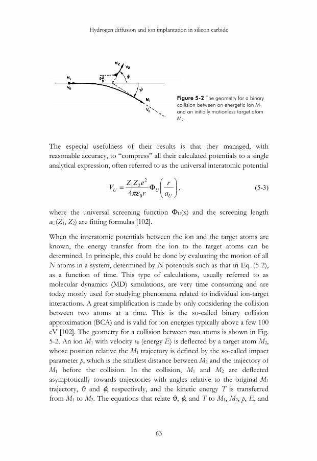
Hydrogen diffusion and ion implantation in silicon carbide
63
The especial usefulness of their results is that they managed, withreasonable accuracy, to “compress” all their calculated potentials to a singleanalytical expression, often referred to as the universal interatomic potential
���
����
�Φ=
UUU a
rreZZV0
221
4πε, (5-3)
where the universal screening function ΦU(x) and the screening lengthaU(Z1, Z2) are fitting formulas [102].
When the interatomic potentials between the ion and the target atoms areknown, the energy transfer from the ion to the target atoms can bedetermined. In principle, this could be done by evaluating the motion of allN atoms in a system, determined by N potentials such as that in Eq. (5-2),as a function of time. This type of calculations, usually referred to asmolecular dynamics (MD) simulations, are very time consuming and aretoday mostly used for studying phenomena related to individual ion-targetinteractions. A great simplification is made by only considering the collisionbetween two atoms at a time. This is the so-called binary collisionapproximation (BCA) and is valid for ion energies typically above a few 100eV [102]. The geometry for a collision between two atoms is shown in Fig.5-2. An ion M1 with velocity v0 (energy E) is deflected by a target atom M2,whose position relative the M1 trajectory is defined by the so-called impactparameter p, which is the smallest distance between M2 and the trajectory ofM1 before the collision. In the collision, M1 and M2 are deflectedasymptotically towards trajectories with angles relative to the original M1
trajectory, ϑ and φ, respectively, and the kinetic energy T is transferredfrom M1 to M2. The equations that relate ϑ, φ, and T to M1, M2, p, E, and
Figure 5-2 The geometry for a binarycollision between an energetic ion M1
and an initially motionless target atomM2.

5.1 Ion implantation – stopping power
64
V(r) were originally derived by J.J. Thomson in his work on electricalconductivity [103], but are equally relevant to scattering of two atoms:
( ) 2
2/12 1,0
��
���
�−−== �∞
rp
ErVg
grrp
cr
dφ , (5-4a)
φφϑ
2cos2sintan
21
2MM
M−
= , (5-4b)
( )φ2
221
21 cos4MMMMET
+= , (5-4c)
where EC = E/(1 + M1/M2). r0 is the so-called apsis of collision, which isthe smallest interatomic distance r in the collision and can be determinedfrom the equation:
g(r0) = 0. (5-4d)
With the final assumption that the ion reaches the asymptotic trajectorybetween consecutive collisions, the nuclear stopping cross section can bedetermined for a given interatomic potential using Eq. (5-4)
( ) ( )��∞∞
==00n d,2d pppETTES πσ . (5-5)
Using their universal potential, Ziegler et al. could extract a correspondinguniversal nuclear stopping cross section, SnZBL(E, Z1, M1, Z2, M2) [102]. Fig.5-1 shows the SnZBL prediction for 14N in SiC and the typical features ofSn(E) can be qualitatively understood as follows. For low ion energies (orion velocities) the target atom will have time to move away from theapproaching ion at an early stage in the collision. As the ion velocityincreases the colliding atoms will get closer to one another, resulting in anincreased (highest) potential during the collision and therefore an increasedT and Sn. At some velocity, the interaction time in the collision becomesthe limiting factor in the impulse taken up by the target atom. Eventually,this results in a decreasing stopping power as a function of ion energy.

Hydrogen diffusion and ion implantation in silicon carbide
65
5.1.2 Electronic stoppingIn semiconductor processing, ion implantations with energies up to severalhundred keV are normally used. Except for the lightest ions, these energiestranslate to ion velocities that are considerably lower than the averagevelocity of the target valence electrons, i.e. the Fermi velocity vF. The Fermivelocity is normally in the same order of magnitude as the Bohr velocity v0,which equals 2.19×108 cm/s or 25 keV/amu. In this low velocity regimethe target electrons induce a friction-like force on the ion and Se is thusanticipated to be proportional to the ion velocity v. Around 1960, twotheories for this low velocity electronic stopping were presented: that ofLindhard and Scharff [104, 105], and that of Firsov [106]. In the Lindhardand Scharff model, the inelastic energy loss is given as a mean stoppingcross section,
vZZ
ZZem
Se
2/33/22
3/21
26/7
12
3LSe
)(8
+= �π , (5-6)
where me is the electron mass, and � the reduced Planck constant. Firsov’smodel, on the other hand, gives the energy loss per collision, ∆Ee,depending on the impact parameter p
[ ]v
apZZZZemE e
50
3/121
3/521
2F
e/)(16.01
)(35.0+++=∆
�, (5-7)
where the Bohr radius a0 = �2/(mee2) ≈ 0.53 Å. Integration of Eq. (5-7)[similar to Eq. (5-5)] shows that the Firsov model gives comparablestopping to SeLS for Z1 ≈ Z2, but higher values when Z1 and Z2 differconsiderably. Generally SeLS has proven to be in better agreement toexperimental data [105]. However, the form of Eq. (5-7) with an impactparameter dependent electronic energy loss has proven to be useful inMonte-Carlo BCA simulations, where the energy loss is evaluated for eachcollision, as discussed in Sec. 5.4.1.
Both Eqs. (5-6) and (5-7), as well as later theoretical work [107], predict astrict velocity proportionality for the low-velocity stopping, i.e. Se ∝ Ep,with p = 0.5. (p is used for both the impact parameter and for the Se energydependence due to convention.) However, systematic deviations fromvelocity proportionality have been observed [102, 108-110, Paper V]. Figure

5.1 Ion implantation – stopping power
66
5-3 shows the experimental Se energy dependencies p as a function of Z1 inC [108, 109] and SiC [Paper V]. The extracted p show a very similardependency on Z1 in both materials, with p < 0.5 for Z1 ≤ 9 and p > 0.5 for13 ≤ Z1 ≤ 15. These deviations from velocity proportionality should not beconfused with those discussed in Ref. [105] for very low ion velocities. Notheoretical work has yet been presented that accounts for theseobservations of the low velocity electronic stopping.
Relatively soon after the publications of Eqs. (5-6) and (5-7) it wasexperimentally revealed that Se did not exhibit the monotonic Z1
dependence predicted by those models. This is exemplified in Fig. 5-4which shows experimental Se/v values as a function of Z1 for C [108] andSiC [Paper V], together with the corresponding Se/v of Eq. (5-6). Theexperimental Se for both C and SiC were extracted at a velocity of 0.41v0.Typically, local maxima in Se are found at Z1 = (6-8) and (17-18), whilecorresponding minima are located at Z1 = (11–13) and (30–32) [19, 108,111, Paper V]. These features are referred to as Z1-oscillations and havebeen attributed to the electronic structure of the impinging ions. Similarbehavior of Se is also seen as a function of target material, i.e. Z2-oscillations [112, 113]. Many contributions have been devoted to thetheoretical understanding of these phenomena [107, 114, 115]. In Ref. [107]the stopping power of an electron gas for slow ions was studied usingdensity-functional formalism (DTF), and in these ab initio calculations theZ1-oscillations for slow ions (v<vF) appeared in a natural way. In Fig. 5-4 we
velocity proportional Se
[108][109]
Figure 5-3 Exponent p for the lowvelocity electronic stopping, Se ∝ Ep,as a function of the ion atomicnumber Z1. The SiC data are fromPaper V while the carbon data areobtained from Refs. [108, 109].

Hydrogen diffusion and ion implantation in silicon carbide
67
have included their Se/v values of an electron gas with a density of 4.0×10²³
cm-3, which is close to the valence electron density of both SiC and C. TheDFT calculations show a distinct maximum at Z1 = 7 and a deep minimumaround Z1 = 12, in close agreement to the experimental data. Quantitativeagreement to the experimental data is reasonable up to Z1 ≈ 6, but forhigher atomic numbers the theory clearly underestimates the inelasticstopping. This observation, as well the observed higher stopping in SiCcompared to that in C, demonstrates the importance of the core electronsfor the low velocity electronic stopping. In this context it is interesting tonote that the DFT prediction of the Z1 behavior were considerably betterwhen compared to the electronic stopping for ions implanted in axialchanneling directions in Si [107]. This agrees with the fact that the influenceof the core electrons on Se is strongly reduced for channeled ions, asfurther discussed in Sec. 5.2.
For ion velocities larger than vF, the ion is gradually stripped off itselectrons and at velocities well above the Thomas-Fermi velocity, vTF =v0Z12/3, the ion will move as a bare nucleus through the target. At theseenergies the stopping rapidly decreases as a function of velocity (Fig. 5-1)according to the theory of Bethe and Bloch [116, 117],
[108]
Figure 5-4 Ratio of electronic stopping and ion velocity Se/v as a function of the ion atomicnumber Z1. The SiC values from Paper V (●) and the C stopping (○) from Ref. [108] areobtained at a velocity of 0.41v0. The experimental data are compared to the Se/v values of anelectron gas with a density of 4×1023 cm-3 (××××) calculated using Density Functional Theory (DFT)[107]. The Lindhard-Scharff (LS) values for SiC and C are shown as solid and broken lines,respectively.

5.1 Ion implantation – stopping power
68
Se
LZvm
eZS 22
4214π=BB
e , (5-8)
where LS is the so-called stopping number. For v > 2v0Z1 the stoppingnumber can be approximated by the Bethe formula LBethe = log(2mev2/Ie)[116], where Ie is the mean excitation energy typically on the order of Ie ≈10Z2 eV.
In the energy range between the low and high velocity regimes, around themaximum of Se located just above vTF, prediction of Se is complicatedmainly due to the partial stripping of the ion. In the velocity range betweenvF and vTF the stopping cross section will increase (relative to an unstrippedion) due to the higher effective charge of the ion seen by the targetelectrons (Fig. 5-1). Although some work has been devoted to this regime[118, 119] a quantitative theory describing the electronic stopping powerfor low and high mass ions, from low to high velocities is still missing. Fora recent review of electronic stopping powers see Ref. [110]
5.2 Ion ChannelingThe stopping powers discussed in the previous section are valid forimplantations where the ion follows a “random” trajectory through thetarget, so that all possible impact parameters are sampled in the collisions,i.e. dσ/dp = 2πp [Eq. (5-5)]. This is always true for ions implanted inamorphous targets but not necessarily in crystals, where rows of atoms inhighly symmetrical axial or planar directions form channels through thematerial. When an ion is injected into such a high symmetry direction it willbe steered towards the center of the channel since the atoms along the“channel wall” form a more or less continuos potential VCH = VCH(ρCH),where ρCH is the perpendicular distance between the ion and a row ofatoms in the channel. Due to this continuos potential the ion will start anoscillating movement along the channel, as sketched out in Fig. 5-5. Thiseffect is referred to as ion channeling and was first discovered about 40years ago in experiments, which revealed strong crystal orientationdependencies on sputtering yields, ion ranges, and backscattering yields[19]. The increased ion range, and the related reduced sputtering yield, isexplained by the fact that the nuclear stopping power for an ion with achanneling trajectory is considerably reduced, since close encounters are

Hydrogen diffusion and ion implantation in silicon carbide
69
effectively avoided. Furthermore, the electronic stopping power forchanneled ions will also be reduced since the average electron density islower in the center of a channel.
An ion that has started a channeling trajectory may be scattered out of thechannel again, referred to as dechanneling of the ion. Dechanneling in adefect free crystal happens when the transverse energy for the ion E⊥ =α 2E + VCH(ρCH) exceeds a critical value E⊥crit, where α is the anglebetween the instantaneous ion trajectory and the channel wall, see Fig. 5-5.With E⊥ > E⊥crit the ion comes too close to the target atoms for stablechanneling to continue. The initial E⊥ will increase during the oscillatingmovement since the gradient of VCH along the channel direction can not befully neglected. This is especially true when thermal lattice vibrations areconsidered; Lindhard has shown [120] that the rate of increased transverseenergy, with respect to the propagation x along the channel direction,depends on the mean vibrational amplitude <ux> as <dE⊥/dx> ∝ <ux>2.The thermal vibrations have furthermore been suggested to limit the valueof E⊥crit according to the relation E⊥crit = VCH(<ux>) [19]. Dechanneling isalso very sensitive to defects in the lattice, especially to interstitial typedefects. This property has been exploited in the widely used measurementtechnique Rutherford backscattering spectrometry in the channeling mode(c-RBS), which provides near surface disorder information of a sample. c-RBS is typically used for studying depth profiles of displaced atoms afterion implantation and for determining the lattice site location of heavydoping atoms in semiconductors.
The ion-channeling effect plays an important role for the range distributionof implanted atoms in crystalline semiconductors. The detailed shape of a
Channeling trajectory
"Random" trajectory
ρCH
α
Figure 5-5 An ion in a channeling trajectory (top) and an ion that propagates with a randompath (bottom) trough a crystal. The wave length of the channeled ion is highly underestimatedin this figure.

5.2 Ion implantation – ion channeling
70
given implantation profile is a complex matter and depends on the targetstructure and temperature, implantation direction, ion mass, energy,fluence, and flux. Figure 5-6 shows the (normalized) SIMS depth profiles ofnine implantations of 60 keV 27Al, each in a different direction relative tothe 4H-SiC crystal. The implantations were performed under low doseconditions, i.e. the damage produced by the previously implanted ions hasnot significantly affected the dechanneling probability for the subsequentions. Three of the implantations were performed parallel to major axialdirections [Fig. 5-6 (a)], while the remaining implants were performed at tiltangles 8-10° off a major axis. Four of the latter implantations were tilted ina major planar channel [Fig. 5-6 (b)], while the remaining two were tiltedtoward low symmetry directions [Fig. 5-6 (c)]. All profiles exhibit a peak ata depth of 0.07 µm, which coincides with the expected projected range fora corresponding random implant. This shows that a significant fraction ofthe Al beam becomes dechanneled close to the sample surface in allimplantations. The range of the (detected) deepest penetrating ions as wellas the fraction of channeled ions differ markedly between the variousdirections.
(a)
(b)
(c)
60 keV Al implanted in 4H-SiC27 +
Figure 5-6 Normalized range profilesof nine 60 keV Al implantations at 300K for different axial (a), planar (b), andlow symmetry (c) directions of 4H-SiC(see Paper VII for experimental details).All implantations were performedunder conditions where no dosedependence of the profiles wasobserved.

Hydrogen diffusion and ion implantation in silicon carbide
71
A qualitative understanding for the axial and planar channelingdemonstrated in Fig. 5-6 can be obtained by studying the atomic sequenceencountered by an ion in the different beam directions. Figure 5-7 showsthe Si and C atoms of the 4H-SiC crystal projected onto a planeperpendicular to each of the directions of the implantations represented inFig. 5-6. The most open of the different directions is the [ 0211 ] projection,
a) [0001] b) [1120] c) [1123]
e) 10 off [1120] in (0001) plane
od) 8 off [0001] in (1120) plane
o
g) 9 off [0001] in (1010) plane
o
f) 8 off [0001] in plane between
(1010) and (1120)
o
h) 10 off [1120] in (1010) plane
o i) 10 off [1120] in plane 55 off (0001)
o
o
Figure 5-7 The Si (○) and C (●) atoms of the 4H-SiC crystal projected on a planeperpendicular to various high and low symmetry directions of the crystal. The directionscorrespond to those of the 60 keV implantations in Fig. 5-6.
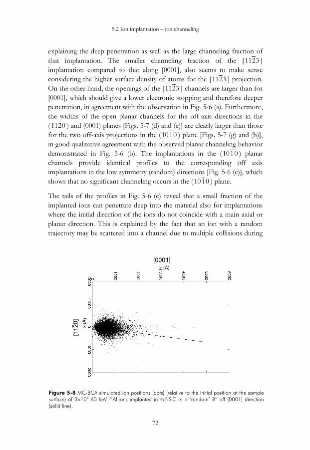
5.2 Ion implantation – ion channeling
72
explaining the deep penetration as well as the large channeling fraction ofthat implantation. The smaller channeling fraction of the [ 3211 ]implantation compared to that along [0001], also seems to make senseconsidering the higher surface density of atoms for the [ 3211 ] projection.On the other hand, the openings of the [ 3211 ] channels are larger than for[0001], which should give a lower electronic stopping and therefore deeperpenetration, in agreement with the observation in Fig. 5-6 (a). Furthermore,the widths of the open planar channels for the off-axis directions in the( 0211 ) and (0001) planes [Figs. 5-7 (d) and (e)] are clearly larger than thosefor the two off-axis projections in the ( 0110 ) plane [Figs. 5-7 (g) and (h)],in good qualitative agreement with the observed planar channeling behaviordemonstrated in Fig. 5-6 (b). The implantations in the ( 0110 ) planarchannels provide identical profiles to the corresponding off axisimplantations in the low symmetry (random) directions [Fig. 5-6 (c)], whichshows that no significant channeling occurs in the ( 0110 ) plane.
The tails of the profiles in Fig. 5-6 (c) reveal that a small fraction of theimplanted ions can penetrate deep into the material also for implantationswhere the initial direction of the ions do not coincide with a main axial orplanar direction. This is explained by the fact that an ion with a randomtrajectory may be scattered into a channel due to multiple collisions during
[0001]
[112
0]
(Å)
(Å)
Figure 5-8 MC-BCA simulated ion positions (dots) (relative to the initial position at the samplesurface) of 3×10⁴ 60 keV 27Al ions implanted in 4H-SiC in a ‘random’ 8° off [0001] direction(solid line).
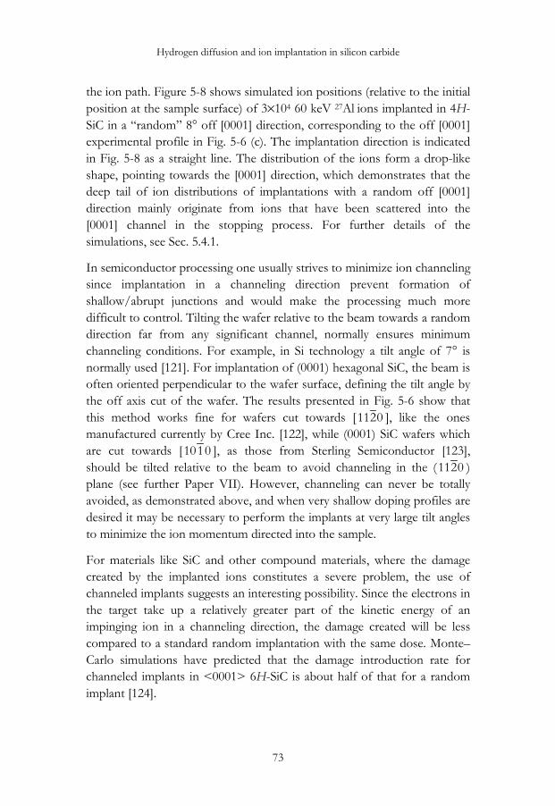
Hydrogen diffusion and ion implantation in silicon carbide
73
the ion path. Figure 5-8 shows simulated ion positions (relative to the initialposition at the sample surface) of 3×10⁴ 60 keV 27Al ions implanted in 4H-SiC in a “random” 8° off [0001] direction, corresponding to the off [0001]experimental profile in Fig. 5-6 (c). The implantation direction is indicatedin Fig. 5-8 as a straight line. The distribution of the ions form a drop-likeshape, pointing towards the [0001] direction, which demonstrates that thedeep tail of ion distributions of implantations with a random off [0001]direction mainly originate from ions that have been scattered into the[0001] channel in the stopping process. For further details of thesimulations, see Sec. 5.4.1.
In semiconductor processing one usually strives to minimize ion channelingsince implantation in a channeling direction prevent formation ofshallow/abrupt junctions and would make the processing much moredifficult to control. Tilting the wafer relative to the beam towards a randomdirection far from any significant channel, normally ensures minimumchanneling conditions. For example, in Si technology a tilt angle of 7° isnormally used [121]. For implantation of (0001) hexagonal SiC, the beam isoften oriented perpendicular to the wafer surface, defining the tilt angle bythe off axis cut of the wafer. The results presented in Fig. 5-6 show thatthis method works fine for wafers cut towards [ 0211 ], like the onesmanufactured currently by Cree Inc. [122], while (0001) SiC wafers whichare cut towards [ 0110 ], as those from Sterling Semiconductor [123],should be tilted relative to the beam to avoid channeling in the ( 0211 )plane (see further Paper VII). However, channeling can never be totallyavoided, as demonstrated above, and when very shallow doping profiles aredesired it may be necessary to perform the implants at very large tilt anglesto minimize the ion momentum directed into the sample.
For materials like SiC and other compound materials, where the damagecreated by the implanted ions constitutes a severe problem, the use ofchanneled implants suggests an interesting possibility. Since the electrons inthe target take up a relatively greater part of the kinetic energy of animpinging ion in a channeling direction, the damage created will be lesscompared to a standard random implantation with the same dose. Monte–Carlo simulations have predicted that the damage introduction rate forchanneled implants in <0001> 6H-SiC is about half of that for a randomimplant [124].

5.3 Ion implantation – damage
74
5.3 Implantation induced damageAs the kinetic energy of an implanted ion is gradually transferred to thetarget, damage is created in the lattice. In a conductor or a semiconductorthis damage mainly originates from elastic collisions between the ion andsingle target atoms, although complex many-body phenomena, such aslocalized melting [125] and even simultaneous coherent displacements ofatomic planes [126], are also known to occur. When the transferred elasticenergy T in a binary collision [Eq. (5-4)] exceeds a certain threshold valuethe target atom is displaced from its lattice position, thus creating a Frenkelpair, i.e. a self interstitial and a vacancy. This energy barrier, usually referredto as the displacement energy, Edisp, is strongly anisotropic and can varysubstantially for different materials, but is usually found to be in the 15–100eV range. Edisp can be experimentally determined by monitoring theminimum energy needed for creating defects by electron irradiation [127].In recent years Edisp has also been estimated theoretically using MD-simulations. In SiC, experimental results suggest the values EdispSi = 35 eVand EdispC = 20 eV for average displacement directions [127], where thevalue for Si displacements is less well established than that for C. Varioustheoretical studies seem to support these values [128, 129], although somecontroversy on the subject still remains [129].
A displaced atom recoils away from the primary ion trajectory with anenergy of T – Eb, where Eb is a binding energy in the range of 1-2 eV. Forcollisions with small impact parameters, this recoiling energy can besubstantial and the atom, also referred to as the secondary ion, has enoughenergy to travel far from its original position, displacing other atoms alongits path. In this way a stochastic cascade of defects is created by eachimplanted ion. This is exemplified in Fig. 5-9, which shows the BCA-simulated damage cascade created by a single 100 keV Al ion in 4H-SiC.The mean number of Frenkel pairs created in a cascade depends primarilyon the mass of the implanted ion. In SiC the average number of siliconvacancies, VSi, created by a 200 keV 1H+ ion is only 7, while 200 keV ionsof 4He, 11B, 27Al, and 75As result in 60, 250, 600, and 900 VSi, respectively.The energy of the implanted ion, on the other hand, has a relativelymoderate influence on the amount of damage produced. This can beunderstood considering that the implantation energy is usually significantly

Hydrogen diffusion and ion implantation in silicon carbide
75
higher than the energy that gives the maximum nuclear stopping crosssection (Fig. 5-1). This means that a further increase in implantation energywill only give a small increment to the total energy deposited in elasticcollisions. For 27Al in SiC, the Sn maximum appears around 10 keV and themean number of VSi per primary ion for Al implants at energies 1, 10, 100,1000, and 10 000 keV are 6, 60, 360, 1100, and 1800, respectively. For thedistribution of the damage, however, the energy is an important parameter.(The above calculations were performed by Monte-Carlo BCA simulationswith the full cascade damage algorithm, as described in Sec. 5.4.1.)
Implantation related defects are not limited to the elementary point defectsdescribed above, i.e. self-interstitials and vacancies. Both vacancies andinterstitials can form complexes with one another and with impurities in thecrystal. The formation and annealing kinetics of implantation relateddefects is, however, a very complex affair. Non-elementary defects may beformed in the ps time scale of the damage cascade evolution andthermalization process. Complex defects may also be formed during thecourse of the entire implantation when the sample as a hole is in an excitedstate with an abundance of electron-hole pairs and phonons. It is alsoknown that a substantial part of the produced Frenkel pairs, around 95% inSi, annihilate during a typical implantation [130]. Furthermore, the
100 nm
Figure 5-9 The damage cascade created by a single 100 keV Al ion (●) in 4H-SiC, predictedby a MC-BCA simulation. IC and ISi are shown as (●) and (●), while VC and VSi are shown as(●) and (●). A box with sides of 400 Å and a thickness of 20 Å is indicated, see further Fig. 5-11.

5.3 Ion implantation – damage
76
formation of certain defects is greatly enhanced if the ion is implanted in analready defected area, so-called overlapping cascades. Damage recovery andformation of tertiary defects also occur during post-implantationtreatments, for instance thermal annealing. It is therefore obvious thatdifferent combinations of implantation conditions such as ion mass andenergy (size and density of damage cascades), implantation dose(probability for overlapping cascades), dose rate (time for annealing ofdefects between potentially overlapping cascades), and implantationtemperature (migration, formation, and dissociation of the defects) have asignificant influence, not only on the number, but also on the types ofdefects that are generated.
The influence of implantation dose on the nature of created defects isillustrated in Fig. 5-10, which shows the Doppler-broadening line shapeparameter W/Wb as a function of implantation dose for 100 keV Alimplantations at 300 K in 4H-SiC. The positron annihilation events wereregistered using a 3 keV positron beam to obtain the same projected rangefor the positrons as for the implanted Al. At a dose of 1×1012 cm-2, W/Wb
is close to the value for the t1 defect, which has tentatively been identifiedas the silicon vacancy VSi [Paper IX, Sec. 3.2.5]. For doses between 1013
and 1014 cm-2, W/Wb is pinned to the value of t2, which has been suggestedto represent a silicon-carbon divacancy, VSiVC [Paper IX, Sec. 3.2.5]. When
t2
t1
WW/
b
100 keV Al RTimplantation in 4H-SiC
+
a-SiC
Figure 5-10 Normalized Doppler-broadeningline shape parameter W/Wb as a function ofimplantation dose for 100 keV Al implants at 300K in 4H-SiC (●). The positron annihilation eventsare registered using a 3 keV positron beam toobtain the same projected range for the positronsas for the implanted Al. Indicated are also theW/Wb values for the t1 and t2 defects as well asthe expected amorphization dose threshold, a-SiC. The solid line is just a guide to the eye.
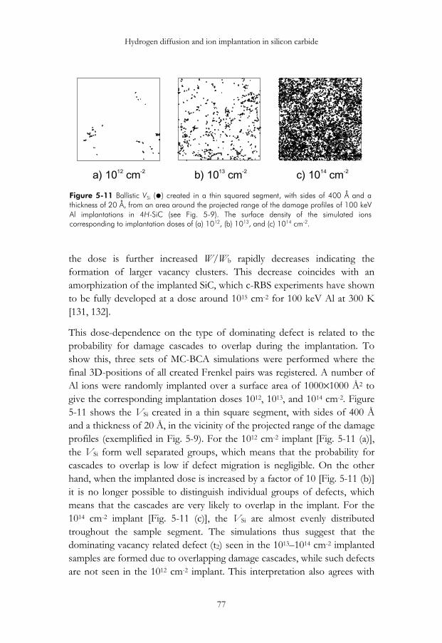
Hydrogen diffusion and ion implantation in silicon carbide
77
the dose is further increased W/Wb rapidly decreases indicating theformation of larger vacancy clusters. This decrease coincides with anamorphization of the implanted SiC, which c-RBS experiments have shownto be fully developed at a dose around 1015 cm-2 for 100 keV Al at 300 K[131, 132].
This dose-dependence on the type of dominating defect is related to theprobability for damage cascades to overlap during the implantation. Toshow this, three sets of MC-BCA simulations were performed where thefinal 3D-positions of all created Frenkel pairs was registered. A number ofAl ions were randomly implanted over a surface area of 1000×1000 Å2 togive the corresponding implantation doses 1012, 1013, and 1014 cm-2. Figure5-11 shows the VSi created in a thin square segment, with sides of 400 Åand a thickness of 20 Å, in the vicinity of the projected range of the damageprofiles (exemplified in Fig. 5-9). For the 1012 cm-2 implant [Fig. 5-11 (a)],the VSi form well separated groups, which means that the probability forcascades to overlap is low if defect migration is negligible. On the otherhand, when the implanted dose is increased by a factor of 10 [Fig. 5-11 (b)]it is no longer possible to distinguish individual groups of defects, whichmeans that the cascades are very likely to overlap in the implant. For the1014 cm-2 implant [Fig. 5-11 (c)], the VSi are almost evenly distributedtroughout the sample segment. The simulations thus suggest that thedominating vacancy related defect (t2) seen in the 1013–1014 cm-2 implantedsamples are formed due to overlapping damage cascades, while such defectsare not seen in the 1012 cm-2 implant. This interpretation also agrees with
a) 10 cm12 -2 b) 10 cm13 -2 c) 10 cm14 -2
Figure 5-11 Ballistic VSi (●) created in a thin squared segment, with sides of 400 Å and athickness of 20 Å, from an area around the projected range of the damage profiles of 100 keVAl implantations in 4H-SiC (see Fig. 5-9). The surface density of the simulated ionscorresponding to implantation doses of (a) 1012, (b) 1013, and (c) 1014 cm-2.

5.3 Ion implantation – damage
78
the identification of t1 as an elementary point defect (VSi) and t2 as acomplex (divacancy).
5.4 Simulation of ion implantationThe access to precise and efficient process simulators has become vital inmodern semiconductor technology in order to decrease the developmenttime and cost for new types of devices. To simulate ion implantations twodifferent approaches can be used depending on the purpose of thesimulation: (i) simulators based on physical models of the ion stoppingprocesses or (ii) a purely statistical approach where the simulated profilesare constructed from a large data bank of experimental distributions. Thelatter type of simulators are based on the fact that most ion range depthprofiles can be represented − to a high degree of accuracy − by their first tofourth order distribution moments, Rp, ∆Rp, γ, and β, using Pearsonfrequency distribution functions [133, Paper VIII]. The main advantage ofthe statistical simulators is the instantaneous execution time. Depth profilesof multiple energy implantations can thus be readily and precisely simulatedby interpolation between established distribution moments, providing thatthe amount of experimental data is sufficient. The usefulness of this type ofsimulation is exemplified in Fig. 5-12, which depicts the SIMS profile of an8-fold multiple energy 11B implantation in SiC together with a simulation ofthe implant using Pearson distributions. The interpolated distributionmoments of the simulated profiles are from Paper VIII. The execution timeof a corresponding simulation using a physically based approach wouldtypically be on the order of several hours.
However, the use of statistical simulators is strictly limited to cases wheresufficient experimental data exists, and it does not provide any informationof the damage profiles or collision events. This can be accomplished bysimulating the stopping process of the implanted ions. There are mainlytwo types of physically based simulators: molecular dynamics (MD)simulations, and simulators based on the binary collision approximation(BCA). The MD algorithm, briefly described in Sec. 5.1.1, is the mostaccurate, but is currently too demanding for studying more than individualion-target interactions. For the normal user, with limited computerresources, simulators based on the BCA approximation are mostly used andare also most often sufficient.

Hydrogen diffusion and ion implantation in silicon carbide
79
In this thesis both statistical and BCA based simulators have been explored.A lengthier description of the former approach is given in Paper VIII, whilethe latter is described in the following section.
5.4.1 Monte-Carlo BCA simulationsIn the following, a relatively detailed description of a simulation algorithmbased on the binary collision approximation is presented. This algorithm isa so-called Monte-Carlo (MC) method, which means that the simulateddistributions are the sum of a large number of individual ion trajectories,each affected by a set of random numbers. An alternative to the MC-BCAmethod are the BCA algorithms employing the Bolzmann transportequations [134]. However, since this method only allows amorphous targetsand since the increasing computer power makes MC-BCA simulationsattainable for the everyday user, it is rarely used nowadays. The first MC-BCA computer programs were presented already in the early 1950s butmost BCA codes of today stem from the algorithms described by Robinsonet al. in the mid 1970s [135, 136], i.e. those implemented in the MARLOWEsimulation code. A few years later Biersack and Haggmark presented thewidely spread TRIM code [137], which was especially designed to decreasethe computer execution time. Other reasons for the popularity of theTRIM package (or SRIM, as it is called today) are the inclusion of anextensive library of empirical stopping data for a large number of ion-target
SIMS profile
Pearson simulatedimplantation distributions:
Individual profiles Multiple profile
Figure 5-12 SIMS (dotted line) andPearson simulated (solid line) depthprofiles of an 8-fold 11B implantationin 4H-SiC, with ion energies rangingfrom 25 to 300 keV. The individualsimulated profiles for each energy areincluded as thin broken lines. Theenergy dependent distributionmoments used in the Pearsonfunctions have been extracted fromPaper VIII.

5.4 Ion implantation – simulation
80
combinations [102], and that it is extremely user friendly. However, one ofthe sacrifices that was made to increase the computer efficiency is thatTRIM can only handle amorphous targets. TRIM has become a more orless standard tool for ion implantation and this has, for example, led to anunderestimation of the range of implantation induced damage in somestudies [138, 139]. Considering the enormous increase in computer powersince TRIM was first developed, this rather severe limitation is no longerneeded. Today there exists many different MC-BCA codes for crystallinetargets, for example MARLOWE, Crystal-TRIM [140], KING-IV [141],and SIIMPL [this thesis], but none of these have been able to match theaccessibility, the user friendliness, and the large empirical data bank ofTRIM. One challenging task for the ion implantation simulationcommunity would be to make simulations of crystalline targets an optionwithin the TRIM package.
Basic principlesThe MC-BCA algorithm is event driven, which in this case means that theion trajectory is determined by consecutive binary collisions, as opposed toMD simulations where the ion path is discretized in time. The event drivenpropagation of a MC-BCA ion trajectory is demonstrated in Fig. 5-13 (a).An ion at position I is heading towards the target atoms A, B, and C. Thetarget atom of the next binary collision is the one which is closest to the ion(projected on the ion velocity vector and in front of it) and that has animpact parameter p which is smaller than a certain maximum value pmax. In
A
∆r
C
B
I
I´
I´´
pmax
p A
A'
B
I
I´
A
A'B
I
I´
(a) (b) (c)
Figure 5-13 Geometry for the subsequent collisions between an ion I and the target atoms A, B,and C in a MC-BCA simulation with a maximum impact parameter of pmax. The target atomsremain at their respective lattice positions in (a) while a random displacement has been added tothe lattice position of A after it has been chosen as a collision partner, bringing A to a position A´that is closer (b) or further away (c) from I.

Hydrogen diffusion and ion implantation in silicon carbide
81
Fig. 5-13 (a) this is atom A since p > pmax for atom C, and B is further awayfrom I than A. The value of pmax should be chosen large enough so thatcollisions with p > pmax have a negligible affect on the ion trajectory, but nottoo large since the number of collisions per unit path length in a simulationincreases as pmax2. Typical values for pmax are 2-3 Å. Once the collisionpartner is found the ion is moved forward a distance ∆r to the asymptoticpoint of the collision I´ (see also Fig. 5-2) and the nuclear kinetic energyloss T, and scattering angles ϑ and φ, are calculated by solving Eq. (5-4)After subtraction of the electronic energy loss (see below) the procedure isrepeated − the next collision in Fig. 5-13 (a) would be with atom B at I´´ −until the ion energy falls below some lower limit value, typically in order ofa few eV, where the ion is considered to be stopped. When simulatingrange distributions, a large number of ions is followed from a randomlychosen position at the target surface until they are stopped. For a targetwith an ideal lattice, i.e. no thermal vibrations or damage, it is only the startposition that involves any random numbers in a simulation.
The bottlenecks of MC-BCA codes are typically the algorithms that searchfor the next collision partner and the solution of the scattering integral, Eq.(5-4a). While earlier codes solved the scattering integral by some time-consuming numerical method, one of the main achievements of the TRIMcode was an effective treatment of the problem, i.e. the so-called MagicFormula [102, 137]. However, with the increasing memory resources ofmodern computers, the scattering integral is fastest solved by employing a2D look-up interpolation scheme [142].
The MC-BCA simulations presented in this thesis have been performedusing a new code for crystalline targets, developed as a part of this work.The program has named SIIMPL (simulation of ion implantation) and inthis version, the scattering integral has been solved using the MagicFormula with the universal interatomic potential [102].
Electronic StoppingThe electronic energy loss is subtracted from the ion energy in eachcollision. This energy loss can either be treated as a conventional stoppingforce, i.e. ∆Ee = NSe∆r, or, as originally proposed by Firsov [106], as afunction of the impact parameter [Eq. (5-7)]. This latter approach ispreferable and physically motivated since experiments have shown that theelectronic stopping is less for channeled ions than for ions with a “random”

5.4 Ion implantation – simulation
82
trajectory. The most commonly used form of an impact parameterdepending electronic stopping is that of Oen and Robinson [136]
∆EeOR = ANSeexp(−sp/a), (5-9)
where s is a constant originally set to 0.3, but is usually treated as a fittingparameter, and a = a(Z1, Z2) is a screening length. A = A(pmax, s, a) is anormalizing constant, which ensures that the average stopping cross sectionof Eq. (5-9) for a random trajectory is equal to Se. The dependence of the sparameter in ∆EeOR on the range profile of a 60 keV Al implantation in the[ 3211 ] direction of 4H-SiC is depicted in Fig. 5-14. One simulation isperformed with no impact parameter dependence (s = 0) , and three with sset to 0.3, 0.5, and 0.7, respectively. All simulations give the same projectedrange for ions that never entered a channel at the surface (the random peakat 0.07 µm), which shows that the normalization parameter A in Eq. (5-9)has been accurately determined. The differences in penetration depth forthe deepest channeled ions are, on the other hand, substantial. The best fitto the experimental profile among these values is given for the simulationwith s set to 0.5.
Figure 5-14 Normalized SIMS profile (thick solid line) of a 60 keV Al implantation into the[1123] direction of 4H-SiC. MC-BCA simulations (histograms) of the implantation with the sparameter of the Oen-Robinson electronic stopping expression set to 0, 0.3, 0.5, and 0.7 arealso included. The mean electronic stopping in the simulations is from paper V.

Hydrogen diffusion and ion implantation in silicon carbide
83
Thermal vibrationsAs already mentioned in Sec. 5.2, thermal vibrations of the target atoms arean important factor for the dechanneling of channeled ions and shouldtherefore be included in MC-BCA simulations of crystalline targets. In theMARLOWE code, vibrations of the atoms are treated in such a way thatthe collision partner is first located assuming a frozen lattice. A random3D-displacement with a Gaussian distributed amplitude and a standarddeviation of 3 <ux> is thereafter added to the lattice position, after whichthe impact parameter and point of collision are recalculated (see Table 2-IIfor typical values of <ux> at 300 K). However, this treatment bringsproblems that may be difficult to circumvent. Figure 5-13 (b) illustrates asituation where the thermal displacement has brought the atom from latticeposition A to a position A’, closer to the ion. This means that if thescattering angle in the collision with A is small, the ion, now at I´, maycollide with atom A a second time. This effect was, however, taken intoaccount and could be avoided [135]. What was not considered is thesituation where the thermal displacement brings the atom further awayfrom the ion [Fig. 5-13 (c)], which also gives rise to severe problems. In thiscase, when the ion is moved to the position I´, there is a probability that thecollision with atom B never occurs, irrespective of the impact parametersfor the collisions. For a channeled ion, i.e. with a trajectory almost parallelto the atomic rows, the probability for this to happen is substantial sincethe projections on the ion path of the lattice positions of two atoms atopposing sides of the channel then can be very close. This is for examplethe case for the atoms A and B in Fig. 5-13.
Unfortunately, there is no easy way to solve this latter problem. Instead, itwould be better to add the displacements to the lattice positions first andthen search for the collision partners. Naturally, the displacements can thennot be extracted using random numbers since they would have to be thesame for the same atom position each time it is evaluated, to avoid theabove mentioned problems. However, by replacing the random numbers bya rapidly − relative to the distance between neighboring atoms − oscillatingfunction that is a function of the laboratory lattice position |r| only,seemingly uncorrelated lattice vibrations can be accomplished. In this waythe problems of the MARLOWE model are avoided since the positions ofthe atoms are not changed after a collision partner has been found.Appendix C presents an effective algorithm that produces these “quasi
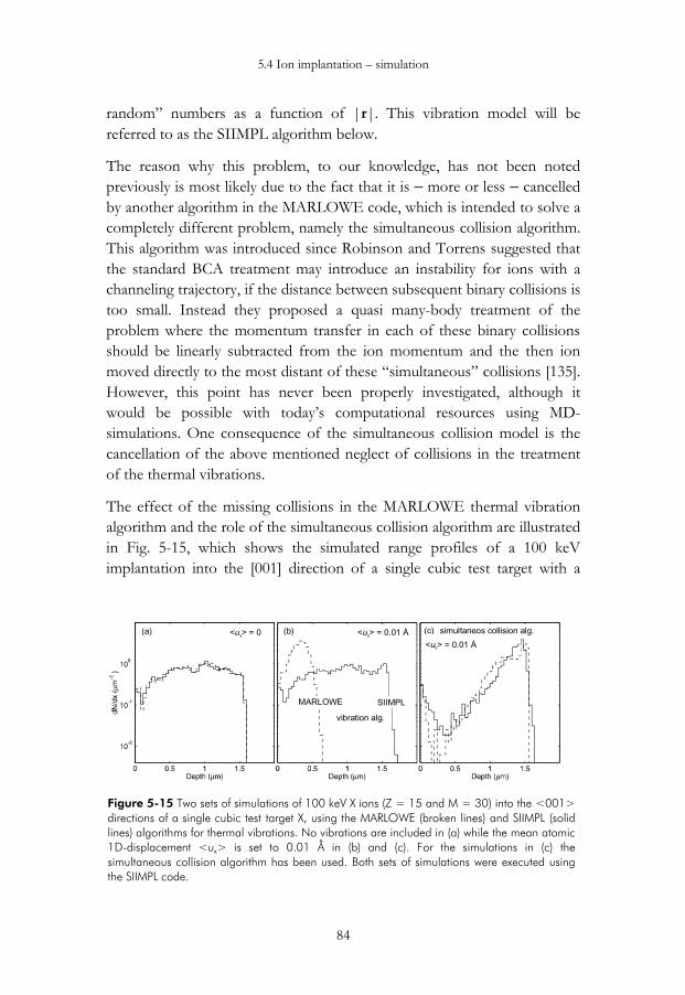
5.4 Ion implantation – simulation
84
random” numbers as a function of |r|. This vibration model will bereferred to as the SIIMPL algorithm below.
The reason why this problem, to our knowledge, has not been notedpreviously is most likely due to the fact that it is − more or less − cancelledby another algorithm in the MARLOWE code, which is intended to solve acompletely different problem, namely the simultaneous collision algorithm.This algorithm was introduced since Robinson and Torrens suggested thatthe standard BCA treatment may introduce an instability for ions with achanneling trajectory, if the distance between subsequent binary collisions istoo small. Instead they proposed a quasi many-body treatment of theproblem where the momentum transfer in each of these binary collisionsshould be linearly subtracted from the ion momentum and the then ionmoved directly to the most distant of these “simultaneous” collisions [135].However, this point has never been properly investigated, although itwould be possible with today’s computational resources using MD-simulations. One consequence of the simultaneous collision model is thecancellation of the above mentioned neglect of collisions in the treatmentof the thermal vibrations.
The effect of the missing collisions in the MARLOWE thermal vibrationalgorithm and the role of the simultaneous collision algorithm are illustratedin Fig. 5-15, which shows the simulated range profiles of a 100 keVimplantation into the [001] direction of a single cubic test target with a
(a) < > = 0ux
< > = 0.01 Åux
simultaneos collision alg.(c)
SIIMPL
vibration alg.
< > = 0.01 Åux(b)
MARLOWE
Figure 5-15 Two sets of simulations of 100 keV X ions (Z = 15 and M = 30) into the <001>directions of a single cubic test target X, using the MARLOWE (broken lines) and SIIMPL (solidlines) algorithms for thermal vibrations. No vibrations are included in (a) while the mean atomic1D-displacement <ux> is set to 0.01 Å in (b) and (c). For the simulations in (c) thesimultaneous collision algorithm has been used. Both sets of simulations were executed usingthe SIIMPL code.

Hydrogen diffusion and ion implantation in silicon carbide
85
lattice parameter of 2 Å. Both the ion and target atoms are of a test speciesX, which has been defined with atomic number 15 and mass 30. Thesimulations using the two different thermal vibration algorithms are bothexecuted using the SIIMPL code. In Fig. 5-15 (a) simulations are performedwith a frozen lattice and the profiles of the MARLOWE and SIIMPLalgorithms are practically identical. However, when a very small vibration isincluded, <ux> = 0.01 Å, [Fig. 5-15 (b)] the simulated profile using theMARLOWE vibration algorithm becomes considerably more shallow,while the SIIMPL profile does not differ significantly from the simulationsof a frozen lattice. The SIIMPL result seems to make more senseconsidering the small amplitude of the vibrations. Figure 5-15 (c) shows thesimulated profiles with the same small lattice vibration as in Fig. 5-15 (b),but now also including the simultaneous collision algorithm in bothsimulations. Again both algorithms produce very similar profiles, but witheven less dechanneling compared to the frozen lattice simulations in Fig. 5-15 (a). These results clearly demonstrate that the MARLOWE treatment ofthermal vibrations leads to a significantly overestimated dechanneling rateand that this artifact is cancelled by the inclusion of the simultaneouscollision algorithm. As a consequence, these results also put some majorquestion marks around the proposed limitations of the BCA treatmentcaused by simultaneous collisions.
Damage and dose dependenceThe calculation of ballistic damage profiles, i.e. of mono vacancies andinterstitials produced in the binary collisions, is a relatively straight forwardprocedure in MC-BCA simulations. If the energy transferred from the ionto the target atom in a collision T exceeds the displacement energy Ed forthat species (see Sec. 5.3), the ion trajectory of the recoiling secondary atomis treated in the same way as the implanted, primary ion. Since there is notime dependence in the MC-BCA scheme and hence no correlationbetween the recoils, the trajectories of the secondary ions and thesubsequent generations of recoils that they may produce, can be performedone at a time after the primary ion trajectory has been completed. Thismethod is usually referred to as the full damage cascade algorithm. Asimpler way to determine damage profiles is the Kinchin-Pease model,which states that the interstitial and vacancy concentration profiles areproportional by a factor of 0.4/Ed to the distribution of energy deposited innuclear collisions by the primary ion [102]. This is a much faster method

5.4 Ion implantation – simulation
86
since the recoiling trajectories are not simulated, but it is less accurateespecially for compound targets. Full damage cascade calculations must alsobe employed to demonstrate effects like the small forward shift of theinterstitial relative to the vacancy profiles [143].
If the crystal damage reaches high enough concentrations during animplantation, the trajectories of the subsequently implanted ions may beseriously affected. This dose-effect can be seen as a saturation ofchanneling tails in ion range profiles, since atoms displaced by theimplantation (in the following called interstitials) gradually “fill” thechannels of the crystal and hence enhance the dechanneling rate. Examplesof this type of dose dependent range profiles in SiC can be found in PapersVI and VII. A simple way to include this phenomenon in MC-BCAsimulations is to evaluate the probability of the next collision to be acollision with an implantation induced interstitial atom. This probability P isoften [140, 144, Paper VI] evaluated as
P = ca NI/N , (5-10)
where NI is the local density of interstitials provided by the simulation. ca isa semi empirical parameter, which among other things includerecombination, clustering, and the scattering efficiency of the point defects.P is then compared to a random number, which decides if the collision is tobe with an interstitial instead of a lattice atom. The collision with aninterstitial atom could in principle be done by defining the position of theinterstitial in the unit-cell, but it is more commonly treated as a collisionwith a randomly positioned target atom. In the MARLOWE code this isaccomplished by a random rotation of the crystal before the collision, whilethe SIIMPL code randomly positions the target atom in a cylinder in frontof the ion, which has a radius pmax and a length Lcyl = 2(πpmax2N)-1. Thesame models can also be used for simulations of amorphous targets oramorphous surface layers.
However, by evaluating P according to Eq. (5-10) the dose dependence forions with a channeling trajectory will not be unambiguously treated in thesimulation, which is explained in the following. Since the interstitial atomsare assumed to be randomly distributed in the target, it follows that theaverage path length between collisions with the interstitial atoms, <∆rI>,should be,

Hydrogen diffusion and ion implantation in silicon carbide
87
<∆rI> = (πpmax2caNI)-1, (5-11)
for all types of ion trajectories. In the BCA simulations, <∆rI> will be givenby
<∆rI> = <∆r> / P , (5-12)
where <∆r> is the average path length between subsequent binary collisionswith the target atoms. For an ion with a random trajectory, <∆r> is givenby
<∆rrand> = (πpmax2N)-1, (5-13)
which shows that the simulated <∆rI> [Eq. (5-12)] for a random path ionbecomes identical to Eq. (5-11) with P evaluated according to Eq. (5-10).However, for an ion with a channeling trajectory, Eq. (5-13) is no longervalid due to the ordered movement of the ion relative the lattice, and <∆rI>will thus differ from the value stipulated by Eq. (5-11). Simulations haveshown that depending on the value of pmax, <∆r> for a channeled ion candiffer up to about 30% compared to <∆rrand>. This has the effect that thedechanneling rate caused by implantation induced damage is over- orunderestimated by the same amount. One way to overcome this problem isto instead evaluate P as:
P = caNI <∆rloc> πpmax2, (5-14)
where <∆rloc> is a local value, determined during the simulation andupdated typically every 50 collisions. In this way, Eq. (5-11) will alwayshold. In SIIMPL P is evaluated according to Eq. (5-14).
Simulation examplesA critical test for a simulation code is to examine its ability to handleimplantations in various high symmetry directions of a crystal. This hasbeen done using the SIIMPL code for the 9 different alignments of thedose-independent 60 keV Al implantations in 4H-SiC, presented earlier inSec. 5.2 and in Paper VII. The simulated and experimental profiles areshown in Fig. 5-16. The labels, (a)-(i), of the panels in Fig. 5-16 correspondto those in Fig. 5-7. Two parameters have been adjusted in thesesimulations: the s parameter of the ∆EeOR expression (Eq. 5-9), and thethickness, La, of an amorphous surface layer. The introduction of this typeof layer is a standard procedure in this kind of simulations [145-148] and

5.4 Ion implantation – simulation
88
has been physically motivated to represent a native oxide on the samplesurface. However, La is usually treated as a fitting parameter in thesimulations in order to obtain a correct channeling fraction. The averageelectronic stopping, Se, is the one extracted in Paper V. The simulatedprofiles are found to be in good agreement with the experimental ones forall directions. This is quite remarkable considering the large variation of theexperimental profiles, which is clearly demonstrated in Fig. 5-6, and the factthat the same set of parameters was used in all simulations to accomplish anoverall best fit, namely s = 0.52 and La = 8 Å.
0 0.5 1 1.5 2 2.5 3
(b) [1120]
0 0.2 0.4 0.6 0.8 1
(a) [0001]
10-3
10-2
10-1
100
101
0 0.5 1 1.5 2 2.5 3
(c) [1123]
(h) 10 off [1120] in (1010) plane
o
0 0.2 0.4 0.6 0.8 110-3
10-2
10-1
100
101 (g) 9 off [0001] in (1010) plane
o
0 0.2 0.4 0.6 0.8 1
(i) 10 off [1120] in plane 55 off (0001)
o
o
0 0.2 0.4 0.6 0.8 1
0 0.2 0.4 0.6 0.8 1
(e) 10 off [1120] in (0001) plane
o
0 0.2 0.4 0.6 0.8 1
(f) 8 off [0001] in plane between (1010) and
(1120)
o
10-3
10-2
10-1
100
101
0 0.2 0.4 0.6 0.8 1
(d) 8 off [0001] in (1120) plane
o
Depth (µm)
Con
cent
ratio
n ( a
rb. u
nits
)
Figure 5-16 Normalized SIMS (solid lines) and MC-BCA simulated (histograms) profiles ofnine 60 keV Al implantations in different axial (a-c), planar (d-e, g-h), and low symmetry (f, i)directions of 4H-SiC (see paper VII for experimental details). The simulations are performedusing SIIMPL with the s parameter in the Oen-Robinson electronic stopping model set to 0.52,and with an amorphous surface layer of 8 Å thickness to obtain an overall best fit for allsimulations. The average Se is the one determined in Paper V.

Hydrogen diffusion and ion implantation in silicon carbide
89
Figure 5-17 shows the simulated dose dependence for the above described60 keV Al implantations in the [0001] and [ 3211 ] axial directions of 4H-SiC, where ca has been adjusted to obtain best possible fits to theexperimental SIMS profiles. These simulations use slightly different valuesof s and La than those above, to give the best possible fit for the dose-independent profiles in each direction. For the [0001] implants of Fig. 5-17(a), ca was set to 0.6. This value is interestingly enough very close to thevalue obtained for a 1.5 MeV Al implantation in the [0001] direction of 6H-SiC, using a different MC-BCA code [Paper VI]. For the [ 3211 ] implants,on the other hand, best fits were obtained using ca = 0.25 [Fig. 5-17 (b)].This difference in observed in the extracted ca parameters may be caused bythe fact that the interstitial defects are not randomly distributed, as assumedin the simulations, but have fixed positions in the lattice and thereforeaffect the ions differently in different crystal channels. It may therefore bepossible to gain information of the position of the defects in the crystalfrom this type of profiles, using a more refined model for the interstitialtype defects in the simulations.
0 0.2 0.4 0.6 0.8 1 1.2 1.4 1.6 1.8 20 0.2 0.4 0.61015
1016
1017
1018
1019(a) [0001] (b) [1123]
Depth (µm)
Con
c ent
r atio
n (c
m)
-3
Figure 5-17 SIMS (solid lines) and MC-BCA simulated (histograms) profiles of 60 keV Alimplantations in the [0001] (a) and [1123] (b) axial directions of 4H-SiC (see Paper VII forexperimental details). The dose dependence was accounted for in the simulations with the ca
parameter of the random scattering model set to 0.6 and 0.25 for the [0001] and [1123]implantations, respectively.

6. Summary of results
90
6 Summary of results
The main body of the results presented in this summary stem from theappended articles, but some results refer to co-authored papers that havenot been included in this thesis (Refs. [86], [149], and [150]) and topreviously unpublished results presented in the preceding chapters.
Hydrogen (H) has been found to form electrically neutral complexes withthe acceptors B and Al in SiC [149, 150]. By studying the redistribution ofH during thermal anneals in a large number of pre-hydrogenated samples, acomprehensive understanding of the formation and dissociation kinetics ofthese complexes have been obtained. An effective capture radius for theformation of 2H-B complexes at 460 °C has been determined to RHB = (21±4) Å [Paper I]. This value is in good agreement with that expected for aCoulomb force assisted trapping mechanism. Furthermore, the dissociationenergies, Ed, for the two complexes have been determined and the largedifference between the extracted values, (2.51 ±0.04) eV for 2H-B and (1.61±0.02) eV for 2H-Al, suggested that the atomic configurations of the twocomplexes are significantly different [Paper I]. This conclusion was latersupported in an ab-initio computational study by Aradi et al. [93], who alsoquantitatively reproduced the observed difference in Ed between the twocomplexes.
The migration of H under a reverse bias Schottky contact has revealed thatH is present as H+ in p-type SiC [86]. By studying the H redistribution insamples containing large doping gradients, the influence of internal electricfields on the H migration could be revealed [Papers II-III]. It wasdemonstrated that drift of H+ has to be accounted for when gradients inthe doping profile are present, although the original intention to use thiseffect to determine the intrinsic H diffusion constant was not successful(see Sec. 4.2.2). On the other hand, the effect of the built-in electric fieldson the H migration was exploited in another experiment to reveal thatpractically 100% of the mobile H are in the positive charge state in p-typeacceptor doped material [Sec. 4.2.2]. This result also agreed with the ab initiopredicted position of the negative-U (+/−) level for H in the upper half ofthe 4H-SiC band gap [93].

Hydrogen diffusion and ion implantation in silicon carbide
91
The first published one of the appended papers, Paper IV, presents a studyof the out-diffusion of implanted 2H during thermal anneals attemperatures ≥1000 °C. It was found that the amount of implanted 2Hdecreased according to first order kinetics, and that the depth profiles couldbe well represented by computer simulations assuming trapping anddetrapping of mobile H at implantation induced defects. A dissociationenergy for the process of ~5 eV was extracted and the trapping centerswere tentatively assigned to a Si-vacancy, VSi.
A large number of “random” direction implantations of 1H up to 75As havebeen performed at energies ranging from a few keV up to several MeV. Theimplantations were analyzed by SIMS and the first to fourth orderdistribution moments of the range profiles were determined. Withadditional range data obtained from the literature a vast library ofimplantation range distributions in SiC was assembled. In Paper V, this dataare used to extract the low velocity electronic stopping cross sections, Se,for 1H, 2H, 7Li, 11B, 14N, 16O, 27Al, and 31P. It was found that the Se
behavior in SiC is in good qualitative agreement with the low-velocity Se
behavior previously reported in carbon. This includes the so-called Z1-oscillations (Z1 = ion atomic number) and the energy dependence of thestopping, which was found to be smaller than the square root (i.e. smallerthan being proportional to the ion velocity) for ions with Z1 ≤ 8. The mainimportance of the results presented in Paper V is perhaps that it presentsstopping data which can be used in various implantation simulators to giveaccurate predictions for ion implantation in SiC. The range data were alsoused, in Paper VIII, to create an empirical implantation simulator for SiC,using Pearson frequency functions. This was accomplish by fittinganalytical functions to the extracted distribution moments as a function ofimplantation energy, which then could be used as a compact look-upscheme for an implantation of a certain energy.
A series of implantations in high symmetry directions of 4H- and 6H-SiChas also been performed to study the effect of ion channeling as a functionof implantation direction, dose, ion mass, and energy. The results presentedin Papers VI and VII can be used as a guide in the choice of tilt angles forSiC wafers during implantation in order to minimize the channeling effect,but serves primarily the purpose as standards for atomistic simulationmodels of ion implantation. By fitting simulated implantation profiles to thedepth profiles of these aligned implantations, detailed information about

6. Summary of results
92
electronic stopping and damage accumulation can be extracted [Papers VIand VII, and Sec. 5.4.1].
A new Monte-Carlo binary collision approximation simulation code for ionimplantation in crystalline targets has been developed. The code is namedSIIMPL (simulation of ion implantation) and include several updatedalgorithms, as partly described in Sec. 5.4.1. The SIIMPL code has beenemployed for the results presented in Papers V, VII, VIII, and IX.Simulations of the implantations performed in Paper VII are furtherpresented in Sec. 5.4.1. It should be noted, however, that the simulationspresented in Paper VI were performed using another MC-BCA code.
The last of the appended papers, Paper IX, presents a study where PASmeasurements have been undertaken to study the vacancy type defectdistributions of 11B-, 14N-, and 27Al-implanted 4H-SiC. The Doppler-broadening line-shape parameters of two types of radiation induced pointdefects were established and tentatively identified as VSi and VCVSi (seealso Sec. 3.2.5). Paper IX further demonstrates that the implantationinduced defects detected by PAS at considerably greater depths than themean projected range of the implanted ions, Rp, were primarily caused byion-channeling during the implantations. This effect has previously beenreported by other groups for SiC and also for other implanted materials,but it was not concluded whether it was caused by diffusion ofimplantation-induced defects from the region around Rp, or, as shown inPaper IX, by deeply channeled ions.
Hydrogen diffusion and ion implantation in silicon carbide
93
AcknowledgementsFirst of all I would like to express my gratitude towards my supervisorAnders Hallén. He had the difficult task of keeping me on reasonable trackduring this sometimes bumpy journey, and also to direct me back to earthwhen needed. I am also greatly in debt to my co-supervisor MargaretaLinnarsson for patiently introducing me to the SIMS technique and foreveryday discussions. Bengt Svensson has a great responsibility for theexistence of this thesis. It was his inspiring lecturing in a solid state theorycourse (a course I was later to teach in) that first brought my attention tothis research field, and it was also Bengt who accepted me as a Ph.D.student at the FTE laboratory. Bengt is further acknowledged fornumerous interesting discussions and for his always careful proof readingof my manuscripts.
Experimental physics is to a high degree a collective effort. This thesis is agood illustration of this, considering that the appended papers are authoredby a total of 12 people. This number increases to an astonishing figure of62 when the authors of the papers that were not included in this thesis arealso counted. All of my co-authors are greatly acknowledged, but I wouldlike to send special thanks to Jonatan Slotte at the Helsinki University ofTechnology (HUT), especially for his patient understanding regarding thedifficulties we encounter with the implantations for the PAS experiments.Furthermore, I am also most grateful to Jennifer Wong-Leung for being aterrific host and for enduring the impossible work-load I laid upon herduring my stay at the Australian National University in Canberra (ANU).
Many of the experiments presented in this thesis would not have beenpossible without the unique epitaxially grown SiC structures, which weresupplied by Nils Nordell, Stefan Karlsson, Adolf Schöner, and AndreyKonstantinov. Thank you all. Furthermore, I am also grateful to ErikDanielsson and to my room-mate, Uwe Zimmermann, for their assistancewith the ICP etchings. Uwe is also highly appreciated for, among manythings, his proof reading of this thesis and for putting up with my musicover the past five years.

Acknowledgements
94
The FTE laboratory (now MSP) has been an inspiring place to work at. Ithas especially been a privilege to work in such an internationalenvironment; individuals from 18 different nations have been part of theFTE staff ever since I fist started my masters project, 6 years ago. All ofyou are greatly acknowledged for contributing to the relaxed atmosphere atFTE.
Finally, I would like to direct my gratitude to Ulf Karlsson for his activeconcerns regarding my academic future on the other side of this thesis.
The work presented in this thesis has been supported by the SiliconCarbide Electronics Program (SiCEP) of the Swedish Foundation forStrategic Research (SSF). My visit at HUT was financed by the NordicAcademy for Advanced Study (NorFA), while my stay at ANU wassponsored by the Swedish Foundation for International Cooperation inResearch (STINT). Part of the costs for the conference trips was coveredby the scholarships from the Generaldirektör Waldemar Borgquist, Sten och LisaVelander, and E.C. Ericsson foundations.
Martin Janson
Stockholm, February 2003

Hydrogen diffusion and ion implantation in silicon carbide
95
Appendix A: Solution of the positrontransport equation at steady state
This appendix outlines a precise and computer efficient method to solvethe 1D positron transport differential equation at steady state,
( ) 0=+−−−��
���
��++ pddf ICCCCE
dxd
dxdCD
dxd
dbµ
τµ , (A1)
where D+ is the positron diffusivity, C the concentration of positrons atposition x, µ+ the positron mobility in an electric field Ef, τb the positronbulk lifetime, Cd the concentration of positron trapping centers withtrapping coefficients µd, and IP the positron generation (implantation) term.
The solution generally follows the one published by van Veen et al. for theVEPFIT code [54], but since an attempt to implement their solution failed− most likely due to some printing error in Table 2 of Ref. [54] − a correcttreatment is given in the following. This solution also permits gradients inthe electric field, which was not allowed in the one given by van Veen et al.
Formulation of problemIntroducing Einstein’s relation for the mobility, µ+ = D+eEf/kBT, where e isthe elementary charge, kB the Bolzmann constant, and T the absolutetemperature, and assuming a constant D+, Eq. (A1) may be rewritten as
γβα −=−− CdxdC
dxCd2
2, (A2)
α = eEf / (kBT),
β = ( ΣµdCd + 1/τb ) / D+ + dEf/dx (e/kBT),
γ = I / D+ .
Note that the last term in the β expression has been omitted in theVEPFIT code [54], which will generate an erroneous solution in thepresence gradients in the electric field.
Two boundary conditions for the surface (x = x0) are considered. The firstcondition assumes that the surface acts as a perfect sink for the positrons:

Appendix A: Solution of the positron transport equation at steady state
96
Cx = x0 = 0 (A3)
The second type is a so-called radiative boundary condition that states thatthe flux J is proportional, by a factor −Λ, to the concentration of positronsat the surface
Jx = x0 = −Λ C, (A4a)
which, including diffusion and drift, at the surface can be written as
dC/dxx = x0 = (α + Λ/D+) C . (A4b)
The surface boundary condition is usually treated as a fitting parameterwhen simulating a SPB measurement. The deep boundary (x = xN) shouldbe chosen deep enough so that I ≈ Ef ≈ 0 and Cd = Cd x = xN for x > xN. Inthat case the deep boundary condition can be written [54]
dC/dxx = xN = − Cβ (A5)
Numerical solutionThe problem is discretized into N segments between x0 and xN so that theapproximation∇α = ∇β = ∇γ = 0 can be made in each slab. Equation (A2)can then be solved for each slab i
Ci(x) = Ai exp(di+x) + Bi exp(di
-x) + γi /βi (A6)
with di± = iii βαα +± 4/2/ 2 . The 2N coefficients Ai and Bi are
determined by enforcing continuity for the neighboring Ci(x) and dCi/dx(x), and with the boundary conditions of Eqs. (A3) − (A5). Introducing thevariables ci = Ci (x = xi) and ci´ = dCi/dx (x = xi) the problem can bereformulated as
Mc = b, (A7)
where M is a tri-diagonal matrix of size N×N, and c and b are vectors oflength N.

Hydrogen diffusion and ion implantation in silicon carbide
97
The elements of M and b are given in Table A1. ci´ can be determined oncec has been solved from Eq. (A7):
ci´ = ( ci-1 – fici – gi) / ei ( i = 2 .. N) (A8a)
c1´ = e2´ c2´ + f2´c2 + g2´ (A8b)
where ei, ei´, fi, fi´, gi, and gi´ are defined in Table A-I. Once Eq. (A7) hasbeen solved Ai and Bi in Eq. (A6) may be determined from the ci and ci´elements.
TABLE A-ITABLE A-ITABLE A-ITABLE A-I. Elements of matrix MMMM and vector bbbb in equation McMcMcMc = bbbb where cccc are the discretizedpositron concentrations at xi, ci = Cx = xi .
i mi,i-1 mi,i mi,i+1 bi
2 .. N − 1 -1/ei1
1´
+
++i
i
i
iee
ef
11
11
´´ ++
++ − i
i
ii f
eef
i
ii e
gl −
1(Cx = x0 = 0) - ↑ ↑ ↑
1(Jx = x0 = −ΛC) -
2
2
101
101 ´´´
ee
eLefLf
+−−
↑101
1011 ´
´eLegLg
l−−
−
N -1NNN ef β− - - gN
L0 = (α0 + Λ/D+)-1, 111
1 ´´++
+
+ −= iii
ii gg
eel
−+
−+
−−=
ii
iii
ddhhe , −+
+−−+
−−=
ii
iiiii
ddhdhdf ,
i
i
ii
iiiii
dd
hdhdddg ii
βγ
−+
+−−+−+
−
+−−= ,
−+
−−++
−−=
ii
iiiii
ddhdhde , ( )
−+
−++−
−−=
ii
iiiii
ddddhhf ´ , ( )
i
i
ii
iiiii
ddddhhg
βγ
−+
−+−+
−−=´ ,
( )1−± −−± = iii xxd
ih e , ii
iid β
αα +±=±42
2

Appendix B: Steady-state H profiles in the presence of doping gradients and trapping
98
Appendix B: Steady-state H profiles in thepresence of doping gradients and trapping
In the presence of an internal electric field, E(x), generated by gradients inthe doping profile, the steady-state concentration of mobile H+ is nothomogeneous. This is realized by setting ∂[H+]/∂t = 0 in Eq. (4-7) (with A≡ H+), which gives the steady state solution for H+, relative to the H+
concentration at some point x0, as
[ ][ ]
( )���
�
�
���
�
�
= �+
+ x
xBx
x dxxETk
q
00
´´expH
H(B-1)
It can be seen that this ratio follows the corresponding ratio for holes andthe ratio of [H+] between two points x1 and x2 − where the local dopinggradient is negligible − will therefore follow the ratio of the uncompensatedand non-passivated ionized acceptors, −
AN :
[ ][ ]
2
1
2
1
xA
xA
x
x
N
N−
−
+
+
=H
H. (B-2)
When the acceptor, X, that gives rise to the built-in electric field also is themain trapping center for the mobile H+, the concentration of H-Xcomplexes at steady-state [Eq. (4-8)],
[ ] [ ][ ]+= HXH
HXυ
πRD4, (B-3)
will not be directly proportional to the acceptor concentration, whichwould be anticipated if the H concentration is homogenous. Instead aquadratic dependence on [X] is expected. For a system where [H]tot ≈ [HX],i.e. [H+] << [HX], and with −
AN = [X] = X0 – [HX] – [H+] = X0 – [H]tot,Eqs. (B-2) and (B-3) give the total concentration of H at equilibrium
[ ] [ ]( )2tot0tot HH −= Xk , (B-4)
where X0 is the total, chemical concentration of the acceptor atom, and k isa proportionality constant. In Eq. (B-4) it has also been assumed that [H+]<< X0 – [Htot]. This is always true when [H+] << [HX] except for the case

Hydrogen diffusion and ion implantation in silicon carbide
99
of saturation trapping, where [HX] = X0. For the case where [Htot] << X0,the measured total H concentration will exhibit a pure quadraticdependence on the acceptor concentration.
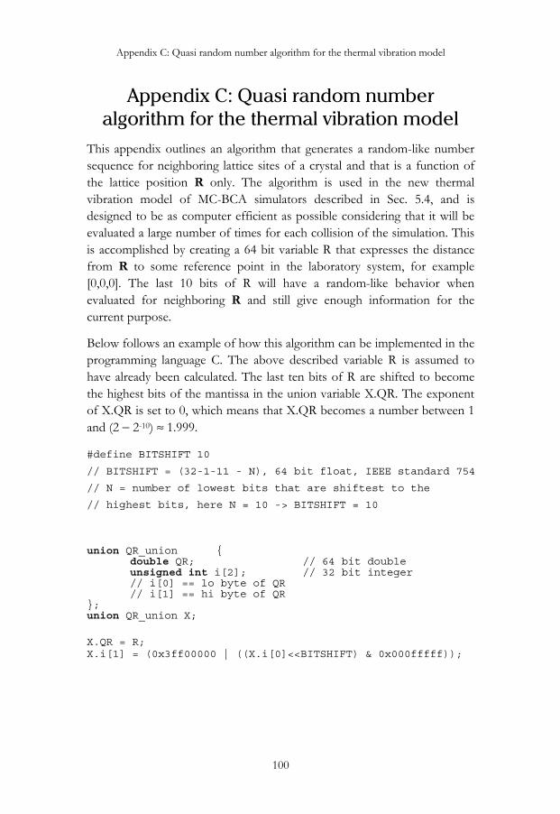
Appendix C: Quasi random number algorithm for the thermal vibration model
100
Appendix C: Quasi random numberalgorithm for the thermal vibration model
This appendix outlines an algorithm that generates a random-like numbersequence for neighboring lattice sites of a crystal and that is a function ofthe lattice position R only. The algorithm is used in the new thermalvibration model of MC-BCA simulators described in Sec. 5.4, and isdesigned to be as computer efficient as possible considering that it will beevaluated a large number of times for each collision of the simulation. Thisis accomplished by creating a 64 bit variable R that expresses the distancefrom R to some reference point in the laboratory system, for example[0,0,0]. The last 10 bits of R will have a random-like behavior whenevaluated for neighboring R and still give enough information for thecurrent purpose.
Below follows an example of how this algorithm can be implemented in theprogramming language C. The above described variable R is assumed tohave already been calculated. The last ten bits of R are shifted to becomethe highest bits of the mantissa in the union variable X.QR. The exponentof X.QR is set to 0, which means that X.QR becomes a number between 1and (2 − 2-10) ≈ 1.999.
#define BITSHIFT 10
// BITSHIFT = (32-1-11 - N), 64 bit float, IEEE standard 754
// N = number of lowest bits that are shiftest to the
// highest bits, here N = 10 -> BITSHIFT = 10
union QR_union {double QR; // 64 bit doubleunsigned int i[2]; // 32 bit integer// i[0] == lo byte of QR// i[1] == hi byte of QR
};union QR_union X;
X.QR = R;X.i[1] = (0x3ff00000 | ((X.i[0]<<BITSHIFT) & 0x000fffff));

Hydrogen diffusion and ion implantation in silicon carbide
101
References[1] A. G. Acheson, Engl. Pat. 17911 (1892).[2] R. Siegele, S. P. Withrow, J. Roth, and B. M. U. Scherzer, J. Nucl. Mat. 176-177,1010 (1990).[3] M. Mehregany and C. A. Zorman, Thin solid films 355-356, 518 (1999).[4] H.J. Round, Electrical World 19, 309 (1907).[5] S. J. Pearton, J. W. Corbett, and M. Stavola, Hydrogen in crystalline semiconductors(Springer-Verlag, New York, 1991).[6] J. I. Pankove and N. M. Johnson, Hydrogen in semiconductors (Academic Press,New York, 1991).[7] N. Nordell, A. Schöner, and S. G. Andersson, J. Electrochem. Soc. 143, 2910(1996).[8] D. J. Larkin, S. G. Sridhara, and W. J. Choyke, J. Electr. Mat. 24, 289 (1995).[9] A. Schöner, K. Rottner, N. Nordell, M. K. Linnarsson, C. Peppermüller, and R.Helbig, Diamond and Rel. Mater. 6, 1293 (1997).[10] J. Portman, C. Haug, R. Brenn, J. Schneider, K. Rottner, and R. Helbig, Nucl.Instr. Meth. Phys. Res. B 155, 132 (1999).[11] M. K. Linnarsson, U. Forsberg, M. S. Janson, E. Janzén, and B. G. Svensson,Mater. Sci. Forum 389-393, 565 (Trans Tech Publ., Switzerland, 2002)[12] G. Pensl and R. Helbig, Festkörperprobleme 30, 133 (1990).[13] C. H. Park, B.-H. Cheong, K.-H. Lee, and K. J. Chang, Phys. Rev. B 49, 4485(1994).[14] W. J. Choyke and G. Pensl, MRS Bulletin 22, 25 (1997).[15] G. L. Harris, Properties of silicon carbide (INSPEC, IEE, 1995).[16] W. Kaindl, M. Lades, N. Kamenski, E. Miemann, and G. Washutka,J. Elechtrochem. Mater. 28, 154 (1999).[17] E. N. Mokhov, E. E. Goncharov, and G. G. Ryabova, Sov. Phys. Semicond.18, 27 (1984).[18] A. Zywietz, K. Karch, and F. Bechstedt, Phys. Rev. B 54, 1791 (1995).[19] D. S. Gemmel, Rev. Mod. Phys. 46, 129 (1974).[20] Semiconductors: Physics Of Group IV Elements and III-V Compounds, Landholt-Börnstein, New Series III Vol. 17a, edited by O. Madelung, M. Schulz, and H.Weiss, (Springer-Verlag, Berlin, 1982)[21] D. G. Clerc, J. Mater. Sci. Lett. 17, 1461 (1998).[22] C. Kittel, Introduction to solid state physics (John Wiley & Sons, Inc., New York,1996).[23] M. A. Capano, J. J.A. Cooper, M. R. Melloch, A. Saxler, and W. C. Mitchel, J.Appl. Phys. 87, 8773 (2000).

References
102
[24] C. Raynaud, C. Richier, P. N. Brounkov, F. Ducroquet, G. Guillot, L. M.Porter, R. F. Davis, C. Jaussaud, and T. Billon, Mater. Sci. Eng. B 29, 122 (1995).[25] T. Troffer, C. Peppermüller, G. Pensl, K. Rottner, and A. Schöner, J. Appl.Phys. 80, 3739 (1996).[26] D. J. Larkin, Phys. Stat. Sol. (b) 202, 305 (1997).[27] S. G. Sridhara, L. L. Cleman, R. P. Devaty, W. J. Choyke, D. J. Larkin, H. S.Kong, T. Troffer, and G. Pensl, J. Appl. Phys. 83, 7909 (1998).[28] T. Troffer, M. Schadt, T. Frank, H. Itoh, G. Pensl, J. Heindl, H. P. Strunk, andM. Maier, Phys. Stat. Sol. A 162, 277 (1997).[29] N. Nordell, A. Schöner, and M. K. Linnarsson, J. Electr. Mat. 26, 187 (1997).[30] M. K. Linnarsson, M. S. Janson, U. Zimmermann, B. G. Svensson, P. O. Å.Persson, L. Hultman, J. Wong-Leung, S. Karlsson, A. Schöner, H. Bleichner, andE. Olsson, Appl. Phys. Lett. 79, 2016 (2001).[31] M. K. Linnarsson, M. S. Janson, A. Schöner, and B. G. Svensson, Mater. Res.Soc. Symp. 742, MRS fall meeting in Boston, Dec. 2002, (accepted)[32] Y. A. Vodakov and E. N. Mokhov, in Int. Conf. on SiC, edited by R. C.Marshall, J. J.W. Faust and C. E. Ryan, (Univ. of South Caroline Press, 1973),p. 508.[33] M. A. Capano, S. Ryu, M. R. Melloch, J. J.A. Cooper, and M. R. Buss, J. Electr.Mat. 27, 370 (1998).[34] Y. Gao, I. Soloviev, and T. S. Sudarshan, J. Appl. Phys. 90, 5647 (2001).[35] T. Kimoto, N. Miyamoto, A. Schöner, A. Saitoh, K. Asano, and Y. Sugawara,J. Appl. Phys. 91, 4242 (2002).[36] T. Kimoto, A. Itoh, H. Matsunami, T. Nakata, and M. Watanabe, J. Electr.Mat. 25, 879 (1996).[37] S. Seshadri, G. W. Eldridge, and A. K. Agarwal, Appl. Phys. Lett. 72, 2026(1998).[38] J. N. Pan, J. J.A. Cooper, and M. R. Melloch, J. Electrochem. Mater. 26, 208(1997).[39] H. Lendemann, A. Mukhitdinov, F. Dahlquist, H. Bleichner, M. Irwin, R.Söderholm, and P. Skytt, Proc of 13th International Symposium on Power SemiconductorDevices & ICs. IPSD '01, (Inst. Electr. Eng. Japan, 2001).[40] P. O. Å. Persson, L. Hultman, M. S. Janson, A. Hallén, R. Yakimova, D.Panknin, and W. Skorupa, J. Appl. Phys 92, 2501 (2002).[41] H. Wirth, D. Panknin, W. Skorupa, and E. Niemann, Appl. Phys. Lett. 74, 979(1999).[42] E. Kalinina, G. Kholujanov, V. Solov'ev, A. Strel'chuk, A. Zubrilov, V.Kossov, R. Yafaev, A. P. Kovarski, A. Hallén, A. Konstantinov, S. Karlsson, C.Adås, S. Rendakova, and V. Dmitriev, Appl. Phys. Lett. 77, 3051–3053 (2000).[43] K. S. Woodcock, Phys. Rev. 38, 1696 (1931).[44] H. J. Liebl and F. K. Herzog, J. Appl. Phys. 34, 2893 (1963).

Hydrogen diffusion and ion implantation in silicon carbide
103
[45] R. F. K. Herzog, W. P. Poschenrieder, and F. G. Satkiewicz, Nasa, ContractNo. NAS 5-9254, NASA CR-683 (1969).[46] P. Sigmund, Phys. Rev. 184, 383 (1969).[47] P. C. Zalm, Vacuum 45, 753 (1994).[48] M. K. Linnarsson and B. G. Svensson, Phys. Rev. B 60, 14302 (1999).[49] M. S. Janson, M. K. Linnarsson, A. Henry, B. Magnusson, A. Hallén, and B.G. Svensson, To be published .[50] M. S. Janson, M. K. Linnarsson, J. Wong-Leung, and A. Hallén, To bepublished .[51] A. Kawasuso, F. Redmann, R. Krause-Rehberg, T. Frank, M. Weidner, G.Pensl, P. Sperr, and H. Itoh, J. Appl. Phys. 90, 3377 (2001).[52] R. Krause-Rehberg and H. S. Leipner, Positron annihilation in semiconductors(Springer-Verlag, Berlin, 1999).[53] J. Gebauer, S. Eichler, R. Krause-Rehberg, and H. P. Zeindl, Appl. Surf. Sci.116, 247 (1997).[54] A. v. Veen, H. Schut, J. d. Vries, R. A. Hakvoort, and M. R. IJpma, in 4th Inter.Workshop on Slow-Positron Beam Tech. for Solids and Surfaces, AIP Conf. Proc. 218, p.171.[55] S. Dannefaer, C. Craigen, and D. Kerr, Phys. Rev. B 51, 1928 (1995).[56] G. Brauer, W. Anwand, P. G. Coleman, A. P. Knights, F. Plazola, Y. Pacaud,W. Skorupa, J. Störmer, and P. Willutzki, Phys. Rev. B 54, 3084 (1996).[57] S. Arpiainen, K. Saarinen, P. Hautojärvi, L. Henry, M.-F. Barthe, and C.Corbel, Phys. Rev. B 66, 075206 (2002); S and W data from private communicationwith K. Saarinen[58] A. Polity, S. Hulth, and M. Lausmann, Phys. Rev. B 59, 10603 (1999).[59] W. Puff, A. G. Balogh, and P. Mascher, Mater. Sci. Forum 338-342 (TransTech Publ., Swizerland, 2000), p. 969.[60] T. E. M. Staab, L. M. Torpo, M. J. Puska, and R. M. Nieminen, Mater. Sci.Forum 353-356 (Trans. Tech. Publ, Switzerland, 2001), p. 533.[61] K. Saarinen, P. Hautojärvi, and C. Corbel, in Identification of Defects inSemiconductors, edited by M. Stavola (Academic, New York, 1998, 1998), p. 209.[62] G. Brauer, W. Anwand, P. G. Coleman, J. Stormer, F. Plazaola, J. M. Campillo,Y. Pacaud, and W. Skorupa, J. Phys: Cond. Mat. 10, 1147 (1998).[63] C. D. Beling, S. Fung, S. H. Cheng, M. Gong, C. C. Ling, Y. F. Hu, and G.Brauer, Mater. Sci. Forum. 255-257, 260 (1997).[64] A. Uedono, H. Itoh, T. Ohshima, R. Suzuki, T. Ohdaira, S. Tanigawa, Y. Aoki,M. Yoshikawa, I. Nashiyama, T. Mikado, H. Okumura, and S. Yoshida, Jpn. J.Appl. Phys. 36, 6650 (1997).[65] H. Itoh, A. Uedono, T. Ohshima, Y. Aoki, M. Yoshikawa, I. Nashiyama, S.Tanigawa, H. Okumura, and S. Yoshida, Appl. Phys. A 65, 315 (1997).

References
104
[66] M.-F. Barthe, L. Henry, C. Corbel, G. Blondiaux, K. Saarinen, P. Hautojärvi,E. Hugonnard, L. D. Cioccio, F. Letertre, and B. Ghyselen, Phys. Rev. B 62, 16638(2000).[67] A. Uedono, S. Tanigawa, T. Ohshima, H. Itoh, M. Yoshikawa, I. Nashiyama,T. Frank, G. Pensl, R. Suzuki, T. Ohdaira, and T. Mikado, J. Appl. Phys. 87, 4119(2000).[68] B. K. Panda, G. Brauer, W. Skorupa, and J. Kuriplach, Phys. Rev. B. 61, 15848(2000).[69] A. A. Rempel, K. Blaurock, K. J. Reichle, W. Sprengel, and H.-E. Schaefer,Mater. Sci. Forum 389-393 (Trans Tech Publ., Switzerland, 2002), p. 485.[70] A. Kawasuso, H. Itoh, M. Yoshiwaka, T. Ohshima, I. Nashiyama, S. Okada, H.Okumura, and S. Yoshida, Appl. Phys. A 67, 209 (1998).[71] W. Puff, A. G. Balogh, and P. Mascher, in Inter. Conf. on SiC and Rel. Mat. 1999,edited by J. C. H. Carter, R. P. Devaty and G. S. Roher, Mat. Sci. Forum338-342(Trans Tech Publ., Swizerland, 2000), p. 965.[72] A. Uedono, T. Ohshima, H. Itoh, R. Suzuki, T. Ohdaira, S. Tanigawa, Y. Aoki,M. Yoshikawa, and T. Mikdo, Jpn. J. Appl. Phys 37, 2422 (1998).[73] A. I. Girka, A. D. Mokrushin, E. N. Mokhov, S. V. Svirida, and A. V. Shishkin,Mater. Sci. Froum 105-110 (1992).[74] C. C. Ling, D. Beling, and S. Fung, Phys. Rev. B 62, 8016 (2000).[75] L. Torpo, T. E. M. Staab, and R. M. Nieminen, Phys. Rev. B 65, 085202(2002).[76] G. Brauer, W. Anwand, E. M. Nicht, J. Kuriplach, M. Sob, N. Wagner, P. G.Coleman, M. J. Puska, and T. Korhonen, Phys. Rev. B 54, 2512 (1996).[77] C.-T. Sah, J. Y.-C. Sun, and J. J.-T. Tzou, Appl. Phys. Lett. 43, 201 (1983).[78] J. I. Pankove, D. E. Carlson, J. E. Berkeyheiser, and R. O. Wance, Phy. Rev.Lett. 51, 2224 (1983).[79] J. I. Pankove, P. J. Zanzucchi, C. W. Magee, and G. Lucovsky, Appl. Phys.Lett. 46, 421 (1985).[80] G. G. DeLeo and W. B. Fowler, Phys. Rev. B 31, 6861 (1985).[81] T. R. Wait, J. Chem. Phys. 28, 103 (1958).[82] J. J. Thomson, Philos. Mag. 47, 337 (1924).[83] B. K. Ridley, Quantum Processes in Semiconductors (Oxford University Press, 1993).[84] C. H. Seager, R. A. Anderson, and D. K. Brice, J. Appl. Phys. 68, 3268 (1990).[85] T. Zundel and J. Weber, Phys. Rev. B 39, 13 549 (1989).[86] N. Achtziger, C.Hülsen, W. Witthuhn, M. K. Linnarsson, M. Janson, and B. G.Svensson, Phys. Stat. Sol (b) 210, 395 (1998).[87] T. Zundel and J. Weber, Phys. Rev. B 46, 2071 (1992).[88] S. J. Pearton, C. R. Abernathy, and J. Lopata, Appl. Phys. Lett. 59, 3571(1991).

Hydrogen diffusion and ion implantation in silicon carbide
105
[89] W. Pfeiffer, M. Diecher, R. Keller, R. Mayerk, E. Recknagel, H. Skudlik, T.Wichert, H. Wolf, D. Forkel, N. Moriya, and R. Kalish, Appl .Phys. Lett 58 (1991).[90] M. C. Wagener, J. R. Botha, and A. W. R. Leicht, Phys. Rev. B 62, 15315(2000).[91] R. Rahbi, B. Pajot, J. Chevallier, A. Marbeuf, R. C. Logan, and M. Gavand, J.Appl. Phys. 73, 1723 (1993).[92] R. Bouanani-Rahbi, B. Pajot, C. P. Ewels, S. Öberg, J. Goss, R. Jones, Y.Nissim, B. Theys, and C. Blaauw, in 7th International Conference on Shallow-LevelCenters in Semiconductors, edited by C. A. J. Ammerlaan and B. Pajot, (WorldScientific, Singapore, 1997), p. 171.[93] B. Aradi, A. Gali, P. Deák, N. T. Son, and E. Janzén, Physica B 308-310, 722(2001).[94] P. Deák, A. Gali, and B. Aradi, J. Phys: Condens. Matter 13, 9019 (2001).[95] A. Fick, Ann. Phys. (Leipzig) 170, 59 (1855).[96] A. J. Tavendale, D. Alexiev, and A. A. Williams, Appl. Phys. Lett. 47, 316(1985).[97] A. J. Tavendale, S. J. Pearton, and A. A. Williams, Appl. Phys. Lett. 56, 949(1990).[98] J. Zhu, N. M. Johnson, and C. Herring, Phys. Rev. B 41, 12353 (1990).[99] C. G. VandeWalle, P. J. H. Denteneer, Y. Bar-Yam, and S.T.Pantalides, Phys.Rev. B 39, 10791 (1989).[100] L. Pavesi and P. Giannozzi, Phys. Rev. B 46, 4621–4629 (1992).[101] J. Neugebauer and C. G. VandeWalle, Phys. Rev. Lett. 75, 4452 (1995).[102] J. F. Ziegler, J. P. Biersack, and Y. Littmark, The stopping and range of ions insolids (Pergamon press, 1985).[103] J. J. Thomson, Conduction of Electricity Through Gases (Cambridge Univ. Press,1903).[104] J. Lindhard and M. Scharff, Phys. Rev. 124, 128 (1961).[105] I. S. Tilinin, Phys. Rev. A 51, 3058 (1995).[106] O. B. Firsov, Sov. Phys. JETP 36, 1076 (1959).[107] P. M. Echenique, R. M. Nieminen, J. C. Ashley, and R. H. Ritchie, Phys. Rev.A 33, 897 (1986).[108] J.H. Ormrud and H.E. Duckworth, Can. J. Phys. 41, 1424 (1963); J.H.Ormrud, J.R. Macdonald, and H.E. Duckworth, Can. J. Phys. 43, 275 (1965)[109] P. Hvelplund and B. Fasterup, Phys. Rev. 165, 408 (1968).[110] P. Sigmund, Nucl. Instr. and Meth. B 135, 1 (1998).[111] D. Ward, H. R. Andrews, I. V. Mitchell, W. N. Lennard, R. B. Walker, and N.Rud, Can. J. Phys. 57, 645 (1979).[112] D. G. Simons, D. J. Land, J. G. Brennan, and M. D. Brown, Phys. Rev. A 12,2383 (1975).

References
106
[113] D. J. Land, J. G. Brennan, D. G. Simons, and M. D. Brown, Phys. Rev. A 16,492 (1977).[114] K. B. Winterbon, Can. J. Phys. 46, 2429 (1968).[115] S. A. C. C. Vargas and D. K. Brice, Nucl. Instr. Meth. Phys. Res. B 170, 205(1980).[116] H. Bethe, Ann. Phys. (Leipzig) 5, 324 (1930).[117] F. Bloch, Ann. Phys. (Leipzig) 16, 285 (1933).[118] W. Brandt and M. Kitagawa, Phys. Rev. B 25, 5631 (1982).[119] P. Sigmund, Phys. Rev. A 56, 3781 (1997).[120] J. Lindhard, K. Dan. Vidensk. Selsk. Mat.-Fys. Medd. 34 (1965).[121] S. M. Sze, VLSI technology (McGraw-Hill Book Company, New York, 1988).[122] Cree Inc., www.cree.com, (2003).[123] Sterling Semiconductor, www.sterling-semiconductor.com, (2003).[124] E. Morvan, N. Mestres, F. J. Campos, J. Pascual, A. Hallén, M. Linnarsson,and A. Y. Kuznetsov, Mater. Sci. Forum 338-342 (Trans Tech Publ., Switzerland,2000), p. 893.[125] T. D. d. l. Rubia, R. S. Averback, R. Benedek, and W. E. King, Phys. Rev.Lett. 59, 1930 (1987).[126] K. Nordlund, J. Keinonen, M. Ghaly, and R. S. Averback, Nature 398, 49(1999).[127] S. J. Zinklea and C. Kinoshitab, J. Nucl. Mater. 251, 200 (1997).[128] R. Devanathan, W. J. Weber, and F. Gao, J. Appl. Phys. 90, 2303 (2001).[129] L. Malerba and J. M. Perlado, Phys. Rev. B 65, 045202 (2002).[130] A. Hallén, N. Keskitalo, and B. G. Svensson, Defect and diffusion Forum153-155, 193 (1998).[131] A. Y. Kuznetsov, M. S. Janson, A. Hallén, B. G. Svensson, C. Jagadish, H.Grünleitner, and G. Pensl, Mater. Sci. Forum 353-356, 595 (2001).[132] A. Hallén, M. S. Janson, A. Y. Kuznetsov, D. Åberg, M. K. Linnarsson, B. G.Svensson, P. O. Å. Persson, F. H. C. Carlsson, L. Storasta, J. P. Bergman, S. G.Sridhara, and Y. Zhang, Nucl. Instr. and Meth. in Phys. Res. B 186, 186 (2002).[133] D. G. Ashworth, R. Oven, and B. Mundin, J. Phys, D 23, 870 (1990).[134] P. Sigmund, Phys. Scripta 28, 257 (1983).[135] M. T. Robinson and I. M. Torrens, Phys. Rev. B 9, 5008 (1974).[136] O. S. Oen and M. T. Robinson, Nucl. Instr. Meth. Phys. Res. 132, 647 (1976).[137] J. P. Biersack and L. G. Haggmark, Nucl. Instr. Meth. Phys. Res. 174, 257(1980).[138] M. Fujinami and N. B. Chilton, J. Appl. Phys. 73, 3242 (1993).[139] A. Nylandsted-Larsen, C. Christensen, and J. W. Petersen, J. Appl. Phys. 86,4861 (1999).

Hydrogen diffusion and ion implantation in silicon carbide
107
[140] M. Posselt, B. Schmidt, T. Feudel, and N. Strecker, Mat. Sci. and Eng. B 71,128 (2000).[141] G. Lulli, E. Albertazzi, M. Bianconi, and R. Nipoti, Nucl. Instr. Meth. Phys.Res. B 148, 573 (1999).[142] B. Yuan, F. C. Yu, and S. M. Tang, Nucl. Instr. Meth. Phys. Res. B 83 (1993).[143] P. Lévêque, H. K. Nielsen, P. Pellegrino, A. Hallén, B. G. Svensson, A. Y.Kuznetsov, J. Wong-Leung, C. Jagadish, and V. Privitera, J. Appl. Phys. 93, 871(2003).[144] G. Lulli, E. Albertazzi, M. Biancola, R. Nipoti, M. Cervera, A. Carnera, andC. Cellini, J. Appl . Phys. 82, 5958 (1997).[145] E. H. A. Dekempeneer, P. C. Zalm, G. v. Hoften, and J. Politiek, Nucl. Instr.Meth. Phys. Res. B 48, 224 (1990).
[146] M. Posselt, B. Schmidt, C. S. Murthy, T. Feudel, and K. Suzuki,J. Electrochem. Soc. 144 1495 (1997)[147] D. Cai, C. M. Snell, K. M. Beardmore, and N. Gronbech-Jensen, Internat. J.Mod. Phys. C 9, 459 (1998).[148] S.-H. -. Yang, S. J. Morris, S. Tian, K. B. Parab, and A. F. T. Jr., IEEE Trans.Semicond. Manufacturing 9, 49 (1996).[149] M. K. Linnarsson, M. Janson, A. Schöner, N. Nordell, S. Karlsson, and B. G.Svensson, Mater. Sci. Forum 264-268 761 (Trans Tech Publ., Switzerland, 1998)[150] N. Achtziger, J. Grillenberger, W. Witthuhn, M. K. Linnarsson, M. Janson,and B. G. Svensson, Appl. Phys. Lett. 73, 945 (1998).