hybrid superconducting nanostructures: very low ... · hybridsuperconductingnanostructures 457...
TRANSCRIPT

HAL Id: hal-00954424https://hal.archives-ouvertes.fr/hal-00954424
Submitted on 4 Mar 2014
HAL is a multi-disciplinary open accessarchive for the deposit and dissemination of sci-entific research documents, whether they are pub-lished or not. The documents may come fromteaching and research institutions in France orabroad, or from public or private research centers.
L’archive ouverte pluridisciplinaire HAL, estdestinée au dépôt et à la diffusion de documentsscientifiques de niveau recherche, publiés ou non,émanant des établissements d’enseignement et derecherche français ou étrangers, des laboratoirespublics ou privés.
Hybrid superconducting nanostructures: very lowtemperature local probing and noise
Claude Chapelier, F. Lefloch, Hervé Courtois, Klaus Hasselbach
To cite this version:Claude Chapelier, F. Lefloch, Hervé Courtois, Klaus Hasselbach. Hybrid superconducting nanos-tructures: very low temperature local probing and noise. International Journal of Nanotechnology,Inderscience, 2010, 7, pp.456. <hal-00954424>

456 Int. J. Nanotechnol., Vol. 7, Nos. 4/5/6/7/8, 2010
Hybrid superconducting nanostructures: very lowtemperature local probing and noise
C. Chapelier and F. Lefloch
INAC-SPSMS,CEA Grenoble,17 avenue des martyrs, 38042 Grenoble, FranceE-mail: [email protected]: [email protected]
H. Courtois* and K. Hasselbach
Institut Néel,CNRS and Université Joseph Fourier,25 avenue des martyrs, 38042 Grenoble, FranceE-mail: [email protected]: [email protected]*Corresponding author
Abstract: We review the topic of hybrid superconducting nanostructures
by introducing the basic physical concepts and describing recent key
experimental results. We discuss the superconductivity nucleation in
mesoscopic structures, the vortex lattice imaging in doped diamond
films, the superconducting proximity effect, multiple Andreev reflection
in Josephson junctions and the electronic micro-cooling in hybrid tunnel
junctions. An emphasis is put on very low temperature local probes and
noise measurement techniques developed in Grenoble.
Keywords: near-field microscopy; tunnelling; vortex; micro-cooling;
mesoscopic superconductivity; Andreev reflection; noise.
Reference to this paper should be made as follows: Chapelier, C.,
Lefloch, F., Courtois, H. and Hasselbach, K. (2010) ‘Hybrid
superconducting nanostructures: very low temperature local probing and
noise’, Int. J. Nanotechnol., Vol. 7, Nos. 4/5/6/7/8, pp.456–473.
Biographical notes: Claude Chapelier is a staff member at CEA-Grenoble.
His PhD Thesis (1989) focused on phonons in superfluid helium. Then,
he worked in CNRS (Grenoble) where he has been involved in Mesoscopic
Physics and Persistent currents in normal metal rings. In 1993 and
1994, he designed and built a low temperature UHV STM in Lawrence
Berkeley Laboratory (USA). Since 1995, he developed a very low
temperature STM in CEA-Grenoble. His recent research activities deal
with STM spectroscopy of non-uniform superconducting systems such
as highly disordered superconducting thin films, hybrid superconducting
nanostructures and magnetic vortex in type II superconducting films.
Copyright © 2010 Inderscience Enterprises Ltd.

Hybrid superconducting nanostructures 457
François Lefloch is engineer-physicist at the CEA-Grenoble-INAC inthe Service of Statistical Physics, Magnetism and Superconductivity(SPSMS). After a PhD at CEA-Saclay (spin glass dynamics) and two yearspost-doc at UCLA (NRM response and vortex motion), he reachedthe CEA-Grenoble in 1995. His main research activity focuses on noisemeasurements in multi-terminal superconducting hybrid nanostructuresand more generally in quantum electronic transport in nanostructures.Since 2006, he is the deputy head of the SPSMS.
Hervé Courtois is Professor at Université Joseph Fourier (UJF) since2005 and member of the Institut Universitaire de France. His researchactivity at Institut Néel – CNRS and UJF covers the proximity effectsbetween metals and superconductors, Josephson junctions and electroniccooling. This has led him to develop innovative very low-temperature localprobe microscopes (STM and combined AFM-STM). Since 2005, he is thedirector of the European School On Nanosciences and Nanotechnologies(ESONN, www.esonn.fr).
Klaus Hasselbach is Director of Research (CNRS), PhD UniversityKarlsruhe 1991, Germany, World Trade Post-doctoral Fellow at IBMT.J. Watson Research Lab, 1992. His research activities concernnanomagnetism, superconductivity and scanning probe microscopy.He has developed a novel scanning nano- SQUID microscope working atvery low temperature.
1 Introduction
Superconductivity is a macroscopic quantum state, whose signature is zerodc-resistance and complete diamagnetism. Diamagnetism is achieved by screeningcurrents at the surface of the sample nulling the applied field in thesample (Meissner-Ochsenfeld effect). Superconductivity sets in upon lowering oftemperature as the formation of pairs of electrons allows to diminish theirenergy. The pairs of electrons are called Cooper pairs and consist of twoundistinguishable electrons of opposite spin and momentum. Two length scalescharacterise superconductivity, first the coherence length, ξ, a length correspondingto the spatial extent of a Cooper pair and the penetration depth, λ, the width thesuperconducting screening currents need to shield the field. When a magnetic fieldis applied to a superconductor, it interferes in many ways with superconductivity.The quantum state wavefunction acquires a phase factor, via the vector potential A,resulting in a space-dependent free energy Ginzburg-Landau functional. If theratio of λ/ξ is smaller than 1/
√2, a coexistence of normal and superconducting
regions is observed. The regions have typically length scales of several micrometres,these materials are called type I superconductors and are mostly elementalsuperconductors. If the ratio λ/ξ is larger than 1/
√2, it is energetically favourable
for the material to admit magnetic flux in a quantised manner. These flux quantaare called vortices and contain a flux Φ0 = h/2e = 2.06 × 10⁻¹⁵ Wb with h beingPlanck’s constant and e the charge of the electron. At its centre in a region ofdiameter of ξ, each vortex contains unpaired electrons. When the field rises above

458 C. Chapelier et al.
a first critical field Hc1, vortices begin to penetrate the centre of the sample andsuperconductivity weakens. Due to a repulsive interaction between them, the vorticesarrange themselves in a triangular array (Abrikosov array) which can be more orless distorded depending on the density of pinning centres created by chemical orstructural disorder in the material. Superconductivity disappears in the bulk whenthe vortices cores overlap at a field Hc2, and also from the surface sheath at afield Hc3 = 1.7 Hc2. Between Hc2 and Hc3, the superconducting sheath has a typicalwidth of the order of the coherence length [1]. The superconductivity vanishes lastand appears first at the surface, due to the wavefunction’s boundary condition ofzero transverse amplitude at this place.
When a superconductor is in contact with a normal metal, single electrons aretransformed in Cooper pairs and vice versa continuously. At the N/S interface, themicroscopic mechanism is the Andreev reflection of an electron into a hole, whichtraces back almost exactly the trajectory of the incident electron. This coherentprocess corresponds to the transfer of a Cooper pair in S and its inverse to thediffusion of an electron Andreev pair in the normal metal [2]. In the vicinity ofthe interface, the diffusion of Andreev pairs induces superconducting-like physicalproperties in the normal metal. One aspect of this so-called proximity effect is thelocal modification of the energy spectrum. In the case of a N/S junction with anormal metal of finite length, the density of states in N is expected to exhibit amini-gap: the density of states is zero within an energy window around the Fermilevel. The width of this mini-gap is smaller than the intrinsic superconducting gapof the superconductor. In the case of a normal metal with an infinite length, thedensity of states will exhibit a pseudo-gap: the density of states is zero only atthe exact Fermi level and goes approximately linearly with the energy close tothe Fermi level. This behaviour can be understood by arguing that some electrontrajectories travelling close to the interface never hit it, therefore do not couple tosuperconductivity and contribute to the density of states. Practically, the criteria ofan infinite length for the normal metal should be understood as a length larger thanthe phase coherence length. In every case, the characteristic energy scale is given bythe Thouless energy ETh = !D/L2 where D is the diffusion coefficient and L is thesize of the metal or the distance from the interface.
If two superconductors are connected to a short normal metal (S/N/Sjunction) [3], a dissipationless supercurrent can flow. Here, we consider a lengthof the normal bridge smaller than the phase coherence length Lφ of the normalmetal and transparent contacts between the superconducting electrodes and thenormal metal. A case of particular interest deals with long junctions defined by ajunction length L larger than the induced superconducting coherence length in thenormal metal ξN but still smaller than the single particle coherence length Lφ, incontrast with the short junction case L < ξN met for instance in superconductingatomic point-contacts. In a long S/N/S junction, the Thouless energy ETh =!D/L2 is smaller than the gap ∆ and it determines the amplitude of the maximumsupercurrent. At finite voltage, the charge transport though a S/N/S junction occursmainly through Multiple Andreev Reflections (MAR): normal metal quasiparticleswith an energy ε < ∆ go through successive Andreev reflections at the two N/Sinterfaces until they reach the superconducting gap energy ∆. With an appliedbias V , the number of successive MAR is equal to 2∆/eV + 1. Thus, two regimescan be met depending on the voltage bias. At low bias, the electron and holetrajectories coincide and multiple charge quanta are coherently transferred through

Hybrid superconducting nanostructures 459
the S/N/S junction. In the (high-bias) incoherent regime eV > ETh, the electronand the hole have, away from the interface, independent trajectories. The electronictransport then occurs by incoherent MAR, which induce excess noise as comparedto a similar N/N/N system.
2 Superconductivity nucleation in mesoscopic structures
Two experimental set-ups described below, Scanning Tunnelling Microscopy (STM)and Scanning nano-SQUID Microscopy (SnSM), can probe, in different ways,inhomogeneous superconducting states, such as the mixed state of a type IIsuperconductor. In the case of STM, this is the signature in the LDOS of the zeroingof the order parameter which is probed whereas in the case of SnSM, this is thelocal magnetic field.
2.1 Magnetic microscopy
As an applied magnetic field induces a modulation of the superconducting stateand notably the appearance of vortices, magnetic microscopy is a tool of choiceto observe the inhomogeneous magnetic state of a superconductor. One way to dothis is to scan a microscopic flux meter above the surface of the superconductor.A very sensitive flux-meter is the Superconducting Quantum Interference Device(SQUID). The direct current (dc)-SQUID consists of a superconducting loop withtwo Josephson junctions.
When a magnetic flux Φ threads this superconducting loop, a circularsupercurrent is induced which is periodic with Φ with a period equal to Φ0. Thepresence of such a supercurrent decreases the maximal dissipationless dc-current onecan drive across the SQUID. As a result, this critical current Ic is also a Φ0-periodicfunction of the applied magnetic flux. The measurement of Ic(Φ, x, y) for eachposition (x, y) of the nanoSQUID above the sample surface gives a direct accessto the local variations of the magnetic field. For instance, for a SQUID loop areaof 1 µm2 a periodic modulation of Ic corresponds to a field variation of 2.06 mT.Such a nanoSQUID is well suited for detecting the magnetic field of a vortex in atype II superconducting film in the mixed state. Indeed, such a field can be estimatedas H ≈ Φ0/2πλ2 ≈ 30 mT for a penetration depth λ of the order 100 nm. Howeverthis is an upper limit of H , since it rapidly decreases when one moves away fromthe surface.
We have chosen to aim at high spatial magnetic resolution and adopted thenanoSQUID design based on Dayem bridges as Josephson junctions patterned byelectron beam lithography see Figure 1 [4]. The bridges have a width of the order of20 nm. Microscopes based on bigger and more sensitive SQUID [5] are described inliterature, though their spatial resolution is lesser and their design far more complex.At a height of 1 µm above the surface, the field is reduced to about 1% of theestimated field in the centre of the sample. This rapid decrease of the field amplitudeas a function of the distance between the nanoSQUID and the sample surface meansthat close proximity between sample surface and nanoSQUID has to be maintained.We have chosen to implement an active height regulation between the sample andthe nanoSQUID tip in attaching the nanoSQUID on a piezoelectric Quartz tuning

460 C. Chapelier et al.
fork [6], see Figure 1. As the tuning fork is excited by a dither piezo ceramic, itsresonance frequency which depends on the sample-SQUID distance is tracked bya phase locked loop controller. Any frequency shift is then used in a feedbackloop to maintain this distance constant while scanning, in a similar way as in forcemicroscopy. Such a scanning nanoSQUID force microscope has been integrated ina reversed dilution refrigerator, allowing imaging at very low temperatures.
Figure 1 Left: SEM image of a nanoSQUID of 1 µm diameter made of Aluminum, thetwo Josephson junctions are realised by 20 nm wide Dayem Bridges. Centre:The nanoSQUID placed at the very edge of the Si chip, Right: The sensor of theSQUID force microscope, tuning fork assembled with the nanoSQUID chip
The strength of low temperature high resolution magnetic imaging relies onthe possibility to follow in situ the evolution of the magnetic structure of asuperconductor upon changes in temperature and field. We applied this approachto the study of the vortex arrangements in a patterned array of holes in analuminium film [7]. We chose aluminium because of its long coherence length andin consequence the weak vortex pinning effects. Aluminium behaves as a type-IIsuperconductor if the thickness of the film is of the order of the penetration depth,and if the lateral dimensions are much larger than the thickness. The holes werearranged in a repetitive pattern of lines and each line was made of holes of either 0.5,1 or 1.5 µm diameter. The distance between the holes was 10 µm. Upon cooling in anapplied field, due to the boundary conditions of the superconducting wave-function,the first regions that become superconducting are the regions at the borders of thesample and of the holes. When the edge of an hole becomes superconducting, thewave-function must be 2π periodic around the hole. As a consequence, the fluxthrough the hole is quantised in 1, 2, or 3 Φ0, the quantification being possible due tocirculating screening currents in the superconductor around the holes. Figure 2(b) istaken at a field of 0.2 G, which is the matching field so that each hole carries exactlyone flux quantum. The temperature at a given field for which the surface of each holebecomes superconducting depends on the hole curvature. The smaller the curvature,the closer the temperature gets to the bulk critical temperature. This size dependenceis clearly visible in Figure 2(c). Upon field cooling, the flux passes through thebigger holes and the screening currents are set up to establish the 2π periodicity ofthe wavefunction around these holes. If no flux is left over, no screening currentswill appear when the smaller holes become superconducting at lower temperatures.In this image, the site of the smallest hole remain dark: there are no screeningcurrents.

Hybrid superconducting nanostructures 461
Figure 2 Left: the film is patterned by holes of three diameters 0.5, 1 and 1.5 µm, each10 µm apart, on the images the holes of identical diameter are aligned ondiagonals. Centre: scanning NanoSQUID Microscopy (SnSM) image28 µm × 28 µm with 0.2 G field cooled to 0.4 K. Screening currents appear ateach hole, 0.2 G is the amplitude of the first matching field. Right: SnSM image28 µm × 28 µm with 0.14 G field cooled to 1.16 K. The diagonal of the smallestholes stays void of flux (superconducting regions are dark) (see online versionfor colours)
When the film is cooled in an applied field higher than the first matching field,interstitial vortices appear between the holes, as in Figure 3(a) where the field was1.14 G. These ‘Abrikosov’ vortices nucleate preferentially at defects bigger than thevortex coherence length and stay more or less pinned at their position, as long asthe coherence length stays shorter than the defect size. When the sample is warmedup close to Tc, here 1.18 K, the coherence length in Al starts to diverge and thevortices become mobile, see Figure 3(b). At the same time, the penetration depth λ
diverges also and the vortices become magnetically larger and the repulsion betweenthe vortices diminishes. In Figure 3(b), it becomes apparent that the interstitialvortices are pushed together by the screening currents that circulate around theholes. In average, each vortex cloud between the holes is constituted of fourvortices. When the temperature is raised even more, a new state appears. Localisedsuperconductivity is visible around the larger holes of 1 and 1.5 µm diameter, thesuperconducting surface sheath persists above Hc2 as it is governed by Hc3(r) [8],r being the curvature of the hole, Figure 3(c). This is the first direct observation byan imaging technique of the state of localised superconductivity.
Figure 3 (a) Scanning NanoSQUID Microscopy (SnSM) image 28 µm × 28 µm fieldcooled to 0.4 K at 1.14 G. Interstitial Abrikosov vortices and the vortices due tothe screening currents around the holes are undistinguishable; (b) at 1.18 K theinterstitial Abrikosov vortices become mobile and caged in groups of about4 vortices by the screening currents around the holes and (c) at 1.2 K the regionaround the diagonal of the smallest holes is filled by flux (bright: normal state),the circular regions around the larger holes are still superconducting (dark),which is an evidence for localised superconductivity (see online versionfor colours)

462 C. Chapelier et al.
2.2 STM at low temperature
Scanning Tunnelling Microscopy (STM) provides highly resolved images of surfaces,making individual atoms visible. It can also provide a local spectroscopy of theelectronic properties of nano-objects with atomic scale resolution. The Grenoblevery low temperature STMs work at about 60 mK in a dilution refrigerator [9]. Theyfeature both an atomic resolution and a large scanning range of 6 × 6 µm2 at lowtemperature. In the experiments described in this paper, the cryogenic environmentis not only necessary because superconductivity and quantum coherence innanostructures take place at very low temperature but also because the energyresolution in spectroscopy techniques, such as Scanning Tunnelling Spectroscopy(STS), improves when approaching zero temperature. In this limit, the tunnellingprobability of an electron between the STM tip and the sample is simplyproportional to the local electron density of states (LDOS) of the two materialsintegrated in a energy window eV , the energy shift of the Fermi levels of the twometals. In this energy range, all the electronic states which are fully occupied in oneelectrode can tunnel in fully empty states in the other one. The tunnelling currentcan therefore be written as
I(V ) = GT
∫ eV
0
νt(ε − eV ) νs(ε) dε, (1)
where νt(ε) and νs(ε) are the LDOS of the tip and the sample respectively and GT
a quantity proportional to the tunnelling conductance. Since characteristic energiesfor spectroscopy on superconducting samples at low temperature are in the meVrange, one can assume further a constant LDOS for the tip when made from anormal metal. Then the differential tunnelling conductance becomes proportional tothe LDOS of the sample at an energy eV :
dI
dV= GT e νt(0) νs(eV ). (2)
However, at non-zero temperature, the Fermi-Dirac distribution f(E) influences thetunnelling current, which becomes temperature dependent.
I(V ) = GT νt(0)
∫ +∞
−∞
νs(ε) [f(ε) − f(ε − eV )] dε (3)
and
dI
dV= GT e νt(0)
∫ +∞
−∞
νs(ε)∂f
∂Edε. (4)
In the spectroscopy mode, the energy resolution of a tunnelling experiment is thusgiven by the thermal energy: 3.5 kBT. Our STMs have shown an energy resolutionbelow 36 µeV. One way to improve this resolution is to use a superconducting tipwhose LDOS is peaked at the superconducting gap energy and acts as an additionalenergy filter.
The first picture of an Abrikosov array by STS has been obtained onNbSe2 [10,11]. Moreover, since this material is a clean superconductor (l % ξ, where
Hybrid superconducting nanostructures 463
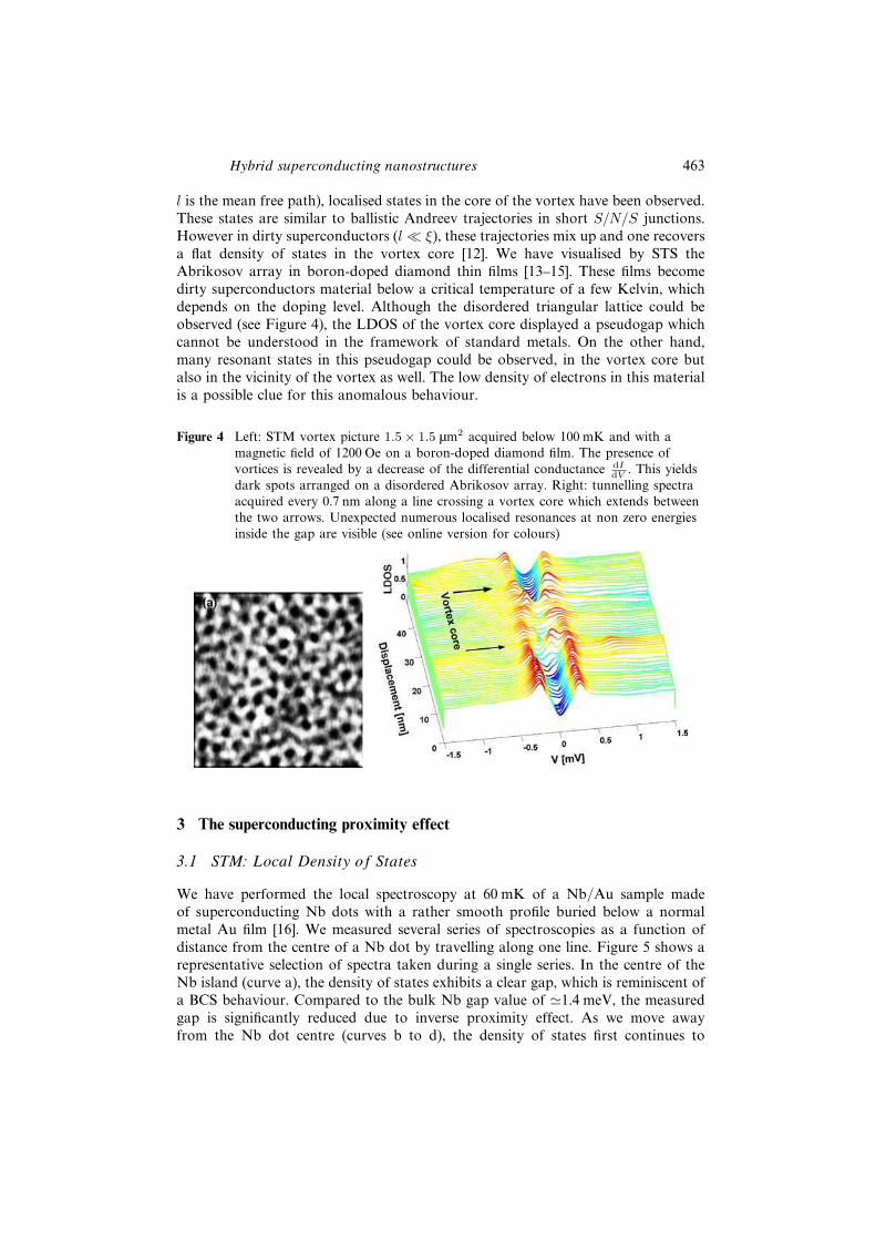
l is the mean free path), localised states in the core of the vortex have been observed.These states are similar to ballistic Andreev trajectories in short S/N/S junctions.However in dirty superconductors (l & ξ), these trajectories mix up and one recoversa flat density of states in the vortex core [12]. We have visualised by STS theAbrikosov array in boron-doped diamond thin films [13–15]. These films becomedirty superconductors material below a critical temperature of a few Kelvin, whichdepends on the doping level. Although the disordered triangular lattice could beobserved (see Figure 4), the LDOS of the vortex core displayed a pseudogap whichcannot be understood in the framework of standard metals. On the other hand,many resonant states in this pseudogap could be observed, in the vortex core butalso in the vicinity of the vortex as well. The low density of electrons in this materialis a possible clue for this anomalous behaviour.
Figure 4 Left: STM vortex picture 1.5 × 1.5 µm2 acquired below 100 mK and with amagnetic field of 1200 Oe on a boron-doped diamond film. The presence ofvortices is revealed by a decrease of the differential conductance dI
dV. This yields
dark spots arranged on a disordered Abrikosov array. Right: tunnelling spectraacquired every 0.7 nm along a line crossing a vortex core which extends betweenthe two arrows. Unexpected numerous localised resonances at non zero energiesinside the gap are visible (see online version for colours)
3 The superconducting proximity effect
3.1 STM: Local Density of States
We have performed the local spectroscopy at 60 mK of a Nb/Au sample madeof superconducting Nb dots with a rather smooth profile buried below a normalmetal Au film [16]. We measured several series of spectroscopies as a function ofdistance from the centre of a Nb dot by travelling along one line. Figure 5 shows arepresentative selection of spectra taken during a single series. In the centre of theNb island (curve a), the density of states exhibits a clear gap, which is reminiscent ofa BCS behaviour. Compared to the bulk Nb gap value of '1.4 meV, the measuredgap is significantly reduced due to inverse proximity effect. As we move awayfrom the Nb dot centre (curves b to d), the density of states first continues to

464 C. Chapelier et al.
exhibit a fully developed but reduced gap. This remains approximately true up toclose to the curve e, which shows a clear pseudo-gap: the density of states goesapproximately linearly to zero at the Fermi level. As the tip is moved further away(spectra e to j), the pseudo-gap width is reduced. We have been able to observea pseudo-gap behaviour in the density of states spectra over about 300 nm. Thisexperimental data compares favourably with the spectra calculated from the Usadelequations [16], assuming a very simple geometrical model of the complex samplegeometry. In the bilayer region, we consider the sample as a bilayer with a varyingNb layer thickness. In the ‘proximity’ region, we consider a lateral N/S junction.From the fit parameters, we found that spin-flip and inelastic scattering could beneglected, which means that the related characteristic lengths should be larger thanabout 300 nm.
Figure 5 Right, top : 2.6 × 5 µm2 STM image at 60 mK captured with a 10 mV biasvoltage and a 30 pA tunnel current. Two circular Nb dots are visible. Right,bottom: profile of the sample surface extracted from image (line indicatedindicated by the arrow) together with a schematics of the sample geometry.Note that the vertical scale has been expanded by a factor of about 10 comparedto the horizontal one. The locations where the spectra were measured areindicated, as well as the domains of application of the two geometry models usedin the calculations. Left: experimental spectra measured on locations a to jduring a single scan along one line (see online version for colours)
We have carried out a similar study in Nb/Au bilayers with an increased gap thanksto a larger thickness of the Nb layer [17]. This increased ∆/kBT enabled us to unveilan anomalous behaviour of the local density of states at the surface: a non-zerodensity of states appears within the mini-gap and increases when the thickness ofthe Au layer is increased. This behaviour is presumably related to the shape of theAu Fermi surface.
3.2 Noise in S/N/S diffusive hybrid superconducting nanostructures
In this section, we describe recent results obtained on the noise in diffusive S/N/Sjunctions. We have measured the current noise of junctions of various length from0.4 µm to 0.8 µm. They are all based on aluminium – copper – aluminium contacts
Hybrid superconducting nanostructures 465
evaporated in situ through shadow masks. This ensures a very good electricalcontact between the superconducting material (Al) and the diffusive metal (Cu).
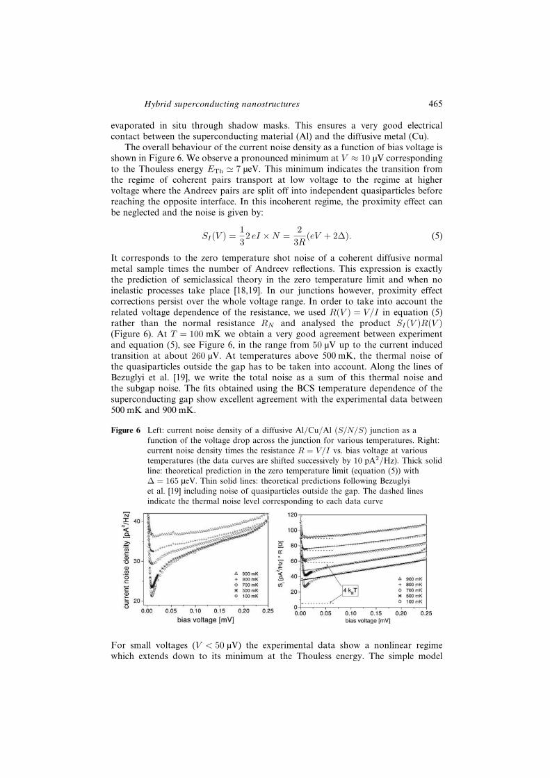
The overall behaviour of the current noise density as a function of bias voltage isshown in Figure 6. We observe a pronounced minimum at V ≈ 10 µV correspondingto the Thouless energy ETh ' 7 µeV. This minimum indicates the transition fromthe regime of coherent pairs transport at low voltage to the regime at highervoltage where the Andreev pairs are split off into independent quasiparticles beforereaching the opposite interface. In this incoherent regime, the proximity effect canbe neglected and the noise is given by:
SI(V ) =1
32 eI × N =
2
3R(eV + 2∆). (5)
It corresponds to the zero temperature shot noise of a coherent diffusive normalmetal sample times the number of Andreev reflections. This expression is exactlythe prediction of semiclassical theory in the zero temperature limit and when noinelastic processes take place [18,19]. In our junctions however, proximity effectcorrections persist over the whole voltage range. In order to take into account therelated voltage dependence of the resistance, we used R(V ) = V/I in equation (5)rather than the normal resistance RN and analysed the product SI(V )R(V )(Figure 6). At T = 100 mK we obtain a very good agreement between experimentand equation (5), see Figure 6, in the range from 50 µV up to the current inducedtransition at about 260 µV. At temperatures above 500 mK, the thermal noise ofthe quasiparticles outside the gap has to be taken into account. Along the lines ofBezuglyi et al. [19], we write the total noise as a sum of this thermal noise andthe subgap noise. The fits obtained using the BCS temperature dependence of thesuperconducting gap show excellent agreement with the experimental data between500 mK and 900 mK.
Figure 6 Left: current noise density of a diffusive Al/Cu/Al (S/N/S) junction as afunction of the voltage drop across the junction for various temperatures. Right:current noise density times the resistance R = V/I vs. bias voltage at varioustemperatures (the data curves are shifted successively by 10 pA2/Hz). Thick solidline: theoretical prediction in the zero temperature limit (equation (5)) with∆ = 165 µeV. Thin solid lines: theoretical predictions following Bezuglyiet al. [19] including noise of quasiparticles outside the gap. The dashed linesindicate the thermal noise level corresponding to each data curve
For small voltages (V < 50 µV) the experimental data show a nonlinear regimewhich extends down to its minimum at the Thouless energy. The simple model
466 C. Chapelier et al.
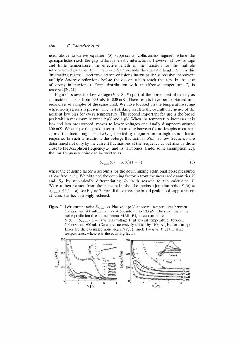
used above to derive equation (5) supposes a ‘collisionless regime’, where thequasiparticles reach the gap without inelastic interactions. However at low voltageand finite temperature, the effective length of the junction for the multipleretroreflected particles Leff = NL ∼ L∆/V exceeds the inelastic length Lin. In this‘interacting regime’, electron-electron collisions interrupt the successive incoherentmultiple Andreev reflections before the quasiparticles reach the gap. In the caseof strong interaction, a Fermi distribution with an effective temperature Te isrestored [20,21].
Figure 7 shows the low voltage (V < 8 µV) part of the noise spectral density asa function of bias from 500 mK to 800 mK. These results have been obtained in asecond set of samples of the same kind. We have focused on the temperature rangewhere no hysteresis is present. The first striking result is the overall divergence of thenoise at low bias for every temperature. The second important feature is the broadpeak with a maximum between 2 µV and 4 µV. When the temperature increases, it isless and less pronounced, moves to lower voltages and finally disappears around800 mK. We analyse this peak in terms of a mixing between the ac-Josephson currentIJ and the fluctuating current δIN generated by the junction through its non-linearresponse. In such a situation, the voltage fluctuations S(ω) at low frequency aredetermined not only by the current fluctuations at the frequency ω, but also by thoseclose to the Josephson frequency ωJ and its harmonics. Under some assumption [22],the low frequency noise can be written as
SImeas(0) = SI(0)(1 − η), (6)
where the coupling factor η accounts for the down mixing additional noise measuredat low frequency. We obtained the coupling factor η from the measured quantities Vand Rd by numerically differentiating Rd with respect to the calculated I .We can then extract, from the measured noise, the intrinsic junction noise SI(0) =SImeas
(0)/(1 − η), see Figure 7. For all the curves the broad peak has disappeared or,at least, has been strongly reduced.
Figure 7 Left: current noise SImeasvs. bias voltage V at several temperatures between
500 mK and 800 mK. Inset: SI at 500 mK up to 120 µV. The solid line is thenoise prediction due to incoherent MAR. Right: current noiseSI(0) = SImeas
/(1 − η) vs. bias voltage V at several temperatures between500 mK and 800 mK (Data are successively shifted by 100 pA2/Hz for clarity).Lines are the calculated noise 4kBT/(V/I). Inset: 1 − η vs. V at the sametemperatures, where η is the coupling factor
Hybrid superconducting nanostructures 467
Figure 7 shows that SI(0) exhibits a strong divergence at low voltage, whichcannot be described by the thermal noise of the normal resistance 4kBT/RN as inKoch et al. [23]. We cannot either understand the data by introducing an effectivetemperature, as we would get an unrealistic effective temperature as high as 100 K.We thus propose that the low voltage noise writes as
SI(0) =4kBT
V/I. (7)
The comparison with experimental data of SI(0) is shown in Figure 7 with noadjustable parameter. Between 800 mK and 550 mK, the agreement is remarkable.Equation (7) can be understood in two ways. First, it is the low voltage limit(eV & kBT ) of the quasiparticle noise of a junction with low transmitting channels:SI(0) = 2eI coth(eV/2kBT ). If effective charges e∗ > e are responsible for thetransport, e should be replaced by e∗ = Ne in the above expressions. In that case,the condition e∗V = NeV & kBT for equation (7) to remain valid, is verified aslong as N < 30 at 1 µV and 550 mK. In this description, only channels with lowtransmission coefficients contribute to the current and to the noise. Equation (7)might also be related to the fluctuation – dissipation theorem in a non-linear system,in which the resistance RN would be replaced by V/I(V ). Here, dissipation arisesfrom electron-electron interactions that necessarily occur at low voltage due to thelarge number of Andreev reflections needed for the quasiparticles to escape into thesuperconducting electrodes. In both cases, we conclude that, at very low voltage and‘high’ temperature, the current noise in long S/N/S junctions is governed by thetransport of incoherent quasiparticles between the two superconducting reservoirs,which induces a noise divergence when the voltage goes to zero [18].
When decreasing further the temperature, the experimental data present a largeexcess noise compared to equation (7) expression. Therefore, additional noisesources must be involved. It is worth noting that this deviation from a purequasiparticles noise occurs below 525 mK, which corresponds to kBT ' 3.5 ETh,very close to the mini-gap width (3.1 ETh) [22]. This suggests that coherentprocesses, which become relevant in this energy scale, should play a role here.
4 Micro-cooling in hybrid devices
In a N-I-S tunnel junction (where I stands for Insulator), single quasi-particles cantunnel from the normal metal to the superconductor if their energy, as measuredfrom the superconductor Fermi level, is larger than the superconducting gap. Thisenergy selectivity induces a cooling of the electronic population of the normal metalin a S-I-N junction biased at a voltage below the gap ∆/e. As the heat currentdirection does not depend on the sign of the bias, S-I-N-I-S micro-coolers based ona double tunnel junction feature a double cooling power and an improved efficiencydue to the better thermal isolation of the metal. The electronic temperature reductionreaches an optimum at a voltage bias just below the gap. In a Al-based device,normal metal electrons can cool from a bath temperature of 300 mK down to below100 mK [24,25].
We have studied the electron transport properties of S-I-N-I-S electronicmicro-coolers down to very low cryostat temperature (90 mK) [26]. A differential

468 C. Chapelier et al.
conductance peak is observed at zero bias and identified as the contributionof the Andreev reflection to the sub-gap current, see Figure 8 left. As thetemperature is decreased, this Andreev current increases, as it arises from the phasecoherence in the normal metal. We have shown that the Andreev current introducesadditional dissipation in the normal metal, equivalent to Joule heating. By analysingquantitatively the heat balance in the superconducting micro-cooler, we provide afull description of the evolution of the electronic temperature with the voltage. Thedissipation induced by the Andreev current is found to dominate the single particletunnelling-based cooling over a large bias range, see Figure 8 right. This newlyuncovered contribution is thus of great importance for the analysis of the thermalbehaviour of superconducting micro-coolers as well as of other hybrid devices.
Figure 8 Left: differential conductances measured at a cryostat temperature of 90 mK.Top (red) curve: data of one probe junction 1.55 µm from the cooler junctionand of normal-state resistance RN = 2.76 kΩ. The black dotted line is a fitdescribing the single quasi-particle tunnelling current. Bottom (blue) curve: coolerjunction data with a normal state resistance RN = 1.9 kΩ. Inset: schematics andmicrograph of a cooler made of two Al-AlO(x)-Cu junctions in series. The areaof a cooler junction is 1.5 × 0.3 µm2. In addition to the cooler, one of the threeAl-AlOx-Cu probe junctions on the bottom superconducting electrode is visible.The superconducting gap is 2∆ = 0.43 meV. The voltage axis is normalised to ∆
(probe data) or 2∆ (cooler data). Right: normalised differential conductance ofthe cooler junction as a function of voltage at different cryostat temperatures:240 (purple), 140 (green) and 90 mK (blue line) (see online version for colours)
5 Conclusion and perspectives
The studies of hybrid superconducting nanostructures described in this paperoffer new inroads into mesoscopic physics, nanoscale devices and low temperatureexperimental developments which provide the ground for ongoing researchs inGrenoble. Apart from unexpected observations in granular superconductors [27],proximity effect in diffusive systems is well understood, and many experiments

Hybrid superconducting nanostructures 469
have been performed to investigate it on a mesoscopic scale [16,28,29]. Proximityeffects in ballistic materials remains a difficult experimental challenge. However,a breakthrough can be done with the recent discovery of graphene [30]. Thisnew material made of a single atomic layer of carbon atoms arranged on ahexagonal array is expected to allow ballistic transport on very long distances upto several microns. Moreover, because of a peculiar band structure, under certaincircumstances, Andreev conversion of an electron into a hole and a Cooper pair isassociated with a specular reflection. One can imagine devices where, by varying theFermi level of graphene with the help of an electrostatic gate, the transfer of currentbetween graphene and a superconductor can be tuned from a specular Andreevreflection into a usual retroreflection.
We have seen that inhomogeneous superconducting states can either be inducedby a magnetic field or artificially tailored by lithography techniques. A thirdpossibility is to weaken the superconductivity of a thin film by increasing itsdisorder. When impurities are incorporated or the film thickness reduced, the slowdiffusion of the electrons impairs their ability to screen Coulomb repulsion, whichcompetes with the attractive Cooper pairing. Ultimately, at a critical disorderand T = 0, a quantum transition happens, which drives the two-dimensionalsuperconductor into an insulator. Although disorder can be made homogeneousdown to a microscopic level, it is characterised by strong spatial fluctuations,like any statistical quantity. Close to the quantum superconductor-insulatortransition but on the superconducting side, these spatial fluctuations induce aninhomogeneous superconducting state on a mesoscopic scale [31]. Many works aredevoted to understand what kind of insulator can grow on this inhomogeneoussuperconducting state. Is it a Bose insulator where Cooper pairs still exist locallyor is it a Coulomb glass with only electronic-like excitations? Local probes but alsomesoscopic devices will probably shed light in a near future on these fundamentalquestions.
Requiring a metallic surface, STM is not well adapted for mesoscopic ornanoscopic structures built on insulating substrates. On the other hand, AtomicForce Microscopy (AFM) can image any kind of surface, but gives no informationabout electronic properties. We have developed a new kind of near field microscopywhich combines force microscopy with tunnelling spectroscopy, working at verylow temperatures [32]. This instrument, see Figure 9, can be used for near fieldstudies of nanostructures with partly insulating surfaces. To achieve this, we usea piezo-electric tuning fork on which we make electrical contact with a gluedtunnelling tip. The quartz tuning fork provides its natural rigidity to this hybridprobe, providing excellent stability for the tip in spectroscopic mode. The verylow working temperatures achieved for this microscope (50 mK) guarantee verygood energy resolution. We have studied the local superconducting properties fora sub-micron epitaxial wire of niobium on sapphire. The AFM image enabled usto localise the 8 nm high wire on the insulating sapphire surface. Once the point ispositioned on the metal wire, the microscope is switched over to tunnelling modeto do local spectroscopy, measuring the variation of the density of electronic stateswith position. This new experimental approach opens new perspectives for themeasurement of non-equilibrium effects in superconducting nanostructures.
Scanning nanoSQUID Microscopy has been successfully employed to study themagnetic state in crystals of unconventional superconductors [33,34]. Very often the

470 C. Chapelier et al.
surface state of these materials is so delicate that STM techniques fail to accessthe electronic bulk state, but magnetic microscopy can detect vortex arrangements,and particular magnetic states, spontaneous currents etc . . . The nanoSQUID forcemicroscopy has a huge potential of improvements: shaping tips by Si deep-etchingin order to come closer to the surface and increase the magnetic flux-coupling, novelSQUID readout schemes . . . Several orders of magnitude can be won in spatial,magnetic and temporal resolution. This progress will allow to observe dynamicprocesses, and magnetic noise in superconducting quantum devices to name just afew new potentialities.
Figure 9 Top, left: 115 × 950 nm2 AFM image of a 300 nm-wide Nb wire patterned on asapphire substrate at 100 mK. Frequency shift is 0.15 Hz, tip oscillationamplitude is 1 nm, scanning speed is 175 nm/s. Bottom: Differential conductancespectra acquired at 100 mK in units of the high bias conductance equals to50 MΩ. The spectroscopies from bottom to top were acquired along a25 nm-long displacement of the tip on the Nb wire as indicated by an arrow onthe image. Right: Photograph of a very low temperature AFM-STM operating at50 mK in a home-made upside-down dilution refrigerator. The motor stacksholding the sample are visible at the bottom and in front of the piezo-electrictube holding the tip (see online version for colours)
We have shown that current noise measurements provide a precise description ofelectronic transport in Josephson junctions. Having now a clear description of thecurrent noise in diffusive S/N/S junctions and in diffusive S/N contacts [35,36],we are now addressing the problem of crossed correlations in multi-terminalsuperconducting hybrid nanostructures. The idea is to fabricate a normalnanostucture that is connected to one or several superconducting electrodes. If thenanostructure is small enough, an Andreev pair emitted by one superconductingelectrode into the normal metal can split and one of the two quasiparticles
Hybrid superconducting nanostructures 471
can propagate in one electrode connected to the nanostructure and the secondquasiparticle in a different electrode. This crossed Andreev reflection process couldbe detected by crossed current correlations measurements. This would be the firststep towards the fabrication and the detection of an electronic Einstein-Podolsky-Rosen (EPR) source [37] (and references therein).
Acknowledgements
The authors would like to acknowledge their collaborators P. Achatz, E. Bustarret,O. Coupiac, L. Crétinon, F. Dahlem, V. Dolocan, T. Dubouchet, W. Escoffier,P. Gandit, A.K. Gupta, N. Hadacek, F.W.J. Hekking, C. Hoffmann, D. Hykel,T. Klein, E. Lhotel, P.S. Luo, C. Marcenat, N. Moussy, F. Omnes, Z. Osvath,B. Pannetier, L. Pascal, T. Quaglio, S. Rajauria, B. Sacépé, M. Sanquer, J. Senzier,J-C. Villégier, A. Vasenko, C. Veauvy-Ladam, M. Vinet.
References
1 Fink, H.J. (1965) ‘Internal currents and magnetic fields close to the surface for a type-IIsuperconductor for applied magnetic fields near the upper critical field Hc2’, Phys. Rev.Lett., Vol. 14, p.853.
2 Courtois, H., Gandit, P., Pannetier, B. and Mailly, D. (1999) ‘Long-range coherenceand mesoscopic transport in N-S metallic structures’, Superlattices Microstruct., Vol. 25,Nos. 5–6, pp.721–732.
3 Dubos, P., Courtois, H., Pannetier, B., Wilhelm, F., Zaikin, A. and Schön, G. (2001)‘The Josephson critical current in a long mesoscopic S-N-S junction’, Phys. Rev. B,Vol. 63, No. 6, p.064502.
4 Hasselbach, K., Veauvy, C. and Mailly, D. (2000) ‘Microsquid magnetometry andmagnetic imaging’, Physica C, Vol. 332, p.140.
5 Kirtley, J.R., Ketchen, M.B., Stawiasz, K.G., Sun, J.Z., Gallagher, W.J., Blanton, S.H.and Wind, S.J. (1995) ‘High-resolution scanning SQUID microscope’, Appl. Phys. Lett.,Vol. 66, p.1138.
6 Veauvy, C., Hasselbach, K. and Mailly, D. (2002) ‘Scanning µ-superconducting quantuminterference device force microscope’, Rev. Sci. Instrum., Vol. 73, p.3825.
7 Veauvy, C., Hasselbach, K. and Mailly, D. (2004) ‘Micro-squid microscopy of vorticesin a perforated superconducting Al film’, Phys. Rev. B, Vol. 70, p.214513, 5 pages.
8 Buzdin, A.I. (1993) ‘Multiple-quanta vortices at columnar defects’, Phys. Rev. B, Vol. 47,p.11416.
9 Moussy, N., Courtois, H. and Pannetier, B. (2001a) ‘A very low temperature scanningtunnelling microscope for the local spectroscopy of mesoscopic structures’, Rev. Sci.Instrum., Vol. 72, No. 1, pp.128–131.
10 Hess, H.F., Robinson, R.B., Dynes, R.C., Valles, J.M. and Waszczak, J.V. (1989)‘Scanning-tunneling-microscope observation of the Abrikosov flux lattice and the densityof states near and inside a fluxoid’, Phys. Rev. Lett., Vol. 62, No. 2, p.214.
11 Hess, H.F., Robinson, R.B. and Waszczak, J.V. (1990) ‘Vortex-core structure observedwith a scanning tunnelling microscope’, Phys. Rev. Lett., Vol. 64, No. 22, p.2711.
12 Renner, Ch., Kent, A.D., Niedermann, Ph., Fischer, Ø. and Lévy, F. (1991) ‘Scanningtunnelling spectroscopy of a vortex core from the clean to the dirty limit’, Phys. Rev.Lett., Vol. 67, No. 12, p.1650.
472 C. Chapelier et al.
13 Sacépé, B., Chapelier, C., Marcenat, C., Kacmarcik, J., Klein, T., Bernard, M. andBustarret, E. (2006a) ‘Tunneling spectroscopy and vortex imaging in boron-dopeddiamond’, Phys. Rev. Lett., Vol. 96, No. 9, p.097006.
14 Sacépé, B., Chapelier, C., Marcenat, C., Kacmarcik, J., Klein, T., Omnes, F. andBustarret, E. (2006b) ‘Experimental indications of a BCS behaviour in superconductingdiamond’, Phys. Status Solidi A, Vol. 203, No. 13, p.3315.
15 Bustarret, E., Achatz, P., Sacépé, B., Chapelier, C., Marcenat, C., Ortega, L. andKlein, T. (2008) ‘Metal-to-insulator transition and superconductivity in boron-dopeddiamond’, Philos. Trans. R. Soc. A, Vol. 366, p.267.
16 Moussy, N., Courtois, H. and Pannetier, B. (2001b) ‘Local spectroscopy of a proximitysuperconductor at very low temperature’, Europhys. Lett., Vol. 55, No. 6, pp.861–867.
17 Gupta, A.K., Crétinon, L., Moussy, N., Courtois, H. and Pannetier, B. (2004)‘Anomalous density of states in a metallic film in proximity with a superconductor’,Phys. Rev. B, Vol. 69, No. 10, p.104514.
18 Nagaev, K.E. (2001) ‘Frequency-dependent shot noise in long disordered-normal-metal-superconductor contacts’, Phys. Rev. Lett., Vol. 86, No. 14, p.3112.
19 Bezuglyi, E.V., Bratus, E.N.v., Shumeiko, V.S. and Wendin, G. (2001) ‘Current noisein long diffusive SNS junctions in the incoherent multiple Andreev reflections regime’,Phys. Rev. B, Vol. 63, No. 10, p.100501.
20 Hoss, T., Strunk, C., Nussbaumer, T., Huber, R., Staufer, U. and Schonenberger, C.(2000) ‘Multiple Andreev reflection and giant excess noise in diffusivesuperconductor/normal-metal/superconductor junctions’, Phys. Rev. B, Vol. 62, No. 6,p.4079.
21 Hoffmann, C., Lefloch, F. and Sanquer, M. (2002) ‘Inelastic relaxation and noisetemperature in S/N/S junctions’, Eur. Phys. J. B, Vol. 29, No. 4, p.629.
22 Lhotel, E., Coupiac, O., Lefloch, F., Courtois, H. and Sanquer, M. (2007) ‘Divergenceat low bias and down-mixing of the current noise in a diffusive superconductor-normal-metal-superconductor junction’, Phys. Rev. Lett., Vol. 99, No. 11, p.117002.
23 Koch, R.H., Van Harlingen, D.J. and Clarke, J. (1982) ‘Measurements of quantum noisein resistively shunted Josephson junctions’, Phys. Rev. B, Vol. 26, No. 1, p.74.
24 Giazotto, F., Heikkila, T.T., Luukanen, A., Savin, A.M. and Pekola, J.P. (2006)‘Opportunities for mesoscopics in thermometry and refrigeration: physics andapplications’, Rev. Mod. Phys., Vol. 78, No. 1, p.217.
25 Rajauria, S., Luo, P.S., Fournier, T., Hekking, F.W.J., Courtois, H. and Pannetier, B.(2007) ‘Electron and phonon cooling in a superconductor-normal-metal-superconductortunnel junction’, Phys. Rev. Lett., Vol. 99, No. 4, p.047004.
26 Rajauria, S., Gandit, P., Fournier, T., Hekking, F.W.J., Pannetier, B. and Courtois, H.(2008) ‘Andreev current-induced dissipation in a hybrid superconducting tunneljunction’, Phys. Rev. Lett., Vol. 100, No. 20, p.207002.
27 Escoffier, W., Chapelier, C., Hadacek, N. and Villégier, M. (2004) ‘Anomalous proximityeffect in an inhomogeneous disordered superconductor’, Phys. Rev. Lett., Vol. 93,No. 21, p.217005.
28 Vinet, M., Chapelier, C. and Lefloch, F. (2001) ‘Spatially resolved spectroscopy onsuperconducting proximity nanostructures’, Phys. Rev. B, Vol. 63, No. 16, p.165420.
29 Escoffier, W., Chapelier, C. and Lefloch, F. (2005) ‘Ballistic effects in a proximityinduced superconducting diffusive metal’, Phys. Rev. B, Vol. 72, No. 72, p.140502(R).
30 Novoselov, K.S., Geim, A.K., Morozov, S.V., Jiang, D., Zhang, Y., Dubonos, S.V.,Grigorieva, I.V. and Firsov, A.A. (2004) ‘Electric field effect in atomically thin carbonfilms’, Science, Vol. 306, p.666.

Hybrid superconducting nanostructures 473
31 Sacépé, B., Chapelier, C., Baturina, T.I., Vinokur, V.M., Baklanov, M.R. andSanquer, M. (2006) ‘Disorder-induced inhomogeneities of the superconducting stateclose to the superconductor-insulator transition’, Phys. Rev. Lett., Vol. 101, No. 15,p.157006.
32 Senzier, J., Luo, P.S. and Courtois, H. (2007) ‘Combined scanning force microscopy andscanning tunnelling spectroscopy of an electronic nanocircuit at very low temperature’,Appl. Phys. Lett., Vol. 90, No. 4, p.043114.
33 Dolocan, V.O., Veauvy, C., Servant, F., Lejay, P., Liu, Y., Mailly, D. and Hasselbach, K.(2005) ‘Observation of vortex coalescence in the anisotropic spin-triplet superconductorSr2RuO4’, Phys. Rev. Lett., Vol. 95, p.97004.
34 Dolocan, V.O., Lejay, P., Mailly, D. and Hasselbach, K. (2006) ‘Observation of twospecies of vortices in the anisotropic spin-triplet superconductor Sr2RuO4’, Phys. Rev. B,Vol. 74, p.144505.
35 Jehl, X., Sanquer, M., Calemczuk, R. and Mailly, D. (2000) ‘Detection of doubled shotnoise in short normal-metal/superconductor junctions’, Nature, Vol. 405, p.50.
36 Lefloch, F., Hoffmann, C., Sanquer, M. and Quirion, D. (2000) ‘Doubled full shotnoise in quantum coherent superconductor-semiconductor junctions’, Phys. Rev. Lett.,Vol. 90, p.067002.
37 Duhot, S., Houzet, M. and Lefloch, F. (2009) ‘Cross correlation of incoherent multipleAndreev reflections’, Phys. Rev. Lett., Vol. 102, p.086804.