hybrid pcb stack-up - intel · 330559-001 3 figure 1. hybrid pcb stack-up illustration microstrip...
TRANSCRIPT

Intel Corporation
Data Center Platform Application Engineering
April 2014
Reference Number: 330559-001
Hybrid PCB Stack-up
Optimization of PCB Cost and Loss Performance
2 330559-001
Introduction
Signal attenuation over a transmission line (TL) on a printed circuit board (PCB) becomes more significant when the transfer rate of a SerDes link increases such like PCIe* Gen 3 at
8 Gbps to PCIe Gen 4 at 16 Gbps. Typical insertion loss (IL) for PCBs built with FR4 is about -0.2 dB/inch/GHz for differential signaling. There are different approaches to
improve signal integrity (SI) performance when dealing with the challenge of IL, such as
transmitter and receiver equalizations, re-driver and re-timer, and low loss PCB materials. Normally, a low loss PCB stack-up costs more than an FR4 stack-up. However, from SI
design perspective, not every IO needs low loss. Therefore, if a PCB stack-up is designed with some layers as low loss but other layers as high loss (FR4), then it can meet the
same or similar low loss performance requirement for the IOs but at a lower cost that an all low loss board. This is the key advantage of a hybrid PCB stack-up.
Hybrid PCB Stack-up
The hybrid PCB stack-up can be used as one of enablers to improve SI for signals routed on selected layers. For a hybrid PCB stack-up, some layers of the PCB use low loss dielectric while the others are fabricated with the traditional FR4. The cost of such a hybrid
stack-up is normally lower than all low loss material PCB stack-up, but with the advantage of some routing layers having the same or similar low loss properties as an all low loss
stack-up, thus achieving optimized cost-performance. As a contrast to re-driver/re-timer
solution which improves SI performance for selected number of links, a hybrid PCB stack-up can improve SI performance for selected routing layers. A hybrid stack-up can also be
built by mixing low loss material with ultra-low loss material to further reduce loss in the routing. In short, a hybrid PCB stack-up has the following features:
Performance improvement over the stack-ups with all standard FR4 board
Cost reduction over stack-ups with all low-loss/medium-loss board.
There are different options and associated costs for creating a hybrid PCB stack-up. For
example, one can use same materials (high loss or low loss) for all the prepreg(PP) layers, and different types of materials for core layers. Another example is to form top and
bottom layers as low loss while keeping all other layers FR4, thus having two microstrip routing layers as low loss. Figure 1 shows some implementation options.

330559-001 3
Figure 1. Hybrid PCB stack-up illustration
Microstrip in Hybrid PCB Stack-up
For microstrip, a hybrid PCB stack-up has the same performance as all low loss stack-ups, as long as the dielectric of the outer layer is low loss. In other words, if the signals
requiring low loss material are only routed on outer layers, the hybrid PCB can get the
identical loss performance compared to all-low-loss stack-up, while significantly reduces the material cost.
Stripline in Hybrid PCB Stack-up
For stripline as shown in Figure 2, the signal may not get full benefit of low loss material
unless both sides of the dielectric is low loss material. As shown in Figure 2, very often, for stripline in a hybrid PCB stack-up, one side of material is low loss while the other side
of material is high loss.
For stripline with high loss and low loss dielectric materials on the top and the bottom of the signal layer as shown in Figure 2, the loss is expected to be higher than striplines with
same stack-up of all low loss materials on both sides, but lower than striplines with same
stack-up using high loss materials on both sides.
Figure 2. Stripline in a hybrid PCB stack-up
Low Loss
Low Loss
Preferred
4 330559-001
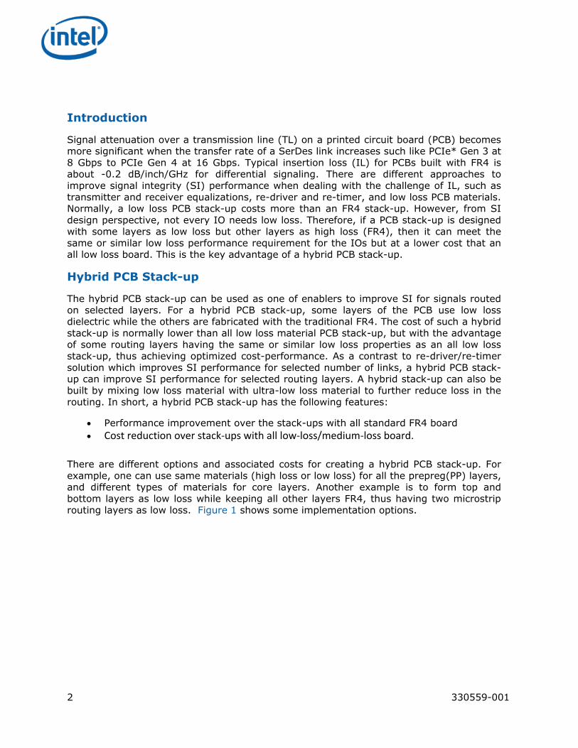
(a). Test board of hybrid PCB Stackup
(b). 27” stripline loss with different materials
Figure 3. Hybrid PCB result
For asymmetric striplines as shown in Figure 2, in order to achieve the optimal performance, it is preferred to have thinner layer using low loss, as most of the energy of
the transmitting signals will be in the thinner layer.
In order to demonstrate loss improvement for hybrid PCB stack-up, test boards were fabricated and VNA S-parameter measurement has been performed. The stack-up is shown in Figure 3(a), in which E3 and E6 are the hybrid stripline routing layers. For
comparison purpose, two other boards with same stack-up were also built: boards using FR4 and board using low materials corresponding to Figure 3(a). Figure 3(b) is the
measured S-parameter of 27” stripline from three boards: all layers FR4, all layers low
loss and a hybrid stack-up. Loss improvement can be obviously seen from Figure 3(b).
330559-001 5
The overall loss of transmission lines with high/low loss dielectric materials depends on
material selection, stack-up, and so forth. Simulation can be used to estimate the PCB trace loss. Test boards or test coupons can be built to validate the PCB trace loss.
Other electrical properties such PCB impedance, crosstalk, and power delivery performance can be covered in simulation as well.
Feasibility, Test and Manufacturing
Manufacturing capability and the stack-up implementation recipe for a hybrid PCB can differ among PCB manufacturers. The optimal performance-cost solution also depends on
the number of signal layers, routing length, material selection, etc. It is necessary to
consult your PCB manufacture for the capability and the risk associated such as the yield, de-lamination, etc.
Intel Data Center Platform Application Engineer (DCPAE) team is currently working with PCB vendors for a Hybrid PCB Stack-up Vendor Status Update - a list of vendors which can provide hybrid PCB stack-up.
A hybrid PCB stack-up should go through same test procedures as normal PCB stack-up. These tests are related to different areas of thermal, mechanical, reliability, de-laminating,
yielding, and environmental, and so forth.
Below is an example list of tests that could be done. It is PCB vendors’ role and
responsibility to define and complete a series of tests similar to the list below before it goes to high volume manufacturing (HVM):
Example Reliability Testing: o Time to Delamination (T260/T288) o Interconnect Stress Test (IST) for through-hole integrity
o Thermal Stress (aka solder float)
o Temperature Cycle o Etc.
PCB Supplier UL Approval o Hybrid designs are often custom and may not be UL approved depending on
construction o Suppliers may need to get UL approval which takes months and can be a
significant cost adder
Cost Reduction Opportunity
Cost quotes for a hybrid PCB stack-up can vary due to materials used, stack-up configuration, volume, vendor choice and turn time. Please consult PCB vendors for the capability and quotation.
Figure 4 shows quotation examples from one PCB vendor. It represents quotation trends only. The quotations for 8L, 10L, 12L and 14L stack-ups represent different core or
prepreg low loss combinations. The low loss material used for this quotation is with

6 330559-001
relative permittivity Er=4.1, loss tangent=0.012 at 5 GHz, which is actually a medium loss
material. The quotation for 8L FR4 PCB stack-up is noted as “1” for benchmarking purpose.
Based on feedback from the PCB vendors visited, normally, a hybrid PCB stack-up should cost less than the all low loss material stack-up.
Figure 4. Quotation for different hybrid PCB stack-up options
Routing and Power Delivery
Routing such as trace width and spacing is relevant to the stack-up and materials to be used to form the stack-up. For hybrid PCB stack-up, routing is similar as FR4 or low loss stack-up. For stripline, if permittivity Er of up (Er1) and bottom (Er2) dielectric materials
are very different, bigger pair to pair spacing than that for same or similar Er value of
materials can be considered to mitigate crosstalk impact. Please refer to Appendix A(c) for more discussions.
For hybrid PCB stack-up, if the stack-up is same but only changing dielectric material from high loss to low loss stack-up, there is very minor difference from high loss or low loss stack-up, because for power delivery, the interested frequency range is below 1 GH.
Summary
A hybrid PCB stack-up provides an enabler to improve signal integrity performance for high-speed signaling at a potential lower cost than an all low loss stack-up. Test boards
were built to have verified the SI performance improvement. More detail data is given in Appendix A. System designers should consult their PCB vendors for cost, loss
performance, and manufacturing.
0
0.5
1
1.5
2
2.5
All FR4 All PP ML 2 Cores ML All PP + 2Core ML
4 Cores ML All PP + 4cores ML
All ML
8 Layer
10 Layer
12 Layer
14 Layer

330559-001 7
Appendix A: Signal Integrity Study
a) Transmission lines and loss in hybrid PCB stack-up
In a hybrid PCB stack-up, there are different types of microstrip and stripline. Figure A1 shows nine different cases. Cases 1 to 3 are symmetrical stripline; cases 4~7 are
asymmetrical stripline. Cases 8 and 9 are microstrip for low loss or FR4. Material properties and layer thicknesses are two of key factors determining IL and crosstalk of TL.
Two dimensional field solvers can be used to calculate loss and crosstalk. For microstrip, the structure is same whether it is hybrid or non-hybrid, so we will focus on stripline,
which can be different between hybrid and non-hybrid stack-ups.
Figure A2 and Figure A3 is the calculated loss for 10” striplines. All the striplines are 85Ω differential with trace width of 5 mils. FR4 material has a relative permittivity Er equal to
4.1 and a loss tangent equal to 0.022. For low loss material, Er is 3.71 and loss tangent is
0.0127. The metal has conductivity equal to 5.8E7 S/m. Surface roughness is taken into account with the Huray model.
(1) (2) (3)
(4) (5) (6)
(7) (8) (9)
Dielectric 1
Dielectric 2
Figure A1. Transmission lines in a hybrid PCB stack-up

8 330559-001
Figure A2. Insertion loss for Cases 1, 2, 3 of Figure A1.
330559-001 9
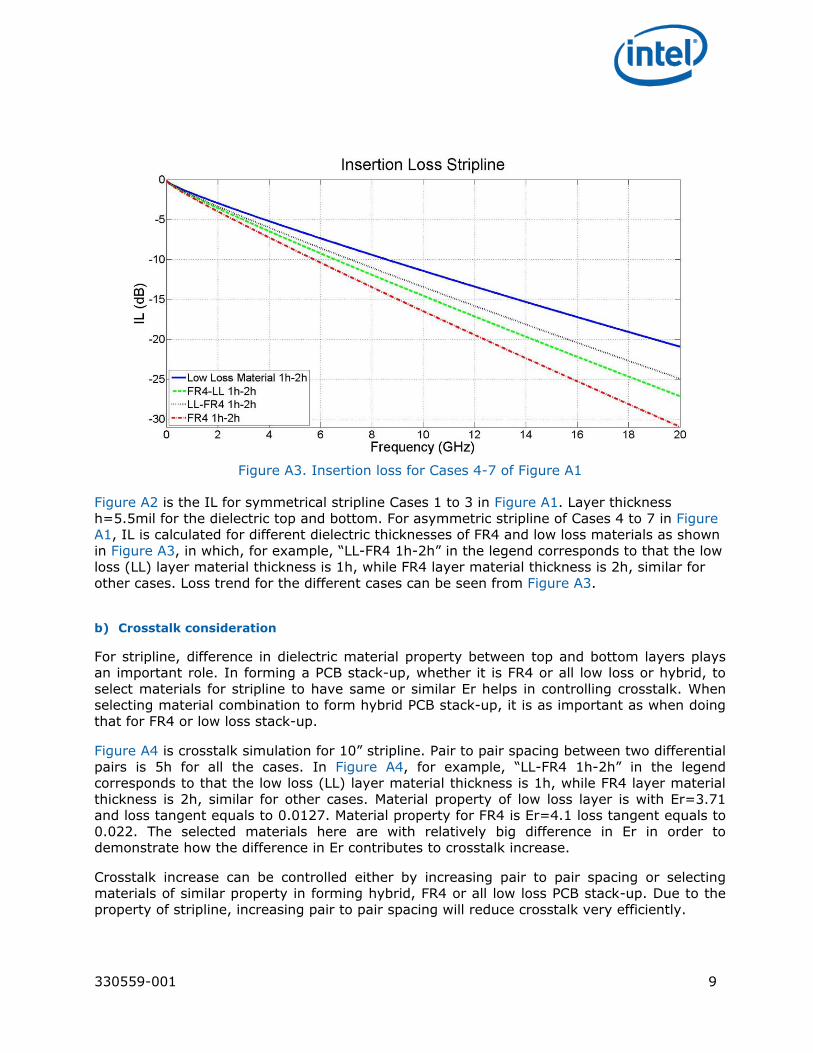
Figure A3. Insertion loss for Cases 4-7 of Figure A1
Figure A2 is the IL for symmetrical stripline Cases 1 to 3 in Figure A1. Layer thickness
h=5.5mil for the dielectric top and bottom. For asymmetric stripline of Cases 4 to 7 in Figure A1, IL is calculated for different dielectric thicknesses of FR4 and low loss materials as shown
in Figure A3, in which, for example, “LL-FR4 1h-2h” in the legend corresponds to that the low loss (LL) layer material thickness is 1h, while FR4 layer material thickness is 2h, similar for
other cases. Loss trend for the different cases can be seen from Figure A3.
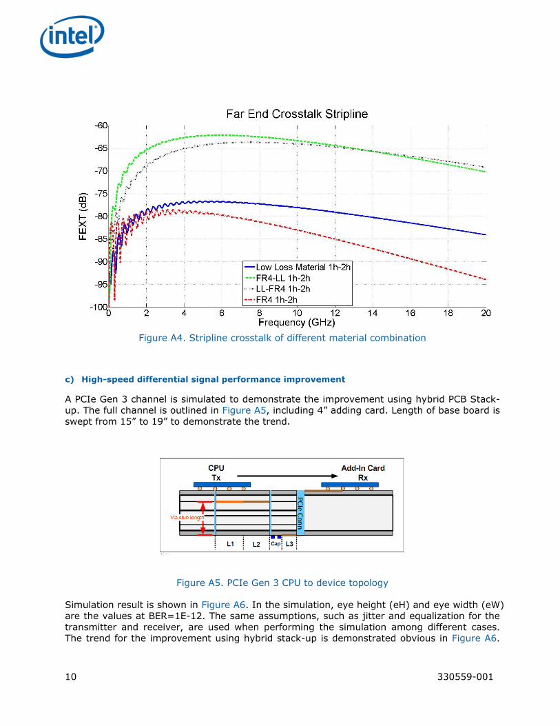
b) Crosstalk consideration
For stripline, difference in dielectric material property between top and bottom layers plays an important role. In forming a PCB stack-up, whether it is FR4 or all low loss or hybrid, to
select materials for stripline to have same or similar Er helps in controlling crosstalk. When selecting material combination to form hybrid PCB stack-up, it is as important as when doing
that for FR4 or low loss stack-up.
Figure A4 is crosstalk simulation for 10” stripline. Pair to pair spacing between two differential
pairs is 5h for all the cases. In Figure A4, for example, “LL-FR4 1h-2h” in the legend corresponds to that the low loss (LL) layer material thickness is 1h, while FR4 layer material
thickness is 2h, similar for other cases. Material property of low loss layer is with Er=3.71 and loss tangent equals to 0.0127. Material property for FR4 is Er=4.1 loss tangent equals to
0.022. The selected materials here are with relatively big difference in Er in order to demonstrate how the difference in Er contributes to crosstalk increase.
Crosstalk increase can be controlled either by increasing pair to pair spacing or selecting materials of similar property in forming hybrid, FR4 or all low loss PCB stack-up. Due to the
property of stripline, increasing pair to pair spacing will reduce crosstalk very efficiently.
10 330559-001
Figure A4. Stripline crosstalk of different material combination
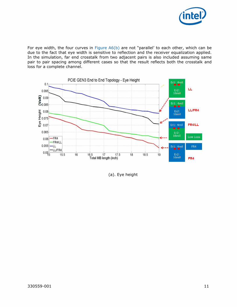
c) High-speed differential signal performance improvement
A PCIe Gen 3 channel is simulated to demonstrate the improvement using hybrid PCB Stack-up. The full channel is outlined in Figure A5, including 4” adding card. Length of base board is
swept from 15” to 19” to demonstrate the trend.
Figure A5. PCIe Gen 3 CPU to device topology
Simulation result is shown in Figure A6. In the simulation, eye height (eH) and eye width (eW) are the values at BER=1E-12. The same assumptions, such as jitter and equalization for the
transmitter and receiver, are used when performing the simulation among different cases. The trend for the improvement using hybrid stack-up is demonstrated obvious in Figure A6.
330559-001 11
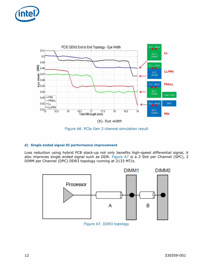
For eye width, the four curves in Figure A6(b) are not “parallel’ to each other, which can be
due to the fact that eye width is sensitive to reflection and the receiver equalization applied. In the simulation, far end crosstalk from two adjacent pairs is also included assuming same
pair to pair spacing among different cases so that the result reflects both the crosstalk and loss for a complete channel.
(a). Eye height
12 330559-001
(b). Eye width
Figure A6. PCIe Gen 3 channel simulation result
d) Single ended signal SI performance improvement
Loss reduction using hybrid PCB stack-up not only benefits high-speed differential signal, it also improves single ended signal such as DDR. Figure A7 is a 2 Slot per Channel (SPC), 2 DIMM per Channel (DPC) DDR3 topology running at 2133 MT/s.
Figure A7. DDR3 topology

330559-001 13
Eye height (EH) and eye width (EW) for different stripline options including FR4, low loss and two combinations of hybrid stripline are given in Figure A8.
The EH and EW margin values are the statistic mean values obtained from Monte Carlo analysis performed considering package and board impedance corners, silicon PVT (process, voltage, temperature) corners, different channel lengths, etc. In the simulation, the same assumptions are used to simulate the 4 different scenarios; the only difference is the stripline model used in the simulation. Improvement using hybrid is observed in the Figure A8. Hybrid of FR4 (LL/FR4) and all Low Loss (LL) show similar margins (<1 mV, <1 ps variation).
Using hybrid solution (LL/FR4) over a full FR4 stack-up can improve the performance on average by 7 mV and 10ps; for this specific configuration the average improvement of 7 mV/10 ps using the LL/FR4 stack-up corresponds to a risk level reduction from high to medium/low.
Figure A8. SI improvement for DDR3
Reference [1] Cesar Mendez Ruiz, Chunfei Ye; Xiaoning Ye; Enrique Lopez, Maoxin Yin ; Jimmy Hsu,
Thonas Su: Improve Signal Integrity Performance by Using Hybrid PCB Stackup, IEEE EMC Symposium, August 2013, pp317-321
[2] Thonas Su, Jimmy Hsu, Chunfei Ye ; Xiaoning Ye, Adrian Grigoras: Signaling Enabler in High-speed System Design by Using Hybrid Stack-up Printed Circuit Board, IMPACT, October 2013, pp85-88