hybrid nano-scale au with ito structure for a high
TRANSCRIPT

Hybrid nano-scale Au with ITO structure for ahigh-performance near-infrared silicon-basedphotodetector with ultralow dark currentXINXIN LI,1,2,3 ZHEN DENG,1,3,4,* JUN LI,1,3 YANGFENG LI,1,3 LINBAO GUO,1,2,3 YANG JIANG,1,3 ZIGUANG MA,1,3
LU WANG,1,3 CHUNHUA DU,1,3,4 YING WANG,5 QINGBO MENG,1,3 HAIQIANG JIA,1,3,6 WENXIN WANG,1,3,6
WUMING LIU,1 AND HONG CHEN1,3,6,7
1Key Laboratory for Renewable Energy, Beijing Key Laboratory for New Energy Materials and Devices, Beijing National Laboratory for CondensedMatter Physics, Institute of Physics, Chinese Academy of Sciences, Beijing 100190, China2University of Chinese Academy of Sciences, Beijing 100049, China3Center of Materials and Optoelectronics Engineering, University of Chinese Academy of Sciences, Beijing 100049, China4The Yangtze River Delta Physics Research Center, Liyang 213000, China5Department of Physics, School of Science, Beijing Jiaotong University, Beijing 100044, China6Songshan Lake Materials Laboratory, Dongguan 523808, China7e-mail: [email protected]*Corresponding author: [email protected]
Received 25 May 2020; revised 4 August 2020; accepted 19 August 2020; posted 20 August 2020 (Doc. ID 398450); published 9 October 2020
An internal photoemission-based silicon photodetector detects light below the silicon bandgap at room temper-ature and can exhibit spectrally broad behavior, making it potentially suited to meet the need for a near-infraredpure Si photodetector. In this work, the implementation of a thin Au insertion layer into an ITO/n-Si Schottkyphotodetector can profoundly affect the barrier height and significantly improve the device performance. Byfabricating a nanoscale thin Au layer and an ITO electrode on a silicon substrate, we achieve a well-behavedITO/Au/n-Si Schottky diode with a record dark current density of 3.7 × 10⁻⁷ A∕cm2 at −1 V and a high recti-fication ratio of 1.5 × 10⁸ at �1 V. Furthermore, the responsivity has been obviously improved without sacri-ficing the dark current performance of the device by decreasing the Au thickness. Such a silicon-basedphotodetector with an enhanced performance could be a promising strategy for the realization of a monolithicintegrated pure silicon photodetector in optical communication. © 2020 Chinese Laser Press
https://doi.org/10.1364/PRJ.398450
1. INTRODUCTION
Optical communication has become one of the most importanttechnologies in modern society due to its excellent performanceof speed transmission and information capacity, and is widelyoperated at wavelengths of 850, 1310, and 1550 nm [1]. Sincethere is little light absorption in silicon for wavelengths longerthan 1100 nm, almost all researches have been aimed at850 nm photodetectors (PDs) in the complementary metal-ox-ide semiconductor (CMOS) technologies. For 1310 nm and1550 nm optical receivers, the PDs with excellent performanceare mostly based on compound semiconductors (III–V) andGe–Si materials [2–4], both of which have a higher materialscost. In addition, the compound semiconductors suffer fromnot being compatible with the standard Si-based CMOS plat-form [5–7]. Therefore, the development of Si PDs based onmature CMOS technology without additional material or pro-cess steps is an essential step for monolithic integrated opticalreceivers. To overcome such intrinsic drawbacks and extend the
response wavelength of Si-based PDs to telecom wavelengths,many new attempts have been proposed, including employingSi-based quantum dots (QDs) based on quantum confinementeffect (QCE) [8], combining Ge (0.67 eV) with Si [9,10], two-photon absorption (TPA) [11–13], plasmonic hot carriers [14],and defect mediated band-to-band photogeneration via mid-bandgap localized states [15–17]. However, some of these ap-proaches require complicated designs that limit their overallapplication. Recently, the Schottky diode has attracted muchattention due to its unique internal photoemission mechanism[18–22]. In this configuration, photoexcited carriers from themetal are emitted to the semiconductor over a potential ΦB ,called a Schottky barrier (SB), to generate the photocurrent[23]. Typically, an SB is lower than the intrinsic bandgap Egof a semiconductor, thus allowing the photodetection of pho-tons with energy hν < Eg, which is the basis for silicon-basedSchottky PDs (SPDs) to realize the detection above 1.1 μm[20,24,25]. For example, PtSi/p-Si SPDs are widely used for
1662 Vol. 8, No. 11 / November 2020 / Photonics Research Research Article
2327-9125/20/111662-09 Journal © 2020 Chinese Laser Press

infrared imaging in the 3–5 μm wavelength range with avery low SB height (SBH) (0.2 eV) [26,27], while for shorterwavelength application, Ti, Co, and Ni can be adopted becausetheir contacts on n-Si have the SBH of 0.5–0.7 eV [28].However, it is difficult for traditional metal-Si SPDs to achieveconsiderable performance in responsivity. Fortunately, trans-parent conductive glass (ITO) with good conductivity and lighttransmission is a promising alternative to metal for allowingsufficient light to enter the junction [29,30]. One of the chal-lenges for the ITO/Si detector is that the low SBH leads to highdark current, which will severely drag down the sensitivity ofthe detector. To increase the height of the ITO/Si barrier,inserting other materials including an insulator and metal be-tween the ITO and silicon has been performed [18,25,31].Among these materials, the insulator materials have a highseries resistance, while an Ag layer at least 8 nm thick is neededto form a high barrier with Si due to the poor film formingability of Ag, resulting in poor light transmittance of the elec-trode and thus a reduced response. In recent studies, the Au/SiSPDs with different kinds of plasmonic designs have had betterresponsivity, but the dark current for these structures is stillhigh [32–34].
In this work, we demonstrated the ITO/Au/n-Si PDs withthe best record of dark current density on the order of1 × 10−7 A∕cm2 (−0.1 V to −2 V) at present. The mechanismfor such low dark current density is a high SBH, resulting froma high work function of the Au insertion layer into the ITO/Si.Furthermore, for the new structure, the transparency of theelectrode has been obviously improved and higher photocur-rent is obtained by thinning the Au film. As a silicon-basedSPD with a record low dark current density, one can envisionits role for operation from visible light to a 1550 nm wave-length without damaging the light responsivity.
2. METHODS
A. Preparation of the ITO/Au/n-Si PDsFigure 1 illustrates the process flow of making ITO/Au/n-SiSPDs. The PDs were fabricated with a commercial epi-readyn-type (0.1–1 Ω·cm, 400� 10 μm) silicon substrate. First,the PD areas were defined by ultraviolet lithography using anegative resist (AR-U 4030) in leaf patterns with an area of0.0007 cm2. Before being sent to the electron beam evapora-tion (Ohmiker-50B) chamber for Au deposition at room tem-perature, the patterned substrates were dipped in a dilute HFsolution (H2O:HF � 10:1 for 1 min) for oxide removing.During the evaporation process, the deposition pressure wasmaintained below 2 × 10⁻⁶ Pa and the deposition rate was0.17 Å/s (1 Å = 0.1 nm) controlled by the current with a volt-age at 8 kV. In addition, the plate where the substrates wereplaced rotated at a rate of 8 r/min to ensure the uniformityof the film. After that, 100 nm ITO was immediately depositedon the Au film by a double chamber magnetron sputtering sys-tem (Shenyang Defeng Technology) at room temperatureunder Ar∕O2 atmosphere. During the sputtering process,the thickness was controlled by the sputtering time with a dep-osition rate of 0.93 Å/s. Finally, the ohmic contact on the back-side was realized by a 300 nm Al film using Ohmiker-50B witha deposition rate of 1.7 Å/s at room temperature after removing
the oxide by a dilute HF solution (H2O:HF � 10:1 for 1 min).To protect the ITO/Au electrode from the HF solution, thepositive resist (AZ 6130) was used as the protective layer duringthe removing process. The source of Au and Al in the Ohmiker-50B was the molten metal that came from the particles (purity,99%; particles diameter, 0.5 cm) by heating an electron beamin the crucible before evaporating; the source of the ITO was abulk target (purity, 99.99%; In2O3:SnO2 = 9:1, mass ratio).
B. Characterization and MeasurementThe surface morphology of the ITO/Au/n-Si PDs was analyzedusing a field-emission scanning electron microscope (SEM)(SUS5500) monitored with accelerating voltage (30 kV) andan atomic force microscope (AFM) (Bruker, Multimode8) ina ScanAsyst mode. While the interfaces between the ITO, Au,and n-Si substrate were analyzed by the SEM (SUS5500) andhigh resolution transmission electron microscope (HRTEM)(JEM-2200FS). The transmission spectra were acquired by aUV-VIS-NIR light spectrophotometer (Shimadzu, UV 3600Plus). Since the Si substrate is opaque in nature, the ITO layer(100 nm) and the ITO (100 nm)/Au (2 nm, 3 nm, 4 nm,6 nm) multilayers, processed in the same manner as their Sicounterparts, were deposited on glass substrates to obtainthe transmission of the electrodes. In addition, the transmissionof the glass had been removed during the transmission measure-ment. At the same time, the resistivity of the ITO/Au/glass wasanalyzed by a Hall effect testing instrument.
The I–V measurements were performed by the use of aKeithley 4200 in the forward and reverse regions at �2 Vby 10 mV per step, while the temperature dependent I–V char-acteristics were acquired by a standard electrical probe station(Lakeshore Cryotronics) and a Keithley 4200 semiconductorparameter analyzer from −1 V to 1 V by a step of 10 mV.In addition, the photocurrent at the certain wavelength wasobtained with a Keithley 4200 from −2 V to 2 V when thedetector was normally incident by 1064 nm (2 mW) or
Fig. 1. Schematic process flow for the formation of ITO/Au/n-SiSPDs. (a) The PD areas were defined on an n-type Si substrate byultraviolet lithography. (b) The patterned Si was sent to the electronbeam evaporation chamber to grow Au film at room temperature.(c) 100 nm ITO was deposited on the Au film immediately by a dou-ble chamber magnetron sputtering system at room temperature underAr∕O2 atmosphere. (d) The ohmic contact on the backside was real-ized by a 300 nm Al film using electron beam evaporation.
Research Article Vol. 8, No. 11 / November 2020 / Photonics Research 1663

1310 nm laser (1 mW). In order to study the response of thedetector to a wide range of wavelengths, the Fourier photocur-rent spectrum of the device was measured with the BrukerV70. When the photocurrent was measured, the distance be-tween the light source and the PDs was kept constant, and theposition of the PDs was adjusted on the plane until themaximum photocurrent occurred to ensure consistency of testconditions.
3. RESULTS AND DISCUSSION
In this study, silicon-based SPDs with two design structures arefirstly prepared: (1) ITO (100 nm)/Au (6 nm)/n-Si SPD (ourtarget detector) and (2) reference ITO (100 nm)/n-Si PD, re-ferred to as 6AuSPD and 0AuSPD, respectively. The left side ofFig. 2(a) shows the cross-sectional SEM image of the 6AuSPD.The ITO thickness is about 100 nm, while the top-view SEMimages of the two AuSPDs on the right suggest that the surfaceof the ITO becomes a little mottled and rough after Au inser-tion; this will be demonstrated later in an AFM test. TheHRTEM is used to study the Au insertion layer in detail;the Au thickness is about 6 nm, as clearly seen in Fig. 2(b).Furthermore, it can also be clearly seen that a clear and smoothinterface between the ITO and the Au is obtained. Figure 2(c)shows that in the AFM images (area: 5 μm × 5 μm) the root-mean-square (RMS) roughness increases from 0.624 nm ofbare ITO (almost the same as with the Si substrate) to1.32 nm, indicating that the insertion of the Au slightly de-creases the surface flatness of the electrode. The main reasonfor the roughness increment may be the poor film compactnessof Au caused by the low atomic energy and the low growth rateduring deposition [35]. In order to study the optoelectronicperformance of the detectors, the current–voltage characteris-tics were analyzed under dark (room and low temperature) andlight (room temperature) conditions according to the schematicdiagram displayed in Fig. 2(d).
Both SPDs exhibit typical rectifying characteristics, asshown in Fig. 3(a). The current is limited by the barrier inthe junction under the reverse bias while rising quickly and
becoming limited by the series resistance under the forward biassince the barrier is gradually compensated by the applied volt-age. In addition, by linear extrapolation, the turn-on voltagesfor the PDs were extracted, as seen from the inset in Fig. 3(a), as0.1 V and 0.33 V, respectively, which means the larger SB forthe SPD with the Au insertion layer. In the J–V semi-log plot[see Fig. 3(b)], it can be clearly seen that the dark currentdensity of the SPD with the Au insertion layer decreasessignificantly (7876 times). The dark current density is about3.7 × 10−7 A∕cm2 at −1 V, which is only one-sixth of the re-ported data, while the rectifying ratio (1.5 × 10⁸ at −1 V) is 300times higher than that reported by other literature [16].Furthermore, the temperature dependent I–V measurementwas carried out to extract the SBH. As shown in Fig. 3(c),the current density grows with increasing temperature at reversebias, consistent with what is expected for thermionic emissionin an SPD [23]. Figure 3(d) shows the good linear correlationfor extracted ln�J∕T 2� versus 1000/T Richardson plots, wherethe SBH of 6AuSPD ∼0.795 eV together with 0.434 eV of0AuSPD is extracted, respectively, following the procedure de-scribed in the literature [36]. The potential barrier formed byAu and silicon in our work is consistent with the value reportedin other research [37]. As a matter of fact, the difference ofwork functions between ITO and n-Si (0.1–1 Ω·cm) is about0.57 eV, while the difference between Au and n-Si (0.1–1 Ω·cm) is about 0.87 eV. These results suggest that such a
Fig. 2. (a) Cross-sectional scanning electron microscope (SEM) imageof the 6AuSPD on the left, and a top view of the SEM images of the0AuSPD (top) and 6AuSPD (down) in an area of 1 μm × 0.5 μm onthe right. (b) Cross-sectional high resolution transmission electron micro-scope (HRTEM) images of the 6AuSPD. (c) Atomic force microscope(AFM) images (scanned area: 5 μm × 5 μm) of the 0AuSPD (left)and the 6AuSPD (right). (d) Schematic diagram of the current–voltagemeasurement for SPDs.
Fig. 3. (a) Room temperature J–V characteristics on a linear scalefor the 0AuSPD and 6AuSPD under dark conditions; the inset map isthe corresponding J–V data from −0.2 to 0.4 V. (b) Room temperatureJ–V characteristics in semi-log for the 0AuSPD and 6AuSPD. (c) Tem-perature dependent J–V characteristics for the 6AuSPD. (d) In ( J∕T 2)versus 1000/T for the 0AuSPD and 6AuSPD. Experimental photo-currents and dark currents for the 0AuSPD and 6AuSPD with(e) a 1310 nm laser at a power of 1 mW and (f ) a 1064 nm laserat a power of 2 mW.
1664 Vol. 8, No. 11 / November 2020 / Photonics Research Research Article

low dark current density must be attributed to the SBH incre-ment, which results from the thin Au insertion layer.
The photocurrents of the detectors measured at the wave-length of 1310 nm and 1064 nm are shown in Figs. 3(e) and3(f ), respectively. Because of the high dark current density ofthe 0AuSPD, it is difficult to distinguish the photocurrent fromthe dark current under an illumination of 1310 nm. Instead,the dark current and the photocurrent of 6AuSPD are obvi-ously separated with a contrast ratio of more than 1000:1,which benefits from the sharp decline of dark current.Furthermore, stronger absorption occurs under the illumina-tion of 1064 nm due to the addition of inter-band absorption.The dark current and photocurrent can be distinguished inboth PDs, but the stronger contrast in the PD with the Auinsertion layer indicates the higher sensitivity.
Generally, the proportion of light entering the junction isimportant to the responsivity of the metal/semiconductor de-tector, so it is necessary to reduce the Au thickness to improvethe transmission of the top electrode with no other perfor-mance recession. Therefore, another three SPDs with 4 nm,3 nm, and 2 nm Au insertion layers were prepared; they arereferred to as 4AuSPD, 3AuSPD, and 2AuSPD, respectively.More details about the transmission, uniformity, and resistivityof the top electrodes and morphology related to the Au thick-ness can be found in Appendix A. Overall, all ITO/Au filmsexhibit a considerable uniformity and good conductivity [seeAppendix A, Figs. 5(b) and 6]. And with the decrease of Authickness, the transmission as well as the surface smoothnessbecomes better [see Appendix A, Fig. 7(a)]. When the thicknessof Au is reduced to 2 nm, the average transmission increases toabout 80% from 850 nm to 1550 nm and the RMS also de-creases to 0.683 nm. This indicates that the reduction of Au isof great significance to improve the light transmittance andsurface smoothness without damaging the conductivity ofthe electrodes.
The J–V relationship of AuSPDs with different Au thick-nesses is plotted in Fig. 4(a). Overall, each device clearly estab-lished rectifying behavior. What excited us is that thesedetectors had a similar low dark current density of approxi-mately 4 × 10⁻⁷ A∕cm2 at −1 V, which resulted from almostthe same SBHs (0.797, 0.801, 0.803, 0.795 eV for Au thick-ness 2–6 nm) extracted from the ln (J∕T 2) versus 1000/Tcurves in Fig. 4(b). Furthermore, the low dark current and highSBH of 2AuSPD indicate that a continuous Au plane has beenformed to effectively prevent the diffusion of ITO to Si due tothe good film-forming ability of Au [38], which can also beverified in Appendix A [see Fig. 7(b)]. In a word, reducingthe Au thickness can greatly improve the electrode transmissionwithout damaging the dark current performance of the device.
The photoresponse of these AuSPDs is measured at zero biasvoltage for wavelength varying from 1100 nm to 1700 nm, asshown in Fig. 4(c). Overall, the response increases with the de-crease of Au thickness within the range of the measured wave-length. Two obvious absorption edges determined by siliconintrinsic bandgap (1.12 eV) at 1110 nm and the SBH(0.795 eV) at 1560 nm are clearly observed, suggesting thatthe detection is realized through both inter-band and internalphotoemission. To further confirm the effect of Au thickness
on the response of near-infrared, these detectors were also mea-sured at 1310 nmwith a low power excitation (∼14 mW∕cm2),as shown in Fig. 4(d). The photocurrent of 2AuSPD is nearlytwice that of 6AuSPD, which also can verify the above conclu-sion. In addition, the response improvement is more obvious asthe Au layer decreases from 6 nm to 4 nm, which is consistentwith the results of the electrode transmission in Appendix A [seeFigs. 5(a) and 5(b)], fully demonstrating that the raising re-sponse mainly benefits from the improvement of the transpar-ency of the electrodes. A more comprehensive display of theperformance improvement can be found in Fig. 4(e), includingthe dark current, the photocurrent at −1 V measured under1310 nm, and the photocurrent-to-dark current ratio (PDR)of AuSPDs. The PDR is defined as
PDR � I photoIdark
, (1)
where I photo and Idark are the photocurrent and dark current,respectively. The PDR values for all samples (Au thickness:0–6 nm) are 1, 4625, 4440, 4510, and 3833, respectively. Itis clearly seen that the PDR of AuSPDs is significantly improveddue to the effective suppression of Idark, which contributes to thehigh SBH from the Au insertion layer. Meanwhile, 2AuSPD hasthe best PDR due to the best transmission of 2 nm Au. Theproperties of 2AuSPD are summarized in Table 1, together withthose of other silicon-based SPDs used for telecommunication
Fig. 4. (a) Room temperature J–V characteristics in semi-log forAuSPDs under dark conditions; (b) ln (J∕T 2) versus 1000/T forAuSPDs. (c) Photoresponse of AuSPDs measured at zero bias voltagefrom 1100 to 1700 nm. (d) Experimental photocurrents for AuSPDswith 1310 nm wavelength measured from −1 V to 0.3 V. (e) The darkcurrent, photocurrent, and photocurrent-to-dark-current ratio ofAuSPDs at a bias of −1 V, 1310 nm, and power of 1 mW.
Research Article Vol. 8, No. 11 / November 2020 / Photonics Research 1665
wavelength for comparison. In comparison with the Au/Si SPDssupporting surface plasmon polaritons and other special designSPDs such as the addition of graphene or using pyramidallyshaped Si in Table 1, these AuSPDs with simple processingexhibit the lower dark current density, leading to a better detec-tion performance [32–34,40]. We also investigated other de-signs that use higher SBH to suppress the dark currentdensity of SPDs, such as NiSi/n-Si, ITO/CuO/n-Si, ITO/Ag/n-Si or ITO/AgNWs/ITO/p-Si [25,29,31,41]. Apartfrom the lower dark current density, the AuSPDs exhibit anunprecedented high rectification ratio, as well as a better normal-ized photocurrent-to-dark current ratio (NPDR). The value ofresponsivity for the 2AuSPD was acquired from the method inAppendix A (see Fig. 9). In addition, the responsivity spectraas well as the external quantum efficiency spectra withdifferent biases of all AuSPDs are also observed, as shown inAppendix A (see Fig. 10). The responsivity and quantumefficiency of the AuSPDs are related to the bias voltage,which is consistent with the photocurrents of different biasesat 1310 nm in Fig. 4(d). Moreover, the AuSPDs have a highresponse speed and can reach sub-GHz, as shown inAppendix A (see Fig. 11).
4. CONCLUSION
In conclusion, we have demonstrated a silicon-based internal-photoemission AuSPD with a record low dark current densityoperating in a broad wavelength range. Since implementationof a thin Au insertion layer can effectively increase the SBH andsuppress the dark current, the fabricated device showed a darkcurrent density of 3.7 × 10⁻⁷ A∕cm2 at −1 V and a high rec-tification ratio of 1.5 × 10⁸ at �1 V. Furthermore, we foundthat the responsivity was obviously improved without costingthe dark current performance of the device by reducing the Authickness, resulting in an increase of the PDR and thus an over-all performance enhancement of silicon-based SPD. We believethat the demonstrated device is a step forward in merging
silicon technology and internal photoemission with simple de-sign and high efficiency for optical communication bands.
APPENDIX A: CHARACTERIZATION OF AUSPDS
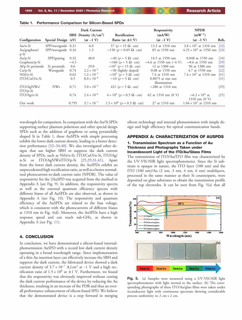
1. Transmission Spectrum as a Function of AuThickness and Photographs Taken underIncandescent Light of the ITO/Au/Glass FilmsThe transmission of ITO/Au/ITO film was characterized bythe UV-VIS-NIR light spectrophotometer. Since the Si sub-strate is opaque in nature, the ITO layer (100 nm) and theITO (100 nm)/Au (2 nm, 3 nm, 4 nm, 6 nm) multilayers,processed in the same manner as their Si counterparts, weredeposited on glass substrates to obtain the transmission profileof the top electrodes. It can be seen from Fig. 5(a) that all
Table 1. Performance Comparison for Silicon-Based SPDs
Configuration Special DesignSBH(eV)
Dark CurrentDensity (A∕cm2)
(at −1 V)Rectification
Ratio (at �1 V)
Responsivity(mA/W)(at −1 V)
NPDR(mW−1)(at −1 V) Refs.
Au/n-Si SPP/waveguide 0.31 6.0 57 (ρ ∼ 15 Ω · cm) 13.3 at 1310 nm 3.8 × 10² at 1310 nm [32]Au/graphene/p-Si
SPP/waveguide 0.34 1.3 ∼150 (ρ ∼ 0.05 Ω · cm) 85 at 1550 nm 4.25 × 10³ at 1550 nm [33]
Au/p-Si SPP/grating 0.32 48.0 ∼40 (ρ ∼ 5 Ω · cm) 14.5 at 1550 nm 0.048 at 1550 nm [34]Graphene/p-Si ∼4.5 ∼160 (ρ ∼ 5 Ω · cm) ∼4.6 at 1550 nm (−4 V) ∼8.6 at 1550 nm [39]Al/p-Si pyramids Si pyramids 0.6 29.0 ∼103 (ρ ∼ 15 Ω · cm) 12 at 1300 nm 96 at 1300 nm [40]Cu/p-Si Waveguide 0.74 2.2 × 10⁻⁵ ∼50 (lightly doped) 0.08 at 1550 nm 4.7 at 1550 nm [22]NiSi/n-Si 0.62 1.2 × 10⁻⁵ ∼105 (ρ ∼ 5 Ω · cm) 7.4 at 1310 nm 7.4 × 10² at 1310 nm [41]ITO/CuO/n-Si 0.5 8.0 × 10⁻⁶ ∼10 (ρ ∼ 5 Ω · cm) 0.0075 at one sun
illumination[31]
ITO/AgNWs/ITO/p-Si
NWs 0.71 5.0 × 10⁻⁵ 421 (ρ ∼ 5 Ω · cm) ∼280 at 1310 nm [29]
ITO/Ag/n-Si 0.74 2.4 × 10⁻⁶ 4 × 10⁵ (ρ ∼ 0.5 Ω · cm) 62 at 1310 nm (0 V) ∼6.2 × 10⁴ at1310 nm (0 V)
[25]
Our work 0.795 3.7 × 10⁻⁷ 1.5 × 10⁸ (ρ ∼ 0.5 Ω · cm) 27 at 1310 nm 1.04 × 10⁵ at 1310 nm
Fig. 5. (a) Samples were measured using a UV-VIS-NIR lightspectrophotometer with light normal to the surface. (b) The corre-sponding photographs of these ITO/Au/glass films were taken underincandescent light with continuous spectrum showing considerableprocess uniformity in 2 cm × 2 cm.
1666 Vol. 8, No. 11 / November 2020 / Photonics Research Research Article

samples show a considerable transmission over a broad wave-length range (400–1800 nm), and with the reduction of thethickness of Au film, the transmission is significantly improveddue to the increment of the incoming light. When the thicknessof Au is reduced to 2 nm, the average transmission is about80% from 850 nm to 1550 nm, and specifically, the transmis-sion can be increased to 85% for 1310 nm wavelength. Here,the increased fluctuation near 900 nm is caused by replacingthe external detector of the spectrophotometer during the test.Furthermore, the corresponding photographs of these ITO/Au/glass films in Fig. 5(b) were taken under incandescent light withcontinuous spectrum, the color of which not only reveals thereflection of the Au film but also shows the considerable processuniformity in 2 cm × 2 cm.
2. Resistivity of ITO/Au Films on GlassResistivity of ITO/Au films deposited on glass as a function ofAu thickness is shown in Fig. 6. The resistivity of only ITO filmis 4.973 × 10⁻⁴ Ω · cm, while the resistivity values of hybridITO/Au films are 4.346 × 10⁻⁴, 4.361 × 10⁻⁴, 4.532 × 10⁻⁴,and 4.508 × 10⁻⁴ Ω · cm, respectively. These results suggest thata thin Au insertion layer could slightly improve the conductivitythat may result from a better contact between Au and silicon.However, increasing Au from 2 nm to 6 nm does not signifi-cantly decrease the resistivity due to the good conductivity ofITO. In this case, the small resistivity variation of ITO/Au filmswith different Au thicknesses is probably caused by the exper-imental error of Hall measurement.
3. AFM Images and Cross-Sectional HRTEM ImagesThe RMS values of the corresponding AFM images are0.683 nm, 0.732 nm, 0.982 nm, and 1.33 nm, respectively,as shown in Fig. 7(a). As Au thickness decreases from 6 nmto 2 nm, the RMS of the electrodes is decreased from1.32 nm to 0.683 nm. Furthermore, it can be clearly seenin Fig. 7(b) that approximately 2 nm, 3 nm, 4 nm, and6 nm Au layers, respectively, are observed between ITO andn-Si, which are consistent with our design.
4. Schematic Diagram of Responsivity Measurementfor the 2AuSPDDuring the test, the Al electrode on the back of the AuSPD isadhered to the silicon substrate plated with μm thick Au layer
using conductive silver glue, and then connected with Keithley4200 through the lead wire (Al, 50 μm). As seen in Fig. 8, theeffective light receiving area under the light spot is about halfthe whole electrode except the lead wire joint. Considering thatthe effective receiving area of the detector is about one-thirdof the spot area and the light is not normally incident tothe electrode, the optical power coupled into the detectormay be lower by an order of magnitude.
5. Experimental Photocurrent for the 2AuSPD with1310 nm WavelengthThe photocurrent under 1310 nm for 2AuSPD is 2.7 × 10⁻⁶ Aat −1 V, as shown in Fig. 9. Considering the effective receivingarea and the optical power coupled into it mentioned in Fig. 8,the responsivity (R) of the whole electrode is approximately
R � IphotoP in
� 2.7 × 10⁻⁶ A2 mW∕10
× 2 � 27 mA∕W, (A1)
Fig. 8. Schematic diagram of the responsivity measurement for the2AuSPD. A 1310 nm laser with a power of 2 mW was emittedthrough a single-mode fiber with an inner diameter of 9 μm ontothe 2AuSPD arrays. The distance between the detector and the opticalfiber outlet was about 2 mm and the numerical aperture (NA) of thefiber was 0.11, leading to a spot with a diameter of 450 μm on thedetector.Fig. 6. Resistivity of ITO/Au films on glass.
Fig. 7. (a) AFM images of the top electrodes in the 2AuSPD,3AuSPD, 4AuSPD, and 6AuSPD with a scanned area of5 μm × 5 μm. (b) Cross-sectional HRTEM images of the 2AuSPD,3AuSPD, 4AuSPD, and 6AuSPD.
Research Article Vol. 8, No. 11 / November 2020 / Photonics Research 1667

where Iphoto and Pin are the photocurrent and optical powercoupled into the effective receiving area, respectively.
6. Responsivity Spectra and External QuantumEfficiency Spectra with Different Biases of AllAuSPDsThe external quantum efficiency (η) is defined as follows:
η � R · hceλ
, (A2)
where R, h, c, e, and λ are the responsivity, Planck constant,velocity of light, elementary charge, and wavelength of incidentlight, respectively. Thus, the external quantum efficiency spec-tra under different biases exhibit a similar trend as the respon-sivity spectra. As shown in Fig. 10, all the AuSPDs show thesame variation behavior of the responsivities [Fig. 10(a)] andthe external quantum efficiencies [Fig. 10(b)] under the differ-ent bias voltages. They nearly keep constant under the bias of0 V to −1 V, while they decrease a lot with the bias of 0.2 V dueto the opposite direction of the photogenerated electric fieldand the built-in electric field. All the responsivity spectra underdifferent biases exhibit two obvious absorption edges corre-sponding to the inter-band and internal photoemission, whichare the same as those in Fig. 4(c). Additionally, it can be seenfrom the responsivity spectra of different Au insertion layersthat the responsivity is inversely proportional to the thicknessof the Au layer. The responsivity increases obviously with thethinning Au layer, which mainly results from the increase of thelight transmittance of the electrode.
7. Response Time Measurement of the AuSPDs at1310 nmThe response speeds of all the AuSPDs are obtained by analyz-ing the transient response spectra, as shown in Fig. 11. TheAuSPDs are inspired by the femtosecond amplifier laser system(SOL Ace, Spectra-Physics) with 100 fs pulse width, and thewavelength was set at 1310 nm. The Tektronix TDS3054Cdigital phosphor oscilloscope (500 MHz) is used for the photo-current recorder. The response consists of a peak with full widthat half maximum of 2 ns, accompanied by a longer timescale
tail. The decay of the photocurrent can be fitted by the bi-ex-ponential Eq. (A3) as reported [42]:
I � y0 � A1 · e− tτ1 � A2 · e
− tτ2 , (A3)
where y0, A1, A2 are the pre-exponential factors and τ1, τ2 aredecay time constants, respectively. The values of τ1, τ2 with thefitting curve are 1.24 ns and 3.06 ns for 2AuSPD, 1.24 ns and
Fig. 9. Experimental photocurrent for the 2AuSPD with 1310 nmwavelength.
Fig. 10. (a) Responsivity spectra with different biases of allAuSPDs. The values of the responsivities have been calibrated witha 1310 nm laser. (b) External quantum efficiency spectra with differentbiases of all AuSPDs.
Fig. 11. Fitting of the photocurrent response curve under 0 V ofthe AuSPDs.
1668 Vol. 8, No. 11 / November 2020 / Photonics Research Research Article

2.49 ns for 3AuSPD, 0.97 ns and 2.00 ns for 4AuSPD, and1.78 ns and 4.35 ns for 6AuSPD, respectively. It can be con-cluded that the response time of all devices is on the order of ns,and the rise time is shorter from the response curve. These re-sults suggest that the response of the AuSPDs is fast enough toreach the sub-GHz response level.
Funding. National Natural Science Foundation of China(11574362, 61804176, 61991441).
Acknowledgment. The authors wish to acknowledge theassistance on the Fourier photocurrent spectrum received fromthe Key Laboratory of Semiconductor Materials Science,Institute of Semiconductors, Chinese Academy of Science.
Disclosures. The authors declare no conflicts of interest.
REFERENCES1. D. Prather, S. Shi, J. Murakowski, G. Schneider, A. Sharkawy, C.
Chen, and B. Miao, Silicon-Based Photonic Crystal Structures:From Design to Realization (Wiley, 2008), pp. 47–93.
2. D. Ahn, C.-Y. Hong, J. Liu, W. Giziewicz, M. Beals, L. Kimerling, J.Michel, J. Chen, and F. Kärtner, “High performance, waveguide inte-grated Ge photodetectors,” Opt. Express 15, 3916–3921 (2007).
3. D. Feng, S. Liao, P. Dong, N.-N. Feng, H. Liang, D. Zheng, C.-C.Kung, J. Fong, R. Shafiiha, J. Cunningham, A. Krishnamoorthy,and M. Asghari Khiavi, “High-speed Ge photodetector monolithicallyintegrated with large cross-section silicon-on-insulator waveguide,”Appl. Phys. Lett. 95, 261105 (2009).
4. A. Beling and J. C. Campbell, “InP-based high-speed photodetectors,”J. Lightwave Technol. 27, 343–355 (2009).
5. E. Peiner, A. Guttzeit, and H.-H. Wehmann, “The effect of threadingdislocations on optical absorption and electron scattering in stronglymismatched heteroepitaxial III–V compound semiconductors on sili-con,” J. Phys. Condens. Matter 14, 13195–13201 (2002).
6. Y.-T. Sun, K. Baskar, and S. Lourdudoss, “Thermal strain in indiumphosphide on silicon obtained by epitaxial lateral overgrowth,” J.Appl. Phys. 94, 2746–2748 (2003).
7. Z. Sheng, L. Liu, J. Brouckaert, S. He, and D. Thourhout, “InGaAs PINphotodetectors integrated on silicon-on-insulator waveguides,” Opt.Express 18, 1756–1761 (2010).
8. L. Pavesi, L. Negro, C. Mazzoleni, G. Franzo, and F. Priolo, “Opticalgain in Si nanocrystals,” Nature 408, 440–444 (2000).
9. J. Michel, J. Liu, and L. Kimerling, “High-performance Ge-on-Si photo-detectors,” Nat. Photonics 4, 527–534 (2010).
10. H. Meng, A. Atabaki, J. S. Orcutt, and R. J. Ram, “Sub-bandgap poly-silicon photodetector in zero-change CMOS process for telecommu-nication wavelength,” Opt. Express 23, 32643–32653 (2015).
11. T. Tanabe, H. Sumikura, H. Taniyama, A. Shinya, and M. Notomi, “All-silicon sub-Gb/s telecom detector with low dark current and highquantum efficiency on chip,” Appl. Phys. Lett. 96, 101103 (2010).
12. T. K. Liang, H. K. Tsang, I. E. Day, J. Drake, A. P. Knights, and M.Asghari, “Silicon waveguide two-photon absorption detector at 1.5 mum wavelength for autocorrelation measurements,” Appl. Phys. Lett.81, 1323–1325 (2002).
13. H. Chen and A. Poon, “Two-photon absorption photocurrent in p-i-ndiode embedded silicon microdisk resonators,” Appl. Phys. Lett. 96,191106 (2010).
14. M. Tanzid, A. Ahmadivand, R. Zhang, B. Cerjan, A. Sobhani, S. Yazdi,P. Nordlander, and N. Halas, “Combining plasmonic hot carrier gen-eration with free carrier absorption for high-performance near-infraredsilicon-based photodetection,” ACS Photon. 5, 3472–3477 (2018).
15. B. Desiatov, I. Goykhman, J. Shappir, and U. Levy, “Defect-assisted sub-bandgap avalanche photodetection in interleavedcarrier-depletion silicon waveguide for telecom band,” Appl. Phys.Lett. 104, 091105 (2014).
16. D. A. Willis and V. Grosu, “Microdroplet deposition by laser-inducedforward transfer,” Appl. Phys. Lett. 86, 244103 (2005).
17. J. Doylend, P. Jessop, and A. Knights, “Silicon photonic resonator-enhanced defect-mediated photodiode for sub-bandgap detection,”Opt. Express 18, 14671–14678 (2010).
18. H. W. Du, J. Yang, Y. H. Li, F. Xu, J. Xu, and Z. Q. Ma, “Preparation ofITO/SiOx/n-Si solar cells with non-decline potential field and hole tun-neling by magnetron sputtering,” Appl. Phys. Lett. 106, 093508(2015).
19. D. H. Shin, S. Kim, J. M. Kim, C. W. Jang, J. H. Kim, K. W. Lee, J. Kim,S. D. Oh, D. H. Lee, S. S. Kang, C. O. Kim, S. H. Choi, and K. J. Kim,“Graphene/Si-quantum-dot heterojunction diodes showing high pho-tosensitivity compatible with quantum confinement effect,” Adv. Mater.27, 2614–2620 (2015).
20. S. Y. Zhu, M. B. Yu, G. Q. Lo, and D. L. Kwong, “Near-infraredwaveguide-based nickel silicide Schottky-barrier photodetector for op-tical communications,” Appl. Phys. Lett. 92, 081103 (2008).
21. M. Casalino, G. Coppola, M. Iodice, I. Rendina, and L. Sirleto,“Critically coupled silicon Fabry-Perot photodetectors based on theinternal photoemission effect at 1550 nm,” Opt. Express 20,12599–12609 (2012).
22. M. Casalino, L. Sirleto, M. Iodice, N. Saffioti, M. Gioffre, I. Rendina,and G. Coppola, “Cu/p-Si Schottky barrier-based near infrared photo-detector integrated with a silicon-on-insulator waveguide,” Appl. Phys.Lett. 96, 241112 (2010).
23. S. Sze, Physics of Semiconductor Devices, 2nd ed. (Wiley-Interscience, 1981).
24. W. Diels, M. Steyaert, and F. Tavernier, “Schottky photodiodes in bulkCMOS for high-speed 1310/1550 nm optical receivers,” IEEE J. Sel.Top. Quantum Electron. 24, 1–8 (2018).
25. Z. Huang, Y. Mao, G. Lin, X. Yi, A. Chang, C. Li, S. Chen, W. Huang,and J. Wang, “Low dark current broadband 360–1650 nm ITO/Ag/n-Si Schottky photodetectors,” Opt. Express 26, 5827–5834(2018).
26. G.-J. Horng, C.-Y. Chang, C. Ho, C.-Y. Lee, and T. Y. Huang, “Theeffects of growth temperature on the microstructure and electricalbarrier height in PtSi/p-Si(100) Schottky barrier detector,” ThinSolid Films 374, 80–84 (2000).
27. P. Srivastava, M. Shin, K.-R. Lee, H. Mizuseki, and S. Kim, “TheSchottky barrier modulation at PtSi/Si interface by strain and structuraldeformation,” AIP Adv. 5, 087109 (2015).
28. R. T. Tung, “Recent advances in Schottky barrier concepts,” Mater.Sci. Eng. R 35, 1–138 (2001).
29. M. Patel, H. S. Kim, H. H. Park, and J. Kim, “Silver nanowires-templated metal oxide for broadband Schottky photodetector,”Appl. Phys. Lett. 108, 141904 (2016).
30. J. Yun, M. Kumar, Y. Park, H.-S. Kim, and J. Kim, “High performingITO/Ge heterojunction photodetector for broad wavelength detection,”J. Mater. Sci. Mater. Electron. 26, 6099–6106 (2015).
31. H.-S. Kim, M. D. Kumar, M. Patel, and J. Kim, “High-performing ITO/CuO/n-Si photodetector with ultrafast photoresponse,” Sens.Actuators A 252, 35–41 (2016).
32. I. Goykhman, B. Desiatov, J. Khurgin, J. Shappir, and U. Levy,“Locally oxidized silicon surface-plasmon Schottky detector for tele-com regime,” Nano Lett. 11, 2219–2224 (2011).
33. I. Goykhman, U. Sassi, B. Desiatov, N. Mazurski, S. Milana, D. Fazio,A. Eiden, J. Khurgin, J. Shappir, U. Levy, and A. Ferrari, “On-chip in-tegrated, silicon-graphene plasmonic Schottky photodetector withhigh responsivity and avalanche photogain,” Nano Lett. 16, 3005–3013 (2016).
34. M. Alavirad, A. Olivieri, L. Roy, and P. Berini, “High-responsivity sub-bandgap hot-hole plasmonic Schottky detectors,” Opt. Express 24,22544–22554 (2016).
35. X. Xu, Z. Liu, and Y. Wang, “Step-directed deposition of Au nanostruc-tures by electron beam evaporation,” J. Rare Earth 22, 141–144(2004).
36. S. K. Cheung and N.W. Cheung, “Extraction of Schottky diode param-eters from forward current‐voltage characteristics,” Appl. Phys. Lett.49, 85–87 (1986).
37. W. Mönch, “On metal-semiconductor surface barriers,” Surf. Sci. 21,443–446 (1970).
Research Article Vol. 8, No. 11 / November 2020 / Photonics Research 1669

38. Z. Huang, Y. Mao, A. Chang, H. Hong, C. Li, S. Chen, W. Huang, andJ. Wang, “Low-dark-current, high-responsivity indium-doped tin oxide/Au/n-Ge Schottky photodetectors for broadband 800–1650 nm detec-tion,” Appl. Phys. Express 11, 102203 (2018).
39. M. Amirmazlaghani, F. Raissi, O. Habibpour, J. Vukusic, and J. Stake,“Graphene-Si Schottky IR detector,” IEEE J. Quantum Electron. 49,589–594 (2013).
40. B. Desiatov, I. Goykhman, N. Mazurski, J. Shappir, J. B. Khurgin,and U. Levy, “Plasmonic enhanced silicon pyramids for internal
photoemission Schottky detectors in the near-infrared regime,”Optica 2, 335–338 (2015).
41. S. Roy, K. Midya, S. Duttagupta, and D. Ramakrishnan, “Nano-scaleNiSi and n-type silicon based Schottky barrier diode as a near infra-red detector for room temperature operation,” J. Appl. Phys. 116,124507 (2014).
42. Y. Pei, R. Pei, L. Xiaoci, Y. Wang, L. Liu, H. Chen, and J. Liang, “CdS-nanowires flexible photo-detector with Ag-nanowires electrode basedon non-transfer process,” Sci. Rep. 6, 21551 (2016).
1670 Vol. 8, No. 11 / November 2020 / Photonics Research Research Article