hts3000_55_98
TRANSCRIPT

HTS3000/HTS3000/55/9855/98
7
1-21-21-31-41-51-61-7
23456789
DVD Home Theatre System
313 978532 750

LOCATION OF PCB BOARDS
VERSION VARIATION:
1-2
STANDY PCB
CONTROL PCB
VOL PCB
TUNER PCB
MAIN PCB
POWER PCB
Type/Version
Feature & Board in used
HTS3000
/55
Main PCB ( Power Output 200W)
Power Voltage ( 120/230V )
WMA
X
X
X
X
X
X
/98
1-3
Specifi cations
AMPLIFIER
Total output power-Home Theater Mode: .................................................... 200 WFrequency Response: ....................... 180 Hz – 18 kHz / ±3 dBSignal-to-Noise Ratio: ..............................> 60 dB (A-weighted)Input Sensitivity- AUX In : ...................................................................... 500 mV- TV In: .......................................................................... 250 mV
RADIO
Tuning Range: .............................................FM 87.5–108 MHz.............................................................................. (50k/100kHz).......................................................... AM 531–1602 kHz (9kHz)........................................................ AM 530–1700 kHz (10kHz)26 dB QuietingSensitivity: ....................................... FM 22 dBf, AM 5000μV/mIF Rejection Ratio: ................................... FM 60 dB, AM 24 dBSignal-to-Noise Ratio: .............................. FM 50 dB, AM 30 dBAM Suppression Ratio: ..............................................FM 30 dBHarmonic Distortion: ............................................ FM Mono 3%............................................................................ FM Stereo 3%........................................................................................AM 5%Frequency Response ...................... FM 180 Hz–9 kHz / ±6 dBStereo Separation ......................................... FM 26 dB (1 kHz)Stereo Threshold ....................................................FM 23.5 dB
DISC
Laser Type SemiconductorDisc Diametre .........................................................12cm / 8cmVideo Decoding ........................................MPEG-1 / MPEG-2 /.............................................................................. / DivX 3/4/5/6Video DAC ..................................................................... 12 BitsSignal System ........................................................PAL / NTSCVideo Format ............................................................. 4:3 / 16:9Video S/N ...................................................... 56 dB (minimum)Composite VideoOutput ................................................................. 1.0 Vp-p, 75ΩAudio DAC ....................................................... 24 Bits / 96 kHzFrequency Response ......................... 4 Hz–20 kHz (44.1 kHz)................................................................ 4 Hz–22 kHz (48 kHz)................................................................ 4 Hz–44 kHz (96 kHz)PCM ......................................................................... IEC 60958Dolby Digital ......................................... IEC 60958, IEC 61937
MAIN UNIT
Power Supply Rating: ............................ 110-240 V~; 50-60 HzPower Consumption: ........................................................ 40 WDimensions: ....................................... 360 x 48.5 x 324.1 (mm)................................................................................... (w x h x d)Weight: ..........................................................................2.58 kg
FRONT AND REAR SPEAKERS
System: ........................................................ Full range satelliteImpedance: ..........................................................................4 ΩSpeaker drivers: ....................................... 3” full range speakerFrequency response: ...................................... 150 Hz – 20 kHzDimensions: ......................................... 100 x 95.5 x 83.5 (mm)................................................................................... (w x h x d)Weight: .................................................................0.47 kg/each
CENTRE SPEAKER
System: ........................................................ Full range satelliteImpedance: ..........................................................................8 ΩSpeaker drivers: .......................................3” full range speakerFrequency response: ...................................... 150 Hz – 20 kHzDimensions: ......................................... 100 x 95.5 x 83.5 (mm)................................................................................... (w x h x d)Weight: ..........................................................................0.52 kg
SUBWOOFER
Impedance: .......................................................................... 8 ΩSpeaker drivers: ..................................... 165 mm (6.5”) wooferFrequency response: ........................................40 Hz – 150 HzDimensions: ........................................ 131 x 386 x 315.5 (mm)................................................................................... (w x h x d)Weight: ..........................................................................3.60 kg
Specifi cations subject to change without prior notice.
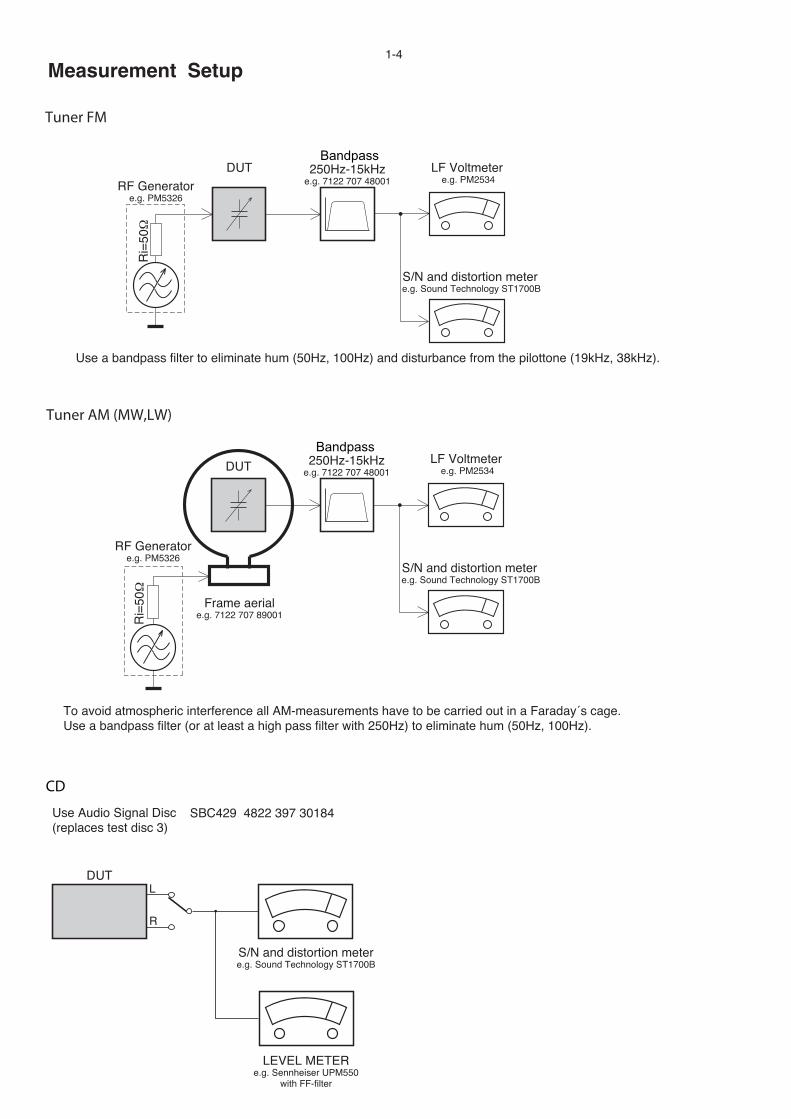
Measurement Setup
Tuner AM (MW,LW)
Tuner FM
CD
Bandpass
Bandpass
1-4

1-6
NL WAARSCHUWING
Alle IC’s en vele andere halfgeleiders zijngevoelig voor electrostatische ontladingen(ESD).Onzorgvuldig behandelen tijdens reparatie kande levensduur drastisch doen verminderen.Zorg ervoor dat u tijdens reparatie via eenpolsband met weerstand verbonden bent methetzelfde potentiaal als de massa van hetapparaat.Houd componenten en hulpmiddelen ook opditzelfde potentiaal.
I AVVERTIMENTO
Tutti IC e parecchi semi-conduttori sonosensibili alle scariche statiche (ESD).La loro longevità potrebbe essere fortementeridatta in caso di non osservazione della piùgrande cauzione alla loro manipolazione.Durante le riparazioni occorre quindi esserecollegato allo stesso potenziale che quello dellamassa dell’apparecchio tramite un braccialettoa resistenza.Assicurarsi che i componenti e anche gli utensilicon quali si lavora siano anche a questopotenziale.
GBSafety regulations require that the set be restored to its originalcondition and that parts which are identical with those specified,be used.
Safety components are marked by the symbol ! .
NL
Veiligheidsbepalingen vereisen, dat het apparaat bij reparatie inzijn oorspronkelijke toestand wordt teruggebracht en dat onderdelen,identiek aan de gespecificeerde, worden toegepast.
De Veiligheidsonderdelen zijn aangeduid met het symbol ! .
F
Les normes de sécurité exigent que l’appareil soit remis à l’étatd’origine et que soient utiliséés les piéces de rechange identiquesà celles spécifiées.
Less composants de sécurité sont marqués ! .
D
Bei jeder Reparatur sind die geltenden Sicherheitsvorschriften zubeachten. Der Original zustand des Geräts darf nicht verändert werden;für Reparaturen sind Original-Ersatzteile zu verwenden.
Sicherheitsbauteile sind durch das Symbol ! markiert.
I
Le norme di sicurezza esigono che l’apparecchio venga rimessonelle condizioni originali e che siano utilizzati i pezzi di ricambioidentici a quelli specificati.
Componenty di sicurezza sono marcati con ! .
GBAfter servicing and before returning set to customer perform a leakagecurrent measurement test from all exposed metal parts to earth groundto assure no shock hazard exist, The leakage current must notexceed 0.5mA.
CLASS 1LASER PRODUCT
3122 110 03420
GB Warning !Invisible laser radiation when open.Avoid direct exposure to beam.
S Varning !
Osynlig laserstrålning när apparaten är öppnad och spärrenär urkopplad. Betrakta ej strålen.
SF Varoitus !
Avatussa laitteessa ja suojalukituksen ohitettaessa olet alttiinanäkymättömälle laserisäteilylle. Älä katso säteeseen!
GB WARNING
All ICs and many other semi-conductors aresusceptible to electrostatic discharges (ESD).Careless handling during repair can reduce lifedrastically.When repairing, make sure that you areconnected with the same potential as the massof the set via a wrist wrap with resistance.Keep components and tools also at thispotential.
F ATTENTION
Tous les IC et beaucoup d’autressemi-conducteurs sont sensibles auxdécharges statiques (ESD).Leur longévité pourrait être considérablementécourtée par le fait qu’aucune précaution n’estprise à leur manipulation.Lors de réparations, s’assurer de bien être reliéau même potentiel que la masse de l’appareil etenfiler le bracelet serti d’une résistance desécurité.Veiller à ce que les composants ainsi que lesoutils que l’on utilise soient également à cepotentiel.
ESD
D WARNUNG
Alle ICs und viele andere Halbleiter sindempfindlich gegenüber elektrostatischenEntladungen (ESD).Unsorgfältige Behandlung im Reparaturfall kandie Lebensdauer drastisch reduzieren.Veranlassen Sie, dass Sie im Reparaturfall überein Pulsarmband mit Widerstand verbundensind mit dem gleichen Potential wie die Massedes Gerätes.Bauteile und Hilfsmittel auch auf dieses gleichePotential halten.
DK Advarse !
Usynlig laserstråling ved åbning når sikkerhedsafbrydere erude af funktion. Undgå udsaettelse for stråling.
F
"Pour votre sécurité, ces documents doivent être utilisés pardes spécialistes agréés, seuls habilités à réparer votreappareil en panne".
GB ESD PROTECTION EQUIPMENT
Complete Kit ESD3 (small tablemat, wristband,connection box, estention cable and earth cable ....... 4822 310 10671
Wristband tester ................................................................. 4822 344 13999

1-7
Pb(Lead) Free Solder
When soldering , be sure to use the pb free solder.
INDENTIFICATION:
Regardless of special logo (not always indicated)
one must treat all sets from 1 Jan 2005 onwards, according
next rules:
Important note: In fact also products of year 2004 must
be treated in this way as long as you avoid mixing solder-
alloys (leaded/ lead-free). So best to always use SAC305
and the higher temperatures belong to this.
Due to lead-free technology some rules have to be
respected by the workshop during a repair:
• Use only lead-free solder alloy Philips SAC305 with
order code 0622 149 00106. If lead-free solder-paste
is required, please contact the manufacturer of your
solder-equipment. In general use of solder-paste
within workshops should be avoided because paste is
not easy to store and to handle.
• Use only adequate solder tools applicable for lead-
free solder alloy. The solder tool must be able
– To reach at least a solder-temperature of 400°C,
– To stabilize the adjusted temperature at the solder-
tip
– To exchange solder-tips for different applications.
• Adjust your solder tool so that a temperature around
360°C – 380°C is reached and stabilized at the solder
joint. Heating-time of the solder-joint should not exceed
~ 4 sec. Avoid temperatures above 400°C otherwise
wear-out of tips will rise drastically and flux-fluid will
be destroyed. To avoid wear-out of tips switch off un-
used equipment, or reduce heat.
• Mix of lead-free solder alloy / parts with leaded solder
alloy / parts is possible but PHILIPS recommends
strongly to avoid mixed solder alloy types (leaded and
lead-free).
If one cannot avoid or does not know whether product
is lead-free, clean carefully the solder-joint from old
solder alloy and re-solder with new solder alloy
(SAC305).
• Use only original spare-parts listed in the Service-
Manuals. Not listed standard-material (commodities)
has to be purchased at external companies.
• Special information for BGA-ICs:
– Always use the 12nc-recognizable soldering
temperature profile of the specific BGA (for de-
soldering always use the lead-free temperature profile,
in case of doubt)
– Lead free BGA-ICs will be delivered in so-called ‘dry-
packaging’ (sealed pack including a silica gel pack) to
protect the IC against moisture. After opening,
dependent of MSL-level seen on indicator-label in the
bag, the BGA-IC possibly still has to be baked dry.
(MSL=Moisture Sensitivity Level). This will be
communicated via AYS-website.
Do not re-use BGAs at all.
• For sets produced before 1.1.2005 (except products
of 2004), containing leaded solder-alloy and
components, all needed spare-parts will be available
till the end of the service-period. For repair of such
sets nothing changes.
• On our website www.atyourservice.ce.Philips.com
you find more information to:
• BGA-de-/soldering (+ baking instructions)
• Heating-profiles of BGAs and other ICs used in
Philips-sets
You will find this and more technical information
within the “magazine”, chapter “workshop news”.
For additional questions please contact your local
repair-helpdesk.

2 - 12 - 1
System , Region Code , etc. Setting Produre
1)System Reset
a) press “system “ buttom on R/C,TV show “setup“
b) select the menu using the and on R/C
c) go preference page to do sysytem reset
3)Version Control Change
a) In open model, press “1“ “5“ “9“ on R/C
b) press “ok” buttom to comfi rm
c) TV will show message as below:
2)Region Code Change
a) press the “stop” buttom on R/C in open model
c) press”7” “3“ “4“ “4“ “6“ “6“ on R/C,then input desired number
to change region code :
1 USA
2 EU
3 AP
4 Australia ,NZ , Latam
5 Russia , INDIA
6 CHINA
Current model 3000-55 3000-98
Ver 00.18.00-70301-00 region : 4 / 3
Servo: OF.60.00.00
8032: 05.00.04.06 RISC:00.00.02.07
IF current model does not match you set use down arrow
key on the remote to change
4)Password Change
a) press “system “ buttom on R/C,TV show “setup“
b) select the menu using the and on R/C
c) go preference page select “password“ to change
* 000000 is default password supplied.
5)Check on the Sofeware Version
a)open the CD Door
b) press “display“ buttom on R/C
c) TV will show the version on screen
6)Upgrading new sofeware
a)open the CD Door,then insert the CD-R program disc
b)close the DOOR
c) TV will show:
“loading“
pop message“upgrading“
“writing” about 2 minutes
“done “
* the latest upgraded is in version VER 00.18.00-70301-00
C A UT ION !
T his information is c on nc ial and may notbe dis tributed. O nly a qua d s ervic epers on s hould reprogram the R egion C ode.
2 - 22 - 2
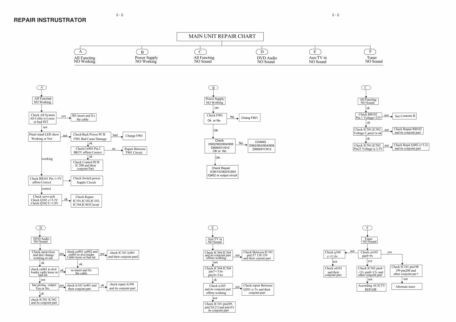
REPAIR INSTRUSTRATOR
Ok or No Chang F901
OK
Check D902/903/904/908 D909/911/912
OK or No
No
No
OK
CHANGD902/903/904/908 D909/911/912
Check Repair IC901/IC902/IC903/Q902 or output circuit
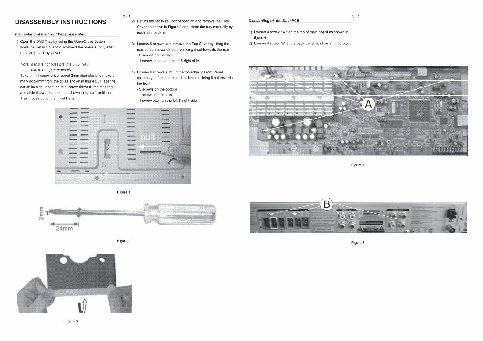
3 - 1 3 - 1
DISASSEMBLY INSTRUCTIONS
Dismantling of the Front Panel Assembly
1) Open the DVD Tray by using the Open/Close Button
while the Set is ON and disconnect the mains supply after
removing the Tray Cover.
Note: If this is not possible, the DVD Tray
has to be open manually.
Take a mini screw driver about 2mm diameter and make a
marking 24mm from the tip as shown in fi gure 2 . Place the
set on its side, insert the mini screw driver till the marking
and slide it towards the left as shown in fi gure 1 until the
Tray moves out of the Front Panel.
2) Return the set to its upright position and remove the Tray
Cover as shown in Figure 3 and close the tray manually by
pushing it back in.
3) Loosen 5 screws and remove the Top Cover by lifting the
rear portion upwards before sliding it out towards the rear.
- 3 screws on the back
- 1 screws each on the left & right side
4) Loosen 6 screws & lift up the top edge of Front Panel
assembly to free some catches before sliding it out towards
the front.
- 3 screws on the bottom
- 1 screw on the inside
- 1 screw each on the left & right side
Figure 3
Figure 2
Dismantling of the Main PCB
1) Loosen 4 screw “ A “ on the top of main board as shown in
fi gure 4.
2) Loosen 4 screw “B” at the back panel as shown in fi gure 5.
Figure 4
Figure 5
Figure 1
B
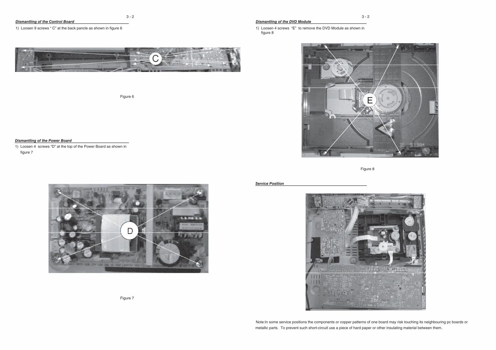
3 - 2 3 - 2Dismantling of the DVD Module
1) Loosen 4 screws “E” to remove the DVD Module as shown in fi gure 8
Dismantling of the Power Board
1) Loosen 4 screws “D” at the top of the Power Board as shown in
fi gure 7
Dismantling of the Control Board
1) Loosen 9 screws “ C” at the back pancle as shown in fi gure 6
Note:In some service positions the components or copper patterns of one board may risk touching its neighbouring pc boards or
metallic parts. To prevent such short-circuit use a piece of hard paper or other insulating material between them.
Figure 7
Figure 6
Figure 8
Service Position
4 - 14 - 1
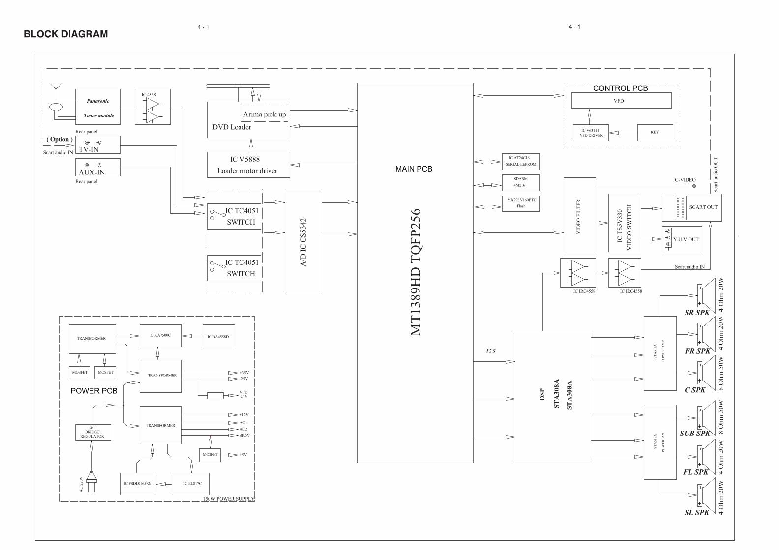
BLOCK DIAGRAM
CONTROL PCB
POWER PCB
MAIN PCB

4 - 24 - 2
WIRING DIAGRAM
TUN
ER
PC
B
MAIN PCB
DVD LOADER
POWER PCB
CONTROL PCB
VOL PCB
VFD PCB
USB PCB
MIC
/MP
3 P
CB

5 - 1 5 - 1
CONTROL BOARD
TABLE OF CONTENTS
FTD Display Pin Assignment ............................................................. 5-1
Voltage .............................................................................................. 5-2
Circuit Diagram .................................................................................. 5-3
PCB Layout Top & Bottom View ........................................................ 5-4
FTD DISPLAY PIN ASSIGNMENT

5 - 2 5 - 2
VOLTAGE
Pin NO b c eVoltage 4.7 -0.9 0
Pin NO 1 2 3 4 5 6 7 8 9 10 11 12 13 14 15 16 17 18 19 20Voltage 2.1 2.4 0 4.6 3.2 4.3 4 3.2 3.2 0 0 0 4.8 -18.9 -25.3 -25.3 -25.3 -25.3 -16.4 23.2Pin NO 21 22 23 24 25 26 27 28 29 30 31 32 33 34 35 36 37 38 39 40Voltage -16 -18.6 -1836 -20.8 -25.3 -25.3 -16.5 -18.7 -16.5 -25.4 -25.4 23.2 4.7 -25.7 -23.2 -23.2 -23.2 -23.2 -23.2 -23.2Pin NO 41 42 43 44 45 46 47 48 49 50 51 52Voltage -23.2 -23.2 -23.2 -23.2
Q200

5 - 3 5 - 3
CIRCUIT DIAGRAM
1 2 3 4
1 2 3 4
A
B
C
A
B
C
C200 A2C201 A2C202 B2C203 A2
C204 B2C205 B2C206 B2C207 B2
C208 B2C209 B2C210 B2C211 B2
C212 B2C213 C2C214 C2C215 C2
C216 B2C217 C4C218 C4C219 C1
C220 C1C221 C2C225 B3C226 B3
C288 A4C289 B4D200 C1D201 C1
D202 B1D203 C1DP200 A1FB200 B4
IC200 B1LD200 C4Q200 C3R200 A2
R201 A2R202 A2R203 A2R204 B2
R205 B2R206 C1R207 C1R208 C1
R209 C1R210 C4R211 B3R212 B2
R213 C2R214 C2R215 C2R217 B2
R218 C3R219 C3R225 C3R226 C3
RB200A A4CN203 B4RB204 B3SN200 B2
TA200 C1TA201 C1TA202 C1TA203 C1
TA204 C1TA205 C4VR200 A4XL200 B2
ZD200 A2ZD201 C4ZD202 C4ZD203 A2
ZD204 A3ZD205 B2

5 - 4 5 - 4
PCB LAYOUT - TOP VIEW
PCB LAYOUT - BOTTOM VIEW
1 2 3
1 2 3
A
B
C
A
B
C
1 2 3
1 2 3
A
B
A
B
C208 B3C209 A3C216 B1CN203 A3D200 B4D201 B4
D202 B1D203 B2DP200 B2JW1 B1JW10 B3JW11 B3
JW12 B3JW13 B3JW14 B3JW15 B3JW16 B3JW17 B4
JW18 B4JW19 B4JW2 A1JW20 B4JW21 A1JW22 A3
JW3 B1JW4 B1JW5 B1JW6 B2JW7 B2JW8 B2
JW9 B3LD200 A1R200 B3R201 B3R202 B3R203 B3
R211 B2R213 B1R214 B2R215 B1R219 B1RB200A A4
RB204 B1SN200 B3TA200 B4TA201 B4TA202 B1TA203 B4
TA204 B4TA205 A1VR200 A3XL200 B2ZD200 B3
ZD205 B2ZD204 B3ZD203 B2ZD202 A4ZD201 A4
R226 B4R225 B4R218 B4R217 B4R212 B3
R210 A4R209 B1R208 B1R207 B1R206 B4
R205 B2R204 B2Q200 B4IC200 B3FB200 A3
C289 A2 C288 A2C226 B4C225 B4C221 B1
C220 B1C219 B1C218 A4C217 A4C215 B3
C214 B4C213 B4C212 B3C211 B3C210 B2
C207 B3C206 B2C205 B3C204 B2C203 B3
C202 B2C201 B2C200 B2

6 - 1 6 - 1
MAIN BOARD
TABLE OF CONTENTS
Internal IC Diagram ........................................................................... 6-1
Circuit Diagram .................................................................................. 6-2
PCB Layout Top View ....................................................................... 6-3
PCB Layout Bottom View .................................................................. 6-4
Voltage .............................................................................................. 6-5
28 27 26 25 21222324 20 19 18 151617
MUTE
ThermalShut dowm
10k
10k
10k
10k
25k
25k
25k
15k
Vcc1
1 2 3 4 5 6 7 8 9 10 11 12 13 14
VINFC TRB-1 RSGO2 VINSL+ REGO1 FWD REV VCC1 VOTR- VOTR+ VOSL+ VOSL- VOFC- VOFC+
MUTE BLAS VINTK TRB-2 NC VINLD GND VCTL NC VCC2 VOLD- VOLD+ VOTK- VOTK+
RGND VCC1
Prc-DR V TRA Y
DRIVER
SledDriver(4X)
ActuatorDriver(6X)
SpindleDriver(4X) Driver(6X)
Actuator
Vcc2Vcc2
+-
+-
+ -
+ -
+ -
+ -
INTERNAL IC DIAGRAM - CO4558A SO8
INTERNAL IC DIAGRAM - V5888S HOSP

6 - 2 6 - 2
Circuit Diagram
1 2 3 4
1 2 3 4
A
B
C
D
A
B
C
D
C1001 D3C1002 D3C1003 D3C1004 D3C1005 D3C1006 D3C1007 D3C1008 D3C1009 D3C101 D2C1010 D3C1011 D4C1012 D3C1013 D3C1015 D4C1016 D4C1017 D4C1018 D4C1019 D4C102 D2C1020 D4C1021 D4C1022 D4C1023 D4C1024 D4C1025 D4C1026 D4C1027 D4C103 D2C110 D1C1101 B2C1102 B2C1103 B2C1104 B3 C1105 A2C1106 A2C1107 A2C1108 A3C111 D1C1110 A3C1111 A3C1112 A3C1113 A3C1114 A3C1117 A3C112 D1C113 D1C1136 C3C114 D1C116 D1C117 D1C118 D1C119 D1C120 D1C121 D1C122 D1C123 D1C124 D3C125 D3C126 D3C127 D3C128 C3C129 C3 C130 B3C131 B2C132 B2C133 C2C134 C2C135 C2C136 B2C137 B2C139 B2C140 B2C141 B2C142 B2C144 B2C157 B1C158 B1C159 B1C160 B1C162 B1C165 B1C166 B1C179 C4C180 C4C181 C4
C182 C4C183 C4C184 C4C185 C4C186 C4C188 C4C189 D1C190 C4C191 C4C193 D4C194 D4C195 C4C196 C4C197 C4C301 A1C302 A1C303 A1C304 A1C315 A1C316 A1C317 A1C318 A1C319 A1C320 A1C321 A1C322 A1C323 A1C324 A1C325 A1C326 A1C327 A1C328 A1C329 A1C330 A1C332 A1C334 A1C335 A1C336 A1C339 A2C340 A2C341 A2C342 A2C343 A2C344 A2C345 A2C346 A2C347 A2C348 A2C349 A2C350 A2C401 B3C402 B3C403 B3C404 B3C405 B3C406 B3C407 B3C408 B3C409 B3C410 B3C411 B3C412 B3C413 B3C414 B3C415 B3C416 B3C417 B3C418 B3C419 B3C420 B3C421 B3C422 B3C423 B3C425 B3C426 B3C427 B3C431 B3C432 B3C433 B3C434 B3C435 C3C436 C3C437 C3C438 C3C439 B3C440 C3
C441 C3C502 B4C504 B4C505 B4C506 B4C507 B4C508 B4C509 B4C520 B4C521 B4C523 B4C524 B4C525 B4C526 B4C527 A4C528 B4C529 B4C530 B4C533 B4C534 B4C537 B4C538 B4C539 B4C540 B4C541 B4C542 C4C544 C4C545 C4C546 C4C547 C4C548 C4C549 C4C550 B4C551 B4C553 B4C554 B4C555 B4C556 B4C557 B4C558 C4C559 B4C560 B4C563 B4C564 B4C567 B4C568 B4C569 C3C570 C3C571 C3C572 B4C573 B4C574 B4C575 B4C576 C4C577 C4C578 B4C579 B4C580 B4C581 B4C582 B4C583 B4C802 B2C803 B2C804 B2C805 C2C806 C2C807 B2C808 B2C809 B2C810 C2C811 B2C812 B2C813 B2C814 B2C815 C2C816 B2C817 B2C818 B2C819 C1C820 C1C823 C2C824 C2C825 C2C826 C2C827 C2C828 C2
C829 C2C830 C2C831 C2C833 C1C834 C1C835 C1C836 C1C838 C1C839 C1C840 C1C841 C1C842 C1C843 C1C844 C1C845 C1C846 C1C847 C2C848 C2C849 C2C850 C1C851 C1C852 C1C853 C1C854 C1C855 C1C856 D1C857 D1C858 D1CN101 D1CN103 B1CN104 B1CN801 C1CN802 D1CN803 C1D101 D1D102 D1D103 D1D104 D1D105 D1D105 D1D106 D1D107 D1D108 D1D109 D1D401 B3D402 B3D403 C3D801 C1D802 C1FB101 D2FB104 D1FB105 D1FB106 D1FB107 D1FB108 D1FB109 D1FB110 D3FB1101 A3FB1102 A2FB1103 A3FB111 D3FB1111 A3FB1112 A3FB112 C3FB113 B2FB114 B2FB115 B2FB116 B1FB121 C4FB122 C4FB123 C4FB124 C4FB125 B1FB126 B1FB127 B1FB128 D3FB401 B3FB801 B2FB802 B2FB803 C1FB804 C1FB805 D1IC101 C2IC102 C3IC103 D3IC104 D2
IC105 D3IC302 A1IC303 A1IC304 A1IC305 A2IC401 B3IC501 B4IC502 B4IC801 C1JK301A A1JK501 B4JK1103 A3JK501A B4L1101 A2L1102 A2L1103 A2L1104 A2L302 A2L307 A2L308 A2L501 B4L502 B4L503 B4L504 A4L505 C4L506 C4L507 C4L508 B4L511 B4L514 B4Q101 D1Q102 D1Q103 D1Q104 B1Q107 C3Q110 C3Q111 C3Q301 A2Q401 A3Q402 B3Q403 C3Q801 C1Q802 C1R106 D1R107 D1R108 D1R109 D1R110 D1R1101 B2R1102 B2R1103 B2R1104 B3R1105 A3R1107 A3R111 D1R1110 A3R1114 A3R112 D1R113 D1R114 D1R115 D2R117 D2R118 D2R119 D2R120 D3R121 D3R122 D3R123 D3R124 D3R125 D3R126 C3R127 C3R128 B3R129 C2R130 B2R131 B2R133 B2R134 B2R146 B1R147 B1R151 B1R152 B1R153 B1R155 B1R156 B1R157 B1
R158 B1R159 C3R160 D3R162 C4R163 C4R165 A2R166 B1 R167 B1R180 C3R181 C3R182 D2R186 C3R187 C3R188 C3R3001 A2R3002 A2R301 A1R3012 A2R302 A1R303 A1R304 A1R315 A1R316 A1R317 A1R318 A1R319 A1R320 A1R321 A1R322 A1R323 A1R324 A1R325 A1R326 A1R328 A1R329 A1R330 A1R332 A1R335 A1R336 A1R337 A1R338 A1R340 A1R342 A1R343 A2R344 A2R345 A2R346 A2R347 A2R348 A2R349 A2R350 A2R353 A2R354 A2R355 A2R357 A2R358 A2R401 B3R402 B3R403 B3R404 B3R405 B3R406 B3R407 B3R408 A3R410 B3R416 B3R418 B3R419 B3R421 B3R422 B3R423 B3R501 B4R502 B4R503 B4R505 A4R506 B4R507 B4R508 B4R509 B4R510 B4R511 B4R512 B4R514 B4R515 C4R516 C4R517 C4
R519 B4R520 B4R521 B4R522 B4R523 B4R524 B4R525 B4R526 B4R527 C4R532 B4R533 C4R801 B2R802 B2R803 C2R806 C1R807 C1R808 B2R812 C1R813 C1R814 C1R815 C2R816 C2R817 C1R818 C1R819 C1R820 C1R821 C1R822 C1R823 C1R824 C2R825 C1R826 C1R828 C1R830 C1R831 D1R832 C1R833 C1R834 D1R836 C1R837 C1R838 C1R839 C1R840 C1R841 C1R842 C1R843 C1R844 C1RA101 D3RB101 C4RB102 C4XL101 B2ZD101 B1ZD102 C4ZD104 C4ZD105 C4ZD1101 A3ZD1102 A3ZD1103 A3ZD1104 A3ZD1105 A3ZD1106 A3ZD1111 A3ZD1112 A3ZD303 A1ZD304 A1ZD305 A2ZD401 C3

6 - 3 6 - 3
PCB Layout Top View
1 2 3 4
A
B
C
1 2 3 4
A
B
C
C1111 A1C129 A1C130 A1C197 A1C315 A1C316 A1C317 A1C318 A1C321 A1C322 A1CN103 A1FB1101 A1FB1102 A1FB1111 A1FB1112 A1FB112 A1FB114 A1
FB125 A1FB126 A1FB127 A1IC302 A1JK1103 A1JK301A A1L1101 A1L1102 A1L1103 A1L1104 A1R1105 A1R1107 A1R1110 A1R1114 A1R128 A1R129 A1R151 A1
R152 A1R153 A1R155 A1R156 A1R315 A1R316 A1R317 A1R318 A1R319 A1R320 A1R322 A1R808 A1ZD1101 A1ZD1103 A1ZD1105 A1C1023 A2C123 A2
C126 A2C323 A2C324 A2C325 A2C326 A2C327 A2C328 A2C332 A2C335 A2C336 A2C439 A2D105 A2D105 A2FB1103 A2FB111 A2IC103 A2IC104 A2
IC303 A2IC304 A2Q110 A2Q111 A2R122 A2R123 A2R165 A2R180 A2R181 A2R187 A2R188 A2R301 A2R302 A2R303 A2R304 A2R323 A2R324 A2
R325 A2R326 A2R328 A2R329 A2R330 A2R332 A2R335 A2R336 A2R337 A2R338 A2R340 A2R342 A2R343 A2R344 A2R345 A2R347 A2R416 A2
RA101 A2ZD1111 A2ZD303 A2ZD304 A2C340 A3C342 A3C344 A3C346 A3C347 A3C348 A3C349 A3C402 A3C405 A3C406 A3C409 A3C410 A3C413 A3
C414 A3C415 A3C534 A3C549 A3C564 A3C583 A3D401 A3FB401 A3IC305 A3IC401 A3JK501 A3L302 A3L307 A3L308 A3L505 A3L506 A3L514 A3
Q301 A3R3001 A3R3002 A3R346 A3R348 A3R349 A3R350 A3R353 A3R354 A3R355 A3R357 A3R358 A3R401 A3R402 A3R403 A3R404 A3R405 A3
R407 A3R418 A3R419 A3R421 A3ZD305 A3C509 A4C520 A4C529 A4C530 A4C533 A4C550 A4C559 A4C560 A4C563 A4C580 A4C581 A4C582 A4
JK501A A4L501 A4L502 A4L503 A4L504 A4L507 A4L508 A4L511 A4R406 A4C132 B1C137 B1C144 B1C158 B1C159 B1C185 B1C802 B1C804 B1
C805 B1C806 B1C812 B1C813 B1C814 B1C816 B1C818 B1C819 B1C820 B1C823 B1C824 B1C825 B1C826 B1C827 B1C828 B1C830 B1C833 B1
C836 B1C838 B1C839 B1C840 B1C843 B1C846 B1CN801 B1D801 B1D802 B1FB115 B1FB116 B1FB124 B1FB801 B1FB802 B1FB803 B1FB804 B1IC101 B1
Q104 B1Q801 B1Q802 B1R130 B1R131 B1R134 B1R146 B1R147 B1R801 B1R802 B1R806 B1R807 B1R812 B1R815 B1R817 B1R818 B1R821 B1
R823 B1R836 B1R837 B1R838 B1R839 B1R840 B1R841 B1R842 B1R843 B1XL101 B1ZD101 B1C1024 B2C110 B2C113 B2C1136 B2C114 B2C124 B2
C165 B2C166 B2C184 B2C189 B2C841 B2C842 B2C845 B2CN101 B2CN104 B2CN802 B2CN803 B2D101 B2D102 B2D103 B2D104 B2D106 B2D107 B2
D108 B2D109 B2FB104 B2FB105 B2FB106 B2FB107 B2FB108 B2FB109 B2FB110 B2FB122 B2FB123 B2FB805 B2IC102 B2IC105 B2IC801 B2Q101 B2Q102 B2
Q103 B2R106 B2R107 B2R108 B2R109 B2R110 B2R111 B2R115 B2R120 B2R121 B2R126 B2R157 B2R158 B2R166 B2R167 B2R408 B2R816 B2
R819 B2R820 B2R825 B2R826 B2R828 B2R830 B2R831 B2RB101 B2C179 B3C181 B3C190 B3C196 B3C419 B3C420 B3C440 B3C441 B3C544 B3
C551 B3C570 B3C571 B3D402 B3FB121 B3IC502 B3Q107 B3Q401 B3Q402 B3Q403 B3R162 B3R163 B3R186 B3R422 B3R423 B3R517 B3ZD102 B3
ZD104 B3ZD105 B3ZD401 B3C1020 B4C502 B4C504 B4C521 B4C523 B4C524 B4C537 B4C538 B4C539 B4C540 B4C541 B4C542 B4C553 B4C554 B4
C567 B4C568 B4C569 B4IC501 B4R503 B4R505 B4R506 B4R514 B4R519 B4R520 B4R527 B4R532 B4R533 B4RB102 B4

6 - 4 6 - 4
PCB Layout Bottom View
1 2 3 4
A
B
C
1 2 3 4
A
B
C
C193 A1C194 A1C506 A1C507 A1C508 A1C526 A1C527 A1C528 A1C557 A1R501 A1
R506 A1R507 A1R508 A1R509 A1R510 A1R511 A1R512 A1R522 A1R524 A1R525 A1
R526 A1C1025 A2C304 A2C339 A2C341 A2C343 A2C345 A2C350 A2C401 A2C403 A2
C404 A2C407 A2C411 A2C412 A2C416 A2C417 A2C422 A2C423 A2C425 A2C426 A2
C427 A2R410 A2R516 A2C1010 A3C1012 A3C1016 A3C1022 A3C1117 A3C122 A3C125 A3
C301 A3C302 A3C303 A3C329 A3C330 A3C334 A3C408 A3R117 A3R118 A3R119 A3
R124 A3R125 A3ZD1112 A3C1001 A4C1004 A4C1005 A4C1008 A4C1013 A4C1015 A4C1026 A4
C1101 A4C1102 A4C1103 A4C1104 A4C1105 A4C1106 A4C1107 A4C1108 A4C1110 A4C1112 A4
C1113 A4C1114 A4C128 A4C133 A4C134 A4C162 A4C319 A4C320 A4R1101 A4R1102 A4
R1103 A4R1104 A4R127 A4R159 A4R321 A4ZD1102 A4ZD1104 A4ZD1106 A4C1011 B1C1021 B1
C431 B1C432 B1C433 B1C434 B1C505 B1C525 B1C555 B1C556 B1C558 B1C572 B1
C573 B1C574 B1C575 B1C578 B1C579 B1R502 B1R521 B1R523 B1C1018 B2C1027 B2
C180 B2C191 B2C195 B2C418 B2C421 B2C435 B2C436 B2C437 B2C438 B2C545 B2
C546 B2C547 B2C548 B2C576 B2C577 B2D403 B2R515 B2C1002 B3C1003 B3C1006 B3
C1007 B3C1017 B3C111 B3C112 B3C116 B3C117 B3C118 B3C119 B3C120 B3C121 B3
C127 B3C182 B3C183 B3C188 B3C850 B3C851 B3C852 B3C853 B3C854 B3C855 B3
C856 B3C857 B3C858 B3FB101 B3FB128 B3R112 B3R113 B3R114 B3R160 B3R182 B3
R3012 B3R832 B3R833 B3C1009 B4C101 B4C1019 B4C102 B4C103 B4C131 B4C135 B4
C136 B4C139 B4C140 B4C141 B4C142 B4C157 B4C160 B4C186 B4C803 B4C807 B4
C808 B4C809 B4C810 B4C811 B4C815 B4C817 B4C829 B4C831 B4C834 B4C835 B4
C844 B4C847 B4C848 B4C849 B4FB113 B4R133 B4R803 B4R813 B4R814 B4R822 B4
R824 B4R844 B4
6 - 5 6 - 5
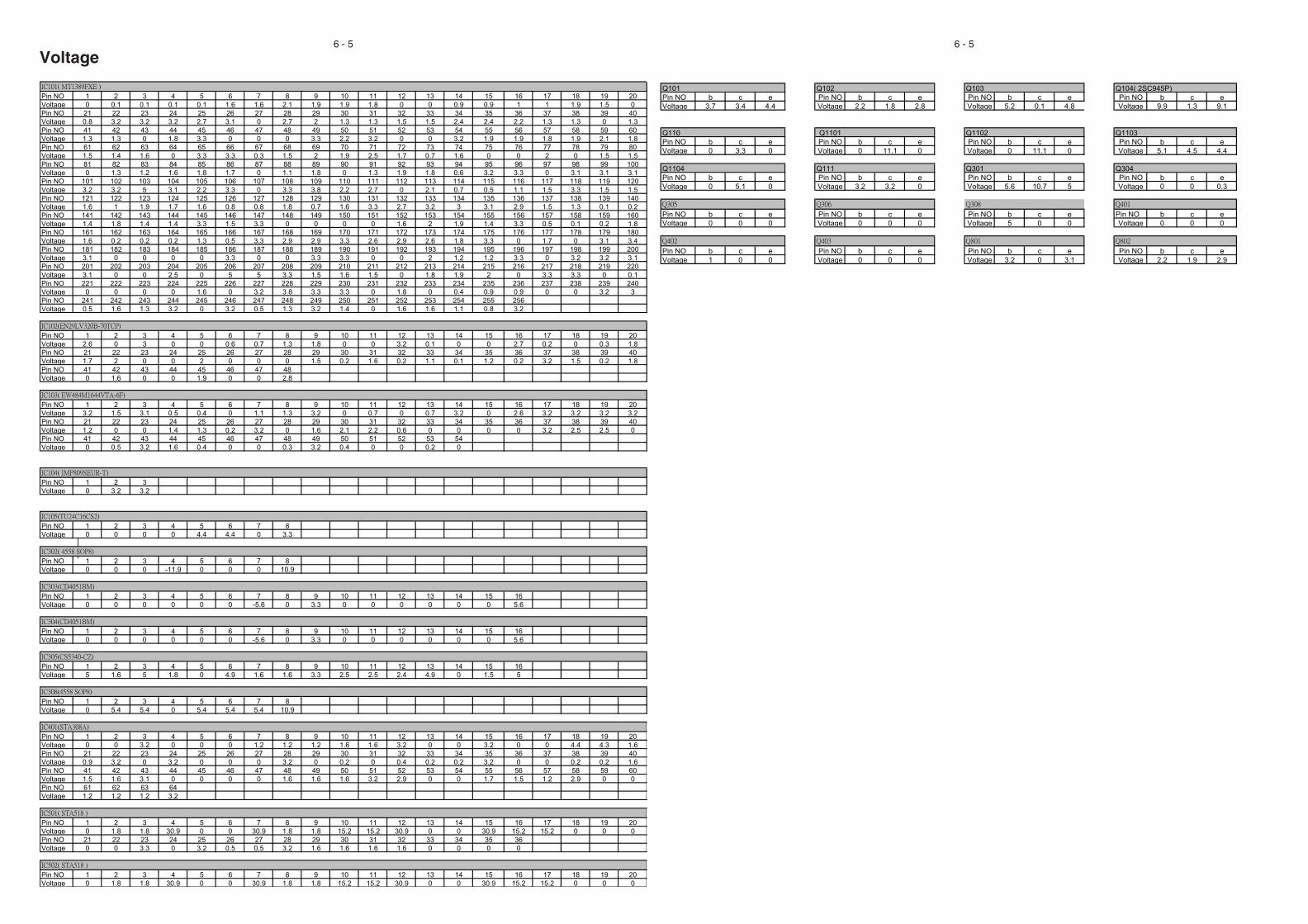
Voltage
Pin NO 1 2 3 4 5 6 7 8 9 10 11 12 13 14 15 16 17 18 19 20Voltage 0 0.1 0.1 0.1 0.1 1.6 1.6 2.1 1.9 1.9 1.8 0 0 0.9 0.9 1 1 1.9 1.5 0Pin NO 21 22 23 24 25 26 27 28 29 30 31 32 33 34 35 36 37 38 39 40Voltage 0.8 3.2 3.2 3.2 2.7 3.1 0 2.7 2 1.3 1.3 1.5 1.5 2.4 2.4 2.2 1.3 1.3 0 1.3Pin NO 41 42 43 44 45 46 47 48 49 50 51 52 53 54 55 56 57 58 59 60Voltage 1.3 1.3 0 1.8 3.3 0 0 0 3.3 2.2 3.2 0 0 3.2 1.9 1.9 1.8 1.9 2.1 1.8Pin NO 61 62 63 64 65 66 67 68 69 70 71 72 73 74 75 76 77 78 79 80Voltage 1.5 1.4 1.6 0 3.3 3.3 0.3 1.5 2 1.9 2.5 1.7 0.7 1.6 0 0 2 0 1.5 1.5Pin NO 81 82 83 84 85 86 87 88 89 90 91 92 93 94 95 96 97 98 99 100Voltage 0 1.3 1.2 1.6 1.8 1.7 0 1.1 1.8 0 1.3 1.9 1.8 0.6 3.2 3.3 0 3.1 3.1 3.1Pin NO 101 102 103 104 105 106 107 108 109 110 111 112 113 114 115 116 117 118 119 120Voltage 3.2 3.2 5 3.1 2.2 3.3 0 3.3 3.8 2.2 2.7 0 2.1 0.7 0.5 1.1 1.5 3.3 1.5 1.5Pin NO 121 122 123 124 125 126 127 128 129 130 131 132 133 134 135 136 137 138 139 140Voltage 1.6 1 1.9 1.7 1.6 0.8 0.8 1.8 0.7 1.6 3.3 2.7 3.2 3 3.1 2.9 1.5 1.3 0.1 0.2Pin NO 141 142 143 144 145 146 147 148 149 150 151 152 153 154 155 156 157 158 159 160Voltage 1.4 1.8 1.4 1.4 3.3 1.5 3.3 0 0 0 0 1.6 2 1.9 1.4 3.3 0.5 0.1 0.2 1.8Pin NO 161 162 163 164 165 166 167 168 169 170 171 172 173 174 175 176 177 178 179 180Voltage 1.6 0.2 0.2 0.2 1.3 0.5 3.3 2.9 2.9 3.3 2.6 2.9 2.6 1.8 3.3 0 1.7 0 3.1 3.4Pin NO 181 182 183 184 185 186 187 188 189 190 191 192 193 194 195 196 197 198 199 200Voltage 3.1 0 0 0 0 3.3 0 0 3.3 3.3 0 0 2 1.2 1.2 3.3 0 3.2 3.2 3.1Pin NO 201 202 203 204 205 206 207 208 209 210 211 212 213 214 215 216 217 218 219 220Voltage 3.1 0 0 2.5 0 5 5 3.3 1.5 1.6 1.5 0 1.8 1.9 2 0 3.3 3.3 0 0.1Pin NO 221 222 223 224 225 226 227 228 229 230 231 232 233 234 235 236 237 238 239 240Voltage 0 0 0 0 1.6 0 3.2 3.8 3.3 3.3 0 1.8 0 0.4 0.9 0.9 0 0 3.2 3Pin NO 241 242 243 244 245 246 247 248 249 250 251 252 253 254 255 256Voltage 0.5 1.6 1.3 3.2 0 3.2 0.5 1.3 3.2 1.4 0 1.6 1.6 1.1 0.8 3.2
Pin NO 1 2 3 4 5 6 7 8 9 10 11 12 13 14 15 16 17 18 19 20Voltage 2.6 0 3 0 0 0.6 0.7 1.3 1.8 0 0 3.2 0.1 0 0 2.7 0.2 0 0.3 1.8Pin NO 21 22 23 24 25 26 27 28 29 30 31 32 33 34 35 36 37 38 39 40Voltage 1.7 2 0 0 2 0 0 0 1.5 0.2 1.6 0.2 1.1 0.1 1.2 0.2 3.2 1.5 0.2 1.8Pin NO 41 42 43 44 45 46 47 48Voltage 0 1.6 0 0 1.9 0 0 2.8
Pin NO 1 2 3 4 5 6 7 8 9 10 11 12 13 14 15 16 17 18 19 20Voltage 3.2 1.5 3.1 0.5 0.4 0 1.1 1.3 3.2 0 0.7 0 0.7 3.2 0 2.6 3.2 3.2 3.2 3.2Pin NO 21 22 23 24 25 26 27 28 29 30 31 32 33 34 35 36 37 38 39 40Voltage 1.2 0 0 1.4 1.3 0.2 3.2 0 1.6 2.1 2.2 0.6 0 0 0 0 3.2 2.5 2.5 0Pin NO 41 42 43 44 45 46 47 48 49 50 51 52 53 54Voltage 0 0.5 3.2 1.6 0.4 0 0 0.3 3.2 0.4 0 0 0.2 0
Pin NO 1 2 3Voltage 0 3.2 3.2
Pin NO 1 2 3 4 5 6 7 8Voltage 0 0 0 0 4.4 4.4 0 3.3
Pin NO 1 2 3 4 5 6 7 8Voltage 0 0 0 -11.9 0 0 0 10.9
Pin NO 1 2 3 4 5 6 7 8 9 10 11 12 13 14 15 16Voltage 0 0 0 0 0 0 -5.6 0 3.3 0 0 0 0 0 0 5.6
Pin NO 1 2 3 4 5 6 7 8 9 10 11 12 13 14 15 16Voltage 0 0 0 0 0 0 -5.6 0 3.3 0 0 0 0 0 0 5.6
Pin NO 1 2 3 4 5 6 7 8 9 10 11 12 13 14 15 16Voltage 5 1.6 5 1.8 0 4.9 1.6 1.6 3.3 2.5 2.5 2.4 4.9 0 1.5 5
Pin NO 1 2 3 4 5 6 7 8Voltage 0 5.4 5.4 0 5.4 5.4 5.4 10.9
Pin NO 1 2 3 4 5 6 7 8 9 10 11 12 13 14 15 16 17 18 19 20Voltage 0 0 3.2 0 0 0 1.2 1.2 1.2 1.6 1.6 3.2 0 0 3.2 0 0 4.4 4.3 1.6Pin NO 21 22 23 24 25 26 27 28 29 30 31 32 33 34 35 36 37 38 39 40Voltage 0.9 3.2 0 3.2 0 0 0 3.2 0 0.2 0 0.4 0.2 0.2 3.2 0 0 0.2 0.2 1.6Pin NO 41 42 43 44 45 46 47 48 49 50 51 52 53 54 55 56 57 58 59 60Voltage 1.5 1.6 3.1 0 0 0 0 1.6 1.6 1.6 3.2 2.9 0 0 1.7 1.5 1.2 2.9 0 0Pin NO 61 62 63 64Voltage 1.2 1.2 1.2 3.2
Pin NO 1 2 3 4 5 6 7 8 9 10 11 12 13 14 15 16 17 18 19 20Voltage 0 1.8 1.8 30.9 0 0 30.9 1.8 1.8 15.2 15.2 30.9 0 0 30.9 15.2 15.2 0 0 0Pin NO 21 22 23 24 25 26 27 28 29 30 31 32 33 34 35 36Voltage 0 0 3.3 0 3.2 0.5 0.5 3.2 1.6 1.6 1.6 1.6 0 0 0 0
Pin NO 1 2 3 4 5 6 7 8 9 10 11 12 13 14 15 16 17 18 19 20Voltage 0 1.8 1.8 30.9 0 0 30.9 1.8 1.8 15.2 15.2 30.9 0 0 30.9 15.2 15.2 0 0 0
Q101 Q102 Q103 Q104( 2SC945P)Pin NO b c e Pin NO b c e Pin NO b c e Pin NO b c eVoltage 3.7 3.4 4.4 Voltage 2.2 1.8 2.8 Voltage 5.2 0.1 4.8 Voltage 9.9 1.3 9.1
Q110 Q1101 Q1102 Q1103Pin NO b c e Pin NO b c e Pin NO b c e Pin NO b c eVoltage 0 3.3 0 Voltage 0 11.1 0 Voltage 0 11.1 0 Voltage 5.1 4.5 4.4
Q1104 Q111 Q301 Q304Pin NO b c e Pin NO b c e Pin NO b c e Pin NO b c eVoltage 0 5.1 0 Voltage 3.2 3.2 0 Voltage 5.6 10.7 5 Voltage 0 0 0.3
Pin NO b c e Pin NO b c e Pin NO b c e Pin NO b c eVoltage 0 0 0 Voltage 0 0 0 Voltage 5 0 0 Voltage 0 0 0
Pin NO b c e Pin NO b c e Pin NO b c e Pin NO b c eVoltage 1 0 0 Voltage 0 0 0 Voltage 3.2 0 3.1 Voltage 2.2 1.9 2.9

7 - 1 7 - 1
POWER BOARD
TABLE OF CONTENTS
Voltage .............................................................................................. 7-1
Circuit Diagram .................................................................................. 7-2
PCB Layout Top View ....................................................................... 7-3
PCB Layout Bottom View .................................................................. 7-4
VOLTAGE
Pin NOVoltage
Pin NOVoltage
Pin NOVoltage 3.6
Pin NOVoltage
Pin NO b c e Pin NO b c e Pin NO b c e Pin NO b c eVoltage 30.5 5 31.6 Voltage -2.3 165.4 0 Voltage 33.3 -2.7 0.3 Voltage 0 30.4 0
Pin NO b c e Pin NO b c e Pin NO b c e Pin NO b c eVoltage -20.3 -1.7 -2.2 Voltage -2.3 9.2 -2.8 Voltage 0.7 0 0 Voltage 0.7 0 0
Q905 Q906 Q907 Q908
Q901 Q902 Q903 Q904

7 - 2 7 - 2
CIRCUIT DIAGRAM
1 2 3 4
1 2 3 4
A
B
C
A
B
C
BD901 A1C901 A1C902 A1C903 A2C904 A2C905 A3C907 A3C908 A4
C909 A4C910 B1C911 B1C912 B2C913 A2C914 B2C915 B3C916 A2
C917 B2C918 B3C919 A3C920 C2C921 C3C922 C3C923 B3C924 B3
C925 B3C926 B3C927 B3C928 A3C929 B3C930 B3C931 B3C932 B3
C933 A4C934 A4C935 B4C936 B1C937 C1C938 B2C939 C2C940 B1
C941 C2C942 B3C943 B3C945 B4C946 C1C947 A3C949 C2C950 C1
CN901 A4CN902 A4CN903 B4CN904 C1CN905 C3D901 A2D902 A2D903 A2
D904 B2D905 B3D908 B3D909 A3D910 B2D911 B3D912 B3D913 A4
D914 B2F901 C1GT901 B1GT902 B1GT903 B1IC901 C2IC902 B2IC903 C3
IC904 C2L901 A3L902 B3L903 B3L904 B3L905 B1NTC901 C1Q901 A3
Q902 B2Q903 B2Q904 B4Q905 B2Q906 C2Q907 C2Q908 B4Q909 C2
R901 A1R902 A2R903 A3R904 A3R905 A3R906 B3R907 B3R908 A4
R909 A1R910 A1R911 A1R912 B1R913 B2R914 B2R915 B2R916 B2
R917 C2R918 C3R919 B2R920 B2R921 A3R922 B3R923 A3R924 C2
R925 B4R926 C2R927 A3R928 A3R929 B3R930 B4R931 B4R932 B1
R934 C1R935 B1R936 B1R937 C1R939 B1R940 B2R941 B2R942 B3
R943 C3R945 C3R946 C3R947 C3R948 C2R949 C2R950 C2R951 C3
R952 B2R953 A4T901 A2TVR901 C1ZD901 B2
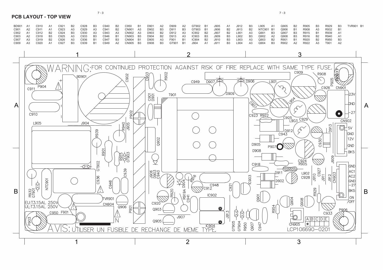
7 - 3 7 - 3
PCB LAYOUT - TOP VIEW
1 2 3
1 2 3
A
B
A
B
BD901 A1C901 A2C902 A1C903 A2C907 A3C909 A3
C910 A1C911 A1C912 B2C918 B3C919 B2C920 A1
C921 B2C923 A3C924 B3C925 A3C926 A3C927 B3
C928 B3C929 A3C930 A3C933 B3C936 B1C939 B1
C940 B2C941 B2C943 A3C946 B1C947 B3C949 A2
C950 B1CN901 A3CN902 A3CN903 B3CN904 B1CN905 B3
D901 A2D902 B3D903 B2D904 B2D905 A3D908 B3
D909 A2D911 B3D912 A3D913 A3F901 B1GT901 B1
GT902 B1GT903 B1IC902 B2IC903 B3IC904 B2J904 A1
J905 A1J906 B2J907 B2J909 B3J910 B3J911 B3
J912 B3J913 B2L901 A3L902 B3L903 A3L904 A3
L905 A1NTC901 B1Q901 B3Q902 A2Q903 B2Q904 B3
Q905 B2Q906 B1Q907 B3Q908 B3R901 B1R902 A2
R905 B3R908 A3R915 B1R916 B2R920 B2R922 A3
R929 B3R932 B1R939 A1R940 A1R950 B3T901 A2
TVR901 B1
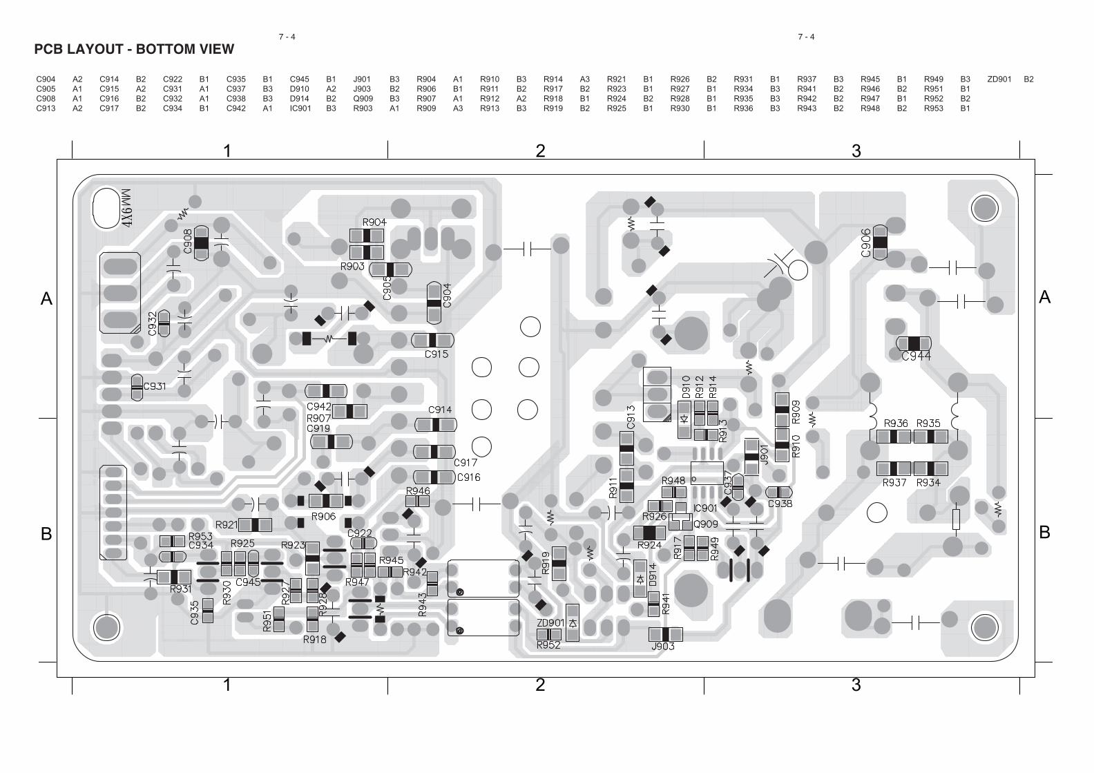
7 - 4 7 - 4
PCB LAYOUT - BOTTOM VIEW
1 2 3
A
B
1 2 3
A
B
C904 A2C905 A1C908 A1C913 A2
C914 B2C915 A2C916 B2C917 B2
C922 B1C931 A1C932 A1C934 B1
C935 B1C937 B3C938 B3C942 A1
C945 B1D910 A2D914 B2IC901 B3
J901 B3J903 B2Q909 B3R903 A1
R904 A1R906 B1R907 A1R909 A3
R910 B3R911 B2R912 A2R913 B3
R914 A3R917 B2R918 B1R919 B2
R921 B1R923 B1R924 B2R925 B1
R926 B2R927 B1R928 B1R930 B1
R931 B1R934 B3R935 B3R936 B3
R937 B3R941 B2R942 B2R943 B2
R945 B1R946 B2R947 B1R948 B2
R949 B3R951 B1R952 B2R953 B1
ZD901 B2

8 - 1
DVD BOARD
TABLE OF CONTENTS
EXPLORER VIEW ............................................................................. 8-2
MECHANICAL PART LIST ................................................................ 8-3

8 - 2
EXPLORER VIEW
8 - 3
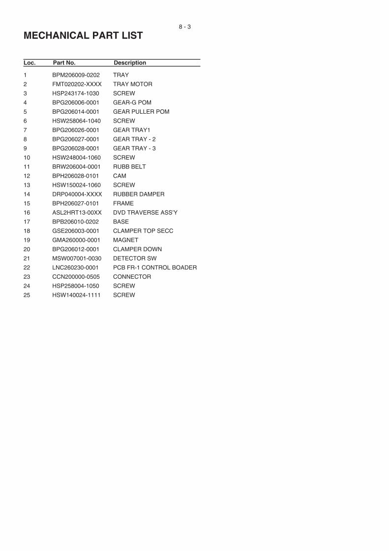
MECHANICAL PART LIST
Loc. Part No. Description
1 BPM206009-0202 TRAY
2 FMT020202-XXXX TRAY MOTOR
3 HSP243174-1030 SCREW
4 BPG206006-0001 GEAR-G POM
5 BPG206014-0001 GEAR PULLER POM
6 HSW258064-1040 SCREW
7 BPG206026-0001 GEAR TRAY1
8 BPG206027-0001 GEAR TRAY - 2
9 BPG206028-0001 GEAR TRAY - 3
10 HSW248004-1060 SCREW
11 BRW206004-0001 RUBB BELT
12 BPH206028-0101 CAM
13 HSW150024-1060 SCREW
14 DRP040004-XXXX RUBBER DAMPER
15 BPH206027-0101 FRAME
16 ASL2HRT13-00XX DVD TRAVERSE ASS’Y
17 BPB206010-0202 BASE
18 GSE206003-0001 CLAMPER TOP SECC
19 GMA260000-0001 MAGNET
20 BPG206012-0001 CLAMPER DOWN
21 MSW007001-0030 DETECTOR SW
22 LNC260230-0001 PCB FR-1 CONTROL BOADER
23 CCN200000-0505 CONNECTOR
24 HSP258004-1050 SCREW
25 HSW140024-1111 SCREW
9 - 19 - 1
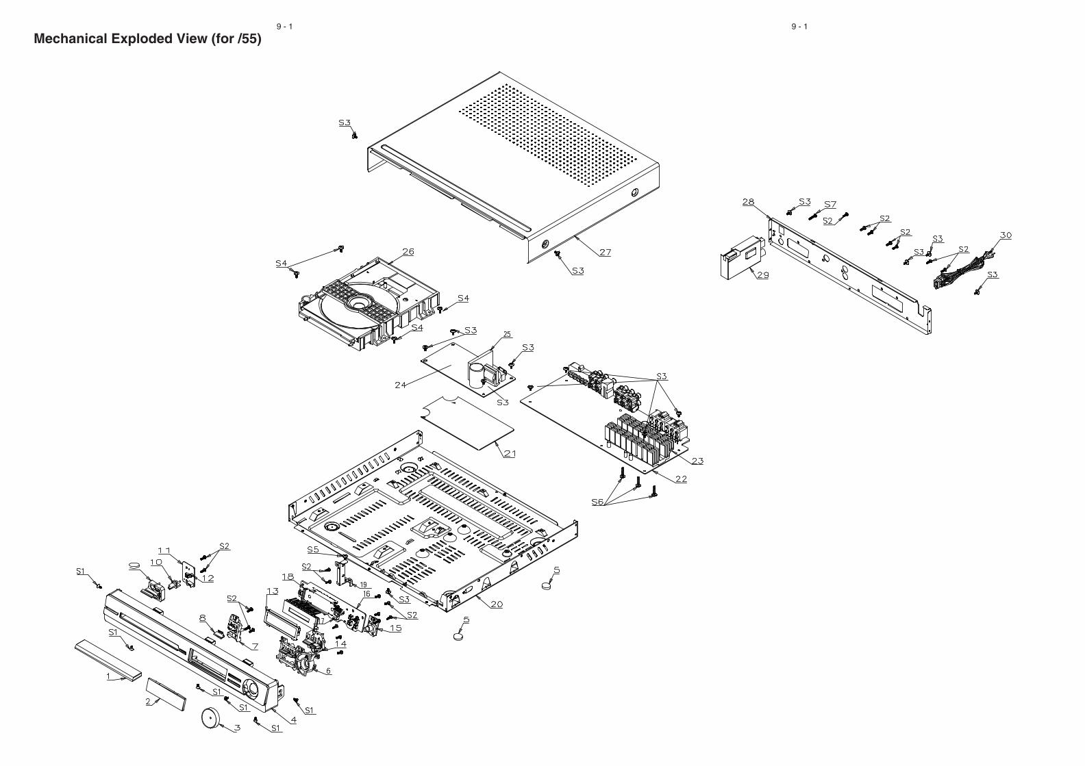
Mechanical Exploded View (for /55)

9 - 29 - 2
Mechanical Exploded View (for /98)
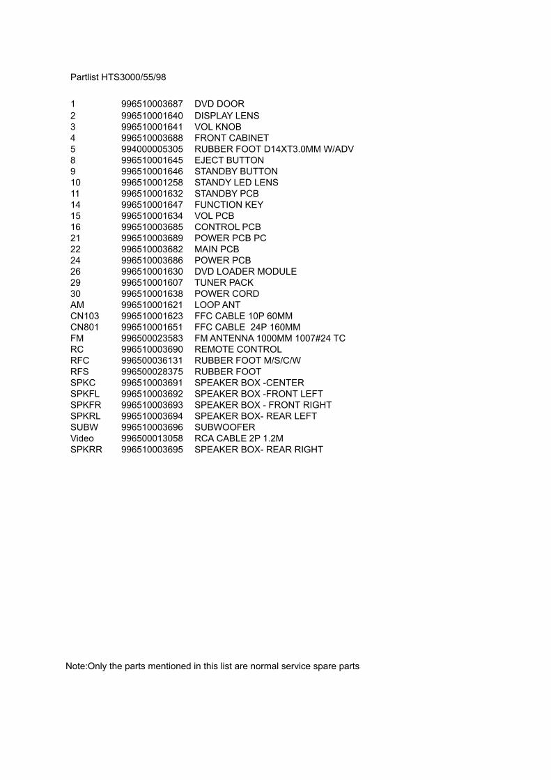
Partlist HTS3000/55/98
1 996510003687 DVD DOOR2 996510001640 DISPLAY LENS3 996510001641 VOL KNOB4 996510003688 FRONT CABINET5 994000005305 RUBBER FOOT D14XT3.0MM W/ADV8 996510001645 EJECT BUTTON9 996510001646 STANDBY BUTTON10 996510001258 STANDY LED LENS11 996510001632 STANDBY PCB14 996510001647 FUNCTION KEY15 996510001634 VOL PCB16 996510003685 CONTROL PCB21 996510003689 POWER PCB PC22 996510003682 MAIN PCB24 996510003686 POWER PCB26 996510001630 DVD LOADER MODULE29 996510001607 TUNER PACK30 996510001638 POWER CORDAM 996510001621 LOOP ANTCN103 996510001623 FFC CABLE 10P 60MMCN801 996510001651 FFC CABLE 24P 160MMFM 996500023583 FM ANTENNA 1000MM 1007#24 TCRC 996510003690 REMOTE CONTROLRFC 996500036131 RUBBER FOOT M/S/C/WRFS 996500028375 RUBBER FOOTSPKC 996510003691 SPEAKER BOX -CENTERSPKFL 996510003692 SPEAKER BOX -FRONT LEFTSPKFR 996510003693 SPEAKER BOX - FRONT RIGHTSPKRL 996510003694 SPEAKER BOX- REAR LEFTSUBW 996510003696 SUBWOOFERVideo 996500013058 RCA CABLE 2P 1.2MSPKRR 996510003695 SPEAKER BOX- REAR RIGHT
Note:Only the parts mentioned in this list are normal service spare parts