hsc-adc-evala-sc/hsc-adc-evala-dc high speed adc usb …€¦ · high speed adc usb fifo evaluation...
TRANSCRIPT
High Speed ADC USB FIFO Evaluation Kit HSC-ADC-EVALA-SC/HSC-ADC-EVALA-DC
FEATURES Buffer memory board for capturing digital data Used with high speed ADC evaluation boards 32 kB FIFO Depth at 133 MSPS (upgradeable to 256 kB) Simplifies evaluation of high speed ADCs Measures performance with ADC Analyzer™
Real-time FFT and time domain analysis Analyze SNR, SINAD, SFDR, and harmonics Import raw text data for analysis Virtual ADC eval board support using ADIsimADC™
Simple USB port interface Compatible with Windows® 98 (2nd Ed), Windows 2000, Windows Me, or Windows XP
EQUIPMENT NEEDED 3.3 V power supply Analog signal source and anti-aliasing filter Low jitter clock source High speed ADC evaluation board and ADC data sheet PC running Windows 98 (2nd Ed), Windows 2000, Windows Me, or Windows XP USB 2.0 port recommended (USB 1.1 compatible) Available ADIsimADC product model files
PRODUCT DESCRIPTION
The high speed ADC FIFO evaluation kit includes the latest version of ADC Analyzer and a memory board to capture blocks of digital data from Analog Devices’ high speed analog-to-digital converter (ADC) evaluation boards. This FIFO board can be connected to a PC through a USB port and used with ADC Analyzer to evaluate the performance of high speed ADCs quickly. Users can view an FFT for a specific analog input and encode rate and analyze SNR, SINAD, SFDR, and harmonic information.
The evaluation kit is easy to set up. Additional equipment needed includes an Analog Devices’ high speed ADC evaluation board, a power supply, a signal source, and a clock source. Once the kit is connected and powered, the evaluation is enabled instantly on the PC.
Two versions of the FIFO are available. The HSC-ADC-EVALA-DC is used with dual ADCs and converters with demultiplexed digital outputs. The HSC-ADC-EVALA-SC evaluation board is used with single-channel ADCs. See Table 1, to choose the FIFO appropriate for your high speed ADC evaluation board.
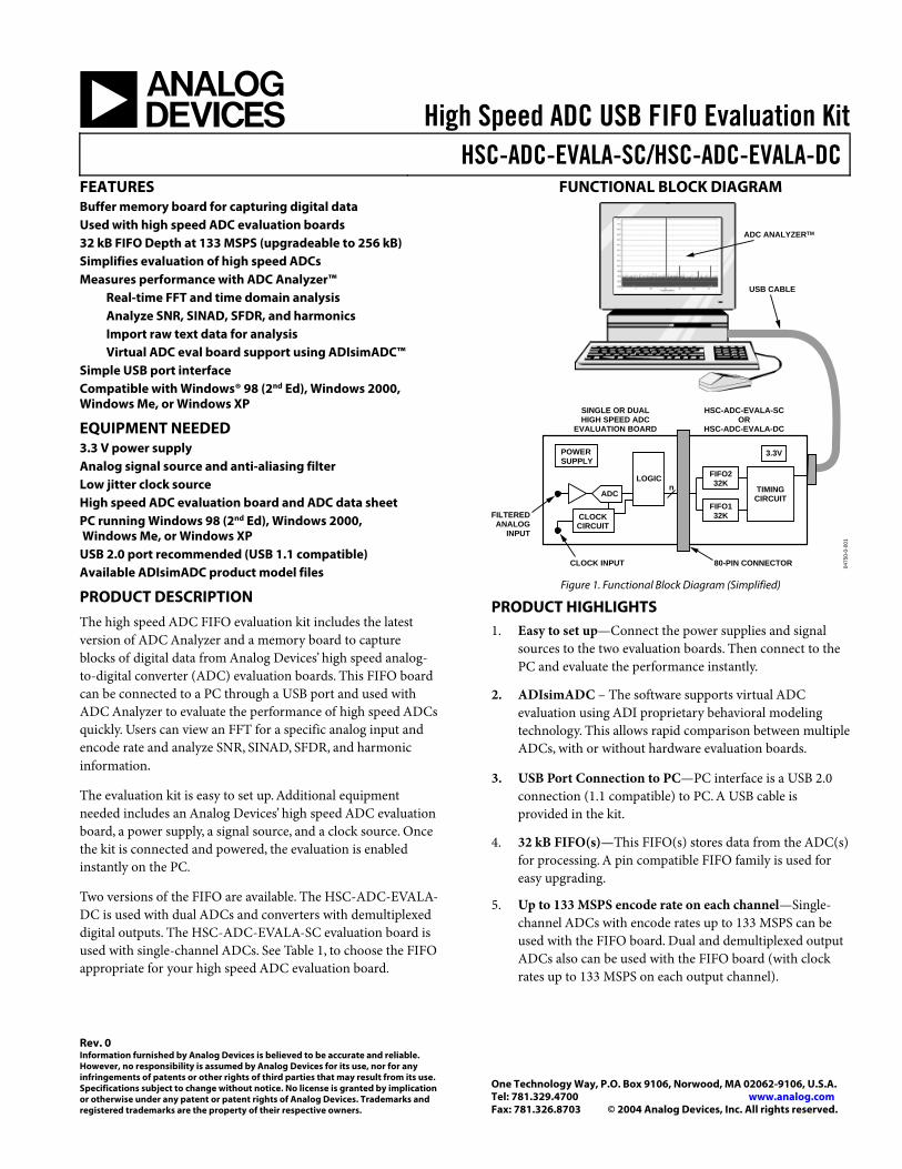
FUNCTIONAL BLOCK DIAGRAM
0475
0-0-
001
POWERSUPPLY
FIFO232K
FIFO132K
3.3V
TIMINGCIRCUITADC
n
CLOCKCIRCUIT
CLOCK INPUT
FILTEREDANALOG
INPUT
SINGLE OR DUALHIGH SPEED ADC
EVALUATION BOARD
80-PIN CONNECTOR
HSC-ADC-EVALA-SCOR
HSC-ADC-EVALA-DC
USB CABLE
ADC ANALYZERTM
LOGIC
Figure 1. Functional Block Diagram (Simplified)
PRODUCT HIGHLIGHTS 1. Easy to set up—Connect the power supplies and signal
sources to the two evaluation boards. Then connect to the PC and evaluate the performance instantly.
2. ADIsimADC – The software supports virtual ADC evaluation using ADI proprietary behavioral modeling technology. This allows rapid comparison between multiple ADCs, with or without hardware evaluation boards.
3. USB Port Connection to PC—PC interface is a USB 2.0 connection (1.1 compatible) to PC. A USB cable is provided in the kit.
4. 32 kB FIFO(s)—This FIFO(s) stores data from the ADC(s) for processing. A pin compatible FIFO family is used for easy upgrading.
5. Up to 133 MSPS encode rate on each channel—Single-channel ADCs with encode rates up to 133 MSPS can be used with the FIFO board. Dual and demultiplexed output ADCs also can be used with the FIFO board (with clock rates up to 133 MSPS on each output channel).
Rev. 0 Information furnished by Analog Devices is believed to be accurate and reliable. However, no responsibility is assumed by Analog Devices for its use, nor for any infringements of patents or other rights of third parties that may result from its use. Specifications subject to change without notice. No license is granted by implication or otherwise under any patent or patent rights of Analog Devices. Trademarks and registered trademarks are the property of their respective owners.
One Technology Way, P.O. Box 9106, Norwood, MA 02062-9106, U.S.A. Tel: 781.329.4700 www.analog.comFax: 781.326.8703 © 2004 Analog Devices, Inc. All rights reserved.
HSC-ADC-EVALA-SC/HSC-ADC-EVALA-DC
Rev. 0 | Page 2 of 44
TABLE OF CONTENTS FIFO Evaluation Board Quick Start............................................... 4
Requirements ................................................................................ 4
Quick Start Steps ...................................................................... 4
Virtual Evaluation Board Quick Start With ADIsimADC.......... 5
Requirements ................................................................................ 5
Quick Start Steps ...................................................................... 5
FIFO 4 Data Capture Board ............................................................ 6
FIFO 4 Supported ADC Evaluation Boards.............................. 6
Terminology ...................................................................................... 8
Single Tone FFT............................................................................ 8
Two-Tone FFT .............................................................................. 9
Theory of Operation ...................................................................... 10
Clocking Description................................................................. 10
Clocking with Interleaved Data................................................ 10
Installing ADC Analyzer................................................................ 11
Installation................................................................................... 11
Configuration File ...................................................................... 11
Configuring an Evaluation Board ............................................ 11
Additional Configuration Options .......................................... 14
Windowing.............................................................................. 14
Power Supply........................................................................... 14
Y-Axis....................................................................................... 14
Installing ADC Analyzer With ADIsimADC.............................. 15
Installation................................................................................... 15
Configuration File ...................................................................... 15
Configuring a Model.................................................................. 15
ADC Analyzer Functions .............................................................. 17
Time Domain.............................................................................. 17
Continuous Time Domain ........................................................ 17
FFT ............................................................................................... 17
Continuous FFT ......................................................................... 17
Average FFT ................................................................................ 17
Continuous Average FFT .......................................................... 17
Two Tone ..................................................................................... 18
Continuous Two Tone ............................................................... 18
Average Two Tone ...................................................................... 18
Stop............................................................................................... 18
Zooming and Exporting Data .................................................. 18
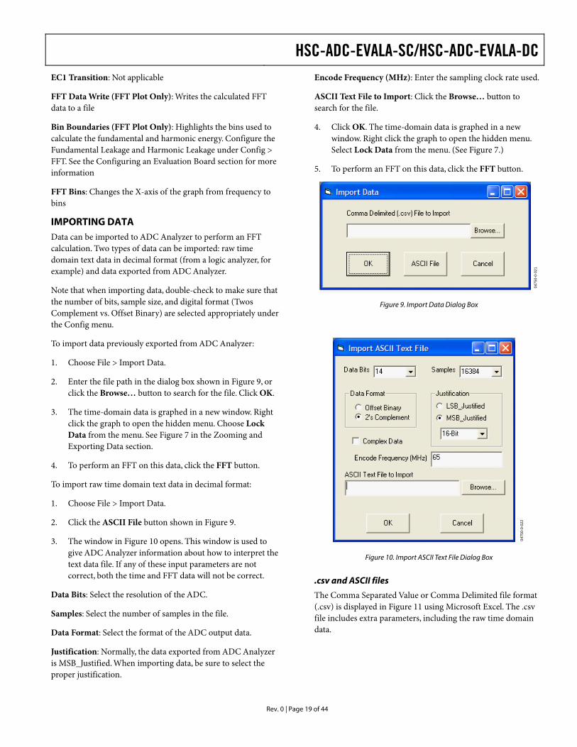
Importing Data ........................................................................... 19
.csv and ASCII files ................................................................ 19
Printing ........................................................................................ 20
Saving Files.................................................................................. 21
Additional Functions (Virtual ADC only).............................. 21
Amplitude Sweep (Virtual ADC only) .................................... 21
Analog Frequency Sweep (Virtual ADC only) ....................... 22
Troubleshooting.............................................................................. 23
Flat Line Signal Displayed......................................................... 23
Displayed Signal Unlike Analog Input .................................... 23
FFT Noise Floor Higher Than Expected................................. 24
Large Spur In FFT (Image Problem) ....................................... 24
MSBs Missing From Time Domain ......................................... 25
Upgrading FIFO Memory......................................................... 25
Jumpers ............................................................................................ 26
Default Settings........................................................................... 26
FIFO Schematices and PCB Layout ............................................. 28
FIFO Connector ......................................................................... 28
PCB Schematic............................................................................ 29
Assembly—Primary Side........................................................... 35
Assembly—Secondary Side....................................................... 36
Layer 1— Primary Side.............................................................. 37
Layer 2—Ground Plane ............................................................. 38
Layer 3—Power Plane................................................................ 39
HSC-ADC-EVALA-SC/HSC-ADC-EVALA-DC
Rev. 0 | Page 3 of 44
Layer 4—Secondary Side............................................................40
ESD Caution ................................................................................40
Bill of Materials................................................................................41
Appendix: Sampling and FFT Fundamentals..............................43
Coherent Sampling .....................................................................43
Windowing Functions................................................................43
FFT Calculations.........................................................................43
Ordering Guide ...........................................................................44
REVISION HISTORY
5/04—Revision 0: Initial Version

HSC-ADC-EVALA-SC/HSC-ADC-EVALA-DC
Rev. 0 | Page 4 of 44
FIFO EVALUATION BOARD QUICK START Install ADC Analyzer from the CD provided in the FIFO evaluation kit. See the Installing ADC Analyzer section for more details. For the latest updates to the software, check the Analog Devices website at www.analog.com/hsc-FIFO.
REQUIREMENTS Requirements include
• FIFO evaluation board, ADC Analyzer, and USB cable • High speed ADC evaluation board and ADC data sheet • 3.3 V power supply for FIFO evaluation board • Power supply for ADC evaluation board • Analog signal source and appropriate filtering • Low jitter clock source applicable for specific ADC
evaluation, typically < 1 ps rms • PC running Windows 98 (2nd Ed), Windows 2000,
Windows Me, or Windows XP • PC with a USB 2.0 port recommended (USB 1.1
compatible)
Quick Start Steps
1. Connect the FIFO evaluation board to the ADC evaluation board. If an adapter is required, insert the adapter between the ADC evaluation board and the FIFO board. If using the HSC-ADC-EVALA-SC model, connect the evaluation board to the bottom half of the 80-pin connector (closest to the installed IDT FIFO chip).
2. Connect the provided USB cable to the FIFO evaluation board and to an available USB port on the computer.
3. Refer to Table 4 for any jumper changes. Most evaluation boards can be used with the default settings.
4. After verification, connect the appropriate power supplies to the FIFO and ADC evaluation boards. The FIFO evaluation board requires a single 3.3 V power supply with 1 A current capability. Refer to the instructions included in the ADC data sheet for more information about the ADC evaluation board setup.
5. Once the cable is connected to both the computer and FIFO and power is supplied, the USB drivers start to install. To complete the total installation of the FIFO drivers, you need to complete the new hardware sequence two times. The first Found New Hardware Wizard opens with the text message This wizard helps you install software for…Pre-FIFO 4. Click the recommended install, and go to the next screen. A Hardware Installation warning window should then be displayed. Click Continue Anyway. The next window that opens should finish the Pre-FIFO 4 installation. Click Finish to complete. Your computer should go through a second Found New Hardware Wizard, and the text message, This wizard helps you install software for…Analog Devices FIFO 4, should be displayed Continue as you did in the previous installation and click Continue Anyway, then click Finish on the next two windows. This should complete the installation.
6. (Optional) Verify in the device manager that “Analog Devices, FIFO4” is listed under the USB hardware.
7. Apply power to the evaluation board and check the voltage levels at the board level.
8. Connect the appropriate analog input (which should be filtered with a band-pass filter) and low jitter clock signal. Make sure the evaluation boards are powered before connecting the analog input and clock.
9. Start ADC Analyzer (see the Installation section for installing the software).
10. Choose a configuration file for the ADC evaluation board used or create one (see the Configuring an Evaluation Board section for more information).
11. Click Time Domain (left-most button under the pull-down menus). A reconstruction of the analog input is displayed. If the expected signal does not appear, or if there is only a flat red line, refer to the Troubleshooting section for more information.
HSC-ADC-EVALA-SC/HSC-ADC-EVALA-DC
Rev. 0 | Page 5 of 44
VIRTUAL EVALUATION BOARD QUICK START WITH ADIsimADC REQUIREMENTS Requirements include
• Completed installation of ADC Analyzer version 4.5.0 or later.
• ADIsimADC product model files for the desired converter. Models are not installed with the software, but may be downloaded from the website at no charge. Go to www.analog.com/ADIsimADC or look under Design Tools for the product of interest.
• No hardware is required. However, if you wish to compare results of a real evaluation board and the model, you may switch easily between the two, as outlined below.
Quick Start Steps
1. To obtain ADC model files, go to www.analog.com/ADIsimADC or look under Design Tools for the product of interest. Download the files of interest to a local drive. The default location is c:\program files\adc_analyzer\models.
2. Start ADC Analyzer (see the Installation section for installing the software).
3. From the menu choose Config > Buffer and select Model from the drop down menu as the buffer memory. In effect, the model functions in place of the ADC and data capture hardware.
4. After selecting the Model, a small button, Model, is displayed next to the Stop button. Click Model to select and configure which converter will be modeled. This places a small form in the workspace where you can select and configure how the model will behave.
5. On the ADC Modeling form, select the Device tab and click the … button, adjacent to the dialog box. This opens a file browser and displays all of the models found in the default directory: c:\program files\adc_analyzer\models. If no model files are found, follow the on-screen directions or see Step 1 to install available models. If you have saved the models somewhere other than the default location, use the browser to navigate to that location and select the file of interest.
6. From the menu choose Config > FFT. In the FFT Configuration form, ensure that the Encode Frequency is set for a valid rate for the simulated device under test. If set too low or too high, the model will not run.
7. Once a model has been selected, information about the model displays on the Device tab. After ensuring that you have selected the right model, select the Input tab. This lets you configure the input to the model. From the drop down menu, select either Sine Wave or Two Tone for the input signal.
8. Click Time Domain (left-most button under the pull-down menus). A reconstruction of the analog input is displayed. The model may now be used just as a standard evaluation board would be.
9. The model supports additional features not found when testing a standard evaluation board. When using the modeling capabilities, it is possible to sweep either the analog amplitude or the analog frequency. See the Installing ADC Analyzer With ADISIMADC section for additional features.

HSC-ADC-EVALA-SC/HSC-ADC-EVALA-DC
Rev. 0 | Page 6 of 44
FIFO 4 DATA CAPTURE BOARD
0475
0-0-
002
IDT72V283 32K× 16-BIT FIFO
ADC EVALUATIONBOARD CONNECTION:40 PIN INTERFACE FORDATA AND CLOCK INPUTFOR TOP CHANNEL
OPTIONAL SMACLOCK INPUTS
JUMPERS TIE TOPAND BOTTOM CLOCKINPUTS TOGETHER =IN FOR SINGLECHANNEL OPTION,OUT FOR DUALCHANNEL OPTION
JUMPERS UNUSEDPINS TO GROUND
OPTIONAL FINETUNING ADJUST
ADC EVALUATIONBOARD CONNECTION:40 PIN INTERFACEFOR DATA ANDCLOCK INPUT FORBOTTOM CHANNEL
IDT72V283 32K× 16- BIT FIFO
CYPRESS F×2 HIGHSPEED USB 2.0MICROCONTROLLER
MICROCONTROLLERCRYSTAL CLOCK =24MHz. OFF DURINGDATA CAPTURE
EEPROM TO LOADUSB FIRMWARE
JUMPERS UNUSEDPINS TO GROUND
+3.3V POWERCONNECTION
INVERT WRITECLOCK OPTIONS
ADDITIONALTIMING DELAYS
FOR WRITE CLOCK
WRITE CLOCKSELECT TO
GENERATE WENSIGNAL
INVERT WRITECLOCK OPTIONS
SET WEN TIMINGFOR INTERLEAVE
MODES
USB CONNECTIONTO COMPUTER
Figure 2. FIFO Components Description
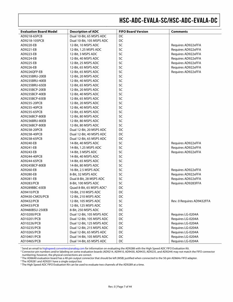
FIFO 4 SUPPORTED ADC EVALUATION BOARDS The evaluation boards in Table 1 can be used with the high speed ADC FIFO Evaluation Kit1. Some evaluation boards require an adapter between the ADC evaluation board connector and the FIFO connector. If an adapter is needed, send an email to [email protected] with the part number of the adapter and a mailing address.
Table 1 HSC-ADC-EVALA-DC: and HSC-ADC-EVALA-SC Compatible Evaluation Boards2
Evaluation Board Model Description of ADC FIFO Board Version Comments AD6640ST/PCB 12-Bit, 65 MSPS ADC SC Requires AD664xFFA3
AD6644ST/PCB 14-Bit, 65 MSPS ADC SC Rev. C Requires AD664xFFA AD6645/PCB 14-Bit, 80 MSPS ADC SC Rev. C Requires AD664xFFA AD9051/PCB 10-Bit, 60 MSPS ADC SC Requires AD9051FFA AD9057/PCB 8-Bit, 80 MSPS ADC SC Requires AD9283FFA AD9059/PCB Dual 8-Bit, 60 MSPS ADC DC Requires AD9059FFA AD9071/PCB 10-Bit, 100 MSPS ADC SC Requires AD9071FFA AD9200SSOP-EVAL 10-Bit, 20 MSPS ADC SC Requires AD922xFFA AD9200TQFP-EVAL 10-Bit, 20 MSPS ADC SC Requires AD922xFFA AD9201-EVAL Dual 10-Bit, 20 MSPS ADC4 SC Requires AD922xFFA AD9203-EB 10-Bit, 40 MSPS ADC SC Requires AD922xFFA AD9214-65PCB 10-Bit, 65 MSPS ADC SC AD9214-105PCB 10-Bit, 105 MSPS ADC SC AD9215BCP-65EB 10-Bit, 65 MSPS ADC SC AD9215BCP-80EB 10-Bit, 80 MSPS ADC SC AD9215BCP-105EB 10-Bit, 105 MSPS ADC SC AD9215BRU-65EB 10-Bit, 65 MSPS ADC SC AD9215BRU-80EB 10-Bit, 80 MSPS ADC SC AD9215BRU-105EB 10-Bit, 105 MSPS ADC SC
HSC-ADC-EVALA-SC/HSC-ADC-EVALA-DC
Rev. 0 | Page 7 of 44
Evaluation Board Model Description of ADC FIFO Board Version Comments AD9218-65PCB Dual 10-Bit, 65 MSPS ADC DC AD9218-105PCB Dual 10-Bit, 105 MSPS ADC DC AD9220-EB 12-Bit, 10 MSPS ADC SC Requires AD922xFFA AD9221-EB 12-Bit, 1.25 MSPS ADC SC Requires AD922xFFA AD9223-EB 12-Bit, 3 MSPS ADC SC Requires AD922xFFA AD9224-EB 12-Bit, 40 MSPS ADC SC Requires AD922xFFA AD9225-EB 12-Bit, 25 MSPS ADC SC Requires AD922xFFA AD9226-EB 12-Bit, 65 MSPS ADC SC Requires AD922xFFA AD9226QFP-EB 12-Bit, 65 MSPS ADC SC Requires AD922xFFA AD9235BRU-20EB 12-Bit, 20 MSPS ADC SC AD9235BRU-40EB 12-Bit, 40 MSPS ADC SC AD9235BRU-65EB 12-Bit, 65 MSPS ADC SC AD9235BCP-20EB 12-Bit, 20 MSPS ADC SC AD9235BCP-40EB 12-Bit, 40 MSPS ADC SC AD9235BCP-65EB 12-Bit, 65 MSPS ADC SC AD9235-20PCB 12-Bit, 20 MSPS ADC SC AD9235-40PCB 12-Bit, 40 MSPS ADC SC AD9235-65PCB 12-Bit, 65 MSPS ADC SC AD9236BCP-80EB 12-Bit, 80 MSPS ADC SC AD9236BRU-80EB 12-Bit, 80 MSPS ADC SC AD9236BCP-80EB 12-Bit, 80 MSPS ADC SC AD9238-20PCB Dual 12-Bit, 20 MSPS ADC DC AD9238-40PCB Dual 12-Bit, 40 MSPS ADC DC AD9238-65PCB Dual 12-Bit, 65 MSPS ADC DC AD9240-EB 14-Bit, 40 MSPS ADC SC Requires AD922xFFA AD9241-EB 14-Bit, 1.25 MSPS ADC SC Requires AD922xFFA AD9243-EB 14-Bit, 3 MSPS ADC SC Requires AD922xFFA AD9244-40PCB 14-Bit, 40 MSPS ADC SC AD9244-65PCB 14-Bit, 65 MSPS ADC SC AD9245BCP-80EB 14-Bit, 80 MSPS ADC SC AD9260-EB 16-Bit, 2.5 MSPS ADC SC Requires AD922xFFA AD9280-EB 8-Bit, 32 MSPS ADC SC Requires AD922xFFA AD9281-EB Dual 8-Bit, 28 MSPS ADC4 SC Requires AD922xFFA AD9283/PCB 8-Bit, 100 MSPS ADC SC Requires AD9283FFA AD9289BBC-65EB Quad 8-Bit, 65 MSPS ADC5 DC AD9410/PCB 10-Bit, 210 MSPS ADC DC AD9430-CMOS/PCB 12-Bit, 210 MSPS ADC DC AD9432/PCB 12-Bit, 105 MSPS ADC SC Rev. 0 Requires AD9432FFA AD9433/PCB 12-Bit, 125 MSPS ADC SC AD9480BSU-250EB 8-Bit, 250 MSPS ADC DC AD10200/PCB Dual 12-Bit, 105 MSPS ADC DC Requires LG-0204A AD10201/PCB Dual 12-Bit, 105 MSPS ADC DC Requires LG-0204A AD10226/PCB Dual 12-Bit, 125 MSPS ADC DC Requires LG-0204A AD10235/PCB Dual 12-Bit, 215 MSPS ADC DC Requires LG-0204A AD10265/PCB Dual 12-Bit, 65 MSPS ADC DC Requires LG-0204A AD10401/PCB Dual 14-Bit, 105 MSPS ADC DC Requires LG-0204A AD10465/PCB Dual 14-Bit, 65 MSPS ADC DC Requires LG-0204A 1 Send an email to [email protected] for information on evaluating the AD9288 with the High Speed ADC FIFO Evaluation Kit. 2 Connector pin numbers and/or labeling on some evaluation boards (AD9214, AD9410, AD9430, AD9433, AD9235, and AD9244) may not match the FIFO connector
numbering; however, the physical connections are correct. 3 The AD6640 evaluation board has a 40-pin output connector that should be left (MSB) justified when connected to the 50-pin AD664x FIFO adapter. 4 The AD9281 and AD9201 have a single output bus 5 The High Speed ADC FIFO Evaluation Kit can be used to evaluate two channels of the AD9289 at a time.
HSC-ADC-EVALA-SC/HSC-ADC-EVALA-DC
Rev. 0 | Page 8 of 44
TERMINOLOGY SINGLE TONE FFT
Signal-to-Noise Ratio (SNR)
The ratio of the rms signal amplitude to the rms value of the sum of all other spectral components, excluding the first five harmonics and dc. It is reported in dBc.
Signal-to-Noise Ratio Full Scale (SNRFS)
The ratio of the rms signal amplitude related to full scale (0 dB) to the rms value of the sum of all other spectral components, excluding the first five harmonics and dc. It is reported in dBFS.
User Defined Signal-to-Noise Ratio (UDSNR)
The ratio of the rms signal amplitude to the rms value of the sum of all other spectral components within a specified band set by the user, excluding harmonics and dc. It is reported in dB.
Noise Figure (NF)
The noise figure is the ratio of the noise power at the output of a device to the noise power at the input to the device, where the input noise temperature is equal to the reference temperature (273 K). The noise figure is expressed in dB.1
Signal-to-Noise-and-Distortion (SINAD)
The ratio of the rms signal amplitude to the rms value of the sum of all other spectral components, including harmonics but excluding dc. It is reported in dB.
Harmonic Distortion, Image
The ratio of the rms signal amplitude to the rms value of the nonharmonic component generated from the clocking phase difference of two ADCs, reported in dBc. Note: This measurement result is valid only when analyzing demultiplexed ADCs.
Harmonic Distortion, Second (2nd)–Sixth (6th)
The ratio of the rms signal amplitude to the rms value of the fundamental related harmonic component, reported in dBc.
Worst Other Spur (WoSpur)
The ratio of the rms signal amplitude to the rms value of the worst spurious component (excluding all harmonically related components) reported in dBc.
Total Harmonic Distortion (THD)
The rms value of the sum of all spectral harmonics specified by the user. It is reported in dBc.
Spurious-Free Dynamic Range (SFDR)
The ratio of the rms signal amplitude to the rms value of the peak spurious spectral component. The peak spurious component may or may not be a harmonic. It is reported in dBc.
Noise Floor
The rms value of the sum of all other spectral components, excluding the fundamental, its harmonics, and dc referenced to full-scale and reported in dBFS.
1For Noise Figure for an ADC, the equation is
⎟⎠⎞
⎜⎝⎛ ××
×−⎟⎠⎞
⎜⎝⎛×−−⎟⎟
⎠
⎞⎜⎜⎝
⎛×=
0.001BTklog10
2FrequencyEncodelog10SNRFS
0.001/ZVlog10FigureNoise inrms
2
k= Boltzman’s Constant = 1.38 x 10⁻²³
T = Temperature in Kelvin = 273 K B = Bandwidth = 1 Hz Encode Frequency = ADC Clock Rate Vrms = RMS Fullscale Input Voltage ZIN= Input Impedance SNRFS= FullScale ADC SNR
HSC-ADC-EVALA-SC/HSC-ADC-EVALA-DC
Rev. 0 | Page 9 of 44
TWO-TONE FFT
Two-Tone, Second Order Intermodulation Distortion Products (F1 + F2)
The resulting rms second order distortion value reported by the mixing of two analog input signals. The peak spurious component is considered an IMD product. It is reported in dBc.
Two-Tone, Second Order Intermodulation Distortion Products (F2–F1)
The resulting rms second order distortion value reported by the mixing of two analog input signals. The peak spurious component is considered an IMD product. It is reported in dBc.
Two-Tone, Third Order Intermodulation Distortion Products (2F1 + F2)
The resulting rms third order distortion value reported by the mixing of two analog input signals. The peak spurious component is considered an IMD product. It is reported in dBc.
Two-Tone, Third Order Intermodulation Distortion Products (2F2 + F1)
The resulting rms third order distortion value reported by the mixing of two analog input signals. The peak spurious component is considered an IMD product. It is reported in dBc.
Two-Tone, Worst Other Spur (WoSpur)
The resulting rms distortion value, reported by the mixing of two analog input signals that is not related to the second or third order distortion products. The peak spurious component is not considered an IMD product. It is reported in dBc.
Two-Tone, Second Order Input Intercept Point (IIP2)
The measure of full-scale input signal power of the converter minus half the IMD second order products. It is reported in dBm.
Two-Tone, Third Order Input Intercept Point (IIP3)
The measure of full-scale input signal power of the converter minus half the IMD third order products. It is reported in dBm
Two-Tone, SFDR
The ratio of the rms value of either input tone to the rms value of the peak spurious component. The peak spurious component is not an IMD product. It is reported in dBc.
.
HSC-ADC-EVALA-SC/HSC-ADC-EVALA-DC
Rev. 0 | Page 10 of 44
THEORY OF OPERATION The FIFO evaluation board can be divided into several circuits, each of which plays an important part in acquiring digital data from the ADC and allows the PC to upload and process that data. The evaluation kit is based around the IDT72V283 FIFO chip from IDT. The system can acquire digital data at speeds up to 133 MSPS and data record lengths up to 32 kB using the HSC-ADC-EVALA-SC FIFO evaluation kit. The HSC-ADC-EVALA-DC, which has two FIFO chips, is available to evaluate dual ADCs or demultiplexed data from ADCs sampling faster than 133 MSPS. A USB 2.0 microcontroller communicating with ADC Analyzer allows for easy interfacing to newer computers using the USB 2.0 (USB 1.1 compatible) interface.
The process of filling the FIFO chip(s) and reading the data back requires several steps. First, ADC Analyzer initiates the FIFO chip(s) fill process. The FIFO chip(s) are reset using a master reset signal (MRS). The USB Microcontroller then is suspended, which turns off the USB oscillator, ensuring that it does not add noise to the ADC input. After the FIFO chip(s) completely fill, the full flags from the FIFO chip(s) send a signal to the USB microcontroller to wake up the microcontroller from suspend. ADC Analyzer waits for approximately 30 ms and begins the readback process.
During the readback process, the acquisition of data from FIFO 1 (U201) or FIFO 2 (U101) is controlled via the signals OEA and OEB. Because the data outputs of both FIFO chips drive the same 16-bit data bus, the USB microcontroller controls the OEA and OEB signals to read data from the correct FIFO chip. From an application standpoint, ADC Analyzer sends commands to the USB microcontroller to initiate a read from the correct FIFO chip, or both FIFO chips in dual or interleaved mode.
CLOCKING DESCRIPTION Each channel of the buffer memory requires a clock signal to capture data. These clock signals are normally provided by the ADC evaluation board and are passed along with the data through Connector J104/204 (Pin 37 for both Channel 1 and Channel 2). If only a single clock is passed for both channels, they can be connected together by Jumper J303.
Jumpers J304 and J305 at the output of the LVDS receiver allow the output clock to be inverted by the LVDS receiver. By default, the clock outputs are inverted by the LVDS receiver.
The single-ended clock signal from each data channel is buffered and converted to a differential CMOS signal by two gates of a low voltage differential signal (LVDS) receiver, U301. This allows the clock source for each channel to be CMOS, TTL, or ECL. The clock signals are ac-coupled by 0.1 µF capacitors. Potentiometers R312 and R315 allow for fine tuning the threshold of the LVDS gates. In applications where fine-tuning
the threshold is critical, these potentiometers may be replaced with a higher resistance value to increase the adjustment range. Resistors R303, R304, R307, R308, R311, R313, R314, and R316 set the static input to each of the differential gates to a dc voltage of approximately 1.5 V.
At assembly, solder Jumpers J310–J313 are set to bypass the potentiometer. For fine adjustment using the pot, the solder jumpers must be removed.
U302, an XOR gate array, is included in the design to let users add gate delays to the FIFO memory chips clock paths. They are not required under normal conditions and are bypassed at assembly by Jumpers J314 and J315. Jumpers J306 and J307 allow the clock signals to be inverted through an XOR gate. In the default setting, the clocks are not inverted by the XOR gate.
The clock paths described above determine the WRT_CLK1 and WRT_CLK2 signals at each FIFO memory chip (U101 and U201, Pin 80). The timing options above should let you choose a clock signal that meets the setup and hold time requirements to capture valid data.
A clock generator can be applied directly to S1 and/or S3. This clock generator should be the same unit that provides the clock for the ADC. These clock paths are ac-coupled, so that a sine wave generator can be used. DC bias can be adjusted by R301/R302 and R305/R306. Note that J301 and J302 (SMA connectors) and R301, R302, R305, and R306 are not installed at the factory and must be installed by the user.
The DS90LV048A differential line receiver is used to square the clock signal levels applied externally to the FIFO evaluation board. The output of this clock receiver can either directly drive the write clock of the IDT72V283 FIFO(s), or first pass through the XOR gate timing circuitry described above.
CLOCKING WITH INTERLEAVED DATA ADCs with very high data rates may exceed the capability of a single buffer memory channel (~133 MSPS). These converters often demultiplex the data into two channels to reduce the rate required to capture the data. In these applications, ADC Analyzer must interleave the data from both channels to process it as a single channel. The user can configure the software to process the first sample from Channel 1, the second from Channel 2, and so on, or vice versa, (see the Troubleshooting section for more information). The synchronization circuit included in the buffer memory forces a small delay between the write enable signals (WENA and WENB) to the FIFO memory chips (Pin 1, U101 and U201), ensuring that the data is captured in one FIFO before the other. Jumpers J401 and J402 determine which FIFO receives WENA and which FIFO receives WENB

HSC-ADC-EVALA-SC/HSC-ADC-EVALA-DC
Rev. 0 | Page 11 of 44
INSTALLING ADC ANALYZER ADC Analyzer is designed to evaluate the performance of an Analog Devices analog-to-digital converter quickly and easily.
INSTALLATION A copy of ADC Analyzer is included on the CD that comes with the FIFO Evaluation Kit. Check the Analog Devices website for updates to the software at www.analog.com/hsc-FIFO.
1. Copy the AnalyzerSetup.exe file to the hard drive.
2. Run the setup file and follow the instructions given in the installation wizard. Note that administrator privileges are required to install the software on Windows 2000/Windows Me/Windows XP machines.
3. Once the software is installed, run the executable file (the default location is in c:\program files\ ADC_Analyzer\ADC_Analyzer.exe).
CONFIGURATION FILE A configuration file can be created for each high speed ADC evaluation board used with ADC Analyzer. A configuration file provides the software with important information about the data sent from the ADC evaluation board to the FIFO evaluation board, such as the number of bits, speed of the clock, and format of the data bits (binary or twos complement). Configuration files for some of the evaluation boards are included with the ADC Analyzer files. Each time ADC Analyzer is launched, a window opens where a configuration file can be specified. Click Yes to specify a configuration file and choose the file corresponding to the ADC being used.
The default configuration files can be modified or a new configuration file can be created using the instructions in the Configuring An Evaluation Board section.
CONFIGURING AN EVALUATION BOARD Follow Steps 1 through 5 to configure the software with the ADC evaluation board:
1. From the pull-down menus in the upper left hand corner, choose Config > DUT. The screen, DUT Configuration opens. Enter the name of the ADC being evaluated in the Device dialog box and the number of bits (resolution of the ADC) in the Number of Bits dialog box. (Note: This information is used for display purposes only.) To specify a directory different than the default to store the configuration file, enter a new location in the Default Data Directory dialog box, and click OK.
Step 1
0475
0-0-
003
2. Choose Config > FFT from the pull-down menus or right-
click any of the analysis buttons to open the FFT Configuration screen. Use this menu to configure the Fast Fourier Transform plot. If needed, modify the options under Channel A to select the appropriate channel.
Step 2
0475
0-0-
004
Note that Channel A in the software corresponds to Channel 1 on the FIFO schematics and the bottom FIFO on the evaluation

HSC-ADC-EVALA-SC/HSC-ADC-EVALA-DC
Rev. 0 | Page 12 of 44
board. Channel B corresponds to Channel 2 on the FIFO schematics and the top FIFO on the evaluation board (closest to the Analog Devices logo). See the Jumpers section for more information.
Configuring FFT— Defining Available Options
Samples: Choose the number of samples taken to calculate an FFT. The default is 16 kB samples. Users can choose more or fewer samples, depending on the application. The maximum number of samples that can be selected in the software is 64 kB. However, the FIFO evaluation boards are configured with 32 kB FIFOs. For single ADCs evaluated with the HSC-ADC-EVALA-SC model, the maximum number of samples selected should match the FIFO memory on the evaluation board. For dual ADCs evaluated with the HSC-ADC-EVALA-DC model, the maximum number of samples should match the FIFO memory of each channel (a different number of samples can be selected for each channel). ADCs with demultiplexed outputs (such as the AD9430) can be used with a sample value of twice the FIFO memory. See the Upgrading FIFO Memory section.
Averages: Specify the number of averages taken for the average FFT functions. See the ADC Analyzer Functions section for more information.
Encode Frequency (MHz): Enter the speed of the sampling clock to the ADC. If evaluating a dual ADC, two different clock rates can be entered. Note: If the value is wrong, the analog fundamental frequency displayed will be wrong.
FullScale Input Power (dBm): This feature lets the user enter the amount of power (in dBm) needed on the input to determine the output fullscale. It applies only in noise figure and IIP2/IIP3 calculations.
Enable Fundamental Override: ADC Analyzer automatically defaults the highest spur as the fundamental frequency of interest. However, in some applications, the user may have a very small analog input signal that could be equal to or below another spurious harmonic. This option lets the user specify the small analog input signal needed for evaluation. If Enable Fundamental Override is checked, the Fundamental Frequency (MHz) box is enabled for the user to specify.
Fundamental Leakage: The number of bins that are neglected on either side of the fundamental signal when calculating the SNR and SINAD results. For example, if an encode rate is defined at 80 MSPS with 16384 samples, then 80M/21/(16384/21) = 4883 Hz/Bin is specified. The type of windowing selected determines the default value of the fundamental leakage. See the Windowing section for more information. The default values are 25, 10, and 1 for Hanning, Blackman Harris, and no windowing, respectively.
Harmonic Leakage: The number of bins that are neglected on either side of each harmonic of the fundamental signal defined
in the Max # of Harmonics’ box. Typically, this can be left at the default value of 3.
DC Leakage: The number of bins (at dc) that are not used in calculating SNR and SINAD. Typically, this can be left at the default value of 6.
Maximum Number of Harmonics: The number of harmonics displayed by ADC Analyzer. The default value is 6 and the maximum number of harmonics that can be displayed is 12.
Twos Complement: Check this box if the data from the ADC evaluation board is in twos complement format. Refer to the ADC data sheet to determine if the ADC outputs are configured for twos complement or offset binary. If the Twos Complement option is not checked, ADC Analyzer will expect the data outputs from the ADC to be in offset binary format.
User Defined SNR Left (MHz): This is the amount of frequency specified to the left of the fundamental by the user to analyze SNR. The resulting value is called UDSNR and will show up after an FFT plot is captured.
User Defined SNR Right (MHz): This is the amount of frequency specified to the right of the fundamental by the user to analyze SNR. The resulting value is called UDSNR and will show up after an FFT plot is captured.
After configuring the options for the Fast Fourier Transform plot in this window, click OK.
3. Choose Config > Buffer. HSC-ADC-EVAL(A), opening the Buffer Memory screen.
Step 3
0475
0-0-
005
Click OK, and the Buffer Configuration window opens. ADC Analyzer automatically seeks a USB connection. If a USB connection is not found, it will assume that you want to use an older version FIFO board which has a parallel connection. If so, choose the appropriate parallel connection made to the computer and click OK.

HSC-ADC-EVALA-SC/HSC-ADC-EVALA-DC
Rev. 0 | Page 13 of 44
Step 3a
0475
0-0-
006
4. Choose Config > Bits > Data Bits to open the Bit Mask screen. Configure the number and location of the data bits used to calculate the FFTs.
Make sure that the number of bits matches the resolution of the converter. All of the supported evaluation boards are MSB justified, so check the number of bits for the converter starting with Bit 15 (MSB). Exceptions to this are the AD9280, AD9281, AD9200, and AD9201. For these four ADCs, check the number of bits starting with Bit 13.
If a single ADC is being evaluated, check only Channel A and the appropriate bits under Channel A. If a dual ADC is being evaluated, check Channel A and Channel B on the Channel Select screen. (Config > Channel Select).
Step 4
0475
0-0-
007
If evaluating a demultiplexed ADC, go to Config > Channel Select, opening the Channel Select pop-up menu, and check the Interleaved Data box. This automatically selects both Channel A and Channel B. When using a dual ADC, select only the appropriate channel that corresponds to the ADC that is being evaluated. Channel A is the default selected channel at startup.
Step 4a
0475
0-0-
008
Note that Channel A in the software corresponds to Channel 1 on the FIFO schematics and the bottom FIFO (U201) on the

HSC-ADC-EVALA-SC/HSC-ADC-EVALA-DC
Rev. 0 | Page 14 of 44
evaluation board. Channel B corresponds to Channel 2 on the FIFO schematics and the top FIFO (U101) on the evaluation board (closest to the Analog Devices logo). See the Jumpers section for more information. Click OK. (For more information about the channel selection process, see the Troubleshooting section.)
5. As a last step, choose File > Configuration File > Save Configuration from the pull-down menu to save the configuration for future use. Choose a file name and a location to save the file.
ADDITIONAL CONFIGURATION OPTIONS Other options under the configuration pull-down menu include Windowing, Power Supply, and Y-Axis.
Windowing
Choose either the Hanning or Blackman Harris (default) windowing functions or turn windowing off. See the Windowing Functions section for a description of Hanning and Blackman Harris windowing. Click OK.
0475
0-0-
009
Figure 3. Select Windowing Function
If you choose None, the Coherent Sampling Calculator window opens (see Figure 4).
0475
0-0-
010
Figure 4. Coherent Sampling Calculator
For the calculator to work properly, the correct sampling frequency must be entered under Config > FFT. Select either the desired approximate Analog Input Frequency or the # of Sine Wave Cycles. Enter the value in the dialog box (not labeled) and click Calculate to view the Coherent Frequency. The Coherent Frequency and Number of Integer Cycles will display in the gray boxes. Click OK to exit the Coherent Sampling Calculator.
Power Supply
This option opens under Config > Power Supply, and users can enter the value of the ADC analog and digital voltage supplies (see Figure 5). Note this for user documentation only. No external control is provided. ADC Analyzer displays this information when data is captured. See the ADC Analyzer Functions section for more information.
0475
0-0-
011
Figure 5. Power Supply Configuration
Y-Axis
Use the Y Axis screen to configure the display of the FFT Y-Axis. Go to Config > YAxis to change the default value of –130, which is a typical setting for the noise floor of a 14-bit ADC with 16,384 samples in the FFT calculation.
0475
0-0-
012
Figure 6. Y Axis Configuration
HSC-ADC-EVALA-SC/HSC-ADC-EVALA-DC
Rev. 0 | Page 15 of 44
INSTALLING ADC ANALYZER WITH ADIsimADC ADC Analyzer is useful also as an evaluation tool for simulated ADCs using ADIsimADC.
INSTALLATION The simulation tools are installed as part of the regular installation of ADC Analyzer (for instructions, see the Installing ADC Analyzer section). Before using these features, the desired model files must be installed. Locate the available models on the Analog Devices website www.analog.com/ADIsimADC or by locating the desired converter product and going to the Design Tools area for that product.
1. Download the desired model file to the models directory. The default is c:\program files\adc_analyzer\models.
2. Although the software is provided with the evaluation board, no hardware is required to use the modeling software. Updates to the software are posted periodically to www.analog.com as well as new and updated models. Check the website frequently to ensure that you have the latest for both files.
3. Once the software and models are installed, run the executable file (the default location is in c:\program files\adc_analyzer\adc_analyzer.exe.
CONFIGURATION FILE As with using an ADC evaluation board, a corresponding configuration file must be loaded before simulations can occur. This file provides the software with important information about the format in which the data is generated, and other information, such as the number of bits, speed of the clock, and format of the data bits (binary or twos complement). Configuration files for some of the evaluation boards are included with the ADC Analyzer files. Each time ADC Analyzer is launched, a window opens in which a configuration file can be specified. Click Yes to specify a configuration file and choose the file corresponding to the ADC evaluation board being used. For more details, see the Configuring an Evaluation Board section.
CONFIGURING A MODEL To configure the software for use with ADIsimADC virtual evaluation board, follow Steps 1 through 8.
1. Choose Config > FFT from the pull-down menus or right-click on any of the analysis buttons to bring up the FFT Configuration menu. In this window, set the encode rate to the desired rate that the converter can support. If an encode rate is specified outside the operating range of the converter, the model will not function as expected and erroneous results will be obtained. Make any other adjustments necessary. If you have questions, see the Configuring an Evaluation Board. Click OK when finished.
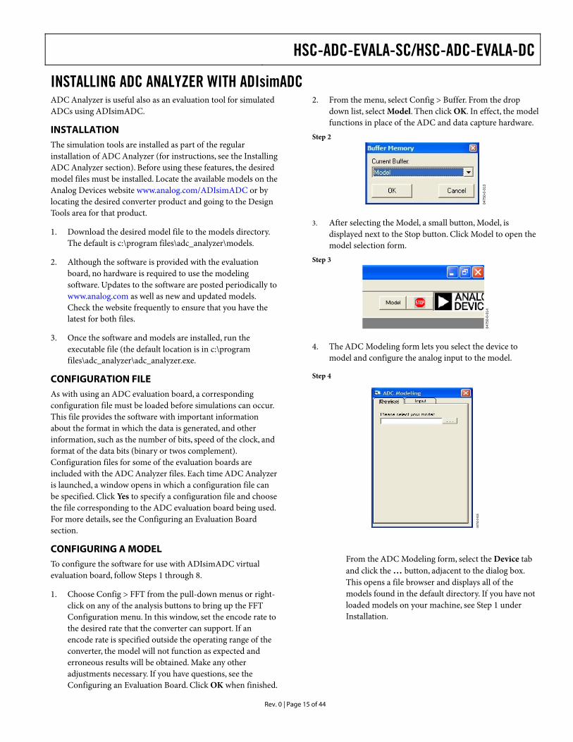
2. From the menu, select Config > Buffer. From the drop down list, select Model. Then click OK. In effect, the model functions in place of the ADC and data capture hardware.
Step 2
0475
0-0-
013
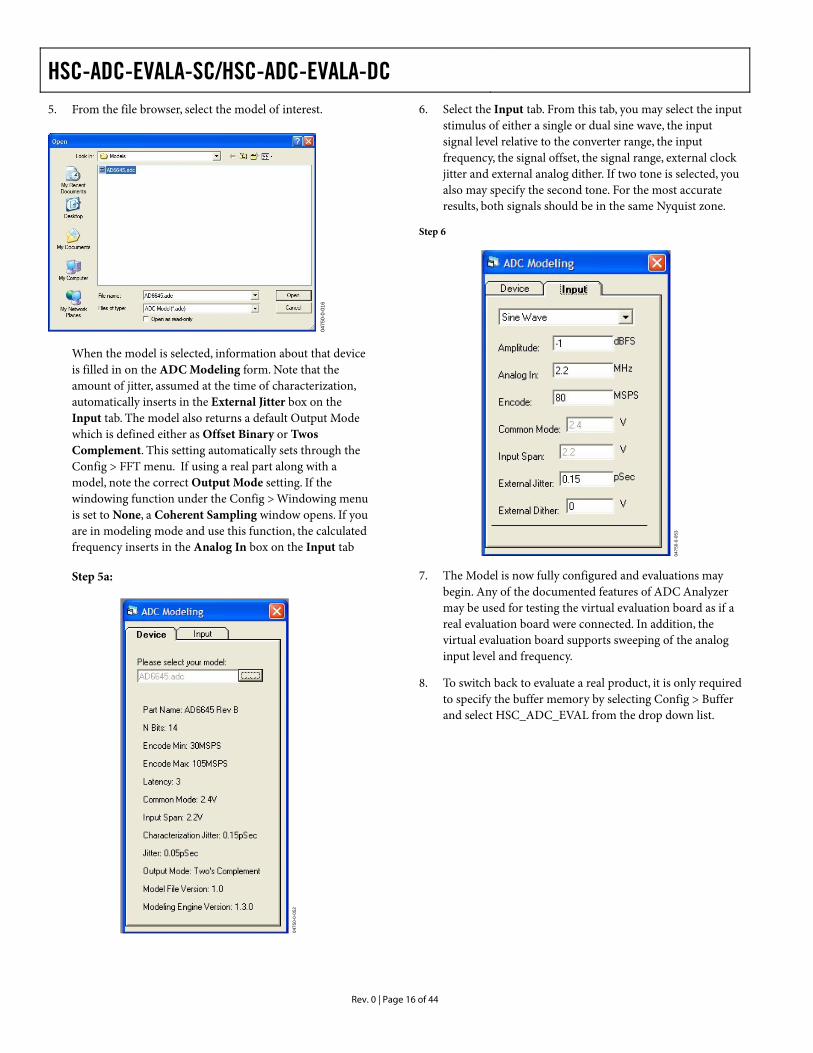
3. After selecting the Model, a small button, Model, is displayed next to the Stop button. Click Model to open the model selection form.
Step 3
0475
0-0-
014
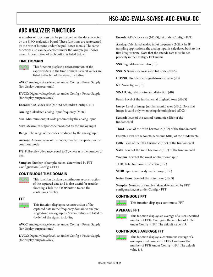
4. The ADC Modeling form lets you select the device to model and configure the analog input to the model.
Step 4
0475
0-0-
015
From the ADC Modeling form, select the Device tab and click the … button, adjacent to the dialog box. This opens a file browser and displays all of the models found in the default directory. If you have not loaded models on your machine, see Step 1 under Installation.
HSC-ADC-EVALA-SC/HSC-ADC-EVALA-DC
Rev. 0 | Page 16 of 44
5. From the file browser, select the model of interest.
0475
0-0-
016
When the model is selected, information about that device is filled in on the ADC Modeling form. Note that the amount of jitter, assumed at the time of characterization, automatically inserts in the External Jitter box on the Input tab. The model also returns a default Output Mode which is defined either as Offset Binary or Twos Complement. This setting automatically sets through the Config > FFT menu. If using a real part along with a model, note the correct Output Mode setting. If the windowing function under the Config > Windowing menu is set to None, a Coherent Sampling window opens. If you are in modeling mode and use this function, the calculated frequency inserts in the Analog In box on the Input tab
Step 5a:
0475
0-0-
052
6. Select the Input tab. From this tab, you may select the input stimulus of either a single or dual sine wave, the input signal level relative to the converter range, the input frequency, the signal offset, the signal range, external clock jitter and external analog dither. If two tone is selected, you also may specify the second tone. For the most accurate results, both signals should be in the same Nyquist zone.
Step 6
0475
0-0-
053
7. The Model is now fully configured and evaluations may begin. Any of the documented features of ADC Analyzer may be used for testing the virtual evaluation board as if a real evaluation board were connected. In addition, the virtual evaluation board supports sweeping of the analog input level and frequency.
8. To switch back to evaluate a real product, it is only required to specify the buffer memory by selecting Config > Buffer and select HSC_ADC_EVAL from the drop down list.
HSC-ADC-EVALA-SC/HSC-ADC-EVALA-DC
Rev. 0 | Page 17 of 44
ADC ANALYZER FUNCTIONS A number of functions can be performed on the data collected by the FIFO evaluation board. These functions are represented by the row of buttons under the pull-down menus. The same functions also can be accessed under the Analyze pull-down menu. A description of each button is listed below.
TIME DOMAIN
This function displays a reconstruction of the captured data in the time domain. Several values are listed to the left of the signal, including
AVCC: Analog voltage level, set under Config > Power Supply (for display purposes only)
DVCC: Digital voltage level, set under Config > Power Supply (for display purposes only)
Encode: ADC clock rate (MSPS), set under Config > FFT
Analog: Calculated analog input frequency (MHz)
Min: Minimum output code produced by the analog input
Max: Maximum output code produced by the analog input
Range: The range of the codes produced by the analog input
Average: Average value of the codes; may be interpreted as the common mode
F/S: Full-scale code range, equal to 2n, where n is the number of bits
Samples: Number of samples taken, determined by FFT Configuration (Config > FFT)
CONTINUOUS TIME DOMAIN
This function displays a continuous reconstruction of the captured data and is also useful for trouble–shooting. Click the STOP button to end the continuous display.
FFT
This function displays a reconstruction of the captured data in the frequency domain to analyze single-tone analog inputs. Several values are listed to the left of the signal, including
AVCC: Analog voltage level, set under Config > Power Supply (for display purposes only)
DVCC: Digital voltage level, set under Config > Power Supply (for display purposes only)
Encode: ADC clock rate (MSPS), set under Config > FFT.
Analog: Calculated analog input frequency (MHz). In IF sampling applications, the analog input is calculated back to the first Nyquist zone. Note that the encode rate must be set properly in the Config > FFT menu.
SNR: Signal-to-noise ratio (dB)
SNRFS: Signal-to-noise ratio full scale (dBFS)
UDSNR: User defined signal-to-noise ratio (dB)
NF: Noise figure (dB)
SINAD: Signal-to-noise and distortion (dB)
Fund: Level of the fundamental (highest) tone (dBFS)
Image: Level of image (nonharmonic) spur (dBc). Note that Image is valid only when using demultiplexed ADCs
Second: Level of the second harmonic (dBc) of the fundamental
Third: Level of the third harmonic (dBc) of the fundamental
Fourth: Level of the fourth harmonic (dBc) of the fundamental
Fifth: Level of the fifth harmonic (dBc) of the fundamental
Sixth: Level of the sixth harmonic (dBc) of the fundamental
WoSpur: Level of the worst nonharmonic spur
THD: Total harmonic distortion (dBc)
SFDR: Spurious-free dynamic range (dBc)
Noise Floor: Level of the noise floor (dBFS)
Samples: Number of samples taken, determined by FFT configuration, set under Config > FFT
CONTINUOUS FFT
This function displays a continuous FFT.
AVERAGE FFT
This function displays an average of a user-specified number of FFTs. Configure the number of FFTs under Config > FFT. The default value is 5.
CONTINUOUS AVERAGE FFT
This function displays a continuous average of a user-specified number of FFTs. Configure the number of FFTs under Config > FFT. The default value is 5.
HSC-ADC-EVALA-SC/HSC-ADC-EVALA-DC
Rev. 0 | Page 18 of 44
TWO TONE
This function displays a reconstruction of the captured data in the frequency domain to analyze dual-tone analog inputs. Several values are listed to the left of the signal, including
AVCC: Analog voltage level, set under Config > Power Supply (for display purposes only)
DVCC: Digital voltage level, set under Config > Power Supply (for display purposes only)
Encode: ADC clock rate (MSPS), set under Config > FFT
Analog 1: First analog input frequency (MHz)
Analog 2: Second analog input frequency (MHz)
Fundamental 1: First fundamental tone (dBFS)
Fundamental 2: Second fundamental tone (dBFS)
F1 + F2: Sum of the fundamental tones (dBFS)
F2 – F1: Difference of the fundamental tones (dBFS)
2F1 – F2: 2 × Fundamental 1 – Fundamental 2 (dBFS)
2F1 + F2: 2 × Fundamental 1 + Fundamental 2 (dBFS)
2F2 – F1: 2 × Fundamental 2 – Fundamental 1 (dBFS)
2F2 + F1: 2 × Fundamental 2 + Fundamental 1 (dBFS)
WoIMD: Worst intermodulation distortion (dBc)
IIP2: Measure of the input intercept point in relation to the second order intermodulation distortion powers (dBm)
IIP3: Measure of the input intercept point in relation to the third order intermodulation distortion powers (dBm)
SFDR: Spurious-free dynamic range (dBc)
Noise Floor: Level of the noise floor (dBFS)
Samples: Number of samples taken, determined by FFT configuration, set under Config > FFT
CONTINUOUS TWO TONE
This function displays a continuous dual-tone FFT.
AVERAGE TWO TONE
This function displays an average of a user-specified number of dual-tone FFTs. Configure the number of FFTs under Config > FFT. The default value is 5.
STOP
Click this button to end any of the continuous display functions.
ZOOMING AND EXPORTING DATA To zoom in on any portion of a displayed analog signal or FFT, select the portion of the signal by holding down the left mouse button and dragging across the area of interest. Bring up a hidden menu by clicking the right mouse button in the active window. The hidden menus are slightly different for the time-domain and FFT plots. These hidden menus have several options, including zooming and the capability to export time-domain data. Select from the menus using the left mouse button (see Figure 7and Figure 8)
0475
0-0-
019
Figure 7. Time-Domain Plot Hidden Menu
0475
0-0-
020
Figure 8. FFT Plot Hidden Menu
H-Zoom: Scales the selected section horizontally
V-Zoom: Scales the selected section vertically
X-Y Zoom: Scales horizontally and vertically (two dimensions)
Exact Zoom: Enter specific coordinates to view
Restore: Restores the graph to its original view
Spawn: Produces an exact working copy of the active window that can be analyzed separately
Export Data: Writes all of the data points as well as the calculated information to a file. The information is saved as a .csv file that can be viewed in Microsoft Excel
Comments: Lets the user enter comments about the graph. If the FFT is printed, the comments are included in the printout
Lock Data (Time-Domain Plot Only): Once a time-domain sample of the data is taken, the user can “lock” this data and then perform an FFT. The FFT will be calculated based on this data instead of a new sample of data
HSC-ADC-EVALA-SC/HSC-ADC-EVALA-DC
Rev. 0 | Page 19 of 44
EC1 Transition: Not applicable
FFT Data Write (FFT Plot Only): Writes the calculated FFT data to a file
Bin Boundaries (FFT Plot Only): Highlights the bins used to calculate the fundamental and harmonic energy. Configure the Fundamental Leakage and Harmonic Leakage under Config > FFT. See the Configuring an Evaluation Board section for more information
FFT Bins: Changes the X-axis of the graph from frequency to bins
IMPORTING DATA Data can be imported to ADC Analyzer to perform an FFT calculation. Two types of data can be imported: raw time domain text data in decimal format (from a logic analyzer, for example) and data exported from ADC Analyzer.
Note that when importing data, double-check to make sure that the number of bits, sample size, and digital format (Twos Complement vs. Offset Binary) are selected appropriately under the Config menu.
To import data previously exported from ADC Analyzer:
1. Choose File > Import Data.
2. Enter the file path in the dialog box shown in Figure 9, or click the Browse… button to search for the file. Click OK.
3. The time-domain data is graphed in a new window. Right click the graph to open the hidden menu. Choose Lock Data from the menu. See Figure 7 in the Zooming and Exporting Data section.
4. To perform an FFT on this data, click the FFT button.
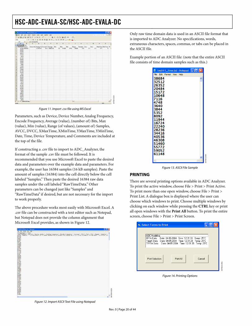
To import raw time domain text data in decimal format:
1. Choose File > Import Data.
2. Click the ASCII File button shown in Figure 9.
3. The window in Figure 10 opens. This window is used to give ADC Analyzer information about how to interpret the text data file. If any of these input parameters are not correct, both the time and FFT data will not be correct.
Data Bits: Select the resolution of the ADC.
Samples: Select the number of samples in the file.
Data Format: Select the format of the ADC output data.
Justification: Normally, the data exported from ADC Analyzer is MSB_Justified. When importing data, be sure to select the proper justification.
Encode Frequency (MHz): Enter the sampling clock rate used.
ASCII Text File to Import: Click the Browse… button to search for the file.
4. Click OK. The time-domain data is graphed in a new window. Right click the graph to open the hidden menu. Select Lock Data from the menu. (See Figure 7.)
5. To perform an FFT on this data, click the FFT button.
0475
0-0-
021
Figure 9. Import Data Dialog Box
0475
0-0-
022
Figure 10. Import ASCII Text File Dialog Box
.csv and ASCII files
The Comma Separated Value or Comma Delimited file format (.csv) is displayed in Figure 11 using Microsoft Excel. The .csv file includes extra parameters, including the raw time domain data.
HSC-ADC-EVALA-SC/HSC-ADC-EVALA-DC
0475
0-0-
023
Rev. 0 | Page 20 of 44
Figure 11. Import .csv file using MS Excel
Parameters, such as Device, Device Number, Analog Frequency, Encode Frequency, Average (value), (number of) Bits, Max (value), Min (value), Range (of values), (amount of) Samples, AVCC, DVCC, XMaxTime, XMinTime, YMaxTime, YMinTime, Date, Time, Device Temperature, and Comments are included at the top of the file.
If constructing a .csv file to import to ADC_Analyzer, the format of the sample .csv file must be followed. It is recommended that you use Microsoft Excel to paste the desired data and parameters over the example data and parameters. For example, the user has 16384 samples (16 kB samples). Paste the amount of samples (16384) into the cell directly below the cell labeled “Samples.” Then paste the desired 16384 raw data samples under the cell labeled “RawTimeData.” Other parameters can be changed just like “Samples” and “RawTimeData” if desired, but are not necessary for the import to work properly.
The above procedure works most easily with Microsoft Excel. A .csv file can be constructed with a text editor such as Notepad, but Notepad does not provide the column alignment that Microsoft Excel provides, as shown in Figure 12.
0475
0-0-
024
Figure 12. Import ASCII Text File using Notepad
Only raw time domain data is used in an ASCII file format that is imported to ADC Analyzer. No specifications, words, extraneous characters, spaces, commas, or tabs can be placed in the ASCII file.
Example portion of an ASCII file: (note that the entire ASCII file consists of time domain samples such as this.)
0475
0-0-
054
Figure 13. ASCII File Sample
PRINTING There are several printing options available in ADC Analyzer. To print the active window, choose File > Print > Print Active. To print more than one open window, choose File > Print > Print List. A dialogue box is displayed where the user can choose which windows to print. Choose multiple windows by clicking on each window while pressing the CTRL key or print all open windows with the Print All button. To print the entire screen, choose File > Print > Print Screen.
0475
0-0-
051
Figure 14. Printing Options
HSC-ADC-EVALA-SC/HSC-ADC-EVALA-DC
Rev. 0 | Page 21 of 44
SAVING FILES There are three ways to save an image in ADC Analyzer. Choose File > Save As > Save Active to save the active window in bitmap or jpeg format. Choose File > Save As > Save List to save each open window as a separate bitmap file. To save the entire screen as a bitmap file, choose File > Save As > Save Screen.
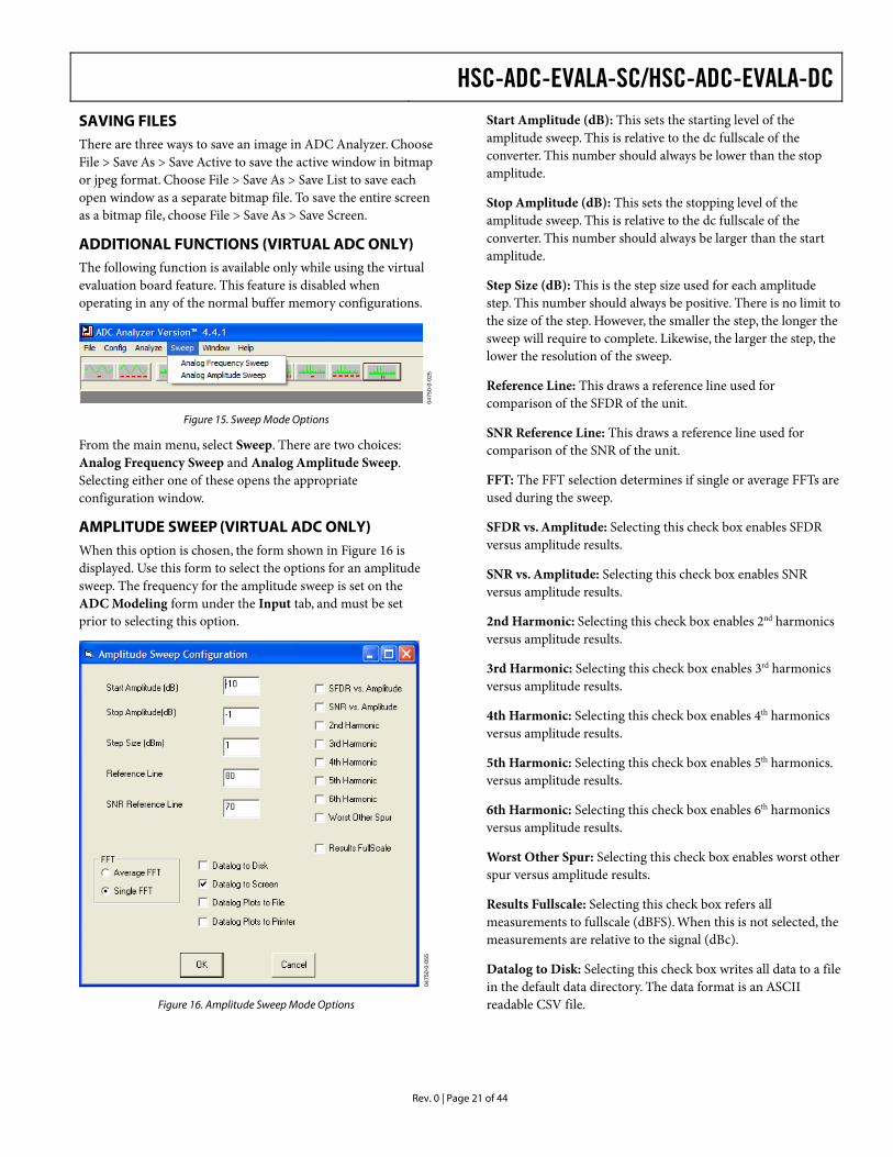
ADDITIONAL FUNCTIONS (VIRTUAL ADC ONLY) The following function is available only while using the virtual evaluation board feature. This feature is disabled when operating in any of the normal buffer memory configurations.
0475
0-0-
025
Figure 15. Sweep Mode Options
From the main menu, select Sweep. There are two choices: Analog Frequency Sweep and Analog Amplitude Sweep. Selecting either one of these opens the appropriate configuration window.
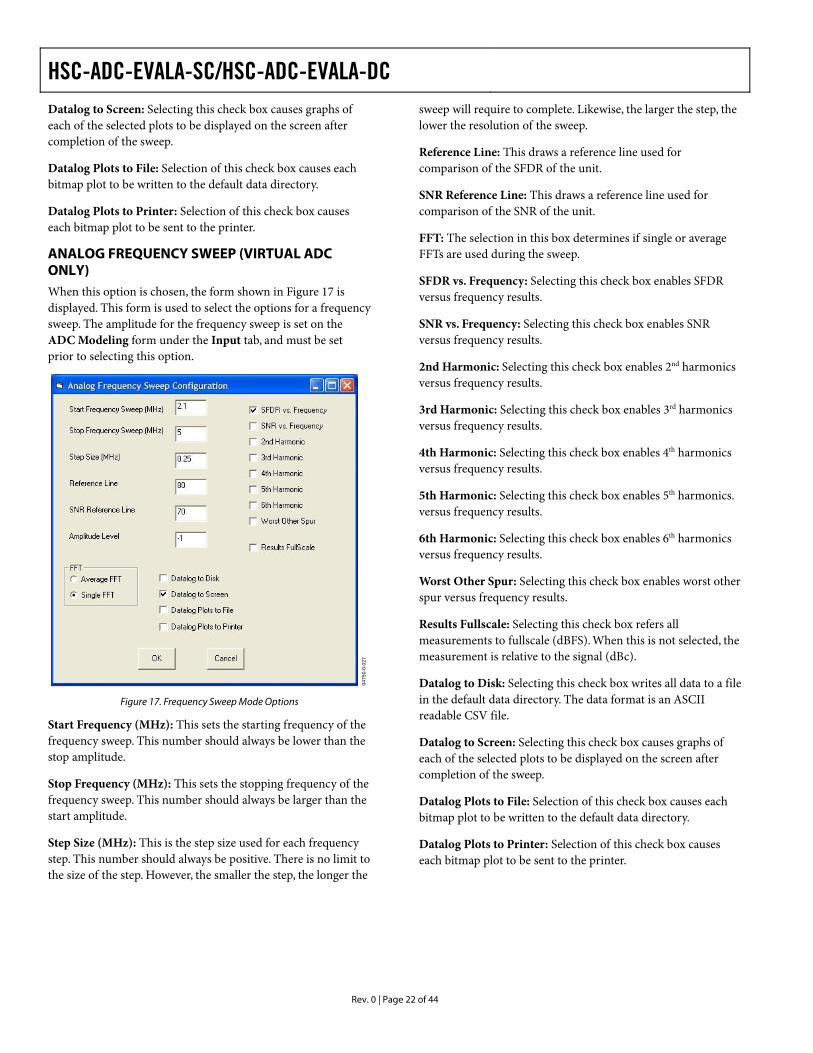
AMPLITUDE SWEEP (VIRTUAL ADC ONLY) When this option is chosen, the form shown in Figure 16 is displayed. Use this form to select the options for an amplitude sweep. The frequency for the amplitude sweep is set on the ADC Modeling form under the Input tab, and must be set prior to selecting this option.
0475
0-0-
055
Figure 16. Amplitude Sweep Mode Options
Start Amplitude (dB): This sets the starting level of the amplitude sweep. This is relative to the dc fullscale of the converter. This number should always be lower than the stop amplitude.
Stop Amplitude (dB): This sets the stopping level of the amplitude sweep. This is relative to the dc fullscale of the converter. This number should always be larger than the start amplitude.
Step Size (dB): This is the step size used for each amplitude step. This number should always be positive. There is no limit to the size of the step. However, the smaller the step, the longer the sweep will require to complete. Likewise, the larger the step, the lower the resolution of the sweep.
Reference Line: This draws a reference line used for comparison of the SFDR of the unit.
SNR Reference Line: This draws a reference line used for comparison of the SNR of the unit.
FFT: The FFT selection determines if single or average FFTs are used during the sweep.
SFDR vs. Amplitude: Selecting this check box enables SFDR versus amplitude results.
SNR vs. Amplitude: Selecting this check box enables SNR versus amplitude results.
2nd Harmonic: Selecting this check box enables 2nd harmonics versus amplitude results.
3rd Harmonic: Selecting this check box enables 3rd harmonics versus amplitude results.
4th Harmonic: Selecting this check box enables 4th harmonics versus amplitude results.
5th Harmonic: Selecting this check box enables 5th harmonics. versus amplitude results.
6th Harmonic: Selecting this check box enables 6th harmonics versus amplitude results.
Worst Other Spur: Selecting this check box enables worst other spur versus amplitude results.
Results Fullscale: Selecting this check box refers all measurements to fullscale (dBFS). When this is not selected, the measurements are relative to the signal (dBc).
Datalog to Disk: Selecting this check box writes all data to a file in the default data directory. The data format is an ASCII readable CSV file.
HSC-ADC-EVALA-SC/HSC-ADC-EVALA-DC
Rev. 0 | Page 22 of 44
Datalog to Screen: Selecting this check box causes graphs of each of the selected plots to be displayed on the screen after completion of the sweep.
sweep will require to complete. Likewise, the larger the step, the lower the resolution of the sweep.
Reference Line: This draws a reference line used for comparison of the SFDR of the unit. Datalog Plots to File: Selection of this check box causes each
bitmap plot to be written to the default data directory. SNR Reference Line: This draws a reference line used for comparison of the SNR of the unit. Datalog Plots to Printer: Selection of this check box causes
each bitmap plot to be sent to the printer. FFT: The selection in this box determines if single or average FFTs are used during the sweep. ANALOG FREQUENCY SWEEP (VIRTUAL ADC
ONLY) SFDR vs. Frequency: Selecting this check box enables SFDR versus frequency results. When this option is chosen, the form shown in Figure 17 is
displayed. This form is used to select the options for a frequency sweep. The amplitude for the frequency sweep is set on the ADC Modeling form under the Input tab, and must be set prior to selecting this option.
SNR vs. Frequency: Selecting this check box enables SNR versus frequency results.
2nd Harmonic: Selecting this check box enables 2nd harmonics versus frequency results.
0475
0-0-
027
3rd Harmonic: Selecting this check box enables 3rd harmonics versus frequency results.
4th Harmonic: Selecting this check box enables 4th harmonics versus frequency results.
5th Harmonic: Selecting this check box enables 5th harmonics. versus frequency results.
6th Harmonic: Selecting this check box enables 6th harmonics versus frequency results.
Worst Other Spur: Selecting this check box enables worst other spur versus frequency results.
Results Fullscale: Selecting this check box refers all measurements to fullscale (dBFS). When this is not selected, the measurement is relative to the signal (dBc).
Datalog to Disk: Selecting this check box writes all data to a file in the default data directory. The data format is an ASCII readable CSV file.
Figure 17. Frequency Sweep Mode Options
Start Frequency (MHz): This sets the starting frequency of the frequency sweep. This number should always be lower than the stop amplitude.
Datalog to Screen: Selecting this check box causes graphs of each of the selected plots to be displayed on the screen after completion of the sweep.
Stop Frequency (MHz): This sets the stopping frequency of the frequency sweep. This number should always be larger than the start amplitude.
Datalog Plots to File: Selection of this check box causes each bitmap plot to be written to the default data directory.
Step Size (MHz): This is the step size used for each frequency step. This number should always be positive. There is no limit to the size of the step. However, the smaller the step, the longer the
Datalog Plots to Printer: Selection of this check box causes each bitmap plot to be sent to the printer.
HSC-ADC-EVALA-SC/HSC-ADC-EVALA-DC
Rev. 0 | Page 23 of 44
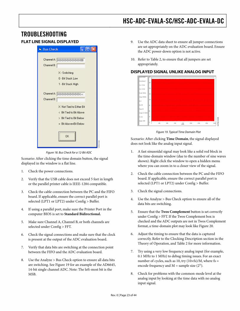
TROUBLESHOOTINGFLAT LINE SIGNAL DISPLAYED
0475
0-0-
028
Figure 18. Bus Check for a 12-Bit ADC
Scenario: After clicking the time domain button, the signal displayed in the window is a flat line.
1. Check the power connections.
2. Verify that the USB cable does not exceed 5 feet in length or the parallel printer cable is IEEE-1284 compatible.
3. Check the cable connection between the PC and the FIFO board. If applicable, ensure the correct parallel port is selected (LPT1 or LPT2) under Config > Buffer.
4. If using a parallel port, make sure the Printer Port in the computer BIOS is set to Standard Bidirectional.
5. Make sure Channel A, Channel B, or both channels are selected under Config > FFT.
6. Check the signal connections and make sure that the clock is present at the output of the ADC evaluation board.
7. Verify that data bits are switching at the connection point between the FIFO and the ADC evaluation board.
8. Use the Analyze > Bus Check option to ensure all data bits are switching. See Figure 19 for an example of the AD6645, 14-bit single channel ADC. Note: The left-most bit is the MSB.
9. Use the ADC data sheet to ensure all jumper connections are set appropriately on the ADC evaluation board. Ensure the ADC power-down option is not active.
10. Refer to Table 2, to ensure that all jumpers are set appropriately.
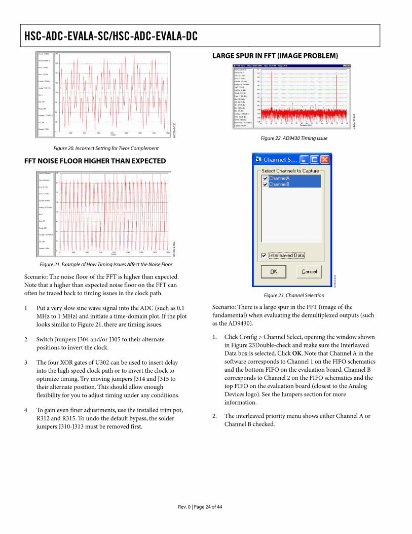
DISPLAYED SIGNAL UNLIKE ANALOG INPUT
0475
0-0-
029
Figure 19. Typical Time Domain Plot
Scenario: After clicking Time Domain, the signal displayed does not look like the analog input signal.
1. A fast sinusoidal signal may look like a solid red block in the time-domain window (due to the number of sine waves shown). Right click the window to open a hidden menu where you can zoom in to a closer view of the signal.
2. Check the cable connection between the PC and the FIFO board. If applicable, ensure the correct parallel port is selected (LPT1 or LPT2) under Config > Buffer.
3. Check the signal connections.
4. Use the Analyze > Bus Check option to ensure all of the data bits are switching.
5. Ensure that the Twos Complement button is set correctly under Config > FFT. If the Twos Complement box is checked and the ADC outputs are not in Twos Complement format, a time-domain plot may look like Figure 20.
6. Adjust the timing to ensure that the data is captured correctly. Refer to the Clocking Description section in the Theory of Operation, and Table 2 for more information.
7. Try using a very low frequency analog input (for example, 0.1 MHz to 1 MHz) to debug timing issues. For an exact number of cycles, such as 10, try (10×fs)/M, where fs = encode frequency and M = sample size (2N).
8. Check for problems with the common-mode level at the analog input by looking at the time data with no analog input signal.
HSC-ADC-EVALA-SC/HSC-ADC-EVALA-DC
Rev. 0 | Page 24 of 44
0475
0-0-
030
Figure 20. Incorrect Setting for Twos Complement
FFT NOISE FLOOR HIGHER THAN EXPECTED
0475
0-0-
031
Figure 21. Example of How Timing Issues Affect the Noise Floor
Scenario: The noise floor of the FFT is higher than expected. Note that a higher than expected noise floor on the FFT can often be traced back to timing issues in the clock path.
1 Put a very slow sine wave signal into the ADC (such as 0.1 MHz to 1 MHz) and initiate a time-domain plot. If the plot looks similar to Figure 21, there are timing issues.
2 Switch Jumpers J304 and/or J305 to their alternate positions to invert the clock.
3 The four XOR gates of U302 can be used to insert delay into the high speed clock path or to invert the clock to optimize timing. Try moving jumpers J314 and J315 to their alternate position. This should allow enough flexibility for you to adjust timing under any conditions.
4 To gain even finer adjustments, use the installed trim pot, R312 and R315. To undo the default bypass, the solder jumpers J310-J313 must be removed first.
LARGE SPUR IN FFT (IMAGE PROBLEM)
0475
0-0-
032
Figure 22. AD9430 Timing Issue
0475
0-0-
033
Figure 23. Channel Selection
Scenario: There is a large spur in the FFT (image of the fundamental) when evaluating the demultiplexed outputs (such as the AD9430).
1. Click Config > Channel Select, opening the window shown in Figure 23Double-check and make sure the Interleaved Data box is selected. Click OK. Note that Channel A in the software corresponds to Channel 1 on the FIFO schematics and the bottom FIFO on the evaluation board. Channel B corresponds to Channel 2 on the FIFO schematics and the top FIFO on the evaluation board (closest to the Analog Devices logo). See the Jumpers section for more information.
2. The interleaved priority menu shows either Channel A or Channel B checked.
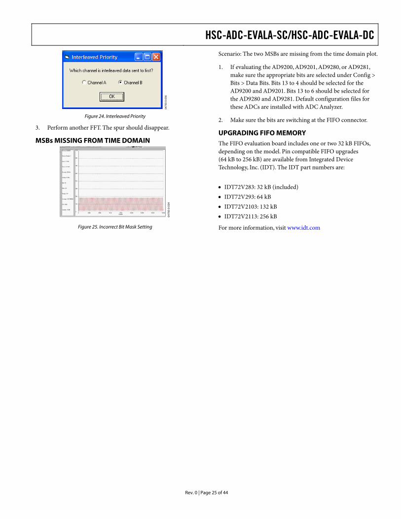
HSC-ADC-EVALA-SC/HSC-ADC-EVALA-DC
Rev. 0 | Page 25 of 44
0475
0-0-
056
Figure 24. Interleaved Priority
3. Perform another FFT. The spur should disappear.
MSBs MISSING FROM TIME DOMAIN
0475
0-0-
034
Figure 25. Incorrect Bit Mask Setting
Scenario: The two MSBs are missing from the time domain plot.
1. If evaluating the AD9200, AD9201, AD9280, or AD9281, make sure the appropriate bits are selected under Config > Bits > Data Bits. Bits 13 to 4 should be selected for the AD9200 and AD9201. Bits 13 to 6 should be selected for the AD9280 and AD9281. Default configuration files for these ADCs are installed with ADC Analyzer.
2. Make sure the bits are switching at the FIFO connector.
UPGRADING FIFO MEMORY The FIFO evaluation board includes one or two 32 kB FIFOs, depending on the model. Pin compatible FIFO upgrades (64 kB to 256 kB) are available from Integrated Device Technology, Inc. (IDT). The IDT part numbers are:
• IDT72V283: 32 kB (included) • IDT72V293: 64 kB • IDT72V2103: 132 kB • IDT72V2113: 256 kB
For more information, visit www.idt.com

HSC-ADC-EVALA-SC/HSC-ADC-EVALA-DC
Rev. 0 | Page 26 of 44
JUMPERSUse the legends below to configure the jumpers. On the FIFO evaluation board, Channel 1 is associated with the bottom IDT FIFO chip, and Channel 2 is associated with the top IDT FIFO chip (closest to the Analog Devices logo).
Table 2. Jumper Legend Position Description In Jumper in place (2-pin header) Out Jumper removed (2-pin header) Position 1 or Position 3 Denotes the position of a 3-pin header. Position 1 is marked on the board.
Table 3 Solder Bridge Legend Position Description In Solder pads should be connected Out Solder pads should not be connected
DEFAULT SETTINGS Table 4 lists the default settings for each model of the FIFO Evaluation Kit. The single channel (SC) model is configured to work with a single channel ADC using the bottom FIFO, U201. The dual channel (DC) model is configured to work with demultiplexed ADCs (such as the AD9430). Dual channel ADC settings are shown in a separate column, as are settings for the opposite (top) FIFO, U101 for a single channel ADC. To align the timing properly, some evaluation boards may require modifications to these settings. Refer to the Clocking Description section in the Theory of Operation section for more information.
Another useful way to configure the jumper settings easily for various configurations is to consult ADC Analyzer under the Help > About HSC_ADC_EVALA, and click Setup Default Jumper Wizard. Then click the configuration setting that applies to the application of interest. A picture of the FIFO board is displayed for that application with a visual of the correct jumper settings already in place.
Table 4. Jumper Configurations
Jumper No.
Single Channel Settings, Default (Bottom)
Demultiplexed Settings
Dual Channel Settings
Single Channel Settings1
(Top) Description J101 Out Out Out Out Not Used J102 Out Out Out Out Not Used J103 In In In In Ground Unused Pins from Input Header J105 In In In In Ground Unused Pins from Input Header J106 Out Out Out Out Not Used J107 Out Out Out Out Not Used J201 Out Out Out Out Not Used J202 Out Out Out Out Not Used J203 In In In In Takes the FF Signal on FIFO1 out of the Circuit J205 In In In In Takes the EF Signal on FIFO1 out of the Circuit J206 Out Out Out Out Not Used J207 Out Out Out Out Not Used J303 In Out Out In OUT for Interleave and Dual/Ties Write Clocks Together J304 Position 3 Position 3 Position 3 Position 3 POS3: Invert Clock out of DS90 J305 Position 3 Position 3 Position 3 Position 3 POS3: Invert Clock out of DS90 J306 Out Out Out Out NO Invert from XOR (U302) J307 Out Out Out Out NO Invert from XOR (U302) J310-13 In In In In All Solder Jumpers are Shorted J314 Position 3 Position 3 Position 3 Position 3 No Timing Delay J315 Position 1 Position 1 Position 1 Position 1 No Timing Delay J401 Position 1 Position 1 Position 1 Position 1 WEN Select

HSC-ADC-EVALA-SC/HSC-ADC-EVALA-DC
Rev. 0 | Page 27 of 44
Jumper No.
Single Channel Settings, Default (Bottom)
Demultiplexed Settings
Dual Channel Settings
Single Channel Settings1
(Top) Description J402 Position 3 Position 3 Position 3 Position 3 WEN Select J403 Position 1 Position 1 Position 1 Position 1 J303 OUT: POS 1 bottom channel, POS 3 Top channel
1 Can only be used with a dual channel FIFO board. This is essentially a single channel, but using the opposite channel (top FIFO) rather than the standard default
(bottom FIFO).

HSC-ADC-EVALA-SC/HSC-ADC-EVALA-DC
Rev. 0 | Page 28 of 44
FIFO SCHEMATICES AND PCB LAYOUT FIFO CONNECTOR
0475
0-0-
037
GNDDRGNDD15 (MSB)D14D13D12D11D10D9D8D7D6D5D4D3D2D1D0 (LSB)FLOAT
403836343230282624222018161412108642
39373533312927252321191715131197531
FLOATFLOATFLOAT
GNDGNDGNDGNDGNDGNDGNDGNDGNDGNDGNDGNDGNDGNDGNDGND
FLOAT
Figure 26. Single-Channel Connector Pin Diagram— Top View (HSC-ADC-EVAL-SC)
0475
0-0-
038
GNDDRGNDD15 (MSB)D14D13D12D11D10D9D8D7D6D5D4D3D2D1D0 (LSB)FLOATGNDDRGNDD15 (MSB)D14D13D12D11D10D9D8D7D6D5D4D3D2D1D0 (LSB)FLOAT
8078767472706866646260585654525048464442403836343230282624222018161412108642
797775737169676563615957555351494745434139373533312927252321191715131197531
FLOATFLOATFLOAT
GNDGNDGNDGNDGNDGNDGNDGNDGNDGNDGNDGNDGNDGNDGNDGND
FLOATFLOATFLOATFLOAT
GNDGNDGNDGNDGNDGNDGNDGNDGNDGNDGNDGNDGNDGNDGNDGND
FLOAT
Figure 27. Dual-Channel Connector Pin Diagram— Top View (HSC-ADC-EVAL-DC)
HSC-ADC-EVALA-SC/HSC-ADC-EVALA-DC
Rev. 0 | Page 29 of 44
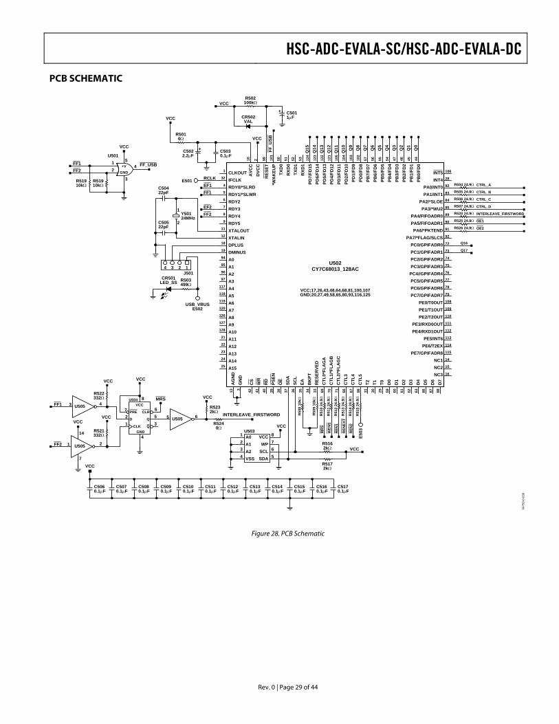
PCB SCHEMATIC
0475
0-0-
039
A0A1
SCLVSSA2
VCCWP
SDA
AG
ND
GN
D
CS
WR
RD
PSEN
OE
SDA
SCL
EA BK
PTR
ESER
VED
IFCLK RES
ET*W
AK
EUP
TXD
0R
XD0
TXD
1R
XD1
D5
D6
D7
CTL
0*FL
AG
AC
TL1/
*FLA
GB
CTL
2/*F
LAG
CC
TL3
CTL
4C
TL5
INT4
T2 T1 T0 D0
D1
D2
D3
D4
NC3NC2NC1
PE7/GPIFADR8PE6/T2EXPE5/INT6
PE4/RXD1OUTPE3/RXD0OUT
PE2/T2OUTPE1/T1OUTPE0/T0OUT
PC7/GPIFADR7PC6/GPIFADR6PC5/GPIFADR5
PC4//GPIFADR4PC3/GPIFADR3PC2/GPIFADR2PC1/GPIFADR1PC0/GPIFADR0
PA7/*FLAG/SLCSPA6/*PKTEND
PA5/FIFOADR1PA4/FIFOADR0
PA3/*WU2PA2/*SLOE
PA1/INT1PA0/INT0
AVC
CD
VCC
PB7/
FD7
PB6/
FD6
PB5/
FD5
PB4/
FD4
PB3/
FD3
PB2/
FD2
PB1/
FD1
PB0/
FD0
PD7/
FD15
PD6/
FD14
PD5/
FD13
PD4/
FD12
PD3/
FD11
PD2/
FD10
PD1/
FD9
PD0/
FD8
A15A14A13A12A11A10A9A8A7A6A5A4A3A2A1A0DMINUSDPLUS
RDY5RDY4RDY3RDY2RDY1/*SLWRRDY0/*SLRD
XTALINXTALOUT
CLKOUT INT5
E503
13 3 42 41 40 39 38 37 36 35 34 33
32
99 101
50 51 52 53
86 87 8869 70 71 66 67 98
28
31 30 29 59 60 61 62 63
16
15
14
115
114
113
112
111
110
109
108
79
78
77
76
75
74
73
72
92
91
90
89
85
84
83
82
10 2 57 56 55 54 47 46 45 44124
123
122
121
105
104
103
102
25
24
23
22
21
128
127
126
120
119
118
117
97
96
95
94
19
18
9
8
7
6
5
4
12
11
1 106
VCC;17,26,43,48,64,68,81,100,107GND;20,27,49,58,65,80,93,116,125
CR501LED_SS
+
1
2
Y50124MHz
Q16
OE1
OE2
INTERLEAVE_FIRSTWORD
CTRL_A
CTRL_B
CTRL_C
CTRL_D
12
56
43
78
U503
14 23J501
CR502VAL
VCC
VCC
FF2EF2
FF1
Q17
Q0
Q1
Q2
Q3
Q4
Q5
Q6
Q7
Q8
Q9
Q10
Q11
Q12
Q13
Q14
Q15FF
_USB
VCC
USB_VBUSE502
EF1
VCC
RCLK
VCC
CY7C68013_128ACU502
R504 24.9Ω
R5010Ω
R502100kΩ
R505 24.9Ω
R506 24.9Ω
R507 24.9Ω
R520 24.9Ω
R525 24.9Ω
R526 24.9Ω
R51
0 24
.9Ω
R50
9 10
kΩ
R50
8 10
kΩ
R51
1 24
.9Ω
R51
2 24
.9Ω
R51
3 24
.9Ω
R51
4 24
.9Ω
R5162kΩ
R5172kΩ
R51
5 24
.9Ω
MR
S
WEN
S
REN
1
REN
EXT
REN
2
R503499Ω
E501C50422pF
C50522pF
C5030.1µF
C5022.2µF
C5011µF
+
VCC
C5060.1µF
C5150.1µF
C5140.1µF
C5130.1µF
C5120.1µF
C5110.1µF
C5100.1µF
C5090.1µF
C5080.1µF
C5070.1µF
C5160.1µF
C5170.1µF
Q
D
CLK
Q
VCC
GND
PRE CLR
VCC
21
5
8
4
7 6
3
U504 MRS
VCC
3 4U505
1 2
14
7
U505FF2
5
VCC
VCC
FF1
R522332Ω
R521332Ω
6U505INTERLEAVE_FIRSTWORD
VCC
R5240Ω
R5232kΩ
R51910kΩ
R51910kΩ
12
3
45
+VGND
FF_USB
VCC
U501
FF1FF2
Figure 28. PCB Schematic
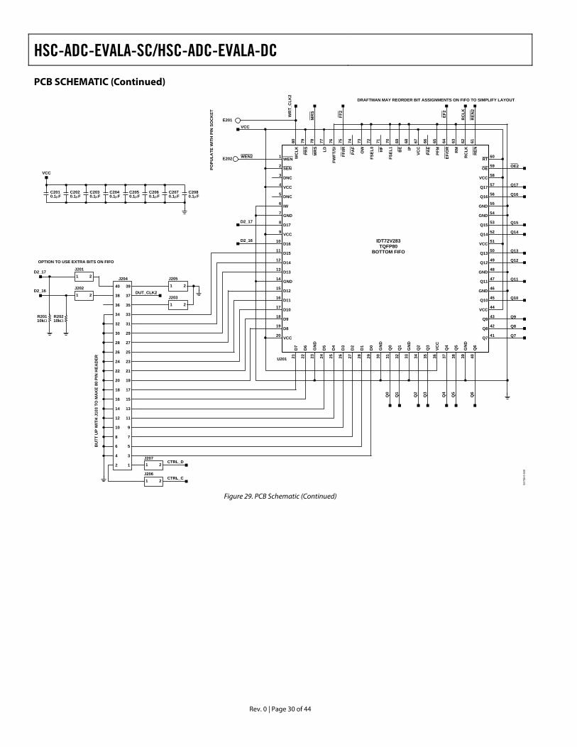
HSC-ADC-EVALA-SC/HSC-ADC-EVALA-DC
Rev. 0 | Page 30 of 44
PCB SCHEMATIC (Continued)
0475
0-0-
040
FF/IRLD
FWFT
/SI
PAF
OW
FSEL
0
HF
FSEL
1
BE IP
PAE
PFM
EF/O
R
RM
RC
LK
REN
Q7
Q8
Q9
Q10
Q11
Q12
Q13
Q14
Q15
Q16
Q17
OE
RT
D5
D4
D3
D2
D1
D0
Q0
Q1
Q2
Q3
Q4
Q5
Q6
D6
D7
D8
D9
D10
D11
D12
D13
D14
D15
D16
D17
IW
SEN
WEN
PRS
WC
LK
MR
S
DNC
VCC
DNC
GND
VCC
GND
VCC
VCC
GND
GND
VCC
GND
GND
VCC
VCC
GN
D
GN
D
GN
D
VCC
GN
D
14
20
23
3
30 33 36 39
4
44
46
48
5
51
54
55
58
67
7
9
2928
17
16
15
13
12
11
10
8
272625242221
19
18
6475 72 7076 68
6
77 73 65
31 32
45
47
49
50
52
53
56
57
34 35 37 38 40
41
42
43
626380 697178
59
667479 61
60
2
1
U201
IDT72V283TQFP80
BOTTOM FIFO
Q9
2
25
39
37
35
33
31
29
27
23
21
19
17
15
13
11
9
7
5
3
1
40
38
36
34
32
30
28
26
24
22
20
18
16
14
12
10
8
6
4
J20421J201
1 2J203
21J205
1 2J206
21J207
1 2J202
R20110kΩ
E202
E201
DUT_CLK2
CTRL_D
CTRL_C
OE2
REN
2
EF2
FF2
WEN2
D2_16
D2_17
VCC
RC
LK
Q0
Q1
Q2
Q3
Q4
Q5
Q6
Q7
Q8
Q10
Q11
Q13
Q14
Q15
Q16
Q17
MR
S
WR
T_C
LK2
Q12
D2_17
D2_16
DRAFTMAN MAY REORDER BIT ASSIGNMENTS ON FIFO TO SIMPLIFY LAYOUT
POPU
LATE
WIT
H P
IN S
OC
KET
R20210kΩ
OPTION TO USE EXTRA BITS ON FIFO
BU
TT U
P W
ITH
J10
3 TO
MA
KE
80 P
IN H
EAD
ER
VCC
C2010.1µF
C2020.1µF
C2030.1µF
C2040.1µF
C2050.1µF
C2060.1µF
C2070.1µF
C2080.1µF
Figure 29. PCB Schematic (Continued)
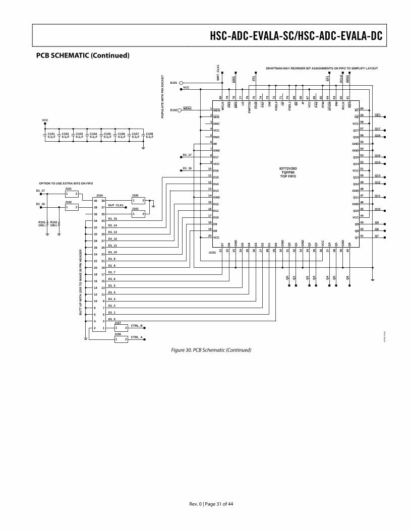
HSC-ADC-EVALA-SC/HSC-ADC-EVALA-DC
Rev. 0 | Page 31 of 44
PCB SCHEMATIC (Continued)
0475
0-0-
041
FF/IRLD
FWFT
/SI
PAF
OW
FSEL
0
HF
FSEL
1
BE IP
PAE
PFM
EF/O
R
RM
RC
LK
REN
Q7
Q8
Q9
Q10
Q11
Q12
Q13
Q14
Q15
Q16
Q17
OE
RT
D5
D4
D3
D2
D1
D0
Q0
Q1
Q2
Q3
Q4
Q5
Q6
D6
D7
D8
D9
D10
D11
D12
D13
D14
D15
D16
D17
IW
SEN
WEN
PRS
WC
LK
MR
S
DNC
VCC
DNC
GND
VCC
GND
VCC
VCC
GND
GND
VCC
GND
GND
VCC
VCC
GN
D
GN
D
GN
D
VCC
GN
D
14
2023
3
30 33 36 39
4
44
46
48
5
51
54
55
58
67
7
9
2928
17
16
15
13
12
11
10
8
272625242221
19
18
6475 72 7076 68
6
77 73 65
31 32
45
47
49
50
52
53
56
57
34 35 37 38 40
41
42
43
626380 697178
59
667479 61
60
2
1
U101
IDT72V283TQFP80
TOP FIFO
Q9
2
25
39
37
35
33
31
29
27
23
21
19
17
15
13
11
9
7
5
3
1
40
38
36
34
32
30
28
26
24
22
20
18
16
14
12
10
8
6
4
J10421J101
1 2J103
D1_15
21J105
1 2J106
21J107
1 2J102
R10110kΩ
E102
D1_6
E101
D1_0
D1_1
D1_2
D1_3
D1_4
D1_5
D1_7
D1_8
D1_9
D1_10
D1_11
D1_12
D1_13
D1_14
DUT_CLK1
CTRL_B
CTRL_A
OE1
REN
1
EF1
FF1
WEN1
D1_16
D1_17
VCC
RC
LK
Q0
Q1
Q2
Q3
Q4
Q5
Q6
Q7
Q8
Q10
Q11
Q13
Q14
Q15
Q16
Q17
MR
S
WR
T_C
LK1
Q12
D1_17
D1_16
DRAFTMAN MAY REORDER BIT ASSIGNMENTS ON FIFO TO SIMPLIFY LAYOUT
POPU
LATE
WIT
H P
IN S
OC
KET
R10210kΩ
OPTION TO USE EXTRA BITS ON FIFO
BU
TT U
P W
ITH
J20
3 TO
MA
KE
80 P
IN H
EAD
ER
VCC
C1010.1µF
C1020.1µF
C1030.1µF
C1040.1µF
C1050.1µF
C1060.1µF
C1070.1µF
C1080.1µF
Figure 30. PCB Schematic (Continued)

HSC-ADC-EVALA-SC/HSC-ADC-EVALA-DC
Rev. 0 | Page 32 of 44
PCB SCHEMATIC (Continued)
0475
0-0-
042
TOP FIFO BOTTOM FIFO
1
10
11 12
13 14
15 16
17 18
19
2
20
3 4
5 6
7 8
9
J308
HEADER 20
E304E303
WENS
WRT_CLK2WRT_CLK1
RCLK
EF2
FF2FF1
EF1
OE1 OE2
REN2REN1
MRS
VCC
12
J309
CON_2P_5MM
VCC
+ C30710µF
+ C30910µF
C3080.1µF
RIN1+2
GND12U301
EN
6
VCC
13
ROUT214
ROUT115
ROUT311
ROUT410
RIN1–1
RIN2+3
RIN2–4
RIN3+6
RIN3–5
RIN4+7
RIN4–8
DS90LV048A
C3050.1µF
VCC
1
3
J304
J305
3
1
C3060.1µF
2 1J306 R309
1kΩ
2 1J307 R310
1kΩ
12
3U302
74VCX86
109
8U302
74VCX86
VCC
1213
11U302
74VCX86 HEA
DER
J3 3 J315
1
WRT_CLK2
54
6U302
74VCX86 HEA
DER
J3 3 J314
1
WRT_CLK1
E305
E306
EN
9
J312
JMP0508
J313
JMP0508R316331Ω
R315
R314331Ω
C3110.1µF
VCC
J310
JMP0508
J311
JMP0508R313331Ω
R312
R311331Ω
C3100.1µF
VCC
PLA
CE
JUM
PER
S B
ETW
EEN
PA
DS
ON
TO
P SI
DE
J303
HEADER J4
1
3
2
4
R306DNP
R305DNP
R307331Ω
R308331Ω
EXT_CLK2
VCC VCC
C3040.1µF
J302
R302DNP
R301DNP
R303331Ω
R304331Ω
EXT_CLK1
VCC VCC
C3010.1µF
J301
TOP FIFODUT_CLK1
C3020.1µF
BOTTOM FIFODUT_CLK2
C3030.1µF
E301E302
POPULATE WITHPIN SOCKET
Figure 31. PCB Schematic (Continued)
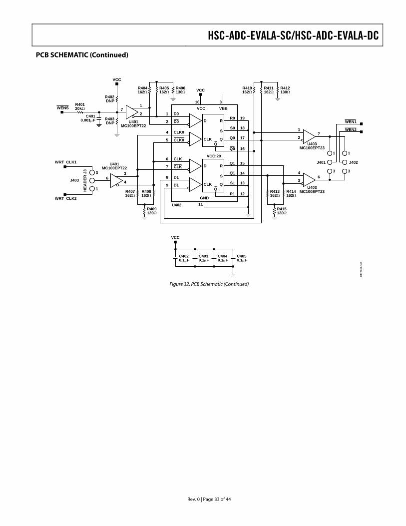
HSC-ADC-EVALA-SC/HSC-ADC-EVALA-DC
Rev. 0 | Page 33 of 44
PCB SCHEMATIC (Continued)
0475
0-0-
043
1 D0
2 D0
4 CLK0
5 CLK0
D
CLK
R
S
R0 19
S0 18
Q0 17
Q0 16
6 CLK
7 CLK D
CLK
R
S
Q1 15
Q1 14
S1 13
R1 12
VCC;20
GND11
VCC10
VBB3
U402
WEN1
WEN2
1 1
4
36
U403MC100EPT23
72
1
U401MC100EPT22
3 3
1
27
U403MC100EPT23
J402J401
R413162Ω
R414162Ω
R415130Ω
R407162Ω
R408162Ω
R409130Ω
8 D1
9 D1
R410162Ω
R411162Ω
R412130Ω
R404162Ω
R405162Ω
R406130Ω
R403DNP
R402DNP
R40120kΩ
VCC
VCC
C4010.001µF
WENS
46J403
WRT_CLK1
WRT_CLK2
3
U401MC100EPT22
HEA
DER
J3 3
1
VCC
C4020.1µF
C4030.1µF
C4040.1µF
C4050.1µF
Figure 32. PCB Schematic (Continued)

HSC-ADC-EVALA-SC/HSC-ADC-EVALA-DC
Rev. 0 | Page 34 of 44
PCB SCHEMATIC (Continued)
0475
0-0-
044
1
10
11
12
13
14
15
16
2
3
4
5
6
7
8 9
R602
DC15
DC14
DC13
DC12
DC10
DC9
DC8
DC11D1_11
D1_8
D1_9
D1_10
D1_12
D1_13
D1_14
D1_15
D1_7
D1_6
D1_5
D1_4
D1_2
D1_1
D1_0
D1_3 DC3
DC0
DC1
DC2
DC4
DC5
DC6
DC7
98
7
6
5
4
3
2
16
15
14
13
12
11
10
1
R601
DC16D1_16
R6030Ω
DC17D1_17R6040Ω
74LCX574
CLOCK
D0
D1
D2
D3
D4
D6
D7
GND
Q0
Q1
Q2
Q3
Q4
Q5
Q6
Q7
VCCOUT_EN
D57
1 20
12
13
14
15
16
17
18
19
10
9
8
6
5
4
3
2
11
U601
98
7
6
5
4
3
2
16
15
14
13
12
11
10
1
RZ605
Q4
Q3
Q0
Q1
Q2
Q5
Q6
Q7
VCC
QL0
QL1
QL2
QL3
QL4
QL5
QL6
QL7
RENEXT
RCLK
VCC
C6010.1µF
QL1
QL2
QL5
QL6
QL7
QL4
QL0
9
8
7
68
67
66
65
64
63
62
61
60
6
59
58
57
56
55
54
53
52
51
50
5
49
48
47
46
45
44
43
42
41
40
4
39
38
37
36
35
34
33
32
31
30
3
29
28
27
26
25
24
23
22
21
20
2
19
18
17
16
15
14
13
12
11
10
1J601
DC9
DC1
EF1
DC12
DC14
DC15
DC4
DC5
QL3
WRT_CLK1
FF1WEN1
MRS
RCLK
REN1
DC10
DC11
DC7
DC8
DC2
DC3
DC0
DC6
DC13
DC16
DC17
Figure 33. PCB Schematic (Continued)
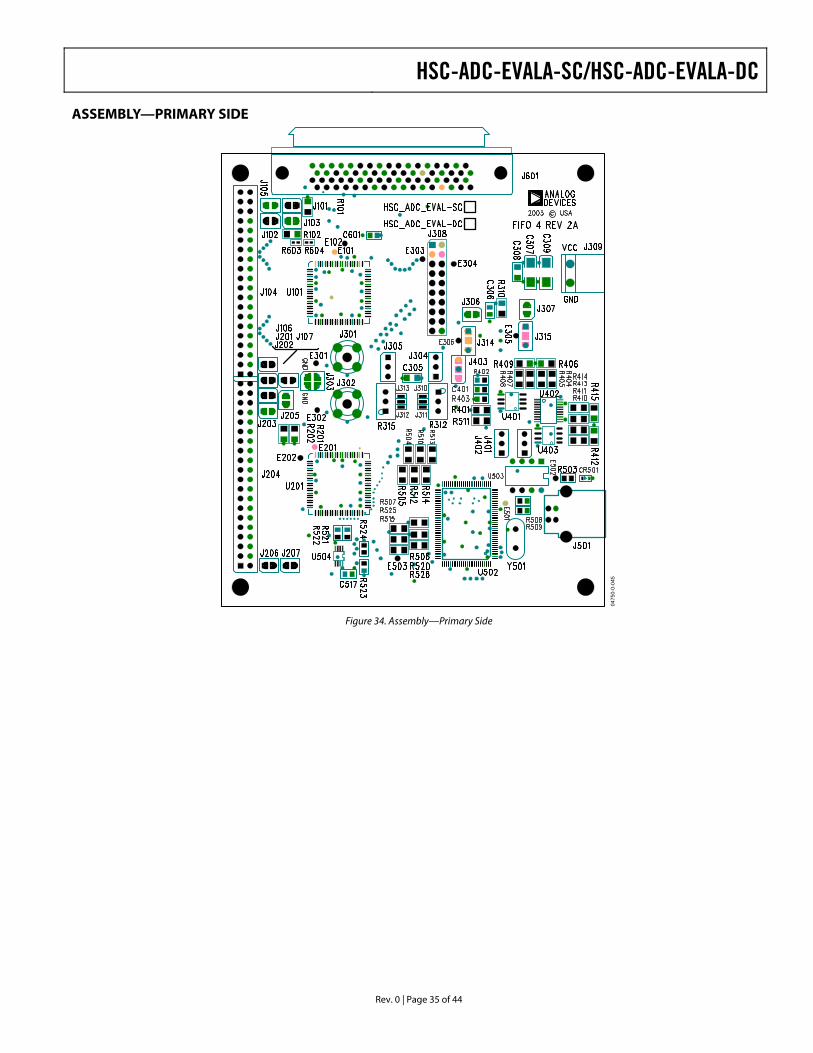
HSC-ADC-EVALA-SC/HSC-ADC-EVALA-DC
Rev. 0 | Page 35 of 44
ASSEMBLY—PRIMARY SIDE
0475
0-0-
045
Figure 34. Assembly—Primary Side
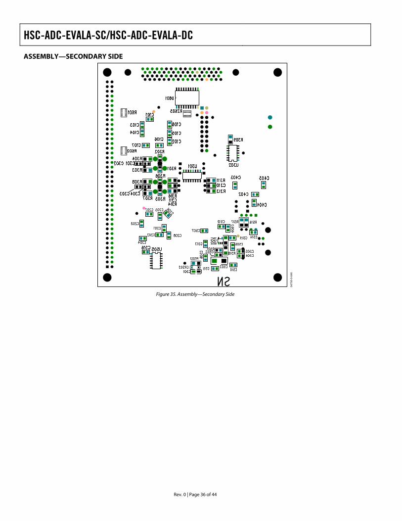
HSC-ADC-EVALA-SC/HSC-ADC-EVALA-DC
Rev. 0 | Page 36 of 44
ASSEMBLY—SECONDARY SIDE
0475
0-0-
046
Figure 35. Assembly—Secondary Side
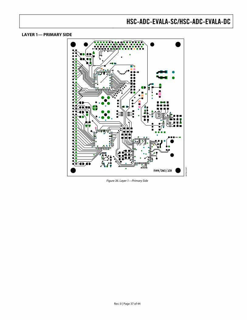
HSC-ADC-EVALA-SC/HSC-ADC-EVALA-DC
Rev. 0 | Page 37 of 44
LAYER 1— PRIMARY SIDE
0475
0-0-
047
Figure 36. Layer 1—Primary Side
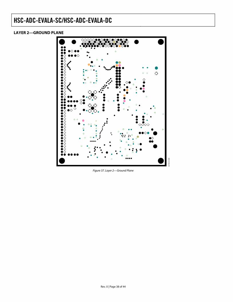
HSC-ADC-EVALA-SC/HSC-ADC-EVALA-DC
Rev. 0 | Page 38 of 44
LAYER 2—GROUND PLANE
0475
0-0-
048
Figure 37. Layer 2—Ground Plane
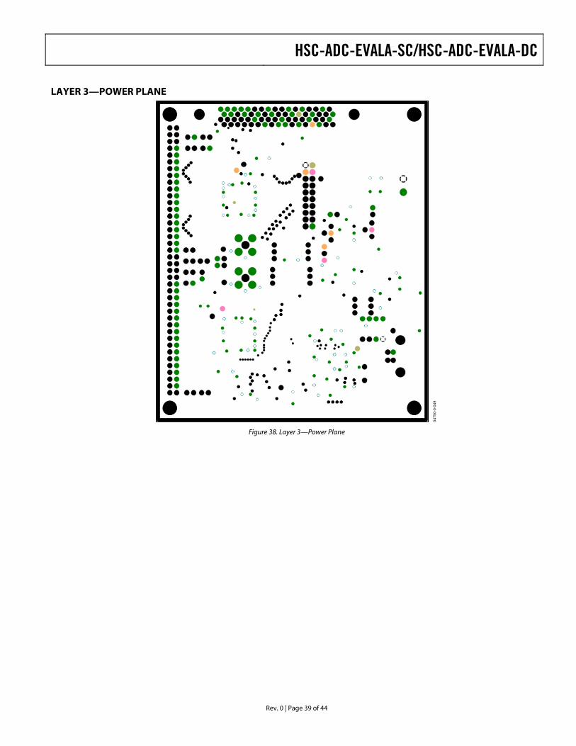
HSC-ADC-EVALA-SC/HSC-ADC-EVALA-DC
Rev. 0 | Page 39 of 44
LAYER 3—POWER PLANE
0475
0-0-
049
Figure 38. Layer 3—Power Plane
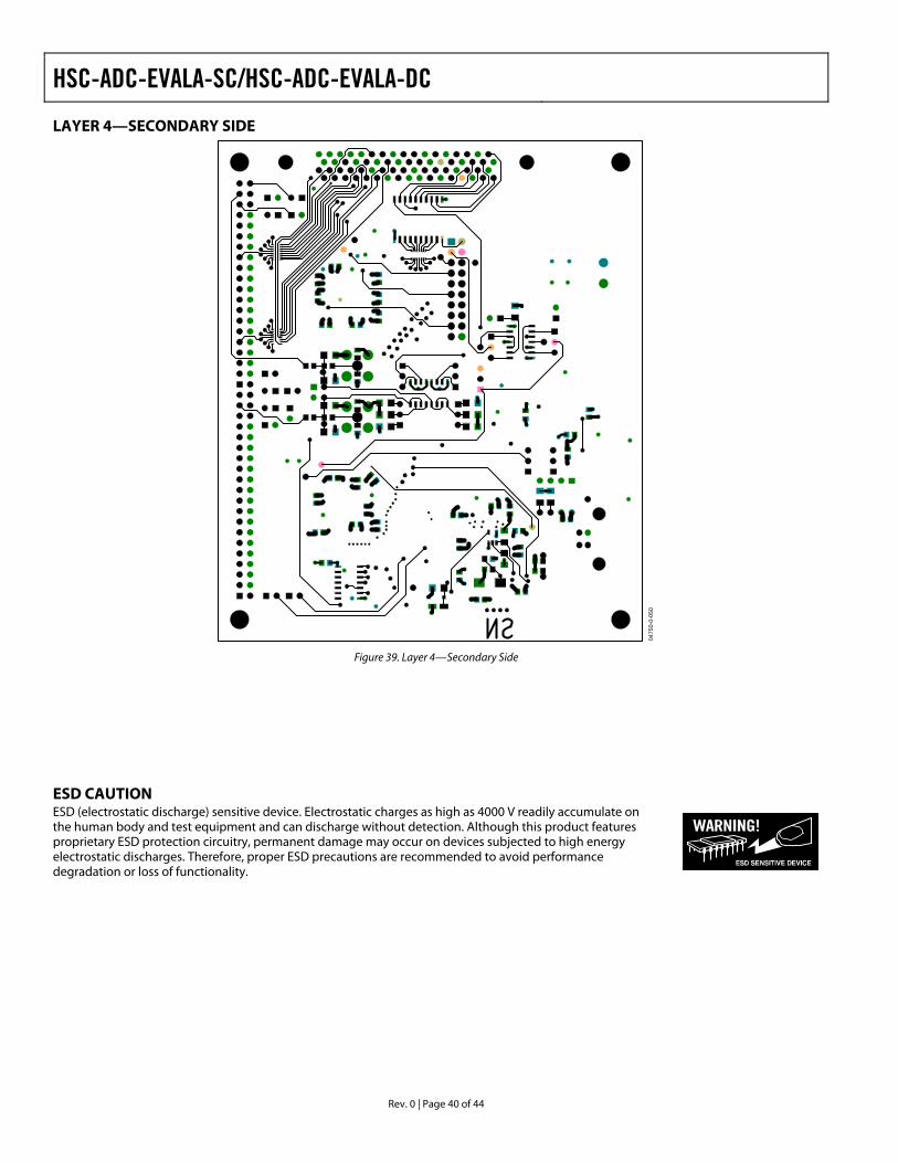
HSC-ADC-EVALA-SC/HSC-ADC-EVALA-DC
Rev. 0 | Page 40 of 44
LAYER 4—SECONDARY SIDE
0475
0-0-
050
Figure 39. Layer 4—Secondary Side
ESD CAUTION ESD (electrostatic discharge) sensitive device. Electrostatic charges as high as 4000 V readily accumulate on the human body and test equipment and can discharge without detection. Although this product features proprietary ESD protection circuitry, permanent damage may occur on devices subjected to high energy electrostatic discharges. Therefore, proper ESD precautions are recommended to avoid performance degradation or loss of functionality.
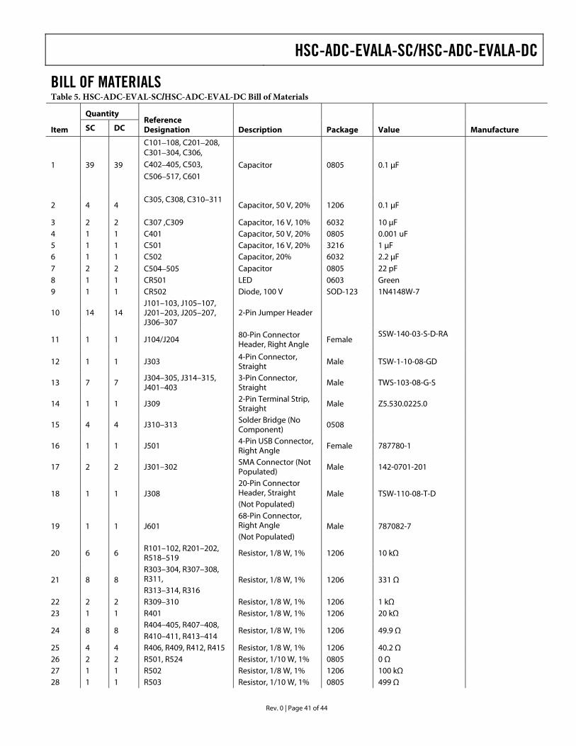
HSC-ADC-EVALA-SC/HSC-ADC-EVALA-DC
Rev. 0 | Page 41 of 44
BILL OF MATERIALS Table 5. HSC-ADC-EVAL-SC/HSC-ADC-EVAL-DC Bill of Materials
Quantity
Item SC DC Reference Designation Description Package Value Manufacture
1 39 39
C101–108, C201–208, C301–304, C306, C402–405, C503, C506–517, C601
Capacitor 0805 0.1 µF
2 4 4 C305, C308, C310–311
Capacitor, 50 V, 20% 1206 0.1 µF
3 2 2 C307 ,C309 Capacitor, 16 V, 10% 6032 10 µF 4 1 1 C401 Capacitor, 50 V, 20% 0805 0.001 uF 5 1 1 C501 Capacitor, 16 V, 20% 3216 1 µF 6 1 1 C502 Capacitor, 20% 6032 2.2 µF 7 2 2 C504–505 Capacitor 0805 22 pF 8 1 1 CR501 LED 0603 Green 9 1 1 CR502 Diode, 100 V SOD-123 1N4148W-7
10 14 14 J101–103, J105–107, J201–203, J205–207, J306–307
2-Pin Jumper Header
11 1 1 J104/J204 80-Pin Connector Header, Right Angle
Female SSW-140-03-S-D-RA
12 1 1 J303 4-Pin Connector, Straight
Male TSW-1-10-08-GD
13 7 7 J304–305, J314–315, J401–403
3-Pin Connector, Straight
Male TWS-103-08-G-S
14 1 1 J309 2-Pin Terminal Strip, Straight
Male Z5.530.0225.0
15 4 4 J310–313 Solder Bridge (No Component)
0508
16 1 1 J501 4-Pin USB Connector, Right Angle
Female 787780-1
17 2 2 J301–302 SMA Connector (Not Populated)
Male 142-0701-201
18 1 1 J308 20-Pin Connector Header, Straight (Not Populated)
Male TSW-110-08-T-D
19 1 1 J601 68-Pin Connector, Right Angle (Not Populated)
Male 787082-7
20 6 6 R101–102, R201–202, R518–519
Resistor, 1/8 W, 1% 1206 10 kΩ
21 8 8 R303–304, R307–308, R311, R313–314, R316
Resistor, 1/8 W, 1% 1206 331 Ω
22 2 2 R309–310 Resistor, 1/8 W, 1% 1206 1 kΩ 23 1 1 R401 Resistor, 1/8 W, 1% 1206 20 kΩ
24 8 8 R404–405, R407–408, R410–411, R413–414
Resistor, 1/8 W, 1% 1206 49.9 Ω
25 4 4 R406, R409, R412, R415 Resistor, 1/8 W, 1% 1206 40.2 Ω 26 2 2 R501, R524 Resistor, 1/10 W, 1% 0805 0 Ω 27 1 1 R502 Resistor, 1/8 W, 1% 1206 100 kΩ 28 1 1 R503 Resistor, 1/10 W, 1% 0805 499 Ω
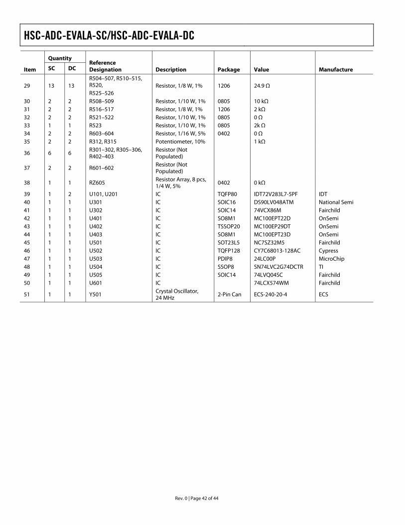
HSC-ADC-EVALA-SC/HSC-ADC-EVALA-DC
Rev. 0 | Page 42 of 44
Quantity
Item SC DC Reference Designation Description Package Value Manufacture
29 13 13 R504–507, R510–515, R520, R525–526
Resistor, 1/8 W, 1% 1206 24.9 Ω
30 2 2 R508–509 Resistor, 1/10 W, 1% 0805 10 kΩ 31 2 2 R516–517 Resistor, 1/8 W, 1% 1206 2 kΩ 32 2 2 R521–522 Resistor, 1/10 W, 1% 0805 0 Ω 33 1 1 R523 Resistor, 1/10 W, 1% 0805 2k Ω 34 2 2 R603–604 Resistor, 1/16 W, 5% 0402 0 Ω 35 2 2 R312, R315 Potentiometer, 10% 1 kΩ
36 6 6 R301–302, R305–306, R402–403
Resistor (Not Populated)
37 2 2 R601–602 Resistor (Not Populated)
38 1 1 RZ605 Resistor Array, 8 pcs, 1/4 W, 5%
0402 0 kΩ
39 1 2 U101, U201 IC TQFP80 IDT72V283L7-5PF IDT 40 1 1 U301 IC SOIC16 DS90LV048ATM National Semi 41 1 1 U302 IC SOIC14 74VCX86M Fairchild 42 1 1 U401 IC SO8M1 MC100EPT22D OnSemi 43 1 1 U402 IC TSSOP20 MC100EP29DT OnSemi 44 1 1 U403 IC SO8M1 MC100EPT23D OnSemi 45 1 1 U501 IC SOT23L5 NC7SZ32M5 Fairchild 46 1 1 U502 IC TQFP128 CY7C68013-128AC Cypress 47 1 1 U503 IC PDIP8 24LC00P MicroChip 48 1 1 U504 IC SSOP8 SN74LVC2G74DCTR TI 49 1 1 U505 IC SOIC14 74LVQ04SC Fairchild 50 1 1 U601 IC 74LCX574WM Fairchild
51 1 1 Y501 Crystal Oscillator, 24 MHz
2-Pin Can ECS-240-20-4 ECS

HSC-ADC-EVALA-SC/HSC-ADC-EVALA-DC
Rev. 0 | Page 43 of 44
APPENDIX: SAMPLING AND FFT FUNDAMENTALSCOHERENT SAMPLING In a coherent system, the analog and clock sources must be synchronized, and the analog and clock input frequencies must be selected such that given 2N (N is an integer number) samples, there is an integer number of whole sine wave cycles. The number of cycles should ideally be a prime number. Selecting a prime number ensures that the same converter codes are not repeated over and over, therefore exercising as many converter codes as possible. Although a crystal oscillator can be used as an clock source in this technique, two synchronized signal synthesizers are generally preferred because special hardware may be required to ensure the crystal oscillator is synchronized with the analog source. The following equation can be used to mathematically calculate the correct analog and clock frequencies for a coherent system:
McM
fsfin
=
where:
fin = Analog Input Frequency
fs = Sampling Clock (encode) Frequency
M = Sample Size (2N)
Mc = Number of Cycles of Sine Wave
If the requirements of the coherent system defined above are not met, the discrete time samples will appear discontinuous at the end of the captured samples and the results will be invalid.
WINDOWING FUNCTIONS It is sometimes desirable to use a windowing function instead of coherent sampling to reduce the restrictions on the analog and encode sources. Two popular windowing functions are the Blackman Harris 4-Term and the Hanning window. With windowing, the time-domain samples are multiplied by the appropriate weighting function that weights the time-domain data such that the discontinuities at the end of the captured samples have less significance. The weighting function for a Blackman Harris 4-Term window is:
⎜⎜⎝
⎛⎟⎟⎠
⎞×π×−⎟⎟
⎠
⎞⎜⎜⎝
⎛ ×π×+⎜⎜
⎝
⎛⎟⎟⎠
⎞×π×−=
Mn
aM
na
Mn
aaWn32
cos322
cos22
cos10
where:
a0 = 0.35875
a1 = 0.48829
a2 = 0.14128
a3 = 0.01168
M = Sample Size (2N)
n = Indexed Sample Number
The weighting function for a Hanning window is:
⎟⎟⎠
⎞⎜⎝⎛ ×
×−=M
n2πcos0.50.5Wn
where:
M = Sample Size(2N)
n = Indexed Sample Number
FFT CALCULATIONS Whether a system is coherent or a windowing function has been applied, the resulting data will be processed via a discrete fourier analysis that translates the discrete time-domain samples into the frequency domain. Because in practice processing the data quickly is desired, a Fast Fourier Transform (FFT) is used, which is simply an algorithm that reduces the required mathematical calculations. There are many FFT algorithms available but the most popular is the radix 2 algorithm. Regardless of the algorithm, for each time-domain sample a complex conjugate pair (r ± jx) will be generated from the FFT. For example, if the time-domain sample size is 16,384, the resulting FFT array will contain 16,384 complex samples. To generate a frequency domain plot from this data, the magnitude of each complex sample must be calculated. The magnitude can be computed using the following equation:
22 ImReMagnitude +=
If the input data to the FFT is complex, the FFT will contain 16,384 magnitudes representing frequencies between plus and minus fs/2. Although complex ADCs are not available, it is very common to use two ADCs to synchronously sample the I and Q data streams from a quadrature demodulator. If the data input to the FFT is real, representing the data from a single ADC, the last 8192 samples represent a mirror image of the first 8192 samples. Because this is an exact mirror image, the last 8192 samples can be ignored.
With the data set processed, there are two ways to evaluate the ADC performance, graphically and computationally. To plot the data in a meaningful way, the magnitude data must be converted to decibels (dB). This can be done with the formula:
⎜⎜⎝
⎛⎟⎠⎞×=
FullScaleMagnitude
10log10dB
where Magnitude is the individual array elements computed above, and FullScale is the FullScale magnitude. It is important to note that the computation for dB assumes the square root
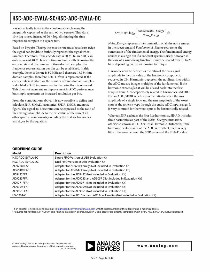
HSC-ADC-EVALA-SC/HSC-ADC-EVALA-DC
Rev. 0 | Page 44 of 44
was not actually taken in the equation above, leaving the magnitude expressed as the sum of two squares. Therefore 10 × log is used instead of 20 × log, eliminating the time required to compute the square root.
dBgyNoise_Ener
l_EnergyFundamentaSNR ⎜
⎜⎝
⎛⎟⎟⎠
⎞×= 10log20
Noise_Energy represents the summation of all the noise energy in the spectrum, and Fundamental_Energy represents the summation of the fundamental energy. The fundamental energy resides in a single bin if a coherent system is used; however, in the case of a windowing function, it may be spread over 10 to 25 bins, depending on the windowing technique.
Based on Nyquist Theory, the encode rate must be at least twice the signal bandwidth to faithfully represent the signal when sampled. Therefore, if the encode rate is 80 MHz, an ADC can only represent 40 MHz of continuous bandwidth. Knowing the encode rate and the number of time-domain samples, the frequency representation per bin can be established. In this example, the encode rate is 80 MHz and there are 16,384 time-domain samples; therefore, 4880 Hz/bin is represented. If the encode rate is doubled or the number of time-domain samples is doubled, a 3 dB improvement in the noise floor is observed. This does not represent an improvement in ADC performance, but simply represents an increased resolution per bin.
Harmonics can be defined as the ratio of the rms signal amplitude to the rms value of the harmonic component, reported in dBc. Harmonics represent the nonlinearities within the ADC and are integer multiples of the fundamental. If the harmonic exceeds fs/2, it will be aliased back into the first Nyquist zone. A concept closely related to harmonics is SFDR. For an ADC, SFDR is defined as the ratio between the rms amplitude of a single tone and the rms amplitude of the worst spur as the tone is swept through the entire ADC input range. It is very common for the worst spur to be harmonically related.
From the computations above, it is now possible to define and calculate SNR, SINAD, harmonics, SFDR, ENOB, and noise figure. The signal-to-noise ratio can be expressed as the ratio of the rms signal amplitude to the rms value of the sum of all other spectral components, excluding the first six harmonics and dc, or by the equation:
Whereas SNR excludes the first five harmonics, SINAD includes these harmonics as part of the Noise_Energy summation, otherwise known as THD or Total Harmonic Distortion. If the harmonic performance of the ADC is excellent, there is very little difference between the SNR value and the SINAD value.
ORDERING GUIDE Model Description HSC-ADC-EVALA-SC Single FIFO Version of USB Evaluation Kit HSC-ADC-EVALA-DC Dual FIFO Version of USB Evaluation Kit AD922XFFA1 Adapter for AD922x Family (Not included in Evaluation Kit) AD664XFFA1, 2 Adapter for AD664x Family (Not included in Evaluation Kit) AD9432FFA1 Adapter for the AD9432 (Not included in Evaluation Kit) AD9283FFA1 Adapter for the AD9283 and AD9057 (Not included in Evauation Kit) AD9071FFA1 Adapter for the AD9071 (Not included in Evaluation Kit) AD9059FFA1 Adapter for the AD9059 (Not included in Evaluation Kit) AD9051FFA1 Adapter for the AD9051 (Not included in Evaluation Kit) LG-0204A1 Adapter for the AD10xxx and AD13xxx Families (Not included in Evaluation Kit)
1 If an adapter is needed, send an email to [email protected] with the part number of the adapter and a mailing address. 2 Required for Revision C of AD6644 and AD6645 evaluation boards. Revision D and greater are directly compatible with e HSC-ADC-EVALA-SC evaluation board
© 2004 Analog Devices, Inc. All rights reserved. Trademarks and registered trademarks are the property of their respective owners. C04750-0-5/04(0)