hkpca journal no. 13 · hkpca journal no. 13 ... blind-ended vias consisting of a diameter of less...
TRANSCRIPT

HKPCA Journal No. 13
1 / 11
Electroplating Microvias with Improved Plating Distribution
Richard Retallick, Donald DeSalvo, Ronald Blake MacDermid Incorporated, Waterbury, Connecticut USA
Abstract This paper explores the capability to electroplate copper into high aspect ratio microvias. Prior work directed toward processing microvias indicated that as aspect ratios approached 1:1 and absolute depths of 100 microns (4 mils), insufficient plating distribution was observed. The current study of microvia plating performance compares both traditional and periodic pulse reverse copper electroplating as a function of increasing aspect ratios. The results show a manufacturing process incorporating a periodic pulse reverse plating system gives improved copper plating distribution in high aspect ratio microvias. Further improvements have been found using a periodic pulse reverse electroplating process combined with an eductor fluid delivery system. I. Introduction Periodic Pulse Reverse (PPR) plating was introduced as an improved processing technique for acid copper plating. The technology promised to provide improved plating distribution at relatively high current densities thereby improving productivity of high technology products, typically defined as high aspect ratio through-hole vias. Today however, high technology PCB designs have incorporated microvias into the production mix. Microvias are defined as blind-ended vias consisting of a diameter of less than 120 microns (6 mils). The ability to plate microvias has become the new electroplating challenge.
Microvias are formed using a variety of materials and manufacturing methods. The materials typically fall into two categories: Liquid dielectrics, further classified as either photodefined or laser ablatable depending on the microvia formation process used and, Resin Coated Copper, whereby microvias may be formed using laser ablation, plasma ablation, or mechanical drilling.
After the microvias are formed they must be made conductive by using one of many via metallization techniques, including electroless copper processing or direct plate processing.
In most cases, direct plate processes are limited to microvias formed in resin coated copper.
However, direct plate processes provide the benefit of reduced voiding potential. The most successful direct plate processes are simple coating technologies that do not generate hydrogen gas common in the electroless deposition reaction. Hydrogen gas has the potential to remain in the blind microvia and prevent the formation of a conductive pathway.
Finally, an acid copper electroplating process is employed to provide the required thickness of copper to conduct the necessary current. Ideally, this conductive pathway should be of a uniform plating thickness. Adjusting the electroplating process for ever increasing depths and ever decreasing diameters of through-hole vias has been a challenge to many PCB manufacturers and chemical suppliers alike. The necessity to achieve a uniform plating distribution is further challenged, as microvias become part of mainstream PCB manufacturing.
HKPCA Journal No. 13
2 / 11
II. Experimental Background Recent field and lab studies have clearly demonstrated the process limitations PCB fabricators will face as the technology trend intensifies to increase circuit densification. The introduction of high density and high aspect ratio microvias present a unique challenge.
Two primary areas of concern are solution exchange and gas entrapment. While equipment manufacturers have responded with the development of state of the art vertical and horizontal plating lines, many circuit board facilities have insufficient capital to cover the high cost of integrating a conveyorized system into their facility. Process engineers are left with no alternative but to redesign their existing conventional plating lines.
Fundamental features standard to any plating cell have proven beneficial to improving through hole plating quality. Panel shielding, anode placement, panel racking, electrical connections, panel agitation and vibration all impact plating quality. When implemented correctly, benefits can be measured based on improved micro and macro copper distribution. However, with the trends towards microvia technology, studies have shown the capability to process high aspect ratio microvias are limited even with the most well thought out conventional plating cell.
The introduction of PPR plating technology offered significant improvement over conventional direct current plating to successfully plate microvias above 100 microns (4 mil) diameter and depths up to 75 microns (3 mil). Improvements were observed using PPR plating given its ability to increase copper distribution between surface and hole wall, thus eliminating overplating or dog-boning at the knee of the hole. A second advantage PPR plating offered over direct current was the ability to increase the forward current density thereby reducing the plating cycle time without compromising on microdistribution (hole wall to surface copper thickness ratio).
Further studies showed that in order to plate smaller diameters and higher aspect ratio microvias with PPR plating, reduced forward current density settings had to be employed.
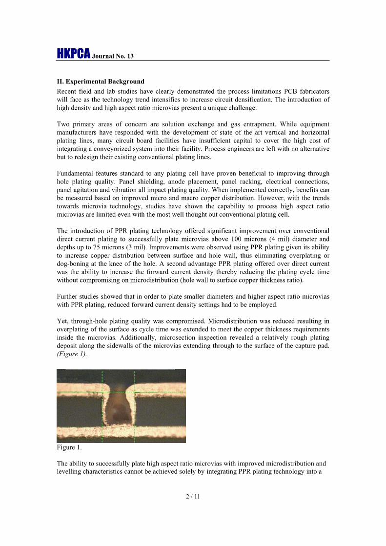
Yet, through-hole plating quality was compromised. Microdistribution was reduced resulting in overplating of the surface as cycle time was extended to meet the copper thickness requirements inside the microvias. Additionally, microsection inspection revealed a relatively rough plating deposit along the sidewalls of the microvias extending through to the surface of the capture pad. (Figure 1).
Figure 1.
The ability to successfully plate high aspect ratio microvias with improved microdistribution and levelling characteristics cannot be achieved solely by integrating PPR plating technology into a
HKPCA Journal No. 13
3 / 11
direct current plating cell with conventional equipment features. Various plating tests and corresponding results to date clearly illustrate a deficiency in the ability to replenish fresh acid copper electrolyte into high aspect ratio microvias. Solution entrapment or gas entrapment caused by poor panel agitation, marginal panel vibration, solution air agitation or a combination of all 3 variables will result in poor plating characteristic. Reduced copper thickness (reduced plating efficiency), rough or burnt plating deposit, plating voids, poor leveling and reduced microdistribution are all defects which can be associated with inadequate solution transfer.To overcome these deficiencies, an improved fluid delivery system was investigated. Eductor technology has been utilized in various electrolytic plating applications including copper, tin and nickel/gold. Various claims have been made confirming the benefits attained using this technology - ability to plate at higher current densities without sacrificing performance, reduced cycle time, airless system to prevent pits or mouse bits, have all been proven in one application or another with success. With these features in mind, it was decided to integrate PPR plating with eductor technology. Specifications governing the installation of the eductor nozzles were based on the recommendations of the supplier as well as field application experiences. However, these recommendations and experiences were limited to through-hole via processing. III. Experimental Objective The goal of this study was to optimize microvia plating performance based on the method of plating (DC v. PPR) and the positioning of the eductor fluid delivery system. Results obtained for the optimized positioning of eductors for microvia plating was baselined against high aspect ratio through-hole vias. The criteria used in the testing to measure performance capability comparing the different plating applications with the various eductor configurations and solution aeration is as follows: Plating thickness / Microdistribution All test panels were micro-sectioned in a number of locations and through hole and microvia plating thicknesses were measured. Copper thickness was measured at the center of the holes (average minimum thickness) and at the outside edge (top and bottom) of the holes (average minimum thickness). From this data percent microdistribution was calculated. Surface appearance All test panels were visually inspected for surface appearance uniformity. The surface appearance was deemed acceptable if the surface appearance was consistently bright or matte. A combination of bright and matte areas was unacceptable, as well as a burnt or rough surface topography. IV. Experimental Procedure A standard experimental design was set-up to determine the optimum position and orientation of a sparger system fitted with eductor nozzles.
The test program was performed in both pulse plate and direct current mode to compare performance capability. A test run utilizing solution aeration was incorporated into the test program as a control.

HKPCA Journal No. 13
4 / 11
Panel #
Eductor Application
Test Vehicle
Plating Mode
1. Aeration Microvia PPR 2. 0゚Paralled Microvia PPR 3. 45゚Diagonal Microvia PPR 4. 90゚Perpendicular Microvia PPR 5. Aeration Microvia DC 6. 0゚Paralled Microvia DC 7. 45゚Diagonal Microvia DC 8. 90゚Perpendicular Microvia DC
Table 1. Eductor Agitation Configuration
Each eductor orientation was configured with a total of 4 eductor nozzles – with two 9.6 mm (0.375”) eductor nozzles positioned on both sides of the cathode.
The 0° sparger was installed directly underneath, parallel and slightly off centered from the cathode position (see Figure 2). The eductor nozzles were positioned upwards to move solution across the surface of the panel. The eductor nozzles are spaced 18 cm apart and the distance between the split sparger pipes is 18 cm. The eductor nozzles were centered around the position of the test panels to be plated. The 45° sparger was installed beneath the anode bars with the eductor nozzles pointed diagonally toward the direction of the cathode position at a 45 angle (see Figure 2). The nozzles are spaced 15 cm apart. The distance between the split sparger pipes is 60 cm. Again, the sparger is centered around the position of the test panels to be plated. The 90° sparger was positioned perpendicular to the cathode placement, spaced 16 cm on center from side to side. (see Figure 2). The eductor nozzles were placed 15 cm apart from top to bottom in the sparger pipe and spaced equal distance across the surface of the test panels to be plated.
Figure 2. Eductor positioning
Test Vehicles Description

HKPCA Journal No. 13
5 / 11
Microvia test panel
Panel thickness: 1.3 mm (0.052”)
This panel was laser drilled with 19 different microvia diameters ranging from 65 – 200 microns (2.5 – 8.0 mils). The depth of the microvia is approximately 100 microns (4 mils). The panel is constructed of high Tg (165 ° C) resin coated copper (RCC) encapsulating di-functional double-sided laminate. The test panel is specifically useful in experimental design evaluations. The small changes in aspect ratio provides the opportunity to collect a range of responses (such as copper thickness) necessary to interpret DOE test results.
Processing of test panels
The test panels were passed through a surface deburr unit prior to wet chemical processing. Desmear and Electroless Copper for the Microvia test panels were processed at a production facility using conventional immersion tank process equipment. The production cycle is summarized in Table 2.
Step #
Process Sequence Temp ( C)
Time (min.)
1. M-Treat BIO 43 5 2. Rinse 2 3. M-Permanganate-P 75 10 4. Rinse(2) 6 5. M-Neuatralizer 43 5 6. Rinse 1 7. M-Conditioner 50 5 8. Rinse 5 9. MACuPrep G-4
Microetch 30 1 micron
removal
10. Rinse 5 11. M-Predip 25 1 12. M-Activate 32 5 13. Rinse(2) 1.5 14. M-Accelerate 50 2.5 15. Rinse 1 16. M-85 Electroless
Copper 46 30
Table 2. Desmear/Electroless Process Cycle.
To ensure complete hole wall electroless coverage in the high aspect ratio through holes and microvias, rack vibration in addition to panel and solution agitation was utilized on each process step.
Following electroless deposition, the test panels were returned to MacDermid’s Customer Service Laboratory based in Waterbury, CT for electroplating. All panels were processed through a preclean cycle consisting of an acid cleaner, microetch and acid dip with appropriate rinsing between stations. The preclean line was equipped with panel agitation, filter pumps and
HKPCA Journal No. 13
6 / 11
vibration to ensure complete hole wall wetting. The process cycle is outlined in Table 3. The electrolytic plating tank used to electroplate the test panels offers features such as panel vibration, panel agitation, solution filtration, computer controls for autodosing chemical additives, solution aeration and the flexibility to interchange the various eductor sparger configurations. Several operating conditions were held constant to eliminate process variations during the plating process. ie. solution flow rate through the eductor nozzles, pulse plate parameters, direct plate parameters, cycle time, panel agitation frequency and stroke distance.
All test panels were electroplated with two plating racks – one on each side of the panel with point contacts on both sides of the panels.
Step #
Process Sequence Temp ( C)
Time (min.)
1. Metex Acid Clean 9271
50 4
2. Rinse 3 3. MACuPrep G-4
Microetch 30 0.25
micron removal
4. Rinse 1 5. Sulfuric Acid Dip 25 1 6. Electrolytic Panel
Plate 25
Table 3. Electroplating Process Cycle.
Pulse Plate and Direct Current Plating Cycles
The pulse plating parameters consisted of a 4step multicycle program. The program is a standard cycle used to benchmark performance level and commonly used for high aspect ratio plating. The forward current density is maintain at a constant amperage, while the reverse current density begins at 3.14x the forward current density and is stepped down to 1x the forward current density. The forward to reverse time ratio is maintained at 20:1.
Forward CD
(ASD)
Reverse CD
(ASD)
Frequenc y (Hz)
Pulse width (msec)
Cycle time
2.5 8.0 48 1.0 36’ 2.5 6.5 48 1.0 12’ 2.5 4.0 48 1.0 6’ 2.5 2.5 200 0.24 6’
Total 60’
Table 4. The 4-step PPR multicycle program
The DC plating cycle was set at 2.0 ASD for a total cycle time of 75 minutes.
In most production facilities, DC plating above 2.5 ASD on aspect ratio greater than 10:1 and microvias less than 100 microns (4 mils) is not common practice. The benefits attained
HKPCA Journal No. 13
7 / 11
by pulse plating are well known and production proven. The ability to plate at higher CD without compromising performance is a clear advantage over conventional DC plating.
Although the CD was reduced from 2.5 ASD to 2.0 ASD for DC plating, the cycle times were adjusted accordingly to ensure equivalent amp-minutes.
Test panel evaluation
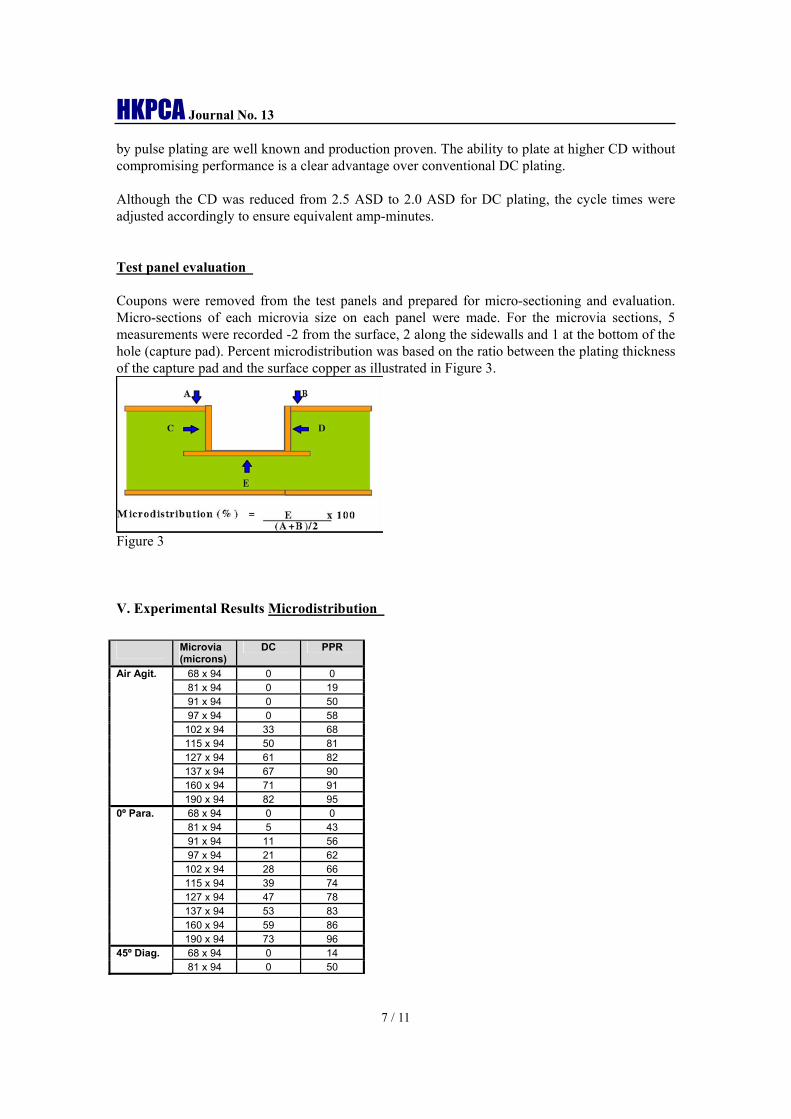
Coupons were removed from the test panels and prepared for micro-sectioning and evaluation. Micro-sections of each microvia size on each panel were made. For the microvia sections, 5 measurements were recorded -2 from the surface, 2 along the sidewalls and 1 at the bottom of the hole (capture pad). Percent microdistribution was based on the ratio between the plating thickness of the capture pad and the surface copper as illustrated in Figure 3.
Figure 3
V. Experimental Results Microdistribution
Microvia (microns)
DC PPR
68 x 94 0 0 81 x 94 0 19 91 x 94 0 50 97 x 94 0 58
102 x 94 33 68 115 x 94 50 81 127 x 94 61 82 137 x 94 67 90 160 x 94 71 91
Air Agit.
190 x 94 82 95 68 x 94 0 0 81 x 94 5 43 91 x 94 11 56 97 x 94 21 62
102 x 94 28 66 115 x 94 39 74 127 x 94 47 78 137 x 94 53 83 160 x 94 59 86
0º Para.
190 x 94 73 96 68 x 94 0 14 45º Diag. 81 x 94 0 50

HKPCA Journal No. 13
8 / 11
91 x 94 0 64 97 x 94 0 77
102 x 94 67 88 115 x 94 83 89 127 x 94 87 94 137 x 94 92 101 160 x 94 97 102
190 x 94 97 100 68 x 94 0 52 81 x 94 34 75 91 x 94 38 93 97 x 94 61 99
102 x 94 65 104 115 x 94 84 110 127 x 94 87 111 137 x 94 90 113 160 x 94 96 116
90º Perp.
190 x 94 98 117
Table 5 Results show a clear benefit of PPR over DC in conventional air agitation (Table 5). Microdistribution improvements ranged from 20 – 100%, depending on the aspect ratio evaluated. Higher aspect ratios showed the most improvement up through the limits of the process.
Figure 4. DC at 102 x 94 micron
Figure 5. PPR at 102 x 94
However, even PPR plating fell short at the highest aspect ratio tested (68 x 94 microns).

HKPCA Journal No. 13
9 / 11
Further improvements were seen with the application of eductors, where the positions at 90º perpendicular offered the best distribution as summarized in Table 6.
Microvia 0º Para. 45º Diag. 90º Perp.
68 x 94 0% 14% 52% 102 x 94 66% 88% 104% 160 x 94 91% 102% 116%
Table 6.
Once again, the most dramatic improvements were seen in high aspect ratio microvias.
Figure 6. 0° Eductor, 68 x 94 micron Figure 10. 45° Eductor, 102 x 94 micron
Figure 7. 45° Eductor, 68 x 94 micron Figure 11. 90° Eductor, 102 x 94 micron

HKPCA Journal No. 13
10 / 11
Figure 8. 90° Eductor, 68 x 94 micron Figure 12. 0° Eductor, 160 x 94 micron
Figure 9. 0° Eductor, 102 x 94 micron Figure 13. 45° Eductor, 160 x 94 micron
Figure 14. 90° Eductor, 160 x 94 micron
Clear advantages were observed with eductor nozzles compared to conventional solution aeration and independent of pulse plate or direct plate mode. Overall, improved microdistribution capability was achieved by combining pulse plate technology and eductor technology in place of conventional solution aeration. Surface Appearance
All test panels were evaluated for surface appearance following electrolytic pulse plating. Several aspects were taken into consideration to determine whether the resulting surface appearance is acceptable: • The surface must be uniform in appearance. • The resulting surface must be classified as bright, semi bright, semi matte or matte. • The surface must not exhibit any signs of burning. • Surface appearance must be consistent between the front and backside of the panel. Plating
Mode Description
Air PPR Uniform semi-matte. 0°Para. PPR Uniform semi-matte. 45°Diag. PPR Uniform semi-matte.

HKPCA Journal No. 13
11 / 11
90°Perp. PPR Uniform semi-matte. Air DC Uniform bright. 0°Para. DC Uniform bright. 45°Diag. DC Uniform bright. 90°Perp. DC Uniform bright.
Table 7. Summarized in table 7, the surface appearance with eductor nozzles was consistent to solution aeration. A uniform semi matte surface was created with pulse plating. In DC mode all test panels exhibited a uniform bright surface. All test panels were plated as panel plating. Both surface conditions would be considered acceptable for subsequent process steps (i.e. dry film lamination) without the necessity of a secondary surface prep cycle.
VI. Conclusion
The test program demonstrated the benefits that can be achieved by integrating PPR plating with eductor technology. While PPR clearly out performed conventional DC plating with and without eductors, high aspect ratio microvias continue to push the capability of the system. Utilizing eductors as the primary fluid delivery system enhanced performance capability in the range of aspect ratios tested. Performance in this study was based on increased plating efficiency inside blind-ended vias. Eductors positioned at 90 degrees, combined with PPR plating, provided a higher level of performance as evidenced by: • Improved microdistribution • Increased copper thickness • Improved levelling capability – eliminate rough plating • Reduced cycle time to achieve required plating thickness • Increased technical capability The results from this testing may lead PCB manufacturers in the direction of improving their solution delivery system. However, while PCB manufacturers may be intrigued by these results, several issues will surface as they begin to explore the possibilities of installing eductors as outlined above into their existing plating lines. Reduced anode to cathode spacing and a continuous anode diaphragm may prove to be a tremendous obstacle for installing eductor nozzles at a 90 degree angle in new or existing vertical hoist plating lines.
Further efforts directed toward enhancing microvia plating capabilities through eductor technology will include: • Solution flow rate • Nozzles pattern and positioning • Equipment Integration