hitachi 42pd6700u plasma tv
TRANSCRIPT

8/12/2019 Hitachi 42PD6700U Plasma TV
http://slidepdf.com/reader/full/hitachi-42pd6700u-plasma-tv 1/79
CAUTION:Before servicing this chassis, it is important that the service technician read the “SafetyPrecautions” and “Product Safety Notices” in this service manual.
ATTENTION: Avant d’effectuer l’entretien du châassis, le technicien doit lire les «Précautions de sécurité»et les «Notices de sécurité du produit» présentés dans le présent manuel.
VORSICHT:Vor Öffnen des Gehäuses hat der Service-Ingenieur die „Sicherheitshinweise“ und „Hinweisezur Produktsicherheit“ in diesem Wartungshandbuch zu lesen.
SERVICE MANUAL
MANUEL D'ENTRETIEN
WARTUNGSHANDBUCH
Data contained within this Servicemanual is subject to alteration forimprovement.
Les données fournies dans le présentmanuel d’entretien peuvent faire l’objetde modifications en vue de perfectionnerle produit.
Die in diesem Wartungshandbuchenthaltenen Spezifikationen können sichzwecks Verbesserungen ändern.
SPECIFICATIONSAND PARTS ARE SUBJECTTO CHANGE FOR IMPROVEMENT
Plasma TV
June 2006
SM012
42PD6700U

8/12/2019 Hitachi 42PD6700U Plasma TV
http://slidepdf.com/reader/full/hitachi-42pd6700u-plasma-tv 2/79
i
TABLE OF CONTENTS
2 SERVICE MENU ITEMS 12.1. SOUND 1 12.2. SOUND 2 12.3. Options 2
2.4. Features 22.5. Teletext 32.6. Tuner Options 3
3 SOFTWARE UPDATE DESCRIPTION 43.1. ANALOG SOFTWARE UPDATE via SCART 43.2. ANALOG SOFTWARE UPDATE via I
2C 5
3.3. EEPROM UPDATE via SCART 64 INTRODUCTION 75 TUNER 76 IF PART (TDA9886) 77 MULTI-STANDARD SOUND PROCESSOR 88 VIDEO SWITCH TEA6415 89 AUDIO AMPLIFIER STAGE WITH TPA3004D2 8
10 POWER SUPPLY (SMPS) 911 MICRO-CONTROLLER 912 SERIAL ACCESS CMOS 4Kx8 (32KBit) EEPROM 24C32A 913 CLASS AB STEREO HEADPHONE DRIVER TDA1308 914 SAW FILTERS 915 IC DESCRIPTIONS 10
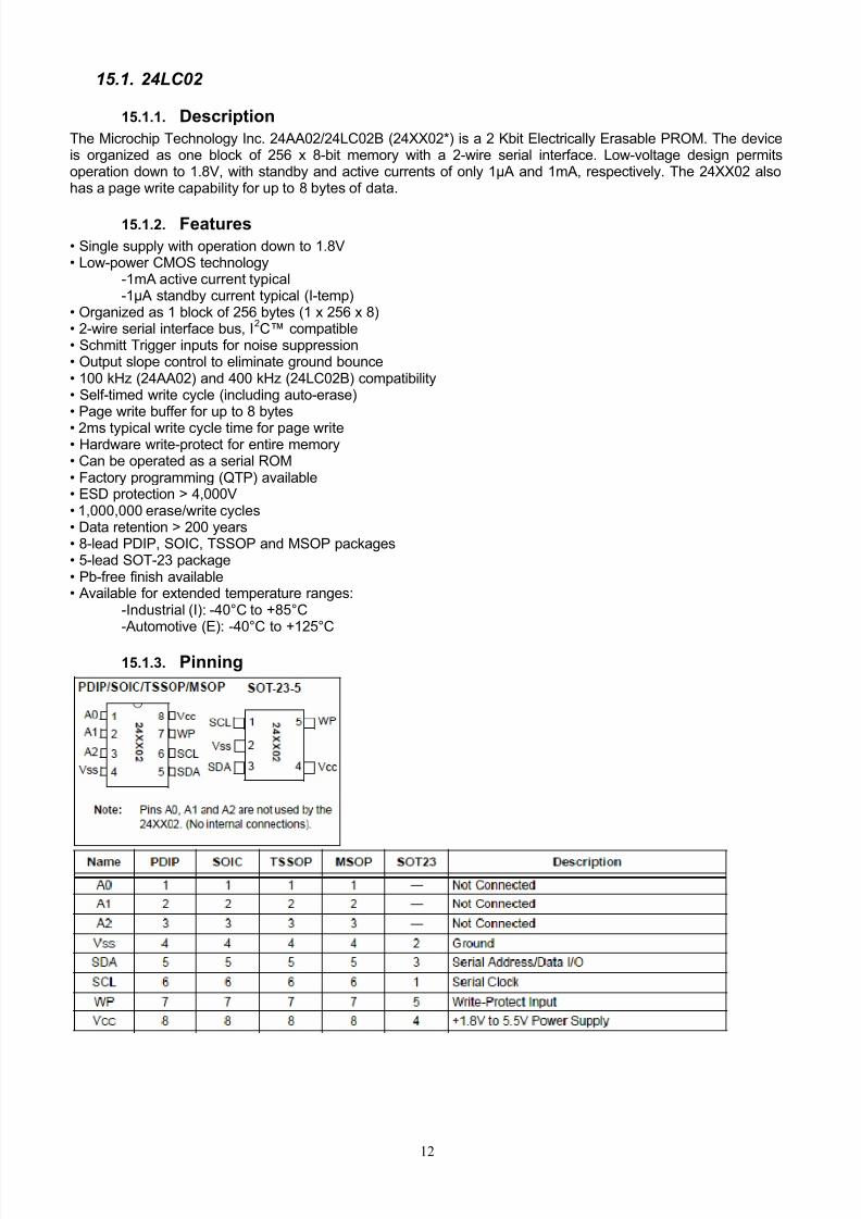
TEA6415C 1015.1. 24LC02 12
15.1.1. Description 1215.1.2. Features 1215.1.3. Pinning 12
15.2. 24C32 1315.2.1. General Description 13
15.2.2. Features 1315.2.3. Pinning 1315.2.4. PIN Function Table 14
15.3. 74LVC14A 1415.3.1. Description 1415.3.2. Features 1415.3.3. Pinning 14
15.4. TEA6420 1515.4.1. Features 1515.4.2. Description 1515.4.3. Pin Connections 15
15.5. CS4334 1515.5.1. Features 15
15.5.2. General Description 1615.5.3. Pin Descriptions 1615.6. GAL16LV8 16
15.6.1. Description 1615.6.2. Features 1615.6.3. Pin connections 17
15.8. K6R4008V1D 1715.8.1. Description 1715.8.2. Features 1715.8.3. Pin Description 18
15.9. KA278R33 1815.9.1. Features 1815.9.2. Description 18
15.10. LM1117 1915.10.1. General Description 1915.10.2. Features 1915.10.3. Applications 19

8/12/2019 Hitachi 42PD6700U Plasma TV
http://slidepdf.com/reader/full/hitachi-42pd6700u-plasma-tv 3/79
ii
15.11. LM317 1915.11.1. General Description 1915.11.2. Features 1915.11.3. Pin Description 20
15.12. LM809 2015.12.1. General Description 2015.12.2. Features 2015.12.3. Pinning 20
15.13. MSP34X1G (MSP3411G) 2015.13.1. Introduction 2115.13.2. Features 21
15.14. M29W040B 2315.14.1. Description 2315.14.2. Features 2315.14.3. Pin Descriptions 24
15.15. MC33202 2415.15.1. General Description 2415.15.2. Features 2415.15.3. Pin Connections 25
15.16. PCF8574 2515.16.1. General Description 25
15.16.2. Features 2515.16.3. Pinning 25
15.17. TSOP1836 2615.17.1. Description 2615.17.2. Features 26
15.18. PI5V330 2615.18.1. General Description 26
15.19. SDA55XX (SDA5550) 2715.19.1. General description 27
15.20. Sil 9993 2715.20.1. General Description 2715.20.2. Features 27
15.21. SN74CB3Q3305 28
15.21.1. General Description 2815.21.2. Features 2815.21.3. Pin Connections 28
15.22. ST24LC21 2815.22.1. Description 2815.22.2. Features 2915.22.3. Pin connections 29
15.23. LM2576 2915.23.1. General Description 2915.23.2. Features 2915.23.3. Pin description 30
15.24. MC34063 3015.24.1. Description 30
15.24.2. Features 3015.24.3. Pin connections 30
15.25. TDA1308 3115.25.1. General Description 3115.25.2. Features 3115.25.3. Pinning 31
15.26. TDA9886 3115.26.1. General Description 3115.26.2. Features 3115.26.3. Pinning 32
15.27. TPA3004D2 3215.27.1. General Description 3215.27.2. Features 3215.27.3. Pinning 33

8/12/2019 Hitachi 42PD6700U Plasma TV
http://slidepdf.com/reader/full/hitachi-42pd6700u-plasma-tv 4/79

8/12/2019 Hitachi 42PD6700U Plasma TV
http://slidepdf.com/reader/full/hitachi-42pd6700u-plasma-tv 5/79
iv
18 APPENDIX A 5318.1. EXPLODED VIEW 73
19 APPENDIX B 5419.1. BLOCK DIAGRAM 5419.2. SCHEMATIC DIAGRAMS 55
19.2.1. Power Board 5519.2.2. Main Board 60
19.2.3. Amplifier Board 6819.2.4. Front AV Board 69
19.3. CIRCUIT BOARDS 7019.4. PCB LAYOUTS 7119.4. CONNECTOR DIAGRAM 72
20 APPENDIX C 7320.1. SPARES PARTLIST 73
8/12/2019 Hitachi 42PD6700U Plasma TV
http://slidepdf.com/reader/full/hitachi-42pd6700u-plasma-tv 6/79
1
2. SERVICE MENU ITEMS
2.1. SOUND 1
a) Menu Subwoofer => If ON, Subwoofer option is available in TV set, and the item isvisible in sound menu, else Subwoofer is not available. Default “ON”.
b) Subwoofer Level (dB) => This value is gain value of Subwoofer output in dB.
-30...12. Default “0” dB.
c) Subwoofer Corner Freq. (x10Hz) => Last low frequency value that is amplified. 5...40.
Default “22” x 10Hz = 220Hz.
d) Menu Equalizer => If ON, visible in sound menu, else invisible. Default “ON”.
e) Menu Headphone => If ON, visible in sound menu, else invisible. Default “ON”.
f) Menu Effect => If ON, visible in sound menu, else invisible. Default “ON”.
g) Menu Wide Sound => If ON, visible in sound menu, else invisible. Default “OFF”.
h) Menu Dynamic Bass => If ON, visible in sound menu, else invisible. Default “ON”.
i) Menu Virtual Dolby => If ON, visible in sound menu, else invisible. Default “ON”.
j) Carrier Mute => If ON, in the absence of an FM carrier the output is muted, else not.
Default “ON”.
k) Virtual Dolby Text => Active if VIRTUAL DOLBY is ON.According to the selection; seen
in sound menu as 3DS or VIRTUAL DOLBY. Default “3DS”.
2.2. SOUND 2
a) AVL => AVL is controlled from this menu by service user. ON/OFF. Default “ON”.
b) Menu AVL => If ON, AVL item is visible in sound menu, and AVL can be controlled from
sound menu by normal user, else AVL is invisible to normal user. ON/OFF. Default “ON”.
c) FM PRESCALE AVL ON => If AVL ON, set value in this item is used as prescale valuefor the related standard. 0...127. Default “29”.
d) NICAM PRESCALE AVL ON => If AVL ON, set value in this item is used as prescale value
for the related standard. 0...127. Default “62”.
e) SCART PRESCALE AVL ON => If AVL ON, set value in this item is used as prescale value
for scart outputs. 0...127. Default “28”.
f) SCART VOLUME AVL ON => If AVL ON, set value in this item is used as volume value
for scart1 and scart2. 0...127. Default “116”.

8/12/2019 Hitachi 42PD6700U Plasma TV
http://slidepdf.com/reader/full/hitachi-42pd6700u-plasma-tv 7/79
2
g) FM PRESCALE AVL OFF => If AVL OFF, set value in this item is used as prescale value
for the related standard. 0...127. Default “15”.
h) NICAM PRESCALE AVL OFF => If AVL OFF, set value in this item is used as
prescale value for the related standard. 0...127. Default “35”.
i) SCART PRESCALE AVL OFF => If AVL OFF, set value in this item is used as
prescale value for scart outputs. 0...127. Default “14”.
j) SCART VOLOUME AVL OFF => If AVL OFF, set value in this item is used as volume
value for scart1 and scart2. 0...127. Default “122”.
2.3. Options
a) Burn-In Mode => If ON, full screen flashes in RED, GREEN, BLUE colors unless
“Menu” button on Remote Control or Keypad is pressed. This property is used to protect the TV
set from burning on the assembly lines in factory. This item becomes automatically OFF, when
First APS item is ON or Factory Reset is pressed. ON/OFF. Default OFF.
b) First APS => This bit is set “ON” in the factory. When the TV set is opened forthe first time it directs the user to make automatic search in both digital and analog modes.
c) APS Volume => After First APS function finishes, the volume of the TV is that value.
Default “10”.
d) AGC (dB) => Tuner AGC value. Default “15”.
e) Power-Up Mode =>Normal, Last State, Stand-by. Default “Last State”
f) PDP Working Hour =>Displays Panel Run time in decimal.
g) Factory Reset => OK to activate. When OK pressed on this item, factory defaults
loaded.
h) Enter Flash Mode =>OK to activate. When OK pressed on this item, flash mode is entered,
SW starts to wait for uploading the new SW.
2.4. Features
a) Blue Background => If ON, Blue Background is visible in Features Menu else not.
Default “ON”.
b) Menu Transparency => If ON, Menu Transparency is visible in Features Menu else not.Default “ON”.
c) Menu Timeout => If ON, Menu Timeout is visible in Features Menu else not. Default
“ON”.
d) Backlight => If ON, Backlight is visible in Features Menu else not.Default “OFF”.
e) Single Tuner => If OFF, two tuners are available on the chassis. Fixed “ON”.
f) Dynamic WB => Default

8/12/2019 Hitachi 42PD6700U Plasma TV
http://slidepdf.com/reader/full/hitachi-42pd6700u-plasma-tv 8/79
3
2.5. Teletext
a) TOP TXT => ON/OFF
b) Fast TXT => ON/OFF
c) Teletext Language => Teletext Language may be controlled from this menu by service
user.
d) Txt Start RF
e) Txt Start Ext
f) Txt Start Mix
g) Menu Teletext Language => If ON, Teletext Language item is visible in Features Menu, and
Teletext Language can be controlled from Features Menu by normal user, else Teletext
Language is invisible to normal user.
2.6. Tuner Options
a) Switch Low Band
b) Switch Mid Band
c) Switch High Band
d) Boundry1 Low Byte
e) Boundry1 High Byte
f) Boundry2 Low Byte
g) Boundry2 High Byte
h) Control Byte
These values need to be filled in the factory acording to the tuner used on the chassis.
i) Store => OK to store; when the values are entered correctly OK needs to be pressed on this
item to store the values.
8/12/2019 Hitachi 42PD6700U Plasma TV
http://slidepdf.com/reader/full/hitachi-42pd6700u-plasma-tv 9/79

8/12/2019 Hitachi 42PD6700U Plasma TV
http://slidepdf.com/reader/full/hitachi-42pd6700u-plasma-tv 10/79
5
3.2. ANALOG SOFTWARE UPDATE via I2C
STEP.1
Enter service menu by pressing the buttons “MENU”,”4”,”7”,”2”,”5” respectively.
STEP.2
Select “OPTIONS” from the service menu and “ENTER FLASH MODE”
STEP.3
Connect the Software Update Tool (17tr15-3) to parellel port of your PC.
STEP.4
Connect one-end of cable to “PL604” socket on the chassis socket MB15 STEP.5
Connect other-end of cable to “PL 2” socket on the Update Tool (17tr15-3)
STEP.6
Run IAPWriter.exe.
STEP.7
Click “load file” and load the required software.

8/12/2019 Hitachi 42PD6700U Plasma TV
http://slidepdf.com/reader/full/hitachi-42pd6700u-plasma-tv 11/79
6
3.3. EEPROM UPDATE via SCART
STEP.1.
Insert the EEROM tool(TR16) to SCART-1
STEP.2.
Enter service menu by pressing the buttons “MENU”,”4”,”7”,”2”,”5” respectively
STEP.3.
Press “YELLOW” colour button on the remote controller.Then you will have two options
STEP.3.a
Press “RED” colour button to copy data of external EEPROM into internal one
STEP.3.b
Press “GREEN” colour button to copy data of internal EEPROM into external one

8/12/2019 Hitachi 42PD6700U Plasma TV
http://slidepdf.com/reader/full/hitachi-42pd6700u-plasma-tv 12/79
7
4. INTRODUCTION
42” Plasma TV is a progressive TV control system with built-in de-interlacer and scaler . It uses a 1024x1024panel with 16:9 aspect ratio.The TV is capable of operation in PAL, SECAM, NTSC (playback) colour standardsand multiple transmission standards as B/G, D/K, I/I’, and L/L’ including German and NICAM stereo. Soundsystem output is supplying 2x10W (10%THD) for stereo 8 speakers. The chassis is equipped with many inputsand outputs allowing it to be used as a center of a media system.
It supports following peripherals:2 SCART sockets1 AV input (CVBS + Stereo Audio)1 SVHS input1 Stereo Headphone input1 Component input (YPbPr + Stereo Audio)1 D-Sub 15 PC input1 HDMI input1 Stereo audio input for PC1 Stereo audio output1 Subwoofer output
5. TUNER The tuners used in the design are combined VHF, UHF tuners suitable for CCIR systems B/G, H, L, L’, I/I’, andD/K. The tuning is available through the digitally controlled I
2C bus (PLL). Below you will find info on one of the
Tuners in use.
General description of UV1316:The UV1316 tuner belongs to the UV 1300 family of tuners, which are designed to meet a wide range ofapplications. It is a combined VHF, UHF tuner suitable for CCIR systems B/G, H, L, L’, I and I’. The low IF outputimpedance has been designed for direct drive of a wide variety of SAW filters with sufficient suppression of tripletransient.
Features of UV1316:1. Member of the UV1300 family small sized UHF/VHF tuners2. Systems CCIR: B/G, H, L, L’, I and I’; OIRT: D/K3. Digitally controlled (PLL) tuning via I
2C-bus
4. Off-air channels, S-cable channels and Hyperband5. World standardised mechanical dimensions and world standard pinning6. Compact size7. Complies to “CENELEC EN55020” and “EN55013”
Pinning:1. Gain control voltage (AGC) : 4.0V, Max: 4.5V2. Tuning voltage
3. I²C-bus address select : Max: 5.5V4. I²C-bus serial clock : Min:-0.3V, Max: 5.5V5. I²C-bus serial data : Min:-0.3V, Max: 5.5V6. Not connected7. PLL supply voltage : 5.0V, Min: 4.75V, Max: 5.5V8. ADC input9. Tuner supply voltage : 33V, Min: 30V, Max: 35V
10. Symmetrical IF output 111. Symmetrical IF output 2
6. IF PART (TDA9886)The TDA9886 is an alignment-free multistandard (PAL, SECAM and NTSC) vision and sound IF signal PLL. Thefollowing figure shows the simplified block diagram of the integrated circuit.
The integrated circuit comprises the following functional blocks:

8/12/2019 Hitachi 42PD6700U Plasma TV
http://slidepdf.com/reader/full/hitachi-42pd6700u-plasma-tv 13/79

8/12/2019 Hitachi 42PD6700U Plasma TV
http://slidepdf.com/reader/full/hitachi-42pd6700u-plasma-tv 14/79
9
10. POWER SUPPLY (SMPS)The DC voltages required at various parts of the chassis are provided by an SMPS transformer controlled by the ICMC44608, which is designed for driving, controlling and protecting switching transistor of SMPS. The transformergenerates 145V for FBT input, +/-14V for audio amplifier, 5V and 3.3V stand by voltage and 8V, 12V and 5V supplies forother different parts of the chassis.
An optocoupler is used to control the regulation of line voltage and stand-by power consumption. There is a regulationcircuit in secondary side. This circuit produces a control voltage according to the changes in 145V DC voltage, via an
optocoupler (TCET1102G) to pin3 of the IC.
During the switch on period of the transistor, energy is stored in the transformer. During the switch off period
energy is fed to the load via secondary winding. By varying switch-on time of the power transistor, it controlseach portion of energy transferred to the second side such that the output voltage remains nearly independentof load variations.
11. MICROCONTROLLERThe Micronas SDA 55xx TV microcontroller is dedicated to 8 bit applications for TV control and provides dedicatedgraphic features designed for modern low class to mid range TV sets. The SDA 55xx provides also an integratedgeneral purposefully 8051-compatible microcontroller with specific hardware features especially suitable in TV sets.The microcontroller core has been enhanced to provide powerful features such as memory banking, data pointers andadditional interrupts, etc. The internal XRAM consists of up to 16 kBytes. The microcontroller provides an internalROM of up to 128 kBytes. ROMless versions can access up to 1 MByte of external RAM and ROM. The 8-bitmicrocontroller runs at 33.33 MHz internal clock. SDA 55xx is realized in 0.25 micron technology with 2.5 V supplyvoltage for the core and 3.3 V for the I/O port pins to make them TTL compatible. Based on the SDA 55xx
microcontroller the MINTS software package was developed and provides dedicated device drivers for many Micronasvideo & audio products and includes a full blown TV control SW for the PEPER application chassis. The SDA 55xx isalso supported with powerful design tools like emulators from Hitex, Kleinhenz, iSystems, the Keil C51 Compiler andTEDIpro OSD development SW by Tara Systems.
12. SERIAL ACCESS CMOS 4Kx8(32KBit)EEPROM 24C32AThe Microchip Technology Inc. 24AA32A/24LC32A(24XX32A*) is a 32 Kbit Electrically Erasable PROM. The device isorganized as four blocks of 8K x 8-bitmemory with a 2-wire serial interface. Low-voltage design permits operationdown to 1.8V, with standby and active currents of only 1µA and 1mA, respectively. It has been developed foradvanced, low-power applications such as personal communications or data acquisition. The 24XX32A also has apage write capability for up to 32 bytes of data. Functional address lines allow up to eight devices on the same bus, forup to 256Kbits address space.
13. CLASS AB STEREO HEADPHONE DRIVER TDA1308The TDA1308 is an integrated class AB stereo headphone driver contained in a DIP8 plastic package. Thedevice is fabricated in a 1 mm CMOS process and has been primarily developed for portable digital audioapplications.
14. SAW FILTERSK9656M:Standard:• B/G• D/K• I• L/L’
Features• TV IF audio filter with two channels• Channel 1 (L’) with one pass band for sound carriers at 40.40 MHz (L’) and 39.75 MHz (L’- NICAM)• Channel 2 (B/G, D/K, L, I) with one pass band for sound carriers between 32.35 MHz and 33.40 MHz
Terminals• Tinned CuFe alloy
Pin configuration1 Input2 Switching input3 Chip carrier - ground4 Output
5 Output

8/12/2019 Hitachi 42PD6700U Plasma TV
http://slidepdf.com/reader/full/hitachi-42pd6700u-plasma-tv 15/79
10
K3958M:Standard:
• B/G• D/K• I• L/L’
Features
• TV IF video filter with Nyquist slopes at 33.90 MHz and 38.90 MHz
• Constant group delay
TerminalsTinned CuFe alloy
Pin configuration1 Input2 Input - ground3 Chip carrier - ground4 Output5 Output
15. IC DESCRIPTIONSTEA6415C24LC0224C3274LVC14A
TEA6420DCS4334
GAL16LV8K6R4008V1KA278R33LM1117LM317TLM809
MSP3411GM29W040BMC33202PCF8574TSOP1836PI5V330
SDA5550SII9993
SN74CB3Q3305ST24LC21LM2576MC34063TDA1308TDA9886T
TPA3004D2µPA672TVPC3230DMAD4868ASVP EX-59B
TEA6415C
General Description
The main function of the IC is to switch 8 video input sources on 6 outputs. Each output can be switched on onlyone of each input. On each input an alignment of the lowest level of the signal is made (bottom of synch. top forCVBS or black level for RGB signals). Each nominal gain between any input and output is 6.5dB. For D2MAC or
Chroma signal the alignment is switched off by forcing, with an external resistor bridge, 5 VDC
on the input. Eachinput can be used as a normal input or as a MAC or Chroma input (with external resistor bridge). All theswitching possibilities are changed through the BUS. Driving 75 load needs an external transistor. It is possible

8/12/2019 Hitachi 42PD6700U Plasma TV
http://slidepdf.com/reader/full/hitachi-42pd6700u-plasma-tv 16/79
11
to have the same input connected to several outputs. The starting configuration upon power on (power supply: 0to 10V) is undetermined. In this case, 6 words of 16 bits are necessary to determine one configuration. In othercase, 1 word of 16 bits is necessary to determine one configuration.Features
• 20MHz Bandwidth• Cascadable with another TEA6415C (Internal address can be changed by pin 7 voltage)• 8 Inputs (CVBS, RGB, MAC, CHROMA,...)• 6 Outputs• Possibility of MAC or chroma signal for each input by switching-off the clamp with an external resistor bridge
• Bus controlled• 6.5dB gain between any input and output• 55dB crosstalk at 5mHz• Fully ESD protectedPinning
1. Input : Max : 2Vpp, Input Current: 1mA, Max : 3mA2. Data : Low level : -0.3V Max: 1.5V,
High level : 3.0V Max : Vcc+0.5V3. Input : Max : 2Vpp, Input Current: 1mA, Max : 3mA4. Clock : Low level : -0.3V Max: 1.5V,
High level : 3.0V Max : Vcc+0.5V5. Input : Max : 2Vpp, Input Current: 1mA, Max : 3mA6. Input : Max : 2Vpp, Input Current: 1mA, Max : 3mA
7. Prog8. Input : Max : 2Vpp, Input Current: 1mA, Max: 3mA9. Vcc : 12V10. Input : Max : 2Vpp, Input Current: 1mA, Max : 3mA11. Input : Max : 2Vpp, Input Current: 1mA, Max : 3mA12. Ground13. Output : 5.5Vpp, Min : 4.5Vpp14. Output : 5.5Vpp, Min : 4.5Vpp15. Output : 5.5Vpp, Min : 4.5Vpp16. Output : 5.5Vpp, Min : 4.5Vpp17. Output : 5.5Vpp, Min : 4.5Vpp18. Output : 5.5Vpp, Min : 4.5Vpp19. Ground
20. Input : Max : 2Vpp, Input Current : 1mA, Max : 3mA
8/12/2019 Hitachi 42PD6700U Plasma TV
http://slidepdf.com/reader/full/hitachi-42pd6700u-plasma-tv 17/79

8/12/2019 Hitachi 42PD6700U Plasma TV
http://slidepdf.com/reader/full/hitachi-42pd6700u-plasma-tv 18/79
13
15.2. 24C32
15.2.1. General Description
The Microchip Technology Inc. 24C32 is a 4K x 8 (32K bit) Serial Electrically Erasable PROM. This device hasbeen developed for advanced, low power applications such as personal communications or data acquisition.The 24C32 features an input cache for fast write loads with a capacity of eight 8-byte pages, or 64 bytes. It also
features a fixed 4K-bit block of ultra-high endurance memory for data that changes frequently. The 24C32 iscapable of both random and sequential reads up to the 32K boundary. Functional address lines allow up to 8 -24C32 devices on the same bus, for up to 256K bits address space. Advanced CMOS technology makes thisdevice ideal for low-power non-volatile code and data applications.
15.2.2. Features
• Voltage operating range: 4.5V to 5.5V- Peak write current 3 mA at 5.5V- Maximum read current 150µA at 5.5V- Standby current 1µA typical
• Industry standard two-wire bus protocol, I2C™ compatible
-Including 100 kHz and 400 kHz modes• Self-timed write cycle (including auto-erase)
• Power on/off data protection circuitry• Endurance:
- 10,000,000 Erase/Write cycles guaranteed for High Endurance Block- 10,000,000 E/W cycles guaranteed for Standard Endurance Block
• 8 byte page, or byte modes available• 1 page x 8 line input cache (64 bytes) for fast writeloads• Schmitt trigger, filtered inputs for noise suppression• Output slope control to eliminate ground bounce• 2 ms typical write cycle time, byte or page• Up to 8 chips may be connected to the same bus for up to 256K bits total memory• Electrostatic discharge protection > 4000V• Data retention > 200 years
• Temperature ranges:-Commercial (C): 0°C to +70°C-Industrial (I): -40°C to +85°C
15.2.3. Pinning

8/12/2019 Hitachi 42PD6700U Plasma TV
http://slidepdf.com/reader/full/hitachi-42pd6700u-plasma-tv 19/79

8/12/2019 Hitachi 42PD6700U Plasma TV
http://slidepdf.com/reader/full/hitachi-42pd6700u-plasma-tv 20/79
15
15.4. TEA6420
15.4.1. Features
• 5 Stereo Inputs• 4 Stereo Outputs• Gain Control 0/2/4/6dB/Mute for each Output• Cascadable (2 different addresses)• Serial Bus Controlled• Very low Noise• Very low Distortion
15.4.2. DescriptionThe TEA6420 switches 5 stereo audio inputs on4stereo outputs. All the switching possibilities are changedthrough the I
2C bus.
15.4.3. Pin Connections
15.5. CS4334
15.5.1. Features
• Complete Stereo DAC System: Interpolation, D/A, Output Analog Filtering• 24-Bit Conversion

8/12/2019 Hitachi 42PD6700U Plasma TV
http://slidepdf.com/reader/full/hitachi-42pd6700u-plasma-tv 21/79
16
• 96 dB Dynamic Range
• -88 dB THD+N
• Low Clock Jitter Sensitivity
• Single +5V Power Supply
• Filtered Line Level Outputs
• On-Chip Digital De-emphasis
• Popgaurd® Technology
• Functionally Compatible with CS4330/31/33
15.5.2. General DescriptionThe CS4334 family members are complete, stereo digital-to-analog output systems including interpolation, 1-bitD/A conversion and output analog filtering in an 8-pinpackage. The CS4334/5/6/7/8/9 support all major audiodata interface formats, and the individual devices differ only in the supported interface format. The CS4334family is based on delta-sigma modulation, where the modulator output controls the reference voltage input toan ultra-linear analog low-pass filter. This architecture allows for infinite adjustment of sample rate between 2kHz and 100 kHz simply by changing the master clock frequency. The CS4334 family contains on-chip digitalde-emphasis, operates from a single +5V power supply, and requires minimal support circuitry. These featuresare ideal for set-top boxes, DVD players, SVCD players, and A/V receivers.
15.5.3. Pin Descriptions
15.6. GAL16LV8
15.6.1. Description
The GAL16LV8D, at 3.5 ns maximum propagation delay time, provides the highest speed performance availablein the PLD market. The GAL16LV8C can interface with both 3.3V and 5Vsignal levels. The GAL16LV8 ismanufactured using Lattice Semiconductor's advanced 3.3V E
2CMOS process, which combines CMOS with
Electrically Erasable (E2) floating gate technology. High speed erase times (<100ms) allow the devices to be
reprogrammed quickly and efficiently.The 3.3V GAL16LV8 uses the same industry standard 16V8 architecture as its 5V counterpart and supports allarchitectural features such as combinatorial or registered macrocell operations.Unique test circuitry and reprogrammable cells allow complete AC, DC, and functional testing duringmanufacture. As a result, Lattice Semiconductor delivers 100% field programmability and functionality of allGAL products. In addition, 100 erase/write cycles and data retention in excess of 20 years are specified.
15.6.2. Features
• HIGH PERFORMANCE E2CMOS® TECHNOLOGY- 3.5 ns Maximum Propagation Delay- Fmax = 250 MHz

8/12/2019 Hitachi 42PD6700U Plasma TV
http://slidepdf.com/reader/full/hitachi-42pd6700u-plasma-tv 22/79
17
- 2.5 ns Maximum from Clock Input to Data Output- UltraMOS® Advanced CMOS Technology
• 3.3V LOW VOLTAGE 16V8 ARCHITECTURE- JEDEC-Compatible 3.3V Interface Standard- 5V Compatible Inputs- I/O Interfaces with Standard 5V TTL Devices (GAL16LV8C)
• ACTIVE PULL-UPS ON ALL PINS (GAL16LV8D Only)• E2 CELL TECHNOLOGY
- Reconfigurable Logic
- Reprogrammable Cells- 100% Tested/100% Yields- High Speed Electrical Erasure (<100ms)- 20 Year Data Retention
• EIGHT OUTPUT LOGIC MACROCELLS- Maximum Flexibility for Complex Logic Designs- Programmable Output Polarity
• PRELOAD AND POWER-ON RESET OF ALL REGISTERS- 100% Functional Testability
• APPLICATIONS INCLUDE:- Glue Logic for 3.3V Systems- DMA Control- State Machine Control
- High Speed Graphics Processing- Standard Logic Speed Upgrade
• ELECTRONIC SIGNATURE FOR IDENTIFICATION• LEAD-FREE PACKAGE OPTIONS
15.6.3. Pin connections
15.7.
15.8. K6R4008V1D
15.8.1. DescriptionThe K6R4008V1D is a 4,194,304-bit high-speed Static Random Access Memory organized as 524,288 words by8 bits. TheK6R4008V1D uses 8 common input and output lines and has an output enable pin which operatesfaster than address access time at read cycle. The device is fabricated using SAMSUNG s advanced CMOSprocess and designed for high-speed circuit technology. It is particularly well suited for use in high-density high-speed system applications. The K6R4008V1D is packaged in a 400 mil 36-pin plastic SOJ and 44-pin plasticTSOP type II.
15.8.2. Features
• Fast Access Time 8, 10ns(Max.)• Low Power Dissipation
- Standby (TTL) : 20mA(Max.)
(CMOS) : 5mA(Max.)- Operating K6R4008V1D-08 : 80mA(Max.)

8/12/2019 Hitachi 42PD6700U Plasma TV
http://slidepdf.com/reader/full/hitachi-42pd6700u-plasma-tv 23/79
18
K6R4008V1D-10 : 65mA(Max.)• Single 3.3 ±0.3V Power Supply• TTL Compatible Inputs and Outputs• Fully Static Operation
- No Clock or Refresh required• Three State Outputs• Center Power/Ground Pin Configuration• Standard Pin Configuration
K6R4008V1D-J : 36-SOJ-400
K6R4008V1D-K : 36-SOJ-400(Lead-Free)K6R4008V1D-T : 44-TSOP2-400BFK6R4008V1D-U : 44-TSOP2-400BF(Lead-Free)
• Operating in Commercial and Industrial Temperature range.
15.8.3. Pin Description
15.9. KA278R33
15.9.1. Features
• 2A / 3.3V Output low dropout voltage regulator• TO220 Full-Mold package (4PIN)• Overcurrent protection, Thermal shutdown• Overvoltage protection, Short-Circuit protection• With output disable function
15.9.2. DescriptionThe KA278R33 is a low-dropout voltage regulator suitable for various electronic equipments. It providesconstant voltage power source with TO-220 4 lead full mold package. Dropout voltage of KA278R33 is below

8/12/2019 Hitachi 42PD6700U Plasma TV
http://slidepdf.com/reader/full/hitachi-42pd6700u-plasma-tv 24/79
19
0.5V in full rated current (2A). This regulator has various function such as peak current protection, thermal shutdown, overvoltage protection and output disable function.
15.10. LM1117
15.10.1. General Description
The LM1117 is a series of low dropout voltage regulators with a dropout of 1.2V at 800mA of load current. It has the same pin-out as National Semiconductor’s industry standard LM317. The LM1117 is available in an adjustable version, which
can set the output voltage from 1.25V to 13.8V with only two external resistors. In addition, it is also available in five fixedvoltages, 1.8V, 2.5V, 2.85V, 3.3V, and 5V.
The LM1117 offers current limiting and thermal shutdown. Its circuit includes a zener trimmed bandgapreference to as-sure output voltage accuracy to within ±1%. The LM1117 series is available in SOT-223, TO-220, and TO-252 D-PAK packages. A minimum of 10µF tantalum capacitor is required at the output to improvethe transient response and stability.
15.10.2. Features
• Available in 1.8V, 2.5V, 2.85V, 3.3V, 5V, and Adjustable Versions• Space Saving SOT-223 Package
• Current Limiting and Thermal Protection• Output Current 800mA• Line Regulation 0.2% (Max)• Load Regulation 0.4% (Max)• Temperature Range— LM1117 0°C to 125°C— LM1117I -40°C to 125°C
15.10.3. Applications
• 2.85V Model for SCSI-2 Active Termination• Post Regulator for Switching DC/DC Converter• High Efficiency Linear Regulators• Battery Charger• Battery Powered InstrumentationConnection Diagrams
15.11. LM317
15.11.1. General DescriptionThis monolithic integrated circuit is an adjustable 3-terminal positive voltage regulator designed to supply morethan 1.5A of load current with an output voltage adjustable over a 1.2 to 37V. It employs internal current limiting,thermal shut-down and safe area compensation.
15.11.2. Features
• Output Current In Excess of 1.5A• Output Adjustable Between 1.2V and 37V• Internal Thermal Overload Protection• Internal Short Circuit Current Limiting• Output Transistor Safe Operating Area Compensation• TO-220 Package

8/12/2019 Hitachi 42PD6700U Plasma TV
http://slidepdf.com/reader/full/hitachi-42pd6700u-plasma-tv 25/79
20
15.11.3. Pin Description
15.12. LM809
15.12.1. General Description
The LM809/810 microprocessor supervisory circuits can be used to monitor the power supplies in microprocessor anddigital systems. They provide a reset to the microprocessor during power-up, power-down and brown-out conditions.The function of the LM809/810 is to monitor the VCC supply voltage, and assert a reset signal whenever this voltagedeclines below the factory-programmed reset threshold. The reset signal remains asserted for 240 ms after VCC risesabove the threshold. The LM809 has an active-low RESET output, while the LM810 has an active-high RESET output.Seven standard reset voltage options are available, suitable for monitoring 5V, 3.3V, and 3V supply voltages. With a
low supply current of only 15µA, the LM809/810 are ideal for use in portable equipment.
15.12.2. Features
• Precise monitoring of 3V, 3.3V, and 5V supply voltages
• Superior upgrade to MAX809/810
• Fully specified overtemperature
• 140 ms min. Power-On Reset pulse width, 240 ms typical
Active-low RESET Output(LM809) Active-high RESET Output(LM810)
• Guaranteed RESET Output valid for VCC1V
• Low Supply Current, 15µAtyp
• Power supply transient immunity
15.12.3. Pinning
15.13. MSP34X1G (MSP3411G)
Multistandard Sound Processor Family

8/12/2019 Hitachi 42PD6700U Plasma TV
http://slidepdf.com/reader/full/hitachi-42pd6700u-plasma-tv 26/79
21
15.13.1. Introduction
The MSP 34x1G family of single-chip Multistandard Sound Processors covers the sound processing of allanalog TV-Standards worldwide, as well as the NICAM digital sound standards. The full TV sound processing,starting with analog sound IF signal-in, down to processed analog AF-out, is performed on a single chip. Figureshows a simplified functional block diagram of the MSP 34x1G.The MSP 34x1G has all functions of the MSP 34x0G with the addition of a virtual surround sound feature.Surround sound can be reproduced to a certain extent with two loudspeakers. The MSP 34x1G includes theMicronas virtualizer algorithm “3D-PANORAMA” which has been approved by the Dolby 1) Laboratories for withthe "Virtual Dolby Surround" technology. In addition, the MSP 34x1G includes the “PAN-ORAMA” algorithm.
These TV sound processing ICs include versions for processing the multichannel television sound (MTS) signal conformingto the standard recommended by the Broadcast Television Systems Committee (BTSC). The DBX noise reduction, oralternatively, Micronas Noise Reduction (MNR) is performed alignment free.
Other processed standards are the Japanese FM-FM multiplex standard (EIA-J) and the FM Stereo Radiostandard.Current ICs have to perform adjustment procedures in order to achieve good stereo separation for BTSC andEIA-J. The MSP 34x1G has optimum stereo performance without any adjustments.The MSP 34x1G has built-in automatic functions: The IC is able to detect the actual sound standard automat-ically (Automatic Standard Detection). Furthermore, pilot levels and identification signals can be evaluatedinternally with subsequent switching between mono/stereo/bilingual; no I 2 C interaction is necessary (AutomaticSound Selection).
Source SelectI2S bus interface consists of five pins:
1. I2S_DA_IN1, I2S_DA_IN2: For input, four channels (two channels per line, 2*16 bits) per sampling cycle (32kHz) are transmitted.2. I2S_DA_OUT: For output, two channels (2*16 bits) per sampling cycle (32 kHz) are transmitted.3. I2S_CL: Gives the timing for the transmission of I
2S serial data (1.024 MHz).
4. I2S_WS: The I2S_WS word strobe line defines the left and right sample.
15.13.2. Features
• Standard Selection with single I2C transmission
• Automatic Standard Detection of terrestrial TV standards• Automatic Sound Selection (mono/stereo/bilingual), new registers MODUS, STATUS
• Two selectable sound IF (SIF) inputs• Automatic Carrier Mute function• Interrupt output programmable (indicating status change)• Loudspeaker / Headphone channel with volume, balance, bass, treble, loudness
• AVC: Automatic Volume Correction• Subwoofer output with programmable low-pass and complementary high-pass filter
• 5-band graphic equalizer for loudspeaker channel• Spatial effect for loudspeaker channel• Four Stereo SCART (line) inputs, one Mono input; two Stereo SCART outputs

8/12/2019 Hitachi 42PD6700U Plasma TV
http://slidepdf.com/reader/full/hitachi-42pd6700u-plasma-tv 27/79
22
• Complete SCART in/out switching matrix• Two I2
S inputs; one I2S output
• Dolby Pro Logic with DPL 351xA coprocessor
• All analog FM-Stereo A2 and satellite standards; AM-SECAM L standard• Simultaneous demodulation of (very) high-deviation FM-Mono and NICAM• Adaptive deemphasis for satellite (Wegener-Panda, acc. to ASTRA specification)• ASTRA Digital Radio (ADR) together with DRP 3510A• All NICAM standards
• Korean FM-Stereo A2 standard
Pin connections
NC = not connected; leave vacant
LV = if not used, leave vacantOBL = obligatory; connect as described in circuit diagramDVSS: if not used, connect to DVSS AHVSS: connect to AHVSS
Pin No. Pin Name TypeConnection(if not used)
Short Description
PLCC68-pin
PSDIP64-pin
PSDIP52-pin
PQFP80-pin
PLQFP64-pin
1 16 14 9 8 ADR_WS OUT LV ADR word strobe
2 - - - - NC LV Not connected
3 15 13 8 7 ADR_DA OUT LV ADR Data Output
4 14 12 7 6 I2S_DA_IN1 IN LV I2S1 data input
5 13 11 6 5 I2S_DA_OUT OUT LV I2S data output
6 12 10 5 4 I2S_WS IN/OUT LV I2S word strobe
7 11 9 4 3 I2S_CL IN/OUT LV I2S clock
8 10 8 3 2 I2C_DA IN/OUT OBL I2C data
9 9 7 2 1 I2C_CL IN/OUT OBL I2C clock
10 8 - 1 64 NC LV Not connected
11 7 6 80 63 STANDBYQ IN OBL Stand-by (low-active)
12 6 5 79 62 ADR_SEL IN OBL I2C bus address select
13 5 4 78 61 D_CTR_I/O_0 IN/OUT LV D_CTR_I/O_0
14 4 3 77 60 D_CTR_I/O_1 IN/OUT LV D_CTR_I/O_115 3 - 76 59 NC LV Not connected
16 2 - 75 58 NC LV Not connected
17 - - - - NC LV Not connected
18 1 2 74 57 AUD_CL_OUT OUT LV Audio clock output(18.432 MHz)
19 64 1 73 56 TP LV Test pin
20 63 52 72 55 XTAL_OUT OUT OBL Crystal oscillator
21 62 51 71 54 XTAL_IN IN OBL Crystal oscillator
22 61 50 70 53 TESTEN IN OBL Test pin
23 60 49 69 52 ANA_IN2+ IN AVSS via56 pF/LV
IF Input 2 (can be leftvacant, only if IF input 1 isalso not in use)
24 59 48 68 51 ANA_IN- IN AVSS via56 pF/LV
IF common (can be leftvacant, only if IF input 1 isalso not in use)
25 58 47 67 50 ANA_IN1+ IN LV IF input 126 57 46 66 49 AVSUP OBL Analog power supply 5V
- - - 65 - AVSUP OBL Analog power supply 5V
- - - 64 - NC LV Not connected
- - - 63 - NC LV Not connected
27 56 45 62 48 AVSS OBL Analog ground
- - - 61 - AVSS OBL Analog ground
28 55 44 60 47 MONO_IN IN LV Mono input
- - - 59 - NC LV Not connected
29 54 43 58 46 VREFTOP OBLReference voltage IF A/Dconverter
30 53 42 57 45 SC1_IN_R IN LV SCART 1 input, right
31 52 41 56 44 SC1_IN_L IN LV SCART 1 input, left
32 51 - 55 43 ASG1 AHVSS Analog Shield Ground 1
33 50 40 54 42 SC2_IN_R IN LV SCART 2 input, right
34 49 39 53 41 SC2_IN_L IN LV SCART 2 input, left35 48 - 52 40 ASG2 AHVSS Analog Shield Ground 2
36 47 38 51 39 SC3_IN_R IN LV SCART 3 input, right

8/12/2019 Hitachi 42PD6700U Plasma TV
http://slidepdf.com/reader/full/hitachi-42pd6700u-plasma-tv 28/79
23
37 46 37 50 38 SC3_IN_L IN LV SCART 3 input, left
38 45 - 49 37 ASG4 AHVSS Analog Shield Ground 4
39 44 - 48 36 SC4_IN_R IN LV SCART 4 input, right
40 43 - 47 35 SC4_IN_L IN LV SCART 4 input, left
41 - - 46 - NC LV or AHVSS Not connected
42 42 36 45 34 AGNDC OBL Analog reference voltage
43 41 35 44 33 AHVSS OBL Analog ground
- - - 43 - AHVSS OBL Analog ground
- - - 42 - NC LV Not connected
- - - 41 - NC LV Not connected
44 40 34 40 32 CAPL_M OBL Volume capacitor MAIN
45 39 33 39 31 AHVSUP OBL Analog power supply 8V46 38 32 38 30 CAPL_A OBL Volume capacitor AUX
47 37 31 37 29 SC1_OUT_L OUT LV SCART output 1, left
48 36 30 36 28 SC1_OUT_R OUT LV SCART output 1, right
49 35 29 35 27 VREF1 OBL Reference ground 1
50 34 28 34 26 SC2_OUT_L OUT LV SCART output 2, left
51 33 27 33 25 SC2_OUT_R OUT LV SCART output 2, right
52 - - 32 - NC LV Not connected
53 32 - 31 24 NC LV Not connected
54 31 26 30 23 DACM_SUB OUT LV Subwoofer output
55 30 - 29 22 NC LV Not connected
56 29 25 28 21 DACM_L OUT LV Loudspeaker out, left
57 28 24 27 20 DACM_R OUT LV Loudspeaker out, right
58 27 23 26 19 VREF2 OBL Reference ground 2
59 26 22 25 18 DACA_L OUT LV Headphone out, left
60 25 21 24 17 DACA_R OUT LV Headphone out, right- - - 23 - NC LV Not connected
- - - 22 - NC LV Not connected
61 24 20 21 16 RESETQ IN OBL Power-on-reset
62 23 - 20 15 NC LV Not connected
63 22 - 19 14 NC LV Not connected
64 21 19 18 13 NC LV Not connected
65 20 18 17 12 I2S_DA_IN2 IN LV I2S2-data input
66 19 17 16 11 DVSS OBL Digital ground
- - - 15 - DVSS OBL Digital ground
- - - 14 - DVSS OBL Digital ground
67 18 16 13 10 DVSUP OBL Digital power supply 5V
- - - 12 - DVSUP OBL Digital power supply 5V
- - - 11 - DVSUP OBL Digital power supply 5V
68 17 15 10 9 ADR_CL OUT LV ADR clock
15.14. M29W040B
15.14.1. Description
The M29W040B is a 4 Mbit (512Kb x8) non-volatile memory that can be read, erased and reprogrammed. These operationscan be performed using a single low voltage (2.7 to 3.6V) supply. On power-up the memory defaults to its Read modewhere it can be read in the same way as a ROM or EPROM. The M29W040B is fully backward compatible with theM29W040.The memory is divided into blocks that can be erased independently so it is possible to preserve valid data whileold data is erased. Each block can be protected independently to prevent accidental Program or Erase commands from
modifying the memory. Program and Erase commands are writ-ten to the Command Interface of the memory. An on-chipProgram/Erase Controller simplifies the process of programming or erasing the memory by taking care of all of the specialoperations that are required to update the memory contents. The end of a program or erase operation can be detected andany error conditions identified. The command set required to control the memory is consistent with JEDEC standards. ChipEnable, Output Enable and Write Enable signals control the bus operation of the memory. They allow simple connection tomost microprocessors, often without additional logic.
15.14.2. Features
• SINGLE 2.7 to 3.6V SUPPLY VOLTAGE for PROGRAM, ERASE and READ OPERATIONS• ACCESS TIME: 55ns• PROGRAMMING TIME
- 10µs per Byte typical8• UNIFORM 64 Kbytes MEMORY BLOCKS• PROGRAM/ERASE CONTROLLER
- Embedded Byte Program algorithm- Embedded Multi-Block/Chip Erase algorithm- Status Register Polling and Toggle Bits

8/12/2019 Hitachi 42PD6700U Plasma TV
http://slidepdf.com/reader/full/hitachi-42pd6700u-plasma-tv 29/79
24
• ERASE SUSPEND and RESUME MODES- Read and Program another Block during Erase Suspend
• UNLOCK BYPASS PROGRAM COMMAND- Faster Production/Batch Programming
• LOW POWER CONSUMPTION- Standby and Automatic Standby
• 100,000 PROGRAM/ERASE CYCLES per BLOCK• 20 YEARS DATA RETENTION
- Defectivity below 1 ppm/year
• ELECTRONIC SIGNATURE- Manufacturer Code: 20h- Device Code: E3h
15.14.3. Pin Descriptions
15.15. MC33202
15.15.1. General Description
The MC33201/2/4 family of operational amplifiers provide rail
to
rail operation on both the input and output.The inputs can be driven as high as 200mV beyond the supply rails without phase reversal on the outputs, andthe output can swing within 50 mV of each rail. This railtorail operation enables the user to make full use ofthe supply voltage range available. It is designed to work at very low supply voltages (±0.9 V) yet can operatewith a supply of up to +12V and ground. Output current boosting techniques provide a high output currentcapability while keeping the drain current of the amplifier to a minimum. Also, the combination of low noise anddistortion with a high slew rate and drive capability make this an ideal amplifier for audio applications.
15.15.2. Features
• Low Voltage, Single Supply Operation (+1.8 V and Ground to +12 V and Ground)• Input Voltage Range Includes both Supply Rails• Output Voltage Swings within 50 mV of both Rails• No Phase Reversal on the Output for Over driven Input Signals
• High Output Current (ISC = 80 mA, Typ)• Low Supply Current (ID = 0.9 mA, Typ)• 600 Output Drive Capability• Extended Operating Temperature Ranges (40° to +105°C and 55° to +125°C)• Typical Gain Bandwidth Product = 2.2 MHz• PbFree Packages are Available

8/12/2019 Hitachi 42PD6700U Plasma TV
http://slidepdf.com/reader/full/hitachi-42pd6700u-plasma-tv 30/79
25
15.15.3. Pin Connections
15.16. PCF8574
15.16.1. General Description
The PCF8574 is a silicon CMOS circuit. It provides general purpose remote I/O expansion for most microcontrollerfamilies via the two-line bidirectional bus (I
2C).The device consists of an 8-bit quasi-bidirectional port and an I
2C-bus
interface. The PCF8574 has a low current consumption and includes latched outputs with high current drive capability for
directly driving LEDs. It also possesses an interrupt line (INT) which can be connected to the interrupt logic of the
microcontroller. By sending an interrupt signal on this line, the remote I/O can inform the microcontroller if there isincoming data on its ports without having to communicate via the I2C-bus. This means that the PCF8574 can remain a
simple slave device.
15.16.2. Features
• Operating supply voltage 2.5 to 6V• Low standby current consumption of 10 µA maximum• I
2C to parallel port expander
• Open-drain interrupt output• 8-bit remote I/O port for the I
2C-bus
• Compatible with most microcontrollers• Latched outputs with high current drive capability for directly driving LEDs• Address by 3 hardware address pins for use of up to 8 devices (up to 16 with PCF8574A)
• DIP16, or space-saving SO16 or SSOP20 packages.
15.16.3. Pinning

8/12/2019 Hitachi 42PD6700U Plasma TV
http://slidepdf.com/reader/full/hitachi-42pd6700u-plasma-tv 31/79
26
15.17. TSOP1836
15.17.1. Description
The TSOP18.– series are miniaturized receivers for infrared remote control systems. PIN diode and preamplifierare assembled on lead frame, the epoxy package is designed as IR filter. Carrier frequency for TSOP1836 is 36kHz.The demodulated output signal can directly be decoded by a microprocessor. The main benefit is the reliable
function even in disturbed ambient and the protection against uncontrolled output pulses.
15.17.2. Features
• Photo detector and preamplifier in one package• Internal filter for PCM frequency• TTL and CMOS compatibility• Output active low• Improved shielding against electrical field disturbance• Suitable burst length .6 cycles/burst
Special Features• Small size package
• Enhanced immunity against all kinds of disturbance light• No occurrence of disturbance pulses at the output• Short settling time after power on (<200_s)
15.18. PI5V330
15.18.1. General Description
The PI5V330 is well suited for video applications when switching composite or RGB analogue. A picture-in-picture application will be described in this brief. The pixel-rate creates video overlays so two or more picturescan be viewed at the same time. An inexpensive NTSC titler can be implemented by superimposing the outputof a character generator on a standard composite video background.

8/12/2019 Hitachi 42PD6700U Plasma TV
http://slidepdf.com/reader/full/hitachi-42pd6700u-plasma-tv 32/79
27
15.19. SDA55XX (SDA5550)
15.19.1. General description
The SDA55XX is a single chip teletext decoder for decoding World System Teletext data as well as VideoProgramming System (VPS), Program Delivery Control (PDC), and Wide Screen Signalling (WSS) data used forPAL plus transmissions (Line 23). The device also supports Closed caption acquisition and decoding. Thedevice provides an integrated general-purpose, fully 8051-compatible Microcontroller with television specifichardware features. Microcontroller has been enhanced to provide powerful features such as memory banking,data pointers, and additional interrupts etc. The on-chip display unit for displaying Level 1.5 teletext data canalso be used for customer defined on screen displays. Internal XRAM consists of up to16 Kbytes. Device has aninternal ROM of up to 128 KBytes. ROMless versions can access up to 1 MByte of external RAM and ROM. TheSDA 55XX supports a wide range of standards including PAL, NTSC and contains a digital slicer for VPS, WSS,PDC, TTX and Closed Caption, an accelerating acquisition hardware module, a display generator for Level 1.5TTX data and powerful On screen Display capabilities based on parallel attributes, and Pixel oriented characters(DRCS).The 8-bit Microcontroller runs at 360 ns. cycle time (min.). Controller with dedicated hardware does most of theinternal TTX acquisition processing, transfers data to/from external memory interface and receives/ transmitsdata via I2C-firmware user-interface. The slicer combined with dedicated hardware stores TTX data in a VBIbuffer of 1 Kilobyte. The Microcontroller firmware performs all the acquisition tasks (hamming and parity-checks,page search and evaluation of header control bits) once per field. Additionally, the firmware can provide high-end Teletext features like Packet-26-handling, FLOF, TOP and list-pages. The interface to user software isoptimized for minimal overhead. SDA 55XX is realized in 0.25 micron technology with 2.5 V supply voltage and3.3 V I/O (TTL compatible). The software and hardware development environment (TEAM) is available tosimplify and speed up the development of the software and On Screen Display. TEAM stands for TVT Expert Application Maker. It improves the TV controller software quality in following aspects: – Shorter time to market – Re-usability – Target independent development – Verification and validation before targeting – General test concept – Graphical interface design requiring minimum programming and controller know how. – Modular and open tool chain, configurable by customer.
15.20. Sil 9993
15.20.1. General Description
The SiI 9993 is the first generation of PanelLink receivers that are designed for the HDMI 1.0 (High Definition Multimedia
Interface) specification. DTVs, plasma displays, LCD TVs and projectors can now provide the purest level of protecteddigital audio/video over a simple, low cost cable. Backwards compatibility with DVI 1.0 allows HDMI systems to connectto any DVI 1.0 host (DVD players, HD set top boxes, D-VHS players and receivers, PC). The SiI 9993 incorporates aflexible audio and video interface. The receiver can connect to RGB input and output YCbCr using an integrated colorspace converter. This allows full backward compatibility to DVI, and interfaces to all major video processors. A S/PDIF port can output PCM encoded data as well as Dolby Digital, DTS and all other formats capable of being sent over S/PDIF.A 2-channel I2S port outputs data converted from S/PDIF. The SiI 9993 comes pre-programmed with HDCP keys, greatly
simplifying the manufacturing process, lowering costs, all the while providing the highest level of HDCP key security.Silicon Image’s PanelLink receivers use the latest generation of PanelLink TMDS core technology. These PanelLink cores pass all HDMI compliancy tests.
15.20.2. Features
• HDMI 1.0 and DVI 1.0 compliant receiver• Integrated PanelLink core supports DTV resolutions (480i/576i/480p/576p/720p/1080i)• Digital video interface supports video processors:
o 24-bit RGB 4:4:4o 24-bit YCbCr 4:4:4o 16/20/24-bit YCbCr 4:2:2o 8/10/12-bit YCbCr 4:2:2 embedded syncs
• Analog RGB and YPbPr output:o 10-bit DAC
o Separate or Composite Syncs (Sync on G)

8/12/2019 Hitachi 42PD6700U Plasma TV
http://slidepdf.com/reader/full/hitachi-42pd6700u-plasma-tv 33/79
28
• S/PDIF output supports PCM, Dolby Digital, DTS digital audio transmission (32-48kHz Fs) using IEC 60958and IEC 61937.• Programmable I
2S interface for connection to low-cost audio DACs.
• Integrated HDCP decryption engine for receiving protected audio and video content• Pre-programmed HDCP keys provide highest level of key security, simplifies manufacturing• Programmable registers via slave I
2C interface
• 3.3V operation in 100-pin TQFP package• Flexible power management
15.21. SN74CB3Q3305
15.21.1. General Description
The SN74CB3Q3305 is a high-bandwidth FET bus switch utilizing a charge pump to elevate the gate voltage ofthe pass transistor, providing a low and flat ON-state resistance (r on). The low and flat ON-state resistanceallows for minimal propagation delay and supports rail-to-rail switching on the data input/output (I/O) ports. Thedevice also features low data I/O capacitance to minimize capacitive loading and signal distortion on the databus. Specifically designed to support high-bandwidth applications, the SN74CB3Q3305 provides an optimizedinterface solution ideally suited for broadband communications, networking, and data-intensive computingsystems.
15.21.2. Features• High-Bandwidth Data Path (Up To 500 MHz)• 5-V Tolerant I/Os with Device Powered-Up or Powered-Down• Low and Flat ON-State Resistance (r on) Characteristics Over Operating Range (r on = 3 Typical)• Rail-to-Rail Switching on Data I/O Ports
0- to 5-V Switching With 3.3-V VCC 0- to 3.3-V Switching With 2.5-V VCC
• Bidirectional Data Flow, With Near-Zero Propagation Delay• Low Input/Output Capacitance Minimizes Loading and Signal Distortion (Cio(OFF) = 3.5 pF Typical)• Fast Switching Frequency (f OE = 20 MHz Max)• Data and Control Inputs Provide Undershoot Clamp Diodes• Low Power Consumption (ICC = 0.25 mA Typical)• VCC Operating Range From 2.3 V to 3.6 V
• Data I/Os Support 0 to 5-V Signaling Levels (0.8-V, 1.2-V, 1.5-V, 1.8-V, 2.5-V, 3.3-V, 5-V)• Control Inputs Can be Driven by TTL or 5-V/3.3-V CMOS Outputs• Ioff Supports Partial-Power-Down Mode Operation• Latch-Up Performance Exceeds 100 mA PerJESD 78, Class II• ESD Performance Tested Per JESD 22
2000-V Human-Body Model (A114-B, Class II) 1000-V Charged-Device Model (C101)
• Supports Both Digital and Analog Applications: USB Interface, Differential Signal Interface, Bus Isolation, Low-Distortion Signal Gating
15.21.3. Pin Connections
15.22. ST24LC21
15.22.1. Description
The ST24LC21 is a 1K bit electrically erasable programmable memory (EEPROM), organized by 8 bits. Thisdevice can operate in two modes: Transmit Only mode and I2C bidirectional mode. When powered, the device is
in Transmit Only mode with EEPROM data clocked out from the rising edge of the signal applied on VCLK. Thedevice will switch to the I2C bidirectional mode upon the falling edge of the signal applied on SCL pin. The

8/12/2019 Hitachi 42PD6700U Plasma TV
http://slidepdf.com/reader/full/hitachi-42pd6700u-plasma-tv 34/79
29
ST24LC21 can not switch from the I2C bidirectional mode to the Transmit Only mode (except when the powersupply is removed). The device operates with a power supply value as low as 2.5V. Both Plastic Dual-in-Lineand Plastic Small Outline packages are available.
15.22.2. Features
• 1 million Erase/Write cycles• 40 years data retention• 2.5V to 5.5V single supply voltage• 400k Hz compatibility over the full range of supply voltage
• Two wire serial interface I2C bus compatible• Page Write (Up To 8 Bytes)• Byte, random and sequential read modes• Self timed programming cycle• Automatic address incrementing• Enhanced ESD/Latch up• Performances
15.22.3. Pin connections
DIP Pin connections CO Pin connections
NC: Not connected
Signal names
SDA Serial data Address Input/Output
SCL Serial Clock (I2C mode)
Vcc Supply voltageVss Ground
VCLK Clock transmit only mode
15.23. LM2576
15.23.1. General Description
The LM2576 series of regulators are monolithic integrated circuits ideally suited for easy and convenient design of a step– down switching regulator (buck converter). All circuits of this series are capable of driving a 3.0 A load with excellent line
and load regulation.
These devices are available in fixed output voltages of 3.3 V, 5.0 V, 12 V, 15 V, and an adjustable output
version. These regulators were designed to minimize the number of external components to simplify the powersupply design. Standard series of inductors optimized for use with the LM2576 are offered by several differentinductor manufacturers.Since the LM2576 converter is a switch–mode power supply, its efficiency is significantly higher in comparisonwith popular three–terminal linear regulators, especially with higher input voltages. In many cases, the powerdissipated is so low that no heatsink is required or its size could be reduced dramatically. A standard series of inductors optimized for use with the LM2576 are available from several differentmanufacturers. This feature greatly simplifies the design of switch–mode power supplies.The LM2576 features include a guaranteed ±4% tolerance on output voltage within specified input voltages andoutput load conditions, and ±10% on the oscillator frequency (±2% over 0°C to 125°C). External shutdown isincluded, featuring 80 mA (typical) standby current. The output switch includes cycle–by–cycle current limiting,as well as thermal shutdown for full protection under fault conditions.
15.23.2. Features• 3.3 V, 5.0 V, 12 V, 15 V, and Adjustable Output Versions

8/12/2019 Hitachi 42PD6700U Plasma TV
http://slidepdf.com/reader/full/hitachi-42pd6700u-plasma-tv 35/79
30
• Adjustable Version Output Voltage Range, 1.23 to 37 V ±4% Maximum Over Line and Load Conditions• Guaranteed 3.0 A Output Current• Wide Input Voltage Range• Requires Only 4 External Components• 52 kHz Fixed Frequency Internal Oscillator• TTL Shutdown Capability, Low Power Standby Mode• High Efficiency• Uses Readily Available Standard Inductors• Thermal Shutdown and Current Limit Protection
• Moisture Sensitivity Level (MSL) Equals 1
15.23.3. Pin description
15.24. MC34063
15.24.1. Description
The MC34063A Series is a monolithic control circuit containing the primary functions required for DC–to–DC converters.These devices consist of an internal temperature compensated reference, comparator, controlled duty cycle oscillator with
an active current limit circuit, driver and high current output switch. This series was specifically designed to beincorporated in Step–Down and Step–Up and Voltage–Inverting applications with a minimum number of externalcomponents.
15.24.2. Features
• Operation from 3.0 V to 40 V Input
• Low Standby Current• Current Limiting• Output Switch Current to 1.5 A• Output Voltage Adjustable• Frequency Operation to 100 kHz• Precision 2% Reference
15.24.3. Pin connections

8/12/2019 Hitachi 42PD6700U Plasma TV
http://slidepdf.com/reader/full/hitachi-42pd6700u-plasma-tv 36/79
31
15.25. TDA1308
15.25.1. General Description
The TDA1308 is an integrated class AB stereo headphone driver contained in an SO8 or a DIP8 plasticpackage. The device is fabricated in a 1 mm CMOS process and has been primarily developed for portabledigital audio applications.
15.25.2. Features
• Wide temperature range
• No switch ON/OFF clicks
• Excellent power supply ripple rejection
• Low power consumption
• Short-circuit resistant
• High performance
• high signal-to-noise ratio
• High slew rate
• Low distortion
• Large output voltage swing.
15.25.3. Pinning
SYMBOL PIN DESCRIPTION PIN VALUE
OUTA 1 Output A (Voltage swing) Min : 0.75V, Max : 4.25V
INA(neg) 2 Inverting input A Vo(clip) : Min : 1400mVrms
INA(pos) 3 Non-inverting input A 2.5V
VSS 4 Negative supply 0V
INB(pos) 5 Non-inverting input B 2.5V
INB(neg) 6 Inverting input B Vo(clip) : Min : 1400mVrms
OUTB 7 Output B (Voltage swing) Min : 0.75V, Max : 4.25V
VDD 8 Positive supply 5V, Min : 3.0V, Max : 7.0V
15.26. TDA9886
15.26.1. General Description
The TDA9886 is an alignment-free single standard (without positive modulation) vision and sound IF signal PLL.
15.26.2. Features
• 5 V supply voltage
• Gain controlled wide-band Vision Intermediate Frequency (VIF) amplifier (AC-coupled)
• Multistandard true synchronous demodulation with active carrier regeneration (very linear demodulation, goodintermodulation figures, reduced harmonics, excellent pulse response)
• Gated phase detector for L/L accent standard
• Fully integrated VIF Voltage Controlled Oscillator (VCO), alignment-free; frequencies switchable for all negative andpositive modulated standards via I2C-bus
• Digital acquisition help, VIF frequencies of 33.4, 33.9, 38.0, 38.9, 45.75 and 58.75 MHz
• 4 MHz reference frequency input [signal from Phase-Locked Loop (PLL) tuning system] or operating as crystaloscillator
• VIF Automatic Gain Control (AGC) detector for gain control, operating as peak sync detector for negative modulatedsignals and as a peak white detector for positive modulated signals
• Precise fully digital Automatic Frequency Control (AFC) detector with 4-bit digital-to-analogue converter; AFC bits via
I2C -bus readable
• TakeOver Point (TOP) adjustable via I2C-bus or alternatively with potentiometer
• Fully integrated sound carrier trap for 4.5, 5.5, 6.0 and 6.5 MHz, controlled by FM-PLL oscillator
• Sound IF (SIF) input for single reference Quasi Split Sound (QSS) mode (PLL controlled)
• SIF AGC for gain controlled SIF amplifier; single reference QSS mixer able to operate in high performance singlereference QSS mode and in intercarrier mode, switchable via I 2C-bus

8/12/2019 Hitachi 42PD6700U Plasma TV
http://slidepdf.com/reader/full/hitachi-42pd6700u-plasma-tv 37/79
32
• AM demodulator without extra reference circuit
• Alignment-free selective FM-PLL demodulator with high linearity and low noise
• I2C-bus control for all functions
• I2C-bus transceiver with pin programmable Module Address (MAD).
15.26.3. Pinning
SYMBOL PIN DESCRIPTION
VIF1 1 VIF differential input 1
VIF2 2 VIF differential input 2
OP1 3 output 1 (open-collector)
FMPLL 4 FM-PLL for loop filter
DEEM 5 de-emphasis output for capacitor
AFD 6 AF decoupling input for capacitor
DGND 7 digital ground
AUD 8 audio output
TOP 9 tuner AGC TakeOver Point (TOP)
SDA 10 I2C-bus data input/output
SCL 11 I2C-bus clock input
SIOMA 12 sound intercarrier output and MAD select
n.c. 13 not connected
TAGC 14 tuner AGC outputREF 15 4 MHz crystal or reference input
VAGC 16 VIF-AGC for capacitor; note 1
CVBS 17 video output
AGND 18 analog ground
VPLL 19 VIF-PLL for loop filter
VP 20 supply voltage (+5 V)
AFC 21 AFC output
OP2 22 output 2 (open-collector)
SIF1 23 SIF differential input 1
SIF2 24 SIF differential input 2
15.27. TPA3004D2
15.27.1. General Description
The TPA3004D2 is a 12-W (per channel) efficient, Class-D audio amplifier for driving bridged-tied stereo speakers. The
TPA3004D2 can drive stereo speakers as low as 4 . The high efficiency of the TPA3004D2 eliminates the need forexternal heatsinks when playing music.Stereo speaker volume is controlled with a dc voltage applied to the volume control terminal offering a range of gain from – 40 dB to 36 dB. Line outputs, for driving external headphone amplifier inputs, are also dc voltage controlled with a range
of gain from –56 dB to 20 dB. An integrated 5-V regulated supply is provided for powering an external headphone amplifier.
15.27.2. Features
• 12-W/Ch Into an 8- Load From 15-V Supply
• Efficient, Class-D Operation Eliminates Heatsinks and Reduces Power Supply Requirements
• 32-Step DC Volume Control From 40 dB to 36 dB
• Line Outputs For External Headphone Amplifier With Volume Control
• Regulated 5-V Supply Output for Powering TPA6110A2
• Space-Saving, Thermally-Enhanced PowerPADTM
Packaging
• Thermal and Short-Circuit Protection.

8/12/2019 Hitachi 42PD6700U Plasma TV
http://slidepdf.com/reader/full/hitachi-42pd6700u-plasma-tv 38/79
33
15.27.3. Pinning
8/12/2019 Hitachi 42PD6700U Plasma TV
http://slidepdf.com/reader/full/hitachi-42pd6700u-plasma-tv 39/79
34
15.28.
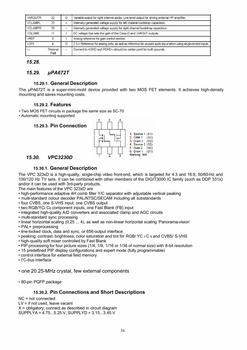
15.29. µPA672T
15.29.1. General Description
The µPA672T is a super-mini-mold device provided with two MOS FET elements. It achieves high-densitymounting and saves mounting costs.
15.29.2. Features
• Two MOS FET circuits in package the same size as SC-70• Automatic mounting supported
15.29.3. Pin Connection
15.30. VPC3230D
15.30.1. General Description
The VPC 323xD is a high-quality, single-chip video front-end, which is targeted for 4:3 and 16:9, 50/60-Hz and100/120 Hz TV sets. It can be combined with other members of the DIGIT3000 IC family (such as DDP 331x)
and/or it can be used with 3rd-party products.The main features of the VPC 323xD are• high-performance adaptive 4H comb filter Y/C separator with adjustable vertical peaking• multi-standard colour decoder PAL/NTSC/SECAM including all substandards• four CVBS, one S-VHS input, one CVBS output• two RGB/YCr Cb component inputs, one Fast Blank (FB) input• integrated high-quality A/D converters and associated clamp and AGC circuits• multi-standard sync processing• linear horizontal scaling (0.25 ... 4), as well as non-linear horizontal scaling ‘Panorama-vision’• PAL+ preprocessing• line-locked clock, data and sync, or 656-output interface• peaking, contrast, brightness, color saturation and tint for RGB/ YC r C b and CVBS/ S-VHS• high-quality soft mixer controlled by Fast Blank
• PIP processing for four picture sizes (1/4, 1/9, 1/16 or 1/36 of normal size) with 8-bit resolution• 15 predefined PIP display configurations and expert mode (fully programmable)• control interface for external field memory• I2C-bus interface
• one 20.25-MHz crystal, few external components
• 80-pin PQFP package
15.30.2. Pin Connections and Short Descriptions
NC = not connectedLV = if not used, leave vacant
X = obligatory; connect as described in circuit diagramSUPPLYA = 4.75...5.25 V, SUPPLYD = 3.15...3.45 V

8/12/2019 Hitachi 42PD6700U Plasma TV
http://slidepdf.com/reader/full/hitachi-42pd6700u-plasma-tv 40/79
35
Pin No.PQFP80-pin
Pin Name Type Connection(if not used)
Short Description
1 B1/CB1IN IN VREF Blue1/Cb1 Analog Component Input
2 G1/Y1IN IN VREF Green1/Y1 Analog Component Input
3 R1/CR1IN IN VREF Read1/Cr1 Analog Component Input
4 B2/CB2IN IN VREF Blue2/Cb2 Analog Component Input
5 G2/Y2IN IN VREF Green2/Y2 Analog Component Input
6 R2/CR2IN IN VREF Read2/Cr2 Analog Component Input
7 ASGF X Analog Shield GNDF8 FFRSTWIN IN LV or GNDD FIFO Reset Write Input
9 VSUPCAP OUT X Digital Decoupling Circuitry Supply Voltage
10 VSUPD SUPPLYD X Supply Voltage, Digital Circuitry
11 GNDD SUPPLYD X Ground, Digital Circuitry
12 GNDCAP OUT X Digital Decoupling Circuitry GND
13 SCL IN/OUT X I2C Bus Clock
14 SDA IN/OUT X I2C Bus Data
15 RESQ IN X Reset Input, Active Low
16 TEST IN GNDD Test Pin, connect to GNDD
17 VGAV IN GNDD VGAV Input
18 YCOEQ IN GNDD Y/C Output Enable Input, Active Low
19 FFIE OUT LV FIFO Input Enable20 FFWE OUT LV FIFO Write Enable
21 FFRSTW OUT LV FIFO Reset Write/Read
22 FFRE OUT LV FIFO Read Enable
23 FFOE OUT LV FIFO Output Enable
24 CLK20 IN/OUT LV Main Clock output 20.25 MHz25 GNDPA OUT X Pad Decoupling Circuitry GND
26 VSUPPA OUT X Pad Decoupling Circuitry Supply Voltage
27 LLC2 OUT LV Double Clock Output
28 LLC1 IN/OUT LV Clock Output
29 VSUPLLC SUPPLYD X Supply Voltage, LLC Circuitry
30 GNDLLC SUPPLYD X Ground, LLC Circuitry
31 Y7 OUT GNDY Picture Bus Luma (MSB)
32 Y6 OUT GNDY Picture Bus Luma
33 Y5 OUT GNDY Picture Bus Luma
34 Y4 OUT GNDY Picture Bus Luma35 GNDY SUPPLYD X Ground, Luma Output Circuitry
36 VSUPY SUPPLYD X Supply Voltage, Luma Output Circuitry
37 Y3 OUT GNDY Picture Bus Luma
38 Y2 OUT GNDY Picture Bus Luma
39 Y1 OUT GNDY Picture Bus Luma
40 Y0 OUT GNDY Picture Bus Luma (LSB)
41 C7 OUT GNDC Picture Bus Chroma (MSB)
42 C6 OUT GNDC Picture Bus Chroma
43 C5 OUT GNDC Picture Bus Chroma
44 C4 OUT GNDC Picture Bus Chroma
45 VSUPC SUPPLYD X Supply Voltage, Chroma Output Circuitry
46 GNDC SUPPLYD X Ground, Chroma Output Circuitry
47 C3 OUT GNDC Picture Bus Chroma
48 C2 OUT GNDC Picture Bus Chroma49 C1 OUT GNDC Picture Bus Chroma
50 C0 OUT GNDC Picture Bus Chroma (LSB)
51 GNDSY SUPPLYD X Ground Sync Pad Circuitry
52 VSUPSY SUPPLYD X Supply Voltage, Sync Pad Circuitry
53 INTLC OUT LV Interlace Output
54 AVO OUT LV Active Video Output
55 FSY/HC/HSYA OUT LV Front Sync/ Horizontal Clamp Pulse/Front-EndHorizontal Sync Output
56 MSY/HS IN/OUT LV Main Sync/Horizontal Sync Pulse
57 VS OUT LV Vertical Sync Pulse
58 FPDAT/VSYA IN/OUT LV Front End/Back-End Data/Front-End Vertical SyncOutput
59 VSTBYY SUPPLYA X Standby Supply Voltage
60 CLK5 OUT LV CCU 5 MHz Clock Output
8/12/2019 Hitachi 42PD6700U Plasma TV
http://slidepdf.com/reader/full/hitachi-42pd6700u-plasma-tv 41/79
76 VSUPAI SUPPLYA X Supply Voltage, Analog Component Inputs Front-End
77 GND AI SUPPLYA X Ground, Analog Component Inputs Front-End
78 VREF OUTPUT X Reference Voltage Top, Analog Component InputsFront-End
79 FB1IN IN VREF Fast Blank Input
80 AISGND SUPPLYA X Signal Ground for Analog Component Inputs, connectto GND AI
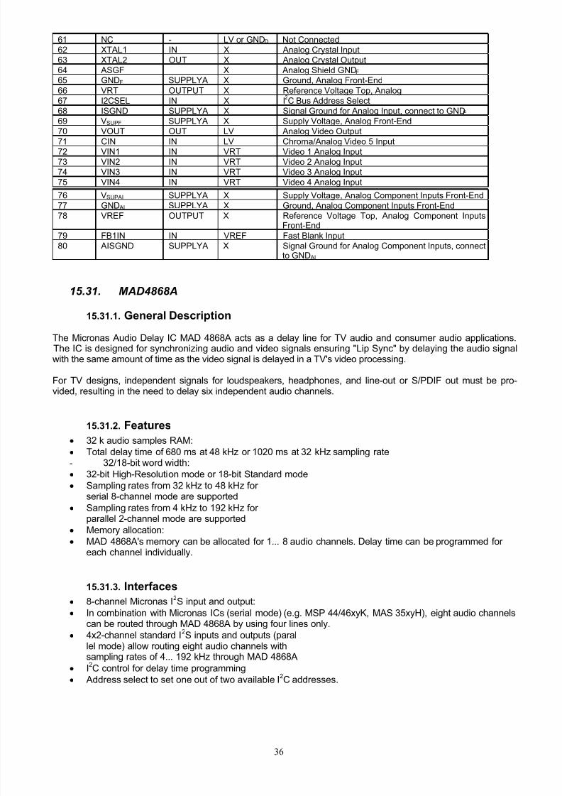
15.31. MAD4868A
15.31.1. General Description
The Micronas Audio Delay IC MAD 4868A acts as a delay line for TV audio and consumer audio applications.The IC is designed for synchronizing audio and video signals ensuring "Lip Sync" by delaying the audio signalwith the same amount of time as the video signal is delayed in a TV's video processing.
For TV designs, independent signals for loudspeakers, headphones, and line-out or S/PDIF out must be pro-vided, resulting in the need to delay six independent audio channels.
15.31.2. Features
32 k audio samples RAM:
Total delay time of 680 ms at 48 kHz or 1020 ms at 32 kHz sampling rate- 32/18-bit word width:
32-bit High-Resolution mode or 18-bit Standard mode
Sampling rates from 32 kHz to 48 kHz forserial 8-channel mode are supported
Sampling rates from 4 kHz to 192 kHz forparallel 2-channel mode are supported
Memory allocation:
MAD 4868A's memory can be allocated for 1... 8 audio channels. Delay time can be programmed foreach channel individually.
15.31.3. Interfaces
8-channel Micronas I2S input and output:
In combination with Micronas ICs (serial mode) (e.g. MSP 44/46xyK, MAS 35xyH), eight audio channelscan be routed through MAD 4868A by using four lines only.
4x2-channel standard I2S inputs and outputs (paral
lel mode) allow routing eight audio channels withsampling rates of 4... 192 kHz through MAD 4868A
I2C control for delay time programming
Address select to set one out of two available I2C addresses.
36
61 NC - LV or GNDD Not Connected
62 XTAL1 IN X Analog Crystal Input
63 XTAL2 OUT X Analog Crystal Output
64 ASGF X Analog Shield GNDF
65 GNDF SUPPLYA X Ground, Analog Front-End
66 VRT OUTPUT X Reference Voltage Top, Analog
67 I2CSEL IN X I2C Bus Address Select
68 ISGND SUPPLYA X Signal Ground for Analog Input, connect to GNDF
69 VSUPF SUPPLYA X Supply Voltage, Analog Front-End
70 VOUT OUT LV Analog Video Output
71 CIN IN LV Chroma/Analog Video 5 Input72 VIN1 IN VRT Video 1 Analog Input
73 VIN2 IN VRT Video 2 Analog Input
74 VIN3 IN VRT Video 3 Analog Input
75 VIN4 IN VRT Video 4 Analog Input

8/12/2019 Hitachi 42PD6700U Plasma TV
http://slidepdf.com/reader/full/hitachi-42pd6700u-plasma-tv 42/79
37
15.31.4. Pinning
15.32. SVP-EX 59B
General Description
To improve the video quality of the PAL CVBS and HD video input, the all layer changed EX59 improve video sharpness
function in HD channel and enhance the 3D PAL quality compared to EX52 Rev. D chips.
16. SERVICE MENU SETTINGSTo enter the service menu, first enter the MENU by pressing “ ” button and then press the digits 4, 7, 2 and 5respectively.

8/12/2019 Hitachi 42PD6700U Plasma TV
http://slidepdf.com/reader/full/hitachi-42pd6700u-plasma-tv 43/79
38
Service Menu Items
16.1. Picture Adjust
Source => All possible sources given with the chasis as a list.
Mode => Three items as a list; NATURAL, DYNAMIC, CINEMA
Colour Temp => Three items as a list; COOL, NORMAL, WARM
Contrast => Slider Bar. Changing value between 0 to 63.
Brightness => Slider Bar. Changing value between 0 to 63.
Sharpness => Slider Bar. Changing value between 0 to 16. Colour => Slider Bar. Changing value between 0 to 99.
R => Slider Bar. Changing value between 0 to 100.
G => Slider Bar. Changing value between 0 to 100.
B => Slider Bar. Changing value between 0 to 100.In this menu preset values for each Mode (Contrast, Brightness, Sharpness, Colour values for each Mode-NATURAL, DYNAMIC, CINEMA) and for each Colour Temp. (R, G, B values for each Colour Temp- COOL,NORMAL, WARM) are determined for each source.
16.2. SOUND1
Menu Subwoofer => If ON, Subwoofer option is available in TV set, and the item is visiblein sound menu, else Subwoofer is not available.
Subwoofer Level (dB) => This value is gain value of Subwoofer output in dB. -30...12
Subwoofer Corner Freq. (x10Hz) => Last low frequency value that is amplified. 5...40
Menu Dolby Prologic => No functionality now.
Menu Equalizer => If ON, visible in sound menu, else invisible.
Menu Lineout => No functionality now.
Menu Headphone => If ON, visible in sound menu, else invisible.
Menu Hyper Sound => If ON, visible in sound menu, else invisible.
Menu Wide Sound => If ON, visible in sound menu, else invisible.
Menu Dynamic Bass => If ON, visible in sound menu, else invisible.
Menu Virtual Dolby => If ON, visible in sound menu, else invisible.
Carrier Mute => If ON, in the absence of an FM carrier the output is muted, else not.
Virtual Dolby Text => Active if VIRTUAL DOLBY is ON. According to the selection; seen insound menu as 3D PANORAMA or VIRTUAL DOLBY.
16.3. SOUND 2
AVL => AVL is controlled from this menu by service user. ON/OFF
Menu AVL => If ON, AVL item is visible in sound menu, and AVL can be controlled fromsound menu by normal user, else AVL is invisible to normal user.
FM PRESCALE AVL ON => If AVL ON, set value in this item is used as prescale valuefor the related standard. 0...127
NICAM PRESCALE AVL ON => If AVL ON, set value in this item is used as prescale valuefor the related standard. 0...127
SCART PRESCALE AVL ON => If AVL ON, set value in this item is used as prescale valuefor scart outputs. 0...127
SCART VOLUME AVL ON => If AVL ON, set value in this item is used as volume value for
scart1 and scart2. 0...127 FM PRESCALE AVL OFF => If AVL OFF, set value in this item is used as prescale value
for the related standard. 0...127
NICAM PRESCALE AVL OFF => If AVL OFF, set value in this item is used as prescale valuefor the related standard. 0...127
SCART PRESCALE AVL OFF => If AVL OFF, set value in this item is used as prescale valuefor scart outputs. 0...127
SCART VOLOUME AVL OFF => If AVL OFF, set value in this item is used as volume value forscart1 and scart2. 0...127
16.4. Options
Screen Saver =>
FIRST APS => If ON, first APS menu is opened when the TV opened with thefactory default settings.

8/12/2019 Hitachi 42PD6700U Plasma TV
http://slidepdf.com/reader/full/hitachi-42pd6700u-plasma-tv 44/79
39
APS VOLUME => After First APS function finishes, the volume of the TV is that value.
AGC => Tuner AGC value.
Factory Reset => OK to activate. When OK pressed on this item, factory defaultsloaded.
Enter Flash Mode =>TV Norm
BG => If ON, supported, else not supported
DK => If ON, supported, else not supported.
I => If ON, supported, else not supported.
L => If ON, supported, else not supported. LP => If ON, supported, else not supported.
M => If ON, supported, else not supported. Features
PIP/PAP => If ON, PIP/PAP available else not.
Blue Background => If ON, Blue Background is visible in Features Menu else not.
Menu Transparency => If ON, Menu Transparency is visible in Features Menu else not.
Menu Timeout => If ON, Menu Timeout is visible in Features Menu else not.
Backlight => If ON, Backlight is visible in Features Menu else not.
Single Tuner =>Teletext
Teletext Language => Teletext Language may be controlled from this menu by service
user. Menu Teletext Language => If ON, Teletext Language item is visible in Features Menu, and
Teletext Language can be controlled from Features Menu by normal user, else Teletext Language isinvisible to normal user.
Source
TV
SC1
SC2
SC2 SVHS
SC3
SC3 SVHS
YPBPR
FAV
SVHS
HDMI
PC
This menu is related with the options of the chassis. These items may be ON or OFF. If ON, the source is
available in TV set, and the item is visible in source menu, else the source may be available but invisible to user.
17. IC DESCRIPTIONS (FOR DIGITAL)
STI5518 24C32
MAX232_SMD STV0360
74HCU04 MAX809TSH22 TDCC2345TV39A
CS4334 STV0700
AMIC A43L2616
MX29LV160T
17.1. STI5518
17.1.1. General Description
The STi5518 is a highly integrated single-chip decoder, designed for use in feature-rich mass-market set-top boxes. Itintegrates a high-performance 32-bit CPU, a dedicated block for DVB/DirecTV transport demultiplexing and descrambling,
modules for MPEG-2 video and audio decoding with 3D-surround and MP3 support, advanced display and graphicsfeatures, a digital video encoder and all of the system peripherals required in a typical low-cost interactive receiver.
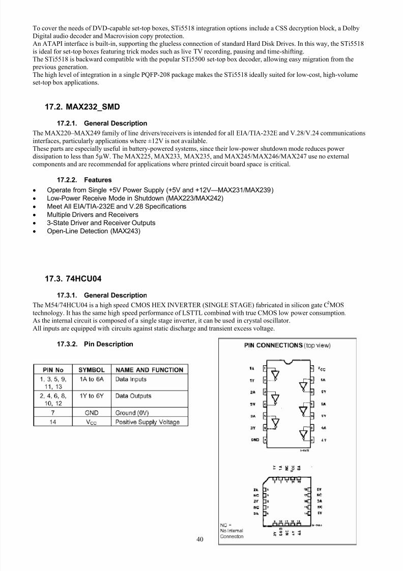
8/12/2019 Hitachi 42PD6700U Plasma TV
http://slidepdf.com/reader/full/hitachi-42pd6700u-plasma-tv 45/79
40
To cover the needs of DVD-capable set-top boxes, STi5518 integration options include a CSS decryption block, a DolbyDigital audio decoder and Macrovision copy protection.An ATAPI interface is built-in, supporting the glueless connection of standard Hard Disk Drives. In this way, the STi5518
is ideal for set-top boxes featuring trick modes such as live TV recording, pausing and time-shifting.The STi5518 is backward compatible with the popular STi5500 set-top box decoder, allowing easy migration from the previous generation.The high level of integration in a single PQFP-208 package makes the STi5518 ideally suited for low-cost, high-volumeset-top box applications.
17.2. MAX232_SMD
17.2.1. General Description
The MAX220–MAX249 family of line drivers/receivers is intended for all EIA/TIA-232E and V.28/V.24 communications
interfaces, particularly applications where ±12V is not available.These parts are especially useful in battery-powered systems, since their low-power shutdown mode reduces powerdissipation to less than 5µW. The MAX225, MAX233, MAX235, and MAX245/MAX246/MAX247 use no externalcomponents and are recommended for applications where printed circuit board space is critical.
17.2.2. Features
Operate from Single +5V Power Supply (+5V and +12V—MAX231/MAX239)
Low-Power Receive Mode in Shutdown (MAX223/MAX242) Meet All EIA/TIA-232E and V.28 Specifications
Multiple Drivers and Receivers
3-State Driver and Receiver Outputs
Open-Line Detection (MAX243)
17.3. 74HCU04
17.3.1. General Description
The M54/74HCU04 is a high speed CMOS HEX INVERTER (SINGLE STAGE) fabricated in silicon gate C2MOS
technology. It has the same high speed performance of LSTTL combined with true CMOS low power consumption.As the internal circuit is composed of a single stage inverter, it can be used in crystal oscillator.
All inputs are equipped with circuits against static discharge and transient excess voltage.
17.3.2. Pin Description

8/12/2019 Hitachi 42PD6700U Plasma TV
http://slidepdf.com/reader/full/hitachi-42pd6700u-plasma-tv 46/79
41
17.4. TSH22
17.4.1. General Description
The TSH22 is a dual bipolar operational amplifier offering a single supply operation from 3V to 30V with very good performances: medium speed (25MHz), unity gain stability and low noise.The TSH 22 is therefore an enhanced replacement of standard dual operational amplifiers.
17.4.2. Pin Connections
17.5. CS4334
17.5.1. General Description
The CS4334 family members are complete, stereo digital-to-analogue output systems including interpolation, 1-bit D/Aconversion and output analogue filtering in an 8-pin package. The CS4334/5/6/7/8/9 support all major audio data interfaceformats and the individual devices differ only in the supported interface format.
The CS4334 family is based on delta-sigma modulation, where the modulator output controls the reference voltage input toan ultra-linear analogue low-pass filter. This architecture allows for infinite adjustment of sample rate between 2 kHz and100 kHz simply by changing the master clock frequency.The CS4334 family contains on-chip digital de-emphasis, operates from a single +5V power supply, and requires minimalsupport circuitry. These features are ideal for portable CD players and other portable playback systems.
17.5.2. Features
Complete Stereo DAC System: Interpolation, D/A, Output Analogue Filtering
24-Bit Conversion
96 dB Dynamic Range
Low Distortion
Low Clock Jitter Sensitivity
Single 5 V Power Supply
Filtered Line Level Outputs
On-Chip Digital De-emphasis
Soft Ramp to Quiescent Output Voltage
Functionally Compatible with CS4330/31/33
17.6. AMIC A43L2616
17.6.1. General Description
The A43L2616-PH is 67,108,864 bits synchronous high data rate Dynamic RAM organized as 4 X 1,048,576words by 16 bits, fabricated with AMIC’s high performance CMOS technology. Synchronous design allowsprecise cycle control with the use of system clock. I/O transactions are possible on every clock cycle. Range ofoperating frequencies, programmable latencies allows the same device to be useful for a variety of highbandwidth, high performance memory system applications.
17.6.2. Features
JEDEC standard 3.3V power supply
LVTTL compatible with multiplexed address Four banks / Pulse RAS
MRS cycle with address key programs

8/12/2019 Hitachi 42PD6700U Plasma TV
http://slidepdf.com/reader/full/hitachi-42pd6700u-plasma-tv 47/79
42
All inputs are sampled at the positive going edge of the system clock
Clock Frequency: 166MHz @ CL=3143MHz @ CL=3
Burst Read Single-bit Write operation
DQM for masking
Auto & self refresh
64ms refresh period (4K cycle)
54 Pin TSOP (II)
17.6.3. Pin Description

8/12/2019 Hitachi 42PD6700U Plasma TV
http://slidepdf.com/reader/full/hitachi-42pd6700u-plasma-tv 48/79
17.7. MX29LV160T
17.7.1. General Description
The MX29LV160T/B & MX29LV160AT/AB is a 16-megabit Flash memory organized as 2M bytes of 8 bits or 1M wordsof 16 bits. MXIC's Flash memories offer the most cost-effective and reliable read/write non-volatile random accessmemory. The MX29LV160T/B & MX29LV160AT/AB is packaged in 44-pin SOP, 48-pin TSOP and 48-ball CSP. It isdesigned to be reprogrammed and erased in system or in standard EPROM programmers.
The standard MX29LV160T/B & MX29LV160AT/AB offers access time as fast as 70ns, allowing operation of high-speedmicroprocessors without wait states. To eliminate bus contention, the MX29LV160T/B &MX29LV160AT/AB has separatechip enable (CE) and output enable (OE) controls.
MXIC's Flash memories augment EPROM functionality with in-circuit electrical erasure and programming. TheMX29LV160T/B & MX29LV160AT/AB uses a command register to manage this functionality. The command registerallows for 100% TTL level control inputs and fixed power supply levels during erase and programming, while maintainingmaximum EPROM compatibility.MXIC Flash technology reliably stores memory contents even after 100,000 erase and program cycles. The MXIC cell isdesigned to optimize the erase and programming mechanisms. In addition, the combination of advanced tunnel oxide processing and low internal electric fields for erase and program operations produces reliable cycling. The
MX29LV160T/B & MX29LV160AT/AB uses a 2.7V~3.6V VCC supply to perform the High Reliability Erase and autoProgram/Erase algorithms.The highest degree of latch-up protection is achieved with MXIC's proprietary non-epi process. Latch-up protection is
proved for stresses up to 100 milliamps on address and data pin from -1V to VCC + 1V.
17.7.2. Features
Extended single - supply voltage range 2.7V to 3.6V
2,097,152 x 8/1,048,576 x 16 switchable
Single power supply operation
Fast access time: 70/90ns
Low power consumption
Command register architecture
Auto Erase (chip & sector) and Auto Program
Erase Suspend/Erase Resume
Status Reply
Ready/Busy pin (RY/BY) Sector protection
CFI (Common Flash Interface) compliant (for MX29LV160AT/AB)
100,000 minimum erase/program cycles
Latch-up protected to 100mA from -1V to VCC+1V
Boot Sector Architecture
Low VCC write inhibit is equal to or less than 1.4V
Compatibility with JEDEC standard
17.7.3. Pin Description
43

8/12/2019 Hitachi 42PD6700U Plasma TV
http://slidepdf.com/reader/full/hitachi-42pd6700u-plasma-tv 49/79
17.8. 24C32
17.8.1. General Description
The AT24C32/64 provides 32,768/65,536 bits of serial electrically erasable and programmable read onlymemory (EEPROM) organized as 4096/8192 words of 8 bits each. The device’s cascadable feature allows up to8 devices to share a common 2-wire bus. The device is optimized for use in many industrial and commercialapplications where low power and low voltage operation are essential. The AT24C32/64 is available in spacesaving 8-pin JEDEC PDIP, 8-pin JEDEC SOIC, 8-pin EIAJ SOIC, and 8-pin TSSOP (AT24C64) packages and is
accessed via a 2-wire serial interface. In addition, the entire family is available in 2.7V (2.7V to 5.5V) and 1.8V(1.8V to 5.5V) versions.
17.8.2. Features
Low-Voltage and Standard-Voltage Operation
Low-Power Devices (ISB= 2 µA at 5.5V) Available
Internally Organized 4096 x 8, 8192 x 8
2-Wire Serial Interface
Schmitt Trigger, Filtered Inputs for Noise Suppression
Bidirectional Data Transfer Protocol
100 kHz (1.8V, 2.5V, 2.7V) and 400 kHz (5V) Clock Rate
Write Protect Pin for Hardware Data Protection
32-Byte Page Write Mode (Partial Page Writes Allowed) Self-Timed Write Cycle (10 ms max)
High Reliability
Automotive Grade and Extended Temperature Devices Available
8-Pin JEDEC PDIP, 8-Pin JEDEC SOIC, 8-Pin EIAJ SOIC, and 8-pin TSSOP Packages
17.8.3. Pin Description
SERIAL CLOCK (SCL): The SCL input is used to positive edge clock data into each EEPROM device and negative edgeclock data out of each device.
SERIAL DATA (SDA): The SDA pin is bidirectional for serial data transfer. This pin is open-drain driven and may bewire-ORed with any number of other open-drain or open collector devices.DEVICE/PAGE ADDRESSES (A2, A1, A0): The A2, A1 and A0 pins are device address inputs that are hard wired or leftnot connected for hardware compatibility with AT24C16. When the pins are hardwired, as many as eight 32K/64K devicesmay be addressed on a single bus system (device addressing is discussed in detail under the Device Addressing section).When the pins are not hardwired, the default A2, A1, and A0 are zero.WRITE PROTECT (WP): The write protect input, when tied to GND, allows normal write operations. When WP is tied
high to VCC, all write operations to the upper quadrant (8/16K bits) of memory are inhibited. If left unconnected, WP isinternally pulled down to GND.
44

8/12/2019 Hitachi 42PD6700U Plasma TV
http://slidepdf.com/reader/full/hitachi-42pd6700u-plasma-tv 50/79
45
17.9. STV0360
17.9.1. General Description
The STV0360 is a single-chip COFDM (coded orthogonal frequency division multiplex) demodulator that performs IF toMPEG-2 block processing of OFDM carriers. It is intended for digital terrestrial receivers for compressed video, sound anddata services.
The chip implements all the functions from the tuner IF output up to the MPEG-2 transport stream input.The STV0360 is fully compliant with the DVB-T specification (ETS 300 744) and handles 2K/8K modes.The STV0360 integrates an A/D converter that delivers the required performance to handle up to 64 QAM carriers in adirect IF sampling architecture, thus eliminating the need for an external down-converter. The chip also integrates aninternal programmable gain amplifier (PGA) to compensate for SAW filter level degradation, thus eliminating the need forexternal IF amplifiers. A 10-bit ADC, intended for RF signal strength indication, eliminates the need for externalcomponents when using wide-band AGC tuners.
In addition to all the demodulation and FEC (forward error correction) functions required for recovery of the QAMmodulated bit streams with very low BER, it also includes several features that give easy and immediate access to various
quality monitoring parameters or lock status. The STV0360 also provides output such as delayed AGC or noise-free I²C bus
dedicated to tuner control, which facilitates the design of high quality integrated receiver decoders.The STV0360 outputs error-corrected MPEG-2 transport streams and complies with the DVB common interface format,with programmable data clock frequency. It also interfaces seamlessly with the packet de-multiplexers embedded in theSTi55xx Omega family of single-chip decoders.
17.9.2. Features
Decodes DVB-T (ETS300744) and NorDig II
TPS decoded or automatic FEC mode detection
Embeds PGA for IF level adaptation
Generates system clock on-chip from 20 to 27-MHz crystal quartz
Four I²C addresses available
Low power consumption (< 500 mW)
Small footprint: TQFP64 (10 X 10 mm)
1.8 V operation, CMOS technology
17.9.3. Pin Description

8/12/2019 Hitachi 42PD6700U Plasma TV
http://slidepdf.com/reader/full/hitachi-42pd6700u-plasma-tv 51/79
46

8/12/2019 Hitachi 42PD6700U Plasma TV
http://slidepdf.com/reader/full/hitachi-42pd6700u-plasma-tv 52/79
47
17.10. MAX809
17.10.1. General DescriptionThe MAX803/MAX809/MAX810 are microprocessor (µP) supervisory circuits used to monitor the power supplies in µPand digital systems. They provide excellent circuit reliability and low cost by eliminating external components andadjustments when used with +5V, +3.3V,+3.0V, or +2.5V powered circuits. These circuits perform a single function: theyassert a reset signal whenever the VCC supply voltage declines below a preset threshold, keeping it asserted for at least140ms after VCC has risen above the reset threshold. Reset thresholds suitable for operation with a variety of supply
voltages are available. The MAX803 has an open-drain output stage, while the MAX809/MAX810 have push-pull outputs.The MAX803’s open-drain RESET output requires a pull-up resistor that can be connected to a voltage higher than VCC.The MAX803/MAX809 have an active-low RESET output, while the MAX810 has an active-high RESET output. Thereset comparator is designed to ignore fast transients on VCC, and the outputs are guaranteed to be in the correct logic state
for VCC down to 1V. Low supply current makes the MAX803/MAX809/MAX810 ideal for use in portable equipment. TheMAX803 is available in a 3-pin SC70 package, and the MAX809/MAX810 are available in 3-pin SC70 or SOT23
packages.
17.10.2. Features
1 Precision M onitorin g of +2.5V, +3V, +3.3V, and +5V Power-Suppl y Voltages
Fully Specifie d Over Tem peratu re
Available in T hree Output Config uratio nsOpen-Drain RESET Output (MAX803)Push-Pull RESET Output (MAX809)Push-Pull RESET Output (MAX810)
140ms min Pow er-On Reset Pulse Wid th
12µA Supply Current
Guarantee d Reset Valid to VCC= +1V
Power Suppl y Transi ent Immunity No External Components
3-Pin SC70 and SOT23 Package s

8/12/2019 Hitachi 42PD6700U Plasma TV
http://slidepdf.com/reader/full/hitachi-42pd6700u-plasma-tv 53/79
17.10.3. Pin Description
17.11. TDCC2345TV39A
17.11.1. General Description
Receiving System : Designed to cover all bands in VHF and UHF including digital terrestrial channels for DVB-Tsystem.
Receiving Channel : 47 MHz ~ 862 MHz
Intermediate Frequency : Digital (center) 36.125 MHz
Input Impedance : 75, Unbalanced.
IF Output Impedance : 75, Balanced.
Loop through RF output Impedance : 75, Unbalanced.
Band Change-Over System : PLL system
Tuning System : PLL system
Pin-out for the port to control the switchable saw
17.11.2. Pin Description
48

8/12/2019 Hitachi 42PD6700U Plasma TV
http://slidepdf.com/reader/full/hitachi-42pd6700u-plasma-tv 54/79
17.12. STV0700
17.12.1. General description
The STV0700 controller contributes to offer an optimized, homogeneous and complete solution for digital TV receiver and
Set Top Box manufacturers that want to quickly implement the Common Interface. The STV0700 includes the necessaryI/Os to interface to the MPEG Transport stream generated by the receiver demodulator and daisy chain it through twoindependent Common Interface modules and back to the demultiplexer. The STV0700 interfaces with major digital TVreceiver microprocessors. An I2C bus is used for initialization and module selection, while a Universal Control Signal
Generator (UCSG) maps CPU control bus into Command Interface control signals. To minimize pin count, host address anddata buses transit through external buffers that are driven by the STV0700. The STV0700 includes a memory mode that
allows the use any of the Common Interface slots to read and write an 8-bit PC Card Memory card. This feature gives thereceiver memory extension capability for software upgrade or better performance.
17.12.2. Features
Module Interface
2 independent module capability
Common Interface Standard compliant
o DVB_CI (CENELEC EN-50221)
o NRSS-B (SCTE IS-679 Part B)
o DAVIC v1.2 (CA0 interface)
Memory PCMCIA compliance (R2)o 8-bit data access
o 26-bit address Memory Card
Attribute Memory access (CIS, Tupple)
High speed capability
o Up to 20Mbits/s on Command Interfaceo Up to 100Mbits/s on Transport Stream
Polling and Interrupt modes
Hot Insertion (Automatic and Reset VCC handling)
3.3V (5V tolerant) I/O buffers
IEEE 1149.1 Boundary Scan Compliant
Test Access Port
LSI 64008, TC81220F IDTR3041
I2C port
o STV0700 Set-upo Slot selection
o Cascade mode management (up to 4STV0700)
Chip Select bank and Interrupt facilities
3.3V (5V tolerant) I/O buffers
Digital Video Stream Interface
Host microprocessor Interface
Universal Control Signal Generator(UCSG)o PC Card control signals generation
o Supports PowerPC, ARM, ST20,68xxx, TMS,
MPEG II Transport Stream compliant
with FEC and DEMUX ICs
17.12.3. Pin Description
(serial/parallel configurable interface)
3.3V (5V tolerant) I/O buffer for direct interface
49

8/12/2019 Hitachi 42PD6700U Plasma TV
http://slidepdf.com/reader/full/hitachi-42pd6700u-plasma-tv 55/79
50

8/12/2019 Hitachi 42PD6700U Plasma TV
http://slidepdf.com/reader/full/hitachi-42pd6700u-plasma-tv 56/79
51

8/12/2019 Hitachi 42PD6700U Plasma TV
http://slidepdf.com/reader/full/hitachi-42pd6700u-plasma-tv 57/79
52

8/12/2019 Hitachi 42PD6700U Plasma TV
http://slidepdf.com/reader/full/hitachi-42pd6700u-plasma-tv 58/79

8/12/2019 Hitachi 42PD6700U Plasma TV
http://slidepdf.com/reader/full/hitachi-42pd6700u-plasma-tv 59/79
SM012 BLOCK DIAGRAM
MAIN BOARD
MAIN_L, MAIN_R
AUDIO
AMPLIFIER
D-CLASS
AUDIO AMP BOARD
LVDS OUT
SDA5550
MCU
MICRONAS
PSU
SVP-EX59
AUDIO
DECODING
MSP3411G
MICRONAS
IDTV, SVHS,MMC(RGB), PC IN
VPC3230D
VIDEO PROCESSOR
PIP PICTURE
MICRONAS
8-BIT YUV
24-BIT RGBHDMI DECODER
SIL9993
A U D I O /
V I D E O /
G R A P H I C S
I N /
O U T
19. APPENDIX B
19.1. BLOCK DIAGRAM
54

8/12/2019 Hitachi 42PD6700U Plasma TV
http://slidepdf.com/reader/full/hitachi-42pd6700u-plasma-tv 60/79
SM012 POWER BOARD - SHEET 1
19.1. SCHEMATIC DIAGRAMS
55

8/12/2019 Hitachi 42PD6700U Plasma TV
http://slidepdf.com/reader/full/hitachi-42pd6700u-plasma-tv 61/79
SM012 POWER BOARD - SHEET 2
56

8/12/2019 Hitachi 42PD6700U Plasma TV
http://slidepdf.com/reader/full/hitachi-42pd6700u-plasma-tv 62/79
SM012 POWER BOARD - SHEET 3
57

8/12/2019 Hitachi 42PD6700U Plasma TV
http://slidepdf.com/reader/full/hitachi-42pd6700u-plasma-tv 63/79
SM012 POWER BOARD - SHEET 4
58

8/12/2019 Hitachi 42PD6700U Plasma TV
http://slidepdf.com/reader/full/hitachi-42pd6700u-plasma-tv 64/79
SM012 POWER BOARD - SHEET 5
59

8/12/2019 Hitachi 42PD6700U Plasma TV
http://slidepdf.com/reader/full/hitachi-42pd6700u-plasma-tv 65/79

8/12/2019 Hitachi 42PD6700U Plasma TV
http://slidepdf.com/reader/full/hitachi-42pd6700u-plasma-tv 66/79

8/12/2019 Hitachi 42PD6700U Plasma TV
http://slidepdf.com/reader/full/hitachi-42pd6700u-plasma-tv 67/79
SM012 MAIN BOARD - VPC3230 CIRCUIT
16V220n
C326
20.25MHz
X300
5 0 V
1 0 u
C 3 3 1
S D A 3
75R
R311
16V
100n
C336 R X 1_
R S T #
5 0 V
3 3 0 p
C 3 0 9
2 5 V
4 7 n
C 3 0 6
50V
270p
C334
VCCD2 _3V3
5 0 V
3 3 0 p
C 3 0 8
5 0 V
3 3 0 p
C 3 1 0
50V
1n5
C319
MMC _G
1 0 0 R
R 3 2 0
5 0 V
3 p 3
C 3 3 0
16V220n
C324
16V100n
C344
5 0 V
1 n 5
C 3 4 5
2 2 R
R 3 1 7
16V
220n
C329
5 0 V
1 0 u
C 3 1 6
50V10u
C317
CLK_2EX
50V
68n
C343
50V
390p
C320
16V
220n
C328
VCCD2 _3V3
2 5 V
2 n 2
C 3 3 3
75R
R307
16V
220n
C339
75R
R309
2 2 R
R 3 1 6
75R
R305
VCCD2 _3V3
50V
390p
C337
C I N
25V
47n
C323
50V
330p
C313
MMC _R
V x
t o V P C
25V
560p
C335
S C L 3
1 0 0 R
R 3 1 8
STBY _5V
2 5 V
4 7 n
C 3 4 7
VCCD2 _3V3
75R
R304
1 6 V
1 0 0 n
C 3 4 6
DVS _2EX
VCC _5V
VCC _5V
50V
1n5
C338
75R
R310
50V
1n5
C341
MMC _B
16V
220n
C318
16V
220n
C327
1 0 0 R
R 3 1 9
25V
47n
C340
1n
C321
V C C D 2_
3 V 3
16V220n
C325
D H S_
2 E X
5 0 V
3 p 3
C 3 3 2
R1
R2
R3
R4
33R R322
18
2
3
4
7
6
5
R1
R2
R3
R4
33R R323
18
2
3
4
7
6
5
1 0 k
R 3 1 5
VCC _5V
5 0 V
3 9 0 p
C 3 0 5
VPC323XD
IC216
1
B 1 / C
B 1 I N
2
G 1 / Y
1 I N
3
R 1 / C
R 1 I N
4
B 2 / C
B 2 I N
5
G 2 / Y
2 I N
6
R 2 / C
R 2 I N
7
A S G F
1
8
N C 1
9
V S U P C A P
1 0
V S U P D
1 1
G N D D
1 2
G N D C A P
1 3
S C L
1 4
S D A
1 5
R E
S Q
1 6
T E
S T
25GNDPA
26VSUPPA
27LLC2
28LLC1
29VSUPLLC
30GNDLLC
31Y7
32Y6
33Y5
34Y4
35GNDY
36VSUPY
37Y3
38Y2
39Y1
40Y0
4 9
C 1
5 0
C 0
5 1
G N D S Y
5 2
V S U P S Y
5 3
I N T L
C
5 4
A V
O
5 5
F S Y / H
C
5 6
M S Y / H
S
5 7
V S
5 8
F P D A T
5 9
V S T B Y
6 0
C L K
5
6 1
N C 2
6 2
X T A L
1
6 3
X T A L
2
6 4
A S G F
2
65 GNDF
66 VRT
67 I 2CSEL
68 ISGND
69 VSUPF
70 V OUT
71 CIN
72 VINI
73 VIN2
74 VIN3
75 VIN4
76 VSUPAI
77 GNDAI
78 VR EF
79 FB1IN
80 A ISGND
1 7
V G A V
1 8
Y C O E Q
1 9
F F I E
2 0
F F
W E
4 5
V S U P C
4 6
G N D C
4 7
C 3
4 8
C 2
2 1
F F
R S T W
2 2
F F
R E
2 3
F F
O E
2 4
C L K
2 0
22R
R321
VCCD _3V3S303
VCCD2 _3V3
75R
R300
16V220n
C342
S301
BLM21B201S
L308
L300
B
L M 2 1 B 2 0 1 S
L 3 1 2
BLM21B201S
L315
B L M 2 1 B 2 0 1 S
L 3 1 4
B L M 2 1 B 2 0 1 S
L 3 1 3
B L M 2 1 B 2 0 1 S
L 3 1 1
S 3 0 2
1 6 V
2 2 0 n
C 3 4 8
5 0 V
1 n 8
C 3 4 9
1 6 V
1 0 0 u
C 3 5 0
PI5V330_SOIC
IC317
1A
3C
5E
7G 10J
12L
14N
16R
2B
4D
6F
8H
15O
13M
9I
11K
PI5V330_SOIC
IC318
1A
3C
5E
7G 10J
12L
14N
16R
2B
4D
6F
8H
15O
13M
9I
11K
1k
R325
1k
R326
RGB _SW1
RGB _SW2
SC1 _R
SC2 _R
SC1 _G
SC2 _G
VCC _5V
VCC _5V
SC1 _B
RGB _R IN
SC2 _B
1 6 V
1 0 0 n
C 3 5 2
1 0 0 n
C353
RCA _PB
RCA _PR
RCA _Y
RGB _GIN
RGB _BIN
SC1 _FB
FB
S307
S308
S309
S310
S311
S312
S314
SC2 _FB
680n
C322
75R
R306
MAD4868A
IC2001
1 2
N C 1 2
1 3
I 2 S_
D E L_
O U T 2
1 4
I 2 S_
D E L_
O U T 3
1 5
I 2 S_
D E L_
O U T 4
1 6
D V
S U P 2
1 7
D V
S S 2
1 8
I 2 S_
D E L_ I N
2
1 9
I 2 S_
D E L_ I N
3
2 0
I 2 S_
D E L_ I N
4
2 1
N C 1 3
2 2
N C 1 4
23NC15
24NC16
25NC17
26NC18
27NC19
28NC20
29NC21
30NC22
31NC23
32NC24
33NC25
3 4
R E
S E
T Q
3 5
T E
S T
3 6
D V
S S 1
3 7
D V
S U P 1
3 8
I 2 S_
D E L_
W S
3 9
I 2 S_
D E L_
C L
4 0
I 2 S_
D E L_ I N
1
4 1
I 2 S_
D E L_
O U T 1
4 2
A D R_
S E L
4 3
S D A
4 4
S C L
1 N C 1
2 N C 2
3 N C 3
4 N C 4
5 N C 5
6 N C 6
7 NC7
8 N C 8
9 N C 9
10 NC1 0
11 NC11
SCL SDA
R 1
R 2
R 3
R 4
1 0 R
R 2 0 2 8
1 8
2 3 4
7 6 5
1 0 0 R
R 2 0 2 6
1 0 0 R
R 2 0 2 7
I 2 S_
D A_ I N 1
I 2 S_
D A_
O U T
I 2 S_
C L
I 2 S_
W S
50V10n
C2047
25V100n
C2048
50V10u
C2046
R E S E T Q_
M S P
VCC _5V
B L M 2 1 B 2 0 1 S
L 2 0 0 9
RGB _B _VPC
RGB _G _VPC
RGB _R _VPC
S316
FB _VPC
V C C_
5 V 5
0 V 2
2 0 p
C 3 5 7
7 5 R
R 3 3 2
A
W H I T E_ F A V
J K 3 0 0
1 2 3
R C A_
Y
A
W H I T E_ F A V
J K 3 0 1
1 2 3
7 5 R
R 3 3 3
5 0 V 2
2 0 p
C 3 5 6
5 0 V 2
2 0 p
C 3 5 8
R C A_
P R
R C A_
P B
BAV99
D104
7 5 R
R 3 3 1
BAV99
D102
BAV99
D106
A
L AUDIO FAV
JK303
123
A
R AUDIO FAV
JK304
123
B L M 2 1 A 6 0 1 S
L 3 1 6
5 0 V
4 7 0 p
C 3 5 9
B L M 2 1 A 6 0 1 S
L 3 1 7
5 0 V
4 7 0 p
C 3 6 0
Y P B P R_
A U D I O_ L_ I N
Y P B P R_
A U D I O_
R_ I N
A
1 P_
R E D_ F A V
J K 3 0 2
1 2 3
AUDIO _R _LINE_OUT
AUDIO _L_LINE_OUT
A U D I O_ L_ L I N E_
O U T
A U D I O_
R_ L I N E_
O U T
S 3 2 3
S 3 2 4
S325
S326
S 3 3 0
S 3 3 1
B Z T 5 5 C 1 0
D 2 2 5
A1
K 2
B Z T 5 5 C 1 0
D 2 2 6
A1
K 2
PL301
1
2
3
4 SUBW
RGB _G _VPC
RGB _R _VPC
RGB _B _VPC
FB _VPC
1 0 k
R 2 0 2 9
1n
C361
S V H S f r o m S C 2_
C
PI5V330_SOIC
IC316
1A
3C
5E
7G 10J
12L
14N
16R
2B
4D
6F
8H
15O
13M
9I
11K
VCC _5V
1 0 0 n
C362
SC1 _R
1k
R2030RGB _SW3
SC1 _G
SC2 _R
SC2 _G
SC2 _B
SC1 _B
SC2 _FB
SC1 _FB
S 3 4 0
33R
R2031
33R
R2032BLM21B201S
L2010
BLM21B201S
L2011
220n C363
220n C364
220n C365
S 3 3 7
S 3 3 6
VGA _GIN
VGA _R IN
VGA _BIN
R IN2
GIN2
BIN2
50V
330p
C312
50V
330p
C311
4 k
R 3 1 2
1 k
R 3 1 3
V C C_
5 V
DIN[6]
DIN[2]
D I N [ 0 - 2
3 ]
DIN[1]
DIN[5]
DIN[4]
DIN[0]
DIN[7]
DIN[3]
M M C R G B I N P U T S
S C A R T R G B
N.C
N.C
b u c a p l e r i n y e r i n e t e k 1 0 0 n f t a k a b i l i r s i n .
N.C
N.C
N.C
N.C
SVP ENTEGR ESINE
P b
BA CK
RI GHT
BA CK
L E F T
RGB SWITCHING FOR SVP
RGB SWITCHING FOR VPC
3 0 0 3 2 2 3 3
Y
3 0 0 3 2 2 3 4
P r
VGA& YPbPr SWITCHING
N.C
N.C
62

8/12/2019 Hitachi 42PD6700U Plasma TV
http://slidepdf.com/reader/full/hitachi-42pd6700u-plasma-tv 68/79

8/12/2019 Hitachi 42PD6700U Plasma TV
http://slidepdf.com/reader/full/hitachi-42pd6700u-plasma-tv 69/79
SM012 MAIN BOARD - DDR RAM CIRCUIT
EM6A9320IC1
81VSSQ_G9
1 7
D Q 1_
B 5
6
D Q 0_
A 6
4 6
V D D_
D 1 0
88VSSQ_H4
5
D Q 2_
A 5
4
D Q 3_
A 4
1 3
D Q 4_
B 1
2 6
D Q 5_
C 2
2 5
D Q 6_
C 1
3 7
D Q 7_
D 1
5 0
D Q 1 6_ E 2
4 9
D Q 1 7_ E 1
6 2
D Q 1 8_ F 2
6 1
D Q 1 9_ F 1
8 6
D Q 2 0_ H 2
8 5
D Q 2 1_ H 1
9 7
D Q 2 2_ J 1
9 8
D Q 2 3_ J 2
2
D M 0_
A 2
7 4
D M 2_
G 2
1
D Q S 0_
A 1
7 3
D Q S 2_
G 1
1 3
2 N C_ L 1 2
3
V S S Q_
A 3
1 0
V S S Q_
A 1 0
2 7
V S S Q_
C 3
2 8
V S S Q_
C 4
2 9
V S S Q_
C 5
3 2
V S S Q_
C 8
3 3
V S S Q_
C 9
3 4
V S S Q_
C 1 0
4 1
V S S Q_
D 5
4 4
V S S Q_
D 8
5 2
V S S Q_ E 4
5 7
V S S Q_ E 9
6 4
V S S Q_ F 4
6 9
V S S Q_ F 9
7 6
V S S Q_
G 4
100VSSQ_J4
93VSSQ_H9
105VSQ_J9
112VSS _K4
117VSS _K9
101VSS _J5
102VSS _J6
103VSS _J7
104VSS _J8
40VSS _D4
42VSS _D6
43VSS _D7
45VSS _D9
53VSS _E5
54VSS _E6
55VSS _E7
56VSS _E8
65VSS _F5
66VSS _F6
67VSS _F7
68VSS _F8
77VSS _G5
78VSS _G6
79VSS _G7
80VSS _G8
89VSS _H5
90VSS _H6
91VSS _H7
92VSS _H8
111VDD _K3
114
VDD _K6
115VDD _K7
118VDD _K10
39VDD _D3
3 0
V D D_
C 6
3 1
V D D_
C 7
1 0 6
V D D Q_ J 1 0
9 4
V D D Q_ H 1 0
7 0
V D D Q_ F 1 0
5 8
V D D Q_ E 1 0
9 9
V D D Q_ J 3
8 7
V D D Q_ H 3
6 3
V D D Q_ F 3
5 1
V D D Q_ E 3
4 7
V D D Q_
D 1 1
3 8
V D D Q_
D 2
2 3
V D D Q_
B 1 1
2 1
V D D Q_
B 9
1 9
V D D Q_
B 7
1 8
V D D Q_
B 6
1 6
V D D Q_
B 4
1 4
V D D Q_
B 2
1 4 4
V R E F_
M 1 2
8 4
D Q S 1_
G 1 2
1 2
D Q S 3_
A 1 2
8 3
D M 1_
G 1 1
1 1
D M 3_
A 1 1
1 0 8
D Q 8_ J 1 2
1 0 7
D Q 9_ J 1 1
9 6
D Q 1 0_ H 1 2
9 5
D Q 1 1_ H 1 1
7 2
D Q 1 2_ F 1 2
7 1
D Q 1 3_ F 1 1
6 0
D Q 1 4_ E 1 2
5 9
D Q 1 5_ E 1 1
4 8
D Q 2 4_
D 1 2
3 6
D Q 2 5_
C 1 2
3 5
D Q 2 6_
C 1 1
2 4
D Q 2 7_
B 1 2
9DQ28 _A9
8DQ29 _A8
20DQ30_B8
7
DQ31 _A722NC _B10
82NC _G10
120NC _K12
119NC _K11
123NC _L3
134NC _M2
122NC _L2
75NC _G3
15NC _B3
116NC _K8
129NC _L9
131CK-_L11
130CK_L10
143CKE_M11
110WE-_K2
109CAS-_K1
121RAS-_L1
133CS-_M1
135BA0_M3
124BA1 _L4
126A11 _L6
113A10_K5
127A9 _L7
142A8 /AP _M10
141A7_M9
140A6 _M8
128A5 _L8
139A4 _M7
138A3 _M6
125A2 _L5
137A1 _M5
136A0_M4
R1
R2
R3
R4
10R R502
18
2
3
4
7
6
5
R1
R2
R 3
R4
1 0 R
R 5 0 8
1
8
2 3 4
7 6 5
R1
R2
R3
R4
10R R500
18
2
3
4
7
6
5
R 1
R 2
R 3
R 4
1 0 R
R 5 0 7
1 8
2 3 4
7 6 5
R 1
R 2
R 3
R 4
1 0 R
R 5 0 6
1 8
2 3 4
7 6 5
R1
R2
R3
R4
10R R501
18
2
3
4
7
6
5
R 1
R 2
R 3
R 4
1 0 R
R 5 0 9
1 8
2 3 4
7 6 5
R 1
R 2
R 3
R 4
1 0 R
R 5 1 1
1 8
2 3 4
7 6 5
D Q M [ 1 ]
D Q M [ 0 ]
D Q M [ 2 ]
D Q M [ 3 ]
DQM[0]
DQM[1]
DQM[2]
DQM[3]
D D Q S 1
D D Q S 0
D D Q S 2
D D Q S 3
DDQS0
DDQS1
DDQS2
DDQS3
VDDMQ_2V5 _FLT
1k
R512
1 k
R 5 1 0
50V1u
C502
1 u
C 5 0 1
VDDMQ_2V5 _FLT
VCCA _2V5 _FLT
VCCA _2V5
16V100n
C503
16V100n
C504
16V100n
C515
VDDMQ_2V5
25V10n
C514
25V10n
C513
25V10n
C512
25V10n
C511
25V10n
C510
25V10n
C509
25V10n
C508
50V4n7
C507
50V4n7
C506
16V100u
C516
16V100u
C505
BA0
BA1
CLKE
MCLK01
MCLK01#
MCLK0
MCLK0#
MCLK01
MCLK01#
4 7 R
R 5 0 4
4 7 R
R 5 0 5 25V
10n
C500
MVR EF
15R
R513
15R
R514
15R
R515
15R
R516
1 0 0 n
C 5 1 7
100n
C518
10R
R2208
10R
R2209
16V100n
C225316V100n
C2252
16V100n
C225116V100n
C2250
25V10n
C51925V10n
C520
50V4n7
C521
50V4n7
C522
50V4n7
C523
50V4n7
C524
50V4n7
C525
16V100n
C526
16V100n
C527
16V100n
C528
16V100n
C529
16V100n
C530
16V100n
C531
16V100n
C532
R1
R2
R3
R4
R503
18
2
3
4
7
6
5
WE#
CAS#
RAS#
CS0#
33R
R517
B L M 2 1 B 2 0 1 S
L 5 0 0
VCCA _2V5 _FLT
B L M 2 1 B 2 0 1 S
L 5 0 1
VDDMQ_2V5 _FLT
3 3 R
R 5 2 1
33R R518
33R
R519
3 3 R
R 5 2 0
MD[19]
MD[17]
MD[18]
MD[20]
MD[21]
MD[22]
MD[23]
MD[24]
MD[25]
MD[26]
MD[27] M D [ 3 1 ]
M D [ 3 0 ]
M D [ 2 9 ]
M D [ 2 8 ]
MD[0-31]
MD[16]
M D [ 1 5 ]
M D [ 1 4 ]
M D [ 1 3 ]
M D [ 1 2 ]
M D [ 1 1 ]
M D [ 1 0 ]
M D [ 9 ]
M D [ 8 ]
M D [ 7 ]
M D [ 6 ]
M D [ 5 ]
M D [ 4 ]
M D [ 0 ]
M D [ 1 ]
M D [ 2 ]
M D [ 3 ]
M A [ 0 - 1
1 ]
MA[0]
MA[11]
MA[10]
MA[9]
MA[8]
MA[7]
MA[6]
MA[5]
MA[4]
MA[3]
MA[2]
MA[1]
D
Q M [ 0 - 3 ]
D Q S [ 0 - 3 ]
DQS[0]
DQS[3]
DQS[1]
DQS[2]
64
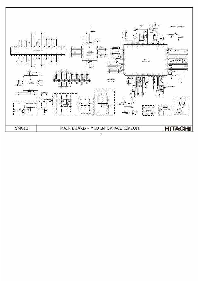
8/12/2019 Hitachi 42PD6700U Plasma TV
http://slidepdf.com/reader/full/hitachi-42pd6700u-plasma-tv 70/79

8/12/2019 Hitachi 42PD6700U Plasma TV
http://slidepdf.com/reader/full/hitachi-42pd6700u-plasma-tv 71/79

8/12/2019 Hitachi 42PD6700U Plasma TV
http://slidepdf.com/reader/full/hitachi-42pd6700u-plasma-tv 72/79
SM012 MAIN BOARD - POWER SUPPLY CIRCUIT
1 6 V
2 2 0 u
C 9 1 4
16V100n
C904
100nC903
5 0 V
1 0 0 n
C 9 0 8
1N4007
D906
47u
C902
5 0 V
4 7 u
C 9 0 9
1N4007
D903
16V100nC910
1 6 V
2 2 0 u
C 9 2 0
1 6 V
1 0 0 0 u
C 9 0 6
VCCA _2V5
STBY _5V
STBY _3V3
V C C A_ 3 V 3
VCC _5V
1N4007
D902
16V100nC923
L913
L912
L 9 0 7
VDDMQ_2V5
VCC _8V
1N4007
D901
V C C D_
3 V 3
1N4007
D900
1N4007
D905
STBY _2V5
5 0 V
4 7 u
C 9 2 1
5 0
V
4 7 u
C 9
0 1
SOT 223FAN1616AS-3.3
IC902
1
23
SOT 223
LD1117IC903
1
23
LM317IC900
1
ADJ2OUT3I N
1k
R902
5 k 6
R 9 0 3
BC848BQ900
BC858BQ901
1N4148
D907
1N4148
D908
1N4148
D909 1 0 k
R 9 1 0
10k
R912
10k
R908
1 0 k
R 9 1
4
1 0 k
R 9 0 7
PROTECTVCC _5V
VCCA _3V3
VCCD _3V3
STBY _3V3
1N4148
D910
VCC _8V
PL900
1
2
3
4
5
6
7
8
9
10
11
12
L904
L903
L902
L901
L900
L905
1 6 V
1 0 0 0 u
C 9 1 2
DIG _DIM _PWM
PDP _GO /BL_ON _OFF
SEL
P L 9 0 2
1 2 3 4 5 6 7
1 2 0 R
R 9 0 9
1 6 V
1 0 0 n
C 9 1 7
5 0 V
2 2 u
C 9 1 8
120R
R911
CS52015-3IC901
1
GND2VOUT3VIN
16V100uC919
1R
R913
16V100nC915
16V100nC922
470R
R900
470R
R901
STBY _3V3
470R
R915
STBY _2V5
L909
PL901
1
2
3
4
5
6
7
8
9
10
VCC _33V
CPU _GO1 /STBY
VCC _12V
V C C_
1 2 V
PROTECT
S900
A _DIM _PWM
16V100nC916
L906
1 6 V
1 0 0 u
C 9 0 0
LM2576
IC223
1
V I N
2
O U
T P U T
3
G N
D
4
F E
E D B A C K
5
O N
/ O F F
22u
L908
VCC _12V
1 6 V
1 0 0 u
C 9 0 5
1 6 V
1 0 0 0 u
C 9 1 1
22u
L910
1 6 V
1 0 0 n
C 9 1 3
22uH_3.9A _SMD
L911330R
R904
S T P S 7 4 5
D 9 0 4
1 _8VMAIN
22u
L915
22u
L914
22u
L916
1 _8VMAIN
1 _8VMAIN
1 _8VMAIN
1 6 V
1 0 0 n
C 9 2 5
1 6 V
1 0 0 n
C 9 2 4
1 6 V
1 0 0 n
C 9 2 6
1 6 V
1 0 0 u
C 9 2 7
1 6 V
1 0 0 u
C 9 2 8
1 0 0 u
C 9 2 9
VL1 _8
VD1 _8
VA1 _8BRT _CNTLA _DIM _PWM
DIG _DIM _PWMS901
2 2 u
C 9 3 0
PANEL_VCC1
VCCA _3V3
VCC _12V
L917
L918
5 V
5V
PL903
1
2
3
4
VCC _5V
P L 9 0 4
1 2 3 4
PDP _GO1 /BL_ON _OFF LG _1 /IR QPDP
S S 3 3
D 9 1 1
S902160R
R905
22u
L919
1 6 V
1 0 0 u
C 9 3 1
1 0 0 n
C 9 3 2
1 0 0 n
C 9 3 3
1 0 0 n
C 9 3 4
1 0 0 n
C 9 3 5
L920
S 9 0 3
S 9 0 4
1 6 V
1 0 0 n
C 9 3 6
1 6 V
1 0 0 n
C 9 3 7
1 6 V
1 0 0 n
C 9 3 8
1 6 V
1 0 0 u
C 9 3 9
1 6 V
1 0 0 u
C 9 4 0
1 6 V
1 0 0 u
C 9 4 1
BLM21B201S
L921
BLM21B201S
L922
MC34063A
IC904
1 SW.COLL.
3 C AP. 6VCC
8DR I.COL.
2 EMITTER
4 G ND
7SENSE
5COMP.
1 0 0 R
R 9 1 6
1 0 0 R
R 9 1 7
R918
10u
L923
V C C_
1 2 V
2 k 2
R 9 1 9
6 k 8
R 9 2 0
56k
R921
3 k 3
R 9 2 2
56p
C942
56p
C943
1 0 0 p
C 9 4 4
22u
C945
10uC946
2 2 u
L 9 2 4
1 N 4 1 4 8
D 9 1 2
V C C_
3 3 V
1.8V_ON /OFF
1.8V_ON /OFF
S905
S T B Y_
2 V 5
F D C 6 4 2 P
Q 9 0 2
1 2 3 4
5 6
Q903
3 3 0 R
R 9 2 3
1 0 k
R 9 2 4
1 0 k
R 9 2 5
16V10u
C947
P A N E L_ V C C 1
P A N E L_ V C C
PANEL_VCC _ON /OFF
AC _INFO
S907
VCCA _3V3S908
S909
S910STBY _3V3
STBY _5V
S911
S 9 1 2
PORT
S913
1 N 4 1 4 8
D 9 1 3
D914
D 9 1 5
STBY _5V
+12V
N.C
N.C
N.C
N.C
MMC SUPPLY
SAP 30030067 ADJ TYPE
67

8/12/2019 Hitachi 42PD6700U Plasma TV
http://slidepdf.com/reader/full/hitachi-42pd6700u-plasma-tv 73/79
SM012 AMPLIFIER BOARD - D-CLASS AMPLIFIER CIRCUIT
15V_AUD
5 0 V
1 n
C 7 8 5
5 0 V
1 0 0 n
C 7 7 7
PL703
1
2
5 0 V
1 0 n
C 7 9 4
2 5 V
1 0 0 u
C 8 1 1
6 3 V
4 7 0 n
C 8 0 8 6
3 V
4 7 0 n
C 8 0 6
5 0 V
1 0 0 n
C 7 8 3
5 0 V
2 2 0 p
C 7 7 9
6 3 V
4 7 0 n
C 8 0 7
PL701 1 2 3 4 5
15V_AUD
5 0 V 1 n
C 7 9 6
M U T E
15V_AUD
50R _100MHZ_3A
L719
40uH
L726
1 8 k
R 7 4 6
40uH
L725
S724
1 u
C 7 8 9
50R _100MHZ_3A
L718
1 6 V
1 u
C 7 9 2
S723
TPA3004D2
IC702
1
S D_ N
O T
2
R I
N N
3
R I N P
4
V 2 P 5
5
L I N P
6
L I
N N
7
A V D D R
E F
8
V R
E F
9
V A R D I F F
1 0
V A R M
A X
1 1
V O L U
M E
1 2
R E F G
N D
1 3 B SLN
14 PVCCL1
15 PVCCL2
16 L OUTN1
17 LOUTN2
1 8 PG NDL1
1 9 PG NDL2
20 LOUTP1
21 L OUTP2
22 PVCCL3
23 PVCCL4
2 4 B SLP
2 5
V C L A M P L
2 6
A G N D 1
2 7
R O S C
2 8
C O S C
2 9
A V D D
3 0
A G N D 2
3 1
V A R O U T L
3 2
V A R O U T R
3 3
A V C C
3 4
M O D E
3 5
M O D E_
O U T
3 6
V C L A M P R
37BSRP
38PVCCR1
39PVCCR2
40ROUTP1
41ROUTP2
42PGNDR1
43PGNDR2
44ROUTN1
45ROUTN2
46PVCCR3
47PVCCR4
48BSRN
1 u
C 7 9 1
1 u
C 7 8 8
2 5 V
2 2 0 u
C 7 8 4
50R _100MHZ_3A
L721
5 0 V
1 n
C 7 8 6
5 0 V
1 0 0 n
C 7 8 2
5 0 V
1 0 n
C 7 8 0
15V_AUD
1 2 0 k
R 7 4 2
5 0 V
1 0 n
C 7 8 1
6 3 V
4 7 0 n
C 8 0 5
15V_AUD
40uH
L724
40uH
L723
15V_AUD
5 0 V
1 0 0 n C
7 7 8
1 6 V
1 u
C 7 7 6
5 0 V
1 0 n
C 7 9 3
1 u
C 7 9 0
5 0 V
1 0 0 n
C 8 0 2
5 0 V
1 0 0 n
C 8 0 1
2 5 V
2 2 0 u
C 7 7 5
PL702
1
2
2 5 V
2 2 0 u
C 8 0 3
3 3 k
R 7 4 5
50R _100MHZ_3A
L722
1 u
C 7 8 7
5 0 V
1 n
C 7 9 5
1 0 0 k
R 7 5 6
BC848BQ709
PL707
1 2
MUTE
LM809
IC703
1
2
BC848BQ710
S732
S 7 3 3
S 7 3 4
2 5 V
1 0 0 n
C 8 1 3
2 5 V
1 0 0 n
C 8 1 4
2 5 V 1
0 0 n
C 8 1 5
2 5 V
1 0 0 n
C 8 1 6
BSN20Q603
BSN20Q604
S735
S736
S S 3 3
D 9 0 4
LM2576
IC708
1
V I N
2
O U T P U T
3
G N D
4
F E E D B A C K
5
O N / O F F
1 k 8
R 7 5 4
3 5 V
4 7 0 u
C 8 2 1
S730
2 2 k
R 7 5 5
PL700
1
2
3
4
22uH_3.9A _SMD
L109
S T P S 7 4 5
D 9 0 1
15V_AUD
22u
L904
22u
L727
22u
L729
2 5 V
1 0 0 0 u
C 8 2 2
2 5 V
1 0 0 0 u
C 8 2 0
1 2 k
R 7 6 5
1 2 k
R 7 6 6
3 k 3
R 7 6 7
5 0 V
2 2 n
C 8 1 7
5 0 V
2 2 n
C 8 1 8
S737
S 7 3 8
9k1R 768
1 5 V_
A U D
1k
R 770
1k
R 771
MUTE_3V3
2 5 V
1 0 0 n
C 8 2 3
2 5 V
1 0 0 n
C 8 2 4
MUTE_3V3
25V100n
C825
2 5 V
1 0 0 n
C 8 2 6
4k
R 772
BC848B
Q715
3 k 3
R 7 7 3
S739
MAI N _ O UT _R
HIGH=ON
LOW=OFF
MAI N _ O UT _L
N.C
R ESET OUT
vcc 5v
3
68

8/12/2019 Hitachi 42PD6700U Plasma TV
http://slidepdf.com/reader/full/hitachi-42pd6700u-plasma-tv 74/79
SM012 FRONT AV BOARD CIRCUIT
F R O N T_
A U D I O_
R
H P_
R
A
WHITE_FAVJK105
F R O N T_ V I D E O
L I N E_
O U T_
R
H E A D P H O N E
P L 1 0 0
1 2 3 4 5 6 7 8
H P_
R
F R O N T_
A U D I O_ L
F R O N T_
A U D I O_
R
L I N E_
O U T_
R
L I N E_
O U T_
S U B
S V H S_
C
A
WHITE_FAVJK103
A
1P _R ED _FAVJK102
F R O N T_
A U D I O_ L
4P
JK100
2
3
S V H S_
C
L I N E_
O U T_ L
P L 1 0 3
1
S V H S_
Y
S V H S_
Y
H P_ L
P L 1 0 1
1 2 3 4
S V H S_
C
H P_ L
H E A D P H O N E
A
YELLOW _FAVJK101
12
F R O N T_ V I D E O
P L 1 0 2
1 2 3 4
L I N E_
O U T_
S U B
L I N E_
O U T_
R
PHJACK
JK104
1 2 3
4 5 6
7 8 9
A
WHITE_FAVJK106
P L 1 0 4
1 2 3 4 5 6 7 8 9 1 0
1 1
1 2
F R O N T_ V I D E O
H P_ L
F R O N T_
A U D I O_
R
F R O N T_
A U D I O_ L
H P_
R
H E A D P H O N E
L I N E_
O U T_
S U B
L I N E_
O U T_ L
A
1P _R ED _FAVJK107
S V H S_
Y
L I N E_
O U T_ L
P L 1 0 5
1 2 3 4
R 1 0
0
R 1 0 1
R 1
0 4
R 1 0 5
R 1 0 6
50V33p
C100
50V33p
C101
50V33p
C102
50V100p
C103
50V100p
C104
50V100p
C108
50V100p
C110
50V100p
C109
50V4n7
C106
50V4n7
C107
BZT55C10
D101
BZT55C10
D103
BZT55C10
D104
BZT55C10
D102
BZT55C10
D100
BZT55C10
D105
BZT55C10
D107
BZT55C10
D106
BZT55C10
D108
BZT55C10
D109
S 1 0 0
S 1 0 1
L 1 0 0
6 0 0 R_ 1 0 0 M H Z_
2 0 0 m A
L 1 0 1
L 1 0 2
L 1 0 3
L 1 0 6
L 1 0 5
L 1 0 4
L 1 0 8
L 1 0 7
L 1 0 9
L 1 1 0
L 1 1 1
L
1 1 2
L 1 1 3
L 1 1 4
L 1 1 5
L 1 1 6
L 1 1 7
L 1 1 8
L 1 1 9
L 1 2 0
50V100p
C105
R 1 0 2
R 1 0 3
R 1 0 7
R 1 0 8
R 1 0 9
R 1 1 0
1
4
3
12
312
3
12
3
12
3
12
3
69

8/12/2019 Hitachi 42PD6700U Plasma TV
http://slidepdf.com/reader/full/hitachi-42pd6700u-plasma-tv 75/79
SM012 CIRCUIT BOARDS
1 2 3
8 7 6 4 & 5
1. Y-SUS Board (TS06288)
3. X-SUS Board (TS06287)
6. IDTV Board 17DB23 (VS20252456)
8. Joint Board 17DB21 (VS20252456)
7. Main Board 17MB15-E5 (VS20251818)
5. Filter Board 17FL2-02 (VS20225622)
4. Audio Board 18AMP05 (VS20217003)
2. Power Board (VS30043468)
19.3. CIRCUIT BOARDS
70

8/12/2019 Hitachi 42PD6700U Plasma TV
http://slidepdf.com/reader/full/hitachi-42pd6700u-plasma-tv 76/79
SM012 PCB LAYOUTS
C61
L 1 1 1
L 1 1 0
L 1 1 9
L 1 0 8
L14 C256R136
S 3 0 4
C 3 1 5
S 3 0 2
S303
R 1 4 8
S 3 0 1
IC501
R19
R126IC5
R59
L 1 3
C 2 5 7
S 3 0 5
L12 C 3 0 7
C 3 0 8
C 3 0 5
C 3 1 0L16
C311
VpRxD
17PING08VER:E218/06/04
C133 R 1 2 1
I C 1 0 3
C52
C51
C50
C37
P L 1 0 1
C53
C25
S1
C110 R 1 1 8
R 1 1 9
C117C114D180
C 1 1 8
C111 C 1 2 2
R123
PL106
PL100 X 1 0 0
R747
R115
L10 I C 1 0 2
R127
L 1 1 2C103
C 1 2 0
L113
C132
C305 R 1 1 4
R 1 1 2
R 1 1 3R310
R 1 2 2
R300
C134 R 1 2 0
D101
R 7 4 3
R 7 4 2
R 7 4 1
R 7 4 0
S2R110
R128R319
C119
C707
L15
C130R137R318
C 3 1 2R136
L105L106
R747R746R745R744R312R311
IC100
C128C126
2.5V
C 1 2 9
SDA
C509R146
C124
R661 R660
R662
R 6 3 1
R 6 0 3
IC545 I C 9 0 2
R530
C 6 0 5
C 6 0 1
C 6 0 6
C 5 1 0
R 5 3 2
IC600
IC648
R 5 0 2
R444
C 6 0 3
C604 PL600 C 6 0 0
C 6 0 2
IC647
C475
C486
R657
R604
5V
R443 C608 C651 R652
R466 C439C127R160
R 1 5
9
I C 4 0 2
C452
C 4 5 6
C 4 7 9
S 4 0 1
C476C485
S D A C 1
S D A C 2
R659
Q 6 0 0
R 5 0 0
R 6 5 8
R 5 1 0
C438
C 6 0 1
R 6 4 5
C437
L610 3.3V
R 4 5 9
C422C434X400
L413
C 4 4 0
C469
C470 R 5 5 0
R 5 6 9
R 5 5 3
IC401C491 R407
C404R468
C423
C 4 2 6
C 4 7 3
R467
C481 C 4 7 2
L404
C410 C 4 1 1
C 4 1 4
C429 C428L400 C445
C 4 4 6
C 4 2 1
C 4 8 9
R411 C420L412
Q402
R475 R415
C493
TU400
C 4 1 6
R161
C 4 8 8
R400 Q403
C 4 0 8
S 4 0 2
L 4 0 2
C415Q401
R 4 1 0 L
4 1 1
C 4 6 2
R 4 4 9
C 4 6 1
C 4 6 4
C463R451
C460
C 4 1 2
R 4 2 8
R 4 7 0
S 4 0 6
C 4 6 4
S 5 1 5
C 1 2 5
R105 C131
R104 C102 R338 R339C218
S514 R 3 0 7
R 3 0 8
L101
L207 R231
C 2 2 0
R 2 3 2
C402
R409C414R408
R413
C409
L 6 2 3
R 4 1 1
C 4 0 5
D400
R403Q400 R402
C491 R
4 0 1
C22S513
C406 L 4 0 1
R405R404 R
4 5 0
C 4 5 9
D402R452 R431 R432
D401
Z 4 0 0
R102
R144
L103 L102
IC300
IC201
C 1 1 6
C 1 0 4 C135
C137
R201 R290 L206C205
R 2 0 3
R221
L220
C211
C459C205C200L205
C203
R202
L204
C207
C202
R 2 0 5 R
2 0 4
P L 2 0 2
L 2 1 6
R222 Q121
Q 1 2 0
C 2 9 5
C236
C 2 5 2
R125
R139C255
C212
L 2 2 2
L 2 2 1
R108
IC101
C148 PL105PL203
L217
C255R213
C457L605
C147
L 2 1 2
L 2 1 8
L 2 1 4
L 2 1 3
L 2 1 9
L 2 1 1
L 2 1 0
L 2 0 9
L 2 0 8
L 2 1 5
C145
C146C109
C204
L 2 0 3
C254
Q122
C275
R214
R223
D200
C401 C 4 0 3
R 2 6 3
L 8 2 6
R 2 3 6
R 2 6 0
C 2 2 7
R 2 1 2
R 2 0 6
Q203
C 2 0 1
R 2 9 5
R262
R224C214
C 2 2 3
R 2 0 6
R 2 1 5
R 2 1 7
C213
R 2 4 1
R238D206
R 2 3 9 R
2 3 7
Q207 Q204 Q205
R238Q201 D202
R 2 1 0
R 2 1 6
P L 2 0 1
S400
R 2 3 0
R 2 1 8
R 2 2 0
C 2 2 9
R 2 1 9
R 2 2 7
C 2 2 5
R 2 2 8
R 2 2 5
C 2 2 1
PL200
P L 1 0 6
C 5 3
X 1 0 0
C 4 1 P L 1 0 1
C 1 0 3
C 1 3 4
3 . 3 V
5 V
3 3 V
1 2 V
G N D
G N D
2 . 5 V
C 1 3 3
L 1 7 C 3 1 3
P L 1 0 1
T R I G G E R O U T
J T A C R S T
T D O
T R I G G E R I N
T O J
T C K
T M 5
T R S T
R 3 3 6
R 3 3 7 C 1 3 2
L 1 0 7
R 1 4 8
R 3 0 5 R 1 0 6
C 3 0 0
C 1 1 2
L 9
C 3 0 3
L 1 1
C 3 0 4
L 7
C 3 0 2 4
C 3 0 1
C 1 2 3
C 1 1 5
R 3 0 6
C 1 2 1
C 1 3 7 C 1 3 5
C 2 3 6
C 2 1 2
C 3 0 6
L 8
T P 3 0 1
Z 4 0 0
C 4 0 6
C 4 5 3
L 4 0 5
C 4 0 1
C 2 1 1
P L 2 0 3
P L 2 0 2
C 2 0 4
R 4 4 1 C 4 8 0
P L 1 0 5
P L 2 0 1 P L 2 0 0
G N D
R E D
G N D
B L U E
G N D
G R E E N
G N D
T V O U T
C 4 5 8
C 4 8 4
T U 4 0 0
C 4 9 3
C 4 7 2
C 4 1 0
C 4 8 1 L 4 0 0
X 1 0 0
C 4 3 3
C 4 7 4
R 4 5 6
C 4 8 5
C 4 8 7
C 4 7 6
C 4 5 2
C 4 3 5
C 4 3 0
R 4 4 8
R 4 4 7
R 4 1 8
R 4 1 9
C 4 9 2
R 1 3 5
R 1 0 2
R 1 0 1
C 1 1 3
C 3 1 5
R 1 5 1 R 1 0 0
R 1 5 2
R 1 0 3
I C 3 0 3
C 4 3 6
C 4 8 6
C 4 7 5
C 4 5 2
C 3 1 4
P L 6 0 0
IDTV BOARDTOP (COMPONENT) SIDE BOTTOM (SOLDER) SIDE
C822
L727
PL741
R 7 7 1
R 7 7 7
R 7 7 6
S 7 2 4
L109L904
R775
R774
R754R755
IC708
PL707
S733 Q710
S732
IC703
C821
L729
PL700 C834
R767 Q709C818 S737R766 C817
R756
C807 L725
S734
L726
C808 PL702
UA
C776S738C778C779R742C792
C811
C831
Q 6 0 4
C813
C 7 9 5
C 7 8 6
L 7 2 2
C 8 0 2
C 7 9 4
C814
C 7 7 1
C 7 8 3
Q 6 0 3C791
C789C790
C788
R746R745
L 7 2 1
C793
C 8 0 1
C 8 2 6
S 7 2 5
R771
C820
C835
C 8 2 3
R 7 7 3
R 7 6 5
S739C787
C714
C782
Q 7 1 5
L 7 1 8
C 7 8 0
C 8 1 6
IC702
C815C781
C785 C786 L 7 1 9
R754
R772C825
L723L724
C806 PL703
S 7 3 5
C 8 2 4
S 7 3 6
D904D901
18AMP05-2
121205LF
L 7 2 4 L 7 2 3
P L 7 0 1
L 7 2 7
D 9 0 1 C 8 3 1 C
8 2 8
C 8 3 0
C 8 3 2
C 8 0 5 C
8 3 5
C 8 0 6
P L 7 0 3
C 8 3 7
C 8 1 1
C 8 3 3
C 8 2 9
C 8 7 7
C 8 3 4 C
8 0 5
P L 7 0 2
L 7 2 6
L 7 2 5 C 8 0 7
C 8 3 6
L 7 2 9
C 8 2 0
P L 7 0 0
C 8 2 1
P L 7 0 7
R 7 7 4
R 7 7 5
L 9 0 4
C 8 2 2
AMPLIFIER BOARD
TOP (COMPONENT) SIDE
BOTTOM (SOLDER) SIDE
FRONT AV BOARD
JK101
PL100 PL102PL103
PL101
PL105
104
UA
JK100
17FAV15-2230805
32-37XXPL104
TOP (COMPONENT) SIDE
PL102 PL100
PL103
PL101
PL105
PL102
R103 R102
R104 L116 R105
C108 L117
C109
L118
R106 L120 L114
L115
D107 D108 D109
L119
C110
D106
L113
C 10 5 L 11 2
L110
C107
C106
JK104
JK107JK106JK105 JKI03 JK102 JK101D105
L111 L108
R 1 01 L 10 9 R 1 00 L 1 07
D104
C104
L106
D103
C103
S100
S103
L105
L104
D102
R108
R107
L103
L101
L100
C102
C100
D100
C101
L102
D101
JK100
BOTTOM (SOLDER) SIDE
19.4 PCB LAYOUTS
71

8/12/2019 Hitachi 42PD6700U Plasma TV
http://slidepdf.com/reader/full/hitachi-42pd6700u-plasma-tv 77/79
SM012 CONNECTOR DIAGRAM
KEYPADFRONT AV BOARD
PL101 PL102
PL201 PL1002 PL301
PL1
PL606
PL1
PL600 PL904
PL104
PL1
PL308
PL1001 PL903
PL100
PL900 PL902 PL103 PL901 PL1003
PL203
PL101
PL202
PL106
CN42CN26
PL4
PL804PL803PL101PL802PL803
PL805 PL800 PL801 PL102
PL701 PL707 PL700
PL702 PL703
CN2 CN11 CN10
CN32
CN61 CN69 CN64 CN23
ON-OFFSWITCH
PL101PL100
RIGHTSPEAKER
LEFTSPEAKER
PL3
PL2
PL1
PANEL
PANELCONTROL UNIT
INFRARED BOARD
MAIN BOARD
DAUGHTER BOARD
CN24
DAUGHTERBOARD IDTV MODULE
BOARD
POWER (SMPS)
BOARD
PANEL DRIVERCIRCUIT1
XSUS BOARD
AMPLIFIERBOARD
ABUS-LBOARD
PANEL DRIVERCIRCUIT2
YSUS BOARD
AC INPUT
FILTER BOARD
19.4 . CONNECTOR DIAGRAM
72

8/12/2019 Hitachi 42PD6700U Plasma TV
http://slidepdf.com/reader/full/hitachi-42pd6700u-plasma-tv 78/79
THE UPDATED PARTS LIST
FOR THIS MODEL IS
AVAILABLE ON ESTA

8/12/2019 Hitachi 42PD6700U Plasma TV
http://slidepdf.com/reader/full/hitachi-42pd6700u-plasma-tv 79/79
Hitachi, Ltd. Tokyo, JapanInternational Sales Division
THE HITACHI ATAGO BUILDING,
No. 15 –12 Nishi Shinbashi, 2 – Chome,Minato – Ku, Tokyo 105-8430, Japan.
Tel: 03 35022111
HITACHI EUROPE LTD,
Whitebrook ParkLower Cookham RoadMaidenheadBerkshireSL6 8YAUNITED KINGDOMTel: 01628 643000Fax: 01628 643400Email: [email protected]
HITACHI EUROPE S.A.
364 Kifissias Ave. & 1, Delfon Str.152 33 Chalandri AthensGREECE
Tel: 1-6837200Fax: 1-6835964Email: [email protected]
HITACHI EUROPE GmbH
Munich OfficeDornacher Strasse 3
D-85622 Feldkirchen bei MünchenGERMANY
Tel: +49-89-991 80-0Fax: +49-89-991 80-224Hotline: +49-180-551 25 51 (12ct/min)Email: [email protected]
HITACHI EUROPE S.A.
Gran Via Carlos III, 86, planta 5Edificios Trade - Torre Este
08028 BarcelonaSPAINTel: +34 93 409 2550Fax: +34 93 491 3513Email: [email protected]
HITACHI EUROPE srlVia Tommaso Gulli N.39, 20147Milano, ItaliaITALY
Tel: +39 02 487861Tel: +39 02 38073415 Servizio ClientiFax: +39 02 48786381/2
Email: [email protected]
HITACHI Europe ABBox 77 S-164 94 KistaSWEDEN
Tel: +46 (0) 8 562 711 00Fax: +46 (0) 8 562 711 13Email: [email protected]
HITACHI EUROPE S.A.S
Lyon OfficeB.P. 45, 69671 BRON CEDEXFRANCETel: +33 04 72 14 29 70Fax: +33 04 72 14 29 99Email: [email protected]
HITACHI EUROPE LTD (Norway) AB STRANDVEIEN 181366 Lysaker NORWAYTel: 67 5190 30Fax: 67 5190 32Email: [email protected]
HITACH EUROPE AB
EgebækgårdEgebækvej 98DK-2850 NærumDENMARK
Tel: +45 43 43 6050Fax: +45 43 60 51Email: csgnor@hitachi eu com
HITACHI EUROPE AB
Neopoli / Niemenkatu 73FIN-15140 LahtiFINLANDTel : +358 3 8858 271Fax: +358 3 8858 272Email: [email protected]