highly conductive and transparent reduced graphene oxide/aluminium doped zinc oxide nanocomposite...
TRANSCRIPT
Optical Materials xxx (2013) xxx–xxx
Contents lists available at ScienceDirect
Optical Materials
journal homepage: www.elsevier .com/locate /optmat
Highly conductive and transparent reduced graphene oxide/aluminiumdoped zinc oxide nanocomposite for the next generation solar cellapplications
0925-3467/$ - see front matter � 2013 Elsevier B.V. All rights reserved.http://dx.doi.org/10.1016/j.optmat.2013.09.012
⇑ Tel.: +886 972506900; fax: +886 73645589.E-mail address: [email protected]
Please cite this article in press as: I.Y.Y. Bu, Opt. Mater. (2013), http://dx.doi.org/10.1016/j.optmat.2013.09.012
Ian Y.Y. Bu ⇑Department of Microelectronics Engineering, National Kaohsiung Marine University, 81157 Nanzih District, Kaohsiung City, Taiwan, ROC
a r t i c l e i n f o
Article history:Received 29 June 2013Received in revised form 2 September 2013Accepted 9 September 2013Available online xxxx
Keywords:Aluminium doped zinc oxideReduced graphene oxideCompositeTransparentConductiveHybrid
a b s t r a c t
In this paper, aluminum-doped zinc oxide(AZO)/reduced graphene oxide nano-composite thin films aresynthesized by a one-pot, solution-processed method. The nanocomposite film has been extensivelycharacterized using scanning electron microscopy (SEM), X-ray-diffraction (XRD), energy dispersivespectroscopy (EDS), Hall effect measurement and UV–Vis spectroscopy. It is found that the controlledaddition of reduced graphene oxide into AZO can lower the film’s resistivity without causing significantdegradation of optical transparency. In addition, nanocomposite films post-annealed at process temper-ature at 500 �C possesses the lowest resistivity and the highest optical transmittance and that furtherincreases in the annealing temperature degrades the film’s property due to nucleation of other phasesof the AZO.
� 2013 Elsevier B.V. All rights reserved.
1. Introduction
Graphene, which consists of a single layer of two-dimensionalcarbon sheet, has attracted intensive research interests due to itsexcellent electrical, mechanical, and optical properties. Its notablecharacteristics include tunable band gap [1], high mobility [2], andhigh flexibility [3]. Combination of these traits has lead to theinvestigation of using graphene as the transparent conductive filmfor the next generation flexible electronic devices. In particular,graphene has been propose to replace the traditionally usedindium tin oxide [4–6], which is liable to crack under mechanicalstress, in the organic based electronic devices, such as organic solarcells [7] and thin film transistors [8].
Graphene also possesses excellent chemical stability and highspecific surface area, which enable it to be integrated into othermaterials without difficulties [9]. Previous studies have success-fully demonstrated the feasibility of incorporating graphene intoorganic polymers [10,11], metallic nanoparticles [12–14], and inor-ganic nanostructured compounds such as ZnO [15,16], TiO2
[17,18], and Fe3O4 [19]. The combination of ZnO with graphenehas shown interesting properties that are absent in the individualmaterial. Owing to structural defects, the as-deposited ZnO isgenerally n-type [20] and its resistivity can be further reduced by
Al doping [21,22]. Previous studies of ZnO/graphene compositefilms have revealed their excellent field emission properties [23],photocatalyst [16,24], anti-corrosion coating [25] and potentialapplication in batteries [26]. Whilst there are several studies onZnO/graphene based composite materials [27,28,26,29], to our bestknowledge, there is no study on composite materials that are basedon AZO/reduced graphene oxide. The current study focuses uponthe applicability of AZO/reduced graphene oxide composite thinfilm for transparent conductive electrodes. Optoelectronic proper-ties were investigated by using scanning electron microscopy(SEM), X-ray diffraction (XRD), UV–Vis spectroscopy, and Hall ef-fect measurements.
2. Experimental procedure
All chemicals used in this study were of regent grade and usedwithout further purification. The AZO solution was prepared bymixing 0.7 M of zinc acetate in isopropanol with 1 wt% AlCl3. Themixture was stirred at 70 �C for 60 min in order to yield a transpar-ent homogeneous solution.
Graphene oxide (GO) was prepared from graphite flakes byusing the modified Hummers method [30]. In a typical experimen-tal procedure, 1.8 g of graphite powder was mixed with NaSO4
(1.8 g) in an ice cooled beaker. Then KMnO4 (7 g) was graduallyintroduced into the graphite/acid solution. The reaction usuallylasted for 3 h. Subsequently, 100 ml of distilled water was added

2 I.Y.Y. Bu / Optical Materials xxx (2013) xxx–xxx
into the solution, which resulted in an exothermic reaction thatwas cooled by ice to keep the temperature below 100 �C. Then,100 ml of H2O2 was added into the solution to remove the residualKMnO4. At this stage, the resultant mixture became effluent withbubbles and its color changed from brown to bright yellow, whichwas a well-recognized sign of GO formation. Finally, the solution-mixture was repeatedly filtered (Whatman anodisk 20 nm) andwashed with diluted HCl acid and water several times to removethe remaining metal ions. The collected GO solids were then centri-fuged in water at 5000 rpm and converted into reduced grapheneoxide by using a vacuum furnace set at 700 �C under hydrogenflow.
The structural and chemical properties of the derived AZO/re-duced graphene oxide nanocomposites were evaluated by usingan FEI Quanta 400 F environmental scanning microscope, equippedwith energy dispersive spectroscopy (EDS). A Siemens D5000 X-rayDiffractometer with Cu Ka radiation was used to measure the XRDpatterns. Electrical measurements were obtained through the Hallmeasurements, using a four-point probe in a Van der Pauw config-uration, in order to determine resistivity and carrier concentration.
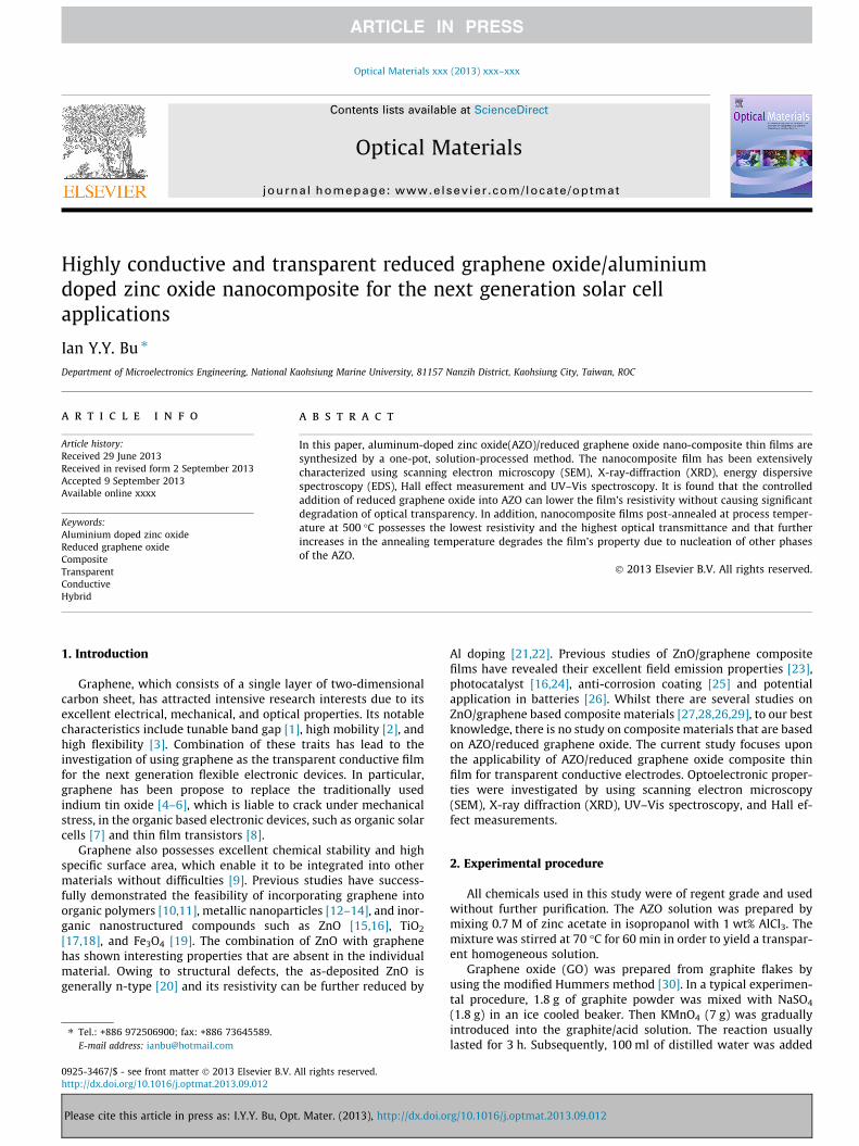
Fig. 1. SEM image of the sol–gel derived AZO incorporated with reduced graphene oxidmarks the area of EDS analysis), (e) close up on one of the graphene flake on surface (scale(scale bar 200 nm).
Please cite this article in press as: I.Y.Y. Bu, Opt. Mater. (2013), http://dx.doi.o
The photoluminescence (PL) measurements were carried out byusing a 325 nm He/Cd laser (Jasco Model FP-6000). UV–Vis NIR(Hitachi U-4100) was used to determine the optical transmittanceand the Tauc gap. The detailed morphology of the synthesisedreduced graphene oxide sheets was evaluated using a PhilipsCM-200 TWIN transmission electron microscope (TEM) operatedat 20 kV.
3. Results and discussion
Fig. 1 shows the SEM images of the deposited AZO/reducedgraphene oxide thin film on Corning glass as a function of heattreatment temperature. It can be observed from Fig. 1(a)–(d) thatall of the films appear to have been uniformly coated with grains,characterized by increasing diameters with higher post annealingtemperatures. By increasing the post annealing temperature from400 �C to 550 �C, the grain size increases from 20 nm to around50 nm. This enhancement in grain size can be attributed to theaccelerated atom diffusion, which leads to enhanced crystalgrowth. It is interesting to note that, although a significant quan-
e and post sintered at (a) 400 �C, (b) 450 �C, (c) 500 �C, (d) 550 �C (the square boxbar 10 lm) and (f) TEM image of the derived reduced with reduced graphene oxide
rg/10.1016/j.optmat.2013.09.012

Element CKOK
ZnLAlKMatrix
09.4016.61 62.0511.94
Wt%
Correction
At%24.3732.3129.5413.78ZAF
Fig. 2. EDS compositional analysis of the AZO/with reduced graphene oxide samples.
I.Y.Y. Bu / Optical Materials xxx (2013) xxx–xxx 3
tity of reduced graphene oxide is mixed into the precursor solu-tion, only few graphene nanosheets appeared on the surface ofthe thin film. This phenomenon suggests that most of the reducedgraphene oxides have been embedded into the films. Fig. 1(e)shows one of the chemically exfoliated reduced graphene oxidesheets on the thin film surface. Clearly, some of the reduced graph-ene oxide flakes have been restacked during the sol–gel synthesis.Similar restack of reduced graphene oxides (2–10 layers) has beenobserved in the literature [31,32] and can be successfully pre-vented by inserting carbon nanotubes [33] or careful controlleddeposition of the graphene sheets [34]. Fig. 1(f) shows the typicalTEM image of the reduced graphene oxide nannosheets (prior tobeing introduced into AZO precursor) that contain no more than4 layers of graphene. Evidently, both SEM and TEM images suggestthat the sol–gel process is capable of restacking the graphene lay-ers, possibly due to the dehydration process, as solvents tend toprevent the restacking process [34].
The reduced graphene oxide sheet is uniformly coated with AZOand wrapped around fibrous materials with a diameter of 500 nmand an average length of 5 lm. Previous studies have suggestedthat such a wrinkling of sol–gel derived thin films is caused byeither the lack of OH groups in the precursor sol or stress relaxa-tion due to the difference in thermal expansion coefficients[35,36]. Because the wrinkles appeared only in the regions nearthe graphene flakes, the difference in thermal coefficients shouldbe the most probable cause for the wrinkled network formation.EDS analyses (insert of Fig. 1(d) are performed in order to deter-mine the chemical composition of the hybrid AZO/reduced graph-ene oxide thin film. Fig. 2 shows the representative resultsobtained by the EDS compositional analysis of the AZO/reducedgraphene oxide samples. As expected, the derived film consists ofZn:O:Al:C at a ratio of 39:37:2:22.
Fig. 3 shows the XRD patterns of the AZO/reduced grapheneoxide composites that are annealed at different temperatures. Allof the diffraction patterns can be indexed to the hexagonal wurtiz-ite structure of ZnO JCPDS card (JCPDS 76-0704), with a polycrys-talline structure. The XRD peaks reveal that the derivednanocomposite films are preferentially c-axis oriented at (002).Fig. 3 clearly shows that the diffraction pattern peaks intensity in-creases as the post annealing temperature increases from 400 to500 �C. It is worth noting that further increase in the annealingtemperature to 550 �C results in a decrease in the (002) orienta-tion, probably due to nucleation of other ZnO phases.
Fig. 4 shows the room temperature PL spectra of the AZO/re-duced graphene oxide thin film as a function of annealing temper-atures. It can be observed that, as the annealing temperatureincreases from 400 to 550 �C, the PL spectrum of the AZO/reducedgraphene oxide possesses a single broad peak centered at around
Please cite this article in press as: I.Y.Y. Bu, Opt. Mater. (2013), http://dx.doi.o
420–440 nm. Typically, there are two PL peaks associated withZnO, centered at 550 nm (green) and 380 nm near the band edge(NBE). The NBE PL peak is believed to have originated from theannihilation of free excitons through recombination. On the otherhand, the green emission is presumed to be defect-related and isascribed to zinc interstitials and oxygen vacancies in the ZnO film.By deconvolute the peaks of the PL emission spectrum, it can beshown that the spectrum consists of a combination of two peaksat 435 and 475 nm, respectively. Whilst the PL emission peak cen-tered at 435 nm is attributed to the reduced graphene oxide [37],the peak at 475 nm is associated with the presence of various pointdefects (oxygen vacancies) [38,39] or formation of ZnO quantumdots on reduced graphene oxide [39]. The PL emission data showthat the introduction of reduced graphene oxide has resulted in adominant blue emission at 430 nm that suppresses the UV emis-sion peak at 380 nm.
Fig. 5 shows the optical transmittance of the AZO/reducedgraphene oxide composite as a function of post annealing temper-atures. The as-deposited AZO/reduced graphene oxide films aretransparent to visible light, with the average optical transmittancevalue of films in excess of 86%. It is shown that the average opticaltransmittance is generally insensitive to the post-annealing heattreatment and slightly increases with incremental increase of tem-perature (400, 450 and 500 �C). However, when the films are an-nealed at 550 �C, the average optical transmittance decreases to81%. This result indicates the fluctuation in structural property ofthe composite film as a function of annealing temperatures. Thebasic material requirements of transparent conductive films is thatthe films should achieve transmission greater than 80% and resis-tivity less than 10�4 X cm. The high transmittance of the AZO/re-duced graphene oxide composite has confirmed that our samplesare of excellent quality, which is comparable to those formed bymore complicated techniques such as CVD and sputtering. Becauseour AZO/reduced graphene oxide composite is predominately AZO,it is reasonable to consider it to have a similar optical property ofAZO. Transparent AZO film, a direct band gap semiconductor, hasan absorption coefficient which is defined by the followingequation:
ðahvÞ ¼ Aðhv � EgÞ12 ð1Þ
where A is a constant; a the absorption coefficient; and hv thephoton energy. The optical band gap energy Eg can be estimatedfrom the Tauc plot. In the current study, the extracted Eg valuesare 3.29, 3.34, 3.40, and 3.37 eV for AZO/reduced graphene oxidethin films as-deposited and annealed at 300, 400, 500 and 550 �C.The extracted Eg are almost identical to those of intrinsic ZnO(i.e., 3.37 eV).
rg/10.1016/j.optmat.2013.09.012

Fig. 3. XRD pattern of AZO/with reduced graphene oxide composite post-sinteredat 400–550 �C.
4 I.Y.Y. Bu / Optical Materials xxx (2013) xxx–xxx
Fig. 6 presents the Hall effect measurement, which shows theeffect of annealing temperature on the resistivity of AZO/reducedgraphene oxide sheet. Owing to the improved crystallinity andreduced grain boundaries defects, the sheet resistivity of the filmdecreases with incremental increase of annealing temperature.However, as the annealing temperature exceeds 550 �C, the resis-tivity rises due to the decreased crystallinity as indicated in theXRD data. Because the benefit of conductive carbon fillerdiminishes after it reaches the percolation threshold, the overallresistivity of the deposited film is not influenced by the conductiv-ity of the reduced graphene oxide. Similar result has been observedfrom the addition of carbon nanotubes into polymer [40]. Evalua-
Fig. 4. Photoluminescence spectra of AZO/with reduced grap
Please cite this article in press as: I.Y.Y. Bu, Opt. Mater. (2013), http://dx.doi.o
tion of the optical transmittance data and sheet resistivity clearlysuggests that the best performing film is deposited at the postannealing temperature around 500 �C. The obtained resistivity iscomparable with those obtained by sol–gel deposited AZO thinfilms at higher processing temperature (�900 �C) [41]. A directcomparison can provide us with useful insights into the propertyof the AZO/reduced graphene oxide composite. In general, sol–gelderived AZO thin films are c-axis oriented with grain size of around30 nm; resistivity around 10�2 X cm; carrier concentration in theregion of 1019 cm�3; optical band gap around 3.40 eV; and possessan optical transparency of around 70–75% [42]. On the other hand,the AZO/reduced graphene oxide composite, deposited under asimilar condition, is also c-axis oriented with grain size of around40 nm; resistivity around 5 � 10�2 X cm; carrier concentration inthe region of 1019 cm�3; optical band gap around 3.40 eV; andhas an optical transparency greater than 86%. Clearly, the additionof reduced graphene oxide significantly improves the optical trans-parency of the films, without causing significant influences on itsstructure and resistivity. It is evident from our study that the mostlikely reason is the degree of preferential orientation. Whilst ourXRD data in Fig. 3 shows only a single peak at (002), the pristineAZO exhibits two additional peaks at (100) and (101), respectively[42]. Essentially, the precipitation of other crystal phases will scat-ter lights and lower the optical transmittance. Consequently, thelow temperature process of the current study offers a distinctadvantage by adding the reduced graphene oxide into the precur-sor sol. Of particular interest is that this study has yielded thinfilms with AZO nanocrystals that connect the reduced grapheneoxide flakes together without adversely affecting their opticaltransparency. Previous studies [43,44] have shown that the lowconductivity of graphene flake-based film is caused by the poorcontact between graphenes in void areas. Nevertheless, by filling
hene oxide composite thin films sintered at 400–550 �C.
rg/10.1016/j.optmat.2013.09.012

Fig. 5. Optical transmittance of AZO/with reduced graphene oxide composite postsintered at 400–550 �C.
Fig. 6. Resistivity of AZO/with reduced graphene oxide nanocomposite as afunction of post sintering temperature 400–550 �C.
I.Y.Y. Bu / Optical Materials xxx (2013) xxx–xxx 5
these voids with highly conductive AZO crystals, the conductivitycan be increased without causing significant degradation of theoptical transparency [43,44].
4. Conclusions
Transparent and conductive AZO/reduced graphene oxide nano-composite thin films have been successfully obtained by a sol–geldeposition method. Effects of the post annealing temperature onthe nanocomposite’s optoelectronic properties are investigatedby using SEM, TEM, EDS XRD and Hall measurements. Owing tothe enhanced crystallization of the AZO, the resistivity decreaseswith the incremental of post annealing temperature. There is aclear tendency of improved optical transparency for films annealedfrom 300 to 450 �C. However, due to the nucleation of differentphases of the films and wrinkled formation, such an enhancementin optical transparency will be disrupted in films sintered at higherannealing temperatures (500 and 550 �C). PL data suggests that theintroduction of reduced graphene oxide into AZO results in PLemission at 435 nm and suppresses the commonly observed UVemission peak at 380 nm. There is also a synergistic effect in thecombined nanocomposite and the reduction in resistivity is
Please cite this article in press as: I.Y.Y. Bu, Opt. Mater. (2013), http://dx.doi.o
believed to be caused by the reduced contact resistance and thefilling of voids between the graphene sheets.
Acknowledgement
The author I.Y.Y. Bu would like to thank National Science Coun-cil, under the Grant NSC 98-2218-E-022-001 and NSC 99-2628-E-022-001 for financial support.
References
[1] M.Y. Han, B. Özyilmaz, Y. Zhang, P. Kim, Physical Review Letters 98 (2007)206805.
[2] K.I. Bolotin, K. Sikes, Z. Jiang, M. Klima, G. Fudenberg, J. Hone, P. Kim, H.Stormer, Solid State Communications 146 (2008) 351–355.
[3] C. Lee, X. Wei, J.W. Kysar, J. Hone, Science 321 (2008) 385–388.[4] G. Eda, Y.-Y. Lin, S. Miller, C.-W. Chen, W.-F. Su, M. Chhowalla, Applied Physics
Letters 92 (2008) 233305.[5] E. Kymakis, E. Stratakis, M. Stylianakis, E. Koudoumas, C. Fotakis, Thin Solid
Films 520 (2011) 1238–1241.[6] E. Kymakis, K. Savva, M.M. Stylianakis, C. Fotakis, E. Stratakis, Advanced
Functional Materials (2013).[7] J. Wu, H.A. Becerril, Z. Bao, Z. Liu, Y. Chen, P. Peumans, Applied Physics Letters
92 (2008) 263302.[8] S. Pang, H.N. Tsao, X. Feng, K. Müllen, Advanced Materials 21 (2009) 3488–
3491.[9] S. Stankovich, D.A. Dikin, G.H.B. Dommett, K.M. Kohlhaas, E.J. Zimney, E.A.
Stach, R.D. Piner, S.B.T. Nguyen, R.S. Ruoff, Nature 442 (2006) 282–286.[10] Y. Liang, D. Wu, X. Feng, K. Müllen, Advanced Materials 21 (2009) 1679–1683.[11] S. Villar-Rodil, J.I. Paredes, A. Martínez-Alonso, J.M.D. Tascón, Journal of
Materials Chemistry 19 (2009) 3591–3593.[12] J. Shen, Y. Hu, M. Shi, N. Li, H. Ma, M. Ye, The Journal of Physical Chemistry C
114 (2010) 1498–1503.[13] G. Williams, B. Seger, P.V. Kamat, ACS Nano 2 (2008) 1487–1491.[14] X. Zhu, Y. Zhu, S. Murali, M.D. Stoller, R.S. Ruoff, ACS Nano (2011).[15] M. Khenfouch, M. Baïtoul, M. Maaza, Optical Materials 34 (2012) 1320–1326.[16] B. Saravanakumar, R. Mohan, S.-J. Kim, Materials Research Bulletin (2012).[17] C. Zhu, S. Guo, P. Wang, L. Xing, Y. Fang, Y. Zhai, S. Dong, Chemical
Communications 46 (2010) 7148–7150.[18] Y. Zhang, Z.R. Tang, X. Fu, Y.J. Xu, ACS Nano (2010).[19] Q. Min, X. Zhang, H. Zhang, F. Zhou, J.J. Zhu, Chemical Communications (2011).[20] V. Avrutin, D.J. Silversmith, H. Morkoç, Proceedings of the IEEE 98 (2010)
1269–1280.[21] M. Mazilu, N. Tigau, V. Musat, Optical Materials (2012).[22] N. Ye, C.C. Chen, Optical Materials 34 (2012) 753–756.[23] J.O. Hwang, D.H. Lee, J.Y. Kim, T.H. Han, B.H. Kim, M. Park, K. No, S.O. Kim,
Journal of Materials Chemistry 21 (2010) 3432–3437.[24] P. Roy, A.P. Periasamy, C.-T. Liang, H.-T. Chang, Environmental Science and
Technology (2013).[25] Z. Chen, N. Zhang, Y.-J. Xu, CrystEngComm 15 (2013) 3022–3030.[26] T. Lu, Y. Zhang, H. Li, L. Pan, Y. Li, Z. Sun, Electrochimica Acta 55 (2010) 4170–
4173.[27] G. Williams, P.V. Kamat, Langmuir 25 (2009) 13869–13873.[28] T. Xu, L. Zhang, H. Cheng, Y. Zhu, Applied Catalysis B: Environmental 101
(2011) 382–387.[29] J. Wu, X. Shen, L. Jiang, K. Wang, K. Chen, Applied Surface Science 256 (2010)
2826–2830.[30] Y. Xu, H. Bai, G. Lu, C. Li, G. Shi, Journal of the American Chemical Society 130
(2008) 5856–5857.[31] D. Li, R.B. Kaner, Nature Nanotechnology 3 (2008) 101.[32] A. Yu, P. Ramesh, M.E. Itkis, E. Bekyarova, R.C. Haddon, The Journal of Physical
Chemistry C 111 (2007) 7565–7569.[33] Y. Wang, Y. Wu, Y. Huang, F. Zhang, X. Yang, Y. Ma, Y. Chen, The Journal of
Physical Chemistry C 115 (2011) 23192–23197.[34] X. Yang, J. Zhu, L. Qiu, D. Li, Advanced Materials 23 (2011) 2833–2838.[35] I.Y. Bu, Journal of Alloys and Compounds 509 (2011) 2874–2878.[36] S.J. Kwon, J.-H. Park, J.-G. Park, Physical Review E 71 (2005) 011604.[37] K. Subrahmanyam, P. Kumar, A. Nag, C. Rao, Solid State Communications 150
(2010) 1774–1777.[38] S. Gupta, A. Joshi, M. Kaur, Journal of Chemical Sciences 122 (2010) 57–62.[39] D.I. Son, B.W. Kwon, D.H. Park, W.-S. Seo, Y. Yi, B. Angadi, C.-L. Lee, W.K. Choi,
Nature Nanotechnology 7 (2012) 465–471.[40] J. Li, P.C. Ma, W.S. Chow, C.K. To, B.Z. Tang, J.K. Kim, Advanced Functional
Materials 17 (2007) 3207–3215.[41] S. Majumder, M. Jain, P. Dobal, R. Katiyar, Materials Science and Engineering: B
103 (2003) 16–25.[42] S. Salam, M. Islam, A. Akram, Thin Solid Films (2012).[43] G. Eda, G. Fanchini, M. Chhowalla, Nature Nanotechnology 3 (2008) 270–274.[44] H.A. Becerril, J. Mao, Z. Liu, R.M. Stoltenberg, Z. Bao, Y. Chen, ACS Nano 2 (2008)
463–470.
rg/10.1016/j.optmat.2013.09.012