high speed nrz and pam optical modulation using cmos...
TRANSCRIPT

High Speed NRZ and PAM optical modulation using CMOS Photonicsmodulation using CMOS Photonics
Bipin D. Dama, Mark Webster, Kalpendu Shastri, David Piede, Vipul Bhatt, Ray Nering – Lightwire, Inc.
IEEE 100GNGOPTX Study GroupMarch 2012
1

Overview
» Mach–Zehnder Interferometer (MZI) in CMOS Photonics
» Simulation and measurement results for NRZ optical modulation
» 40G & 100G PAM optical modulation using CMOS photonics40G & 100G PAM optical modulation using CMOS photonics
» Additional Reference Material• CMOS Photonics Introduction• Mach Zehnder Interferometer (MZI) overview
2

Lightwire’s Mach–Zehnder Interferometer(MZI)
» MZI -> MOS capacitor
» MZI Driver -> CMOS Inverter
Modulatedoutput
» Well characterized using standard CMOS electrical IC techniques
» Use of standard IC design tools toMZII t
DATA
» Use of standard IC design tools to design and simulate
» Excellent match between simulationDC Laser input
InverterDriver
CLK
» Excellent match between simulation and measurement – just like CMOS
» Leverage mature IC technology ->
POUT
MZI Transfer Curve
C ti l t i l i l t ti l i l i i l
results in predictable performance
» Use of low cost reliable CW laser
Optical Power
Phase (Delay)0 Π
3
Converting an electrical signal to an optical signal is as simple as a CMOS inverter charging & discharging a MOS capacitor
( y)

Tx Optical Eye Simulation vs. Measurement
• 10G optical eye• Trise/Tfall = 40ps
(10%-90%)(10%-90%)• ER = 8.3 dB
• 28G optical eye• Trise/Tfall = 12ps
(20%-80%)ER 9 3 dB• ER = 9.3 dB
• First pass matching results at 10Gbps & 28Gbps• Extinction Ratio and Rise Time / Fall Time are adjustable design parameters
4
Excellent correlation between simulation and measurement
This is a digital system
Di it l d i d i i 1 0» Digital drivers – driving 1 or 0
» Lithography defined MZI
» High speed digital
5
No magic here, straightforward high speed digital design in CMOS

CMOS Photonics enables design confidence
» …Just like CMOS electronics
» This is a new approach to optics design, but no different than traditional CMOS design
» CMOS Photonics - same CMOS design process
» Library is well characterized that results in high confidence correlation between simulation of design and actual performancep
6
Successfully demonstrated 28+Gbps NRZ optical modulationRise Time / Fall Time < 12ps, ER > 8dB

Achieving PAM Signaling in MZI (e.g. PAM-4)
2L PAM d l t d2LL
CW input
PAM modulatedoutput
2X h d l
Modulatedoutput
DATA1
MZI Driver
L 0 L 1
» 2X phase delay
» 1X phase delayDATA0
C
2C
Lane 0LSB
Lane 1MSB
Lane 1 –Electrical
Lane 0 –Electrical
Optical Out
DC Laser input
CLK
C
MSB0.66 ϕ
LSB0.33 ϕ
0 0 00 1 1
MZI Transfer Curve
al P
ower
0 1 11 0 21 1 30 ΠPhase (Delay)
Opt
ica
7
Segmented MZI + Simple digital drivers provide built-in DAC function for PAMMuch simpler digital drivers -> PAM optical outputs

Segmented MZI concept extended to PAM-162LL 8L4L
CW light input PAM modulated output
2LL 8L4L
Lane0 (LSB)
Lane1
Lane2
Lane3 (MSB)
CLK
» Electrically -> 4 inverter drivers driving 4 capacitors
» Optically -> Continuous waveguide, where 4
Lane 3MSB
Lane 2
Lane 1
Lane 0 LSB
Optical Out
0 0 0 0 0segments contribute phase shift proportional to their length
» Need to line-up electrical transitions of all 4 lanes (minimize clock skew across 4 lanes)
0 0 0 0 00 0 0 1 1- - - - -1 1 1 1 15
8
lanes (minimize clock skew across 4 lanes)1 1 1 1 15
Single segmented MZI modulator provides all 16 PAM levels
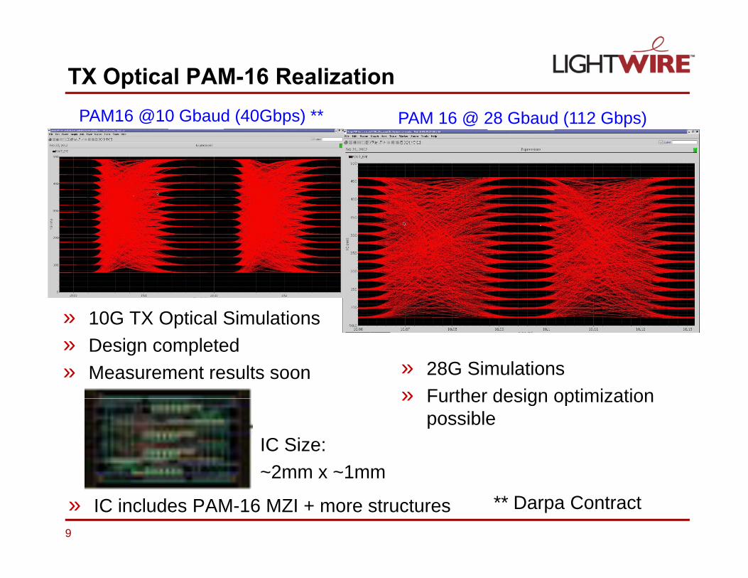
PAM-16 optical eyeTX Optical PAM-16 Realization
PAM 16 @ 28 Gbaud (112 Gbps)PAM16 @10 Gbaud (40Gbps) **
» 10G TX Optical Simulations
» 28G Simulations» Further design optimization
p» Design completed» Measurement results soon
» Further design optimization possible
IC Size: ~2mm x ~1mm
9
** Darpa Contract~2mm x ~1mm
» IC includes PAM-16 MZI + more structures

Summary
» SiPhotonics enable very efficient implementation of Multi-level modulation
» Excellent correlation between simulation and measurements
Hi h d d l ti i CMOS h t i h» High speed modulation using CMOS photonics shown• Required rise time / fall time performance demonstrated
» Simulation show 100G PAM-16 optical modulation realizable using current technology
» 40G PAM-16 optical modulation silicon measurement results soon
10

Additional Reference Slides
11

What is CMOS Photonics?CMOS Photonics Introduction
CMOS IC Platform
DC El t DC Ph t
CMOS Photonics IC Platform
DC Electron Supply
DC Electron Supply
DC Photon Supply
Electronic ICmanipulates electrons Electrical I/O
Optical I/OOpto-Electronic ICmanipulates both photons
d l t iusing transistorsElectrical I/O
and electrons using transistors
CMOS Photonics IC Platform leverages existing multi-billion dollars of investment, I f t t d di i li f th CMOS IC i d t t i l t b th El t
12
Infra-structure and discipline of the CMOS IC industry to manipulate both Electrons & Photons to achieve desired Opto-Electronics functions using External DC Sources

Fundamental Technology
MOS Transistor
G a te
CMOS Photonics ModulatorV+
S o u rc e D ra in
Drain
D iS u b s tr a te
V-
Drain
By controlling the voltages on terminals, MOS
Transistor controls the flow of electrons
from source to drain. Today, 100s of millions
can be placed on a single electronics chip
By controlling the voltages of the two arms of the modulator, one controls the flow of photons from source to drain with one major difference – Photons cannot be stopped and hence the unwanted will go
can be placed on a single electronics chip.
f C
to Drain. A large numbers of these can be integrated on a single chip.
13
Just like the transistor is the basic building block for all ICs, Broadband Modulator is the basic building block for all high speed optical interconnects

Mach Zehnder Interferometer (MZI)Modulator overview
Left armVleft+
-
Right armVright+
-
Optical Power
POUT
2OMA
» Control left and right arms to be in phase (optical 1) and out of phase ( ti l 0) b l i lt th l th f th MZI
ΘR - ΘL
0 Π
(optical 0) by applying voltage across the length of the MZI
» Phase v/s output optical power in raised cosine relationship
14
» VπLπ = Measure of voltage and length required to get full π phase shiftMZI deployed in optical systems for over 20 years

Lightwire’s MZI
» VπLπ < 2 Vmm
» What does this mean?
• Between two arms we need < 1Vmm
• Enables smaller length modulators (in 100s of microns)
• Enables cmos compatible drive voltages (< ~1V)
• Implemented in CMOS process
» Uses CW (DC) lasers rather than direct modulation
15
CMOS photonics enables small size, low power MZI modulators