high speed layout guidelines - texas instruments
TRANSCRIPT

Application ReportSCAA082–November 2006
High-Speed Layout GuidelinesAlexander Weiler and Alexander Pakosta ............................................................................ Clock Drivers
ABSTRACT
This application report addresses high-speed signals such as clock signals and theirrouting and gives designers a review of the important coherences. With some simplerules, electromagnetic interference problems can be minimized without usingcomplicated formulas and expensive simulation tools. Section 1 gives a shortintroduction to theory; section 2 focuses on practical PCB design rules. Either sectioncan be read independently.
Contents1 Theoretical Overview............................................................................... 2
1.1 Electromagnetic Interference and Electromagnetic Compatibility ................... 21.2 Clock Signals............................................................................... 21.3 Transmission Lines........................................................................ 31.4 Crosstalk .................................................................................... 81.5 Differential Signals......................................................................... 81.6 Return Current and Loop Areas ......................................................... 8
2 Practical PCB Design Rules ...................................................................... 92.1 PCB Considerations During the Circuit Design........................................ 92.2 Board Stackup ............................................................................. 92.3 Power and Ground Planes.............................................................. 102.4 Decoupling Capacitors .................................................................. 132.5 Traces, Vias, and Other PCB Components .......................................... 142.6 Clock Distribution......................................................................... 17
3 Summary ........................................................................................... 184 References......................................................................................... 19
List of Figures
1 Model of Electromagnetic Interference .......................................................... 22 Time Domain and Frequency Domain of a Clock Signal...................................... 33 Structure and Dimension of Microstrip and Stripline ........................................... 34 Calculation of Properties of Microstrip and Stripline (AppCAD) .............................. 55 Over- and Undershoots Due to Incorrect Termination......................................... 76 Return Current and Resulting Loop Area........................................................ 87 Loop Area and Crosstalk Due to Poor Signal Routing and Ground Splitting ............. 118 Poor and Good Placement of the Common Ground in a Split Ground Environment .... 119 Good Placement of Different Functional Blocks Without the Need of a Split Ground
Plane................................................................................................ 1210 Crosstalk Induced by the Return Current Path................................................ 1211 Impedance of Different Capacitors Over a Wide Frequency Range and the
Resulting Impedance of Their Parallel Connection ........................................... 1312 Poor and Good Placement and Routing of Bypass Capacitors............................. 1413 Poor and Good Right Angle Bends ............................................................. 1414 Loop Areas Caused by Poor Via Placement .................................................. 1515 Poor and Good Via Placement .................................................................. 16
SCAA082–November 2006 High-Speed Layout Guidelines 1Submit Documentation Feedback
www.ti.com
1 Theoretical Overview
1.1 Electromagnetic Interference and Electromagnetic Compatibility
Sink
Source Sink
Source
Coupling Path
1.2 Clock Signals
Theoretical Overview
16 Reflection Caused by Stubs in a Via ........................................................... 1717 Poor and Good Clock Distribution on a PCB .................................................. 18
List of Tables
1 Description of the Symbols Used in Figures 3 and 4 .......................................... 42 Comparison of Propagation Delay Time......................................................... 63 Possible Board Stackup on a Four-Layer PCB ................................................. 94 Possible Board Stackup on a Six-Layer PCB ................................................. 10
Some basic understanding is desirable in order to effectively use the PCB design rules given in thisdocument. Then, it is easy to identify the undesirable effects that can arise and how to avoid them. Thereason PCB layout becomes more and more important is because of the trend to faster, higher integrated,smaller form factors and lower power electronic circuits. The higher the switching frequencies are, themore radiation occurs on a PCB. With good layout, many EMI problems can be minimized in order to meetrequired specifications.
Electromagnetic interference (EMI) is radio frequency energy that interferes with the operation of anelectronic device. This radio frequency energy can be produced by the device itself or by other devicesnearby.
Electromagnetic compatibility (EMC) is the ability of an electronic product to operate without causing EMIthat would interfere with other equipment and without being affected by EMI from other equipment or theenvironment.
The goal is to reduce EMI to meet the requirements given by the Federal Communication Commission(FCC) or the International Special Committee on Radio Interference (CISPR)
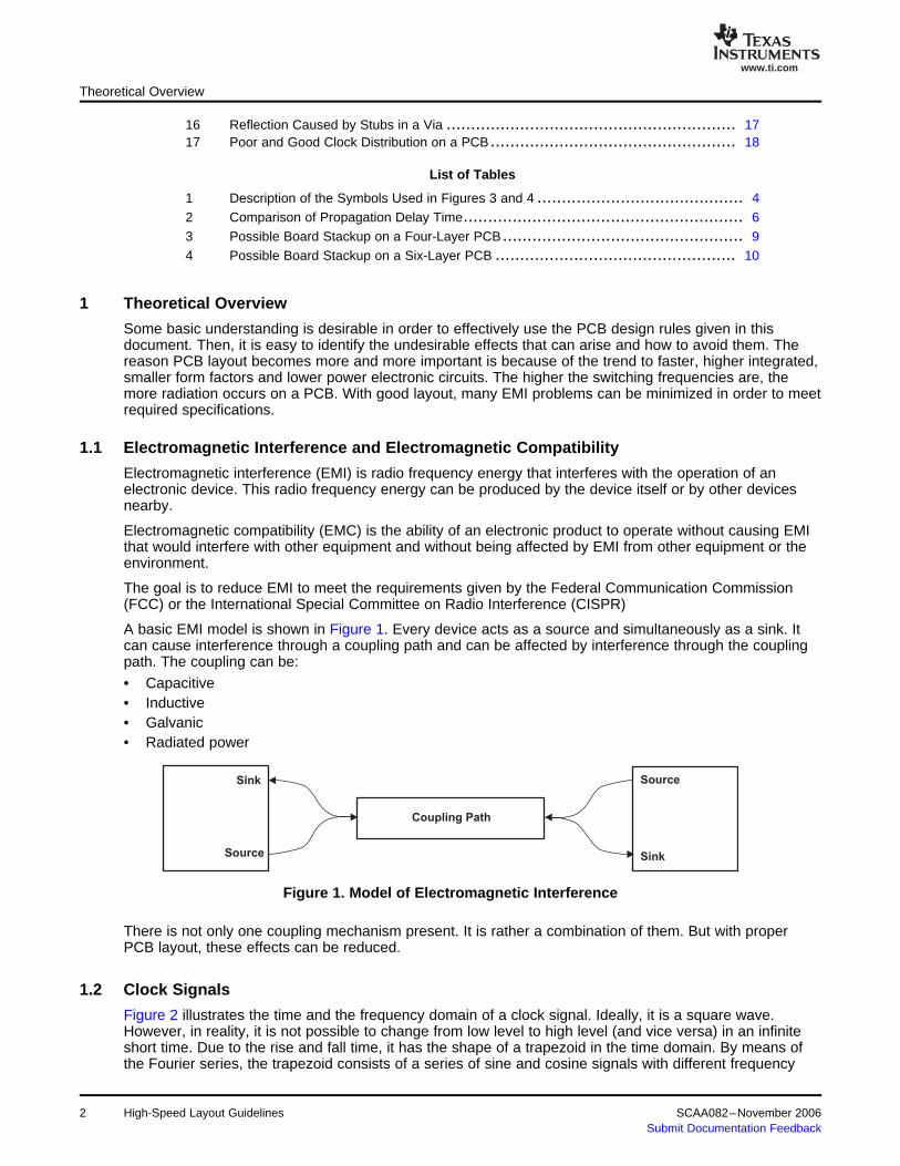
A basic EMI model is shown in Figure 1. Every device acts as a source and simultaneously as a sink. Itcan cause interference through a coupling path and can be affected by interference through the couplingpath. The coupling can be:
• Capacitive• Inductive• Galvanic• Radiated power
Figure 1. Model of Electromagnetic Interference
There is not only one coupling mechanism present. It is rather a combination of them. But with properPCB layout, these effects can be reduced.
Figure 2 illustrates the time and the frequency domain of a clock signal. Ideally, it is a square wave.However, in reality, it is not possible to change from low level to high level (and vice versa) in an infiniteshort time. Due to the rise and fall time, it has the shape of a trapezoid in the time domain. By means ofthe Fourier series, the trapezoid consists of a series of sine and cosine signals with different frequency
2 High-Speed Layout Guidelines SCAA082–November 2006Submit Documentation Feedback

www.ti.com
1.3 Transmission Lines
Theoretical Overview
and magnitude. The discrete frequency components have an envelope as is shown in the lower diagramof Figure 2. An important aspect is that in the frequency domain the amplitude of the higher frequencyharmonics depends on the rise and fall time of the signal. The longer the rise time, the smaller themagnitude of the harmonics. For example, the harmonics of a 100-MHz clock signal are not negligible,especially the third and fifth. In this case, consideration also should be made with frequencies up to 500MHz. With CDCE906 from Texas Instruments, the user can set different rise and fall times to reduce theamplitude of the harmonics. However, care must be taken that these times do not violate the slew ratespecifications of the driven devices.
Figure 2. Time Domain and Frequency Domain of a Clock Signal
If the lengths of traces are in the range of the signal's wavelength, then the user has to consider theeffects of transmission lines. The problems that a user must deal with are time delay, reflections, andcrosstalk. To get a better understanding of these problems and where and how they arise, it is useful toknow what transmission lines are. They are simply the traces on a PCB and depend on the length and thefrequency of the signals passing through them.
Many different structures of trace routing are possible on a PCB. Two common structures are shown inFigure 3. On the left, a microstrip structure is illustrated and on the right, a stripline technique. A microstriphas one reference, often a ground plane, and these are separated by a dielectric. A stripline has tworeferences, often multiple ground planes, and are surrounded with the dielectric.
Figure 3. Structure and Dimension of Microstrip and Stripline
The following sections describe some important properties of transmission lines which are significant forPCB design. Many software tools are available to calculate the properties of the several transmission line
SCAA082–November 2006 High-Speed Layout Guidelines 3Submit Documentation Feedback

www.ti.com
3 108 ms
eff ƒ
Theoretical Overview
structures. In this application report, the freeware AppCAD from Agilent is used so that the reader canbecome familiar with these properties. Figure 4 shows the two structures, microstrip (top) and stripline(bottom). The dimensions, the material, and the frequency are in each case shown on the left. The resultsthat are used in the following sections can be seen on the right. Table 1 defines the symbols used inFigure 3 and Figure 4.
Table 1. Description of the Symbols Used in Figures 3 and 4
SYMBOL DESCRIPTION
H Height of the dielectric
W Width of the trace
L Length of the trace
Frequency The frequency on which the calculations are based
Z0 Characteristic impedance of the trace
1.0 Wavelength Wavelength λ of the trace at the given frequency and the given effective dielectric
VP Velocity of the signal on this trace with the given dimensions and frequency relative to the speed of light. Theabsolute velocity is calculated by VP,.absolute = VP,.relative × 3 × 10⁸ m/s
εeff Combination of the several dielectrics which surrounds the microstrip
W/H Ratio between trace width and trace length
High-Speed Layout Guidelines4 SCAA082–November 2006Submit Documentation Feedback

www.ti.com
Theoretical Overview
Figure 4. Calculation of Properties of Microstrip and Stripline (AppCAD)
SCAA082–November 2006 High-Speed Layout Guidelines 5Submit Documentation Feedback
www.ti.com
(1) Pd is the propagation delay time in ps on the mentioned line with A 100-mm length. Pd 1171.9 mmns
100 mm
1.3.1 Signal Speed and Propagation Delay Time
V 3 108 ms
r
(1)
1.3.1.1 Examples
1.3.2 Characteristic Impedance, Reflections, and Termination
calculated as
R Z0R Z0
.For the two mentioned cases, the reflection coefficient becomes ρ = +1 for an
Theoretical Overview
A signal cannot pass through a trace with infinite speed. The maximum speed is the speed of light with 3 ×10⁸ m/s. For a certain trace length, the signal needs a certain time to pass it, and this is called thepropagation delay time. The standard medium for the speed of light is air. For another medium, thedielectric in a PCB environment, the speed is different than that of the speed of light in air. The formula forthe speed on a stripline is:
So, the speed is a function of the dielectric which surrounds the trace. For a microstrip, it is morecomplicated because the trace is not surrounded by one dielectric. There are at least two: the substrateunder the trace and the air above the trace. If the PCB contains a solder mask, a third medium would bepresent. Therefore, the calculation of an effective εr is necessary before determining the signal speed. Itdepends on the width of the microstrip and the distance to the reference plane. In this case, the speed is afunction of the present dielectric, the trace width, and its distance to the reference plane [12].
The signal speed and the propagation delay time, respectively, on a signal trace are important when:
• Timing and skew requirements need to be met (clock distribution, buses, etc)• Differential traces were used (e.g., LVDS)
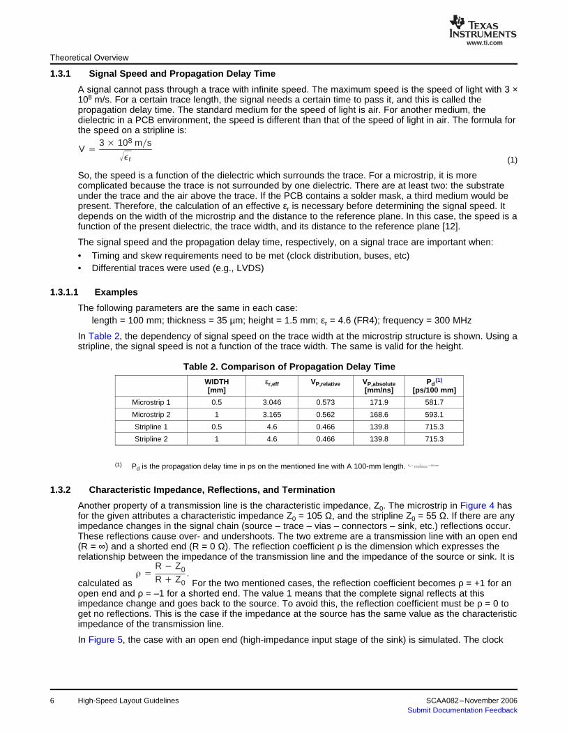
The following parameters are the same in each case:length = 100 mm; thickness = 35 µm; height = 1.5 mm; εr = 4.6 (FR4); frequency = 300 MHz
In Table 2, the dependency of signal speed on the trace width at the microstrip structure is shown. Using astripline, the signal speed is not a function of the trace width. The same is valid for the height.
Table 2. Comparison of Propagation Delay Time
WIDTH εr,eff VP,relative VP,absolute Pd(1)
[mm] [mm/ns] [ps/100 mm]
Microstrip 1 0.5 3.046 0.573 171.9 581.7
Microstrip 2 1 3.165 0.562 168.6 593.1
Stripline 1 0.5 4.6 0.466 139.8 715.3
Stripline 2 1 4.6 0.466 139.8 715.3
Another property of a transmission line is the characteristic impedance, Z0. The microstrip in Figure 4 hasfor the given attributes a characteristic impedance Z0 = 105 Ω, and the stripline Z0 = 55 Ω. If there are anyimpedance changes in the signal chain (source – trace – vias – connectors – sink, etc.) reflections occur.These reflections cause over- and undershoots. The two extreme are a transmission line with an open end(R = ∞) and a shorted end (R = 0 Ω). The reflection coefficient ρ is the dimension which expresses therelationship between the impedance of the transmission line and the impedance of the source or sink. It is
open end and ρ = –1 for a shorted end. The value 1 means that the complete signal reflects at thisimpedance change and goes back to the source. To avoid this, the reflection coefficient must be ρ = 0 toget no reflections. This is the case if the impedance at the source has the same value as the characteristicimpedance of the transmission line.
In Figure 5, the case with an open end (high-impedance input stage of the sink) is simulated. The clock
6 High-Speed Layout Guidelines SCAA082–November 2006Submit Documentation Feedback

www.ti.com
Theoretical Overview
source has an output of 3.3 V and an impedance of 25 Ω. The red line (dotted) is the ideal shape of theclock output. The green one (dashed) is the real signal at the clock's output and the blue line is at the endof the transmission line. The reflection is the cause of these over- and undershoots. The maximum voltageat the trace end is approximately 4.4 V instead of 3.3 V, and the minimum voltage is approximately –1 Vinstead of 0 V. These circumstances can damage the input stage of the source and sink.
Figure 5. Over- and Undershoots Due to Incorrect Termination
A receiver often has a high-impedance input. To avoid these over- and undershoots, the reflections mustbe reduced. Therefore, a proper termination is required. The most common termination techniques follow:
• Series termination• Parallel termination• Thevenin termination• AC termination
Each of them has advantages and disadvantages, and the designer has to trade off which one is the bestsolution for his design.
SCAA082–November 2006 High-Speed Layout Guidelines 7Submit Documentation Feedback

www.ti.com
1.4 Crosstalk
1.5 Differential Signals
1.6 Return Current and Loop Areas
Theoretical Overview
References: [8], [9]
The mutual influence of two parallel, nearby routed traces is called crosstalk. One is called the aggressor(this trace carries the signal) and the other is called the victim (this trace is influenced by the aggressor).Due to the electromagnetic field, the victim is influenced by an inductive and a capacitive coupling. Theygenerate a forward and a backward current in the victim trace whereas in a homogenous environment(e.g., stripline) the two induced currents cancel each other. In a microstrip environment, the forwardcurrent of the inductive coupling tends to be larger than the influence of the capacitive coupling. Tominimize the effects on crosstalk on adjacent traces, keep them at least 2 times the trace width apart.
References: [1], [2], [3], [4], [5]
In the case of differential signals, the negative effect of crosstalk is a positive one. The signals on eachtrace are in theory exactly equal in magnitude and opposite in their sign. So, their electromagnetic fieldscancel each other and the return current on the ground plane, as well. To achieve this, the traces for bothsignals must have the same length in order that the propagation delay times are equal. The receiver issensitive to the differences of the signals and not to an absolutely level reference, e.g., to ground. If anysignal radiated equally into both differential traces, the receiver would not recognize it. Therefore, thedesigner has to make sure that radiation affects both traces equally. This can be realized by routing thedifferential traces as close as possible.
References: [1], [6], [7]
An electrical circuit must always be a closed loop. Up to now, only the signal path was discussed but notthe path back to the source – the return current. With DC, the return current takes the way back with thelowest resistance (Figure 6a). With a higher frequency, the return current flows along the lowestimpedance (Figure 6b). This is directly beside the signal.
Figure 6. Return Current and Resulting Loop Area
If this return path, mostly the ground plane, has a slot, the return current has to take another way and thisresults in a loop area (Figure 6c). The larger the area, the more radiation and EMI problems occur. Thedesigner has to make sure that the return current can flow directly underneath the signal trace. Onesolution is to place a 0-Ω resistor over the slot (Figure 6d). Another is to route the signal the same way asthe return current flows. The best solution is to avoid any slots in the ground reference plane.
High-Speed Layout Guidelines8 SCAA082–November 2006Submit Documentation Feedback

www.ti.com
2 Practical PCB Design Rules
2.1 PCB Considerations During the Circuit Design
2.2 Board Stackup
Practical PCB Design Rules
Because many things can affect transmission lines, EMI problems can occur. In order to reduce theseproblems, good PCB design is important and with some simple design rules, the PCB designer canminimize these problems. It is important to make prudent decisions during new circuit design, like theminimum number of layers. The easiest way to get a good, new design is to copy the recommendeddesign from the TI evaluation modules (EVM).
A good PCB layout starts with the circuit design. Do not postpone considerations about the layout. One ofthe most important aspects affecting the layout is the location of each functional block. Keep their devicesand their traces together.
• What is the highest frequency and fastest rise time in the system?• What are the electrical specifications at the inputs and outputs of the sinks and sources?• Are there sensitive signals to route – for example, think about controlled impedance, termination,
propagation delay on a trace (clock distribution, buses, etc.)?• Is a microstrip adequate for the sensitive signals, or is it essential to use stripline technique?• How many different supply voltages exist? Does each supply voltage need its own power plane, or is it
possible to split them?• Create a diagram with the functional groups of the system – e.g., transmitter path, receiver path,
analog signals, digital signals, etc.• Are there any interconnections between at least two independent functional groups? Take special care
of them. Think about the return current and crosstalk to other traces.• Clarify the minimum width, separation and height of a trace with the PCB manufacturer. What's the
minimum distance between two layers? What about the minimum drill and the requirements of vias? Isit possible to use blind vias and buried vias?
Equipped with this information, a designer can do a lot of basic design.
There is no fundamental information about how many layers should be used and how the board stackupshould look. Again, the easiest way the get good results is to use the design from the EVMs of TexasInstruments. The magazine Elektronik Praxis [11] has published an article with an analysis of differentboard stackups. These are listed in Table 3 and Table 4.
Generally, the use of microstrip traces needs at least two layers, whereas one of them must be a GNDplane. Better is the use of a four-layer PCB, with a GND and a VCC plane and two signal layers. If thecircuit is complex and signals must be routed as stripline, because of propagation delay and/orcharacteristic impedance, a six-layer stackup should be used.
Table 3. Possible Board Stackup on a Four-Layer PCB
Model 1 Model 2 Model 3 Model 4
Layer 1 SIG SIG SIG GND
Layer 2 SIG GND GND SIG
Layer 3 VCC VCC SIG VCC
Layer 4 GND SIG VCC SIG
Decoupling Good Good Bad Bad
EMC Bad Bad Bad Bad
Signal integrity Bad Bad Good Bad
Self disturbance Satisfaction Satisfaction Satisfaction High
SCAA082–November 2006 High-Speed Layout Guidelines 9Submit Documentation Feedback

www.ti.com
2.3 Power and Ground Planes
Practical PCB Design Rules
Table 4. Possible Board Stackup on a Six-Layer PCB
Model 1 Model 2 Model 3 Model 4 Model 5 Model 6
Layer 1 SIG SIG GND SIG SIG SIG
Layer 2 SIG GND VCC GND GND GND
Layer 3 VCC VCC SIG VCC VCC VCC
Layer 4 GND VCC SIG SIG GND GND
Layer 5 SIG GND VCC GND Not used SIG
Layer 6 SIG SIG GND SIG SIG SIG
Decoupling Good Good Good Good Good Good
EMC Bad Good Satisfaction Satisfaction Good Good
Signal integrity Bad Good Bad Good Good Bad
To determine the right board stackup, consider the following points:
• Define the location of each section on the board by means of the functional diagram. Try to keep thedevices together to avoid interaction (crosstalk, influence of noise) between two separate blocks (liketransmitter–receiver or analog–digital).
• At which functional block is which supply voltage used?• It is necessary in high-speed designs to have at least one complete ground plane as a reference for
microstrip traces for sensitive signals.• With a complete power plane as close as possible to the ground plane, it is possible to create
capacitive coupling between them to get low impedance at high frequencies. This reduces the amounton small decoupling capacitors at the power pins of the devices. The closer the planes, the lessimpedance is present [13].
As previously mentioned, a complete ground plane in high-speed design is essential. Additionally, acomplete power plane is recommended as well. In a complex system, several regulated voltages can bepresent. The best solution is for every voltage to have its own layer and its own ground plane. But thiswould result in a huge number of layers just for ground and supply voltages. What are the alternatives?Split the ground planes and the power planes? In a mixed-signal design, e.g., using data converters, themanufacturer often recommends splitting the analog ground and the digital ground to avoid noise couplingbetween the digital part and the sensitive analog part.
Take care when using split ground planes because:
• Split ground planes act as slot antennas and radiate.• A routed trace over a gap creates large loop areas, because the return current cannot flow beside the
signal, and the signal can induce noise into the nonrelated reference plane (Figure 7).• With a proper signal routing, crosstalk also can arise in the return current path due to discontinuities in
the ground plane. Always take care of the return current (Figure 10).
Figure 7: Do not route a signal referenced to digital ground over analog ground and vice versa. The returncurrent cannot take the direct way along the signal trace and so a loop area occurs. Furthermore, thesignal induces noise, due to crosstalk (dotted red line) into the analog ground plane.
10 High-Speed Layout Guidelines SCAA082–November 2006Submit Documentation Feedback

www.ti.com
Practical PCB Design Rules
Figure 7. Loop Area and Crosstalk Due to Poor Signal Routing and Ground Splitting
Figure 8: Do not let one ground plane pass another ground plane to get connected to the common ground(a). Every ground plane must have its own path to the common ground to reduce noise (b).
Figure 8. Poor and Good Placement of the Common Ground in a Split Ground Environment
Figure 9: The use of a complete ground plane is a better solution. Place the devices by function and routetheir signals only in their region. If any interconnection between analog and digital occurs, be careful withcrosstalk and the return current path.
SCAA082–November 2006 High-Speed Layout Guidelines 11Submit Documentation Feedback

www.ti.com
Practical PCB Design Rules
Figure 9. Good Placement of Different Functional Blocks Without the Need of a Split Ground Plane
Figure 10: If the trace routing of two signals is done properly, it is still possible to induce noise in the returncurrent path by means of crosstalk. In this case, a loop area and crosstalk in the return current path havebeen created.
• If possible, use a continuous ground plane; do not split them. This can be achieved by a properplacement selection. Again, create functional blocks, and place and route them together. By doing this,the traces of a digital part cannot influence any trace of the analog part if these sections do not crosseach other.
If split ground planes are essential:
• Do not route signals over a gap. Always strive for the return current flow with the smallest loop area.• Connect split ground planes only at one point. More common ground connections can create ground
loops, and this increases radiation.• The return current of a subsystem (e.g., an analog system or transmitter path) must not be in the path
of the other subsystem (digital system or receiver path). The return current should flow directly to thecommon ground point (Figure 8).
• Power planes should only reference their own ground plane. They should not overlap with anotherground plane. This leads to capacitive coupling between the power plane and a not-referenced groundplane. Noise can couple into the other system.
• Do not connect bypass capacitors between a power plane and an unrelated ground plane. Again,noise can be coupled from one supply system into the other. This mistake can occur in the circuitdesign section.
Figure 10. Crosstalk Induced by the Return Current Path
High-Speed Layout Guidelines12 SCAA082–November 2006Submit Documentation Feedback

www.ti.com
2.4 Decoupling Capacitors
Practical PCB Design Rules
Decoupling capacitors between the power pin and ground pin of the device ensure low ac impedance toreduce noise and to store energy. To reach low impedance over a wide frequency range, severalcapacitors must be used. This is why, a real capacitor consists of its capacitance and a parasiticinductance and resistance. Therefore, every real capacitor behaves as a resonant circuit. The capacitivecharacteristics are only valid up to its self-resonant frequency (SRF). Above the SRF, the parasitic effectsdominate, and the capacitor acts as an inductor. With the use of several capacitors with different values,low ac impedance over a wide frequency range can be provided.
Figure 11. Impedance of Different Capacitors Over a Wide Frequency Range and the ResultingImpedance of Their Parallel Connection
Figure 11 shows this context. Capacitors with high values have low impedance in the lower frequencyrange and a low SRF, whereas small-valued capacitors have their SRF in the upper frequency range. Thisdepends on the equivalent series resistance (ESR) and the equivalent series inductance (ESL). A goodcombination of several capacitors leads to a low impedance over a wide frequency range. This is shownwith the Cparallel curve in Figure 11. The gap (increase of the impedance) at around 60 MHz is the resultof a missing capacitance. If there were a value between 100 nF and 10 nF, the Cparallel curve would notincrease.
As previously mentioned, a power and GND plane can represent a capacitance that ensures lowimpedance at high frequencies. Therefore, a well-designed board stackup can minimize the number ofcapacitors required having low-capacitance values.
General rules for placing capacitors:
• Place the lowest valued capacitor as close as possible to the device to minimize the inductive influenceof the trace. This is especially important for small capacitor values, because the inductive influence ofthe trace is not negligible anymore.
• Place the lowest valued capacitor as close as possible to the power pin/power trace of the device.• Connect the pad of the capacitor directly with a via to the ground plane. Use two or three vias to get a
low-impedance connection to ground. If the distance to the ground pin of the device is short enough,you can connect it directly.
• Make sure that the signal must flow along the capacitor.
SCAA082–November 2006 High-Speed Layout Guidelines 13Submit Documentation Feedback

www.ti.com
Poor Bypassing
Good Bypassing
2.5 Traces, Vias, and Other PCB Components
Practical PCB Design Rules
Figure 12. Poor and Good Placement and Routing of Bypass Capacitors
A right angle in a trace can cause more radiation. The capacitance increases in the region of the corner,and the characteristic impedance changes. This impedance change causes reflections.
• Avoid right-angle bends in a trace and try to route them at least with two 45° corners. To minimize anyimpedance change, the best routing would be a round bend (see Figure 13).
• Separate high-speed signals (e.g., clock signals) from low-speed signals and digital from analogsignals; again, placement is important.
• To minimize crosstalk not only between two signals on one layer but also between adjacent layers,route them with 90° to each other.
Figure 13. Poor and Good Right Angle Bends
The use of vias is essential in most routings. But the designer has to be careful when using them. Theyadd additional inductance and capacitance, and reflections occur due to the change in the characteristicimpedance. Vias also increase the trace length.
• Avoid vias in differential traces. If it is impossible to avoid them, use vias in both traces or compensatethe delay also in the other trace.
14 High-Speed Layout Guidelines SCAA082–November 2006Submit Documentation Feedback

www.ti.com
Practical PCB Design Rules
Figure 14. Loop Areas Caused by Poor Via Placement
Figure 14 illustrates another problem with vias – loop areas. The designer has to make sure that thereturn current can flow ideally underneath (beside) the signal trace. A good way to realize this is to addsome ground vias around the signal via. This is a similar structure to a coaxial line. Care must be taken, ifthe new layer has another distance to the reference plane. This can cause reflections due to animpedance change.
Figure 15 shows, how good via placement avoids loop areas, if there is need for multiple vias.
SCAA082–November 2006 High-Speed Layout Guidelines 15Submit Documentation Feedback

www.ti.com
Practical PCB Design Rules
Figure 15. Poor and Good Via Placement
Figure 15: Because of wrong via placement, especially with bus signals, slots in the ground plane canarise. Further, the return current can create a loop area when placing the vias in the wrong direction.Three different routings are shown on the left. On the right, some traces are masked out to see how thereturn current (green trace) will flow.
In Figure 16, a four-layer stackup can be seen. The signal changes from layer 1 to layer 2. The via passesthrough all four layers. Thus, we get the structure of an open-end transmission line with no termination
16 High-Speed Layout Guidelines SCAA082–November 2006Submit Documentation Feedback

www.ti.com
2.6 Clock Distribution
Practical PCB Design Rules
and thereby a 100% reflection. Due to the length of the stub, a delay also occurs. The worst case is nowthat the two signals (original one → red and reflected one → gray) on layer 2 have a phase shift of 180°,and so they cancel each other. The phase shift is due to the delay which arises from the stub length. Thetime delay is twice the stub length divided by the signal speed. To avoid this problem, use blind vias orburied vias.
Figure 16. Reflection Caused by Stubs in a Via
Tips for routing traces and the use of vias:
• Do not use right-angle bends on traces with controlled impedance and fast rise time, respectively.• Route the traces orthogonally to each other on adjacent layers to avoid coupling.• To minimize crosstalk, the distance between two traces should be approximately 2 to 3 times the width
of the trace.• Differential traces should be routed as close as possible to get a high coupling factor. As a result of
this, influenced noise is then a common-mode noise and is not a problem for a differential input stage.• Do not use vias on traces with sensitive signals, if unnecessary.• Be careful with the return current when changing the layers. Use ground vias around the signal via to
make sure that the return current can flow as close as possible to the signal (Figure 14).• Do not create slots, for example in the ground plane, by using closely placed vias (Figure 15).• Consider stubs created by vias. If necessary, use blind vias or buried vias (Figure 16).
Figure 17 shows four possible clock distribution circuits. The problems in Figure 17a are the enormousreflections at the branches and the different trace length to the devices. Because of the delay, it ispossible that the system cannot function properly. To avoid the reflection at the branches, do not use them(Figure 17b). Route the signal in a chain from one device to the other and realize a proper termination. Becareful with the delay. In a high-speed environment, it is possible that the data, sent from device A todevice B, is out of date when the clock signal arrives at device B. A star connection as shown inFigure 17c is a good solution to minimize the delay. A clock driver is used to distribute the clock signals tothe different devices. To minimize the skew, the same trace length for every clock signal should be used.Figure 17d illustrates a solution for a complex system. A main clock feeds several clock drivers. Again, toreach low skew, implement delay-time compensation and use a proper termination to avoid reflections.
• Be careful with trace length in a clock distribution layout. Consider the delay for each trace. The bestsolution is to route these signals with the same length.
• Avoid branches to reduce reflections. Use a clock driver to distribute the signal to every device andconsider a proper termination.
SCAA082–November 2006 High-Speed Layout Guidelines 17Submit Documentation Feedback

www.ti.com
ClockDriver
ClockDriver
ClockDriver
ClockDriver
ClockGenerator
Matching ofLine Length
ImpedanceMatching
ClockDriver
Clocka) c)
d)
data-line
ClockDriver
b)Clock
1 nF
100 W
A
B
3 Summary
Summary
Figure 17. Poor and Good Clock Distribution on a PCB
This document presents an introduction to designing a PCB, a complex topic. However, the rulespresented in this introduction can assist the designer in creating proper PCB designs. The higher thesignal frequency with which the designer must contend, the more complicated will be the PCB design.Complicated PCB designs require a deep knowledge, experience, and simulation tools. However, it is notalways necessary to route traces as short as possible, differential signals as close as possible, or to avoidcrosstalk as much as possible. Rather, it depends on the signal on the trace. Basically, the designer mustknow which are the sensitive parts in the circuit or where problems due to reflections can occur. With thisknowledge, a good placement of the devices can be made. Because placement is such an important stepin high-speed design, the designer will do well to always keep it and the return current in mind.
High-Speed Layout Guidelines18 SCAA082–November 2006Submit Documentation Feedback

www.ti.com
4 References
References
1. High-Speed DSP Systems Design – Reference Guide (SPRU889)2. Crosstalk, Part 1: The conversion we wish would stop, Douglas Brooks,
http://www.ultracad.com/articles/crosstlk.pdf3. Crosstalk, Part 2: How loud is your crosstalk?, Douglas Brooks,
http://www.ultracad.com/articles/crosstlk.pdf4. Crosstalk, EMI and differential Z, Douglas Brooks,
http://www.ultracad.com/articles/crossemianddifferentialz.pdf5. Crosstalk, Part 1: Understanding Forward vs Backward, Douglas Brooks,
http://www.ultracad.com/mentor/mentor%20crosstalk%20part1.pdf6. Differential Impedance: What's the difference, Douglas Brooks,
http://www.ultracad.com/articles/diff_z.pdf7. Differential Signals, Douglas Brooks, http://www.ultracad.com/articles/differentialrules.pdf8. Adjusting signal timing (part 1), Douglas Brooks,
http://www.ultracad.com/mentor/mentor%20signal%20timing1.pdf9. Transmission line termination, Douglas Brooks,
http://www.ultracad.com/mentor/transmission%20line%20terminations.pdf10. EMV-Design Richtlinien, B.Foeste/s.Oeing, ISBN: 3-7723-5499-8, Franzis11. Elektronik-Praxis: Die Leiterplatte 2010, Ausgabe 11/06, P72-7712. Microstrip propagation times – slower than we think, Douglas Brooks,
http://www.ultracad.com/mentor/microstrip%20propagation.pdf13. Design for minimizing electromagnetic interference in high frequency RF and digital boards and
systems, Dr. Eric Bogatin, www.bethesignal.com
SCAA082–November 2006 High-Speed Layout Guidelines 19Submit Documentation Feedback

IMPORTANT NOTICE
Texas Instruments Incorporated and its subsidiaries (TI) reserve the right to make corrections, modifications,enhancements, improvements, and other changes to its products and services at any time and to discontinueany product or service without notice. Customers should obtain the latest relevant information before placingorders and should verify that such information is current and complete. All products are sold subject to TI’s termsand conditions of sale supplied at the time of order acknowledgment.
TI warrants performance of its hardware products to the specifications applicable at the time of sale inaccordance with TI’s standard warranty. Testing and other quality control techniques are used to the extent TIdeems necessary to support this warranty. Except where mandated by government requirements, testing of allparameters of each product is not necessarily performed.
TI assumes no liability for applications assistance or customer product design. Customers are responsible fortheir products and applications using TI components. To minimize the risks associated with customer productsand applications, customers should provide adequate design and operating safeguards.
TI does not warrant or represent that any license, either express or implied, is granted under any TI patent right,copyright, mask work right, or other TI intellectual property right relating to any combination, machine, or processin which TI products or services are used. Information published by TI regarding third-party products or servicesdoes not constitute a license from TI to use such products or services or a warranty or endorsement thereof.Use of such information may require a license from a third party under the patents or other intellectual propertyof the third party, or a license from TI under the patents or other intellectual property of TI.
Reproduction of information in TI data books or data sheets is permissible only if reproduction is withoutalteration and is accompanied by all associated warranties, conditions, limitations, and notices. Reproductionof this information with alteration is an unfair and deceptive business practice. TI is not responsible or liable forsuch altered documentation.
Resale of TI products or services with statements different from or beyond the parameters stated by TI for thatproduct or service voids all express and any implied warranties for the associated TI product or service andis an unfair and deceptive business practice. TI is not responsible or liable for any such statements.
Following are URLs where you can obtain information on other Texas Instruments products and applicationsolutions:
Products Applications
Amplifiers amplifier.ti.com Audio www.ti.com/audio
Data Converters dataconverter.ti.com Automotive www.ti.com/automotive
DSP dsp.ti.com Broadband www.ti.com/broadband
Interface interface.ti.com Digital Control www.ti.com/digitalcontrol
Logic logic.ti.com Military www.ti.com/military
Power Mgmt power.ti.com Optical Networking www.ti.com/opticalnetwork
Microcontrollers microcontroller.ti.com Security www.ti.com/security
Low Power Wireless www.ti.com/lpw Telephony www.ti.com/telephony
Video & Imaging www.ti.com/video
Wireless www.ti.com/wireless
Mailing Address: Texas Instruments
Post Office Box 655303 Dallas, Texas 75265
Copyright 2006, Texas Instruments Incorporated