high speed 0.8mm pitch board to board connectors fx18 series
TRANSCRIPT

© 2014, HIROSE ELECTRIC CO., LTD. All rights reserved. OCT, 2014
High Speed 0.8mm pitch Board to Board Connectors
FFXX1188 SSeerriieess
DDeessiiggnn GGuuiiddee LLiinnee
OCT, 2014
Feb
.1.2
022
Cop
yrig
ht 2
022
HIR
OS
E E
LEC
TR
IC C
O.,
LTD
. All
Rig
hts
Res
erve
d.

FX18 Design Guide Line Revision 0.1 page - 2 - of 28
© 2014, HIROSE ELECTRIC CO., LTD. All rights reserved. OCT, 2014
- Table of Contents -
1. Preface ……………………………… 3 1-1 Purpose 1-2 Scope
2. Product information ……………………………… 4-6
2-1 Basic Specifications 2-2 Ordering Information 2-3 Connection Types & Dimension Drawings 2-4 MF Contact Structure
3. Connector Mounting ……………………………… 7-22 3-1 Absorption Area 3-2 Recommended Temperature Profile 3-3 Recommended Land Pattern 3-4 MF Contact Lead Reflow 3-5 Recommended Metal Mask Layout 3-6 Contact Mounting Status Check Criteria 3-7 Mounting of Multiple Connectors 3-8 Soldering Repair Procedure
4. Requirements ……………………………… 23-25 4-1 Requirements on Mating 4-2 Requirements on Rotating Insertion and Withdrawal (TADC4-210630) 4-3 Recommended Spacer Dimensions (Stacking Connection Type)
5. Caution ……………………………… 26-27 5-1 Use of Interposers 5-2 Allowable Clearance between the Mated Pair
Feb
.1.2
022
Cop
yrig
ht 2
022
HIR
OS
E E
LEC
TR
IC C
O.,
LTD
. All
Rig
hts
Res
erve
d.

FX18 Design Guide Line Revision 0.1 page - 3 - of 28
© 2014, HIROSE ELECTRIC CO., LTD. All rights reserved. OCT, 2014
1. Preface
1-1 Purpose The FX18 Series Instruction Manual is intended to provide information on basic features of the FX18 Series and the method of use, as well as to provide information on the method of designing products efficiently and improving the assembling process when the FX18 Series is used. Hirose expects that this Instruction Manual will significantly contribute to your product development, quality, and cost reduction of the entire system. Because this Instruction Manual intends only to provide general information, it does not restrict your design and does not guarantee results in all circumstances. If there is anything that does not conform to the description in this Instruction Manual, consult us for alternative solutions individually.
1-2 Scope This Instruction Manual provides useful information for the product using the FX18 Series. It describes the basic connector design information, recommended board dimensions, and requirements. This Instruction Manual will be revised on a continuing basis as technical and manufacturing capability is changed.
Feb
.1.2
022
Cop
yrig
ht 2
022
HIR
OS
E E
LEC
TR
IC C
O.,
LTD
. All
Rig
hts
Res
erve
d.
FX18 Design Guide Line Revision 0.1 page - 4 - of 28
© 2014, HIROSE ELECTRIC CO., LTD. All rights reserved. OCT, 2014
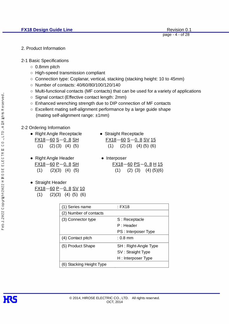
2. Product Information 2-1 Basic Specifications
○ 0.8mm pitch ○ High-speed transmission compliant ○ Connection type: Coplanar, vertical, stacking (stacking height: 10 to 45mm) ○ Number of contacts: 40/60/80/100/120/140 ○ Multi-functional contacts (MF contacts) that can be used for a variety of applications ○ Signal contact (Effective contact length: 2mm) ○ Enhanced wrenching strength due to DIP connection of MF contacts ○ Excellent mating self-alignment performance by a large guide shape
(mating self-alignment range: ±1mm)
2-2 Ordering Information ● Right Angle Receptacle ● Straight Receptacle
FX18-60 S-0 .8 SH FX18-60 S-0. 8 SV 15 (1) (2) (3) (4) (5) (1) (2) (3) (4) (5) (6)
● Right Angle Header ● Interposer
FX18-60 P-0. 8 SH FX18-60 PS-0. 8 H 15 (1) (2)(3) (4) (5) (1) (2) (3) (4) (5)(6)
● Straight Header
FX18-60 P-0. 8 SV 10 (1) (2)(3) (4) (5) (6)
(1) Series name : FX18 (2) Number of contacts (3) Connector type
S : Receptacle P : Header PS : Interposer Type
(4) Contact pitch : 0.8 mm
(5) Product Shape
SH : Right-Angle Type SV : Straight Type H : Interposer Type
(6) Stacking Height Type
Feb
.1.2
022
Cop
yrig
ht 2
022
HIR
OS
E E
LEC
TR
IC C
O.,
LTD
. All
Rig
hts
Res
erve
d.
FX18 Design Guide Line Revision 0.1 page - 5 - of 28
© 2014, HIROSE ELECTRIC CO., LTD. All rights reserved. OCT, 2014
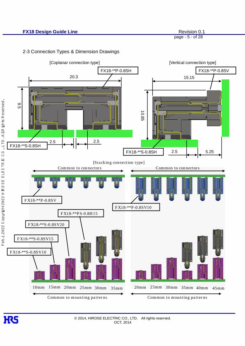
2-3 Connection Types & Dimension Drawings
15.15
10.85
2.5 5.25
[Vertical connection type]
20.3
9.5
2.5 2.5
[Coplanar connection type]
[Stacking connection type]
FX18-**P-0.8SH
FX18-**S-0.8SH
FX18-**P-0.8SV
FX18-**S-0.8SH
10mm 15mm 35mm 30mm 25mm 20mm 20mm 25mm 45mm 40mm 35mm 30mm
Common to connectors Common to connectors
Common to mounting patterns Common to mounting patterns
FX18-**P-0.8SV FX18-**P-0.8SV10
FX18-**S-0.8SV10
FX18-**S-0.8SV15
FX18-**S-0.8SV20
FX18-**PS-0.8H15
Feb
.1.2
022
Cop
yrig
ht 2
022
HIR
OS
E E
LEC
TR
IC C
O.,
LTD
. All
Rig
hts
Res
erve
d.

FX18 Design Guide Line Revision 0.1 page - 6 - of 28
© 2014, HIROSE ELECTRIC CO., LTD. All rights reserved. OCT, 2014
2-4 MF Contact Structure (Example: Coplanar Connection Type) On the guide posts on both sides of the connector, two rows of multi-functional (MF) contacts are placed for the following uses. * The vertical connection and stacking connection types also have the same product configuration. 1. Enhancing ground connection between boards 2. Using as a power line (3A/line) 3. Three-step sequence structure including signal contacts.
Note: One contact can have only one function.
Example: If an MF contact is used as a power contact, it cannot be further used as a detection contact.
[Image of three-step sequence structure] First step contact Second step contact Third step contact Mating
Grounding Signal contact Detecting (Effective mating length)
MF contact A
MF contact B
Signal contact
: Contact Header
Receptacle
0mm
(2.5mm)
(1.5mm)
(2.0mm)
2.5mm
MF contact A
2.0mm
Signal contacts
1.5mm MF contact B
Feb
.1.2
022
Cop
yrig
ht 2
022
HIR
OS
E E
LEC
TR
IC C
O.,
LTD
. All
Rig
hts
Res
erve
d.

FX18 Design Guide Line Revision 0.1 page - 7 - of 28
© 2014, HIROSE ELECTRIC CO., LTD. All rights reserved. OCT, 2014
3. Connector Mounting 3-1 Absorption Area When performing automatic mounting, see the following absorption area as reference. For the straight type, absorption tape is attached. [Right Angle Type]
[Straight Type]
10mmMAX 10mmMAX
Absorption tape length 10mmMIN
Absorption tape length 10mmMIN
Feb
.1.2
022
Cop
yrig
ht 2
022
HIR
OS
E E
LEC
TR
IC C
O.,
LTD
. All
Rig
hts
Res
erve
d.
FX18 Design Guide Line Revision 0.1 page - 8 - of 28
© 2014, HIROSE ELECTRIC CO., LTD. All rights reserved. OCT, 2014
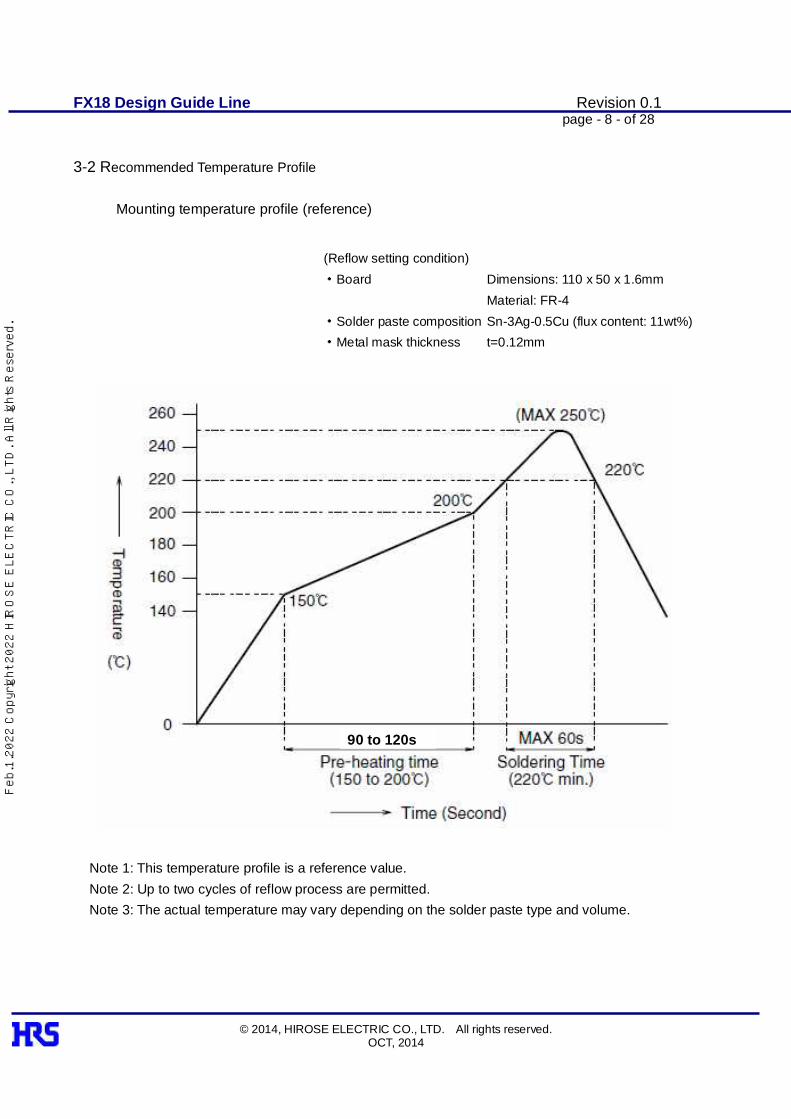
3-2 Recommended Temperature Profile
Mounting temperature profile (reference)
(Reflow setting condition) ・Board Dimensions: 110 x 50 x 1.6mm Material: FR-4 ・Solder paste composition Sn-3Ag-0.5Cu (flux content: 11wt%) ・Metal mask thickness t=0.12mm
Note 1: This temperature profile is a reference value. Note 2: Up to two cycles of reflow process are permitted. Note 3: The actual temperature may vary depending on the solder paste type and volume.
90 to 120s
Feb
.1.2
022
Cop
yrig
ht 2
022
HIR
OS
E E
LEC
TR
IC C
O.,
LTD
. All
Rig
hts
Res
erve
d.

FX18 Design Guide Line Revision 0.1 page - 9 - of 28
© 2014, HIROSE ELECTRIC CO., LTD. All rights reserved. OCT, 2014
3-3 Recommended Land Pattern Dimension of PCB (PCB Thickness:1.6mm) [FX18-**P-0. 8SH / FX18-**S-0. 8SH] [FX18-**P-0. 8SV]
No. of pos A B C 40 15.2 18.4 24.65 60 23.2 26.4 32.65 80 31.2 34.4 40.65 100 39.2 42.4 48.65 120 47.2 50.4 56.65 140 55.2 58.4 64.65
No. of pos A B C 40 15.2 18.4 24.65 60 23.2 26.4 32.65 80 31.2 34.4 40.65 100 39.2 42.4 48.65 120 47.2 50.4 56.65 140 55.2 58.4 64.65
PCB end
Dimension from PCB end
Through hole size is reduced at □ in order to stabilize the connector to PCB and prevent connector mis-position and rotation during mounting process.
Maximum allowable rotational angle of the connector after mounting by using the recommended pattern layout to be 0.2°.
MF contact A
MF contact B
MF contact A
MF contact B
Dimensions for both of MF contact A and B are symmetry with the center line.
Unit:[mm]
Unit:[mm]
Dimensions for both of MF contact A and B are symmetry with the center line.
Maximum allowable rotational angle of the connector after mounting by using the recommended pattern layout to be 0.2°.
Feb
.1.2
022
Cop
yrig
ht 2
022
HIR
OS
E E
LEC
TR
IC C
O.,
LTD
. All
Rig
hts
Res
erve
d.

FX18 Design Guide Line Revision 0.1 page - 10 - of 28
© 2014, HIROSE ELECTRIC CO., LTD. All rights reserved. OCT, 2014
[FX18-**P-0. 8SV10] [FX18-**S-0. 8SV15 / FX18-**S-0. 8SV20]
No. of pos A B C 40 15.2 18.4 24.65 60 23.2 26.4 32.65 80 31.2 34.4 40.65 100 39.2 42.4 48.65 120 47.2 50.4 56.65 140 55.2 58.4 64.65
No. of pos A B C 40 15.2 18.4 26.05 60 23.2 26.4 34.05 80 31.2 34.4 42.05 100 39.2 42.4 50.05 120 47.2 50.4 58.05 140 55.2 58.4 66.05
PCB end
MF contact A
MF contact B
Dimensions for MF contact A is line symmetry and MF contact B is point symmetry.
MF contact A
MF contact B
Unit:[mm]
PCB end
Unit:[mm]
Through hole size is reduced at □ in order to stabilize the connector to PCB and prevent connector mis-position and rotation during mounting process.
Maximum allowable rotational angle of the connector after mounting by using the recommended pattern layout to be 0.2°.
Maximum allowable rotational angle of the connector after mounting by using the recommended pattern layout to be 0.2°.
Dimensions for MF contact A is line symmetry and MF contact B is point symmetry.
Feb
.1.2
022
Cop
yrig
ht 2
022
HIR
OS
E E
LEC
TR
IC C
O.,
LTD
. All
Rig
hts
Res
erve
d.

FX18 Design Guide Line Revision 0.1 page - 11 - of 28
© 2014, HIROSE ELECTRIC CO., LTD. All rights reserved. OCT, 2014
3-4 Intrusive Reflow of MF Contacts (Stencil Design) Intrusive reflow applied to MF contacts of FX18 is that the solder paste around the through holes flows into the through holes. Please refer to this guideline prior to your stencil design. This guideline is based on our evaluation results under certain conditions, and it does not cover all the soldering and reflow conditions. Therefore, prior confirmation of solder and reflow conditions according to this guideline as reference is highly recommended. 【Intrusive Reflow Process】
①PCB
②Solder Paste Printing
Solder paste to fill in the through holes
③Place the connector onto the pattern
④Reflow
⑤Complete
Solder paste around the holes flows into each through hole.
(Printed around the holes)
Feb
.1.2
022
Cop
yrig
ht 2
022
HIR
OS
E E
LEC
TR
IC C
O.,
LTD
. All
Rig
hts
Res
erve
d.
FX18 Design Guide Line Revision 0.1 page - 12 - of 28
© 2014, HIROSE ELECTRIC CO., LTD. All rights reserved. OCT, 2014
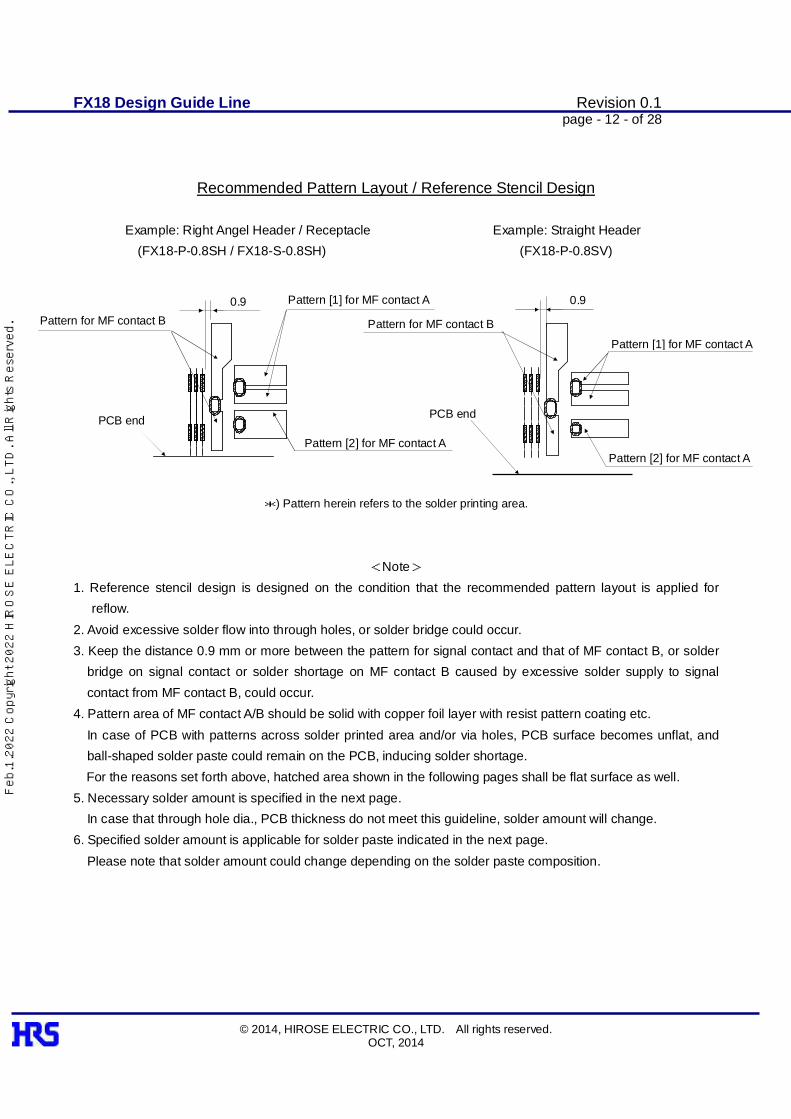
Recommended Pattern Layout / Reference Stencil Design
Example: Right Angel Header / Receptacle Example: Straight Header (FX18-P-0.8SH / FX18-S-0.8SH) (FX18-P-0.8SV)
*) Pattern herein refers to the solder printing area.
<Note> 1. Reference stencil design is designed on the condition that the recommended pattern layout is applied for
reflow. 2. Avoid excessive solder flow into through holes, or solder bridge could occur. 3. Keep the distance 0.9 mm or more between the pattern for signal contact and that of MF contact B, or solder
bridge on signal contact or solder shortage on MF contact B caused by excessive solder supply to signal contact from MF contact B, could occur.
4. Pattern area of MF contact A/B should be solid with copper foil layer with resist pattern coating etc. In case of PCB with patterns across solder printed area and/or via holes, PCB surface becomes unflat, and ball-shaped solder paste could remain on the PCB, inducing solder shortage. For the reasons set forth above, hatched area shown in the following pages shall be flat surface as well.
5. Necessary solder amount is specified in the next page. In case that through hole dia., PCB thickness do not meet this guideline, solder amount will change.
6. Specified solder amount is applicable for solder paste indicated in the next page. Please note that solder amount could change depending on the solder paste composition.
0.9
Pattern for MF contact B
Pattern [1] for MF contact A
Pattern [2] for MF contact A
Pattern for MF contact B
Pattern [1] for MF contact A
PCB end
0.9
Pattern [2] for MF contact A
PCB end
Feb
.1.2
022
Cop
yrig
ht 2
022
HIR
OS
E E
LEC
TR
IC C
O.,
LTD
. All
Rig
hts
Res
erve
d.

FX18 Design Guide Line Revision 0.1 page - 13 - of 28
© 2014, HIROSE ELECTRIC CO., LTD. All rights reserved. OCT, 2014
3-5 Reference Stencil Design Stencil Thickness (Reference) : 0.12mm Right Angel Header / Receptacle (Example:FX18-60P-0.8SH / FX18-60S-0.8SH) [Solder amount]
・Signal contact 0.1mm3 / (per pattern)
・MF contact B 3.21mm3
・MF contact A [1] 3.23mm3
・MF contact A [2] 2.67mm3
Pattern for MF contact B
PCB end
A: Pattern for signal contacts Pattern [2] for MF contact A
Pattern [1] for MF contact A
B: Pattern for MF contacts
A: Pattern for signal contacts (Details) B: Pattern for MF contacts (Details)
0.9
【Solder Paste】
Manufacturer :Senju metal industry
TYPE :M705-GRN360-K2-V
Material :Sn96.5/Ag3.0/Cu0.5 Flux is contained by 11.5%
Amount for our recommended PCB layout
0.9
Feb
.1.2
022
Cop
yrig
ht 2
022
HIR
OS
E E
LEC
TR
IC C
O.,
LTD
. All
Rig
hts
Res
erve
d.

FX18 Design Guide Line Revision 0.1 page - 14 - of 28
© 2014, HIROSE ELECTRIC CO., LTD. All rights reserved. OCT, 2014
Straight Header(Example:FX18-60P-0.8SV) [Solder amount]
・Signal contact 0.1mm3 / (per pattern)
・MF contact B 3.21mm3
・MF contact A [1] 2.88mm3
・MF contact A [2] 1.76mm3
Pattern for MF contact B
C: Pattern for signal contacts
Pattern [1] for MF contact A
Pattern [2] for MF contact A
D: Pattern for MF contacts PCB end
C: Pattern for signal contacts (Details) D: Pattern for MF contacts (Details)
0.9
0.9
Amount for our recommended PCB layout
Feb
.1.2
022
Cop
yrig
ht 2
022
HIR
OS
E E
LEC
TR
IC C
O.,
LTD
. All
Rig
hts
Res
erve
d.

FX18 Design Guide Line Revision 0.1 page - 15 - of 28
© 2014, HIROSE ELECTRIC CO., LTD. All rights reserved. OCT, 2014
Straight Header (Example:FX18-60P-0.8SV10) [Solder amount]
・Signal contact 0.1mm3 / 1 (per pattern)
・MF contact B 3.19mm3
・MF contact A [1] 3.19mm3
・MF contact A [2] 2.14mm3
Pattern for MF contact B
E: Pattern for signal contacts
Pattern [1] for MF contact A
Pattern [2] for MF contact A
F: Pattern for MF contacts PCB end
E: Pattern for signal contacts (Details) F: Pattern for MF contacts (Details)
0.9
0.9
Amount for our recommended PCB layout
Feb
.1.2
022
Cop
yrig
ht 2
022
HIR
OS
E E
LEC
TR
IC C
O.,
LTD
. All
Rig
hts
Res
erve
d.

FX18 Design Guide Line Revision 0.1 page - 16 - of 28
© 2014, HIROSE ELECTRIC CO., LTD. All rights reserved. OCT, 2014
Straight Receptacle (Example:FX18-60S-0.8SV15 / FX18-60S-0.8SV20) [Solder amount]
・Signal contact 0.1mm3 / (per pattern)
・MF contact B 3.19mm3
・MF contact A [1] 3.19mm3
・MF contact A [2] 2.14mm3
H: Pattern for MF contacts (Details)
Pattern for MF contact B
G: Pattern for signal contacts
H: Pattern for MF contacts
Pattern [1] for MF contact A
Pattern [2] for MF contact A
PCB end
G: Pattern for signal contacts (Details)
0.9
0.9
Amount for our recommended PCB layout
Feb
.1.2
022
Cop
yrig
ht 2
022
HIR
OS
E E
LEC
TR
IC C
O.,
LTD
. All
Rig
hts
Res
erve
d.
FX18 Design Guide Line Revision 0.1 page - 17 - of 28
© 2014, HIROSE ELECTRIC CO., LTD. All rights reserved. OCT, 2014
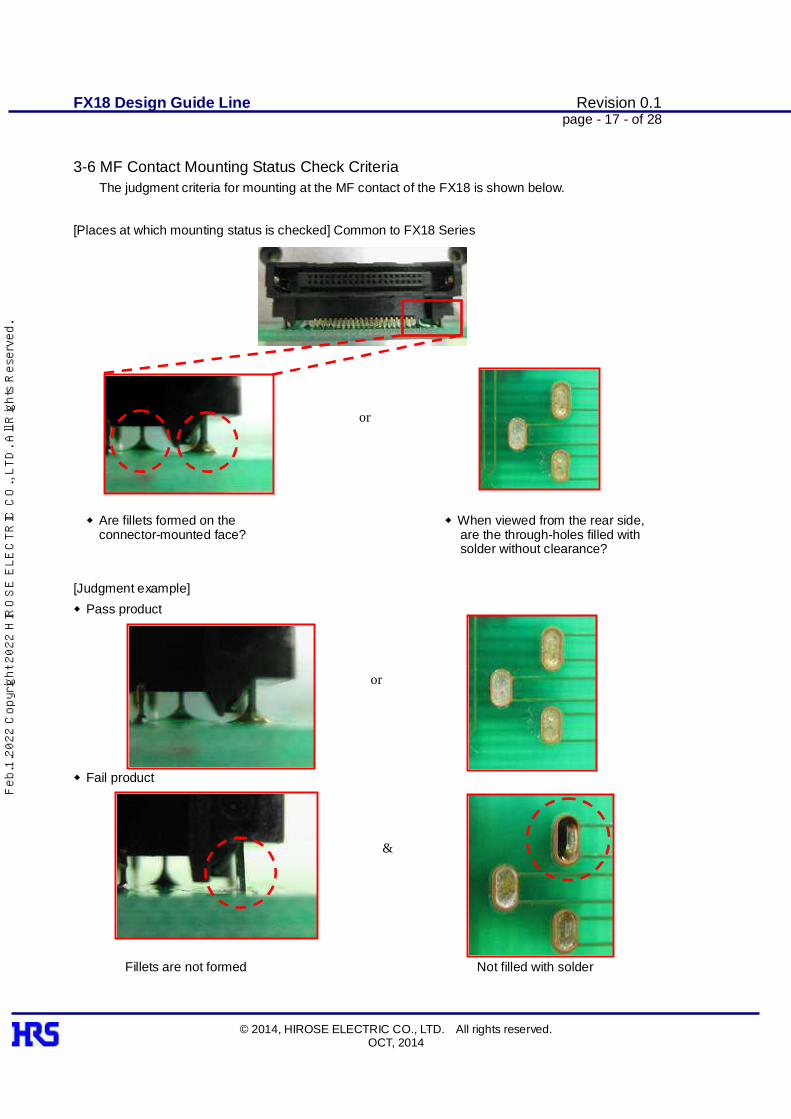
3-6 MF Contact Mounting Status Check Criteria The judgment criteria for mounting at the MF contact of the FX18 is shown below.
[Places at which mounting status is checked] Common to FX18 Series
◆Are fillets formed on the ◆When viewed from the rear side, connector-mounted face? are the through-holes filled with
solder without clearance? [Judgment example] ◆Pass product ◆Fail product
Fillets are not formed Not filled with solder
or
or
&
Feb
.1.2
022
Cop
yrig
ht 2
022
HIR
OS
E E
LEC
TR
IC C
O.,
LTD
. All
Rig
hts
Res
erve
d.

FX18 Design Guide Line Revision 0.1 page - 18 - of 28
© 2014, HIROSE ELECTRIC CO., LTD. All rights reserved. OCT, 2014
3-7 Mounting of Multiple Connectors Note that multiple connectors of the FX18 Series cannot be mounted on one board. Permitted board designs are shown in the next section.
<Not allowed> Vertical connection type Coplanar connection type Stacking connection type
■ Two or more connectors are used on one board
<Permitted> Vertical connection type Coplanar connection type Stacking connection type
■ Boards are separated
Stacking connection type ■ Boards are separated (when stacking types with different heights are used)
Feb
.1.2
022
Cop
yrig
ht 2
022
HIR
OS
E E
LEC
TR
IC C
O.,
LTD
. All
Rig
hts
Res
erve
d.

FX18 Design Guide Line Revision 0.1 page - 19 - of 28
© 2014, HIROSE ELECTRIC CO., LTD. All rights reserved. OCT, 2014
3-8 Soldering Repair Procedure If a soldering defect such as insufficient solder or solder bridge occurs when reflowing an FX18 Series connector, there are cases where it can be repaired. Its procedure is shown below as reference. [Required equipment] ・Soldering iron (a product with a bit temperature
adjustment function is recommended) ・Fixing jig of the repair target board [Required consumables] ・Solder absorbent wire (solder wick wire) ・Lead-free wire solder (φ0.2mm) [Work procedure]
(1) Fix the repair target board with a fixing jig to facilitate repair work.
For the inner contacts of the FX18-**P/S-0.8SH, the leads of the contacts are placed in a recessed position. Therefore, fixing the board with about 45 degrees tilted makes repair work easier.
(2) Perform repair work. For the detailed work method, follow the steps in the subsequent sections.
Equipment used in this document
Soldering iron FX-951 (Hakko Corporation) Shape of soldering iron bit: T12-B2
Feb
.1.2
022
Cop
yrig
ht 2
022
HIR
OS
E E
LEC
TR
IC C
O.,
LTD
. All
Rig
hts
Res
erve
d.

FX18 Design Guide Line Revision 0.1 page - 20 - of 28
© 2014, HIROSE ELECTRIC CO., LTD. All rights reserved. OCT, 2014
[When a bridge is formed <when the volume of solder is large>] If a bridge is formed between adjacent leads due to excess solder, use a commercially available solder absorbent wire (solder wick wire). [Detailed work procedure]
(1) Place a solder absorbent wire on the bridged portion.
(2) Place the soldering iron on the solder absorbent wire lightly and (3) Slide the iron bit and the absorbent wire toward you at the same time promptly
while absorbing excess solder.
(4) Repair work is completed. Caution! ○ Take care not to cause thermal deformation of the housing and deformation of leads. ○ After repair work is completed, check that sufficient soldering fillets are formed. ○ For the operating condition and iron bit shape, make an adjustment in accordance with the situation. (Reference work condition) Iron bit temperature: 350 °C, Iron bit contact time: 3 seconds
Feb
.1.2
022
Cop
yrig
ht 2
022
HIR
OS
E E
LEC
TR
IC C
O.,
LTD
. All
Rig
hts
Res
erve
d.

FX18 Design Guide Line Revision 0.1 page - 21 - of 28
© 2014, HIROSE ELECTRIC CO., LTD. All rights reserved. OCT, 2014
[When a bridge is formed <when the volume of solder is small>] If excess solder is small, there are cases where the bridge can be removed without using a solder absorbent wire. [Detailed work procedure]
(1) Place the iron bit directly on the bridged portion. (2) Slide the iron bit toward you promptly.
(3) Repair work is completed. Caution! ○ Take care not to cause thermal deformation of the housing and deformation of leads. ○ After repair work is completed, check that sufficient soldering fillets are formed. ○ For the operating condition and iron bit shape, make an adjustment in accordance with the situation. (Reference work condition) Iron bit temperature: 350 °C, Iron bit contact time: 2 seconds
Feb
.1.2
022
Cop
yrig
ht 2
022
HIR
OS
E E
LEC
TR
IC C
O.,
LTD
. All
Rig
hts
Res
erve
d.

FX18 Design Guide Line Revision 0.1 page - 22 - of 28
© 2014, HIROSE ELECTRIC CO., LTD. All rights reserved. OCT, 2014
[Insufficient solder] When there is a place where no solder is applied partially as shown in the photograph at right, use commercially available lead-free wire solder (φ 0.2mm). [Detailed work procedure]
(1) Place the iron bit directly between the lead where no solder is applied and the board pad. (The work target in the photo is the place at right where no solder is applied.)
(2) Add an appropriate amount of wire solder by pouring it.
(3) Repair work is completed. Caution! ○ Take care not to cause thermal deformation of the housing and deformation of leads. ○ After repair work is completed, check that sufficient soldering fillets are formed. ○ For the operating condition and iron bit shape, make an adjustment in accordance with the situation. (Reference work condition) Iron bit temperature: 350 °C, Iron bit contact time: 3 seconds (including the time required for pouring solder)
Feb
.1.2
022
Cop
yrig
ht 2
022
HIR
OS
E E
LEC
TR
IC C
O.,
LTD
. All
Rig
hts
Res
erve
d.

FX18 Design Guide Line Revision 0.1 page - 23 - of 28
© 2014, HIROSE ELECTRIC CO., LTD. All rights reserved. OCT, 2014
4. Requirements 4-1 Requirements on Mating (1) Requirements on self-alignment range (in the worst case) (2) Requirements on mating status (in the worst case)
Longitudinal direction self-alignment range (one side): 1.1mm
Width direction self-alignment range (one side): 0.7mm
Mating backlash in the longitudinal direction (one side): 0.015mm
Mating backlash in the width direction (one side): 0.015mm
Mating tilt in the longitudinal direction: 0.5 degrees max.
Mating tilt in the longitudinal direction: 1 degree max.
Mating clearance: 1m
m m
ax.
Feb
.1.2
022
Cop
yrig
ht 2
022
HIR
OS
E E
LEC
TR
IC C
O.,
LTD
. All
Rig
hts
Res
erve
d.
FX18 Design Guide Line Revision 0.1 page - 24 - of 28
© 2014, HIROSE ELECTRIC CO., LTD. All rights reserved. OCT, 2014
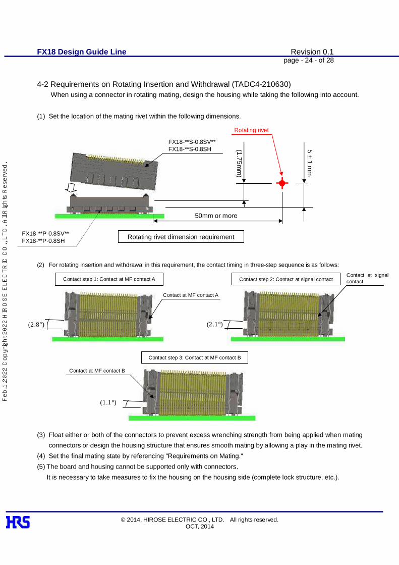
4-2 Requirements on Rotating Insertion and Withdrawal (TADC4-210630) When using a connector in rotating mating, design the housing while taking the following into account.
(1) Set the location of the mating rivet within the following dimensions. (2) For rotating insertion and withdrawal in this requirement, the contact timing in three-step sequence is as follows:
(3) Float either or both of the connectors to prevent excess wrenching strength from being applied when mating
connectors or design the housing structure that ensures smooth mating by allowing a play in the mating rivet. (4) Set the final mating state by referencing "Requirements on Mating." (5) The board and housing cannot be supported only with connectors. It is necessary to take measures to fix the housing on the housing side (complete lock structure, etc.).
50mm or more
5 ± 1 mm
Rotating rivet
(1.75mm
)
FX18-**P-0.8SV** FX18-**P-0.8SH
FX18-**S-0.8SV** FX18-**S-0.8SH
Rotating rivet dimension requirement
(2.8°)
Contact step 1: Contact at MF contact A Contact step 2: Contact at signal contact
Contact at MF contact A
(2.1°)
Contact at signal contact
Contact step 3: Contact at MF contact B
Contact at MF contact B
(1.1°) Feb
.1.2
022
Cop
yrig
ht 2
022
HIR
OS
E E
LEC
TR
IC C
O.,
LTD
. All
Rig
hts
Res
erve
d.

FX18 Design Guide Line Revision 0.1 page - 25 - of 28
© 2014, HIROSE ELECTRIC CO., LTD. All rights reserved. OCT, 2014
4-3 Recommended Spacer Dimensions (Stacking Connection Type) Be sure to use a spacer between boards using the FX18 Series stacking type connectors so that load is not applied to the solder joint parts and connectors.
[When two pieces are used] [When three pieces are used]
When two pieces are used When three pieces are used
Stacking height
Plug/receptacle product name Recommended spacer
height dimensions
10 mm FX18-**P-0.8SV/FX18-**S-0.8SV10 10.3 ± 0.127 mm
15 mm FX18-**P-0.8SV/FX18-**S-0.8SV15 15 ± 0.127 mm
20 mm FX18-**P-0.8SV/FX18-**S-0.8SV20 20 ± 0.127 mm
20 mm FX18-**P-0.8SV10/FX18-**S-0.8SV10 20.3 ± 0.127 mm
25 mm FX18-**P-0.8SV10/FX18-**S-0.8SV15 25 ± 0.127 mm 30 mm FX18-**P-0.8SV10/FX18-**S-0.8SV20 30 ± 0.127 mm
Stacking height
plug Interposer Receptacle Recommended spacer
height dimensions
25 mm FX18-**P-0.8SV FX18-**PS-0.8H15 FX18-**S-0.8SV10 25.3 ± 0.127 mm
30 mm FX18-**P-0.8SV FX18-**PS-0.8H15 FX18-**S-0.8SV15 30 ± 0.127 mm
35 mm FX18-**P-0.8SV FX18-**PS-0.8H15 FX18-**S-0.8SV20 35 ± 0.127 mm
35 mm FX18-**P-0.8SV10 FX18-**PS-0.8H15 FX18-**S-0.8SV10 35.3 ± 0.127 mm
40 mm FX18-**P-0.8SV10 FX18-**PS-0.8H15 FX18-**S-0.8SV15 40 ± 0.127 mm
45mm FX18-**P-0.8SV10 FX18-**PS-0.8H15 FX18-**S-0.8SV20 45 ± 0.127 mm
Spacer
Plug
Receptacle
Plug
Receptacle
Interposer
Feb
.1.2
022
Cop
yrig
ht 2
022
HIR
OS
E E
LEC
TR
IC C
O.,
LTD
. All
Rig
hts
Res
erve
d.

FX18 Design Guide Line Revision 0.1 page - 26 - of 28
© 2014, HIROSE ELECTRIC CO., LTD. All rights reserved. OCT, 2014
5. Caution 5-1 Use of Interposers
An interposer is equipped with a simple locking device to improve the mating strength. It is designed to be always left on the receptacle side when the header is removed away.
Simple locking device
Before using the interposer, read the following caution.
(1) Because the mating fixed side is equipped with a simple lock, it is not removed easily. The number of times of insertion and withdrawal should not exceed five times.
(2) When mating connectors, be sure to mate the mating fixed side first, and then mate the insertion and
withdrawal side. (3) Only for the insertion and withdrawal side, the effective mating length of each contact is 2.5mm for an
MF contact A, 2mm for a signal contact, and 1.5mm for an MF contact B. (4) For the allowable clearance between the mated pair, zero on the mating fixed side and 1mm or less only
on the insertion and withdrawal side.
[Insertion and withdrawal side]
Header: Male contact
Interposer: Female contact
[Fixed side]
Interposer: Male contact
Receptacle: Female contact
Interposer is P/S type
Feb
.1.2
022
Cop
yrig
ht 2
022
HIR
OS
E E
LEC
TR
IC C
O.,
LTD
. All
Rig
hts
Res
erve
d.

FX18 Design Guide Line Revision 0.1 page - 27 - of 28
© 2014, HIROSE ELECTRIC CO., LTD. All rights reserved. OCT, 2014
5-2 Allowable Clearance between the Mated Pair The effective mating length of each contact is 2.5mm for an MF contact A, 2mm for a signal contact, and 1.5mm for an MF contact B. (*1) Make certain that the clearance between the header and the receptacle at the time of mating does not exceed 1mm.
[Coplanar connection type] [Vertical connection type] [Stacking connection type (two pieces)] [Stacking connection type (three pieces)]
(* 1) Because the effective mating length is set to 1.5mm for an MF contact A, 1mm for a signal contact, and 1mm for an MF contact B only on the interposer fixed side, there is no allowable clearance between the mated pair on the mating fixed side.
1mm or less 1mm or less
1mm or less 1mm or less
[Inse
rtion
and
with
draw
al s
ide]
[F
ixed
sid
e]
Feb
.1.2
022
Cop
yrig
ht 2
022
HIR
OS
E E
LEC
TR
IC C
O.,
LTD
. All
Rig
hts
Res
erve
d.

FX18 Design Guide Line Revision 0.1 page - 28 - of 28
© 2014, HIROSE ELECTRIC CO., LTD. All rights reserved. OCT, 2014
FFXX1188 SSeerriieess DDeessiiggnn GGuuiiddee LLiinnee Revision history
Revision Date Handled by Comments 0.1 Oct 7, 2014 PCC Asao First edition
Version number 0.1 Prepared by PCC Asao Reviewed by PCC Yamaguchi Approved by PCC Okawa
Feb
.1.2
022
Cop
yrig
ht 2
022
HIR
OS
E E
LEC
TR
IC C
O.,
LTD
. All
Rig
hts
Res
erve
d.