high performance position servo control ic
TRANSCRIPT
IRMCF143
1 www.irf.com © 2015 International Rectifier February 4,2015
High Performance Position Servo Control IC
Description IRMCF143 is a high performance Flash based motion control IC designed primarily for position servo applications based on an incremental encoder. IRMCF143 is designed to achieve low cost yet high performance control solutions for advanced inverterized servo motor control. IRMCF143 contains two computation engines. One is the Flexible Motion Control Engine (MCE
TM) for sinusoidal Field Oriented Control (FOC) of servo motors; the other is
an 8-bit high-speed microcontroller (8051). Both computation engines are integrated into one monolithic chip. The MCE
TM contains a collection of control elements implemented in a dedicated computation engine such as
Proportional plus Integral, Vector rotator, Angle estimator, Multiply/Divide, and Low loss SVPWM. The user can program a motion control algorithm by connecting these control elements using a graphic compiler. A unique analog/digital circuit and algorithm to fully support two leg shunt current sensing is also provided. The 8051 microcontroller performs 2-cycle instruction execution (15MIPS at 30MHz 8051CLK). The MCE and 8051 microcontroller are connected via dual port RAM for signal monitoring and command input. An advanced graphic compiler for the MCE
TM is seamlessly integrated into the MATLAB/Simulink environment, while third party JTAG-
based emulator tools are supported for 8051 software development. IRMCF143 comes in a 64 pin QFP package.
Features MCE
TM (Flexible Motion Control Engine) -
Dedicated computation engine for high efficiency sinusoidal FOC control
Built-in hardware peripheral for two shunt current feedback reconstruction and analog circuits
Supports incremental encoder with Hall effect position sensor initialization
24bit position counter
Position capture and compare
Pulse + Direction input
Brake control with gatekill input
Loss minimization Space Vector PWM
Three-channel analog outputs (PWM)
Embedded 8-bit high speed microcontroller (8051) for flexible I/O and man-machine control
JTAG programming port for emulation/debugger
Serial communication interface (UART)
I2C/SPI serial interface
Three general purpose timers, one capture timer
Watchdog timer with independent internal clock
Internal 64 Kbyte flash memory
3.3V single supply
Product Summary Maximum clock input (fcrystal) 60MHz
Maximum Internal clock (SYSCLK) 120MHz
Maximum 8051 clock (8051CLK) 30MHz
FOC computation time 35 μsec@100MHz
MCETM
computation data range 16 bit signed
8051 Program Flash 52KB
8051/MCE Data RAM 4KB
MCE Program RAM 12KB
GateKill latency (digital filtered) 2 μsec
PWM carrier frequency 20 bits/ SYSCLK
A/D input channels 8
A/D converter resolution 12 bits
A/D converter conversion speed 2 μsec
Analog output (PWM) resolution 8 bits
UART baud rate (typ) 57.6K bps
Encoder interface 6
Number of digital I/O (max) 22
Package (lead free) QFP64
Ordering Information
Orderable Part Number Package Type Standard Pack
Form Quantity
IRMCF143TR LQFP64 Tape and Reel 1500
IRMCF143TY LQFP64 Tray 1600

IRMCF143
2 www.irf.com © 2015 International Rectifier February 4,2015
Table of Contents
1 Overview ................................................................................................................................. 5 2 Pinout ..................................................................................................................................... 6 3 IRMCF143 Block Diagram and Main Functions ............................................................................. 7 4 Application connection and Pin function ..................................................................................... 8
4.1 8051 Peripheral Interface Group ................................................................................................................. 9 4.2 Motion Peripheral Interface Group ............................................................................................................. 10 4.3 Analog Interface Group .............................................................................................................................. 10 4.4 Power Interface Group ............................................................................................................................... 11 4.5 Test Interface Group .................................................................................................................................. 11
5 DC Characteristics ................................................................................................................. 11 5.1 Absolute Maximum Ratings ....................................................................................................................... 12 5.2 System Clock Frequency and Power Consumption .................................................................................. 12 5.3 Digital I/O DC Characteristics .................................................................................................................... 13 5.4 PLL and Oscillator DC characteristics ....................................................................................................... 14 5.5 Analog I/O DC Characteristics ................................................................................................................... 14 5.6 Under Voltage Lockout DC characteristics ................................................................................................ 15 5.7 Itrip comparator DC characteristics............................................................................................................ 15 5.8 CMEXT and AREF Characteristics ............................................................................................................ 15
6 AC Characteristics ................................................................................................................. 16 6.1 Digital PLL AC Characteristics ................................................................................................................... 16 6.2 Analog to Digital Converter AC Characteristics ......................................................................................... 17 6.3 Op amp AC Characteristics ....................................................................................................................... 18 6.4 SYNC to SVPWM and A/D Conversion AC Timing ................................................................................... 19 6.5 GATEKILL to SVPWM AC Timing ............................................................................................................. 20 6.6 Itrip AC Timing ........................................................................................................................................... 20 6.7 Interrupt AC Timing .................................................................................................................................... 21 6.8 I
2C AC Timing ............................................................................................................................................ 22
6.9 SPI AC Timing............................................................................................................................................ 23 SPI Write AC timing ................................................................................................................................... 23 SPI Read AC Timing .................................................................................................................................. 24
6.10 UART AC Timing ....................................................................................................................................... 25 6.11 CAPTURE Input AC Timing ....................................................................................................................... 26 6.12 JTAG AC Timing ........................................................................................................................................ 27
7 I/O Structure .......................................................................................................................... 28 8 Pin List ................................................................................................................................. 31 9 Package Dimensions .............................................................................................................. 33 10 Part Marking Information ......................................................................................................... 34 11 Qualification Information ......................................................................................................... 34
IRMCF143
3 www.irf.com © 2015 International Rectifier February 4,2015
List of Tables
Table 1. Absolute Maximum Ratings ................................................................................................................... 12
Table 2. System Clock Frequency ....................................................................................................................... 12
Table 3. Digital I/O DC Characteristics ................................................................................................................ 13
Table 4. PLL DC Characteristics ......................................................................................................................... 14
Table 5. Analog I/O DC Characteristics ............................................................................................................... 14
Table 6. UVcc DC Characteristics ....................................................................................................................... 15
Table 7. Itrip DC Characteristics .......................................................................................................................... 15
Table 8. CMEXT and AREF DC Characteristics ................................................................................................. 15
Table 9. PLL AC Characteristics .......................................................................................................................... 16
Table 10. A/D Converter AC Characteristics ......................................................................................................... 17
Table 11. Current Sensing OP Amp AC Characteristics ....................................................................................... 18
Table 12. SYNC AC Characteristics ...................................................................................................................... 19
Table 13. GATEKILL to SVPWM AC Timing ......................................................................................................... 20
Table 14. Itrip AC Timing ....................................................................................................................................... 20
Table 15. Interrupt AC Timing ................................................................................................................................ 21
Table 16. I2C AC Timing ........................................................................................................................................ 22
Table 17. SPI Write AC Timing .............................................................................................................................. 23
Table 18. SPI Read AC Timing .............................................................................................................................. 24
Table 19. UART AC Timing ................................................................................................................................... 25
Table 20. CAPTURE AC Timing ............................................................................................................................ 26
Table 21. JTAG AC Timing .................................................................................................................................... 27
Table 22. Pin List ................................................................................................................................................... 32
IRMCF143
4 www.irf.com © 2015 International Rectifier February 4,2015
List of Figures
Figure 1. Typical Application Block Diagram Using IRMCF143 .................................................................................5
Figure 2. Pinout of IRMCF143 ....................................................................................................................................6
Figure 3. IRMCF143 Block Diagram ...........................................................................................................................7
Figure 4. IRMCF143 Application Diagram ..................................................................................................................8
Figure 5. Crystal circuit example ............................................................................................................................. 16
Figure 6. Voltage droop and S/H hold time ............................................................................................................. 17
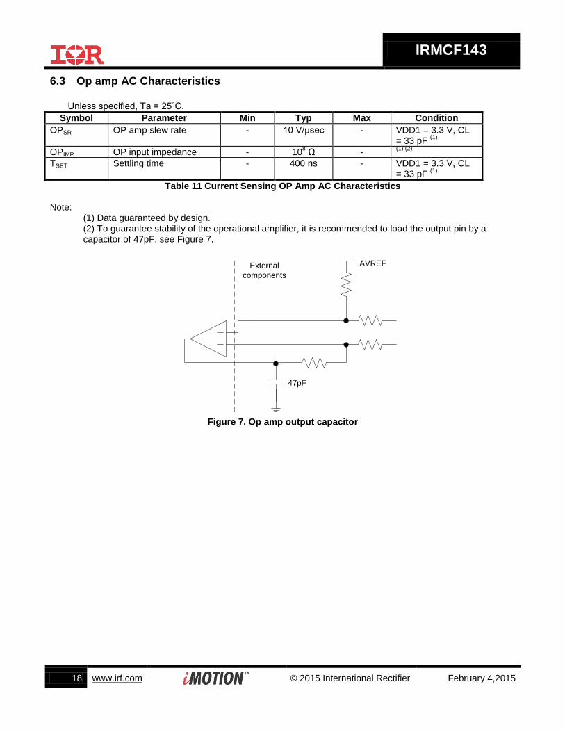
Figure 7. Op amp output capacitor .......................................................................................................................... 18
Figure 8. SYNC timing ............................................................................................................................................. 19
Figure 9. Gatekill timing ........................................................................................................................................... 20
Figure 10. ITRIP timing ............................................................................................................................................ 20
Figure 11. Interrupt timing ....................................................................................................................................... 21
Figure 12. I2C Timing ............................................................................................................................................... 22
Figure 13. SPI write timing ...................................................................................................................................... 23
Figure 14. SPI read timing ....................................................................................................................................... 24
Figure 15. UART timing ........................................................................................................................................... 25
Figure 16. CAPTURE timing .................................................................................................................................... 26
Figure 17. JTAG timing ............................................................................................................................................ 27
Figure 18. PWMUL/PWMUH/PWMVL/PWMVH/PWMWL/PWMWH/BRAKE output .............................................. 28
Figure 19. All digital I/O except PWM output ........................................................................................................... 28
Figure 20. RESET, GATEKILL I/O .......................................................................................................................... 28
Figure 21. Analog input ........................................................................................................................................... 29
Figure 22. Analog operational amplifier output and AREF I/O structure ................................................................. 29
Figure 23. VSS,AVSS pin I/O structure ................................................................................................................... 29
Figure 24. VDD1,VDDCAP pin I/O structure ........................................................................................................... 30
Figure 25. XTAL0/XTAL1 pins structure .................................................................................................................. 30
IRMCF143
5 www.irf.com © 2015 International Rectifier February 4,2015
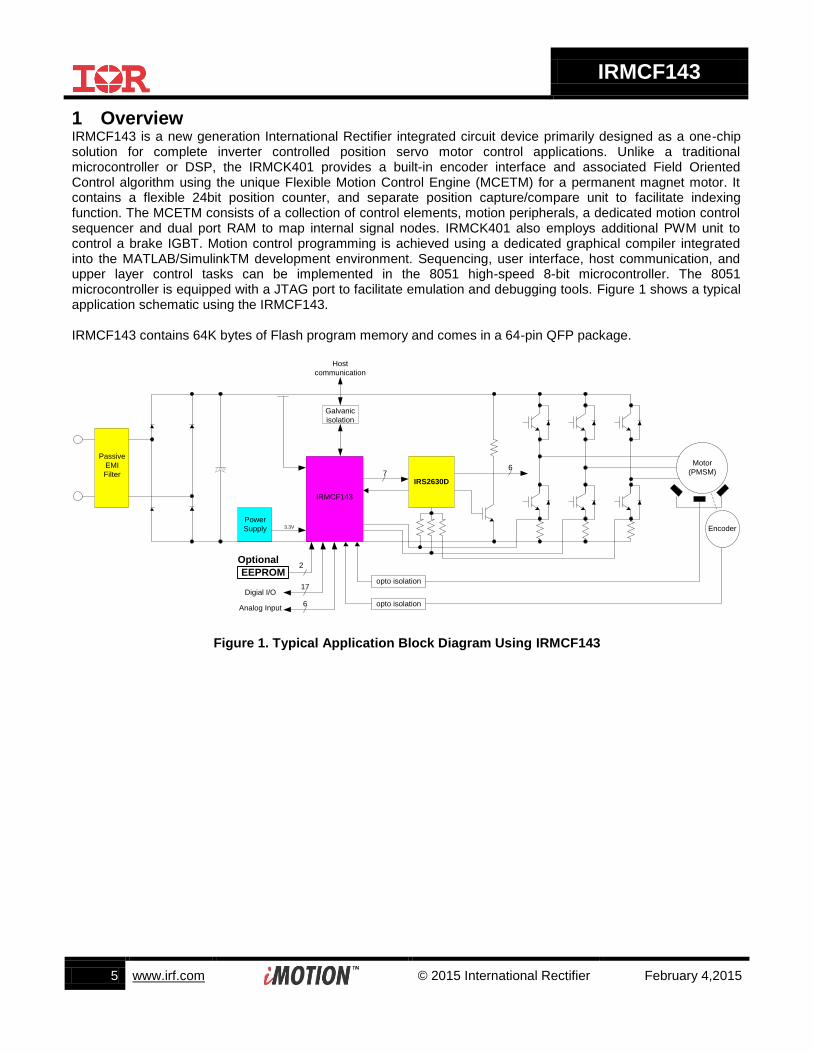
1 Overview IRMCF143 is a new generation International Rectifier integrated circuit device primarily designed as a one-chip solution for complete inverter controlled position servo motor control applications. Unlike a traditional microcontroller or DSP, the IRMCK401 provides a built-in encoder interface and associated Field Oriented Control algorithm using the unique Flexible Motion Control Engine (MCETM) for a permanent magnet motor. It contains a flexible 24bit position counter, and separate position capture/compare unit to facilitate indexing function. The MCETM consists of a collection of control elements, motion peripherals, a dedicated motion control sequencer and dual port RAM to map internal signal nodes. IRMCK401 also employs additional PWM unit to control a brake IGBT. Motion control programming is achieved using a dedicated graphical compiler integrated into the MATLAB/SimulinkTM development environment. Sequencing, user interface, host communication, and upper layer control tasks can be implemented in the 8051 high-speed 8-bit microcontroller. The 8051 microcontroller is equipped with a JTAG port to facilitate emulation and debugging tools. Figure 1 shows a typical application schematic using the IRMCF143. IRMCF143 contains 64K bytes of Flash program memory and comes in a 64-pin QFP package.
IRMCF143
Power
Supply
IRS2630D
Digial I/O
3.3V
Passive
EMI
Filter
Host
communication
Motor
(PMSM)
Galvanic
isolation
EEPROM
Analog Input
17
6
2Optional
Encoder
opto isolation
opto isolation
76
Figure 1. Typical Application Block Diagram Using IRMCF143
IRMCF143
6 www.irf.com © 2015 International Rectifier February 4,2015
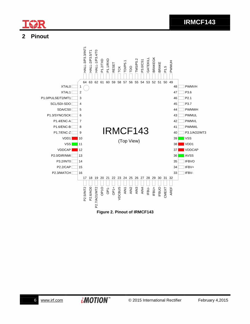
2 Pinout
17 18 19 20 21 22 23 24 25 26 27 28 29 30 31 32
15
14
13
16
3
12
4
11
5
6
7
8
9
10
2
1
SCL/SDI-SDO
SDA/CS0
VDD1
VSS
VDDCAP
P1.3/SYNC/SCK
P1.4/ENC-A
P3.2/INT0
34
35
36
33
46
37
45
38
44
43
42
41
40
39
47
48
64 63 62 61 60 59 58 57 56 55 54 53 52 51 50 49
AIN
2
OP
1O
VD
CB
US
P2
.7/A
O1
/MT
2
P2
.6/A
O0
P2.1
P3.7
PWMWH
PWMUL
PWMVL
PWMWL
PW
MU
H
VSS
P3.1/AO2/MT3
IFB
UO
IFB
U-
IFB
U+
XTAL0
HA
LL-2
/P3.5
/T1
RE
SE
T
P1.5
TC
K
TD
I/P
5.1
TD
O
TM
S/P
5.2
P1.2
/TX
D
P1.1
/RX
D
PWMVH
P3.6
GA
TE
KIL
L
IRMCF143(Top View)
AIN
4
AIN
3
IFBVO
IFBV+
IFBV-
P2.0/DIR/NMI
P2.2/CAP
AIN
1
HA
LL-3
/P3.3
/IN
T1
P1.7/ENC-Z
P1.6/ENC-B
P1.0/PULSE/T2/MT1
P2
.5/IN
T2
BR
AK
E
BR
AK
EG
K
XTAL1
P2.3/MATCH
OP
1-
OP
1+
VDD1P
3.0
/CS
1
HA
LL-1
/P3.4
/T0
VDDCAP
AVSS
AR
EF
CM
EX
T
Figure 2. Pinout of IRMCF143
IRMCF143
7 www.irf.com © 2015 International Rectifier February 4,2015
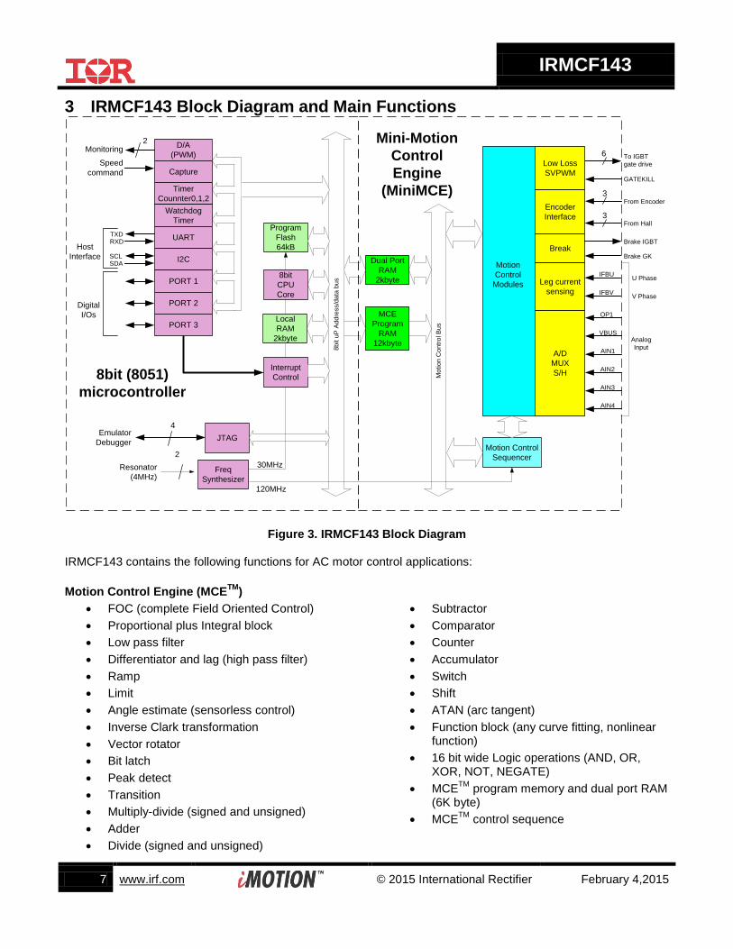
3 IRMCF143 Block Diagram and Main Functions
Motion Control
Sequencer
Dual Port
RAM
2kbyte
MCE
Program
RAM
12kbyte
Program
Flash
64kB
8b
it u
P A
dd
ress/d
ata
bu
s
Mo
tio
n C
on
tro
l B
us
A/D
MUX
S/H
D/A
(PWM)
Timer
Counnter0,1,2
Watchdog
Timer
Motion
Control
Modules
UART
I2C
TXDRXD
6
Low Loss
SVPWM
VBUS
GATEKILL
To IGBT
gate drive
Mini-Motion
Control
Engine
(MiniMCE)
Monitoring
Host
Interface
Digital
I/Os
8bit (8051)
microcontroller
AIN1
AIN2
JTAGEmulator
Debugger
4
Freq
Synthesizer
2
Resonator
(4MHz)
30MHz
AIN3
Analog
Input
2
Capture
Interrupt
Control
Encoder
Interface
From Encoder
Speed
command
PORT 1
SCLSDA
PORT 2
PORT 3
AIN4
Break
Leg current
sensing
Brake IGBT
U Phase8bit
CPU
Core
Local
RAM
2kbyte
120MHz
3
From Hall3
OP1
IFBU
IFBVV Phase
Brake GK
Figure 3. IRMCF143 Block Diagram IRMCF143 contains the following functions for AC motor control applications:
Motion Control Engine (MCETM
)
FOC (complete Field Oriented Control)
Proportional plus Integral block
Low pass filter
Differentiator and lag (high pass filter)
Ramp
Limit
Angle estimate (sensorless control)
Inverse Clark transformation
Vector rotator
Bit latch
Peak detect
Transition
Multiply-divide (signed and unsigned)
Adder
Divide (signed and unsigned)
Subtractor
Comparator
Counter
Accumulator
Switch
Shift
ATAN (arc tangent)
Function block (any curve fitting, nonlinear function)
16 bit wide Logic operations (AND, OR, XOR, NOT, NEGATE)
MCETM
program memory and dual port RAM (6K byte)
MCETM
control sequence
IRMCF143
8 www.irf.com © 2015 International Rectifier February 4,2015
8051 microcontroller
Two 16 bit timer/counters
One 16 bit periodic timer
One 16 bit watchdog timer
One 16 bit capture timer
Up to 24 discrete digital I/Os
8-channel 12 bit A/D (0 – 1.2V input)
o Three buffered channels, two use for current sensing
o Five unbuffered channels
JTAG port (4 pins)
Up to three channels of analog output (8 bit PWM)
UART
I2C/SPI port
64K byte Flash memory
2K byte data RAM
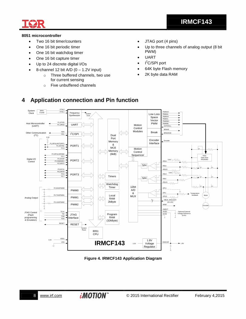
4 Application connection and Pin function
P1.2/TXD
P1.1/RXD
P1.3/SYNC
XTAL0
PWMUH
PWMUL
PWMVH
PWMVL
PWMWH
PWMWL
GATEKILL
VBUS, AIN1/2/3/4
Host Microcontroller
(UART)
Digital I/O
Control
System
Clock
4MHz
Crystal
P2.6/AOPWM0
Analog Output
XTAL1
P1.5
P3.0/CS1
RESET
TDIJTAG Control
(Flash
programming
& Emulation)
TCLK
TSM
TDO
0.6VIFBU+
IFBU-
IFBUO
(0-1.2V)
AVDD
1.8V
AVSS
VDD13.3V
VSS
CMEXT
BRAKE
IFBV+
IFBV-
IFBVO
OP1+
OP1-
OP1O
Optional External
Voltage Reference
(0.6V)
P2.7/AOPWM1
SCL
SDAOther Communication
(I2C)
Frequency
Synthesizer
UART
I2C/SPI
PORT1
PORT2
RESET
PWM0
PWM1
JTAG
Interface
Low Loss
Space
Vector
PWM
Break
S/H
S/H
8051
CPU
Dual
Port
Memory
&
MCE
Memory
(6kB)
Motion
Control
Modules
Motion
Control
Sequencer
12bit
A/D
&
MUX
System
clock
Local
RAM
2kByte
Program
RAM
(32kByte)
System
Reset
Watchdog
Timer
Timers
IRMCF143
AREFPWM2P3.1/AOPWM2
PORT3
P1.0/PULIN//T2/MT1
P2.2/CAP
P2.0/PULDIR/NMI
P2.3/QINDEX
P2.5/INT2
P3.2/INT0
5
3.3V
Encoder
1.8V
Voltage
Regulator
VDDCAP3.3V
Encoder
Temperature
feedback
P3.6
P3.7
P2.1
Motor
HVIC
Gate Drive
IRS2630D
0.6V
Encoder
Interface
BRAKEGK
Figure 4. IRMCF143 Application Diagram
IRMCF143
9 www.irf.com © 2015 International Rectifier February 4,2015
4.1 8051 Peripheral Interface Group
UART Interface P1.2/TXD Output, Transmit data from IRMCF143 P1.1/RXD Input, Receive data to IRMCF143
Discrete I/O Interface
P1.0/PULSE/T2/MT1 Input/output port 1.0, can be configured as Timer/Counter 2 input or MCE pin timer 1 output, allocated by MCE as Pulse Input
P1.1/RXD Input/output port 1.1, can be configured as RXD input P1.2/TXD Input/output port 1.2, can be configured as TXD output P1.3/SYNC/SCK Input/output port 1.3, can be configured as SYNC output or SPI clock output P1.4/ENC-A Input/output port 1.4, allocated by MCE as Encoder-A input P1.5 Input/output port 1.5 P1.6/ENC-B Input/output port 1.6, allocated by MCE as Encoder-B input P1.7/ENC-Z Input/output port 1.7, allocated by MCE as Encoder-Z input P2.0/DIR/NMI Input/output port 2.0, can be configured as non-maskable interrupt input, allocated
by MCE as Direction Input P2.1 Input/output port 2.1 P2.2/CAP Input/output port 2.2, can be configured as capture timer input P2.3/MATCH Input/output port 2.3, can be configured as MATCH output P2.5/INT2 Input/output port 2.5, can be configured as INT2 input P2.6/AO0 Input/output port 2.6, can be configured as AO0 output P2.7/AO1/MT2 Input/output port 2.7, can be configured as AO1 output or MCE pin timer 2 output P3.0/CS1 Input/output port 3.0, can be configured as SPI chip select 1 P3.1/AO2/MT3 Input/output port 3.1, can be configured as AO2 output or MCE pin timer 3 output P3.2/INT0 Input/output port 3.2, can be configured as INT0 input P3.3/HALL-3/INT1 Input/output port 3.3, can be configured as INT1 input, allocated by MCE as Hall-3
input P3.4/HALL-1/T0 Input/output port 3.4, can be configured as Timer 0 input, allocated by MCE as Hall-
1 input P3.5/HALL-2/T1 Input/output port 3.5, can be configured as Timer 1 input, allocated by MCE as Hall-
2 input P3.6 Input/output port 3.6 P3.7 Input/output port 3.7 P5.1/TDI Input port 5.1, configured as JTAG port by default P5.2/TMS Input port 5.2, configured as JTAG port by default
Analog Output Interface P2.6/AO0 Input/output, can be configured as 8-bit PWM output 0 with programmable carrier
frequency P2.7/AO1 Input/output, can be configured as 8-bit PWM output 1 with programmable carrier
frequency P3.1/AO2 Input/output, can be configured as 8-bit PWM output 2 with programmable carrier
frequency Crystal Interface
XTAL0 Input, connected to crystal XTAL1 Output, connected to crystal
Reset Interface
RESET Input and Output, system reset, doesn’t require external RC time constant I2C Interface
SCL/SO-SI Output, I2C clock output, or SPI data
SDA/CS0 Input/output, I2C Data line or SPI chip select 0

IRMCF143
10 www.irf.com © 2015 International Rectifier February 4,2015
I2C/SPI Interface
SCL/SO-SI Output, I2C clock output, or SPI data
SDA/CS0 Input/output, I2C data line or SPI chip select 0
P1.3/SYNC/SCK Input/output port 1.3, can be configured as SYNC output or SPI clock output P3.0/CS1 Input/output port 3.0, can be configured as SPI chip select 1
4.2 Motion Peripheral Interface Group
PWM PWMUH Output, PWM phase U high side gate signal, internally pulled down by 58kΩ,
configured high true at a power up PWMUL Output, PWM phase U low side gate signal, internally pulled down by 58kΩ,
configured high true at a power up PWMVH Output, PWM phase V high side gate signal, internally pulled down by 58kΩ,
configured high true at a power up PWMVL Output, PWM phase V low side gate signal, internally pulled down by 58kΩ,
configured high true at a power up PWMWH Output, PWM phase W high side gate signal, internally pulled down by 58kΩ,
configured high true at a power up PWMWL Output, PWM phase W low side gate signal, internally pulled down by 58kΩ,
configured high true at a power up BRAKE Output, BRAKE output signal, internally pulled up by 70kΩ, configured low true at a
power up Fault
GATEKILL Input, upon assertion this negates all six PWM signals, active low, internally pulled up by 70kΩ
BRAKEGK Input, upon assertion, this negates BRAKE signal, active low, internally pulled up by 70kΩ
4.3 Analog Interface Group
AVSS Analog power return, (analog internal 1.8V power is shared with VDDCAP) AREF 0.6V buffered output CMEXT Unbuffered 0.6V, input to the AREF buffer, capacitor needs to be connected. OP1+ Input, Operational amplifier positive input for application sensing OP1- Input, Operational amplifier negative input for application sensing OP1O Output, Operational amplifier output for application sensing IFBU+ Input, Operational amplifier positive input for U phase current sensing IFBU- Input, Operational amplifier negative input for U phase current sensing IFBUO Output, Operational amplifier output for U phase current sensing IFBV+ Input, Operational amplifier positive input for V phase current sensing IFBV- Input, Operational amplifier negative input for V phase current sensing IFBVO Output, Operational amplifier output for V phase current sensing VDCBUS Input, Analog input channel (0 – 1.2V), allocated for DC bus voltage input AIN1 Input, Analog input channel 1 (0 – 1.2V), allocated by MCE as speed input, needs to
be pulled down to AVSS if unused AIN2 Input, Analog input channel 2 (0 – 1.2V), allocated by MCE as torque input, needs to
be pulled down to AVSS if unused

IRMCF143
11 www.irf.com © 2015 International Rectifier February 4,2015
AIN3 Input, Analog input channel 3 (0 – 1.2V), needs to be pulled down to AVSS if unused
AIN4 Input, Analog input channel 4 (0 – 1.2V), needs to be pulled down to AVSS if unused
4.4 Power Interface Group
VDD1 Digital power (3.3V) VDDCAP Internal 1.8V output, requires capacitors to the pin. Shared with analog power pad
internally Note: The internal 1.8V supply is not designed to power any external circuits or
devices. Only capacitors should be connected to this pin. VSS Digital common
4.5 Test Interface Group
P5.2/TMS JTAG test mode input or input digital port TDO JTAG data output P5.1/TDI JTAG data input, or input digital port TCK JTAG test clock
4.6 Incremental Encoder/Hall sensor Group
P1.4/ENC-A Incremental Encoder A input P1.6/ENC-B Incremental Encoder B input P1.7/ENC-Z Incremental Encoder Z input P3.3/HALL-3/INT1 Hall sensor 3 input P3.4/HALL-1/T0 Hall sensor 1 input P3.5/HALL-2/T1 Hall sensor 2 input

IRMCF143
12 www.irf.com © 2015 International Rectifier February 4,2015
5 DC Characteristics
5.1 Absolute Maximum Ratings
Symbol Parameter Min Typ Max Condition
VDD1 Supply Voltage -0.3 V - 3.6 V Respect to VSS
VIA Analog Input Voltage -0.3 V - 1.98 V Respect to AVSS
VID Digital Input Voltage -0.3 V - 6.0 V Respect to VSS
TA Ambient Temperature -40 ˚C - 85 ˚C
TS Storage Temperature -65 ˚C - 150 ˚C
Table 1. Absolute Maximum Ratings Caution: Stresses beyond those listed in “Absolute Maximum Ratings” may cause permanent damage to the device. These are stress ratings only and function of the device at these or any other conditions beyond those indicated in the operational sections of the specifications are not implied.
5.2 System Clock Frequency and Power Consumption
CAREF = 1nF, CMEXT= 100nF. VDD1=3.3V, Unless specified, Ta = 25˚C.
Symbol Parameter Min Typ Max Unit
SYSCLK System Clock 32 - 120 MHz
PD Power consumption 1001)
- mW
Table 2. System Clock Frequency
Note 1) The value is based on the condition of MCE clock=100MHz, 8051 clock 20MHz with a actual motor running by a typical MCE application program and 8051 code.
IRMCF143
13 www.irf.com © 2015 International Rectifier February 4,2015
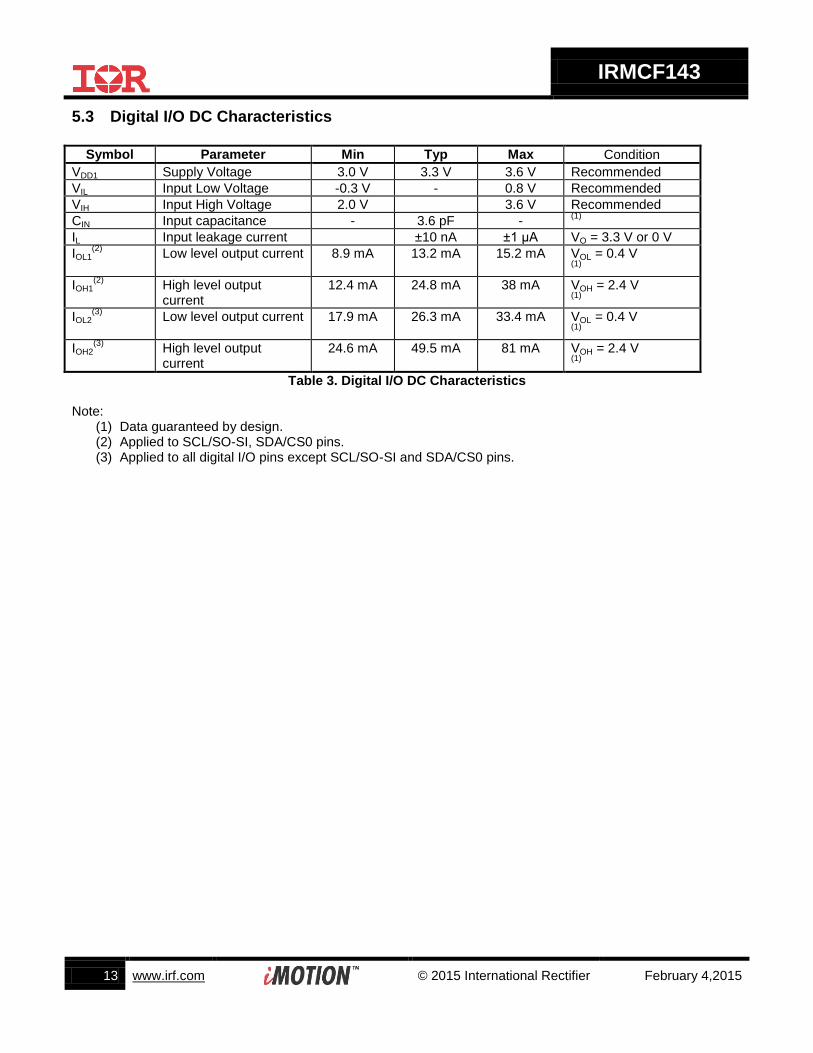
5.3 Digital I/O DC Characteristics
Symbol Parameter Min Typ Max Condition
VDD1 Supply Voltage 3.0 V 3.3 V 3.6 V Recommended
VIL Input Low Voltage -0.3 V - 0.8 V Recommended
VIH Input High Voltage 2.0 V 3.6 V Recommended
CIN Input capacitance - 3.6 pF - (1)
IL Input leakage current ±10 nA ±1 μA VO = 3.3 V or 0 V
IOL1(2)
Low level output current 8.9 mA 13.2 mA 15.2 mA VOL = 0.4 V (1)
IOH1(2)
High level output current
12.4 mA 24.8 mA 38 mA VOH = 2.4 V (1)
IOL2(3)
Low level output current 17.9 mA 26.3 mA 33.4 mA VOL = 0.4 V (1)
IOH2(3)
High level output current
24.6 mA 49.5 mA 81 mA VOH = 2.4 V (1)
Table 3. Digital I/O DC Characteristics Note:
(1) Data guaranteed by design. (2) Applied to SCL/SO-SI, SDA/CS0 pins. (3) Applied to all digital I/O pins except SCL/SO-SI and SDA/CS0 pins.

IRMCF143
14 www.irf.com © 2015 International Rectifier February 4,2015
5.4 PLL and Oscillator DC characteristics
CAREF = 1nF, CMEXT= 100nF. VDD1=3.3V, Unless specified, Ta = 25˚C.
Symbol Parameter Min Typ Max Condition
VIL OSC Oscillator (XTAL0,1) Input Low Voltage
0 - 0.2* VDDCAP VDDCAP = voltage at VDDCAP pin
VIH OSC Oscillator (XTAL0,1) Input High Voltage
0.8* VDDCAP - VDDCAP VDDCAP = voltage at VDDCAP pin
Table 4 PLL DC Characteristics
5.5 Analog I/O DC Characteristics
- OP amps for application sensing (OP1+, OP1-, OP1O, OP2+, OP2-, OP2O, OP3+, OP3-, OP3O) CAREF = 1nF, CMEXT= 100nF. VDD1=3.3V, Unless specified, Ta = 25˚C.
Symbol Parameter Min Typ Max Condition
VOFFSET Input Offset Voltage - - 26 mV VAVDD = 1.8 V
VI Input Voltage Range 0 V 1.2 V Recommended
VOUTSW OP amp output operating range
50 mV (1)
- 1.2 V VAVDD = 1.8 V
CIN Input capacitance - 3.6 pF - (1)
RFDBK OP amp feedback resistor
5 k - 20 k Requested between IFBO and IFB-
OP GAINCL Operating Close loop Gain
80 db - - (1)
CMRR Common Mode Rejection Ratio
- 80 db - (1)
ISRC Op amp output source current
- 1 mA - VOUT = 0.6 V (1)
ISNK Op amp output sink current
- 100 μA - VOUT = 0.6 V (1)
Table 5. Analog I/O DC Characteristics Note:
(1) Data guaranteed by design.
IRMCF143
15 www.irf.com © 2015 International Rectifier February 4,2015
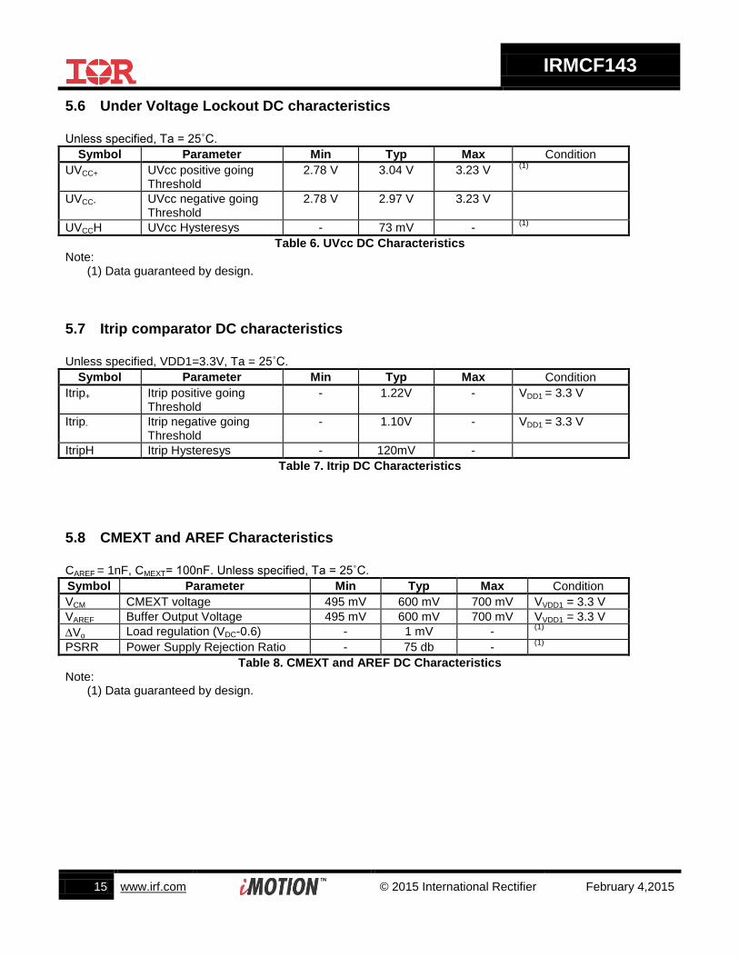
5.6 Under Voltage Lockout DC characteristics
Unless specified, Ta = 25˚C.
Symbol Parameter Min Typ Max Condition
UVCC+ UVcc positive going Threshold
2.78 V 3.04 V 3.23 V (1)
UVCC- UVcc negative going Threshold
2.78 V 2.97 V 3.23 V
UVCCH UVcc Hysteresys - 73 mV - (1)
Table 6. UVcc DC Characteristics Note:
(1) Data guaranteed by design.
5.7 Itrip comparator DC characteristics
Unless specified, VDD1=3.3V, Ta = 25˚C.
Symbol Parameter Min Typ Max Condition
Itrip+ Itrip positive going Threshold
- 1.22V - VDD1 = 3.3 V
Itrip- Itrip negative going Threshold
- 1.10V - VDD1 = 3.3 V
ItripH Itrip Hysteresys - 120mV -
Table 7. Itrip DC Characteristics
5.8 CMEXT and AREF Characteristics
CAREF = 1nF, CMEXT= 100nF. Unless specified, Ta = 25˚C.
Symbol Parameter Min Typ Max Condition
VCM CMEXT voltage 495 mV 600 mV 700 mV VVDD1 = 3.3 V
VAREF Buffer Output Voltage 495 mV 600 mV 700 mV VVDD1 = 3.3 V
Vo Load regulation (VDC-0.6) - 1 mV - (1)
PSRR Power Supply Rejection Ratio - 75 db - (1)
Table 8. CMEXT and AREF DC Characteristics Note:
(1) Data guaranteed by design.
IRMCF143
16 www.irf.com © 2015 International Rectifier February 4,2015
6 AC Characteristics
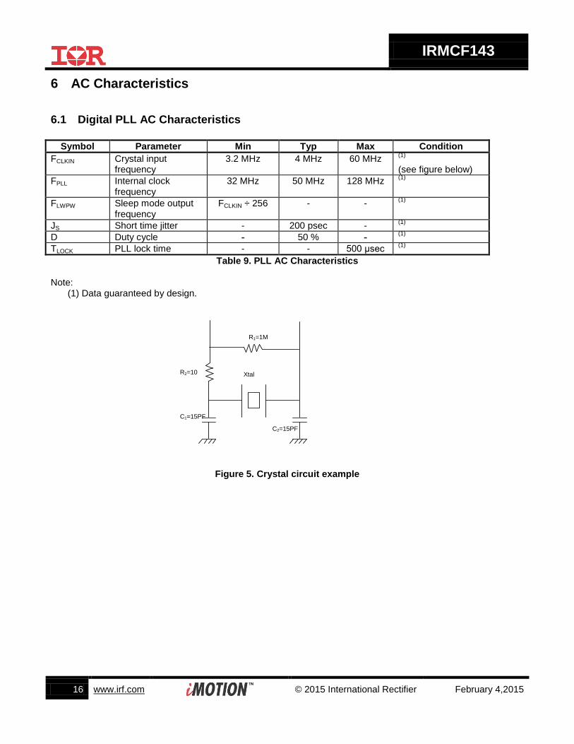
6.1 Digital PLL AC Characteristics
Symbol Parameter Min Typ Max Condition
FCLKIN Crystal input frequency
3.2 MHz 4 MHz 60 MHz (1)
(see figure below)
FPLL Internal clock frequency
32 MHz 50 MHz 128 MHz (1)
FLWPW Sleep mode output frequency
FCLKIN ÷ 256 - - (1)
JS Short time jitter - 200 psec - (1)
D Duty cycle - 50 % - (1)
TLOCK PLL lock time - - 500 μsec (1)
Table 9. PLL AC Characteristics Note:
(1) Data guaranteed by design.
Xtal
R1=1M
R2=10
C1=15PF
C2=15PF
Figure 5. Crystal circuit example
IRMCF143
17 www.irf.com © 2015 International Rectifier February 4,2015
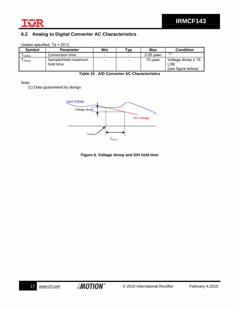
6.2 Analog to Digital Converter AC Characteristics
Unless specified, Ta = 25˚C.
Symbol Parameter Min Typ Max Condition
TCONV Conversion time - - 2.05 μsec (1)
THOLD Sample/Hold maximum hold time
- - 10 μsec Voltage droop ≤ 15 LSB (see figure below)
Table 10 . A/D Converter AC Characteristics Note:
(1) Data guaranteed by design.
THOLD
Voltage droop
tSAMPLE
S/H Voltage
Input Voltage
Figure 6. Voltage droop and S/H hold time
IRMCF143
18 www.irf.com © 2015 International Rectifier February 4,2015
6.3 Op amp AC Characteristics
Unless specified, Ta = 25˚C.
Symbol Parameter Min Typ Max Condition
OPSR OP amp slew rate - 10 V/μsec - VDD1 = 3.3 V, CL = 33 pF
(1)
OPIMP OP input impedance - 108 Ω -
(1) (2)
TSET Settling time - 400 ns - VDD1 = 3.3 V, CL = 33 pF
(1)
Table 11 Current Sensing OP Amp AC Characteristics Note:
(1) Data guaranteed by design. (2) To guarantee stability of the operational amplifier, it is recommended to load the output pin by a capacitor of 47pF, see Figure 7.
AVREFExternal
components
47pF
Figure 7. Op amp output capacitor
IRMCF143
19 www.irf.com © 2015 International Rectifier February 4,2015
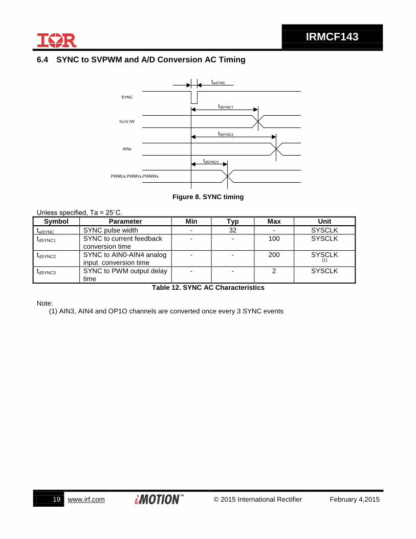
6.4 SYNC to SVPWM and A/D Conversion AC Timing
SYNC
IU,IV,IW
twSYNC
tdSYNC1
AINx
tdSYNC2
PWMUx,PWMVx,PWMWx
tdSYNC3
Figure 8. SYNC timing
Unless specified, Ta = 25˚C.
Symbol Parameter Min Typ Max Unit
twSYNC SYNC pulse width - 32 - SYSCLK
tdSYNC1 SYNC to current feedback conversion time
- - 100 SYSCLK
tdSYNC2 SYNC to AIN0-AIN4 analog input conversion time
- - 200 SYSCLK (1)
tdSYNC3 SYNC to PWM output delay time
- - 2 SYSCLK
Table 12. SYNC AC Characteristics Note:
(1) AIN3, AIN4 and OP1O channels are converted once every 3 SYNC events
IRMCF143
20 www.irf.com © 2015 International Rectifier February 4,2015
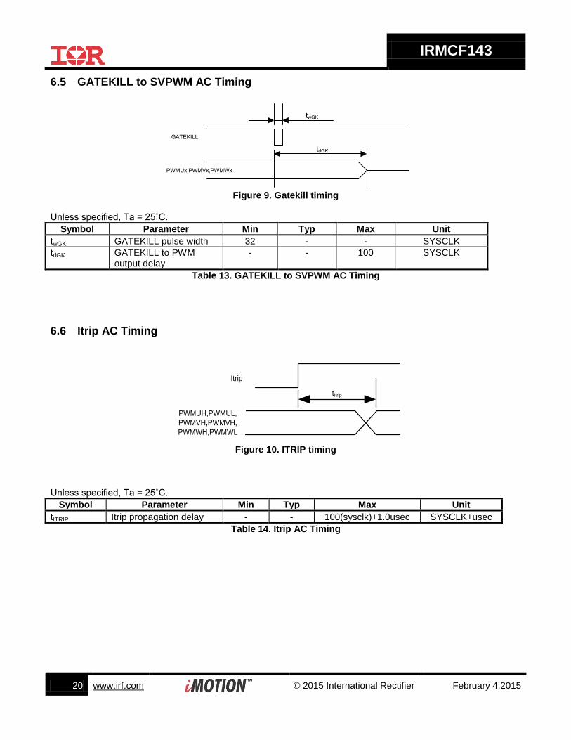
6.5 GATEKILL to SVPWM AC Timing
GATEKILL
PWMUx,PWMVx,PWMWx
twGK
tdGK
Figure 9. Gatekill timing
Unless specified, Ta = 25˚C.
Symbol Parameter Min Typ Max Unit
twGK GATEKILL pulse width 32 - - SYSCLK
tdGK GATEKILL to PWM output delay
- - 100 SYSCLK
Table 13. GATEKILL to SVPWM AC Timing
6.6 Itrip AC Timing
Itrip
PWMUH,PWMUL,
PWMVH,PWMVH,
PWMWH,PWMWL
tItrip
Figure 10. ITRIP timing
Unless specified, Ta = 25˚C.
Symbol Parameter Min Typ Max Unit
tITRIP Itrip propagation delay - - 100(sysclk)+1.0usec SYSCLK+usec
Table 14. Itrip AC Timing
IRMCF143
21 www.irf.com © 2015 International Rectifier February 4,2015
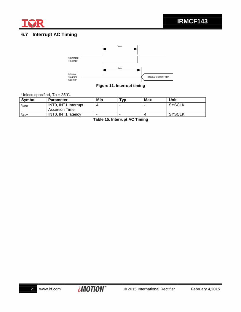
6.7 Interrupt AC Timing
P3.2/INT0
P3.3/INT1
Internal
Program
Counter
Internal Vector Fetch
twINT
tdINT
Figure 11. Interrupt timing
Unless specified, Ta = 25˚C.
Symbol Parameter Min Typ Max Unit
twINT INT0, INT1 Interrupt Assertion Time
4 - - SYSCLK
tdINT INT0, INT1 latency - - 4 SYSCLK
Table 15. Interrupt AC Timing
IRMCF143
22 www.irf.com © 2015 International Rectifier February 4,2015
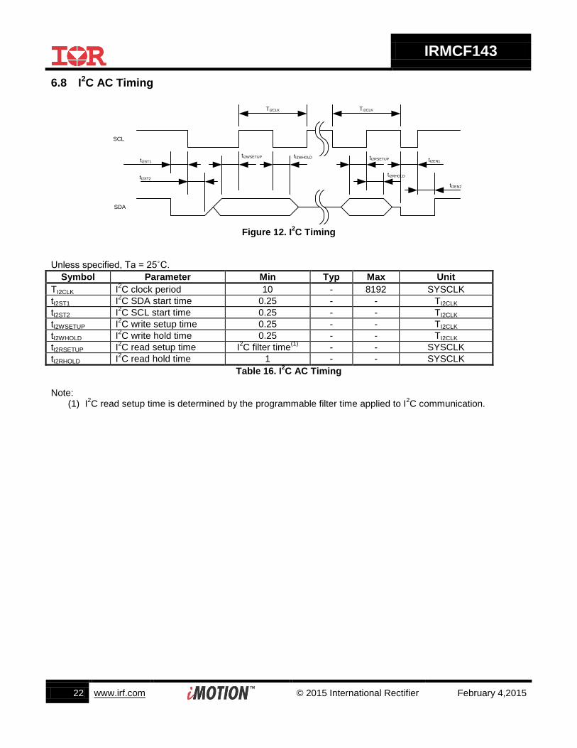
6.8 I2C AC Timing
SCL
SDA
tI2ST1
tI2ST2
tI2WSETUP
TI2CLK
tI2WHOLD tI2RSETUP
tI2RHOLD
TI2CLK
tI2EN1
tI2EN2
Figure 12. I
2C Timing
Unless specified, Ta = 25˚C.
Symbol Parameter Min Typ Max Unit
TI2CLK I2C clock period 10 - 8192 SYSCLK
tI2ST1 I2C SDA start time 0.25 - - TI2CLK
tI2ST2 I2C SCL start time 0.25 - - TI2CLK
tI2WSETUP I2C write setup time 0.25 - - TI2CLK
tI2WHOLD I2C write hold time 0.25 - - TI2CLK
tI2RSETUP I2C read setup time I
2C filter time
(1) - - SYSCLK
tI2RHOLD I2C read hold time 1 - - SYSCLK
Table 16. I2C AC Timing
Note:
(1) I2C read setup time is determined by the programmable filter time applied to I
2C communication.
IRMCF143
23 www.irf.com © 2015 International Rectifier February 4,2015
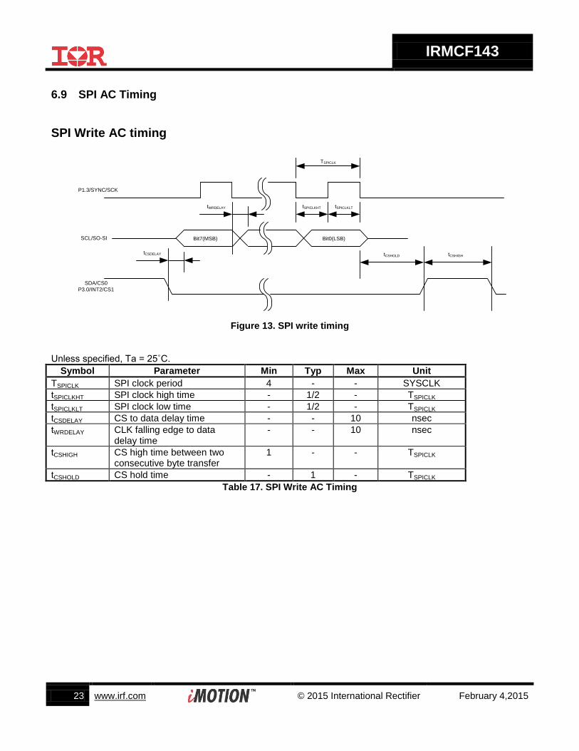
6.9 SPI AC Timing
SPI Write AC timing
P1.3/SYNC/SCK
SCL/SO-SI
TSPICLK
tWRDELAY
tCSHOLD
SDA/CS0
P3.0/INT2/CS1
tCSHIGH
Bit7(MSB) Bit0(LSB)
tSPICLKHT tSPICLKLT
tCSDELAY
Figure 13. SPI write timing
Unless specified, Ta = 25˚C.
Symbol Parameter Min Typ Max Unit
TSPICLK SPI clock period 4 - - SYSCLK
tSPICLKHT SPI clock high time - 1/2 - TSPICLK
tSPICLKLT SPI clock low time - 1/2 - TSPICLK
tCSDELAY CS to data delay time - - 10 nsec
tWRDELAY CLK falling edge to data delay time
- - 10 nsec
tCSHIGH CS high time between two consecutive byte transfer
1 - - TSPICLK
tCSHOLD CS hold time - 1 - TSPICLK
Table 17. SPI Write AC Timing
IRMCF143
24 www.irf.com © 2015 International Rectifier February 4,2015
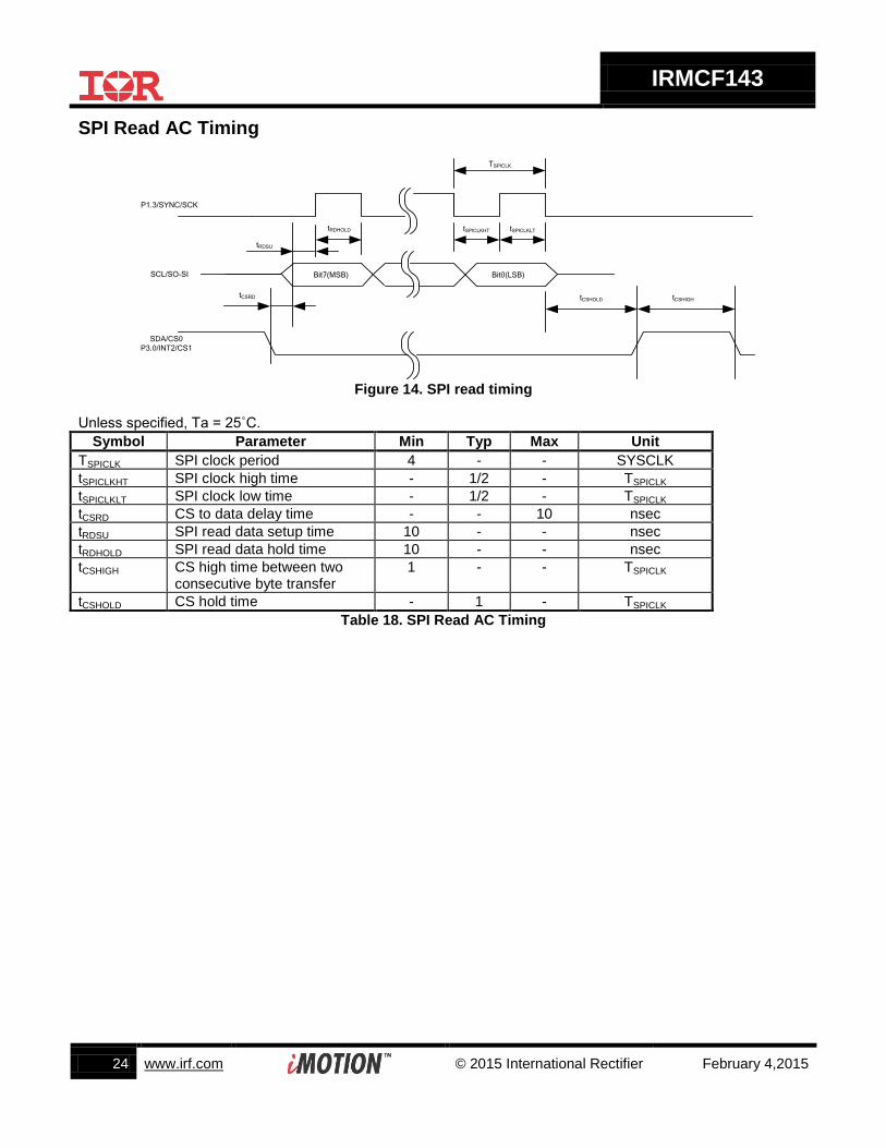
SPI Read AC Timing
P1.3/SYNC/SCK
SCL/SO-SI
TSPICLK
tRDSU
tCSHOLD
SDA/CS0
P3.0/INT2/CS1
tCSHIGH
Bit7(MSB) Bit0(LSB)
tSPICLKHT tSPICLKLT
tCSRD
tRDHOLD
Figure 14. SPI read timing
Unless specified, Ta = 25˚C.
Symbol Parameter Min Typ Max Unit
TSPICLK SPI clock period 4 - - SYSCLK
tSPICLKHT SPI clock high time - 1/2 - TSPICLK
tSPICLKLT SPI clock low time - 1/2 - TSPICLK
tCSRD CS to data delay time - - 10 nsec
tRDSU SPI read data setup time 10 - - nsec
tRDHOLD SPI read data hold time 10 - - nsec
tCSHIGH CS high time between two consecutive byte transfer
1 - - TSPICLK
tCSHOLD CS hold time - 1 - TSPICLK
Table 18. SPI Read AC Timing

IRMCF143
25 www.irf.com © 2015 International Rectifier February 4,2015
6.10 UART AC Timing
TXD
RXD
Data and Parity BitStart Bit
TBAUD
Stop Bit
TUARTFIL
Figure 15. UART timing
Unless specified, Ta = 25˚C.
Symbol Parameter Min Typ Max Unit
TBAUD Baud Rate Period - 57600 - bit/sec
TUARTFIL UART sampling filter period
(1)
- 1/16 - TBAUD
Table 19. UART AC Timing Note:
(1) Each bit including start and stop bit is sampled three times at center of a bit at an interval of 1/16 TBAUD. If three sampled values do not agree, then UART noise error is generated.
IRMCF143
26 www.irf.com © 2015 International Rectifier February 4,2015
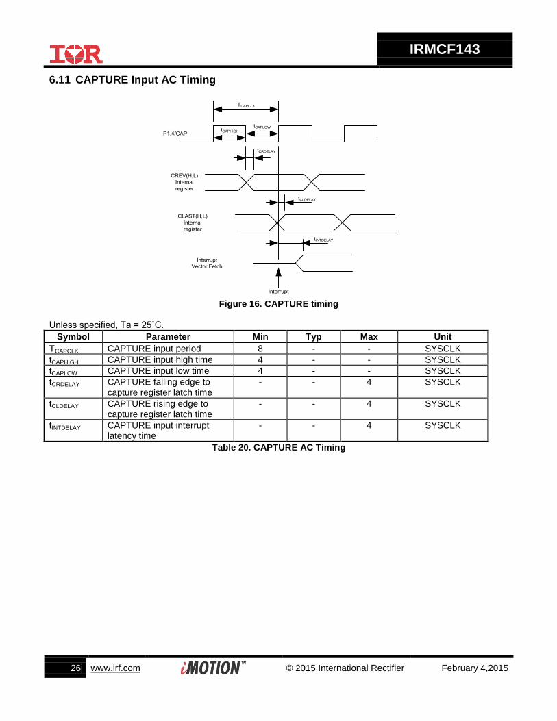
6.11 CAPTURE Input AC Timing
P1.4/CAP
CREV(H,L)
Internal
register
tCAPHIGH
TCAPCLK
tCRDELAY
tCAPLOW
tCLDELAY
CLAST(H,L)
Internal
register
tINTDELAY
Interrupt
Vector Fetch
Interrupt
Figure 16. CAPTURE timing Unless specified, Ta = 25˚C.
Symbol Parameter Min Typ Max Unit
TCAPCLK CAPTURE input period 8 - - SYSCLK
tCAPHIGH CAPTURE input high time 4 - - SYSCLK
tCAPLOW CAPTURE input low time 4 - - SYSCLK
tCRDELAY CAPTURE falling edge to capture register latch time
- - 4 SYSCLK
tCLDELAY CAPTURE rising edge to capture register latch time
- - 4 SYSCLK
tINTDELAY CAPTURE input interrupt latency time
- - 4 SYSCLK
Table 20. CAPTURE AC Timing
IRMCF143
27 www.irf.com © 2015 International Rectifier February 4,2015
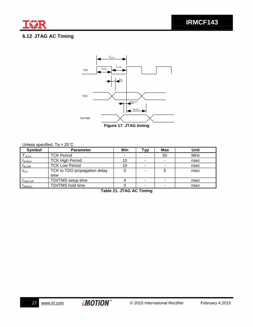
6.12 JTAG AC Timing
TCK
TDO
tJHIGH
TJCLK
tCO
tJLOW
tJSETUP
tJHOLD
TDI/TMS
Figure 17. JTAG timing
Unless specified, Ta = 25˚C.
Symbol Parameter Min Typ Max Unit
TJCLK TCK Period - - 50 MHz
tJHIGH TCK High Period 10 - - nsec
tJLOW TCK Low Period 10 - - nsec
tCO TCK to TDO propagation delay time
0 - 5 nsec
tJSETUP TDI/TMS setup time 4 - - nsec
tJHOLD TDI/TMS hold time 0 - - nsec
Table 21. JTAG AC Timing
IRMCF143
28 www.irf.com © 2015 International Rectifier February 4,2015
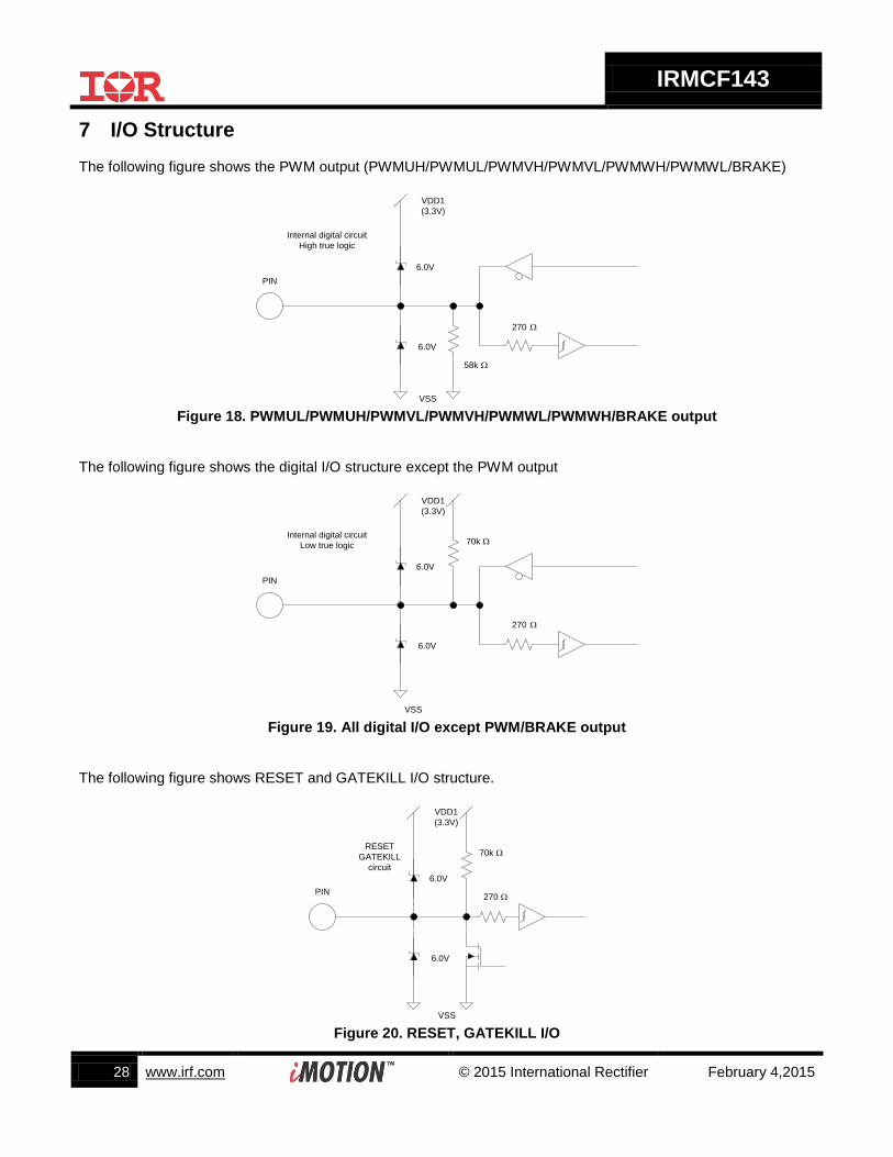
7 I/O Structure The following figure shows the PWM output (PWMUH/PWMUL/PWMVH/PWMVL/PWMWH/PWMWL/BRAKE)
270
6.0V
6.0V
Internal digital circuit
High true logic
VDD1
(3.3V)
VSS
58k
PIN
Figure 18. PWMUL/PWMUH/PWMVL/PWMVH/PWMWL/PWMWH/BRAKE output
The following figure shows the digital I/O structure except the PWM output
6.0V
6.0V
Internal digital circuit
Low true logic
VDD1
(3.3V)
70k
PIN
VSS
270
Figure 19. All digital I/O except PWM/BRAKE output
The following figure shows RESET and GATEKILL I/O structure.
270
6.0V
6.0V
RESET
GATEKILL
circuit
VDD1
(3.3V)
70k
PIN
VSS Figure 20. RESET, GATEKILL I/O
IRMCF143
29 www.irf.com © 2015 International Rectifier February 4,2015
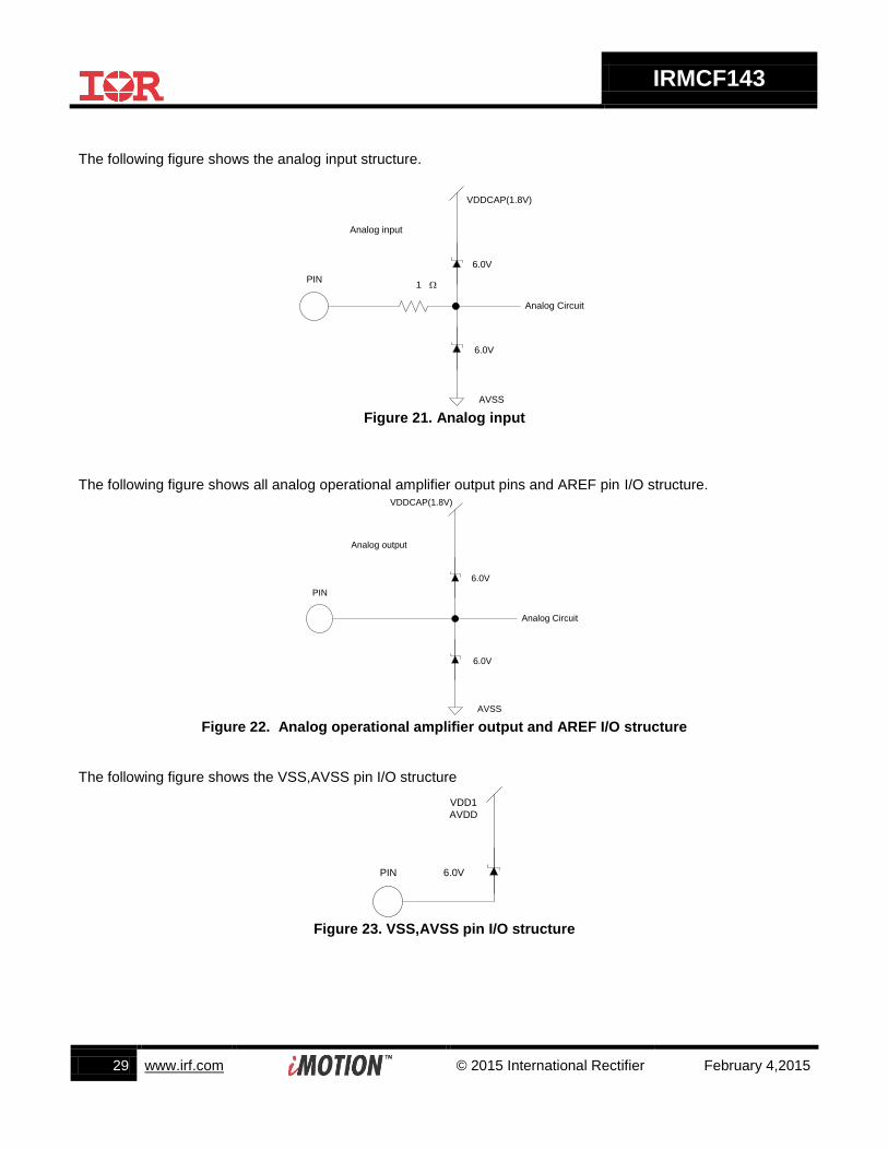
The following figure shows the analog input structure.
1
6.0V
6.0V
Analog input
PIN
AVSS
Analog Circuit
VDDCAP(1.8V)
Figure 21. Analog input
The following figure shows all analog operational amplifier output pins and AREF pin I/O structure.
6.0V
6.0V
Analog output
PIN
AVSS
Analog Circuit
VDDCAP(1.8V)
Figure 22. Analog operational amplifier output and AREF I/O structure
The following figure shows the VSS,AVSS pin I/O structure
PIN
VDD1
AVDD
6.0V
Figure 23. VSS,AVSS pin I/O structure

IRMCF143
30 www.irf.com © 2015 International Rectifier February 4,2015
The following figure shows the VDD1,VDDCAP pin I/O structure
PIN
VSS
6.0V
Figure 24. VDD1,VDDCAP pin I/O structure
The following figure shows the XTAL0 and XTAL1 pins structure
1
6.0V
6.0V
PIN
VSS
VDDCAP(1.8V)
Figure 25. XTAL0/XTAL1 pins structure

IRMCF143
31 www.irf.com © 2015 International Rectifier February 4,2015
8 Pin List
Pin Number
Pin Name
Internal Pull-up / down
Pin Type
Description
1 XTAL0 -- I Crystal input
2 XTAL1 -- O Crystal output
3 P1.0/PULSE/T2/MT1
-- I/O Discrete programmable I/O or Pulse Input or Timer/Counter 2 input or MCE Pin Timer 1
4 SCL/SO-SI -- I/O I2C clock output (open drain, need pull up) or SPI data
5 SDA/CS0 -- I/O I2C data (open drain, need pull up) or SPI Chip Select
0
6 P1.3/SYNC/SCK -- I/O Discrete programmable I/O or SYNC output or SPI clock output
7 P1.4/ENC-A -- I/O Discrete programmable I/O or Encoder A input
8 P1.6/ENC-B -- I/O Discrete programmable I/O or Encoder B input
9 P1.7/ENC-C -- I/O Discrete programmable I/O or Encoder C input
10 VDD1 -- P 3.3V digital power
11 VSS -- P Digital common
12 VDDCAP -- P Internal 1.8V output, Capacitor(s) to be connected
13 P2.0/DIR/NMI -- I/O Discrete programmable I/O or DIR input or Non-maskable Interrupt input
14 P3.2/INT0 -- I/O Discrete programmable I/O or Interrupt 0 input
15 P2.2/CAP -- I/O Discrete programmable I/O or Capture Timer input
16 P2.3/MATCH -- I/O Discrete programmable I/O or MATCH output
17 P2.5/INT2 -- I/O Discrete programmable I/O or Interrupt 2 input
18 P2.6/AO0 -- I/O Discrete programmable I/O or PWM 0 digital output
19 P2.7/AO1/MT2 -- I/O Discrete programmable I/O or PWM 1 digital output or MCE pin timer 2 output
20 OP1O -- O Op amp output for application sensing, 0-1.2V range
21 OP1- -- I Op amp negative input for application sensing, 0-1.2V range, needs to be pulled down to AVSS if unused
22 OP1+ -- I Op amp positive input for application sensing, 0-1.2V range, needs to be pulled down to AVSS if unused
23 VDCBUS -- I Analog input channel (0 – 1.2V), allocated by MCE for DC bus voltage input
24 AIN1 -- I Analog input channel 1, 0-1.2V range, allocated by MCE as speed input, needs to be pulled down to
AVSS if unused
25 AIN2 -- I Analog input channel 2, 0-1.2V range, allocated by MCE as torque input, needs to be pulled down to
AVSS if unused
26 AIN3 -- I Analog input channel 3, 0-1.2V range, needs to be pulled down to AVSS if unused
27 AIN4 -- I Analog input channel 4, 0-1.2V range, needs to be pulled down to AVSS if unused
28 IFBU- -- I Op amp negative input for U phase current sensing, 0-1.2V range
29 IFBU+ -- I Op amp positive input for U phase current sensing, 0-1.2V range
30 IFBUO -- O Op amp output for U phase current sensing, 0-1.2V range
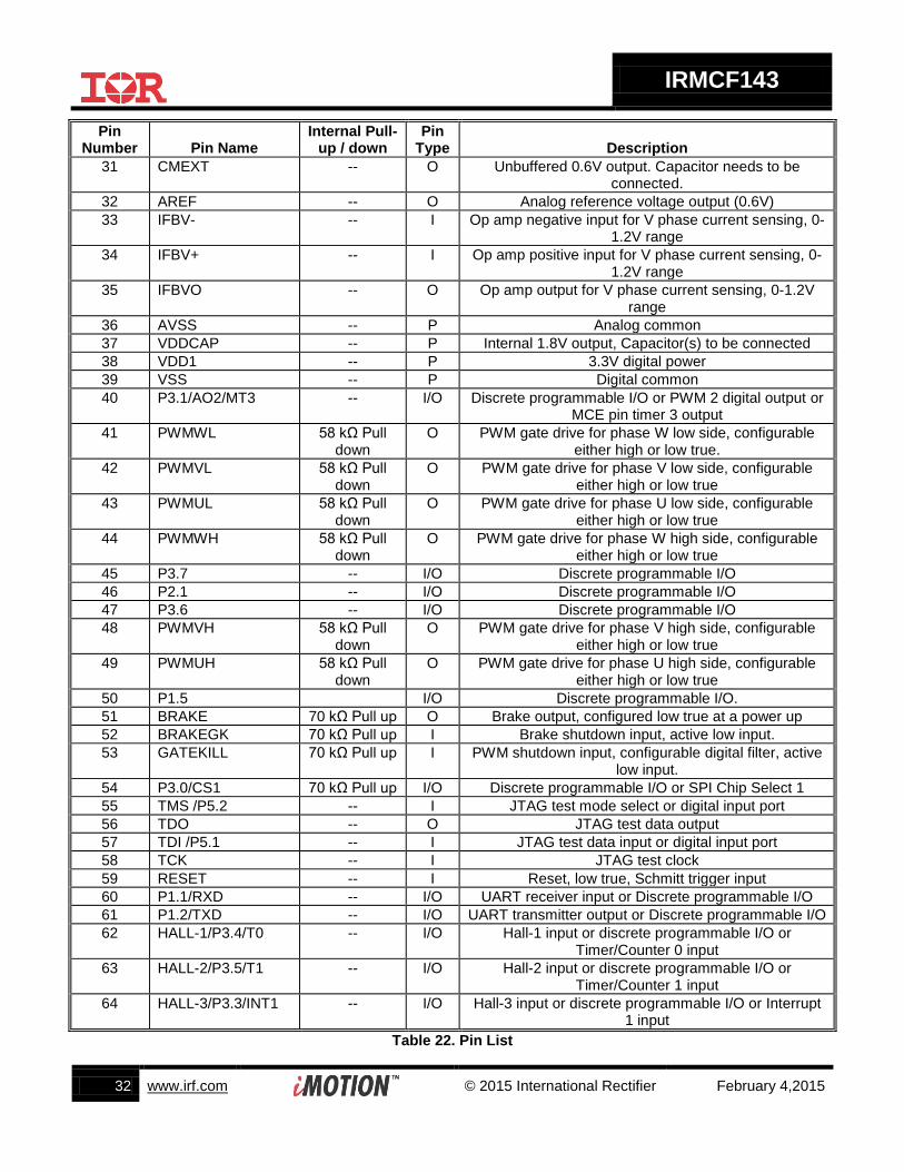
IRMCF143
32 www.irf.com © 2015 International Rectifier February 4,2015
Pin Number
Pin Name
Internal Pull-up / down
Pin Type
Description
31 CMEXT -- O Unbuffered 0.6V output. Capacitor needs to be connected.
32 AREF -- O Analog reference voltage output (0.6V)
33 IFBV- -- I Op amp negative input for V phase current sensing, 0-1.2V range
34 IFBV+ -- I Op amp positive input for V phase current sensing, 0-1.2V range
35 IFBVO -- O Op amp output for V phase current sensing, 0-1.2V range
36 AVSS -- P Analog common
37 VDDCAP -- P Internal 1.8V output, Capacitor(s) to be connected
38 VDD1 -- P 3.3V digital power
39 VSS -- P Digital common
40 P3.1/AO2/MT3 -- I/O Discrete programmable I/O or PWM 2 digital output or MCE pin timer 3 output
41 PWMWL 58 kΩ Pull down
O PWM gate drive for phase W low side, configurable either high or low true.
42 PWMVL 58 kΩ Pull down
O PWM gate drive for phase V low side, configurable either high or low true
43 PWMUL 58 kΩ Pull down
O PWM gate drive for phase U low side, configurable either high or low true
44 PWMWH 58 kΩ Pull down
O PWM gate drive for phase W high side, configurable either high or low true
45 P3.7 -- I/O Discrete programmable I/O
46 P2.1 -- I/O Discrete programmable I/O
47 P3.6 -- I/O Discrete programmable I/O
48 PWMVH 58 kΩ Pull down
O PWM gate drive for phase V high side, configurable either high or low true
49 PWMUH 58 kΩ Pull down
O PWM gate drive for phase U high side, configurable either high or low true
50 P1.5 I/O Discrete programmable I/O.
51 BRAKE 70 kΩ Pull up O Brake output, configured low true at a power up
52 BRAKEGK 70 kΩ Pull up I Brake shutdown input, active low input.
53 GATEKILL 70 kΩ Pull up I PWM shutdown input, configurable digital filter, active low input.
54 P3.0/CS1 70 kΩ Pull up I/O Discrete programmable I/O or SPI Chip Select 1
55 TMS /P5.2 -- I JTAG test mode select or digital input port
56 TDO -- O JTAG test data output
57 TDI /P5.1 -- I JTAG test data input or digital input port
58 TCK -- I JTAG test clock
59 RESET -- I Reset, low true, Schmitt trigger input
60 P1.1/RXD -- I/O UART receiver input or Discrete programmable I/O
61 P1.2/TXD -- I/O UART transmitter output or Discrete programmable I/O
62 HALL-1/P3.4/T0 -- I/O Hall-1 input or discrete programmable I/O or Timer/Counter 0 input
63 HALL-2/P3.5/T1 -- I/O Hall-2 input or discrete programmable I/O or Timer/Counter 1 input
64 HALL-3/P3.3/INT1 -- I/O Hall-3 input or discrete programmable I/O or Interrupt 1 input
Table 22. Pin List
IRMCF143
33 www.irf.com © 2015 International Rectifier February 4,2015
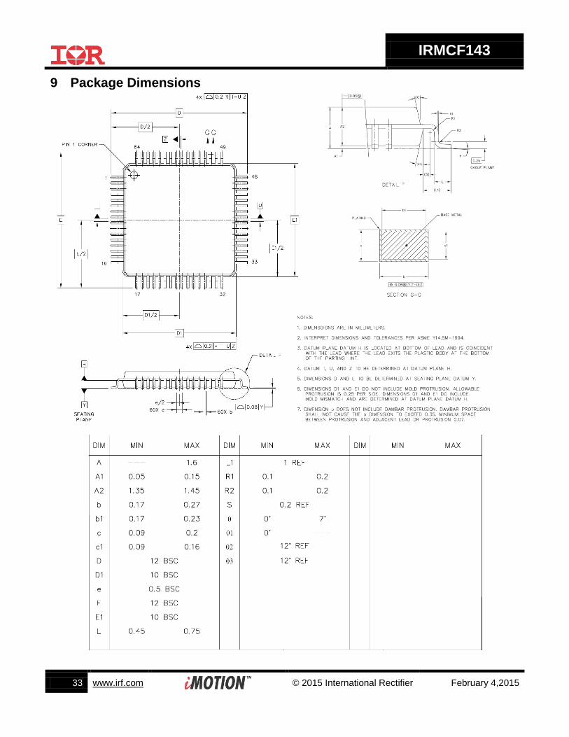
9 Package Dimensions
IRMCF143
34 www.irf.com © 2015 International Rectifier February 4,2015
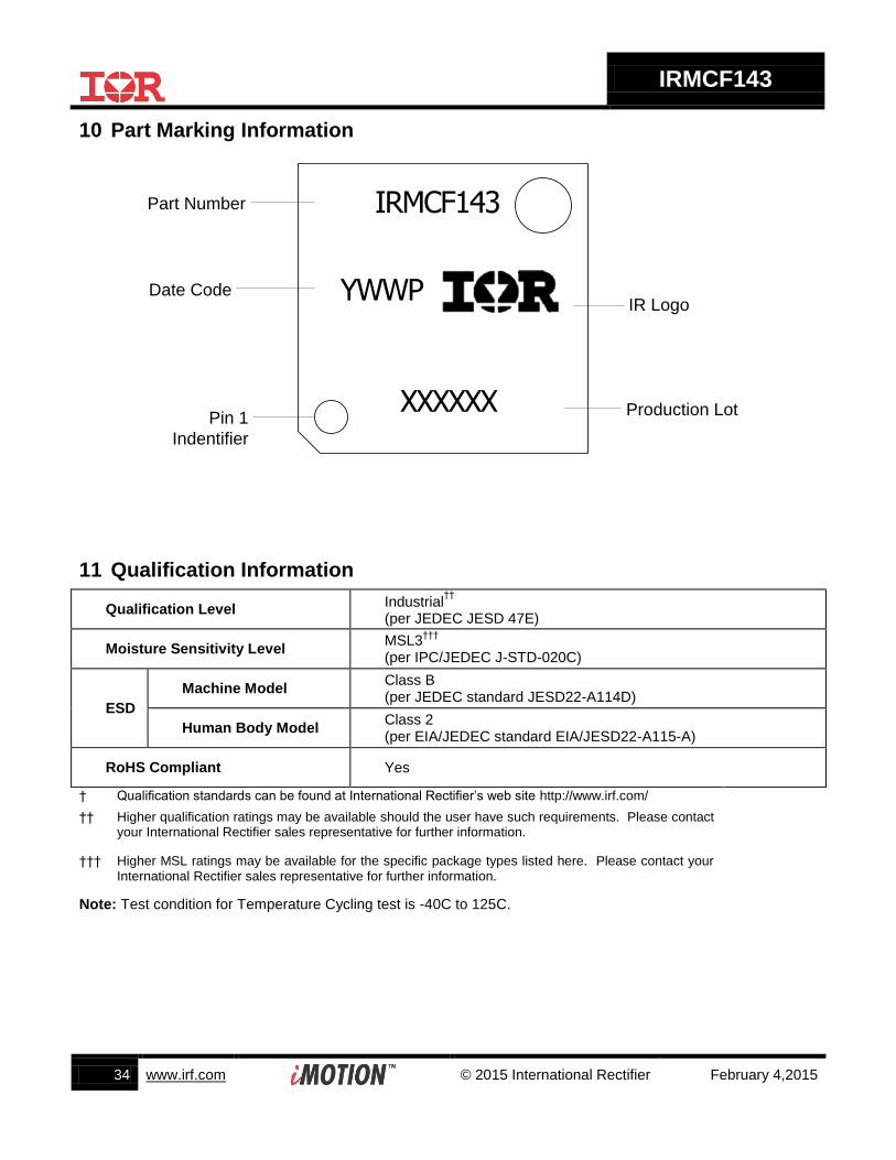
10 Part Marking Information
IRMCF143
YWWP
XXXXXX
IR Logo
Production Lot
Date Code
Part Number
Pin 1
Indentifier
11 Qualification Information
Qualification Level Industrial
††
(per JEDEC JESD 47E)
Moisture Sensitivity Level MSL3
†††
(per IPC/JEDEC J-STD-020C)
ESD
Machine Model Class B (per JEDEC standard JESD22-A114D)
Human Body Model Class 2 (per EIA/JEDEC standard EIA/JESD22-A115-A)
RoHS Compliant Yes
† Qualification standards can be found at International Rectifier’s web site http://www.irf.com/
†† Higher qualification ratings may be available should the user have such requirements. Please contact your International Rectifier sales representative for further information.
††† Higher MSL ratings may be available for the specific package types listed here. Please contact your International Rectifier sales representative for further information.
Note: Test condition for Temperature Cycling test is -40C to 125C.
IRMCF143
35 www.irf.com © 2015 International Rectifier February 4,2015
Revision History
Data and Specifications are subject to change without notice
IR WORLD HEADQUARTERS: 233 Kansas St., El Segundo, California 90245, USA Tel: (310) 252-7105 TAC Fax: (310) 252-7903
Visit us at www.irf.com for sales contact information