high performance filter and variable gain amplifier …cj82k9125/...high performance filter and...
TRANSCRIPT

High Performance Filter and Variable Gain Amplifier
Design for Biosignal Measurement Devices
A Thesis Presented
by
Kainan Wang
to
The Department of Electrical and Computer Engineering
in partial fulfillment of the requirement
for the degree of
Master of Science
in
Electrical Engineering
Northeastern University
Boston, Massachusetts
December, 2015

I
Abstract
In recent years, integrated circuits (ICs) for biosignal acquisitions have gained
popularity in both academia and the industry due to the rising demands in medical
applications. Biosignals such as brain signals monitored during electroencephalography
(EEG) tests can have very low signal levels down to a few microvolts. Therefore, a
biosignal measurement system usually requires multiple stages of amplification and
filtering to extract the signal of interest from noise and interference. The need to improve
the quality of the signal after processing in the analog front-end leads to circuit design
challenges that are addressed in this thesis.
The focus of this research is on the design of a low-pass notch filter (LPNF) and a
variable gain amplifier (VGA), which are both integrated into a Self-Calibrated Analog
Front-End for Long Acquisitions of Biosignals (SCAFELAB) system. The circuits were
designed, simulated and fabricated in 0.13-µm complementary metal-oxide semiconduc-
tor (CMOS) technology. Post-layout simulations of the LPNF show a passband
attenuation of 2.08 dB, a bandwidth of 47.2 Hz, and a 60.9 dB notch depth at 60 Hz to
reject powerline interference. The filter’s total input-referred noise integrated from 0.1
Hz to 47.2 Hz is 138.6 μV. Its simulated third-order harmonic distortion (HD3) with the
highest anticipated input amplitude is 61.1 dB. The post-layout simulations of the VGA
demonstrate a gain range of 32.2-51.3 dB with seven steps. The VGA’s total input-
referred noise integrated from 0.1 Hz to 47.2 Hz is 30.8 μV. Its HD3 is 80.8 dB with the
lowest gain setting and a 1 Vpk-pk output swing. Measurements of the complete analog
front-end chip (signal path blocks: instrumentation amplifier, LPNF and VGA) reveal a
differential gain range of 66-93 dB with a total power consumption of 41.59 µW. The
front-end bandwidth covers 0.5-40 Hz for EEG target applications, and its integrated
input-referred noise over the bandwidth is 3.75 µVrms. The measured third-order harmon-
ic distortion component is at least 57 dB below the fundamental signal level. A common-
mode rejection ratio (CMRR) of 77.6 dB and a power supply rejection ratio (PSRR) of
74 dB were measured at 10 Hz.

II
Acknowledgements
First and foremost, I would like to thank my family, who supported and encour-
aged me throughout the graduate study. I would like to thank my thesis advisor, Prof.
Marvin Onabajo, for his guidance on research and life. I would also like to thank my
committee members, Prof. Nian X. Sun and Prof. Mark Niedre, for their guidance
through the final stages of my M.S. degree completion. I thank the National Science
Foundation for financial support of the SCAFELAB project.
I would like to thank Li Xu and Chun-hsiang Chang for their help and guidance on
the all kinds of problems during the research process. I would like to thank Alireza
Zahrai, Li Xu, and Chun-hsiang Chang for collaborating on the SCAFELAB project.
Finally, to all of my friends all over the world, thank you for your encouragement
and care.

III
Table of Contents
Abstract ............................................................................................................................... I
Acknowledgements ............................................................................................................ II
1. INTRODUCTION ....................................................................................................... 1
1.1 BACKGROUND: BIOSIGNAL ACQUISITION CIRCUITS .......................... 1
1.1.1 Low-Transconductance OTA Design .................................................... 2
1.1.2 MOSFET Pseudo-Resistor Configuration.............................................. 3
1.1.3 Low Noise Design Consideration .......................................................... 4
1.2 SCAFELAB PROJECT SCOPE ........................................................................ 4
1.3 CONTRIBUTION OF THIS WORK ................................................................ 6
1.4 OUTLINE OF THE THESIS ............................................................................. 6
2. OVERVIEW: FILTERS .............................................................................................. 7
2.1 FILTER CLASSIFICATIONS........................................................................... 7
2.2 FILTER IMPLEMENTATIONS ....................................................................... 8
2.2.1 Passive Filters ........................................................................................ 8
2.2.2 Active Filters .......................................................................................... 9
3. LOW-PASS NOTCH FILTER DESIGN .................................................................. 11
3.1 INTRODUCTION ........................................................................................... 11
3.2 PRELIMINARY DESIGN WITH AN OTA MACRO-MODEL .................... 12
3.2.1 Passive Element Implementation ......................................................... 12
3.2.2 Macro-Model Implementation ............................................................. 13
3.3 OTA DESIGN .................................................................................................. 15
3.3.1 Low Transconductance Gain Realization ............................................ 15
3.3.2 Noise Optimization .............................................................................. 16
3.3.3 Linearity Optimization ......................................................................... 16
3.4 COMMON-MODE FEEDBACK DESIGN .................................................... 17
3.5 FABRICATED FILTER VERSION ................................................................ 18

IV
3.6 SIMULATION RESULTS .............................................................................. 20
4. VARIABLE GAIN AMPLIFIER (VGA) DESIGN .................................................. 26
4.1 INTRODUCTION ........................................................................................... 26
4.2 VGA Design ..................................................................................................... 26
4.3 OTA DESIGN .................................................................................................. 28
4.4 COMMON-MODE FEEDBACK CIRCUIT ................................................... 29
4.5 PSEUDO-RESISTOR ...................................................................................... 29
4.6 FABRICATED VGA VERSION ..................................................................... 30
4.7 SIMULATION RESULTS .............................................................................. 31
5. ANALOG FRONT-END SIMULATION RESULTS............................................... 36
5.1 SIMULATED FREQUENCY RESPONSE OF THE COMPLETE ANALOG
FRONT-END ................................................................................................... 36
5.2 DISTORTION SMULATION ......................................................................... 38
5.3 NOISE SIMULATION .................................................................................... 39
5.4 SMULATION WITH A COMMON-MODE INPUT SIGNAL ...................... 40
5.5 SMULATION WITH POWERLINE INTERFERENCE ................................ 41
6. PROTOTYPE CHIP AND PRINTED CIRCUIT BOARD DESIGN ....................... 43
6.1 FABRICATED CHIP ...................................................................................... 43
6.2 PCB DESIGN .................................................................................................. 45
6.3 MEASUREMENT SETUP AND TEST DESCRIPTIONS ............................. 46
6.3.1 Gain Measurement ............................................................................... 47
6.3.2 Nonlinearity Measurement ................................................................... 48
6.3.3 Noise Measurement .............................................................................. 49
6.3.4 CMRR Measurement ........................................................................... 50
6.3.5 PSRR Measurement ............................................................................. 52
6.4 MEASUREMENT RESULTS AND DISCUSSION ....................................... 53
6.4.1 LPNF Tuning ....................................................................................... 53
6.4.2 Gain Measurement Results .................................................................. 55

V
6.4.3 Noise Measurement Result .................................................................. 60
6.4.4 Distortion Measurement ....................................................................... 62
6.4.5 CMRR Measurement Result ................................................................ 64
6.4.6 PSRR Measurement Result .................................................................. 64
6.4.7 Measurement Summary ....................................................................... 65
7. CONCLUSION AND FUTURE WORK .................................................................. 68
REFERENCES ................................................................................................................ 69
APPENDIX...................................................................................................................... 74

VI
List of Figures
Fig. 1 Emotiv EPOC EEG headset .................................................................................... 1
Fig. 2 (a) PMOS pseudo-resistors with voltage tunability, (b) PMOS-bipolar pseudo-
resistors, (c) oppositely-connected PMOS-bipolar pseudo-resistors. ................................ 3
Fig. 3 Analog front-end for EEG signal measurements with electrode cable capacitances
and calibration blocks for input impedance boosting. ....................................................... 5
Fig. 4 Transfer functions of a low-pass filter (upper left), band-pass filter (upper right),
high-pass filter (lower left) and band-stop filter (lower right). ......................................... 7
Fig. 5 Example transfer functions: three types of fifth-order low-pass filters. .................. 8
Fig. 6 A fifth-order RLC Butterworth filter....................................................................... 8
Fig. 7 OTA-C based (a) inductor and (b) resistor. ........................................................... 10
Fig. 8 Diagram of fully-differential analog front-end for biosignal measurements. ....... 12
Fig. 9 An elliptic filter built with passive components. ................................................... 12
Fig. 10 Fifth-order single-ended low-pass notch filter (LPNF). ...................................... 13
Fig. 11 OTA macro-model. ............................................................................................. 14
Fig. 12 Fifth-order fully-differential low-pass notch filter (LPNF). ............................... 14
Fig. 13 OTA with differential difference input stage. ..................................................... 15
Fig. 14 Common-mode feedback amplifier. .................................................................... 17
Fig. 15 Frequency response of one CMFB loop. ............................................................. 18
Fig. 16 Layout of one OTA in the LPNF......................................................................... 19
Fig. 17 Layout of the complete LPNF. ............................................................................ 19
Fig. 18 Frequency response of the LPNF. ....................................................................... 21
Fig. 19 Simulated input-referred noise spectral density of the LPNF. ............................ 22
Fig. 20 Transient output voltage of the LPNF with 30 mVpk-pk input @ 10 Hz. ............. 22
Fig. 21 Output voltage spectrum of the LPNF with 30 mVpk-pk input @ 10 Hz. ............. 23
Fig. 22 CMRR (top) and PSRR (bottom) results for the LPNF (from 200 Monte Carlo
runs). ................................................................................................................................ 24
Fig. 23 LPNF frequency responses from Monte Carlo simulations: worst cases before
tuning (solid lines) and after tuning (dashed lines). ........................................................ 25
Fig. 24 Variable gain amplifier with three-bit control. .................................................... 26
Fig. 25 Capacitor bank in the VGA. ................................................................................ 27

VII
Fig. 26 Complete VGA block diagram. ........................................................................... 28
Fig. 27 Schematic of the OTA for the VGA. ................................................................... 28
Fig. 28 A pseudo-resistor implemented with PMOS transistors. .................................... 30
Fig. 29 Layout of the 2-stage VGA. ................................................................................ 31
Fig. 30 Frequency response of the VGA. ........................................................................ 32
Fig. 31 Simulated input-referred noise spectral density of the VGA. ............................. 33
Fig. 32 Transient differential output voltage of the VGA with 25 mVpk-pk input @ 10 Hz.
......................................................................................................................................... 33
Fig. 33 Output voltage spectrum of the VGA with 25 mVpk-pk input @ 10 Hz. .............. 34
Fig. 34 CMRR and PSRR results for the VGA (from 200 Monte Carlo runs). ............... 35
Fig. 35 Simulated AFE gain with (a) 30 dB, (b) 40 dB, and (c) 50 dB IA gain settings. 37
Fig. 36 AFE output voltage spectrum with differential 200 µVpk-pk input at 5 Hz (AFE gain
= 74.6 dB). ....................................................................................................................... 38
Fig. 37 AFE output voltage spectrum with differential 600 µVpk-pk input at 5 Hz (AFE gain
= 61.2 dB). ....................................................................................................................... 39
Fig. 38 Output noise density vs. frequency of the AFE system with gain of 71.2 dB. ... 39
Fig. 39 Differential output voltage of the AFE with a 5 mVpk-pk common-mode input at
10 Hz. ............................................................................................................................... 40
Fig. 40 Differential output voltage of the IA with 5 mVpk-pk common-mode input at 10
Hz. .................................................................................................................................... 41
Fig. 41 Differential output voltage of the AFE with a 5 mVpk-pk sinusoidal signal at 10 Hz
coupled to the power supply of the complete AFE (red line) and only to the supply of the
IA and VGA (blue line). ................................................................................................... 42
Fig. 42 SCAFELAB chip layout. ..................................................................................... 43
Fig. 43 Chip micrograph of the fabricated EEG front-end with input impedance boosting
capability in IBM 0.13µm CMOS technology and zoomed-in analog front-end. ........... 44
Fig. 44 SCAFELAB PCB photo. ..................................................................................... 45
Fig. 45 Systematic gain measurement setup. ................................................................... 47
Fig. 46 Nonlinearity measurement setup. ........................................................................ 48
Fig. 47 Noise measurement setup. ................................................................................... 49
Fig. 48 CMRR test bench in general. .............................................................................. 50

VIII
Fig. 49 CMRR measurement setup. ................................................................................. 51
Fig. 50 PSRR measurement setup. .................................................................................. 52
Fig. 51 Complete measurement setup on the bench. ....................................................... 53
Fig. 52 Frequency response of the analog front-end before filter tuning. ....................... 54
Fig. 53 Frequency response of the analog front-end after filter tuning. .......................... 55
Fig. 54 AFE frequency responses for the 14 gain settings with 40 dB input attenuation
and 6 dB driver gain of the test setup. ............................................................................. 56
Fig. 55 AFE frequency responses with IA in high gain mode and de-embedded test setup
gain/attenuation. ............................................................................................................... 57
Fig. 56 AFE frequency responses with IA in low gain mode and de-embedded test setup
gain/attenuation. ............................................................................................................... 57
Fig. 57 Frequency response with the lowest AFE gain setting over wide frequency range.
......................................................................................................................................... 58
Fig. 58 Measured transient output voltage of the AFE with 500 µVpk input at 5 Hz using
the lowest gain mode. ...................................................................................................... 59
Fig. 59 Measured transient output voltage of the AFE with 10 µVpk input at 5 Hz using
the maximum gain mode. ................................................................................................ 60
Fig. 60 FFT of the AFE output voltage with the same test condition as in Fig. 59. ........ 60
Fig. 61 Output-referred noise measurement of the complete EEG front-end. ................. 61
Fig. 62 Distortion measurement with a 200 µVpk-pk input at 5 Hz (with 75 dB gain). .... 63
Fig. 63 Distortion measurement with a 600 µVpk-pk input at 5 Hz (with 66 dB gain). .... 63
Fig. 64 Differential output voltage of the AFE with a common-mode input sinusoidal
signal of 5 mVpk-pk at 10 Hz. ............................................................................................ 64
Fig. 65 Differential output voltage of the AFE with a sinusoidal input signal of 5 mVpk-pk
at 10 Hz coupled to the power supply voltage. ................................................................ 65
Fig. 66 Schematic of the CMFB amplifier in the VGA stage. ........................................ 75

IX
List of Tables
Table 1 Typical bioelectrical signal bandwidths and amplitudes ...................................... 2
Table 2 Simulated (post-layout) performance of the LPNF with 1.2 V supply .............. 20
Table 3 Simulated (post-layout) performance of the 2-stage VGA with 1.2 V supply ... 31
Table 4 Comparison with state-of-the-art EEG analog front-ends .................................. 67
Table 5 Device parameters of the OTA in the LPNF stage (Fig. 13) .............................. 74
Table 6 Device parameters of the CMFB amplifier in the LPNF stage (Fig. 14) ........... 74
Table 7 Device parameters of the OTA in the VGA stage (Fig. 27) ............................... 74
Table 8 Device parameters of the pseudo-resistor in the VGA stage (Fig. 28) ............... 75
Table 9 Device parameters of the CMFB amplifier in the VGA stage ........................... 75

1
1. INTRODUCTION
1.1 BACKGROUND: BIOSIGNAL ACQUISITION CIRCUITS
Thanks to the rapid development of integrated circuit (IC) design methods and
complementary metal-oxide semiconductor (CMOS) fabrication technologies, CMOS
ICs have been employed in various applications to improve our quality of life. New
technologies enable low-power circuit design for precise and accurate measurements. In
recent years, with the growing need for medical and fitness monitoring devices, we have
seen the emergence of wearable devices in consumer electronics (such as the example in
Fig. 1) and even implantable circuits and systems [1]. This trend has fueled research
efforts aimed at the design of novel devices and systems for biosignal acquisition
applications.
Fig. 1 Emotiv EPOC EEG headset
© Emotiv, retrieved Nov. 28, 2015 from: https://emotiv.com/media/. Reprinted with permission.
The term “biosignal” has a broad range of definitions. It can refer to an electrical
signal (Table 1) such as electromyography (EMG), electrocardiography (ECG) and
electroencephalography (EEG); or to a physical quantity such as blood pressure and
body temperature [2]. The measurement of biosignals has a long history for diagnostic
purposes. Nowadays, the relevance of biosignal measurement/monitoring is beyond the
medical world. Taking EEG, also known as the “brain wave”, as an example; this type of
signal has been used for drowsiness detection and brain-computer interfaces (BCIs) of
assistive technologies in addition to medical diagnostics.
Bioelectrical signals are not easy to acquire [3]. On one hand, these signals are
very weak: for instance, the amplitude of an EEG signal can be as low as 5 μV at the

2
input of the electrode interface circuit. On the other hand, they all fall into a very low
frequency range, where the measurement is greatly affected by low frequency noise
(such as flicker noise of metal-oxide-semiconductor field-effect transistors [MOSFETs])
and artifacts (e.g., 50/60 Hz powerline interference). Thus, low-noise devices, filtering
and multiple levels of amplification are normally required in a biosignal measurement
system to minimize the impact of unwanted noise and interference. Because of the
mentioned characteristics, there are several widely used techniques in CMOS biosignal
acquisition circuit design to deal with large time constants (low signal bandwidth) and
low signal-to-noise ratio (SNR) at the sensing interface.
Table 1 Typical bioelectrical signal bandwidths and amplitudes
Signal type ECG EEG EMG
Bandwidth (Hz) 0.5 – 100 0.5 – 100* 10 – 1000
Amplitude (mVpk-pk) 0.05-5 0.005-0.2 0.005-10
*Signals up to 40 Hz are most active and frequently used
1.1.1 Low-Transconductance OTA Design
Operational transconductance amplifier-capacitor (OTA-C) filters have been ex-
tensively utilized in biosignal processing applications. The cut-off frequency of OTA-C
filters strongly depends on Gm/C ratios, where Gm is the transconductance of an OTA
and C is a capacitor value. In on-chip OTA-C filter implementations, metal-insulator-
metal (MIM) capacitors are typically selected with values well below 100 pF in order to
save chip area [4], especially in systems with multiple channels. With a limited capaci-
tance range (e.g., C < 20 pF), the achievable transconductance (gm) of a single n-channel
MOSFET (NMOS) device or p-channel MOSFET (PMOS) device is usually not small
enough, even when the transistor is biased in the subthreshold region. To create gm/C
ratios that lead to sub-100 Hz filter cut-off frequencies for EEG and ECG acquisition
systems, special OTA integrated circuit design techniques have to be employed. Never-
theless, compared to scaling up the values of the capacitors, scaling down the
transconductances of the OTAs is a more feasible approach. Since the transconductance

3
value is proportional to the change in the output current (Δio), scaling down of the output
current of an OTA is equivalent to reducing its transconductance. Some widely adapted
techniques to decrease OTA transconductance are current division [5], current cancella-
tion [5] and series-parallel current division [6]. Series-parallel current division has the
benefit that it scales down the transconductance quadratically. For example, the OTA
reported in [6] has a very low transconductance of 33 pA/V.
1.1.2 MOSFET Pseudo-Resistor Configuration
While high resistance values are needed for many biosignal acquisition circuits,
on-chip resistors cannot be very large with CMOS fabrication processes due to chip area
constraints. However, MOSFETs can be configured to obtain resistances in the gigaohm
and even teraohm range.
Vctrl
(a) (b) (c)
Fig. 2 (a) PMOS pseudo-resistors with voltage tunability, (b) PMOS-bipolar pseudo-resistors, (c)
oppositely-connected PMOS-bipolar pseudo-resistors.
Fig. 2 displays some common MOSFET pseudo-resistor configurations. The con-
figuration in Fig. 2(a) (from [7]) allows resistor-capacitor (RC) filter bandwidth tuning
by adjusting the DC voltage Vctrl to change the bias of the PMOS device. The connection
in Fig. 2(b) was used in [8], which operates as two diode-connected MOSFETs when the
gate-to-source voltage (VGS) of each device is negative, and functions as two diode-
connected bipolar transistors when positive VGS activates the parasitic bipolar transistors.

4
The pseudo-resistor in Fig. 2(c) was employed in [9]. It operates similar to the configu-
ration in Fig. 2(b), but it is reported to have better linearity performance.
1.1.3 Low Noise Design Consideration
The majority of biosignals are in the low-frequency regime, where flicker noise of
the CMOS devices dominates over thermal noise. The flicker noise voltage power
spectral density of a MOSFET is conventionally expressed as
( )ox
KS f
C WLf , (1)
where K is a process-dependent constant, Cox is the oxide capacitance of the MOSFET
device, L and W are the channel length and width, and f is the frequency of interest. To
minimize the impact of the flicker noise, PMOS input stages (rather than NMOS input
stages with higher flicker noise parameters) and large transistor dimensions are com-
monly seen in integrated circuits that are designed for biosignal acquisition systems.
To further reduce the impact of flicker noise, chopper-stabilized design techniques
(such as in [10]) are often used for front-end amplifiers. The underlying concept of such
a method is to sample the input signal with a much higher frequency, which is effective-
ly shifting up the signal to the chopping frequency range for processing by the amplifier
at the higher frequency where its transistors have less flicker noise according to equation
(1). Another advantage of applying chopper-stabilized techniques is that they also
minimize the input offset of the amplifier (called auto-zeroing). Due to the small ampli-
tudes of the bioelectric signals, biosignal acquisition systems tend to have a high gain in
the instrumentation amplifier stage and also in the complete system. Auto-zeroing is an
excellent feature to prevent DC saturation between the stages and at the final output. One
significant drawback of chopper-stabilized amplifiers is that their output spectrum
usually contains a spike at the chopping frequency, which sometimes requires an addi-
tional filter stage to suppress the spike [11].
1.2 SCAFELAB PROJECT SCOPE
Battery-powered portable or implantable biopotential and bioimpedance measure-
ment devices are becoming increasingly widespread in the medical diagnostics field. The

5
Self-Calibrated Analog Front-End for Long Acquisitions of Biosignals (SCAFELAB)
system (Fig. 3) that is under development in our research group will realize a holistic on-
chip performance optimization approach to enable reliable biosignal measurements with
low-power single-chip devices fabricated in CMOS technology. The main biosignal-
sensing applications for the SCAFELAB system are electroencephalography (EEG) and
electrocardiography (ECG) signal acquisitions. Biopotentials are conventionally ac-
quired using electrodes covered with electrolyte gels or solutions to decrease the contact
impedance at the skin interface to values below 10 kΩ. However, wet-contact measure-
ments cause discomfort and dry out in novel long-term monitoring applications such as
in brain-computer interfaces where EEG signals are acquired and analyzed over hours or
longer [4], [12].
Fig. 3 Analog front-end for EEG signal measurements with electrode cable capacitances and
calibration blocks for input impedance boosting.
In general, dry electrodes such as inexpensive Ag/AgCl are better suited for long-
term monitoring, but their use is associated with increased contact resistances that can be
above 1 MΩ [13]. This characteristic complicates the measurement of small biopoten-
tials in the range of few microvolts for EEG applications by requiring very high input
impedance at the analog front-end amplifier of at least 500 MΩ [14]. Nevertheless, a
significant problem is that this impedance is affected by parasitic capacitances of the
integrated circuit package as well as electrode cable and printed circuit board (PCB)
capacitances that could be as high as 50-200 pF (CS in Fig. 3) at the input of an instru-

6
mentation amplifier (IA). For instance, when the goal is to record EEG signals with
frequencies up to 100 Hz, an interface capacitance of 200 pF would limit the input
impedance at 100 Hz to approximately 8 MΩ, which is much less than 500 MΩ and
would cause excessive attenuation such that the EEG signal cannot be measured reliably.
The SCAFELAB prototype chip includes an analog front-end (instrumentation
amplifier [15], low-pass notch filter [16] and variable gain amplifier) for EEG signal
acquisition, a test signal generation system [17] (with oscillator [18], limiter and divider)
and digital circuit for automatic input impedance calibration [19]. The future plan for the
SCAFELAB project is to combine it with low-power radio frequency (RF) integrated
circuits from our group [20]-[22] to design a low-power chip for wireless EEG systems.
1.3 CONTRIBUTION OF THIS WORK
This thesis introduces a fully-differential design approach for the filter and varia-
ble gain stage in analog front-ends for biosignal measurement systems. The approach
aims at improving robustness to common-mode interference and power supply interfer-
ence with the trade-off of increased layout area and power, particularly due to the extra
common-mode feedback circuits. An OTA topology with differential difference input
stage is presented to implement the low-pass notch filter, which can be used in the future
to realize other circuits with feedback where a traditional amplifier with only two
inputs/outputs is not sufficient.
1.4 OUTLINE OF THE THESIS
A study of the filter theory and implementation was conducted, and a brief over-
view is presented in Chapter 2. The low-pass notch filter (LPNF) and variable gain
amplifier (VGA) designs are described in Chapter 3 and Chapter 4 together with simula-
tion results. System-level simulation results are provided in Chapter 5. The measurement
setup and results are included in Chapter 6. Finally, Chapter 7 concludes the thesis and
identifies opportunities for future research.

7
2. OVERVIEW: FILTERS
2.1 FILTER CLASSIFICATIONS
Filters are generally categorized by the shape of their frequency responses; e.g.
low-pass, high-pass, band-pass and band-stop filters as visualized in Fig. 4. Two signifi-
cant parameters of filters are their gain and the bandwidth of frequencies that are passed
or amplified, which normally comprise the main reasons why filters are designed in
various applications.
0 5 10 15 20
Frequency (MHz)0 5 10 15 20
Mag
nit
ud
e (d
B)
Frequency (MHz)
Mag
nit
ud
e (d
B)
-700
-600
-500
-400
-300
-200
-100
0
-800
-700
-600
-500
-400
-300
-200
-100
0
Frequency (MHz)0 5 10 15 20
Mag
nit
ud
e (d
B)
-800
-700
-600
-500
-400
-300
-200
-100
0
0 5 10 15 20
Frequency (MHz)
Mag
nit
ude
(dB
)
-700
-600
-500
-400
-300
-200
-100
0
Fig. 4 Transfer functions of a low-pass filter (upper left), band-pass filter (upper right), high-pass
filter (lower left) and band-stop filter (lower right).
Filters can be further grouped by their mathematical transfer functions (i.e., But-
terworth filter, Chebyshev filter, elliptic filter and Bessel filter, etc.). Each type of filter
has its own characteristics as demonstrated by the examples in Fig. 5, which lead differ-
ent application-dependent advantages and disadvantages. A Butterworth filter has a
maximally flat frequency response in both passband and stopband; a Chebyshev filter
has a steeper roll-off than the Butterworth filter but it has a ripple in its transfer function,
either in the passband or stopband; an elliptic filter has the fastest transition from the
passband to the stopband among all filters with the same order, but has a ripple in both

8
the passband and stopband; a Bessel filter has a maximally flat group delay (slowest
transition from passband to stopband).
Frequency (kHz)0 5 10 15 20
Magnit
ude (
dB
)
-100
-90
-80
-70
-60
-50
-40
-30
-20
-10
0
Elliptic
Butterworth
Chebyshev
Fig. 5 Example transfer functions: three types of fifth-order low-pass filters.
2.2 FILTER IMPLEMENTATIONS
Filters have been realized in various ways, one of which is to implement the filter
with analog electrical components [23], which is the focus of this section.
2.2.1 Passive Filters
Any type of continuous-time filter can be represented or implemented with ideal
passive components: resistors (R), inductors (L) and capacitors (C). Fig. 6 shows a
passive RLC implementation of a fifth-order Butterworth filter.
RS
RLC1 C3 C5
L2 L4
vin vout
Fig. 6 A fifth-order RLC Butterworth filter.

9
Passive filters do not consume any power, and are also easy to implement and ana-
lyze, particularly when everything is ideal. However, in real-world scenarios, there are
several non-ideal parasitic elements associated with the passive devices, which makes
the analysis and modeling more complicated. More importantly, the physical size of the
passive components can be too large for certain applications, especially when the filter
has to be implemented on a single chip.
2.2.2 Active Filters
Active filters are analog filters that use active components such as operational am-
plifiers (op-amps) or operational transconductance amplifiers (OTAs). They are
commonly found in IC filter designs and board-level filter designs. In these cases, one
significant reason to use active filters is to avoid using inductors which can be bulky and
expensive to include. Active components also allow designing filters with amplification.
A general drawback of active filters is that the amplifiers consume power and typically
have more adverse impact on the distortion of the output signal compared to passive
filters. There are many types of active filters, such as switched-capacitor filters, active-
RC filters [24] and OTA-C filters. The use of OTA-C structures is very widespread for
filters in biosignal acquisition systems [4], and such a structure was chosen in this thesis
work. One OTA-C filter design approach is to transform the transconductance (Gm) cells
and capacitors into lumped RLC models, and to analyze the passive equivalent circuit. In
the transformation, a capacitor remains a capacitor, a diode-connected OTA becomes a
resistor, and a combination of OTA(s) and capacitor(s) emulate an inductor. With this
approach, inductances can be realized with active circuits on chips while avoiding the
use of large passive inductors.
Fig. 7 depicts an inductor and resistor realized with OTAs. Assuming that all
OTAs have the same transconductance value of Gm and that the capacitor has a capaci-
tance of C, then the equivalent inductance seen between terminals ‘1’ and ‘2’ in Fig. 7(a)
is: L = CL/Gm2. The equivalent resistance value seen between terminals ‘3’ and ‘4’ of the
diode-connected differential OTA in Fig. 7(b) is 1/ Gm. The next chapter elaborates on
the filter architecture and the OTAs designed as active building blocks in this thesis
research.

10
- +
Gm -+-+
-+
-+
GmGm Gm
(a) (b)(a) (b)
1 2
3 4
(a) (b)
Fig. 7 OTA-C based (a) inductor and (b) resistor.

11
3. LOW-PASS NOTCH FILTER DESIGN
3.1 INTRODUCTION
Electroencephalogram (EEG) signals fall into four basic frequency bands, δ (1-4
Hz), θ (4-8 Hz), α (8-13 Hz), and β (13-40 Hz). Thus, a low-pass filter (LPF) with a cut-
off frequency of at least 40 Hz is required in the analog front-end (AFE) for the EEG
signal acquisition devices. However, the power line interference at 60 Hz (or 50 Hz)
picked up by the electrode cable and circuitry is a significant interference during the
EEG signal measurement because its power is typically much higher than the biosignal.
Since the power line frequency is too close to the desired β frequency band, a low-order
low-pass filter is usually not sufficient to suppress this interference. Thus, a high-order
LPF or a combination of a notch filter along with a LPF is often used in this type of AFE.
An alternative solution is to employ a filter with both notch and low-pass characteristics,
which has been reported in [25] with a switched-capacitor realization and in [26] with a
transconductance-capacitor (Gm-C) realization that saves chip area to the benefit of
systems with multiple channels.
The low-pass notch filter (LPNF) proposed in this work was adapted from the sin-
gle-ended Gm-C filter structure reported in [26], and developed into a fully-differential
version. A fully-differential structure has a natural advantage over a single-ended
structure with regards to the suppression of common-mode interference and power
supply interference. As elaborated in Section 3.3, an operational transconductance
amplifier (OTA) with a differential difference input stage instead of a conventional
differential input stage was designed for this purpose.
In many reported AFEs for biosignal measurement, the variable gain amplifier
(VGA) stages are placed between the instrumentation amplifier (IA) and the filter stage
[26], especially when the supply voltages are high. However, a large VGA output
voltage swing requires high linearity in the filter stage to avoid distortion. Furthermore,
based on the fact that the cut-off frequency of a Gm-C filter is determined by the ratio of
Gm/C, the OTAs in low-frequency applications are often biased in the subthreshold
region to obtain low transconductance (Gm) values in order to reduce the area required
for on-chip capacitors. This subthreshold biasing also helps to minimize power con-

12
sumption, but it exacerbates the linearity performance constraints in the AFE. Hence, the
filter stage directly follows the instrumentation amplifier in some recently reported AFEs
with low supply voltages [27]. The AFE in this work is aligned with this strategy that is
visualized in Fig. 8, where the analog-to-digital converter (ADC) block is outside of the
project scope. The IA is not described in this thesis because it was designed by a differ-
ent research team member. For descriptions of IA design considerations, please refer to
reference papers such as [15] and [28]-[29].
IA LPNF VGALPNF
In+
In-
ADC
Fig. 8 Diagram of fully-differential analog front-end for biosignal measurements.
3.2 PRELIMINARY DESIGN WITH AN OTA MACRO-MODEL
3.2.1 Passive Element Implementation
An elliptic filter was chosen for this design to obtain a steep roll-off from the EEG
frequency band of interest (up to 40 Hz) to the power line interference frequency (50 or
60 Hz).
vin/RSRLC1 C3 C5
C2 C4
L2 L4
vout
Fig. 9 An elliptic filter built with passive components.

13
Fig. 9 shows a fifth-order elliptic filter built with passive components. To obtain
the maximum attenuation at f = 60 Hz, the values of components C2, L2 and C4, L4
should be selected to achieve resonance at 60 Hz. To obtain a DC gain of 1 (0 dB),
resistor Rs should have the same value as RL. With a reasonable on-chip capacitance
value of 20 pF, the filter would require a 351 kH inductor, which is too large for inclu-
sion of multiple inductors on the chip. However, it is possible to realize an equivalent
inductance with an OTA-C based circuit. With the equation in the last paragraph of
Section 2.2.2, the equivalent inductor value is CL/Gm2, thus the resonant frequency
becomes
CC
G
2π
1f
L
2
m , (2)
where Gm is the transconductance value of the OTA, CL is the capacitor in the OTA-C
based inductor and C is the capacitor C2 or C4 in Fig. 9. If both CL and C have a value of
20 pF, then a transconductance value of 7.54 nS is required to achieve target design
specification.
3.2.2 Macro-Model Implementation
-+-+-+
-+-+ - +
vin
C1C4
CL4CL2
vout
C3 C5C2
Fig. 10 Fifth-order single-ended low-pass notch filter (LPNF).
The single-ended filter structure reported in [26] (Fig. 10) was first evaluated with
simulations using a macro-model to verify the frequency response with the selected
component values. The OTA was modeled in Cadence as shown in Fig. 11, where C1
represents the input capacitance, G0 the transconductance, and R2 the output resistance.

14
A simple RC network can be set up after the voltage-controlled voltage source (E0) to
model the bandwidth of the OTA; however, since the frequency of interest is much
lower compared with the bandwidth of the transistor-level OTA design, the cut-off
frequency of the OTA was not considered during the macro-model simulations.
Fig. 11 OTA macro-model.
When converting the single-ended filter to a fully-differential version (Fig. 12), a
challenge is that the number of input terminals at each OTA is not enough to accommo-
date the feedback paths. A modified OTA was designed to create the fully-differential
filter without adding more OTAs, which would further increase the power and area.
-+
+- -+
-+
+- -+
-+
+ - -+
-+
+- -+
-+
+ - -+
-+
+- -+
vout-
vin-
vin+
C1
C2
C4
C4
CL4CL2
Gm1
vout+
Gm2 Gm3 Gm4 Gm5 Gm6
C3 C5
C2
Fig. 12 Fifth-order fully-differential low-pass notch filter (LPNF).

15
3.3 OTA DESIGN
vi1+ vi2+ vi2- vi1-M1
M5
M2
M6
M25
vo+ vo-
M23 M24 M26
vCMFBIbias1 Ibias2
M3
M7
M4
M8
M27 M28
M29 M30
M17 M18
M19 M20
M21 M22
M9
M13
M10
M14
M11
M15
M12
M16
S
P
Fig. 13 OTA with differential difference input stage.
3.3.1 Low Transconductance Gain Realization
An OTA topology with differential difference input stage was developed to ac-
commodate the multitude of inputs that have to be processed at each OTA in this
differential filter architecture. As the name implies, the OTA in Fig. 13 has two differen-
tial input pairs. Since the DC voltage levels of the two input pairs may not be the same
(especially for the first OTA in the system where one pair connects to the IA’s output
and the other pair is fed back from another OTA’s output that is controlled by common-
mode feedback circuits), the two differential input pairs in the OTA have different tail
current sources, allowing to design for equal drain currents in the M1-M4 branches. The
OTA uses serial-parallel current mirrors [30] to scale down its transconductance. As-
suming that the transconductance of the transistors in an input pair in Fig. 13 is gm, the

16
number of parallel-connected transistors is P, and the number of serial-connected
transistors is S; then the effective transconductance (Gm) of the OTA ideally becomes
PS
gG m
m
. (3)
However, the transconductance can deviate from the above equation, especially
due to the threshold voltage differences in the serially stacked NMOS transistors. In this
design, the P and S values of the transconductors were selected as P = 40 and S = 3. The
filter (Fig. 12) was designed with Gm1 ≈ Gm2 ≈ Gm3 ≈ Gm4 ≈ Gm5 ≈ Gm6 ≈ 3.4 nS.
Lower transconductance values result in reduced capacitor area, but make the OTAs
more sensitive to process variations. The transconductance values and the 0.8-6.4 pF
capacitor range were selected under consideration of this trade-off.
3.3.2 Noise Optimization
Flicker noise plays an important role at low frequencies where its noise contribu-
tion dominates over the thermal noise. For a single transistor, the flicker noise is
inversely proportional to its device area. In some reported filters, transistor lengths of
100 µm [31] or even more [26] were used to reduce the flicker noise. However, the
device model of the CMOS technology used for this work is only assured for transistor
length up to 5 µm. Thus, to minimize the flicker noise, four PMOS transistors and three
PMOS/NMOS transistors connected in series with shared gates (as in Fig. 13) are used
in the input and output stages to increase the effective transistor lengths, thereby reduc-
ing the input-referred noise. The Appendix includes tables with component dimensions
for the devices in the OTA and its common-mode feedback circuit.
3.3.3 Linearity Optimization
Gm-C filters for low-frequency applications require very small transconductance
values to permit the use of reasonably small capacitors for on-chip integration, which is
why the OTA input pairs are biased in the subthreshold region in some reported works
[26], [27], [31]. In this design, the OTA input pairs are biased with gate-to-source
voltages above the threshold voltage to achieve high linearity.

17
3.4 COMMON-MODE FEEDBACK DESIGN
Because the series-connected PMOS and NMOS devices in the output stage of
each OTA are operated in the subthreshold region, the output resistance of each OTA
output stage is high while the drain-to-source current (Ids) is low, making the DC operat-
ing point vulnerable to process variations. Therefore, a common-mode feedback circuit
is needed to regulate the DC output level of each OTA’s (Gm1 to Gm5 in Fig. 12) output
in the filter. The common-mode feedback topology (Fig. 14) is identical to the one used
in [32], but was designed with different device dimensions (see Appendix). Fig. 15
displays the frequency response of one of the CMFB loops from a schematic simulation.
The plot indicates that this loop has a phase margin of 114.9° and a gain margin of 39.3
dB. The other CMFB loops have similar phase and gain margins, such that stability is
ensured.
M31 M32 M33 M34
M35M36 M37
vCMFB
VCM
vin_CMFBvip_CMFB
Ibias3 Ibias4
Fig. 14 Common-mode feedback amplifier.

18
M4: 474.6335Hz 114.8956deg
M5: 271.4324kHz 0.0deg
Ph
ase (
deg
)
-100.0
-50.0
0.0
50.0
100.0
150.0
200.0
M3: 474.6335Hz 0.0dB
M6: 271.4324kHz -39.2501dB
Gai
n (
dB
)
25.0
-75.0
-50.0
-25.0
0.0
50.0
102
103
104
105
106
freq (Hz)10
-110
010
1
Fig. 15 Frequency response of one CMFB loop.
3.5 FABRICATED FILTER VERSION
The LPNF was designed and simulated in IBM 0.13-µm technology for fabrica-
tion. To minimize the impact of mismatches and process variations, common-centroid
layout was used for the current mirrors, OTAs and also the common-mode feedback
amplifiers in the filter. In addition, the MIM capacitors in the filter were split into
several unit capacitors to aid device matching. The final layouts of each OTA and the
entire filter are displayed in Fig. 16 and Fig. 17.

19
140.28 μm
71.1
μm
Fig. 16 Layout of one OTA in the LPNF.
597.63 μm
28
8.6
9 μ
m
Fig. 17 Layout of the complete LPNF.
Table 5 and Table 6 (in the Appendix) list the design parameters of the OTA and
CMFB amplifier in this stage. Even numbers of multipliers were used in all devices to
apply a common-centroid layout technique. Maximum device lengths according to the
process documentation were used to minimize flicker noise.

20
3.6 SIMULATION RESULTS
Table 2 summarizes the simulated (post-layout) specifications of the LPNF with a
1.2 V supply.
Table 2 Simulated (post-layout) performance of the LPNF with 1.2 V supply
Performance Filter
Total current consumption 1.66 μA
Gain -2.08 dB
Bandwidth 47.2 Hz
Notch @ 60 Hz 60.9 dBc
HD3 @10 Hz for 30 mVpk-pk input 60.7 dB
Total input-referred voltage noise
(Noise BW from 0.1 Hz to 47.2 Hz) 138.6 μV
CMRR mean @10 Hz * 64.7 dB
CMRR standard deviation @10 Hz * 10 dB
PSRR mean @10 Hz * 58.1 dB
PSRR standard deviation @10 Hz * 3.4 dB
* Results are the mean from 200 Monte Carlo simulation runs includ-
ing process and mismatch variations.
Fig. 18 shows the frequency response of the LPNF. The bandwidth of the filter is
47.7 Hz, which covers the four most active EEG signal bands and meets the bandwidth
requirement for some electrocardiography (ECG) devices. It has a low-frequency
attenuation of 2.08 dB and a 60.9 dBc notch at 60 Hz. Fig. 19 displays the simulated
input-referred noise spectral density of the LPNF, which has a 138.6 µV input-referred
noise integrated from 0.1 Hz to the 47.2 Hz bandwidth frequency. Fig. 20 displays the
filter output from a transient simulation with 30 mVpk-pk (maximum anticipated swing) at

21
the input of the LPNF. The third-order harmonic distortion (HD3) with the correspond-
ing input amplitude is 60.7 dB, as shown in Fig. 21. Monte Carlo schematic simulations
were performed with a correlation coefficient [33] of 0.97 for devices that have been laid
out using a common-centroid configuration; i.e., 3% mismatch is estimated for the
common-centroid devices. As can be observed in Fig. 22, the results of 200 Monte Carlo
simulation runs (with foundry-supplied statistical device models) indicate that the
expected mean CMRR and PSRR at 10 Hz are 64.7 dB and 58.1 dB, respectively.
M3: 47.24003Hz -5.072234dBM1: 1.0Hz -2.076964dB
M2: 60.25596Hz -62.94806dB
Gai
n (
dB
)
-65.0
-55.0
-45.0
-35.0
-25.0
-15.0
5.0
-5.0
freq (Hz)10-1 10
010
110
210
310
4
dx: 59.25596Hz
dy: 60.8711dB
s: 1.027257dB/Hz
Fig. 18 Frequency response of the LPNF.

22
V/s
qrt
(Hz)
(u
V/s
qrt
(Hz)
)
0.0
25.0
50.0
75.0
100
freq (Hz)10-1 100 101 102
Fig. 19 Simulated input-referred noise spectral density of the LPNF.
M4: 330.8395ms 12.02402mV
M5: 380.6478ms -11.9534mV
Vo
ut (m
V)
-15.0
-10.0
-5.0
0.0
5.0
10.0
15.0
300.0100.0time (ms)
0.0 200.0 400.0 500.0
dx: 49.80831ms
dy: 23.97742mV
s: 481.394mV/s
Fig. 20 Transient output voltage of the LPNF with 30 mVpk-pk input @ 10 Hz.

23
M6: 10.0Hz -38.42302dB
M7: 30.0Hz -99.10462dBV
ou
t (d
B)
-200.0
-175.0
-150.0
-125.0
-100.0
-75.0
-50.0
-25.0
40.0 80.0freq (Hz)
60.00.0 20.0 100
dx: 20.0Hz
dy: 60.6816dB
s: 3.03408dB/Hz
Fig. 21 Output voltage spectrum of the LPNF with 30 mVpk-pk input @ 10 Hz.

24
0.0
12.0
24.0
36.0
48.0
60.0
65.045.0 50.0 55.0 60.040.0
mu = 58.0503sd = 3.366N = 200
CMRR (dB)
30.0
40.0
50.0
0.0
10.0
20.0
40.0 50.0 90.060.0 70.0 80.0 100
mu = 64.6977sd = 10.0738N = 200
PSRR (dB)
Nu
mb
er o
f occu
rence
sN
um
ber
of
occu
rence
s
Fig. 22 CMRR (top) and PSRR (bottom) results for the LPNF (from 200 Monte Carlo runs).
The Monte Carlo simulations also revealed that the notch frequency ranges from
51.3 Hz to 72.4 Hz. However, as evident in Fig. 23, the notch frequency in these two
most extreme cases can be tuned to 60 Hz by adjusting the bias current for the OTAs in
the filter (within a range of 240-320 nA at the bias current mirror inputs).

25
M2: 60.25596Hz -52.37028dB
M1: 72.4436Hz -51.44546dB
Gai
n (
dB
)
-60.0
-50.0
-40.0
-30.0
-20.0
-10.0
0.0
10.0
102 103 104
freq (Hz)10-1 100 101
M4: 60.25596Hz -52.02463dBM3: 51.28614Hz -51.06964dB
Gai
n (
dB
)
-60.0
-50.0
-40.0
-30.0
-20.0
-10.0
10.0
0.0
freq (Hz)10-1 100 101 102 103 104
Fig. 23 LPNF frequency responses from Monte Carlo simulations: worst cases before tuning (solid
lines) and after tuning (dashed lines).

26
4. VARIABLE GAIN AMPLIFIER (VGA) DESIGN
4.1 INTRODUCTION
The electroencephalogram (EEG) signal amplitudes on the scalp most commonly
lie within 10 - 100 μV [34] at the electrode interface, depending on skin conditions,
electrode type and environmental factors affecting the contact impedance. In this thesis
work, the goal is to acquire signals in the 10 - 200 μV range and to amplify them to 900
mV - 1 V at the analog front-end output. To accommodate different input signal magni-
tudes, a 2-stage variable gain amplifier is included in the system. A first (fine-tuning)
stage has a three-bit control mode, which allows a four-step linear-in-dB gain control
from 16 dB to 26 dB. The second stage has a one-bit control, which sets gains of 16 dB
or 26 dB.
4.2 VGA Design
vin+
vin-
vout+
vout-
Gm
R
R
C2
C2
C1
C1
CL
CL
A
Fig. 24 Variable gain amplifier with three-bit control.
The VGA in this work (Fig. 24) is adapted from the circuit structure reported in
[8], which was first introduced for neural recording applications. Since then, it has been

27
used in many EEG acquisition systems as the instrumentation amplifier and the variable
gain amplifier [35]-[36]. One of the advantages of using the topology in this system is
that it has coupling capacitors at the inputs that block DC voltages. Since the signal path
in this work has very high gain and there is no offset cancellation prior to the VGA
stage, the coupling capacitors prevent that the amplified DC offset voltages from the
previous stages saturate the output stage.
In this VGA (Fig. 24), C1 is a capacitor bank (Fig. 25) with four capacitors and
three PMOS switches, C2 is a capacitor with a fixed value of 1.2 pF, R is a series of
PMOS pseudo-resistors, and Gm is an OTA with high open-loop gain. The mid-band
gain (AM) of the amplifier is proportional to the ratio of C1/C2. The lower cut-off fre-
quency is inversely proportional to C2∙R. Capacitor CL represents the capacitive load.
C1
8 pF
4 pF
5 pF
8 pF
Fig. 25 Capacitor bank in the VGA.
By default (when all the switches are open), each VGA stage has a gain of approx-
imately 16 dB (8/1.2). For the fine-tuning VGA stage, closing the switches shown in Fig.
25 from the bottom to the top one by one, increases the gain to 26 dB with steps that are
linear (in dB). The other gain stage has the same capacitor bank structure, but with all
gain control bits connected together to achieve a one-bit control by switching from
approximately 16 dB to 26 dB.
Since each VGA has a variable capacitor bank at the input, and the transfer func-
tion of the filter depends on the capacitive load, a differential pair with NMOS input and
diode-connected PMOS load (gain ≈ 1) is used as buffer between the LPNF and the
VGA stage. To obtain better linearity, the fine-tuning VGA is placed in front of the other

28
VGA stage. With this order, the input voltage swing at the final amplification stage is
lower during half of the gain settings compared to the case with reverse order (where the
fine-tuning VGA is the last stage in the signal path). The complete VGA block diagram
is depicted in Fig. 26.
Buffer VGAVGAvout-
vout+
vin-
vin+
3-bit gain
control
1-bit gain
control
Fig. 26 Complete VGA block diagram.
4.3 OTA DESIGN
vCMFB
M1 M2
M3 M4M5 M6
M7 M8
M9 M10
vip_VGA vin_VGAvop_VGA von_VGA
Ibias1
Fig. 27 Schematic of the OTA for the VGA.
The OTA in Fig. 27 for the VGA stage is a modified version of the OTA used in
the LPNF (Section 3.3), for which the component dimensions are also listed in the
Appendix. PMOS transistors are used for the input pair and large device dimensions are

29
used reduce the flicker noise. PMOS devices are stacked in the output stage to increase
the output impedance for higher open-loop OTA gain.
4.4 COMMON-MODE FEEDBACK CIRCUIT
In this VGA structure, the inputs and outputs of the OTA are floating. For this rea-
son, a common-mode feedback (CMFB) circuit was designed to regulate the DC output
of each VGA. The CMFB circuit has the same structure as the one in Section 3.4, but
different device parameters that are listed in the Appendix. However, since the output
swing of the VGA is significantly larger than the output swing in the filter stage, the
CMFB circuit would not operate properly when connected to the output of the OTA.
However, the signal at the output of the OTA is attenuated and fed back to the input
through the feedback network. Therefore, in the VGA stage, the CMFB circuit (A in Fig.
24) was added at the input of the OTA to sense the common-mode voltage level for
regulation of the OTA’s DC common-mode level.
4.5 PSEUDO-RESISTOR
There are many types of MOSFET pseudo-resistors reported for biomedical appli-
cations [4]: NMOS and PMOS realization, symmetric and asymmetric, self-biased and
off-chip biased. Pseudo-resistors are mainly used when a high resistance value is needed
but there is not enough area to implement a standard on-chip resistor. In the VGA stage,
high resistance values are required to ensure that the low-frequency EEG signal compo-
nents are not cut off by the high-pass filter. The pseudo-resistor in each VGA stage is
depicted in Fig. 28. The symmetric design guarantees that every PMOS transistor is
biased in the same region, and it also avoids extra pad area on the chip that would be
required with off-chip voltage biasing. PMOS devices with their bulks connected to their
sources were chosen for the pseudo-resistor design over NMOS devices to avoid the
impact of the body effect. A symmetric structure was selected for good linearity as
mentioned in Section 1.1.2.

30
M11
M12
M13
M14
M15
M16
M17
M18
M19
M20
M21
M22
M23
M24
M25
M26
RES_IN
RES_OUT
Fig. 28 A pseudo-resistor implemented with PMOS transistors.
4.6 FABRICATED VGA VERSION
The 2-stage VGA was designed and simulated in IBM 0.13-µm technology for
fabrication. Common-centroid layout techniques were used for matched devices in the
VGA stage as well in the filter stage to minimize the impact of mismatches. Fig. 29
shows the complete layout of the VGA.
Dimensions of devices in the OTA, CMFB amplifier and pseudo-resistor are listed
in Table 7, Table 8 and Table 9 in the Appendix. Since the VGA is the last stage of the
system, its noise requirement is relaxed, especially for the second VGA stage. Hence,
shorter channel length was used in the OTA to reduce layout area. Long channel devices
are used for the pseudo-resistors to obtain higher ro. As in the filter stage, even numbers
of devices were used in all sub-circuits to utilize common-centroid layout techniques.

31
937.37 μm
23
8.3
2 μ
m
Fig. 29 Layout of the 2-stage VGA.
4.7 SIMULATION RESULTS
Table 3 summarizes the post-layout simulation results for the 2-stage VGA with a
1.2 V supply.
Table 3 Simulated (post-layout) performance of the 2-stage VGA with 1.2 V supply
Performance VGA
Total current consumption 11.25 µA
Gain 32.2 - 51.3 dB
HD3 @10 Hz for 25 mVpk-pk input 80.8 dB
Total input-referred voltage noise
(Noise BW from 0.1 Hz to 47.2 Hz) 30.8 μV
CMRR mean @10 Hz * 97.8 dB
CMRR standard deviation @10 Hz * 7.2 dB
PSRR mean @10 Hz * 61 dB
PSRR standard deviation @10 Hz * 7.3 dB
* Results are the mean from 200 Monte Carlo simulation runs includ-
ing process and mismatch variations.
Fig. 30 shows the simulated frequency response of the 2-stage VGA. The band-
width of the VGA covers the low-frequency EEG signal range (below 0.5 Hz). The high-

32
pass cut-off frequency is above 47.2 Hz, which is higher than the LPNF cut-off frequen-
cy and sufficient for the system. The two VGAs have a total of seven gain settings with
linear-in-dB steps. The lowest gain is 32.2 dB and the highest gain is 51.3 dB. Fig. 31
displays the simulated input-referred noise of the VGA stage vs. frequency with the
highest VGA gain, which has a 30.8 µV input-referred noise integrated from 0.1 Hz to
the 47.2 Hz bandwidth frequency. Assuming that the weakest signal is to be amplified to
800 mVpk-pk with the highest VGA gain, the VGA stage will have 28 dB SNR by itself,
which will not impact the system noise performance significantly. Fig. 32 shows the
VGA output voltage (approximately 1 Vpk-pk differential output swing with the lowest
gain) from a transient simulation with 25 mVpk-pk (differential) at the input of the VGA.
As shown in Fig. 33, the corresponding third-order harmonic distortion (HD3) with the
same input amplitude is 80.8 dB below the fundamental signal component. Schematic-
level Monte Carlo simulations were performed with a correlation coefficient [33] of 0.97
for devices that have been laid out in a common-centroid arrangement. As can be
observed in Fig. 34, the results of 200 Monte Carlo simulation runs (with foundry-
supplied statistical device models) indicate that the expected mean CMRR and PSRR at
10 Hz are 97.8 dB and 61 dB, respectively.
M1: 10.0Hz 32.22677dB
M2: 10.0Hz 51.30951dB
60.0
Gai
n (
dB
)
0.0
10.0
20.0
30.0
40.0
50.0
freq (Hz)10-2 10-1 100 101 102 103 104 105
Fig. 30 Frequency response of the VGA.

33
75.0
25.0
100.0V
/sqrt
(Hz)
(u
V/s
qrt
(Hz)
)
50.0
0.0
125.0
150.0
freq (Hz)10-1 100 101 102
Fig. 31 Simulated input-referred noise spectral density of the VGA.
M8: 20.27532s -516.0308mV
M7: 20.22505s 505.1647mV
Vo
ut (m
V)
-750.0
-500.0
-250.0
0.0
250.0
500.0
750.0
time (s)20.0 20.1 20.2 20.3 20.4 20.5
dx: 50.26137ms
dy: 1.021196V
s: 20.3177V/s
Fig. 32 Transient differential output voltage of the VGA with 25 mVpk-pk input @ 10 Hz.

34
M6: 30.0Hz -86.67541dB
M5: 10.0Hz -5.836895dB
Vo
ut (d
B)
-175.0
-150.0
-125.0
-100.0
-75.0
-50.0
0.0
-25.0
freq (Hz)0.0 20.0 40.0 60.0 80.0 100
dx: 20.0Hz
dy: 80.83851dB
s: 4.041926dB/Hz
Fig. 33 Output voltage spectrum of the VGA with 25 mVpk-pk input @ 10 Hz.

35
0.0
10.0
20.0
30.0
40.0
50.0
60.0
45.0 50.0 55.0 60.0 65.0 70.0 75.0 85.080.0 90.0
mu = 61.0406sd = 7.2522N = 200
0.0
10.0
20.0
30.0
40.0
50.0
125.085.0 90.0 95.0 100.0 105.0 110.0 120.0115.0
mu = 97.7782sd = 7.23549N = 200
CMRR (dB)
PSRR (dB)
Nu
mb
er o
f occu
rence
sN
um
ber
of
occu
rence
s
Fig. 34 CMRR and PSRR results for the VGA (from 200 Monte Carlo runs).

36
5. ANALOG FRONT-END SIMULATION RESULTS
Cadence Spectre® Simulations of the complete AFE were performed with the IA,
LPNF and VGA stages connected together. To minimize the noise interference during
measurements after fabrication, the LPNF and VGA stages do not have input nodes that
are directly accessible from outside of the chip. For this reason, the simulation results
provide insights in addition to the measurement results that are discussed in the next
chapter. Nevertheless, the IA stage has a buffered single-ended output to permit some
standalone characterization, such as verification of the impedance boosting through
measurements.
5.1 SIMULATED FREQUENCY RESPONSE OF THE COMPLETE
ANALOG FRONT-END
Fig. 35 shows the frequency responses of the AFE from schematic simulations
with all gain settings. The simulation illustrates a gain tuning range from 61.17 dB to
100.23 dB with linear-in-dB gain steps for the IA (10 dB steps) and VGA (3.3 dB steps)
stages. The bandwidth with each gain setting can cover the targeted EEG bandwidth of
0.5-40 Hz.

37
M1: 10.0Hz 61.16544dB
M2: 10.0Hz 80.25784dB
50.0
75.0
100
Gai
n (
dB
)
-25.0
0.0
25.0
freq (Hz)10
010
110
210
310-210
-1
(a)
M3: 10.0Hz 71.17396dB
M4: 10.0Hz 90.26637dB
0.0
25.0
50.0
75.0
Gai
n (
dB
)
100
101
102
103
freq (Hz)10
-210
-110
0
(b)
M6: 10.0Hz 81.16033dB
M5: 10.0Hz 100.2291dB
25.0
100
50.0
Gai
n (
dB
)
75.0
0.0
100
10-1
10-2
freq (Hz)10
310
210
1
(c)
Fig. 35 Simulated AFE gain with (a) 30 dB, (b) 40 dB, and (c) 50 dB IA gain settings.

38
5.2 DISTORTION SMULATION
The linearity performance was assessed with a simulation test bench that resem-
bles the measurement setup in the lab. The simulation results shows that the third-order
harmonic components with differential input at 5 Hz (AFF gain = 74.6 dB) are 65.46
dBc (Fig. 36) with 200 µVpk-pk input swing and 69.93 dBc (Fig. 37) with 600 µVpk-pk
input swing, where “dBc” signifies the number of decibels below the fundamental
component. It can also be noticed from the output spectra that the second-order harmon-
ic distortion component is higher than the third-order harmonic, which is different than
the results of the standalone LPNF and VGA simulations. The second-order harmonic
distortion is mainly created by the IA stage due to the fact that its circuit architecture is
not fully-differential.
M12: 10.0Hz -66.7215dB
M11: 15.0Hz -70.92411dB
M10: 5.0Hz -5.465877dB
Vout (d
B)
-120.0
-96.0
-72.0
-48.0
-24.0
0.0
freq (Hz)7.0 14.0 21.0 28.0 35.00.0
dx: 10.0Hz
dy: 65.45824dB
s: 6.545824dB/Hz
Fig. 36 AFE output voltage spectrum with differential 200 µVpk-pk input at 5 Hz (AFE gain = 74.6 dB).

39
M8: 15.0Hz -79.29145dB
M7: 5.0Hz -9.365095dB
M9: 10.0Hz -76.76331dB
Vo
ut (d
B)
-120.0
-96.0
-72.0
-48.0
-24.0
0.0
0.0 7.0freq (Hz)
14.0 21.0 35.028.0
dx: 10.0Hz
dy: 69.92635dB
s: 6.992635dB/Hz
Fig. 37 AFE output voltage spectrum with differential 600 µVpk-pk input at 5 Hz (AFE gain = 61.2 dB).
5.3 NOISE SIMULATION
A noise simulation was conducted with an AFE gain of 71.2 dB, which is the same
as the measurement condition in Section 6.4.3. The integrated input-referred noise from
0.5 Hz to 45.5 Hz with this gain setting is 2.16 µVrms.
Vn
ois
e /
sq
rt(H
z) (
dB
)
-80.0
-75.0
-70.0
-65.0
-60.0
-55.0
-50.0
-45.0
freq (Hz)10
010
110
2
Fig. 38 Output noise density vs. frequency of the AFE system with gain of 71.2 dB.

40
The simulated integrated noise with the highest gain setting is 1.84 µVrms, which
would permit monitoring EEG input signals of only a few microvolts.
5.4 SMULATION WITH A COMMON-MODE INPUT SIGNAL
Fig. 39 and Fig. 40 show the simulated differential output voltage of the AFE and
IA with a 5 mVpk-pk common-mode input at 10 Hz. With this common-mode input signal,
the differential peak-to-peak output swing is 1.22 µV at the IA output (Fig. 40), which is
amplified to 363.64 µV at the AFE output (Fig. 39). The gain from the IA output to the
AFE output is 49.49 dB, which is close to the simulated differential gain of the LPNF
stage and VGA stage combined. This simulation result indicates that the IA is likely to
be the main limitation for CMRR performance during measurements of the prototype
chip with the complete AFE.
M16: 5.24451s -63.15287uV
M15: 5.19451s 300.4862uV
-400.0
-200.0
V (
uV
)
0.0
200.0
400.0
time (s)5.0 5.1 5.55.2 5.3 5.4
dx: 49.99991ms
dy: 363.639uV
s: 7.272793mV/s
Fig. 39 Differential output voltage of the AFE with a 5 mVpk-pk common-mode input at 10 Hz.

41
M17: 5.290477s 12.98076mV
M18: 5.240393s 12.97954mV
12.98
12.98025
12.9805
12.98075
12.981
12.97925
12.9795
12.97975
V (
mV
)
5.55.2 5.3 5.4time (s)
5.0 5.1
dx: 50.08488ms
dy: 1.2164uV
s: 24.28676uV/s
Fig. 40 Differential output voltage of the IA with 5 mVpk-pk common-mode input at 10 Hz.
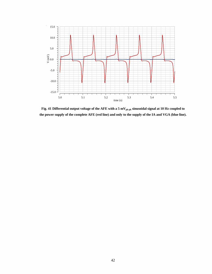
5.5 SMULATION WITH POWERLINE INTERFERENCE
Fig. 41 shows the transient power supply gain simulation result. The input signal
was a 5 mVpk-pk sinusoidal signal that was coupled to the 1.2 V DC power supply. The
red curve shows the differential output voltage of the AFE with the signal added to a
shared supply of the whole system (red curve), and blue curve shows the same output
when the interference signal was only added to a supply that is common to the IA and
VGA. Thus, it can be inferred that the LPNF limits the PSRR.
42
0.0
5.0
10.0
15.0
V (
mV
)
-15.0
-10.0
-5.0
5.55.0 5.1 5.2 5.3 5.4time (s)
Fig. 41 Differential output voltage of the AFE with a 5 mVpk-pk sinusoidal signal at 10 Hz coupled to
the power supply of the complete AFE (red line) and only to the supply of the IA and VGA (blue line).

43
6. PROTOTYPE CHIP AND PRINTED CIRCUIT BOARD DESIGN
6.1 FABRICATED CHIP
Fig. 42 displays a screenshot with the final chip layout of the complete
SCAFELAB project (analog front-end and digital calibration circuits) with bonding
pads. The chip was assembled in a PLCC84 package. Fig. 43 shows the complete
SCAFELAB die photo and the part with the analog front-end (zoomed-in).
Fig. 42 SCAFELAB chip layout.

44
IA
LPNF
VGA
Fig. 43 Chip micrograph of the fabricated EEG front-end with input impedance boosting capability
in IBM 0.13µm CMOS technology and zoomed-in analog front-end.

45
6.2 PCB DESIGN
For experimental verification, a printed circuit board (PCB) was designed and as-
sembled to provide off-chip bias voltages and currents, regulated supply voltages (for
individual blocks) and logic control bits. A differential driver IC (AD8131, with a gain
of 6 dB [37]) is employed on the board to generate a differential input signal from the
single-ended function generator (Agilent 33250A) and dynamic signal analyzer (HP
35665A). Two capacitors are connected between the output of the driver and the inputs
of the IA in order to block DC voltages at the differential driver outputs. Two BNC
connectors are placed at the differential output of the VGA. Fig. 44 displays a photo of
the SCLAFLAB PCB.
Single to differential driver Voltage regulator
AFE bias circuitry Calibration circuits bias
VGA gain control switch AFE differential outputIA gain control switch
Fig. 44 SCAFELAB PCB photo.

46
6.3 MEASUREMENT SETUP AND TEST DESCRIPTIONS
An Agilent E3646A power supply was used to provide the +/-5V supply voltages
for the differential driver (AD8131), instrumentation amplifier AD8421, and the +5V
voltage for the voltage regulator LM150 (that generates the 1.2V supply voltage for the
SCAFELAB chip). A B&K Precision 1672 power supply was employed to provide the
420 mV DC input for the noise and PSRR measurement. Sinusoidal inputs down to 2
mVpk-pk were generated with an Agilent 33250A arbitrary waveform generator. Several
10 dB (Mini-Circuits VAT-10W2+) and 20 dB attenuators (Mini-Circuits VAT-20W2+)
were used to reduce the input voltages to EEG signal levels. Depending on the test case,
a Tektronix DPO2024B oscilloscope or HP 35665A dynamic signal analyzer acquired
the output signals.
An instrumentation amplifier (AD8421 [38]) with an input impedance of 30 GΩ
was placed at the VGA output to convert the differential signal to a single-ended one as
well as to present a high impedance load that the VGA can drive. The AD8421 was on
an evaluation board (EVAL-INAMP-82RMZ [39]). This high-performance part was
selected to minimize impact on measurement results.

47
6.3.1 Gain Measurement
IA LPNF VGA
ATTENUATOR (S)
SCAFELAB PCB
DIFF
DRV
SCAFELAB CHIPAD8131
AD8421
IA
HP 35665A
Fig. 45 Systematic gain measurement setup.
Gain vs. frequency measurements were performed with an HP 35665A dynamic
signal analyzer using the setup in Fig. 45. The notch frequency of the low-pass notch
filter was manually tuned to 60 Hz by adjusting the bias current for its OTAs before
measuring the system gain. Since the dynamic signal analyzer only has a maximum of
800-line resolution in network analyzer mode, three different frequency ranges were
used to obtain the overall transfer function. According to [40], swept-sine analysis
(which has best accuracy) is only available at frequencies above 51.2 Hz with this
analyzer. A burst random source with an amplitude of 35 mVpeak was used to measure
the front-end transfer function with the lowest system gain mode. The amplitude was
then adjusted for the different gain modes. The uniform window option was utilized
during this measurement as suggested in the user manual. In the test setup, the attenua-
tors create a total input attenuation of 40 dB, and the single-ended to differential driver
has a gain of 6 dB, which both have to be de-embedded from the final gain measurement
results.

48
6.3.2 Nonlinearity Measurement
IA LPNF VGA
ATTENUATOR (S)
SCAFELAB PCB
DIFF
DRV
SCAFELAB CHIPAD8131
AD8421
IA
HP 35665A
Agilent 33250A
Fig. 46 Nonlinearity measurement setup.
To measure nonlinearity (second-order and third-order harmonic distortion), an
Agilent 33250A was used to generate a sinusoidal input at 5 Hz such that the third-order
harmonic distortion component is within the passband of the filter. According to [37],
the differential driver has an HD3 of at least 90 dBc at 5 Hz with small output voltage
swing, which is much higher than the simulated system specification. For the linearity
testing, a 40 dB attenuation was implemented with two attenuators because the minimum
output amplitude of the function generator (2 mVpk-pk) would be too high (outside of the
typical EEG signal range). The differential output of the AFE was combined with the
AD8421 and fed to the dynamic signal analyzer for fast Fourier transform (FFT) analysis
with the uniform window option. For the 4-16.5 Hz frequency range, the FFT was
obtained with 400-line resolution.

49
6.3.3 Noise Measurement
IA LPNF VGA
SCAFELAB PCBSCAFELAB CHIP
AD8421
IA
VDC=420mV
HP 35665A
Fig. 47 Noise measurement setup.
To measure the spectral noise density of the system, the inputs of the IA on the
chip were tied to a fixed DC voltage of 420 mV. Since the system gain is high, the front-
end output noise can be captured directly with the dynamic signal analyzer as visualized
in Fig. 47. Hence, the integrated input-referred noise can be calculated by dividing the
measured noise by the gain. Even though the noise bandwidth of the system is less than
50 Hz, the frequency range and line resolution of the HP 35665A were set the same as
during the gain measurement (0.5-200.5 Hz, 800 data point, uniform window) to ease the
calculation of the integrated input-referred noise after capturing the integrated input-
referred noise.

50
6.3.4 CMRR Measurement
verr
vcmDUT Gain = G
Fig. 48 CMRR test bench in general.
In published biosignal measurement systems, the CMRR and PSRR are usually re-
ported at a single frequency. To measure CMRR at a certain frequency, a common
practice is to apply a sinusoidal common-mode input signal (vcm) to the device under test
(DUT) and to measure the transient output amplitude as in the diagram of Fig. 48. The
measured output voltage amplitude is the common-mode error signal (verr), and the
common-mode gain is verr/vcm. Afterwards, the common-mode rejection ratio can be
calculated as
1020 err
cm
vCMRR log
G v
, (4)
where G is the differential gain of the DUT.
To better distinguish the error signal from noise, the FFT functionality of the dy-
namic signal analyzer was used to measure the common-mode output with the setup in
Fig. 49 instead of an oscilloscope. A 5 mVpk-pk sinusoidal input at 10 Hz was selected for
the CMRR measurement. Though the 5 mVpk-pk swing is much higher than the anticipat-
ed EEG signal level at the IA input, this test signal is just large enough so that the
common-mode output voltage appears above the noise floor. On the dynamic signal
analyzer, a 4-16.5 Hz frequency range and uniform window option were used for the
FFT analysis in this measurement with 400-line resolution.

51
IA LPNF VGA
SCAFELAB PCBSCAFELAB CHIP
AD8421
IA
Agilent 33250A
HP 35665A
Fig. 49 CMRR measurement setup.

52
6.3.5 PSRR Measurement
IA LPNF VGA
SCAFELAB PCBSCAFELAB CHIP
AD8421
IA
VDC=420mV
HP 35665A
Agilent 33250A
Fig. 50 PSRR measurement setup.
The PSRR measurement setup (Fig. 50) was similar to the CMRR measurement
described in the previous subsection, except that the sinusoidal input was superimposed
on the voltage supply instead of applied as common-mode input. The dynamic signal
analyzer was chosen instead of an oscilloscope for the same reason as during the CMRR
measurement. A 5 mVpk-pk sinusoidal input at 10 Hz was applied for the PSRR meas-
urement. This test signal was generated with an Agilent 33205A arbitrary waveform
generator together with a 1.255 V DC offset, which is the same voltage as the minimum
output of the low-dropout regulator (LDO) on the PCB that provided the DUT supply
voltage. The rest of the board was still powered by the on-board LDO so that the bias

53
voltages on the PCB are steady. On the dynamic signal analyzer, a 4-16.5 Hz frequency
range and uniform window option were used for the FFT analysis in this measurement
with 400-line resolution. The photo in Fig. 51 shows the complete measurement setup in
the laboratory.
Agilent E3648A
DC Power Supply
B&K Precision 1672
DC Power Supply
Agilent 32250A
Arbitrary Waveform
Generator
HP 35665A
Dynamic Signal Analyzer
SCAFELAB
PCB
AD8421
Eval Board
Fig. 51 Complete measurement setup on the bench.
6.4 MEASUREMENT RESULTS AND DISCUSSION
6.4.1 LPNF Tuning
As described in Section 3.6, the notch frequency of the LPNF has to be aligned to
60 Hz. Fig. 52 shows the frequency response of the analog front-end before LPNF
tuning. The two notch frequencies are 40 Hz and 60 Hz, which means one of the bias
current of the LPNF is was too small in the presence of fabrication process variations.
Fig. 53 shows the frequency response with the same gain setting after manual tuning of
the LPNF. Comparing the two plots, the tuned frequency response has more attenuation
near the notch frequency (> 67 dBc) at 59 Hz than the un-tuned response at 60 Hz (> 60
dBc). A residue of the 60 Hz powerline interference (~ 35.5 dBc) is still visible in the
tuned frequency response. The two transfer functions also show a 3 dB difference in the

54
passband gain, which is due to the change in the transconductance of the OTAs during
bias current tuning.
Fig. 52 Frequency response of the analog front-end before filter tuning.

55
Fig. 53 Frequency response of the analog front-end after filter tuning.
6.4.2 Gain Measurement Results
The IA in this AFE was designed to have three different gain settings, and the
VGA was designed to have seven gain settings. However, with process-voltage-
temperature variations, the maximum gain setting of the IA (50 dB) is not usable. Even
though the differential output of the IA (differential input of the LPNF) is not accessible
from outside of the chip, it can be assumed that the output offset of the IA (with highest
gain) saturates the LPNF stage. Hence, the system gain measurements were performed
with 30 dB and 40 dB gain settings in the IA, which implies a total number of 14 gain
settings for which the frequency responses are displayed in Fig. 54.

56
Fig. 54 AFE frequency responses for the 14 gain settings with 40 dB input attenuation and 6 dB driver gain of the test setup.

57
freq (Hz)100 101 102
Gain
(dB
)
20
30
40
50
60
70
80
90
100
Fig. 55 AFE frequency responses with IA in high gain mode and de-embedded test setup
gain/attenuation.
freq (Hz)100 101 102
Gain
(dB
)
-10
0
10
20
30
40
50
60
70
80
90
Fig. 56 AFE frequency responses with IA in low gain mode and de-embedded test setup
gain/attenuation.

58
Fig. 55 and Fig. 56 show the AFE transfer functions with IA in high and low gain
modes, where the -34 dB test bench gain (40 dB attenuation from the input attenuators, 6
dB gain from the differential driver) was de-embedded. The total AFE gain ranges from
66 dB to 93 dB with linear-in-dB steps. The results with higher gain modes are noisier
due to the smaller input amplitude used during the tests. The gain steps in the high IA
gain mode are less evenly distributed than those in the low IA gain mode, which is
mainly the result of the DC offset drift during the acquisition time. Fig. 55 and Fig. 56
demonstrate that the passband includes the complete target EEG frequency band from
0.5 to 40 Hz. As explained in Section 6.3.1, three different frequency ranges were used
to characterize the AFE transfer function. Fig. 57 displays the measured transfer function
with the lowest AFE gain setting, which was created by combining the data collected
from high-accuracy measurements spanning the three difference frequency ranges. The
plot reveals that the high-pass cut-off frequency due to the VGA stage is lower than 0.1
Hz.
Fig. 57 Frequency response with the lowest AFE gain setting over wide frequency range.
-30
-10
10
30
50
70
90
0.01 0.1 1 10 100 1000 10000
Gai
n (
dB
)
freq (Hz)

59
Fig. 58 and Fig. 59 show the transient output voltages with the maximum and min-
imum AFE gain modes. Since the system gain was overdesigned, the input signal
amplitude used for verification of the minimum gain mode is higher than the typical
EEG signal amplitude. The resulting large undistorted output voltage is clearly visible in
Fig. 58. Since the 5 Hz component is not clearly visible in the transient output in Fig. 59
with maximum gain (10 µVpk input signal amplitude), Fig. 60 shows the FFT from this
test case, which uncovers that the output signal is approximately 20 dB above the noise
floor.
Fig. 58 Measured transient output voltage of the AFE with 500 µVpk input at 5 Hz using the lowest
gain mode.

60
Fig. 59 Measured transient output voltage of the AFE with 10 µVpk input at 5 Hz using the maxi-
mum gain mode.
Fig. 60 FFT of the AFE output voltage with the same test condition as in Fig. 59.
6.4.3 Noise Measurement Result
Fig. 61 shows the output-referred noise of the complete AFE with the maximum
gain setting for the IA and minimum gain setting for the VGA. As expected, the flicker

61
noise dominates at the lower frequencies. Though the 60 Hz noise is strongly attenuated
by the notch in the filter, it is still visible in the output noise spectrum along with its
second-order and third-order harmonics at 120 Hz and 180 Hz.
Fig. 61 Output-referred noise measurement of the complete EEG front-end.
The integrated input-referred noise (IRN) was calculated after transfer of the raw
data to Matlab. The integrated IRN from 0.5 Hz to 45.5 Hz is 3.75 µVrms, which is high
compared with many reported state-of-the-art analog front-ends (Table 4). This is mainly
because the focus of the SCAFELAB project was on input impedance boosting but not
best-in-class noise performance. The impedance boosting methods was developed for a
widely used IA architecture, but is currently specific to the architecture. Best-in-class
front-end noise performance is typically achieved with particular IA design methods,
such as chopping techniques to minimize the impact of flicker noise, but the IA in the
presented front-end does not include noise enhancement features. Nevertheless, the
integrated noise of this front-end is still lower than that of some other designs (e.g., the
IA in [41] with a chopper-stabilized technique), and it is adequate for many EEG moni-

62
toring applications as demonstrated by the measurement results in this chapter. An
additional consideration is that the measurements were affected by test setup noise
sources, particularly when comparing the measured AFE noise with the simulated AFE
noise (integrated IRN from 0.5 Hz to 45.5 Hz: 2.16 µVrms) in Section 5.3.
6.4.4 Distortion Measurement
Fig. 62 shows that the third-order harmonic distortion (HD3) component is at least
51.3dB below the fundamental signal (51.3 dBc) with the maximum gain setting of the
IA and the minimum gain setting of the VGA (total gain: 75 dB) and a peak-to-peak
differential input voltage of 200 µV at 5Hz. This input amplitude and gain setting
combination was chosen to ensure that the input amplitude is within the typical EEG
signal range, while each stage has sufficient voltage headroom and the third-order
harmonic is not visible (i.e., below the noise floor). However, with the maximum IA
gain, the input DC offset of the LPNF stage can impair the overall linearity performance.
Note that the maximum IA gain was only chosen for this test to demonstrate the low-
distortion characteristic, but in normal mode of operation a low gain setting would be
used when the EEG signal strength is high. With higher (compared to the typical EEG
signal level) input amplitude of 600 µVpk-pk at the IA and the lowest front-end system
gain setting, the HD3 is at least 57dBc as shown in Fig. 63. From both figures, the
second-order harmonic is visible as expected from the simulation results that are ex-
plained in Section 5.2. The HD2 with low input signal level and higher gain is more
visible, which is likely to be caused by the larger output offset of the IA stage under this
test condition.

63
Fig. 62 Distortion measurement with a 200 µVpk-pk input at 5 Hz (with 75 dB gain).
Fig. 63 Distortion measurement with a 600 µVpk-pk input at 5 Hz (with 66 dB gain).

64
6.4.5 CMRR Measurement Result
Fig. 64 shows a 13.54 mVpk-pk differential output voltage of the AFE measured
with a sinusoidal common-mode input signal of 5 mVpk-pk at 10 Hz, resulting in a
common-mode gain of 8.65 dB. The differential AFE gain measured with the same gain
setting is 86.25 dB at 10 Hz. Thus, the common-mode rejection ratio (CMRR) is 77.6 dB.
Fig. 64 Differential output voltage of the AFE with a common-mode input sinusoidal signal of 5
mVpk-pk at 10 Hz.
6.4.6 PSRR Measurement Result
Fig. 65 displays the 6.15 mVpk-pk differential output voltage of the AFE that was
measured with a sinusoidal signal of 5 mVpk-pk at 10 Hz superimposed to the 1.255 V
power supply. The power supply gain in this case is 1.80 dB, and the measured differen-
tial gain at 10 Hz with this gain setting is 75.53 dB. Thus, the power supply rejection
ratio (PSRR) is 73.73 dB.

65
Fig. 65 Differential output voltage of the AFE with a sinusoidal input signal of 5 mVpk-pk at 10 Hz
coupled to the power supply voltage.
6.4.7 Measurement Summary
Table 4 lists the measurement results of the AFE in this work in comparison with
other state-of-the-art EEG AFEs reported in the literature. The supply voltage of this
work is 1.255 V, which is slightly higher than the standard 1.2 V supply for 0.13 µm
CMOS technology. The reason is that the voltage regulator (LM150) on the PCB can
only support an output voltage down to 1.255 V. The DC supply current of the system is
33.14 µA, excluding external bias circuitry. This total current is the sum of the supply
currents in the IA, LPNF and VGA stage. The LPNF is the only stage among the three
that does not have an independent voltage supply so that current of the LPNF could only
be estimated as 1.5x of the current from the simulation. The estimation factor 1.5x is
based on the other two stages, where the measured currents are both around 1.5x higher
than in the simulation results. The current of the AFE in this work is relatively high

66
compared with other reported AFEs. On one hand, the AFE in this work has more stages
than some of the other AFEs. Furthermore, the common-mode feedback circuits in this
work consume approximately 50% of the total current in both LPNF and VGA stage,
which are often not used in other works.
The AFE voltage gain ranges from 66 dB to 93 dB, which is a few decibels higher
than the simulated gain range. This is influenced by the mismatch of the resistors in the
IA stage and the capacitors in the VGA stage. The manual LPNF tuning also has an
effect on the gain, as explained in Section 6.4.1.
The CMRR and PSRR results are comparable with the state-of-the art. However,
the CMRR or PSRR can be further improved by applying better matching techniques for
the circuits in the differential signal path, both on the chip and on the board, or by
developing an on-chip LDO to improve the supply voltage quality.
The noise of this work is high due to the IA architecture. Chopping techniques are
applied in many recently reported EEG AFEs because the flicker noise is critical at low
frequencies. The test setup is also a contributor that adversely impacts the noise perfor-
mance, which is suggested by the fact that the measured noise is higher than the
simulated noise with foundry-supplied device models.
The total harmonic distortion (THD) for this work in Table 4 was calculated from
the measurement result shown in Fig. 63, which only includes the second-order and
third-order harmonics because the higher-order harmonics are below the noise floor.
In summary, the measurement results of this AFE are comparable with the state-
of-the-art in many aspects. Some specifications that are not as cutting edge as other
AFEs are predominantly limited by the instrumentation amplifier architecture. However,
the measured overall front-end performance is adequate.

67
Table 4 Comparison with state-of-the-art EEG analog front-ends
[41] [42] [43] [44] [45] [46] this work
Supply (V) 1 1.0 1.0 3 1.8 1.8 1.255
Current
consumption (µA) 1.8 3.5 0.337 3.6 58 0.9 33.14
*
Gain (dB) 40 40 45.6-60 72-81.6 42.9 40 66-93
CMRR (dB) 134 60 71 - 102 97 77.6***
PSRR (dB) 120 - 84 89 - - 74***
Noise RTI 6.7 µVrms
(0.5-100 Hz)
1.3 µVrms
(100 Hz)
2.5 µVrms(0.05-
460 Hz)
0.59 µVrms
(0.5-100 Hz)
0.65 µVrms
(0.5-100 Hz)
0.9 µVrms
(0.5-100 Hz) 3.75 µVrms
(0.5-45.5 Hz)
THD (%) - - 0.6 <1 - - 0.4
Technology 65 nm CMOS 0.18 µm CMOS 0.35 µm CMOS 0.35 µm CMOS 0.18 µm CMOS 0.18 µm CMOS 0.13 µm
CMOS
AFE Type**
CCIA IA TB-FEA+PGA
ACCIA+CSF
+VGA+GM
+Buffer
DAE DCCR-AFE IA+LPNF
+VGA
* LPNF current estimated as 1.5x of that in the simulation result; currents of other blocks were measured.
** IA = instrumentation amplifier, TB-FEA = tunable bandwidth front-end amplifier, PGA = programmable gain amplifier,
ACCIA = AC coupled chopper-stabilized instrumentation amplifier (ACCIA), CSF = chopping spike filter, VGA = variable gain
amplifier, GM = transconductance, DAE = digital active electrode, DCCR-AFE = dual-channel charge recycled analog front end,
CCIA = capacitively-coupled instrumentation amplifier.
*** Measured at 10 Hz.

68
7. CONCLUSION AND FUTURE WORK
Several design considerations for biosignal acquisition circuits were discussed in
this thesis. A fully-differential LPNF and a fully-differential VGA for EEG signal
measurements were proposed and designed. The presented circuits were combined with
an instrumentation amplifier to form a complete analog EEG front-end, which was
simulated, front-end achieves competitive performance measured and compared with
state-of-the-art designs reported in the literature. The specifications. It has a total power
consumption of 41.59 µW and a measured differential gain range from 66 to 93 dB. The
CMRR and PSRR of the complete front-end are 77.6 dB and 74 dB, respectively. The
measured input-referred noise is 3.75 µVrms integrated from 0.5 Hz to 45.5 Hz, and the
front-end has a THD of 0.4 %.
With regards to future work, the evolution of the proposed analog front-end with
input impedance boosting and fully-differential signal processing in the filter and
variable gain amplifier stages could include the combination of chopper-stabilized
design techniques to reduce the effects of DC offsets and flicker noise. Furthermore, to
achieve lower power consumption, it can be explored to devise a more efficient com-
mon-mode feedback circuit design methods. For the low-pass notch filter, an on-chip
digital calibration method can be developed to automatically tune the notch to the
frequency of the powerline interference. In the big picture, the EEG analog front-end in
the SCAFELAB project could become part of a wireless EEG signal acquisition system
with the combination of a low-power RF transceiver.

69
REFERENCES
[1] D. Pivonka, A. Yakovlev, A. Poon, and T. Meng, “A mm-sized wireless powered
and remotely controlled locomotive implant,” IEEE Trans. Biomedical Circuits
and Systems, vol. 6, no. 6, pp. 523-532, Jan. 2013.
[2] C. Becchetti and A. Neri, Medical Instrument Design and Development: From
Requirements to Market Placements, John Wiley & Sons, July 2013.
[3] S.-T. Kao, H. Lu, and C. Su, “A 1.5V 7.5µW programmable gain amplifier for
multiple biomedical signal acquisition,” in Proc. IEEE Biomedical Circuits and
Systems Conference (BioCAS), pp. 73-76, Nov. 2009.
[4] Y. Li, C. C. Y. Poon, and Y.-T. Zhang, “Analog integrated circuits design for
processing physiological signals,” IEEE Reviews in Biomedical Engineering, vol.
3, pp. 93-105, 2010.
[5] J. Silva-Martinez and J. Salcedo-Suñer, “IC voltage-to-current transducers with
very-small transconductance,” Analog Integrated Circuits and Signal Processing,
vol. 13, no. 3, pp. 285-293, 1997.
[6] A. Arnaud and C. Galup-Montoro “Pico-A/V range CMOS transconductors using
series-parallel current division", Electronics Letters, vol. 39, no. 18, pp.1295 -
1296, 2003.
[7] I. Olsson, R. H. D. Buhl, A. Sirota, G. Buzsaki, and K. Wise “Band-tunable and
multiplexed integrated circuits for simultaneous recording and stimulation with
microelectrode arrays,” IEEE Trans. Biomedical Engineering, vol. 52, no.
7, pp.1303 -1311, 2005.
[8] R. R. Harrison, "A low-power, low-noise CMOS amplifier for neural recording
applications", Proc. IEEE Int. Symp. Circuits and Systems, vol. 5, pp.197-200,
2002.
[9] E. C. M. Lim , X. D. Zou , Y. J Zheng, and J. Tan, “Design of low power low-
voltage biomedical amplifier for electrocardiogram signal recording,” Proc. IEEE
Biomedical Circuits Syst. Conf., pp.191 -194, 2007.
[10] Q. Fan, J. H. Huijsing, and K. A. A. Makinwa, “A 21nV/√Hz Chopper-Stabilized
Multi-Path Current-Feedback Instrumentation Amplifier With 2µV Offset,” IEEE
J. Solid-State Circuits, vol. 47, no. 2, pp. 464-475, Feb 2012.

70
[11] R. F. Yazicioglu, P. Merken, R. Puers, and C. Van Hoof, “A 60 µW 60 nV/√Hz
readout front-end for portable biopotential acquisition systems,” IEEE J. Solid-
State Circuits, vol. 42, no. 5, pp. 1100-1110, May 2007.
[12] A. Casson, D. Yates, S. Smith, J. Duncan, and E. Rodriguez-Villegas, “Wearable
electroencephalography,” IEEE Engineering in Medicine and Biology Magazine,
vol. 29, no. 3, pp. 44 - 56 , May-June 2010.
[13] Y. M. Chi, T.-P. Jung, and G. Cauwenberghs, “Dry-contact and noncontact
biopotential electrodes: methodological review,” IEEE Reviews in Biomedical En-
gineering, vol. 3, no. 1, pp. 106-119, Oct. 2010.
[14] C. Assambo and M. J. Burke, “Amplifier input impedance in dry electrode ECG
recording,” in Proc. Annual IEEE Conf. Engineering in Medicine and Biology So-
ciety (EMBC), pp. 1774-1777, Sept. 2009.
[15] C.-H. Chang and M. Onabajo, “Instrumentation amplifier input capacitance
cancellation for biopotential and bioimpedance measurements,” in Proc. IEEE Intl.
Midwest Symp. on Circuits and Systems (MWSCAS), pp. 539-542, Aug. 2014.
[16] K. Wang, C.-H. Chang, and M. Onabajo, “A fully-differential CMOS low-pass
notch filter for biosignal measurement devices with high interference rejection,”
in Proc. IEEE Intl. Midwest Symp. on Circuits and Systems (MWSCAS), pp. 1041-
1044, Aug. 2014.
[17] L. Xu, J. Feng, Y. Ni, and M. Onabajo, “Test signal generation for the calibration
of analog front-end circuits in biopotential measurement applications,” in Proc.
IEEE Intl. Midwest Symp. on Circuits and Systems (MWSCAS), pp. 949-952, Aug.
2014.
[18] L. Xu and M. Onabajo, “A low-power temperature-compensated relaxation
oscillator for built-in test signal generation,” in Proc. IEEE Intl. Midwest Symp. on
Circuits and Systems (MWSCAS), Aug. 2015.
[19] S. A. Zahrai and M. Onabajo, “A low-power hybrid ADC architecture for high-
speed medium-resolution applications,” in Proc. IEEE Intl. Midwest Symp. on Cir-
cuits and Systems (MWSCAS), Aug. 2015.

71
[20] C.-H. Chang and M. Onabajo, “Linearization of subthreshold low-noise amplifi-
ers,” in Proc. IEEE Intl. Symp. on Circuits and Systems (ISCAS), pp. 377-380,
May 2013.
[21] C.-H. Chang and M. Onabajo, “IIP3 enhancement of subthreshold active mix-
ers,” IEEE Trans. on Circuits and Systems II: Express Briefs, vol. 60, no. 11, pp.
731-735, Nov. 2013.
[22] L. Xu, K. Wang, C.-H. Chang, and M. Onabajo, “Inductorless linearization of low-
power active mixers,” in Proc. IEEE Intl. Symp. on Circuits and Systems (ISCAS),
pp. 2213-2216, May 2015.
[23] R. Schaumann, M. E. Van Valkenburg, Design of Analog Filters, New York,
Oxford, Oxford University Press, 2011.
[24] Texas Instruments. Active Filter Design Techniques. Available online:
http://www.ti.com/lit/ml/sloa088/sloa088.pdf
[25] Q. Huang and M. Oberle, “A 0.5-mW passive telemetry IC for biomedical applica-
tions,” IEEE J. Solid-State Circuits, vol. 33, pp. 937-946, 1998.
[26] X. Qian, Y. P. Xu, and X. Li, “A CMOS continuous-time low-pass notch filter for
EEG system,” Analog Integrated Circuits Signal Processing, vol. 44, no. 3, pp.
231-238, Sep. 2005.
[27] H. A. Alzaher, N. Tasadduq, and Y. Mahnashi, “A highly linear fully integrated
powerline filter for biopotential acquisition systems,” IEEE Trans. Biomedical
Circuits and Systems, vol. 7, no. 5, pp. 703-712, Oct. 2013.
[28] R. Martins, S. Selberherr, and F. A. Vaz, “A CMOS IC for portable EEG acquisi-
tion systems,” IEEE Trans. Instrumentation and Measurement, vol. 47, no. 5, pp.
1191-1196, Oct.1998.
[29] A. Worapishet, A. Demosthenous, and X. Liu, “A CMOS instrumentation amplifi-
er with 90-dB CMRR at 2-MHz using capacitive neutralization: analysis, design
considerations, and implementation,” IEEE Trans. Circuits and Systems I: Regular
Papers, vol. 58, no. 4, pp. 699-710, April 2011.
[30] A. Arnaud, R. Fiorelli, and C. Galup-Montoro, “Nanowatt, sub-nS OTAs, with
sub-10-mV input offset, using series-parallel current mirrors,” IEEE J. Solid-State
Circuits, vol. 41, no. 9, pp. 2009-2018, Sept. 2006.

72
[31] S. Solis-Bustos, J. Silva-Martinez, F. Maloberti, and E. Sanchez-Sinencio, “A 60
dB dynamic-range CMOS sixth-order 2.4 Hz low-pass filter for medical applica-
tions,” IEEE Trans. Circuits Syst. II, vol. 47, no. 12, pp. 1391-1398, Dec. 2000.
[32] J. Feng and M. Onabajo, “Wide dynamic range CMOS amplifier design for RF
signal power detection via electro-thermal coupling,” Springer J. Electronic Testing
(JETTA): Theory and Applications, vol. 30, no. 1, pp. 101-109, Feb. 2014.
[33] M. Onabajo and J. Silva-Martinez, “Mismatch reduction technique for transistors
with minimum channel length,” Analog Integrated Circuits and Signal Processing,
vol. 70, no. 3, pp. 429-435, March 2012.
[34] S. Sanei and J. A. Chambers, EEG Signal Processing. Chichester, U.K.: John
Wiley & Sons, Ltd., Sep. 2007.
[35] L. Hong, K. T. Tang, J. Y. Wu, G. Wang, “A digitally trimmable low noise low
power analog front end for EEG signal acquisition,” IEEE-EMBS Int. Conf. on Bi-
omedical and Health Informatics (BHI), pp. 208-211, Jan. 2012.
[36] M. Yin and M. Ghovanloo, “A low-noise preamplifier with adjustable gain and
bandwidth for biopotential recording applications,” IEEE Int. Symp. On Circuits
and Syst. (ISCAS), pp. 321-324, 2007.
[37] Analog Devices. Low-Cost, High Speed Differential Driver – AD8131. Online:
http://www.analog.com/media/en/technical-documentation/data-
sheets/AD8131.pdf
[38] Analog Devices. Precision Instrumentation Driver – AD8421. Online:
http://www.analog.com/media/en/technical-documentation/data-
sheets/AD8421.pdf
[39] Analog Devices. AD62X, AD822X, AD842X Series InAmp Evaluation Board.
Online: http://www.analog.com/media/en/technical-documentation/user-
guides/UG-261.pdf
[40] HP 35665A Dynamic Signal Analyzer Quick Start Guide. Available online:
http://exodus.poly.edu/~kurt/manuals/manuals/HP%20Agilent/HP%2035665A%2
0Quick%20Start%20Guide.pdf
[41] Q. Fan, F. Sebastiano, J. H. Huijsing, K. A. A. Makinwa, “A 1.8µW 60nV/√Hz
capacitively-coupled chopper instrumentation amplifier in 65nm CMOS for wire-

73
less sensor nodes,” IEEE J. Solid-State Circuits, vol. 47, no. 2, pp. 464-475, Feb
2012.
[42] N. Verma, A. Shoeb, J. Bohorquez, J. Dawson, J. Guttag, and A. P. Chandrakasan,
“A micro-power EEG acquisition SoC with integrated feature extraction processor
for a chronic seizure detection system,” IEEE J. Solid-State Circuits, vol. 45, no. 4,
pp. 804–816, Apr. 2010.
[43] X. Zou, W. Liew, L. Yao, and L. Yong, “A 1-V 450-nW fully integrated pro-
grammable biomedical sensor interface chip,” IEEE J. Solid-State Circuits, vol. 44,
pp. 1067–1077, Apr. 2009.
[44] R. F. Yazicioglu, P. Merken, R. Puers, and C. V. Hoof, “A 200 µW eight channel
EEG acquisition ASIC for ambulatory EEG systems,” IEEE J. Solid-State Circuits,
vol. 43, no. 12, pp. 3025-3038, Dec. 2008.
[45] J. Xu, B. Busze, C. V. Hoof, K. A. A. Makinwa, and R. F. Yazicioglu, “A 15-
channel digital active electrode system for multi-parameter biopotential measure-
ment,” IEEE J. Solid-State Circuits, vol. 50, no. 9, pp. 2090-2100, Sep. 2015.
[46] Muhammad Awais Bin Altaf, Chen Zhang and Jerald Yoo, “A 16-channel patient-
specific seizure onset and termination detection SoC with impedance-adaptive
transcranial electrical stimulator,” IEEE J. Solid-State Circuits, vol. 50, no. 11, pp.
2728-2740, Nov. 2015.

74
APPENDIX
Table 5 Device parameters of the OTA in the LPNF stage (Fig. 13)
Device Dimensions [width (µm)/length (µm)] Multiplier
M1-M16 0.6/5 2
M17-M22 0.5/5 2
M23, M24 0.3/5 80
M25-M30 0.3/5 2
Table 6 Device parameters of the CMFB amplifier in the LPNF stage (Fig. 14)
Device Dimensions [width (µm)/length (µm)] Multiplier
M31-M34 0.5/5 2
M35 1/5 20
M36, M37 1/5 10
Table 7 Device parameters of the OTA in the VGA stage (Fig. 27)
Device Dimensions [width (µm)/length (µm)] Multiplier
M1, M2 5/3 8
M3, M4 0.5/3 8
M5, M6 0.5/3 2
M7-M10 0.6/5 2

75
Table 8 Device parameters of the pseudo-resistor in the VGA stage (Fig. 28)
Device Dimensions [width (µm)/length (µm)] Multiplier
M11-M26 0.5/5 1
Table 9 Device parameters of the CMFB amplifier in the VGA stage
Device Dimensions [width (µm)/length (µm)] Multiplier
M27-M30 5/3 8
M31 5/3 8
M32, M33 5/3 4
M27 M28 M29 M30
M31M32 M33
vCMFB
VCM
vin_CMFBvip_CMFB
Ibias3 Ibias4
Fig. 66 Schematic of the CMFB amplifier in the VGA stage.