high-performance delta-sigma analog-to-digital …moon/research/files/jose_silva.pdfhigh-performance...
TRANSCRIPT
High-Performance Delta-Sigma Analog-to-Digital Converters
by
Jose Barreiro da Silva
A THESIS
submitted to
Oregon State University
in partial fulfillment ofthe requirements for the
degree of
Doctor of Philosophy
Presented July 14, 2004Commencement June 2005

ACKNOWLEDGMENTS
I wish to express my deepest gratitude to my research advisors, Dr. Gabor Temes
and Dr. Un-Ku Moon, who provided me with an excellent research environment. I feel
greatly honored to have worked under the guidance of Dr. Temes. I benefited from
his extensive knowledge in circuit design, invaluable teaching and research skills, and
support in technical and personal matters. I thank him for his kindness, friendship,
and for being a source of inspiration at every level. It was also a great honor to have
been advised by Dr. Moon. I learned many fundamental circuit design skills from him.
I appreciated his enthusiastic, always honest feedback. I thank him for his valuable
guidance and encouragement throughout my research.
I would like to thank Prof. Karti Mayaram, Prof. Huaping Liu, Dr. Adrian Early
and Prof. Bruce D’Ambrosio for serving in my graduate committee.
I am grateful to my close friends Matt Brown, Pavan Hanumolu, Jose Ceballos
and Gilcho Ahn, for many fruitful and good-humored discussions, for their help with
technical and non-technical matters, and for countless pleasant memories from our time
together. In particular, I thank Pavan for helping me to keep things in perspective, and
Jose Ceballos for his delightful cheerfulness. I have a special appreciation for Matt, for
his genuine concern for my personal well-being, and for his kind help during difficult
times.
I also wish to acknowledge all my officemates, who contributed in many ways
to an outstanding environment: in no particular order, I would like to acknowledge
Xuesheng Wang, Mingyu Kim, Merrick Brownlee, Vova, Charlie Myers, Kerem Ok,
Shelly Xiao, Anurag Pulincherry, Jipeng Li, Mustafa Keskin, Dong-Young Chang, Kye-
Hyung Lee, Younjae Kook, Byung-Moo Min, Ranganathan Desikachari, Kiseok Yoo,
Zhenyong Zhang, Ting Wu, Dan Thomas, Brandon Greenley and Jacob Zechmann.
I was fortunate to spend my first years at OSU with Tetsuya Kajita, with whom
I shared many classes and group projects. I’m grateful for the wonderful times that we

spent together and with his family. I have high esteem for Janos Markus and Johanna
Markus for many memorable experiences shared together. I wish to thank Mutsuko
Kajita, Melinda Valencia and Marcela Andolina, for their help, friendship and for many
enjoyable moments outside the research environment. I am grateful to Ibi Temes for her
kindness, and for many delightful visits to the Temes’ home.
My teaching assistantships at OSU were significant in the development of my
knowledge of circuits and systems. For that, I wish to acknowledge all the students who
helped by asking hard questions.
For their important contributions to this work, I wish to thank Dr. Xuesheng
Wang, Robert Batten, Dr. Peter Kiss, Dr. Jesper Steensgaard and Dr. Anas Hamoui. I
am indebted to Paul Ferguson, Richard Schreier, Steve Lewis, and many other people at
Analog Devices, for their help with design reviews, and for their invaluable feedback on
many circuit design and testing issues. I’m thankful to Jonathan Schweitzer of Lucent
Technologies for fabricating the first prototype. I would also like to thank Bill McIntyre,
Keith Schoendoerfer, Arun Rao and Mengzhe Ma, at National Semiconductor Corpo-
ration, for their help with the fabrication of the second prototype chips. I appreciate
George Corrigan, Terry McMahon and Keith Moore, at Hewlett Packard, for their as-
sistance with FIB modifications. This work would not have been possible without the
generous financial support provided by the NSF Center for the Design of Analog and
Digital Integrated Circuits (CDADIC).
I wish to thank the ECE office staff for their top-quality support, and for always
letting me know when there were cookies in the office: Sarah O’Leary, Ferne Simendinger,
Morgan Garrison, Clara Knutson, Brian Lindsey, Nancy Brown, Cory Williams and Tina
Batten. I’m also grateful to Chris Tasker and Manfred Dittrich for their help with my
test setup preparations.
Finally, words cannot adequately express my deepest gratitude to my sister and to
my deceased parents, who demonstrated in so many admirable ways their unconditional
love and support throughout my life.
TABLE OF CONTENTS
Page
1. INTRODUCTION . . . . . . . . . . . . . . . . . . . . . . . . . . . . . . . . . . . . . . . . . . . . . . . . . . . . . . . . . 1
1.1. Motivation . . . . . . . . . . . . . . . . . . . . . . . . . . . . . . . . . . . . . . . . . . . . . . . . . . . . . . . . . . . . 1
1.2. Contributions . . . . . . . . . . . . . . . . . . . . . . . . . . . . . . . . . . . . . . . . . . . . . . . . . . . . . . . . . 3
1.3. Thesis Organization . . . . . . . . . . . . . . . . . . . . . . . . . . . . . . . . . . . . . . . . . . . . . . . . . . . 4
2. DELTA-SIGMA BASICS . . . . . . . . . . . . . . . . . . . . . . . . . . . . . . . . . . . . . . . . . . . . . . . . . . . 6
2.1. Nyquist-Rate vs Oversampling Converters . . . . . . . . . . . . . . . . . . . . . . . . . . . . . 6
2.2. Data Converter Performance Metrics . . . . . . . . . . . . . . . . . . . . . . . . . . . . . . . . . . 9
2.3. Quantization Noise Analysis. . . . . . . . . . . . . . . . . . . . . . . . . . . . . . . . . . . . . . . . . . . 10
2.4. Oversampling . . . . . . . . . . . . . . . . . . . . . . . . . . . . . . . . . . . . . . . . . . . . . . . . . . . . . . . . . 13
2.5. First-Order Noise Shaping. . . . . . . . . . . . . . . . . . . . . . . . . . . . . . . . . . . . . . . . . . . . . 15
2.5.1. Circuit Implementation . . . . . . . . . . . . . . . . . . . . . . . . . . . . . . . . . . . . . . . . 182.5.2. Simulations . . . . . . . . . . . . . . . . . . . . . . . . . . . . . . . . . . . . . . . . . . . . . . . . . . . . 20
2.6. Second-Order Noise Shaping . . . . . . . . . . . . . . . . . . . . . . . . . . . . . . . . . . . . . . . . . . 20
2.7. Generalization . . . . . . . . . . . . . . . . . . . . . . . . . . . . . . . . . . . . . . . . . . . . . . . . . . . . . . . . 22
2.8. Nonideal Effects. . . . . . . . . . . . . . . . . . . . . . . . . . . . . . . . . . . . . . . . . . . . . . . . . . . . . . . 24
2.8.1. Tones and Limit Cycles . . . . . . . . . . . . . . . . . . . . . . . . . . . . . . . . . . . . . . . . 252.8.2. Finite Opamp Gain and Coefficient Errors. . . . . . . . . . . . . . . . . . . . . . 262.8.3. Stability . . . . . . . . . . . . . . . . . . . . . . . . . . . . . . . . . . . . . . . . . . . . . . . . . . . . . . . 27
2.9. Multi-Stage Noise Shaping . . . . . . . . . . . . . . . . . . . . . . . . . . . . . . . . . . . . . . . . . . . . 29
2.9.1. Theory of Operation . . . . . . . . . . . . . . . . . . . . . . . . . . . . . . . . . . . . . . . . . . . 30
2.10. Advanced Topics . . . . . . . . . . . . . . . . . . . . . . . . . . . . . . . . . . . . . . . . . . . . . . . . . . . . . . 32
3. PROBLEMS IN WIDEBAND MASH ADCS . . . . . . . . . . . . . . . . . . . . . . . . . . . . . . . 34
3.1. Distortion . . . . . . . . . . . . . . . . . . . . . . . . . . . . . . . . . . . . . . . . . . . . . . . . . . . . . . . . . . . . . 34
3.2. Matching of Analog and Digital NTFs. . . . . . . . . . . . . . . . . . . . . . . . . . . . . . . . . 36
3.3. Nonlinearities in multibit DACs . . . . . . . . . . . . . . . . . . . . . . . . . . . . . . . . . . . . . . . 38
TABLE OF CONTENTS (Continued)
Page
3.4. Traditional Solutions (State of the Art) . . . . . . . . . . . . . . . . . . . . . . . . . . . . . . . 42
4. PROPOSED SOLUTIONS . . . . . . . . . . . . . . . . . . . . . . . . . . . . . . . . . . . . . . . . . . . . . . . . . 45
4.1. Low-Distortion Delta-Sigma Topologies. . . . . . . . . . . . . . . . . . . . . . . . . . . . . . . . 45
4.1.1. Lower Area and Power Consumption in Multibit Implementations 474.1.2. Improved Input Signal Range . . . . . . . . . . . . . . . . . . . . . . . . . . . . . . . . . . 494.1.3. Only one DAC Needed in the Feedback Path . . . . . . . . . . . . . . . . . . . 494.1.4. Simplified MASH Architecture . . . . . . . . . . . . . . . . . . . . . . . . . . . . . . . . . 49
4.2. Adaptive Compensation of Analog Imperfections . . . . . . . . . . . . . . . . . . . . . . 50
4.2.1. Adaptive Noise Cancellation Basics . . . . . . . . . . . . . . . . . . . . . . . . . . . . 524.2.2. Adaptive Compensation of Quantization Noise Leakage . . . . . . . . . 534.2.3. Adaptive Algorithms . . . . . . . . . . . . . . . . . . . . . . . . . . . . . . . . . . . . . . . . . . . 544.2.4. Quantization Noise Leakage Compensation in Low-Distortion
∆Σ Topologies . . . . . . . . . . . . . . . . . . . . . . . . . . . . . . . . . . . . . . . . . . . . . . . . . 56
4.3. Digital Estimation and Correction of DAC Errors . . . . . . . . . . . . . . . . . . . . . 58
5. A HIGH-PERFORMANCE DELTA-SIGMA ADC . . . . . . . . . . . . . . . . . . . . . . . . . . 63
5.1. MASH 2-2-2 Architecture . . . . . . . . . . . . . . . . . . . . . . . . . . . . . . . . . . . . . . . . . . . . . 63
5.1.1. Theoretical Performance . . . . . . . . . . . . . . . . . . . . . . . . . . . . . . . . . . . . . . . 65
5.2. System-Level Simplifications . . . . . . . . . . . . . . . . . . . . . . . . . . . . . . . . . . . . . . . . . . 66
5.2.1. Adaptive Filter Coefficients . . . . . . . . . . . . . . . . . . . . . . . . . . . . . . . . . . . . 685.2.2. System Level Simulations . . . . . . . . . . . . . . . . . . . . . . . . . . . . . . . . . . . . . . 69
6. NOISE AND LINEARITY REQUIREMENTS . . . . . . . . . . . . . . . . . . . . . . . . . . . . . 72
6.1. Noise Analysis . . . . . . . . . . . . . . . . . . . . . . . . . . . . . . . . . . . . . . . . . . . . . . . . . . . . . . . . 72
6.2. Noise Sources . . . . . . . . . . . . . . . . . . . . . . . . . . . . . . . . . . . . . . . . . . . . . . . . . . . . . . . . . 73
6.2.1. kT/C Noise . . . . . . . . . . . . . . . . . . . . . . . . . . . . . . . . . . . . . . . . . . . . . . . . . . . . 746.2.2. Opamp Noise . . . . . . . . . . . . . . . . . . . . . . . . . . . . . . . . . . . . . . . . . . . . . . . . . . 75

TABLE OF CONTENTS (Continued)
Page
6.3. Effect of Thermal Noise on the MASH ADC Performance . . . . . . . . . . . . . 77
6.3.1. Capacitor Sizing . . . . . . . . . . . . . . . . . . . . . . . . . . . . . . . . . . . . . . . . . . . . . . . 78
6.4. Quantizer Linearity . . . . . . . . . . . . . . . . . . . . . . . . . . . . . . . . . . . . . . . . . . . . . . . . . . . 79
6.5. DAC Linearity . . . . . . . . . . . . . . . . . . . . . . . . . . . . . . . . . . . . . . . . . . . . . . . . . . . . . . . . 81
6.6. Digital Truncation Noise . . . . . . . . . . . . . . . . . . . . . . . . . . . . . . . . . . . . . . . . . . . . . . 82
6.7. Noise Summary . . . . . . . . . . . . . . . . . . . . . . . . . . . . . . . . . . . . . . . . . . . . . . . . . . . . . . . 82
7. PROTOTYPE CHIP DESIGN — ANALOG SECTION . . . . . . . . . . . . . . . . . . . . 84
7.1. Modulator Stages . . . . . . . . . . . . . . . . . . . . . . . . . . . . . . . . . . . . . . . . . . . . . . . . . . . . . 84
7.2. Switch Design . . . . . . . . . . . . . . . . . . . . . . . . . . . . . . . . . . . . . . . . . . . . . . . . . . . . . . . . . 85
7.2.1. Switch Types and Sizes . . . . . . . . . . . . . . . . . . . . . . . . . . . . . . . . . . . . . . . . 857.2.2. Bootstrapped Switches . . . . . . . . . . . . . . . . . . . . . . . . . . . . . . . . . . . . . . . . . 89
7.3. Opamp Design . . . . . . . . . . . . . . . . . . . . . . . . . . . . . . . . . . . . . . . . . . . . . . . . . . . . . . . . 91
7.3.1. Opamp Requirements . . . . . . . . . . . . . . . . . . . . . . . . . . . . . . . . . . . . . . . . . . 927.3.2. Loop-Gain Specifications . . . . . . . . . . . . . . . . . . . . . . . . . . . . . . . . . . . . . . . 957.3.3. Opamp Problems . . . . . . . . . . . . . . . . . . . . . . . . . . . . . . . . . . . . . . . . . . . . . . 96
7.4. Quantizers . . . . . . . . . . . . . . . . . . . . . . . . . . . . . . . . . . . . . . . . . . . . . . . . . . . . . . . . . . . . 98
7.4.1. Effects of Passive Adder on Quantizer . . . . . . . . . . . . . . . . . . . . . . . . . . 997.4.2. Comparator Design . . . . . . . . . . . . . . . . . . . . . . . . . . . . . . . . . . . . . . . . . . . . 101
8. PROTOTYPE CHIP DESIGN — DIGITAL SECTION . . . . . . . . . . . . . . . . . . . . 105
8.1. Encoders . . . . . . . . . . . . . . . . . . . . . . . . . . . . . . . . . . . . . . . . . . . . . . . . . . . . . . . . . . . . . . 105
8.2. Scrambler . . . . . . . . . . . . . . . . . . . . . . . . . . . . . . . . . . . . . . . . . . . . . . . . . . . . . . . . . . . . . 107
8.2.1. Scrambler Delay . . . . . . . . . . . . . . . . . . . . . . . . . . . . . . . . . . . . . . . . . . . . . . . 108
8.3. Noise Cancellation Logic . . . . . . . . . . . . . . . . . . . . . . . . . . . . . . . . . . . . . . . . . . . . . . 110
8.3.1. FIR and Correlation Blocks . . . . . . . . . . . . . . . . . . . . . . . . . . . . . . . . . . . . 1108.3.2. FIR Coefficients . . . . . . . . . . . . . . . . . . . . . . . . . . . . . . . . . . . . . . . . . . . . . . . 1138.3.3. Multipliers . . . . . . . . . . . . . . . . . . . . . . . . . . . . . . . . . . . . . . . . . . . . . . . . . . . . . 114
TABLE OF CONTENTS (Continued)
Page
8.3.4. Correlators . . . . . . . . . . . . . . . . . . . . . . . . . . . . . . . . . . . . . . . . . . . . . . . . . . . . 1158.3.5. Synchronization . . . . . . . . . . . . . . . . . . . . . . . . . . . . . . . . . . . . . . . . . . . . . . . . 115
8.4. Additions/Scaling . . . . . . . . . . . . . . . . . . . . . . . . . . . . . . . . . . . . . . . . . . . . . . . . . . . . . 116
8.5. Clock generator . . . . . . . . . . . . . . . . . . . . . . . . . . . . . . . . . . . . . . . . . . . . . . . . . . . . . . . 117
8.6. Minimizing Crosstalk Noise Between the Analog and Digital Section . . . 118
8.7. Output Interface and Test Modes . . . . . . . . . . . . . . . . . . . . . . . . . . . . . . . . . . . . . 119
8.8. Layout Considerations . . . . . . . . . . . . . . . . . . . . . . . . . . . . . . . . . . . . . . . . . . . . . . . . 121
9. TEST SETUP AND EXPERIMENTAL RESULTS . . . . . . . . . . . . . . . . . . . . . . . . . 123
9.1. Test Board Design . . . . . . . . . . . . . . . . . . . . . . . . . . . . . . . . . . . . . . . . . . . . . . . . . . . . 123
9.2. Experimental Results . . . . . . . . . . . . . . . . . . . . . . . . . . . . . . . . . . . . . . . . . . . . . . . . . 125
9.2.1. Design Corrections . . . . . . . . . . . . . . . . . . . . . . . . . . . . . . . . . . . . . . . . . . . . . 1269.2.2. DAC error estimation and correction . . . . . . . . . . . . . . . . . . . . . . . . . . . 1279.2.3. Performance Measurements . . . . . . . . . . . . . . . . . . . . . . . . . . . . . . . . . . . . 1289.2.4. Power Consumption . . . . . . . . . . . . . . . . . . . . . . . . . . . . . . . . . . . . . . . . . . . 131
10. CONCLUSIONS . . . . . . . . . . . . . . . . . . . . . . . . . . . . . . . . . . . . . . . . . . . . . . . . . . . . . . . . . . 132
10.1. Conclusions . . . . . . . . . . . . . . . . . . . . . . . . . . . . . . . . . . . . . . . . . . . . . . . . . . . . . . . . . . . 132
10.2. Future Work . . . . . . . . . . . . . . . . . . . . . . . . . . . . . . . . . . . . . . . . . . . . . . . . . . . . . . . . . . 133
BIBLIOGRAPHY . . . . . . . . . . . . . . . . . . . . . . . . . . . . . . . . . . . . . . . . . . . . . . . . . . . . . . . . . . . . . . 134
LIST OF FIGURES
Figure Page
1.1 Types of analog-to-digital converters . . . . . . . . . . . . . . . . . . . . . . . . . . . . . . . . . . . 2
2.1 Block diagram of a Nyquist-rate ADC . . . . . . . . . . . . . . . . . . . . . . . . . . . . . . . . . 7
2.2 Block diagram of an oversampling ADC. . . . . . . . . . . . . . . . . . . . . . . . . . . . . . . . 7
2.3 Block diagram of a Nyquist-rate DAC . . . . . . . . . . . . . . . . . . . . . . . . . . . . . . . . . 8
2.4 Block diagram of an oversampling DAC . . . . . . . . . . . . . . . . . . . . . . . . . . . . . . . . 9
2.5 Generic ADC and its quantization error . . . . . . . . . . . . . . . . . . . . . . . . . . . . . . . . 11
2.6 Quantizer DC transfer curve and quantization error . . . . . . . . . . . . . . . . . . . . 11
2.7 Probability density function and power spectral density of quantizationnoise . . . . . . . . . . . . . . . . . . . . . . . . . . . . . . . . . . . . . . . . . . . . . . . . . . . . . . . . . . . . . . . . . . 12
2.8 Oversampling . . . . . . . . . . . . . . . . . . . . . . . . . . . . . . . . . . . . . . . . . . . . . . . . . . . . . . . . . 14
2.9 First-order ∆Σ modulator . . . . . . . . . . . . . . . . . . . . . . . . . . . . . . . . . . . . . . . . . . . . . 15
2.10 Noise transfer function of a first-order delta-sigma modulator . . . . . . . . . . . 17
2.11 Output spectrum of a first-order delta-sigma modulator . . . . . . . . . . . . . . . . 18
2.12 Circuit implementation of a first-order A/D delta-sigma modulator . . . . . 18
2.13 Circuit implementation of a first-order D/A ∆Σ modulator . . . . . . . . . . . . . 19
2.14 Simulations of a first-order ∆Σ modulator . . . . . . . . . . . . . . . . . . . . . . . . . . . . . 21
2.15 Second-order ∆Σ modulator . . . . . . . . . . . . . . . . . . . . . . . . . . . . . . . . . . . . . . . . . . . 21
2.16 Output spectrum of a second-order delta-sigma modulator . . . . . . . . . . . . . 22
2.17 SQNR improvement for general noise shaping . . . . . . . . . . . . . . . . . . . . . . . . . . 23
2.18 Effect of limit cycles on the in-band noise power . . . . . . . . . . . . . . . . . . . . . . . 25
2.19 Using dither to prevent tones and limit cycles . . . . . . . . . . . . . . . . . . . . . . . . . . 26
2.20 Effect of finite opamp gain on NTF . . . . . . . . . . . . . . . . . . . . . . . . . . . . . . . . . . . . 27
2.21 Quantizer gain . . . . . . . . . . . . . . . . . . . . . . . . . . . . . . . . . . . . . . . . . . . . . . . . . . . . . . . . 27
LIST OF FIGURES (Continued)
Figure Page
2.22 Stability . . . . . . . . . . . . . . . . . . . . . . . . . . . . . . . . . . . . . . . . . . . . . . . . . . . . . . . . . . . . . . . 28
2.23 Illustration of Lee’s rule . . . . . . . . . . . . . . . . . . . . . . . . . . . . . . . . . . . . . . . . . . . . . . . 29
2.24 MASH diagram. . . . . . . . . . . . . . . . . . . . . . . . . . . . . . . . . . . . . . . . . . . . . . . . . . . . . . . . 30
2.25 MASH 2-0 diagram . . . . . . . . . . . . . . . . . . . . . . . . . . . . . . . . . . . . . . . . . . . . . . . . . . . . 31
3.1 Distortion in ∆Σ modulators . . . . . . . . . . . . . . . . . . . . . . . . . . . . . . . . . . . . . . . . . . 34
3.2 Transfer functions from the integrator outputs to the modulator output 35
3.3 Simulation for nonlinear opamp gain . . . . . . . . . . . . . . . . . . . . . . . . . . . . . . . . . . . 36
3.4 MASH 2-0 diagram . . . . . . . . . . . . . . . . . . . . . . . . . . . . . . . . . . . . . . . . . . . . . . . . . . . . 37
3.5 Effect of mismatches between the analog and digital noise transfer func-tions . . . . . . . . . . . . . . . . . . . . . . . . . . . . . . . . . . . . . . . . . . . . . . . . . . . . . . . . . . . . . . . . . . 37
3.6 DAC linearity . . . . . . . . . . . . . . . . . . . . . . . . . . . . . . . . . . . . . . . . . . . . . . . . . . . . . . . . . 39
3.7 Effect of DAC nonlinearities on ADC performance . . . . . . . . . . . . . . . . . . . . . 40
3.8 Example of unit-element selection for the DWA algorithm . . . . . . . . . . . . . . 41
4.1 Low-distortion topology . . . . . . . . . . . . . . . . . . . . . . . . . . . . . . . . . . . . . . . . . . . . . . . 45
4.2 Comparison between traditional and low-distortion topologies . . . . . . . . . . 47
4.3 Tapping the quantization error for a low-distortion topology . . . . . . . . . . . . 50
4.4 MASH 2-0 diagram with analog coefficients . . . . . . . . . . . . . . . . . . . . . . . . . . . . 51
4.5 Adaptive filter basics . . . . . . . . . . . . . . . . . . . . . . . . . . . . . . . . . . . . . . . . . . . . . . . . . . 52
4.6 Adaptive noise cancellation used in the MASH 2-0 structure. . . . . . . . . . . . 54
4.7 Simulations for MASH 2-0 structure, before and after correction . . . . . . . . 56
4.8 MASH 2-0 with low-distortion topology . . . . . . . . . . . . . . . . . . . . . . . . . . . . . . . . 57
4.9 Unit-element DAC model . . . . . . . . . . . . . . . . . . . . . . . . . . . . . . . . . . . . . . . . . . . . . . 59
4.10 Estimation of DAC errors. . . . . . . . . . . . . . . . . . . . . . . . . . . . . . . . . . . . . . . . . . . . . . 60

LIST OF FIGURES (Continued)
Figure Page
4.11 Correction of DAC errors . . . . . . . . . . . . . . . . . . . . . . . . . . . . . . . . . . . . . . . . . . . . . . 61
4.12 Estimation and correction of DAC errors in a delta-sigma loop . . . . . . . . . 62
5.1 MASH 2-2-2 with correction . . . . . . . . . . . . . . . . . . . . . . . . . . . . . . . . . . . . . . . . . . . 65
5.2 MASH ADC prototype . . . . . . . . . . . . . . . . . . . . . . . . . . . . . . . . . . . . . . . . . . . . . . . . 66
5.3 First-stage diagram . . . . . . . . . . . . . . . . . . . . . . . . . . . . . . . . . . . . . . . . . . . . . . . . . . . . 67
5.4 Diagram for the second and third stages . . . . . . . . . . . . . . . . . . . . . . . . . . . . . . . 67
5.5 System level simulations . . . . . . . . . . . . . . . . . . . . . . . . . . . . . . . . . . . . . . . . . . . . . . . 70
5.6 SNDR versus input signal amplitude . . . . . . . . . . . . . . . . . . . . . . . . . . . . . . . . . . . 71
6.1 Noise sources in a low-distortion modulator . . . . . . . . . . . . . . . . . . . . . . . . . . . . 74
6.2 Equivalent representation of the noise sources . . . . . . . . . . . . . . . . . . . . . . . . . . 74
6.3 Opamp noise spectrum . . . . . . . . . . . . . . . . . . . . . . . . . . . . . . . . . . . . . . . . . . . . . . . . 76
6.4 Noise gains from each sampling capacitor to the MASH ADC output . . . 77
6.5 Relation between Cs11 and Cs12 for the targeted noise . . . . . . . . . . . . . . . . . 80
6.6 Transfer functions for DAC nonlinearities . . . . . . . . . . . . . . . . . . . . . . . . . . . . . . 82
7.1 First stage diagram . . . . . . . . . . . . . . . . . . . . . . . . . . . . . . . . . . . . . . . . . . . . . . . . . . . . 85
7.2 Fully-differential schematic of the first-stage modulator . . . . . . . . . . . . . . . . . 86
7.3 Second- and third-stage diagram . . . . . . . . . . . . . . . . . . . . . . . . . . . . . . . . . . . . . . . 87
7.4 Settling . . . . . . . . . . . . . . . . . . . . . . . . . . . . . . . . . . . . . . . . . . . . . . . . . . . . . . . . . . . . . . . 87
7.5 Switch configurations . . . . . . . . . . . . . . . . . . . . . . . . . . . . . . . . . . . . . . . . . . . . . . . . . . 89
7.6 Critical switches in the first stage . . . . . . . . . . . . . . . . . . . . . . . . . . . . . . . . . . . . . . 90
7.7 Diagram of the bootstrapping switch. . . . . . . . . . . . . . . . . . . . . . . . . . . . . . . . . . . 90
7.8 Schematic of the bootstrap switch . . . . . . . . . . . . . . . . . . . . . . . . . . . . . . . . . . . . . 91
7.9 Distortion of the bootstrap switch . . . . . . . . . . . . . . . . . . . . . . . . . . . . . . . . . . . . . 91

LIST OF FIGURES (Continued)
Figure Page
7.10 Opamp configurations . . . . . . . . . . . . . . . . . . . . . . . . . . . . . . . . . . . . . . . . . . . . . . . . . 92
7.11 Opamp schematic . . . . . . . . . . . . . . . . . . . . . . . . . . . . . . . . . . . . . . . . . . . . . . . . . . . . . 94
7.12 Opamp problem . . . . . . . . . . . . . . . . . . . . . . . . . . . . . . . . . . . . . . . . . . . . . . . . . . . . . . . 97
7.13 Improving the settling behavior of opamp 22 . . . . . . . . . . . . . . . . . . . . . . . . . . . 98
7.14 Quantizer diagram . . . . . . . . . . . . . . . . . . . . . . . . . . . . . . . . . . . . . . . . . . . . . . . . . . . . 100
7.15 Passive switched-capacitor adder during Φ1 . . . . . . . . . . . . . . . . . . . . . . . . . . . . 101
7.16 Comparator diagram . . . . . . . . . . . . . . . . . . . . . . . . . . . . . . . . . . . . . . . . . . . . . . . . . . 102
7.17 Comparator schematic . . . . . . . . . . . . . . . . . . . . . . . . . . . . . . . . . . . . . . . . . . . . . . . . . 103
7.18 Comparator parasitics . . . . . . . . . . . . . . . . . . . . . . . . . . . . . . . . . . . . . . . . . . . . . . . . . 103
8.1 Digital Section . . . . . . . . . . . . . . . . . . . . . . . . . . . . . . . . . . . . . . . . . . . . . . . . . . . . . . . . 105
8.2 Encoder implementation . . . . . . . . . . . . . . . . . . . . . . . . . . . . . . . . . . . . . . . . . . . . . . . 106
8.3 DWA implementation . . . . . . . . . . . . . . . . . . . . . . . . . . . . . . . . . . . . . . . . . . . . . . . . . 107
8.4 DWA element selection cases . . . . . . . . . . . . . . . . . . . . . . . . . . . . . . . . . . . . . . . . . . 108
8.5 Critical delay in the feedback path . . . . . . . . . . . . . . . . . . . . . . . . . . . . . . . . . . . . . 109
8.6 Noise cancellation block diagram. . . . . . . . . . . . . . . . . . . . . . . . . . . . . . . . . . . . . . . 110
8.7 Noise cancellation implementation . . . . . . . . . . . . . . . . . . . . . . . . . . . . . . . . . . . . . 111
8.8 Adaptive FIR block diagram . . . . . . . . . . . . . . . . . . . . . . . . . . . . . . . . . . . . . . . . . . . 111
8.9 Pseudo-random noise generator . . . . . . . . . . . . . . . . . . . . . . . . . . . . . . . . . . . . . . . . 112
8.10 FIR coefficient. . . . . . . . . . . . . . . . . . . . . . . . . . . . . . . . . . . . . . . . . . . . . . . . . . . . . . . . . 113
8.11 Multiplication algorithm . . . . . . . . . . . . . . . . . . . . . . . . . . . . . . . . . . . . . . . . . . . . . . . 114
8.12 Correlator . . . . . . . . . . . . . . . . . . . . . . . . . . . . . . . . . . . . . . . . . . . . . . . . . . . . . . . . . . . . . 115
8.13 Synchronization block . . . . . . . . . . . . . . . . . . . . . . . . . . . . . . . . . . . . . . . . . . . . . . . . . 116
8.14 Scaling and additions . . . . . . . . . . . . . . . . . . . . . . . . . . . . . . . . . . . . . . . . . . . . . . . . . . 117

LIST OF FIGURES (Continued)
Figure Page
8.15 Clock phases generator . . . . . . . . . . . . . . . . . . . . . . . . . . . . . . . . . . . . . . . . . . . . . . . . 118
8.16 Layout . . . . . . . . . . . . . . . . . . . . . . . . . . . . . . . . . . . . . . . . . . . . . . . . . . . . . . . . . . . . . . . . 121
8.17 Full-chip layout and die photo . . . . . . . . . . . . . . . . . . . . . . . . . . . . . . . . . . . . . . . . . 122
9.1 Layer stackup assignment . . . . . . . . . . . . . . . . . . . . . . . . . . . . . . . . . . . . . . . . . . . . . . 124
9.2 Board floorplan. . . . . . . . . . . . . . . . . . . . . . . . . . . . . . . . . . . . . . . . . . . . . . . . . . . . . . . . 125
9.3 Test setup photo . . . . . . . . . . . . . . . . . . . . . . . . . . . . . . . . . . . . . . . . . . . . . . . . . . . . . . 125
9.4 FIB correction. . . . . . . . . . . . . . . . . . . . . . . . . . . . . . . . . . . . . . . . . . . . . . . . . . . . . . . . . 126
9.5 Estimated unit element errors . . . . . . . . . . . . . . . . . . . . . . . . . . . . . . . . . . . . . . . . . 127
9.6 Measurements before and after correction . . . . . . . . . . . . . . . . . . . . . . . . . . . . . . 128
9.7 Spectra of the non-corrected and corrected outputs. . . . . . . . . . . . . . . . . . . . . 129
LIST OF TABLES
Table Page
3.1 Published High-Speed/High-Resolution ADCs . . . . . . . . . . . . . . . . . . . . . . . . . . 43
3.2 Current state of the art . . . . . . . . . . . . . . . . . . . . . . . . . . . . . . . . . . . . . . . . . . . . . . . . 44
5.1 Quantizer resolutions for 110 dB SQNR and OSR = 4 . . . . . . . . . . . . . . . . . 64
6.1 Noise summary . . . . . . . . . . . . . . . . . . . . . . . . . . . . . . . . . . . . . . . . . . . . . . . . . . . . . . . . 83
7.1 Switch types . . . . . . . . . . . . . . . . . . . . . . . . . . . . . . . . . . . . . . . . . . . . . . . . . . . . . . . . . . 88
7.2 Opamp open-loop requirements . . . . . . . . . . . . . . . . . . . . . . . . . . . . . . . . . . . . . . . . 94
7.3 Loop-gain specifications . . . . . . . . . . . . . . . . . . . . . . . . . . . . . . . . . . . . . . . . . . . . . . . 96
7.4 Loop-gain parameters with and without holding capacitor . . . . . . . . . . . . . . 99
7.5 Quantizer requirements . . . . . . . . . . . . . . . . . . . . . . . . . . . . . . . . . . . . . . . . . . . . . . . . 101
8.1 Delay in the first-stage feedback path . . . . . . . . . . . . . . . . . . . . . . . . . . . . . . . . . . 109
9.1 Power consumption in mW . . . . . . . . . . . . . . . . . . . . . . . . . . . . . . . . . . . . . . . . . . . . 131

To the memory of my parents.
HIGH-PERFORMANCE
DELTA-SIGMA ANALOG-TO-DIGITAL CONVERTERS
CHAPTER 1. INTRODUCTION
High-performance delta-sigma analog-to-digital converters are desirable in appli-
cations where high resolutions (above 14 bits) and high bandwidths (several MHz) are
required. This thesis describes the challenges and limitations associated with meeting
these requirements. It presents three techniques which can overcome those limitations
and provide considerable performance improvements even when low-quality analog com-
ponents are used. These techniques, based on adaptive digital correction schemes and
low-distortion topologies, were combined in the implementation of a MASH ADC pro-
totype chip, and verified to be highly effective.
1.1. Motivation
Analog-to-digital converters (ADCs) are key components in applications where an
interface between the analog world and the increasingly digital signal processing world
is necessary. They can be found in an extensive range of devices in consumer, medical,
communication and instrumentation applications, just to name a few.
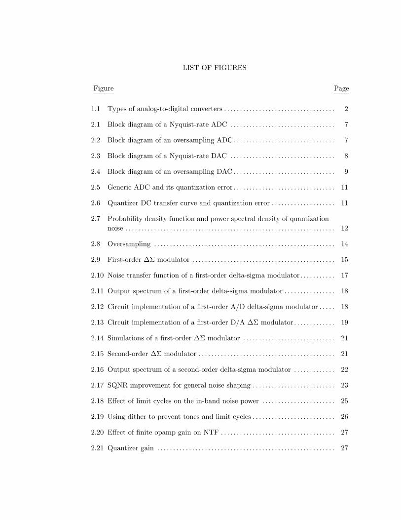
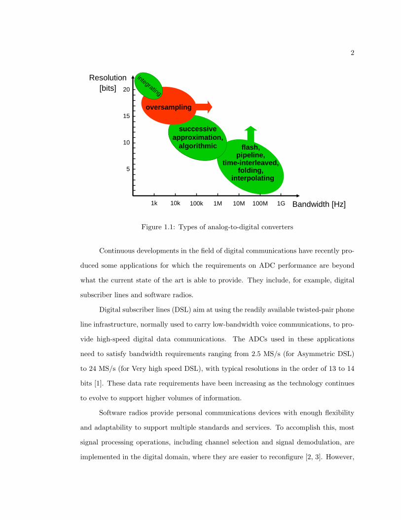
As illustrated in Fig. 1.1, a number of different ADC architectures is available
covering a wide selection of bandwidth and resolution requirements. Each of these ar-
chitectures uses a different method of operation which can be implemented efficiently for
their optimum performance range.
2
Resolution[bits]
Bandwidth [Hz]1k 10k 100k 1M 10M 100M 1G
successive approximation,
algorithmic
oversampling
integrating
5
10
15
20
flash,pipeline,
time-interleaved,folding,
interpolating
Figure 1.1: Types of analog-to-digital converters
Continuous developments in the field of digital communications have recently pro-
duced some applications for which the requirements on ADC performance are beyond
what the current state of the art is able to provide. They include, for example, digital
subscriber lines and software radios.
Digital subscriber lines (DSL) aim at using the readily available twisted-pair phone
line infrastructure, normally used to carry low-bandwidth voice communications, to pro-
vide high-speed digital data communications. The ADCs used in these applications
need to satisfy bandwidth requirements ranging from 2.5 MS/s (for Asymmetric DSL)
to 24 MS/s (for Very high speed DSL), with typical resolutions in the order of 13 to 14
bits [1]. These data rate requirements have been increasing as the technology continues
to evolve to support higher volumes of information.
Software radios provide personal communications devices with enough flexibility
and adaptability to support multiple standards and services. To accomplish this, most
signal processing operations, including channel selection and signal demodulation, are
implemented in the digital domain, where they are easier to reconfigure [2, 3]. However,
3
such a partition between the analog and digital domains puts stringent requirements on
the ADCs: they have to operate on signals that contain multiple carriers from different
sources, with large variations in RF power. For example, the ADCs used for the D-
AMPS cellular standard have to satisfy a bandwidth of 12 MHz and a resolution of 13
or 14 bits [2].
The requirements demanded by these (and other) applications have fostered re-
search in two main areas, represented by the two arrows in Fig. 1.1:
• One research direction deals with the improvement of Nyquist-rate ADCs (more
specifically, pipeline ADCs). These converters are the preferred choice for high-
speed, medium resolution performance targets. Their resolution must be enhanced,
and many techniques have been developed to accomplish that goal [4, 5, 6, 7, 8].
• The other research direction deals with the improvement of oversampling ∆Σ
ADCs. These converters are the preferred choice for low- or medium-bandwidth,
high-resolution performance targets. Their bandwidth of operation can be ex-
tended by lowering a key parameter, the oversampling ratio. However, ∆Σ ADCs
rely on high oversampling ratios to attain high-resolution and reduced sensitivity
to analog circuit components.
This thesis deals with the latter research direction, and addresses the following
challenge: how to extend the bandwidth of operation in ∆Σ ADCs without degrading
resolution, and specifically, how can that be done without resorting to high-quality analog
components.
1.2. Contributions
The three main techniques presented in this thesis are based on work proposed by
us in previous publications. They are:
4
• Low-distortion delta-sigma topologies: various forms of this technique were pre-
sented in [9, 10]. In this research, a novel low-distortion topology is introduced
[11], and shown to have other significant advantages that make it suitable for high-
bandwidth operation in MASH ADCs.
• Digital adaptive correction of leakage effects in MASH ADCs: This technique was
first proposed by [12, 13] and improved by [14]. It was further improved in the
proposed research, yielding a much smaller and simpler implementation.
• Digital estimation and correction of DAC errors: This technique was proposed in
[15, 16, 17]. It was directly implemented, basically without modifications, in the
presented research.
The main contribution of this work is the combination of these three techniques
in a three-stage MASH ADC. Since most critical design issues were shifted to the digital
domain, the performance of the implemented structure has little dependence on analog
circuit imperfections. It also shows a considerably lower power consumption than similar
designs, and the potential to reach higher speeds of operation.
1.3. Thesis Organization
Following this introduction, Chapter 2 provides the necessary background to un-
derstand the rest of the thesis. The concept of oversampling, noise-shaping and multi-
stage noise shaping are introduced and illustrated with examples. Fundamental nonideal
effects and ways to counteract them are described. Some advanced topics, not used in
this research, are also briefly discussed.
Chapter 3 describes the nonideal effects that need to be addressed to make ∆Σ
architectures suitable for wideband high-resolution operation. Current state-of-the-art
designs and their limitations are also addressed in this Chapter.

5
Chapter 4 presents three techniques that deal effectively with the described prob-
lems.
Chapter 5 proposes a MASH 2-2-2 architecture which incorporates the described
techniques.
Chapter 6 describes how to analyze noise in the proposed MASH 2-2-2 architecture.
Some key circuit parameters are calculated, based on the noise requirements.
Chapter 7 describes the circuit design in detail. The analog section of the prototype
chip is addressed here.
Chapter 8 describes the digital section of the prototype chip. It also describes its
integration with the analog section, the implementation of test modes, and the layout.
Chapter 9 describes the test setup and experimental results obtained from the
prototype chip.
Finally, Chapter 10 concludes the thesis, summarizes the contributions of this
work, and suggests ideas for future research.
6
CHAPTER 2. DELTA-SIGMA BASICS
This Chapter provides the necessary background to understand the rest of the
thesis. The concept of oversampling, noise-shaping and multi-stage noise shaping are
introduced and illustrated with examples. Fundamental nonideal effects and ways to
counteract them are described. In the interest of completeness, some advanced topics,
not used in the described research, are also briefly discussed.
2.1. Nyquist-Rate vs Oversampling Converters
In order to properly interface the analog world (composed of continuous-time,
continuous-amplitude signals) with the digital world (composed of discrete-time, discrete
amplitude signals), analog-to-digital converters require some additional signal processing
building blocks. First, the bandwidth of the input signal must be limited to half of the
sampling rate (Nyquist theorem). Otherwise, undesired higher frequency components
will alias into the band of interest, and combine with the desired signal. Therefore, a
properly named anti-alias filter (AAF) must precede any sampling operation. Also, the
input signal must be “frozen” for sufficient time, so that its amplitude can be determined.
For that reason, the ADC is also often preceded by a sample-and-hold (S/H) or track-
and-hold (T/H) block.
The block diagrams of a Nyquist-rate ADC and an oversampling ∆Σ ADC are
shown in Figure 2.1 and Figure 2.2, respectively. As illustrated in the Figures, both
analog-to-digital conversion interfaces include the described anti-alias filters and sample-
and-hold blocks. In addition, when compared with the Nyquist-rate interface, the over-
sampling interface requires some extra signal-processing steps: the analog signal is first
converted to a high-speed, low-resolution digital signal, and then filtered and down-
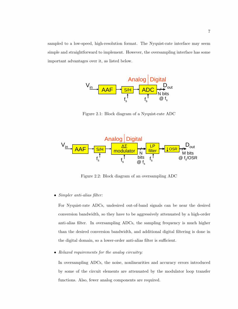
7
sampled to a low-speed, high-resolution format. The Nyquist-rate interface may seem
simple and straightforward to implement. However, the oversampling interface has some
important advantages over it, as listed below.
AAFVin Dout
Analog Digital
ADC
fsN bits@ fs
S/H
fs
Figure 2.1: Block diagram of a Nyquist-rate ADC
AAFLP
filterVin Dout
Analog Digital∆Σ
modulator OSRM bits
@ fs/OSRfs fsN
bits@ fs
S/H
fs
Figure 2.2: Block diagram of an oversampling ADC
• Simpler anti-alias filter:
For Nyquist-rate ADCs, undesired out-of-band signals can be near the desired
conversion bandwidth, so they have to be aggressively attenuated by a high-order
anti-alias filter. In oversampling ADCs, the sampling frequency is much higher
than the desired conversion bandwidth, and additional digital filtering is done in
the digital domain, so a lower-order anti-alias filter is sufficient.
• Relaxed requirements for the analog circuitry:
In oversampling ADCs, the noise, nonlinearities and accuracy errors introduced
by some of the circuit elements are attenuated by the modulator loop transfer
functions. Also, fewer analog components are required.
8
• Exchangeable speed and resolution:
Oversampling ADCs provide a flexible and robust way to meet application require-
ments. For example, for a fixed bandwidth target, the resolution can be improved
simply by operating the ADC with a higher sampling rate.
A fundamental difference distinguishing these two interface methods is that Nyquist-
rate converters are memoryless, while oversampling converters are not. Nyquist-rate
ADCs convert signals sample by sample, with each conversion independent of the previ-
ous one. In oversampling converters, the output data depends on all previous samples,
so they give a different result depending on the past history of the input signal.
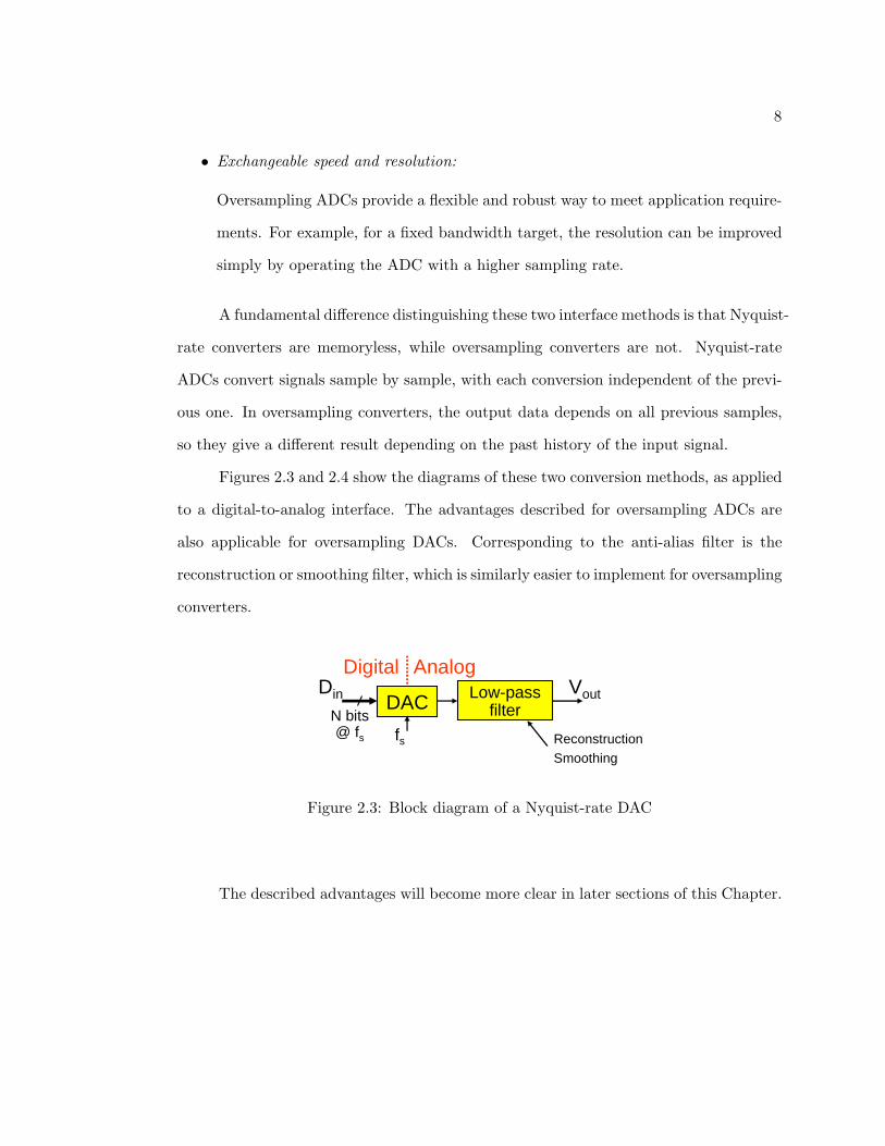
Figures 2.3 and 2.4 show the diagrams of these two conversion methods, as applied
to a digital-to-analog interface. The advantages described for oversampling ADCs are
also applicable for oversampling DACs. Corresponding to the anti-alias filter is the
reconstruction or smoothing filter, which is similarly easier to implement for oversampling
converters.
DAC Low-passfilter
Din Vout
AnalogDigital
fsN bits@ fs Reconstruction
Smoothing
Figure 2.3: Block diagram of a Nyquist-rate DAC
The described advantages will become more clear in later sections of this Chapter.

9
∆Σmodulator DAC LP
filter
Din Vout
AnalogDigital
OSRN
bits@ fs
fs fs
M bits@ fs/OSR fs
LPfilter
Figure 2.4: Block diagram of an oversampling DAC
2.2. Data Converter Performance Metrics
The mechanisms that cause performance limitations in data converters can be bet-
ter appreciated by understanding some of the parameters used in their characterization.
A brief list of these parameters is given below.
• Resolution (N): The number of bits in the output digital word.
• Bandwidth: The difference between the minimum and maximum frequencies that
can be converted by the ADC.
• Output Data Rate: The sampling frequency of the output digital word.
• Signal-to-noise-plus-distortion ratio (SNDR): The ratio between the power of the
desired signal and the combined power of all undesired contents, including all noise
sources and nonlinear effects.
• Effective Number of Bits (ENOB): The effective resolution of the converter, with
all nonideal effects included. This parameter is the equivalent in bits to the SNDR.
• Signal-to-noise ratio (SNR): The ratio between the power of the desired signal and
the power of the noise. It does not include signal harmonics.
• Dynamic Range (DR): The ratio between the maximum signal amplitude that can
be resolved without saturating the converter, and the minimum signal amplitude
that can be resolved without being mistaken for noise.
10
• Spurious Free Dynamic Range (SFDR): This parameter measures the difference
between the power of the desired signal and the power of its highest harmonic or
intermodulation products.
For Nyquist converters, it is usual to define the integral nonlinearity (INL) and
differential nonlinearity (DNL). These static parameters measure the accuracy of the
conversion on a sample-by-sample basis. As explained above, the output of an over-
sampling ∆Σ converter depends its previous state, so the INL and DNL parameters are
not meaningful. Instead, dynamic parameters such as the SNR and SNDR are used to
characterize oversampling converters.
2.3. Quantization Noise Analysis
In order to understand how ∆Σ converters operate, it is necessary first to under-
stand what is quantization noise and how it affects ADC performance. The analysis
described in this section applies to oversampling ADCs and, with small changes, to
oversampling DACs as well.
Consider the ideal ADC shown in Fig. 2.5. Its function is to convert the analog
input u into the digital equivalent v. Since the amplitude of the digital value must be
discrete, this operation introduces a quantization error, defined as the difference between
the analog equivalent of the output v and the analog input u.
Figure 2.6 shows the DC transfer curve and quantization error of this generic ADC.
Although the curves are shown for a resolution of 2 bit (N = 2), the parameters and
derivations shown in this section are applicable for any resolution1.
1It is assumed that the quantization steps are uniform. Some types of ADCs are designed to havenonlinear transfer characteristics (for example, logarithmic), but they will not be discussed in this thesis.
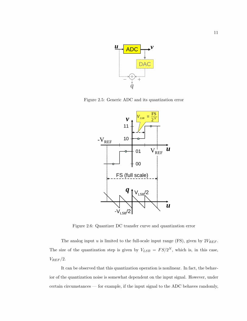
11
DAC
q
ADCu v
Figure 2.5: Generic ADC and its quantization error
NLSBV2FS=
-VREF
u
v
VREF
00
01
10
11
FS (full scale)
u
q VLSB/2
-VLSB/2
Figure 2.6: Quantizer DC transfer curve and quantization error
The analog input u is limited to the full-scale input range (FS), given by 2VREF .
The size of the quantization step is given by VLSB = FS/2N , which is, in this case,
VREF /2.
It can be observed that this quantization operation is nonlinear. In fact, the behav-
ior of the quantization noise is somewhat dependent on the input signal. However, under
certain circumstances — for example, if the input signal to the ADC behaves randomly,
12
and if the quantization steps are sufficiently small — the quantization noise can be as-
sumed to have a set of properties referred as the “additive white-noise approximation”
[18, Section 2.3]. They state that:
• The quantization noise is uncorrelated with the input signal;
• The probability density function (PDF) of the quantization noise is uniformly
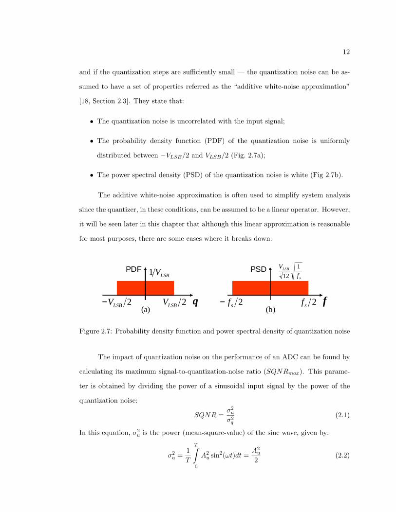
distributed between −VLSB/2 and VLSB/2 (Fig. 2.7a);
• The power spectral density (PSD) of the quantization noise is white (Fig 2.7b).
The additive white-noise approximation is often used to simplify system analysis
since the quantizer, in these conditions, can be assumed to be a linear operator. However,
it will be seen later in this chapter that although this linear approximation is reasonable
for most purposes, there are some cases where it breaks down.
q
PDFLSBV1
2LSBV− 2LSBV f
PSDs
LSB
f
V 1
12
2sf− 2sf(a) (b)
Figure 2.7: Probability density function and power spectral density of quantization noise
The impact of quantization noise on the performance of an ADC can be found by
calculating its maximum signal-to-quantization-noise ratio (SQNRmax). This parame-
ter is obtained by dividing the power of a sinusoidal input signal by the power of the
quantization noise:
SQNR =σ2
u
σ2q
(2.1)
In this equation, σ2u is the power (mean-square-value) of the sine wave, given by:
σ2u =
1T
T∫
0
A2u sin2(ωt)dt =
A2u
2(2.2)

13
and the power of the quantization error σ2q is given by:
σ2q =
1VLSB
VLSB/2∫
−VLSB/2
q2dq =V 2
LSB
12(2.3)
Alternatively, the quantization noise power can be calculated by integrating the power
spectral density from −fs/2 to +fs/2. Hence, the power spectral density can be cal-
culated as the power of the quantization noise, given in Eq. 2.3, divided by the full
bandwidth of the ADC.
For a full-scale sine wave (Au = FS/2 = VREF ), the maximum SQNR is given by:
SQNRmax =(FS/2)2/2
(FS/2N )2/12=
3222N (2.4)
Expressed in dB, this becomes Equation 2.5, which is widely used to assess the perfor-
mance of data converters.
SQNRmax[dB] = 10 log10(SQNRmax) = 6.02N + 1.76 (2.5)
2.4. Oversampling
As observed above, the total quantization noise power can be calculated by inte-
grating its power spectral density over the full bandwidth of operation of the ADC:
σ2q =
1fs
fs/2∫
−fs/2
V 2LSB
12df =
V 2LSB
12(2.6)
A simple way to improve the resolution is by using only part of the bandwidth.
This can be done by operating the ADC with a sampling frequency higher than the
Nyquist rate (fs > 2 · fB), and filtering the output to the desired bandwidth, therefore
reducing the total power of the quantization noise. This technique, illustrated on Fig. 2.8,
is called oversampling.
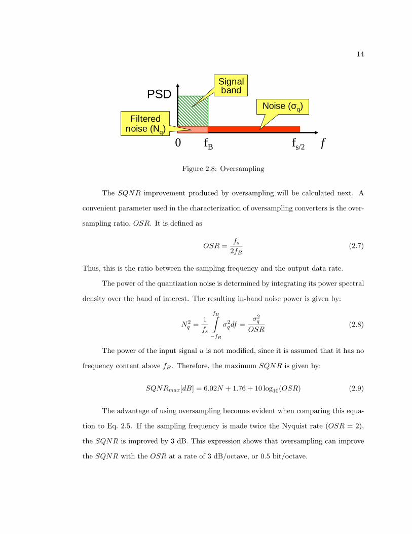
14
ffs/20 fB
Noise (σq)
Signal band
Filtered noise (Nq)
PSD
Figure 2.8: Oversampling
The SQNR improvement produced by oversampling will be calculated next. A
convenient parameter used in the characterization of oversampling converters is the over-
sampling ratio, OSR. It is defined as
OSR =fs
2fB(2.7)
Thus, this is the ratio between the sampling frequency and the output data rate.
The power of the quantization noise is determined by integrating its power spectral
density over the band of interest. The resulting in-band noise power is given by:
N2q =
1fs
fB∫
−fB
σ2qdf =
σ2q
OSR(2.8)
The power of the input signal u is not modified, since it is assumed that it has no
frequency content above fB. Therefore, the maximum SQNR is given by:
SQNRmax[dB] = 6.02N + 1.76 + 10 log10(OSR) (2.9)
The advantage of using oversampling becomes evident when comparing this equa-
tion to Eq. 2.5. If the sampling frequency is made twice the Nyquist rate (OSR = 2),
the SQNR is improved by 3 dB. This expression shows that oversampling can improve
the SQNR with the OSR at a rate of 3 dB/octave, or 0.5 bit/octave.
15
2.5. First-Order Noise Shaping
The previous section shows that oversampling can be used to trade speed for
resolution. However, speed is a limited resource, and at a rate of 3 dB/octave, plain
oversampling provides only modest improvements. It will be shown next that there are
better ways to use oversampling.
In the previous section, the quantization noise had a flat power spectral density.
A more efficient way to use oversampling is to shape the spectral density such that most
of the quantization noise power is outside of the desired signal band. A system that can
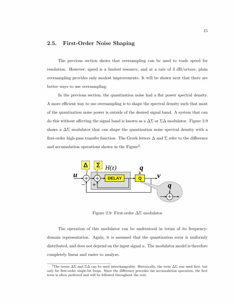
do this without affecting the signal band is known as a ∆Σ or Σ∆ modulator. Figure 2.9
shows a ∆Σ modulator that can shape the quantization noise spectral density with a
first-order high-pass transfer function. The Greek letters ∆ and Σ refer to the difference
and accumulation operations shown in the Figure2.
DELAY Qu v
q∆∆∆∆ ΣΣΣΣ H(z)
q
Figure 2.9: First-order ∆Σ modulator
The operation of this modulator can be understood in terms of its frequency-
domain representation. Again, it is assumed that the quantization error is uniformly
distributed, and does not depend on the input signal u. The modulator model is therefore
completely linear and easier to analyze.
2The terms ∆Σ and Σ∆ can be used interchangeably. Historically, the term ∆Σ was used first, butonly for first-order single-bit loops. Since the difference precedes the accumulation operation, the firstterm is often preferred and will be followed throughout the text.
16
The accumulation operation can be seen as a forward-Euler integrator, with the
transfer function:
H(z) =z−1
1− z−1(2.10)
This system has two inputs, u and q, and one output, v. Accordingly, two transfer
functions will be calculated. The signal transfer function, STF (z), is
STF (z) =V (z)U(z)
=H(z)
1 + H(z)= z−1 (2.11)
which corresponds to a single clock period delay. This means that the input signal u
appears essentially unaltered at the output v.
The noise transfer function, NTF (z), is given by
NTF (z) =V (z)Q(z)
=1
1 + H(z)= 1− z−1 (2.12)
This equation shows that the quantization error q is shaped by a first-order high-pass
transfer function. The first-order classification given to this modulator is associated with
the order of the noise transfer function.
To calculate the SQNR, it is first necessary to find the squared magnitudes of
these transfer functions, obtained for z = ejΩ. These are given by Eq. 2.13 for the
signal, and by Eq. 2.14 for the quantization error. In these equations, the normalized
angular frequency, Ω = 2πf/fs, was introduced. For convenience, it will be used instead
of the absolute frequency f , since it makes the notation simpler.
|STF |2 = |z−1|2 = 1 (2.13)
|NTF |2 = |1− z−1|2 = |1− ejΩ|2 = |1− cosΩ + j sinΩ|2
= (1− cosΩ)2 + sin2 Ω = 2− 2 cos Ω =(2 sin
Ω2
)2(2.14)
The magnitude of the noise transfer function is shown in Fig. 2.10. The in-band
noise power can now be found by integrating the power spectral density of the quantiza-
tion error — shaped by the calculated noise transfer function — in the band of interest.
This is illustrated in Fig. 2.11 and expressed in Eq. 2.15.
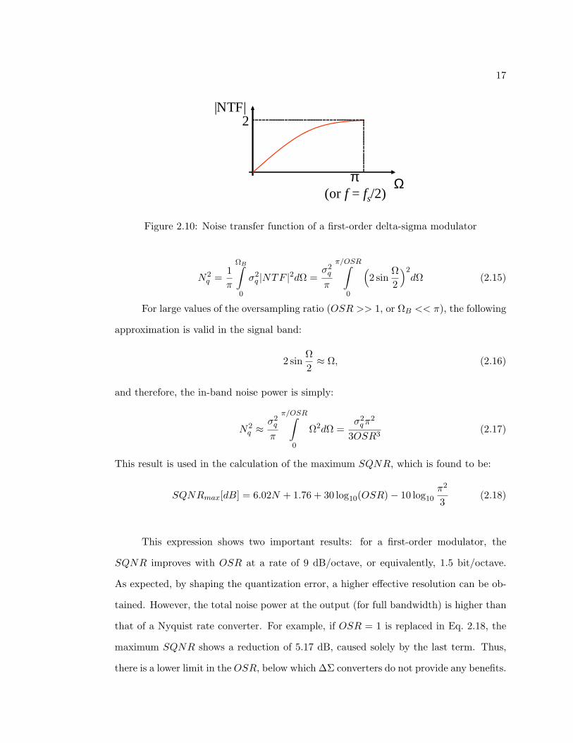
17
Ω
|NTF|
π(or f = fs/2)
2
Figure 2.10: Noise transfer function of a first-order delta-sigma modulator
N2q =
1π
ΩB∫
0
σ2q |NTF |2dΩ =
σ2q
π
π/OSR∫
0
(2 sin
Ω2
)2dΩ (2.15)
For large values of the oversampling ratio (OSR >> 1, or ΩB << π), the following
approximation is valid in the signal band:
2 sinΩ2≈ Ω, (2.16)
and therefore, the in-band noise power is simply:
N2q ≈
σ2q
π
π/OSR∫
0
Ω2dΩ =σ2
qπ2
3OSR3(2.17)
This result is used in the calculation of the maximum SQNR, which is found to be:
SQNRmax[dB] = 6.02N + 1.76 + 30 log10(OSR)− 10 log10
π2
3(2.18)
This expression shows two important results: for a first-order modulator, the
SQNR improves with OSR at a rate of 9 dB/octave, or equivalently, 1.5 bit/octave.
As expected, by shaping the quantization error, a higher effective resolution can be ob-
tained. However, the total noise power at the output (for full bandwidth) is higher than
that of a Nyquist rate converter. For example, if OSR = 1 is replaced in Eq. 2.18, the
maximum SQNR shows a reduction of 5.17 dB, caused solely by the last term. Thus,
there is a lower limit in the OSR, below which ∆Σ converters do not provide any benefits.
18
ΩπΩΒ(π/OSR)
σq2|NTF|2
Signal band
Nq2
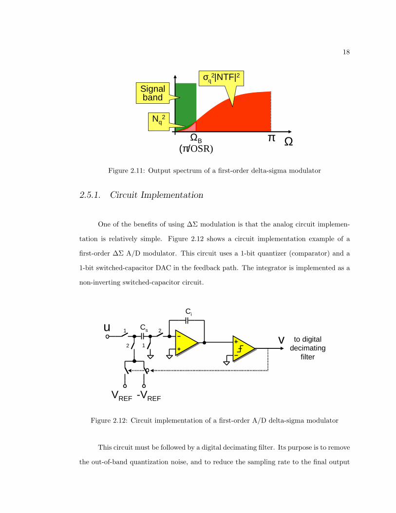
Figure 2.11: Output spectrum of a first-order delta-sigma modulator
2.5.1. Circuit Implementation
One of the benefits of using ∆Σ modulation is that the analog circuit implemen-
tation is relatively simple. Figure 2.12 shows a circuit implementation example of a
first-order ∆Σ A/D modulator. This circuit uses a 1-bit quantizer (comparator) and a
1-bit switched-capacitor DAC in the feedback path. The integrator is implemented as a
non-inverting switched-capacitor circuit.
to digital decimating
filter
21
12
Ci
Csu
VREF -VREF
v
Figure 2.12: Circuit implementation of a first-order A/D delta-sigma modulator
This circuit must be followed by a digital decimating filter. Its purpose is to remove
the out-of-band quantization noise, and to reduce the sampling rate to the final output
19
data rate used to properly represent the input signal (usually 2fB). In its simplest form,
the decimation filter can be implemented with a cascade of digital integrators running
at the sampling rate, and a cascade of differentiators running at the output data rate
[19].
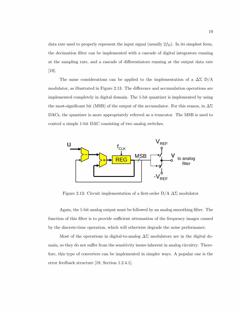
The same considerations can be applied to the implementation of a ∆Σ D/A
modulator, as illustrated in Figure 2.13. The difference and accumulation operations are
implemented completely in digital domain. The 1-bit quantizer is implemented by using
the most-significant bit (MSB) of the output of the accumulator. For this reason, in ∆Σ
DACs, the quantizer is more appropriately referred as a truncator. The MSB is used to
control a simple 1-bit DAC consisting of two analog switches.
REG
VREF
-VREF
MSB v
u
to analog filter
fCLK
Figure 2.13: Circuit implementation of a first-order D/A ∆Σ modulator
Again, the 1-bit analog output must be followed by an analog smoothing filter. The
function of this filter is to provide sufficient attenuation of the frequency images caused
by the discrete-time operation, which will otherwise degrade the noise performance.
Most of the operations in digital-to-analog ∆Σ modulators are in the digital do-
main, so they do not suffer from the sensitivity issues inherent in analog circuitry. There-
fore, this type of converters can be implemented in simpler ways. A popular one is the
error feedback structure [18, Section 1.2.4.1].
20
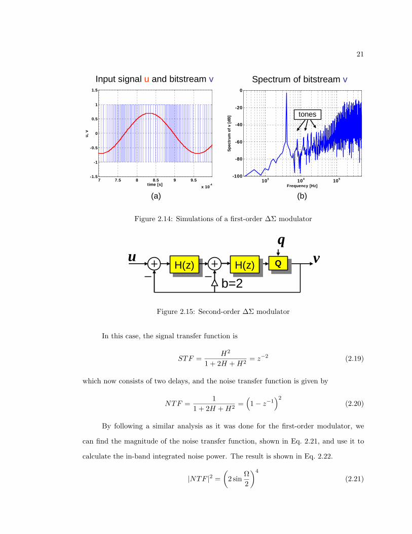
2.5.2. Simulations
To gain more insight into how noise shaping works, it is useful to observe a simu-
lation of the described first-order modulator.
Figure. 2.14a shows the time-domain behavior of the analog input u and digital
1-bit output v. The sampling frequency for this simulation was chosen as fs = 1 MHz3.
The input u is a sinusoidal wave with amplitude Au = 0.7 · VREF and frequency
fu = fs/256 ≈ 3.9 kHz. A notable detail in the Figure is that the density of pulses in
the digital output follows the amplitude of the input signal.
Figure 2.14b shows the frequency-domain behavior of the digital output v, obtained
by taking its FFT. The shape of the noise follows a 20 dB/decade slope, as expected
for a first-order system, and the tone at 3.9 kHz corresponds to the input signal. How-
ever, additional tones can be seen on this spectrum. They confirm the fact that the
quantization error is not truly random, but is correlated with the input signal.
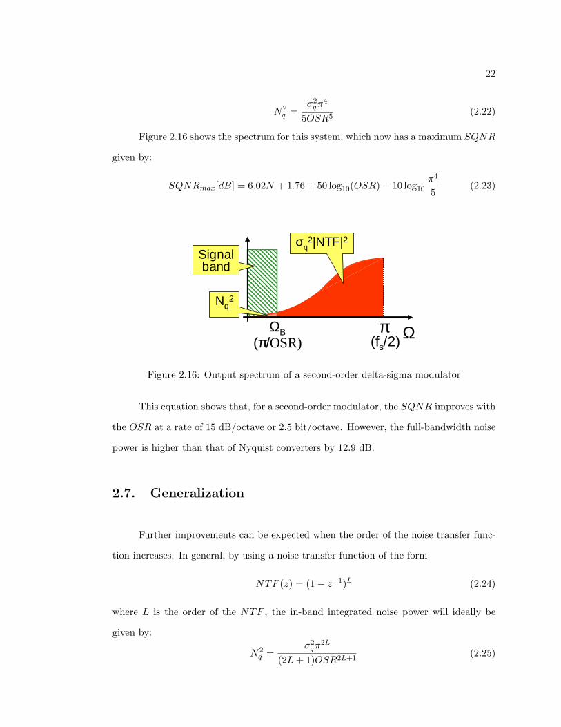
2.6. Second-Order Noise Shaping
More efficient noise shaping can be obtained by increasing the order of the noise
transfer function. The goal is to reduce the power spectral density of the quantiza-
tion error in the band of interest, at the expense of increasing it at other frequencies,
where it can be suppressed. Figure 2.15 shows the block diagram of a modulator which
implements a second-order NTF.
3This simulation does not include frequency related nonidealities, so the value used for the samplingfrequency is, in this case, irrelevant. The value used here was chosen for clarity, as an example of whatcan be used in implementations.
21
103 104 105-100
-80
-60
-40
-20
0
Frequency [Hz]
Sp
ectr
um
of
v [d
B]
7 7.5 8 8.5 9 9.5
x 10-4
-1.5
-1
-0.5
0
0.5
1
1.5
time [s]
u, v
tones
Input signal u and bitstream v Spectrum of bitstream v
(a) (b)
Figure 2.14: Simulations of a first-order ∆Σ modulator
H(z)H(z) QQu v
q
H(z)H(z)
b=2
Figure 2.15: Second-order ∆Σ modulator
In this case, the signal transfer function is
STF =H2
1 + 2H + H2= z−2 (2.19)
which now consists of two delays, and the noise transfer function is given by
NTF =1
1 + 2H + H2=
(1− z−1
)2(2.20)
By following a similar analysis as it was done for the first-order modulator, we
can find the magnitude of the noise transfer function, shown in Eq. 2.21, and use it to
calculate the in-band integrated noise power. The result is shown in Eq. 2.22.
|NTF |2 =(
2 sinΩ2
)4
(2.21)
22
N2q =
σ2qπ
4
5OSR5(2.22)
Figure 2.16 shows the spectrum for this system, which now has a maximum SQNR
given by:
SQNRmax[dB] = 6.02N + 1.76 + 50 log10(OSR)− 10 log10
π4
5(2.23)
ΩπΩΒ(π/OSR)
σq2|NTF|2
Signal band
Nq2
(fs/2)
Figure 2.16: Output spectrum of a second-order delta-sigma modulator
This equation shows that, for a second-order modulator, the SQNR improves with
the OSR at a rate of 15 dB/octave or 2.5 bit/octave. However, the full-bandwidth noise
power is higher than that of Nyquist converters by 12.9 dB.
2.7. Generalization
Further improvements can be expected when the order of the noise transfer func-
tion increases. In general, by using a noise transfer function of the form
NTF (z) = (1− z−1)L (2.24)
where L is the order of the NTF , the in-band integrated noise power will ideally be
given by:
N2q =
σ2qπ
2L
(2L + 1)OSR2L+1(2.25)
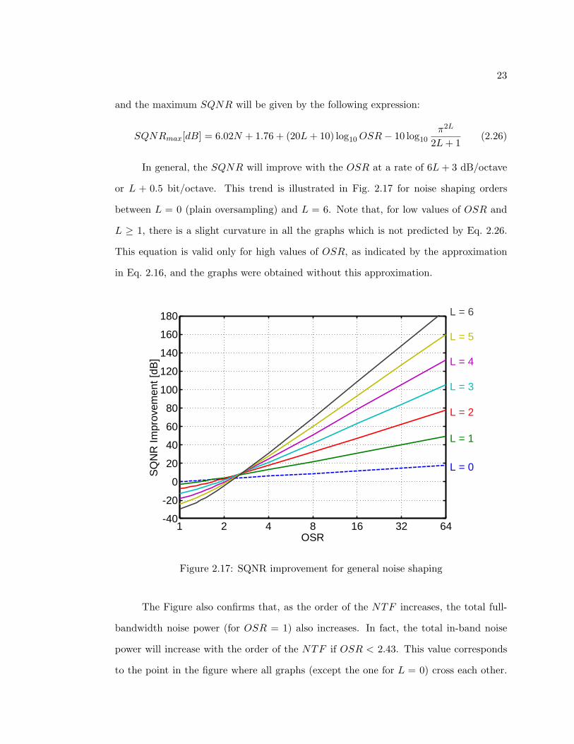
23
and the maximum SQNR will be given by the following expression:
SQNRmax[dB] = 6.02N + 1.76 + (20L + 10) log10 OSR− 10 log10
π2L
2L + 1(2.26)
In general, the SQNR will improve with the OSR at a rate of 6L + 3 dB/octave
or L + 0.5 bit/octave. This trend is illustrated in Fig. 2.17 for noise shaping orders
between L = 0 (plain oversampling) and L = 6. Note that, for low values of OSR and
L ≥ 1, there is a slight curvature in all the graphs which is not predicted by Eq. 2.26.
This equation is valid only for high values of OSR, as indicated by the approximation
in Eq. 2.16, and the graphs were obtained without this approximation.
1 2 4 8 16 32 64-40
-20
0
20
40
60
80
100
120
140
160
180
OSR
SQ
NR
Impr
ovem
ent [
dB]
L = 0
L = 1
L = 2
L = 3
L = 4
L = 5
L = 6
Figure 2.17: SQNR improvement for general noise shaping
The Figure also confirms that, as the order of the NTF increases, the total full-
bandwidth noise power (for OSR = 1) also increases. In fact, the total in-band noise
power will increase with the order of the NTF if OSR < 2.43. This value corresponds
to the point in the figure where all graphs (except the one for L = 0) cross each other.

24
This result is related with one of the key problems addressed in this thesis, and will be
discussed in more detail in Chapter 3.
2.8. Nonideal Effects
As the general expression for maximum SQNR (Eq. 2.26) indicates, there are three
parameters that can be adjusted to control the accuracy of an oversampling ADC. To
improve the SNR, one can increase the resolution of the quantizer (N), the oversampling
ratio (OSR), or the order of the noise shaping transfer function (L). However, this
equation only takes into account the random quantization error. In practice, there are
several other nonideal effects to consider. For example:
• As it was seen in Fig. 2.14b, the quantization error is not truly white. Its non-
random behavior, caused by its correlation with the input signal, is revealed by
the presence of tones and limit cycles in the output spectrum.
• The quantization error is not the only noise source. Other noise sources include
thermal noise, flicker noise, and interference noise from digital circuits.
• The noise shaping transfer function is not ideal. For ADC implementations, circuit
imperfections such as capacitor mismatches and finite opamp gain limit the ability
to suppress in-band noise.
Two other nonideal effects deserve special attention: the first one has to do with
the ability to use multibit quantizers (with N > 1). The linearity of the corresponding
multibit feedback DAC is limited, and it directly affects the overall accuracy of the ADC.
This topic will be discussed in more detail in the next Chapter. The second nonideal
effect has to do with stability: higher-order loops (with L > 2) have the potential to
become unstable.
All these nonideal effects will be described in more detail next.
25
2.8.1. Tones and Limit Cycles
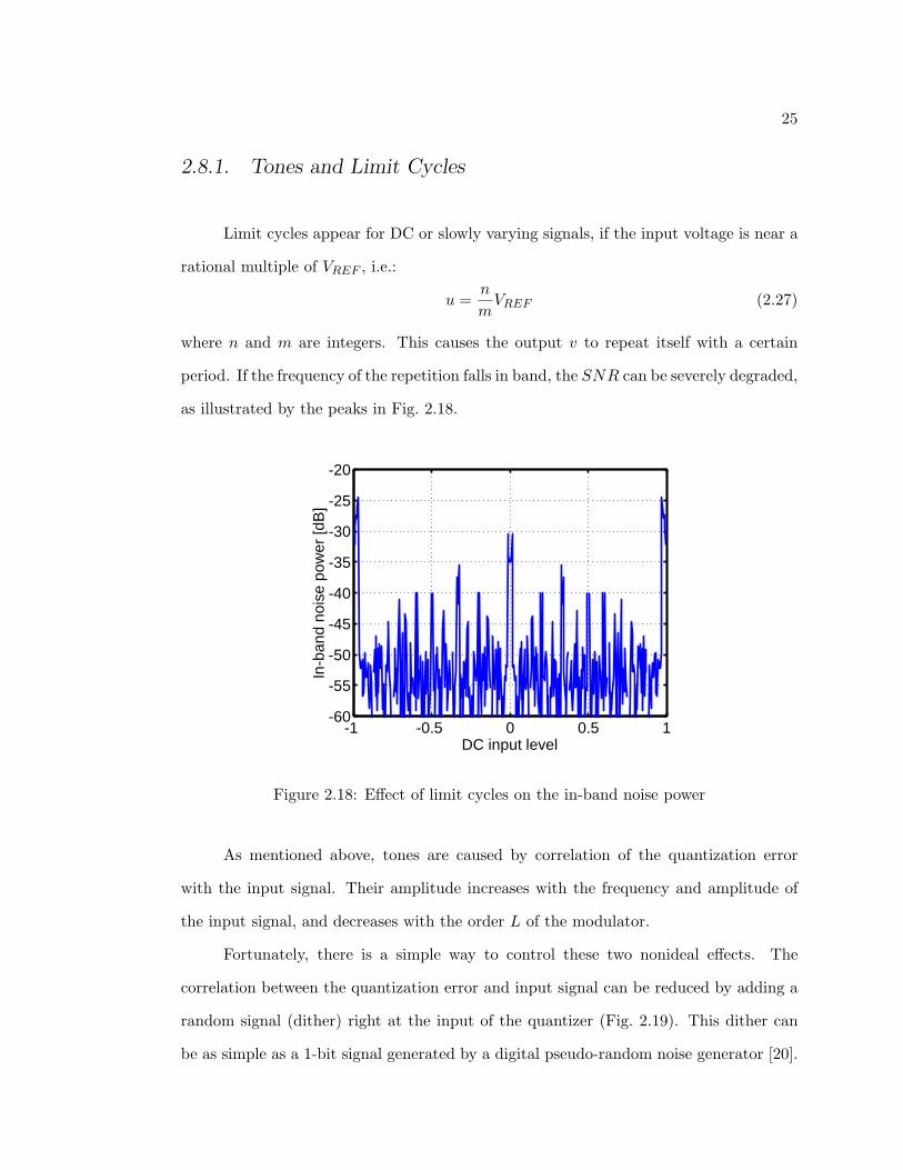
Limit cycles appear for DC or slowly varying signals, if the input voltage is near a
rational multiple of VREF , i.e.:
u =n
mVREF (2.27)
where n and m are integers. This causes the output v to repeat itself with a certain
period. If the frequency of the repetition falls in band, the SNR can be severely degraded,
as illustrated by the peaks in Fig. 2.18.
-1 -0.5 0 0.5 1-60
-55
-50
-45
-40
-35
-30
-25
-20
DC input level
In-b
and
nois
e po
wer
[dB
]
Figure 2.18: Effect of limit cycles on the in-band noise power
As mentioned above, tones are caused by correlation of the quantization error
with the input signal. Their amplitude increases with the frequency and amplitude of
the input signal, and decreases with the order L of the modulator.
Fortunately, there is a simple way to control these two nonideal effects. The
correlation between the quantization error and input signal can be reduced by adding a
random signal (dither) right at the input of the quantizer (Fig. 2.19). This dither can
be as simple as a 1-bit signal generated by a digital pseudo-random noise generator [20].
26
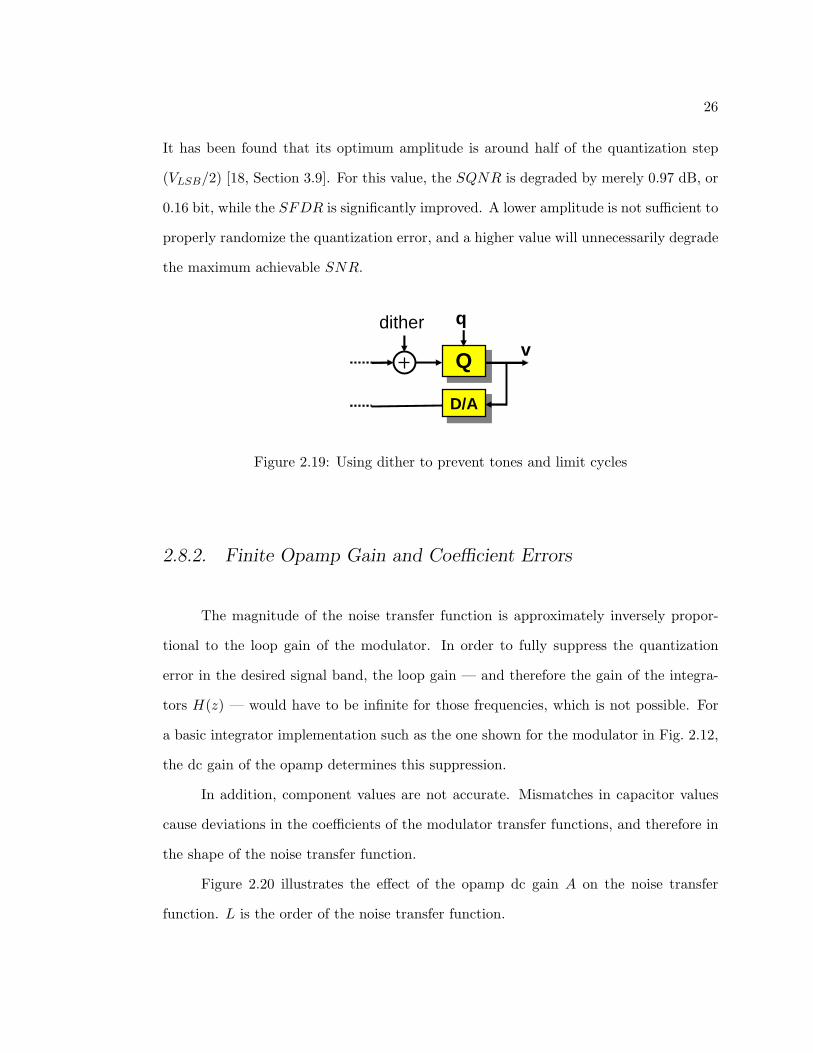
It has been found that its optimum amplitude is around half of the quantization step
(VLSB/2) [18, Section 3.9]. For this value, the SQNR is degraded by merely 0.97 dB, or
0.16 bit, while the SFDR is significantly improved. A lower amplitude is not sufficient to
properly randomize the quantization error, and a higher value will unnecessarily degrade
the maximum achievable SNR.
D/AD/A
v
qdither
Figure 2.19: Using dither to prevent tones and limit cycles
2.8.2. Finite Opamp Gain and Coefficient Errors
The magnitude of the noise transfer function is approximately inversely propor-
tional to the loop gain of the modulator. In order to fully suppress the quantization
error in the desired signal band, the loop gain — and therefore the gain of the integra-
tors H(z) — would have to be infinite for those frequencies, which is not possible. For
a basic integrator implementation such as the one shown for the modulator in Fig. 2.12,
the dc gain of the opamp determines this suppression.
In addition, component values are not accurate. Mismatches in capacitor values
cause deviations in the coefficients of the modulator transfer functions, and therefore in
the shape of the noise transfer function.
Figure 2.20 illustrates the effect of the opamp dc gain A on the noise transfer
function. L is the order of the noise transfer function.

27
|NTF|
ΩIdeal opamps
Real opamps
1/AL Slope = 6L dB/octave
Figure 2.20: Effect of finite opamp gain on NTF
2.8.3. Stability
One of the assumptions regarding the operation of the quantizer, besides from
being linear, is that it has a fixed gain. This gain, shown as k in Fig. 2.21, can be
defined as the ratio between the mean square value of the quantizer output and that of
its input [18, Section 4.2.1]:
k =cov(v, y)cov(y, y)
(2.28)
However, when the nonlinear nature of the quantizer is taken into account, it
can be observed that this gain is not well defined. This is more pronounced for single-
bit quantizers, where the input can take any value but the output jumps between two
levels only. In this case, the gain k is arbitrary, and it is the feedback operation of the
modulator loop that determines what its value should be.
H(z)u v
qky
Figure 2.21: Quantizer gain

28
For first- and second-order modulator loops, variations in the gain of the quantizer
do not cause problems, other than a temporary reduction of performance. However, for
higher-order modulators, there are forbidden values for k. If reached, they will cause the
modulator to become unstable.
One way to see how the quantizer gain can affect the stability of a high-order
modulator (but not of a second-order one) is shown in Figure 2.22. This Figure shows
the z-plane root-locus representation of the NTF’s poles and zeros.
k=1
k=0
k=0.5L=3
Unstable for k < 0.5
k=1 k=0
L=2
Always stable
Figure 2.22: Stability
For both the second-order and third-order noise transfer functions, the zeros are
located at DC, or z = 1. For normal operation, k = 1, in which case both NTFs have
their poles at z = 0. As the quantizer gain k changes between 1 and 0, the poles of
the second-order NTF remain always inside the unit circle, satisfying the condition for
stability. However, for the third-order NTF, the poles go outside the circle for part of
the root locus. If k < 0.5, the modulator is unstable. In this situation, the output v will
spend more and more time at 1 or -1, causing the internal states of the modulator (the
integrator outputs) to grow until they saturate.
29
The gain k will be small if the signal y, at the quantizer input, is too large. There
are two mechanisms that can cause this to happen: if the modulator input signal u is
too strong, or if the power of the out-of-band quantization error is too high.
Not much can be done about the input signal amplitude besides from constraining
it to a smaller range. However, the probability of unstable behavior can be minimized
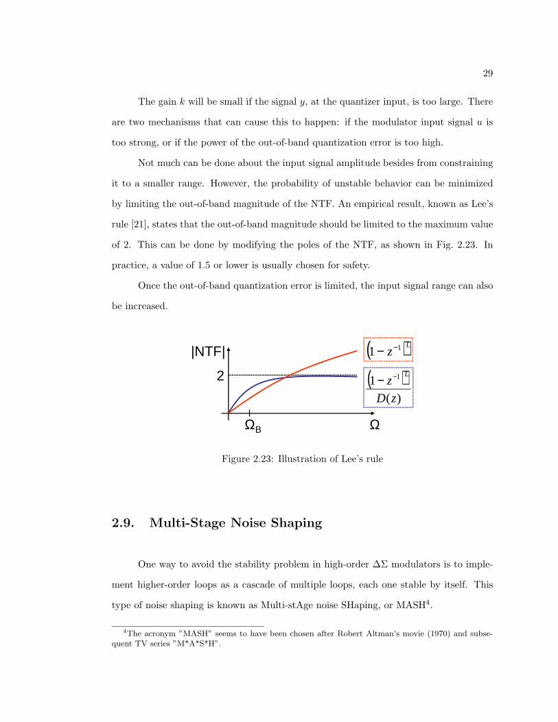
by limiting the out-of-band magnitude of the NTF. An empirical result, known as Lee’s
rule [21], states that the out-of-band magnitude should be limited to the maximum value
of 2. This can be done by modifying the poles of the NTF, as shown in Fig. 2.23. In
practice, a value of 1.5 or lower is usually chosen for safety.
Once the out-of-band quantization error is limited, the input signal range can also
be increased.
( ))(
1 1
zD
zL−−
Ω
( )Lz 11 −−
ΩΒ
|NTF|
2
Figure 2.23: Illustration of Lee’s rule
2.9. Multi-Stage Noise Shaping
One way to avoid the stability problem in high-order ∆Σ modulators is to imple-
ment higher-order loops as a cascade of multiple loops, each one stable by itself. This
type of noise shaping is known as Multi-stAge noise SHaping, or MASH4.
4The acronym ”MASH” seems to have been chosen after Robert Altman’s movie (1970) and subse-quent TV series ”M*A*S*H”.

30
2.9.1. Theory of Operation
Figure 2.24 shows a general MASH structure. The first stage (ADC1) is a ∆Σ
modulator; each of the remaining stages (ADC2 to ADCn) can use a ∆Σ modulator as
well, or a plain Nyquist-rate ADC. If the quantization error q produced by each stage
is acquired and converted to digital format by a subsequent ADC stage, that error can
be cancelled out at the MASH output v, therefore increasing the total accuracy of the
converter.
u v1
DigitalError
Cancellation Logic
v
ADC1(STF1, NTF1)
q1
v2ADC2(STF2, NTF2)
…ADCn
(STFn, NTFn)qn-1
vn
Figure 2.24: MASH diagram
The purpose of the error cancellation logic is to cancel the quantization noise from
all stages except the last, so that:
V = U · STF1STF2 . . . STFn + Qn ·NTF1NTF2 . . . NTFn (2.29)
The order of the noise transfer function is the sum of the individual orders, L1 to Ln. As
long as each stage uses second-order (or lower) noise shaping, the structure is guaranteed
to be stable. Ideally, the equivalent quantizer resolution is the sum of the individual
quantizer resolutions, N1 to Nn. In practice, signal scaling requirements cause it to be
somewhat smaller.

31
This technique is akin to two-step or pipeline ADCs, where the input signal is
converted by a coarse ADC to get the most-significant bits (MSBs), and the residue
(quantization error) is converted by a subsequent ADC (or ADCs) to get the least-
significant bits (LSBs). The outputs of all stages are then combined to obtain a finer
resolution.
When referring to a MASH ADC, it is usual to indicate the number of stages and
the order of each stage. For example, a MASH 2-0 has two stages: the first stage is a
second-order modulator, and the second stage is a zero-order (not noise shaping) ADC.
A diagram of such a structure is shown in Figure 2.25.
H(z)H(z) H(z)H(z) QQ
D/AD/A2
u v1
q1
q1 DNTF(z)DNTF(z)
v
A/DA/Dv2
q2
Figure 2.25: MASH 2-0 diagram
The quantization error q1 is obtained by subtracting the output of the quantizer
from its input. For this example, the output v of the structure is given by:
V = U · STF1 + Q1 · (ANTF −DNTF )−Q2 ·DNTF (2.30)
where ANTF is the noise transfer function of the first stage, implemented in analog do-
main, and DNTF is the noise transfer function following the second stage, implemented
in digital domain. Assuming that everything is ideal, i.e., that DNTF = ANTF ,
the quantization error q1 is cancelled, and only the second-stage’s quantization noise q2,
shaped by DNTF , will be present at the output:
V = U · STF1 −Q2 ·DNTF (2.31)

32
If the transfer functions do not match exactly, a problem known as quantization
noise leakage will occur. This is explained in detail in the next Chapter.
2.10. Advanced Topics
There are many different topics that were not explored in the proposed research,
and therefore were not covered in this chapter. However, to be complete, a brief descrip-
tion of these topics is provided in this section.
• Decimation Filter Implementation:
In its simplest form, a sinc filter with order L+1 is all that is required to properly
remove the out-of-band quantization error, and it can be implemented as a cascade
of integrators and differentiators [19].
• Optimization of Zeros:
The noise transfer functions discussed in this thesis have all their zeros at DC.
Since, in practice, the noise in the baseband is — for the most part — dominated
by other noise sources, there are benefits in allowing some extra quantization noise
in the lower frequencies (therefore reducing it at the higher end of the baseband,
where it becomes dominant). This can be accomplished by spreading the zeros
of the noise transfer function. The result is a small but in some cases significant
improvement in the SNDR.
• Bandpass ∆Σ Converters:
Only low-pass ∆Σ modulators, with the desired signal band centered at DC, are
discussed in this thesis. The loop filter is implemented with integrators, since they
provide their highest gain at DC. In a number of applications (typically for commu-
nication systems), the desired signal band is centered at other frequencies. Thus,
33
the loop filter is implemented with resonators, with their highest gain centered at
those frequencies.
• Complex ∆Σ Converters:
All transfer functions shown in this thesis have complex conjugate poles, so they
have magnitude responses which are symmetric around DC. In some communi-
cation applications, such as in direct conversion receivers, it is often desirable to
implement asymmetric transfer functions. Complex or quadrature ∆Σ modulators
[22] are implemented with two channels operating on I and Q (real and imaginary)
input signals. The resonators used in these modulators can place a single complex
pole anywhere in the unit circle.
• Continuous-Time ∆Σ Converters:
In a continuous time modulator, the integrators or resonators are implemented as
active RC or LC filters, and are not switched. The sampling operation is usu-
ally done right at the quantizer. Therefore, continuous-time ∆Σ modulators can
operate at higher frequencies and with lower power than their discrete-time coun-
terparts. Also, the anti-alias filter can be included in the signal transfer function.
However, continuous-time ∆Σ converters are sensitive to clock-jitter issues origi-
nating in the feedback DAC.
34
CHAPTER 3. PROBLEMS IN WIDEBAND MASH
ADCS
This Chapter describes the nonideal effects that need to be addressed to make ∆Σ
architectures suitable for wideband high-resolution operation. Current state-of-the-art
designs and their limitations are also addressed.
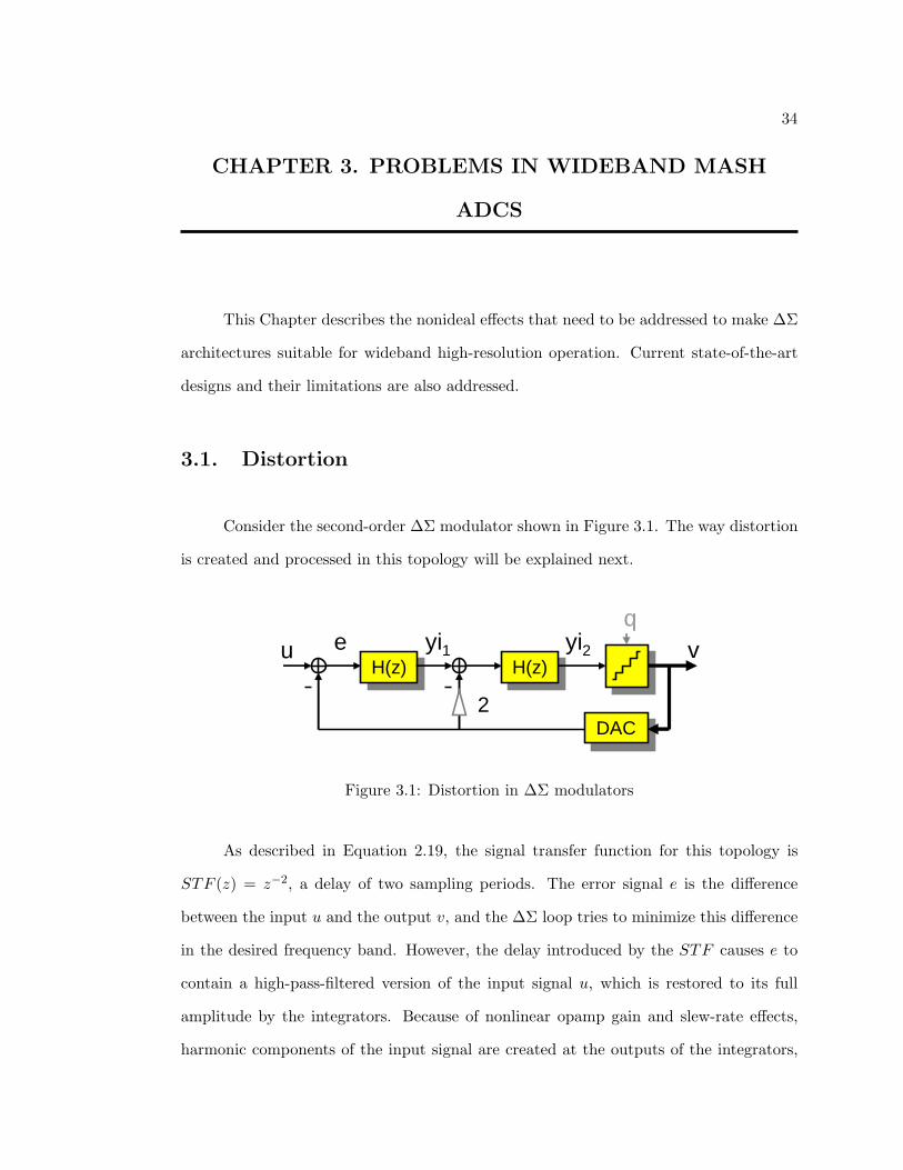
3.1. Distortion
Consider the second-order ∆Σ modulator shown in Figure 3.1. The way distortion
is created and processed in this topology will be explained next.
H(z)H(z) H(z)H(z)u vyi1 yi2
2DACDAC
qe
Figure 3.1: Distortion in ∆Σ modulators
As described in Equation 2.19, the signal transfer function for this topology is
STF (z) = z−2, a delay of two sampling periods. The error signal e is the difference
between the input u and the output v, and the ∆Σ loop tries to minimize this difference
in the desired frequency band. However, the delay introduced by the STF causes e to
contain a high-pass-filtered version of the input signal u, which is restored to its full
amplitude by the integrators. Because of nonlinear opamp gain and slew-rate effects,
harmonic components of the input signal are created at the outputs of the integrators,

35
in yi1 and yi2, and will appear at the output of the modulator in v, shaped by first- and
second-order high-pass transfer functions, respectively, as illustrated in Fig. 3.2.
10-2
10-1
-80
-70
-60
-50
-40
-30
-20
-10
0
10
20
Normalized Frequency (fs = 1)
Mag
nitu
de [d
B]
OSR=8
V/Yi1
V/Yi2
OSR=128
Figure 3.2: Transfer functions from the integrator outputs to the modulator output
As the figure shows, the attenuation provided by these transfer functions is satis-
factory if a high oversampling ratio is used. For example, if OSR = 128, harmonics in
the output of the first integrator, yi1, will be reduced by at least 32.2 dB. However, if
OSR = 8, the attenuation is only 8.2 dB. In wideband applications, where high-speed
analog signal processing blocks are required, designing a sufficiently low distortion opamp
to deal with this problem can be impractical.
Figure 3.3 shows the simulated spectra of this second-order modulator, illustrating
its shortcomings for wideband operation. The modulator uses an ideal 6-bit quantizer
and DAC. The model used for the integrators incorporates a nonlinear opamp input-
output transfer curve, in the form of a hyperbolic tangent with a maximum gain of
50 dB. The input signal frequency is at fu = fs/32, and its amplitude is Au = 0.9 V.

36
Frequency [Hz]
Sp
ectr
um
of
v [d
B]
Sp
ectr
um
of
yi1
[dB
]S
pec
tru
m o
fyi
2
[dB
]
10k 100k 1M 10M
10k 100k 1M 10M
10k 100k 1M 10M
0
-50
-100
-150
0
-50
-100
-150
0
-50
-100
-150
Figure 3.3: Simulation for nonlinear opamp gain
The output of the first and second integrators show the presence of the input
signal, together with harmonics created due to the nonlinear opamp gain curve. The
output v shows a third harmonic with an amplitude of -57.3 dB below the fundamental.
This value can be improved by reducing the input signal amplitude, or by using properly
scaled integrator coefficients, to reduce the voltage swing at their outputs. However, in
the first case, the input dynamic range of the modulator is sacrificed. In the second case,
larger capacitances are required, sacrificing area and power consumption.
3.2. Matching of Analog and Digital NTFs
Figure 3.4 shows again the MASH 2-0 structure described in Section 2.9. As pre-
viously explained, the output v of the structure is given by
V = U · STF1 + Q1 · (ANTF −DNTF )−Q2 ·DNTF (3.1)

37
and as long as ANTF = DNTF , the quantization error q1 is cancelled at the output.
H(z)H(z) H(z)H(z) QQ
D/AD/A2
u v1
q1
q1 DNTF(z)DNTF(z)
v
A/DA/Dv2
q2
Figure 3.4: MASH 2-0 diagram
However, in practice, it is not possible to make ANTF exactly the same as DNTF .
ANTF is an analog transfer function, subject to analog circuit imperfections, while
DNTF is a digital transfer function. Any mismatch between them will cause some of
the quantization error q1 to appear at the output v. This problem, known as quantization
noise leakage, is illustrated by the simulations in Figure 3.5.
0
-50
-100
-150
-2000.50.10.01
Normalized frequency (to fs)
Out
put s
pect
rum
[dB
]
DNTF matches ANTF0
-50
-100
-150
-2000.50.10.010.001
Normalized frequency (to fs)
Out
put s
pect
rum
[dB
] 0.1% mismatch in ANTF
Figure 3.5: Effect of mismatches between the analog and digital noise transfer functions
In the ideal case (DNTF matches ANTF ), q1 is perfectly cancelled at the output,
so the spectrum shows only the quantization error q2 shaped by the digital second-order
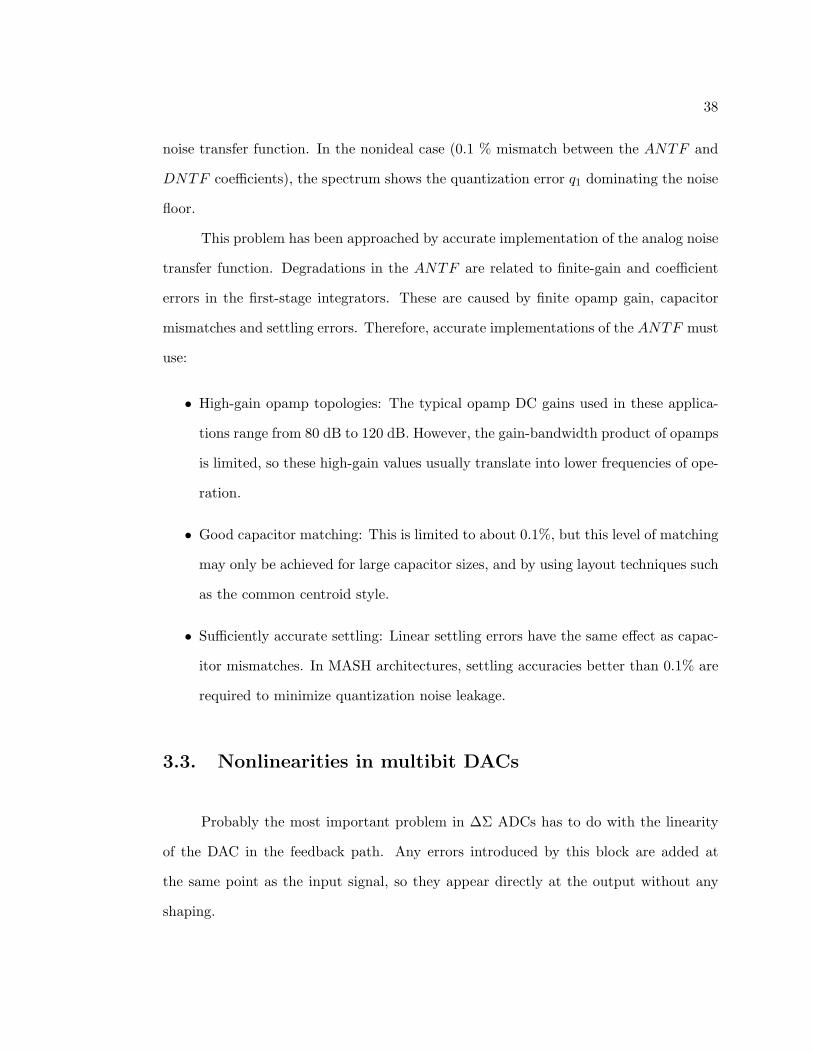
38
noise transfer function. In the nonideal case (0.1 % mismatch between the ANTF and
DNTF coefficients), the spectrum shows the quantization error q1 dominating the noise
floor.
This problem has been approached by accurate implementation of the analog noise
transfer function. Degradations in the ANTF are related to finite-gain and coefficient
errors in the first-stage integrators. These are caused by finite opamp gain, capacitor
mismatches and settling errors. Therefore, accurate implementations of the ANTF must
use:
• High-gain opamp topologies: The typical opamp DC gains used in these applica-
tions range from 80 dB to 120 dB. However, the gain-bandwidth product of opamps
is limited, so these high-gain values usually translate into lower frequencies of ope-
ration.
• Good capacitor matching: This is limited to about 0.1%, but this level of matching
may only be achieved for large capacitor sizes, and by using layout techniques such
as the common centroid style.
• Sufficiently accurate settling: Linear settling errors have the same effect as capac-
itor mismatches. In MASH architectures, settling accuracies better than 0.1% are
required to minimize quantization noise leakage.
3.3. Nonlinearities in multibit DACs
Probably the most important problem in ∆Σ ADCs has to do with the linearity
of the DAC in the feedback path. Any errors introduced by this block are added at
the same point as the input signal, so they appear directly at the output without any
shaping.
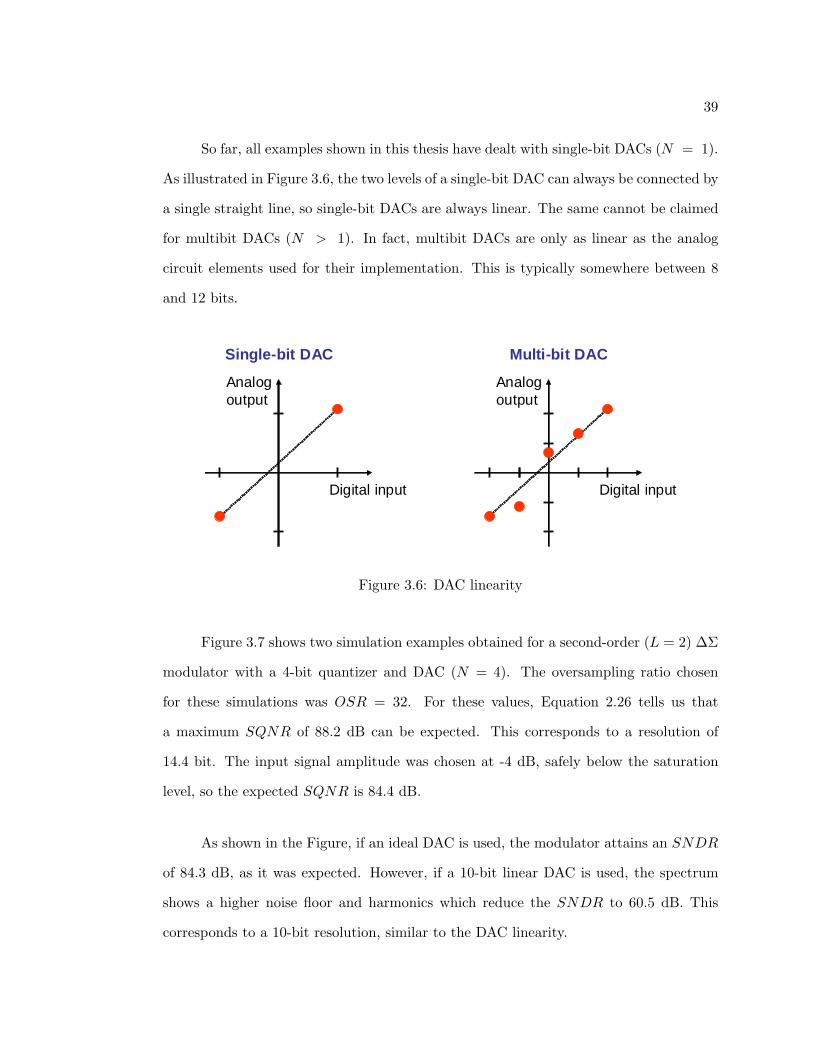
39
So far, all examples shown in this thesis have dealt with single-bit DACs (N = 1).
As illustrated in Figure 3.6, the two levels of a single-bit DAC can always be connected by
a single straight line, so single-bit DACs are always linear. The same cannot be claimed
for multibit DACs (N > 1). In fact, multibit DACs are only as linear as the analog
circuit elements used for their implementation. This is typically somewhere between 8
and 12 bits.
Digital input
Analog output
Single-bit DAC
Digital input
Analog output
Multi-bit DAC
Figure 3.6: DAC linearity
Figure 3.7 shows two simulation examples obtained for a second-order (L = 2) ∆Σ
modulator with a 4-bit quantizer and DAC (N = 4). The oversampling ratio chosen
for these simulations was OSR = 32. For these values, Equation 2.26 tells us that
a maximum SQNR of 88.2 dB can be expected. This corresponds to a resolution of
14.4 bit. The input signal amplitude was chosen at -4 dB, safely below the saturation
level, so the expected SQNR is 84.4 dB.
As shown in the Figure, if an ideal DAC is used, the modulator attains an SNDR
of 84.3 dB, as it was expected. However, if a 10-bit linear DAC is used, the spectrum
shows a higher noise floor and harmonics which reduce the SNDR to 60.5 dB. This
corresponds to a 10-bit resolution, similar to the DAC linearity.
40
0.50.10.010.001Normalized frequency
0
-150
-50
-100
Ideal DAC
SNDR=84.3 dB[d
B]
0.50.10.010.001Normalized frequency
0
-150
-50
-100
10-bit linear DAC
SNDR=60.5 dB
[dB
]
Figure 3.7: Effect of DAC nonlinearities on ADC performance
This example shows that the linearity of a ∆Σ modulator cannot be better than
the linearity of the DAC used in its feedback path. Therefore, if multibit DACs are to
be employed, something must be done to improve their linearity.
For some time, the only solution to this problem was to perform calibration of the
DAC elements. The direct way was to do this during fabrication, for example, by using
laser trimming. This technique is expensive, and does not account for long-term process
variations caused by temperature and aging.
A more reliable solution is to perform calibration during circuit operation. Several
calibration techniques exist that correct for element mismatch. They work by measuring
and correcting the error of each DAC element, with additional analog or mixed ana-
log/digital circuitry — in some cases, an additional high-resolution, very low-bandwidth
ADC is used. These calibration cycles can be performed periodically to account for long-
term variations, but they usually require the system to be off-line during the calibration
time. They also increase analog design difficulty.
A very popular DAC linearization technique is Dynamic Element Matching (DEM)
[23, 24]. The idea is to randomize the usage of the DAC unit elements, so that the
mismatch errors are averaged or shaped. Many different DEM algorithms are available.
A few of them are listed below:
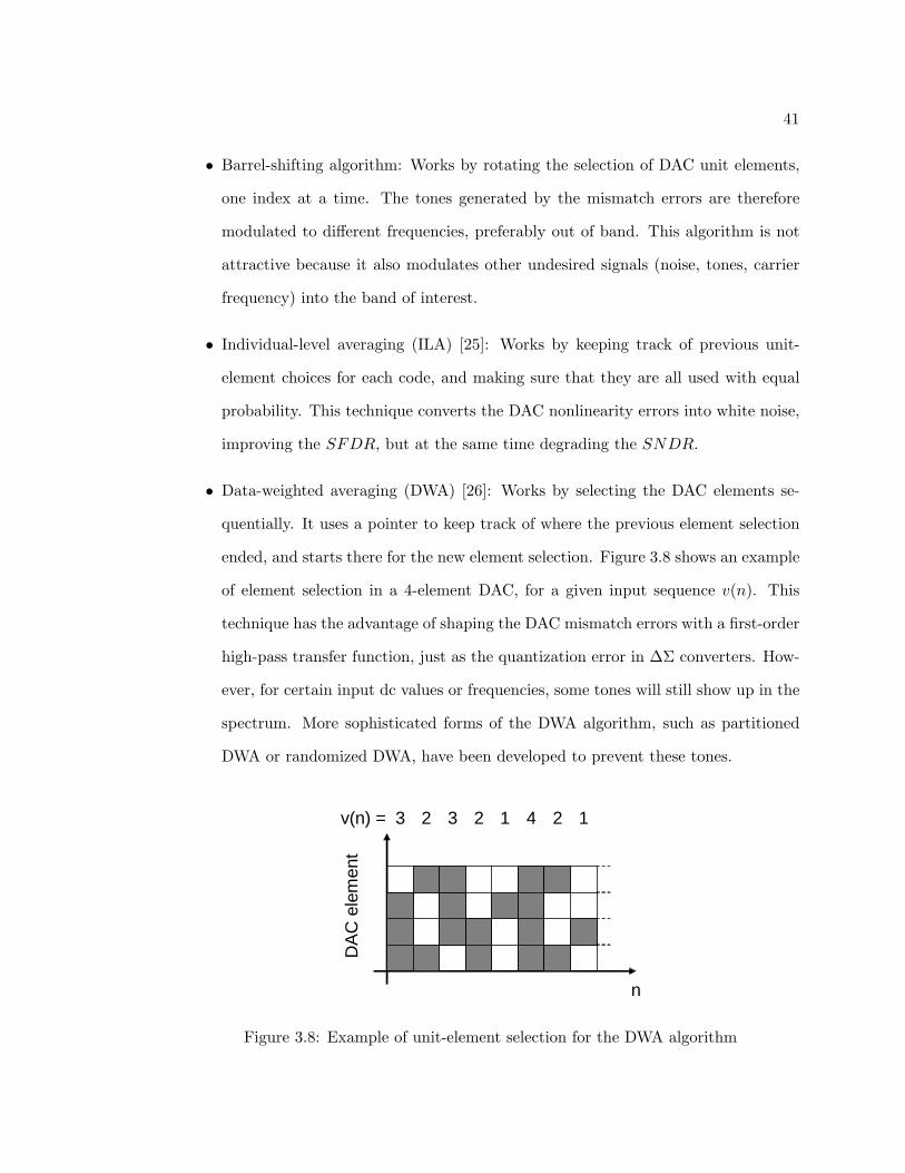
41
• Barrel-shifting algorithm: Works by rotating the selection of DAC unit elements,
one index at a time. The tones generated by the mismatch errors are therefore
modulated to different frequencies, preferably out of band. This algorithm is not
attractive because it also modulates other undesired signals (noise, tones, carrier
frequency) into the band of interest.
• Individual-level averaging (ILA) [25]: Works by keeping track of previous unit-
element choices for each code, and making sure that they are all used with equal
probability. This technique converts the DAC nonlinearity errors into white noise,
improving the SFDR, but at the same time degrading the SNDR.
• Data-weighted averaging (DWA) [26]: Works by selecting the DAC elements se-
quentially. It uses a pointer to keep track of where the previous element selection
ended, and starts there for the new element selection. Figure 3.8 shows an example
of element selection in a 4-element DAC, for a given input sequence v(n). This
technique has the advantage of shaping the DAC mismatch errors with a first-order
high-pass transfer function, just as the quantization error in ∆Σ converters. How-
ever, for certain input dc values or frequencies, some tones will still show up in the
spectrum. More sophisticated forms of the DWA algorithm, such as partitioned
DWA or randomized DWA, have been developed to prevent these tones.
n
DA
C e
lem
ent
3 2 3 2 1 4 2 1v(n) =
Figure 3.8: Example of unit-element selection for the DWA algorithm
42
• Tree-structure methods: This technique allows for great flexibility in the selection
of DAC unit elements [27]. Multiple layers of switching blocks, arranged in a tree
fashion, allow for each unit element to be independently selected. Any of the
algorithms described above, or more sophisticated ones, can be implemented by
proper control of the switching blocks.
All these techniques have a characteristic in common. They do not eliminate DAC
errors. They work by randomizing or shaping the errors, therefore improving system
performance, but the mismatch errors are still present in the output spectrum. Their
energy is either in-band, in a less harmful form, or out of band.
For wideband ∆Σ conversion, where low oversampling ratio values need to be used,
it is even more difficult to randomize or shape the DAC errors.
3.4. Traditional Solutions (State of the Art)
A list with some of the published ∆Σ converters designed to satisfy high-resolution
and wide bandwidth specifications is shown in Table 3.1. Three of the highest-performance
MASH designs in this list are included in Table 3.2 below, revealing more details about
their structure and performance.
All these circuits require high-quality analog components. One case in point is the
performance of the opamp used in the first integrator. This is the most critical opamp
in ∆Σ ADC converters, because it has to drive the largest capacitances, and its noise
and distortion is the least suppressed by the modulator loop:
• In [Fujimori ’00], the first opamp was implemented in a folded cascode topology
with gain boosting, achieving a DC gain of 96 dB.
• For [Vleugels ’01], the first opamp contains a simple (wideband) preamplifier stage
followed by a cascode stage. The cascode transistors also use amplifiers for gain
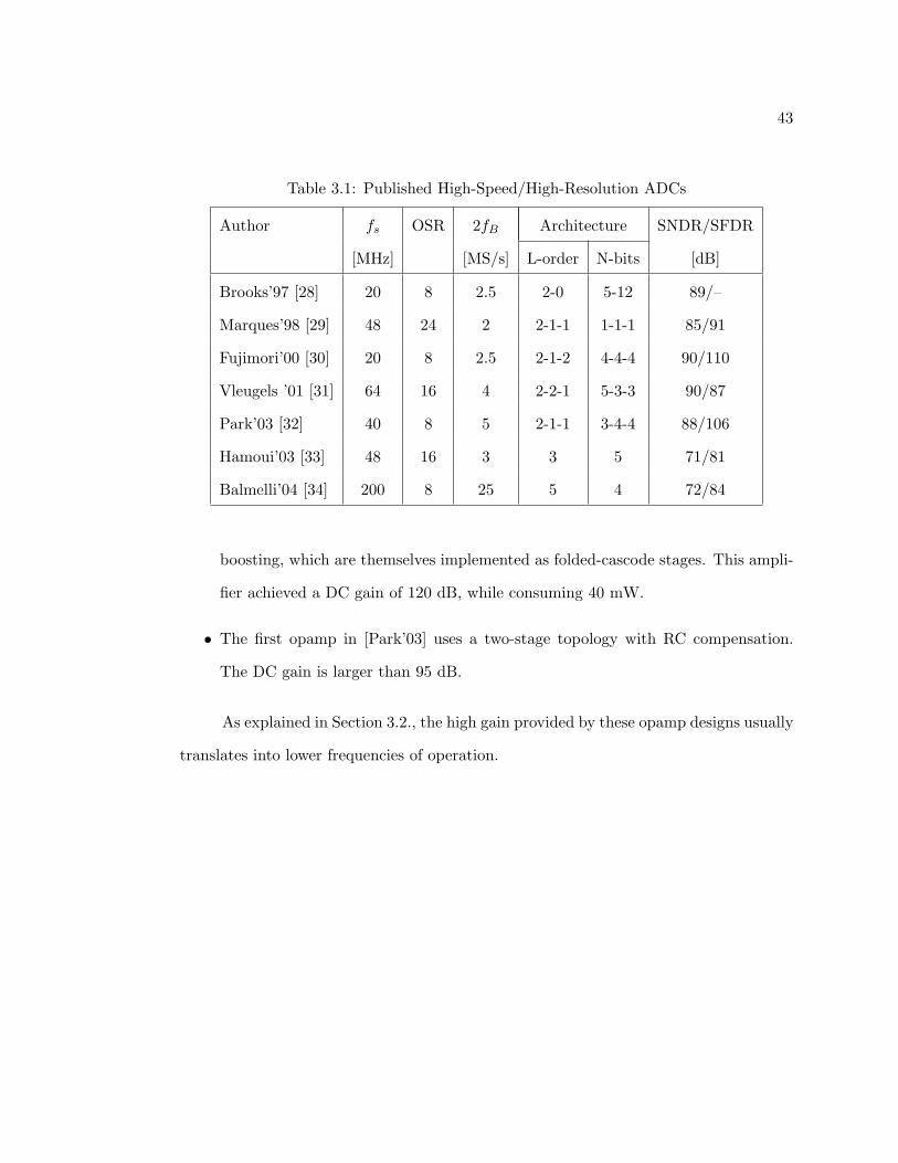
43
Table 3.1: Published High-Speed/High-Resolution ADCs
Author fs OSR 2fB Architecture SNDR/SFDR
[MHz] [MS/s] L-order N-bits [dB]
Brooks’97 [28] 20 8 2.5 2-0 5-12 89/–
Marques’98 [29] 48 24 2 2-1-1 1-1-1 85/91
Fujimori’00 [30] 20 8 2.5 2-1-2 4-4-4 90/110
Vleugels ’01 [31] 64 16 4 2-2-1 5-3-3 90/87
Park’03 [32] 40 8 5 2-1-1 3-4-4 88/106
Hamoui’03 [33] 48 16 3 3 5 71/81
Balmelli’04 [34] 200 8 25 5 4 72/84
boosting, which are themselves implemented as folded-cascode stages. This ampli-
fier achieved a DC gain of 120 dB, while consuming 40 mW.
• The first opamp in [Park’03] uses a two-stage topology with RC compensation.
The DC gain is larger than 95 dB.
As explained in Section 3.2., the high gain provided by these opamp designs usually
translates into lower frequencies of operation.
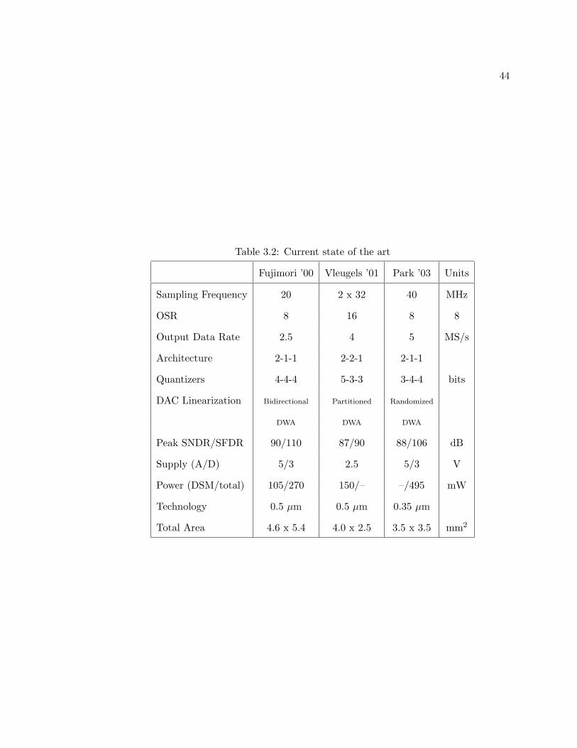
44
Table 3.2: Current state of the art
Fujimori ’00 Vleugels ’01 Park ’03 Units
Sampling Frequency 20 2 x 32 40 MHz
OSR 8 16 8 8
Output Data Rate 2.5 4 5 MS/s
Architecture 2-1-1 2-2-1 2-1-1
Quantizers 4-4-4 5-3-3 3-4-4 bits
DAC Linearization Bidirectional Partitioned Randomized
DWA DWA DWA
Peak SNDR/SFDR 90/110 87/90 88/106 dB
Supply (A/D) 5/3 2.5 5/3 V
Power (DSM/total) 105/270 150/– –/495 mW
Technology 0.5 µm 0.5 µm 0.35 µm
Total Area 4.6 x 5.4 4.0 x 2.5 3.5 x 3.5 mm2

45
CHAPTER 4. PROPOSED SOLUTIONS
This Chapter presents three techniques that deal with the problems described in
the previous Chapter.
4.1. Low-Distortion Delta-Sigma Topologies
As described in Section 3.1., distortion is caused by nonlinear opamp characteris-
tics. The signals processed by the opamps contain filtered versions of the input u, from
which they create harmonics. Inherent high-pass filtering functions in the modulator
attenuate these nonlinear effects, but not sufficiently for wideband signals.
One way to deal with the issue of opamp distortion is to prevent the opamps from
processing input signal. This can be achieved by making the modulator’s signal transfer
function STF equal to 1, allowing the input signal and quantization noise to be processed
separately [9, 10, 11]. Figure 4.1 shows a topology that can achieve this.
H(z)H(z) H(z)H(z) QQ
D/AD/Ab=1
c1=1
u
vc2=1
q1
a2=1
a1=2
yi1 yi2e
Figure 4.1: Low-distortion topology
Assuming that the structure coefficients have the values shown in the Figure, the
signal transfer function is given by

46
STF (z) =1 + 2H + H2
1 + 2H + H2= 1 (4.1)
where H(z) = z−1/(1 − z−1). The feedforward paths add the term 1 + 2H in the
numerator of the signal transfer function, making it equivalent to the denominator, and
therefore making STF = 1. The noise transfer function is the same as for a conventional
topology:
NTF (z) =1
1 + 2H + H2= (1− z−1)2 (4.2)
Therefore, the error signal e, at the input of the first integrator, is now given by
E(z) = U(z) · [1− STF (z)] + Q(z) ·NTF (z) = Q(z) ·NTF (z) (4.3)
indicating that the integrators process only quantization noise. Since no input signal is
processed by the integrators, no input signal harmonics can be generated. The integrator
nonlinearities will, however, still affect the quantization error, and may cause an increased
in-band noise floor. This can be avoided by reducing the output swing of the opamps,
with proper scaling of integrator coefficients. This process is now independent of the
input signal amplitude.
In practice, the cancellation of u and v will not be perfect. As indicated before, v
is an estimate of u, and its accuracy depends on the matching of electrical parameters.
Hence, there will be some residual signal component in e and at the outputs of the
integrators, but this will be normally negligible.
Figure 4.2 shows the simulated spectra of the low-distortion topology. The simu-
lation shown previously in Fig. 3.3, for the conventional topology, is repeated here for
comparison. The simulation conditions are the same as described in Section 3.1., for
Fig. 3.3. To keep the comparison fair, the coefficients in the low-distortion topology
were adjusted so that its integrator outputs have voltage swings similar to those of the
conventional topology, therefore using similar nonlinear ranges. However, the overall
transfer functions are equivalent.
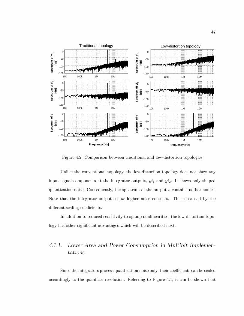
47
Frequency [Hz]
Traditional topology
Frequency [Hz]
Sp
ectr
um
of
v [d
B]
Sp
ectr
um
of
yi1
[dB
]S
pec
tru
m o
fyi
2
[dB
]
10k 100k 1M 10M
10k 100k 1M 10M
10k 100k 1M 10M
0
-50
-100
-150
0
-50
-100
-150
0
-50
-100
-150
Low-distortion topology
Sp
ectr
um
of
v [d
B]
Sp
ectr
um
of
yi1
[dB
]S
pec
tru
m o
fyi
2
[dB
]
10k 100k 1M 10M
10k 100k 1M 10M
10k 100k 1M 10M
0
-50
-100
-150
0
-50
-100
-150
0
-50
-100
-150
Figure 4.2: Comparison between traditional and low-distortion topologies
Unlike the conventional topology, the low-distortion topology does not show any
input signal components at the integrator outputs, yi1 and yi2. It shows only shaped
quantization noise. Consequently, the spectrum of the output v contains no harmonics.
Note that the integrator outputs show higher noise contents. This is caused by the
different scaling coefficients.
In addition to reduced sensitivity to opamp nonlinearities, the low-distortion topo-
logy has other significant advantages which will be described next.
4.1.1. Lower Area and Power Consumption in Multibit Implemen-tations
Since the integrators process quantization noise only, their coefficients can be scaled
accordingly to the quantizer resolution. Referring to Figure 4.1, it can be shown that
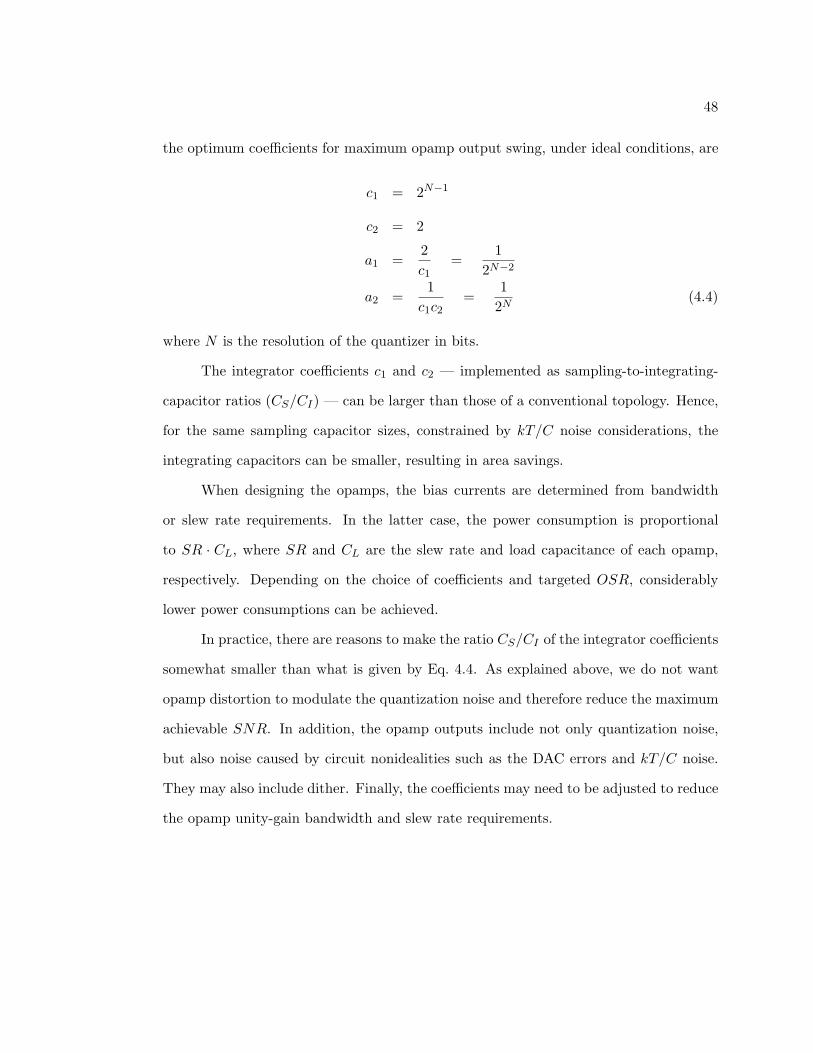
48
the optimum coefficients for maximum opamp output swing, under ideal conditions, are
c1 = 2N−1
c2 = 2
a1 =2c1
=1
2N−2
a2 =1
c1c2=
12N
(4.4)
where N is the resolution of the quantizer in bits.
The integrator coefficients c1 and c2 — implemented as sampling-to-integrating-
capacitor ratios (CS/CI) — can be larger than those of a conventional topology. Hence,
for the same sampling capacitor sizes, constrained by kT/C noise considerations, the
integrating capacitors can be smaller, resulting in area savings.
When designing the opamps, the bias currents are determined from bandwidth
or slew rate requirements. In the latter case, the power consumption is proportional
to SR · CL, where SR and CL are the slew rate and load capacitance of each opamp,
respectively. Depending on the choice of coefficients and targeted OSR, considerably
lower power consumptions can be achieved.
In practice, there are reasons to make the ratio CS/CI of the integrator coefficients
somewhat smaller than what is given by Eq. 4.4. As explained above, we do not want
opamp distortion to modulate the quantization noise and therefore reduce the maximum
achievable SNR. In addition, the opamp outputs include not only quantization noise,
but also noise caused by circuit nonidealities such as the DAC errors and kT/C noise.
They may also include dither. Finally, the coefficients may need to be adjusted to reduce
the opamp unity-gain bandwidth and slew rate requirements.

49
4.1.2. Improved Input Signal Range
The fact that no signal is processed by the integrators means that the output swing
of the opamps cannot limit the input signal amplitude. In fact, the only elements that
have to accommodate the full input signal swing are the switches and the quantizer.
In conventional topologies, care must be taken to ensure that the opamp outputs do
not saturate for maximum signal amplitude, which is accomplished by designing the
integrator coefficients for the worst case scenario. This is not necessary in the low-
distortion topology.
4.1.3. Only one DAC Needed in the Feedback Path
Most ∆Σ A/D modulator topologies use distributed feedback and require two
or more DACs for their implementation. Although not necessary for low-distortion
operation, the presented topology has only one DAC in the feedback loop, making it more
convenient for circuit implementation. For multibit DACs, the savings in terms of area
and complexity can be significant, especially if calibration is used for DAC linearization.
4.1.4. Simplified MASH Architecture
As it has been shown in previous examples, MASH architectures require coupling
of the quantization noise of one stage to another, and this usually requires subtracting
the quantizer output from its input. Extra analog circuitry is necessary to implement this
operation. The low distortion topology is especially useful for this application because
the quantization noise is directly available at the output of the second integrator, as
shown in Figure 4.3.
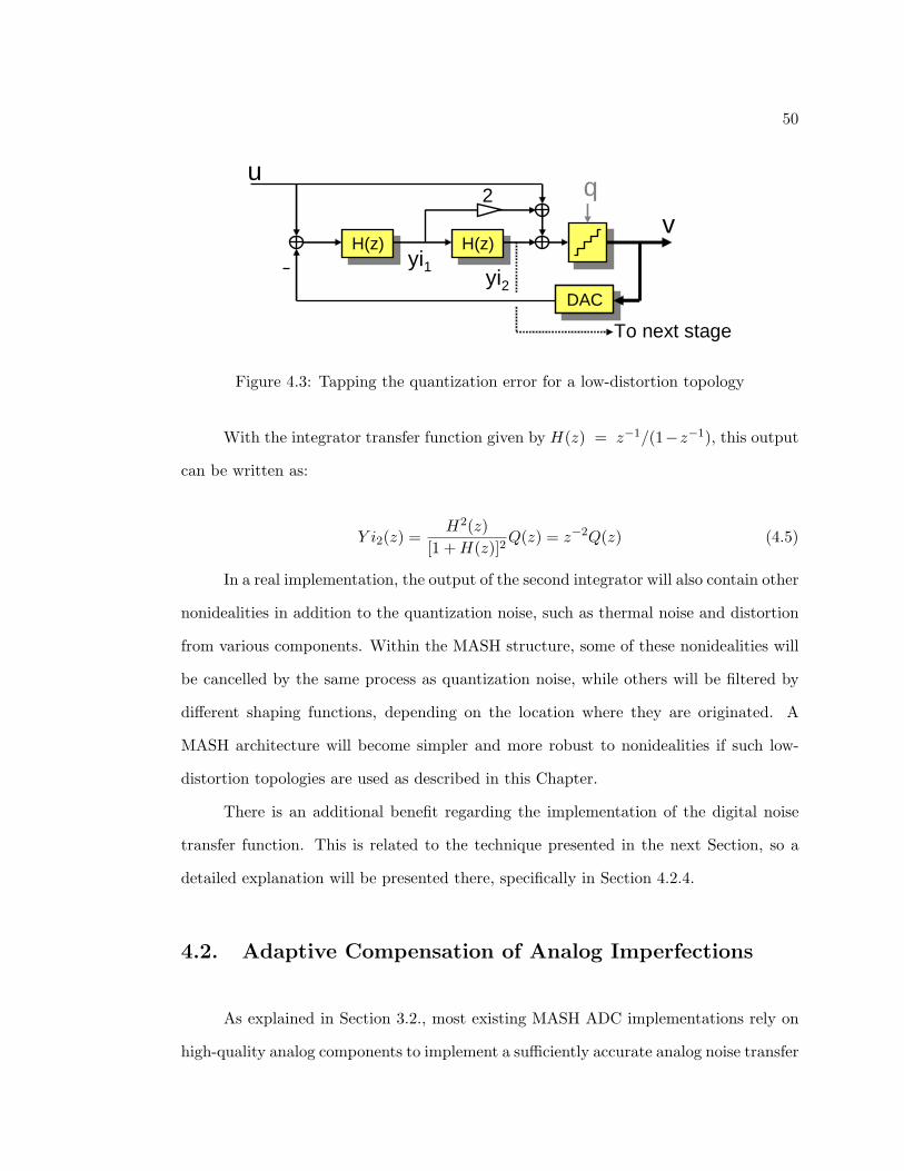
50
H(z)H(z) H(z)H(z)
u
vyi1
yi2
2
DACDAC
q
To next stage
Figure 4.3: Tapping the quantization error for a low-distortion topology
With the integrator transfer function given by H(z) = z−1/(1−z−1), this output
can be written as:
Y i2(z) =H2(z)
[1 + H(z)]2Q(z) = z−2Q(z) (4.5)
In a real implementation, the output of the second integrator will also contain other
nonidealities in addition to the quantization noise, such as thermal noise and distortion
from various components. Within the MASH structure, some of these nonidealities will
be cancelled by the same process as quantization noise, while others will be filtered by
different shaping functions, depending on the location where they are originated. A
MASH architecture will become simpler and more robust to nonidealities if such low-
distortion topologies are used as described in this Chapter.
There is an additional benefit regarding the implementation of the digital noise
transfer function. This is related to the technique presented in the next Section, so a
detailed explanation will be presented there, specifically in Section 4.2.4.
4.2. Adaptive Compensation of Analog Imperfections
As explained in Section 3.2., most existing MASH ADC implementations rely on
high-quality analog components to implement a sufficiently accurate analog noise transfer
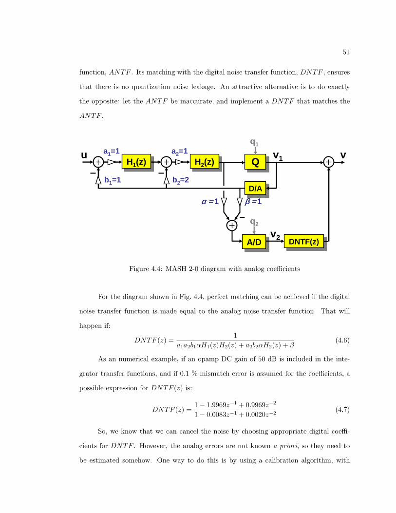
51
function, ANTF . Its matching with the digital noise transfer function, DNTF , ensures
that there is no quantization noise leakage. An attractive alternative is to do exactly
the opposite: let the ANTF be inaccurate, and implement a DNTF that matches the
ANTF .
H1(z)H1(z) H2(z)H2(z) QQ
D/AD/Ab1=1 b2=2
a1=1
A/DA/D DNTF(z)DNTF(z)
α = α = α = α = 1111 β = β = β = β = 1111
u vv1
v2
a2=1q1
q2
Figure 4.4: MASH 2-0 diagram with analog coefficients
For the diagram shown in Fig. 4.4, perfect matching can be achieved if the digital
noise transfer function is made equal to the analog noise transfer function. That will
happen if:
DNTF (z) =1
a1a2b1αH1(z)H2(z) + a2b2αH2(z) + β(4.6)
As an numerical example, if an opamp DC gain of 50 dB is included in the inte-
grator transfer functions, and if 0.1 % mismatch error is assumed for the coefficients, a
possible expression for DNTF (z) is:
DNTF (z) =1− 1.9969z−1 + 0.9969z−2
1− 0.0083z−1 + 0.0020z−2(4.7)
So, we know that we can cancel the noise by choosing appropriate digital coeffi-
cients for DNTF . However, the analog errors are not known a priori, so they need to
be estimated somehow. One way to do this is by using a calibration algorithm, with

52
the disadvantage of requiring the ADC to be unavailable during the estimation time. A
much more attractive way is to use adaptive noise cancellation, which can be used both
online or off-line.
4.2.1. Adaptive Noise Cancellation Basics
Adaptive noise cancellation is a well known and developed technique [35]. Some
examples of its applications are echo cancellation, system modeling, and adaptive channel
equalization. To understand how this technique can be useful, consider first the simplified
diagram of a noise cancellation system, shown in Figure 4.5.
correlatorcorrelator
kn
kk nu +ke
ky
ky
)(zF
)(ˆ zF
Figure 4.5: Adaptive filter basics
In this diagram, a desired signal uk is corrupted by the additive noise nk. This
is filtered by an unknown transfer function F (z), resulting in the noisy output signal
yk. If the noise nk, or a correlated version of it, is available independently of the signal
uk, then that can be used to remove the noise from the output yk. However, it must
first be filtered by a transfer function identical to F (z), denoted in the diagram as F (z).
Although F (z) is unknown, it can be estimated by correlating the noise nk with the error

53
signal ek, which is given by:
E(z) = Y (z)− Y (z) = [U(z) + N(z)] · F (z)−N(z) · F (z)
= U(z) · F (z) + N(z) · [F (z)− F (z)] (4.8)
The purpose of the correlator is to adapt the coefficients in F (z) until the noise
disappears from the error signal ek. When that happens, F (z) will be identical to F (z),
and the error signal will contain only U(z)·F (z). A cost function is used in the correlator
to ensure that the filter coefficients converge to the proper values. The whole process
can run in the background, since the correlator does not (ideally) take into account the
desired signal uk in its estimation of filter coefficients.
4.2.2. Adaptive Compensation of Quantization Noise Leakage
The concept described above can be readily applied to MASH ADC architectures.
The diagram in Figure 4.6 shows the back-end of the MASH 2-0 architecture described
previously. A pseudo-random test signal is introduced before the quantizer, so it follows
the same transfer functions as the quantization noise q1 [12, 13]. A correlator adapts
the coefficients of DNTF so that the test signal (and therefore q1) are minimized at the
output v. The test signal also works as dither, as described in Section 2.8.1.
It was shown in Eq. 4.7 that the optimum DNTF is a IIR filter. However, there
are some disadvantages in implementing this transfer function as an adaptive filter [36]:
• The filter can become unstable (its poles may move outside the unit circle).
• In general, an IIR adaptive filter does not have a unique minimum in its cost-
function. The solution found by the adaptive algorithm may not be the best one.
• The adaptation process cannot control the filter’s phase response and group delay.
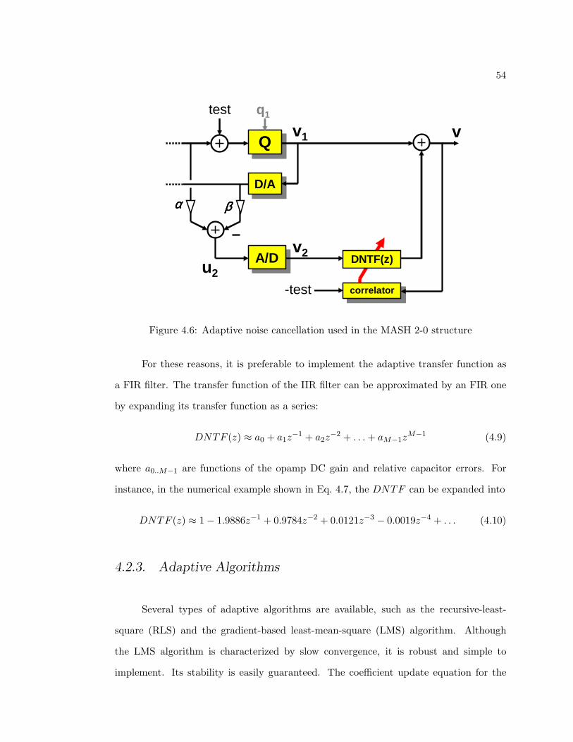
54
D/AD/A
A/DA/D
αααα ββββ
vv1
v2
q1test
correlatorcorrelator-test
DNTF(z)u2
Figure 4.6: Adaptive noise cancellation used in the MASH 2-0 structure
For these reasons, it is preferable to implement the adaptive transfer function as
a FIR filter. The transfer function of the IIR filter can be approximated by an FIR one
by expanding its transfer function as a series:
DNTF (z) ≈ a0 + a1z−1 + a2z
−2 + . . . + aM−1zM−1 (4.9)
where a0..M−1 are functions of the opamp DC gain and relative capacitor errors. For
instance, in the numerical example shown in Eq. 4.7, the DNTF can be expanded into
DNTF (z) ≈ 1− 1.9886z−1 + 0.9784z−2 + 0.0121z−3 − 0.0019z−4 + . . . (4.10)
4.2.3. Adaptive Algorithms
Several types of adaptive algorithms are available, such as the recursive-least-
square (RLS) and the gradient-based least-mean-square (LMS) algorithm. Although
the LMS algorithm is characterized by slow convergence, it is robust and simple to
implement. Its stability is easily guaranteed. The coefficient update equation for the
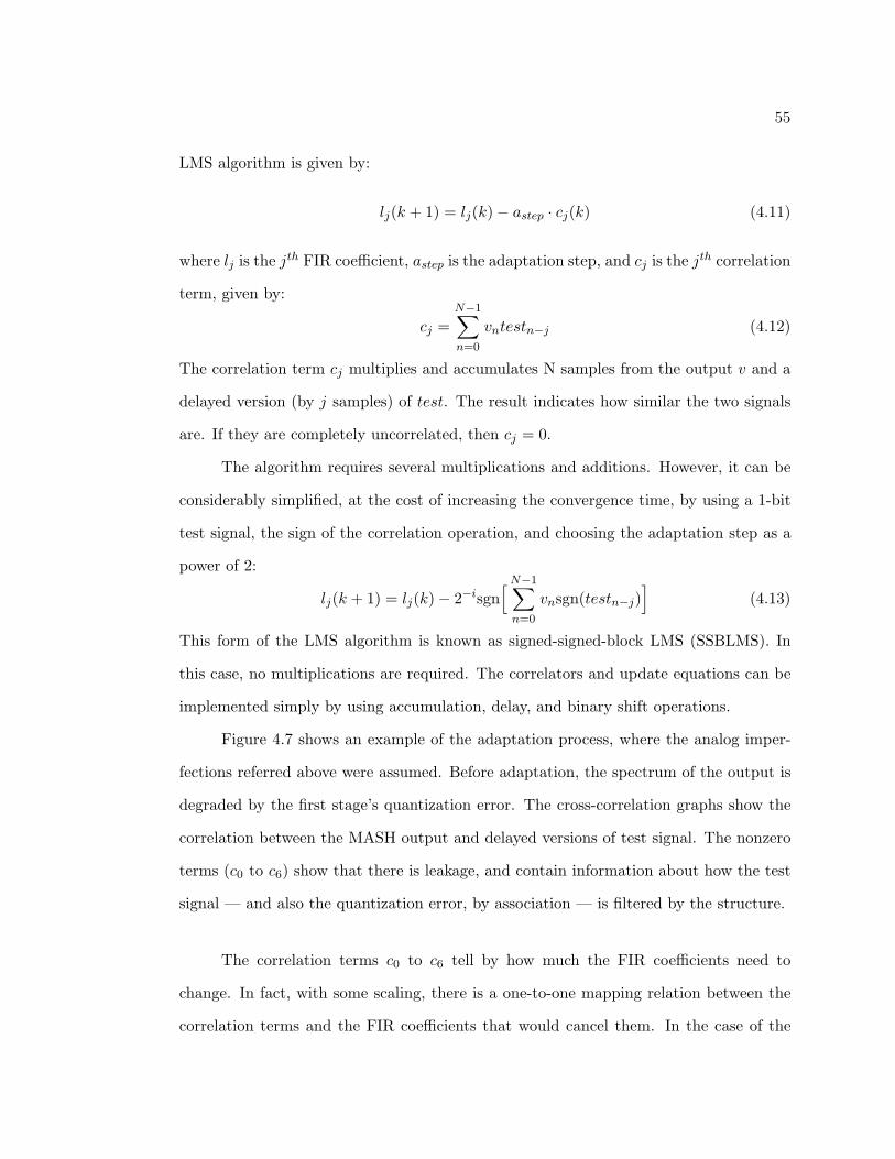
55
LMS algorithm is given by:
lj(k + 1) = lj(k)− astep · cj(k) (4.11)
where lj is the jth FIR coefficient, astep is the adaptation step, and cj is the jth correlation
term, given by:
cj =N−1∑
n=0
vntestn−j (4.12)
The correlation term cj multiplies and accumulates N samples from the output v and a
delayed version (by j samples) of test. The result indicates how similar the two signals
are. If they are completely uncorrelated, then cj = 0.
The algorithm requires several multiplications and additions. However, it can be
considerably simplified, at the cost of increasing the convergence time, by using a 1-bit
test signal, the sign of the correlation operation, and choosing the adaptation step as a
power of 2:
lj(k + 1) = lj(k)− 2−isgn[ N−1∑
n=0
vnsgn(testn−j)]
(4.13)
This form of the LMS algorithm is known as signed-signed-block LMS (SSBLMS). In
this case, no multiplications are required. The correlators and update equations can be
implemented simply by using accumulation, delay, and binary shift operations.
Figure 4.7 shows an example of the adaptation process, where the analog imper-
fections referred above were assumed. Before adaptation, the spectrum of the output is
degraded by the first stage’s quantization error. The cross-correlation graphs show the
correlation between the MASH output and delayed versions of test signal. The nonzero
terms (c0 to c6) show that there is leakage, and contain information about how the test
signal — and also the quantization error, by association — is filtered by the structure.
The correlation terms c0 to c6 tell by how much the FIR coefficients need to
change. In fact, with some scaling, there is a one-to-one mapping relation between the
correlation terms and the FIR coefficients that would cancel them. In the case of the
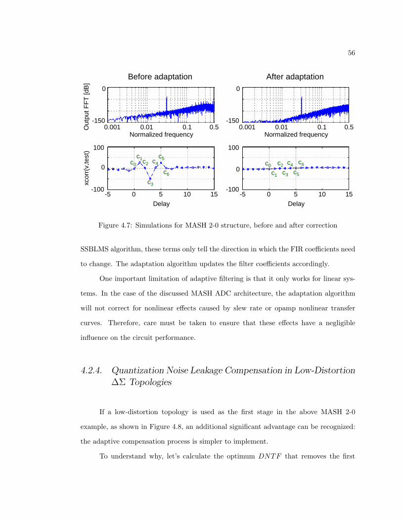
56
Before adaptation After adaptation
0 5 15-5 10 0 5 15-5 10
0
-150
0
-150
0
-100
100
0
-100
100
0.50.10.010.001 0.50.10.010.001
c0
c1c2
c3
c4
c5c0
c1
c2
c3
c4
c5c6
c6
DelayDelay
Normalized frequency Normalized frequency
Out
put F
FT
[dB
]xc
orr(
v,te
st)
Figure 4.7: Simulations for MASH 2-0 structure, before and after correction
SSBLMS algorithm, these terms only tell the direction in which the FIR coefficients need
to change. The adaptation algorithm updates the filter coefficients accordingly.
One important limitation of adaptive filtering is that it only works for linear sys-
tems. In the case of the discussed MASH ADC architecture, the adaptation algorithm
will not correct for nonlinear effects caused by slew rate or opamp nonlinear transfer
curves. Therefore, care must be taken to ensure that these effects have a negligible
influence on the circuit performance.
4.2.4. Quantization Noise Leakage Compensation in Low-Distortion∆Σ Topologies
If a low-distortion topology is used as the first stage in the above MASH 2-0
example, as shown in Figure 4.8, an additional significant advantage can be recognized:
the adaptive compensation process is simpler to implement.
To understand why, let’s calculate the optimum DNTF that removes the first
57
stage’s quantization error from the MASH ADC output. The output is given by:
V = V1 · z−2 + DNTF · V2 (4.14)
Note that there is now a z−2 block following the output of the first stage. Its purpose
will be explained later. The output of the first stage is given by:
V1 = U + ANTF ·Q1 (4.15)
where the analog noise transfer function is:
ANTF =1
1 + b[c1c2H1H2 + c1a1H1](4.16)
As mentioned above, the quantization error can now be tapped directly from the
output of the second integrator. However, what is tapped is not purely q1. Its value is
converted to digital format by the second ADC, appearing in v2 as:
H1(z)H1(z) H2(z)H2(z) QQ
D/AD/A
b=1
c1=1
A/DA/D DNTF(z)DNTF(z)
u
vv1
v2
c2=1
q1
u2
a2=1
a1=2
z-2z-2
q2
Figure 4.8: MASH 2-0 with low-distortion topology
V2 = U2 + Q2 = −c1c2H1H2 ·ANTF ·Q1 + Q2 (4.17)
These expressions are substituted in Eq 4.14, resulting in the MASH ADC output:
V = U · z−2 +[z−2 − c1c2H1H2DNTF
] ·ANTF ·Q1 + DNTF ·Q2 (4.18)

58
In the above Equation, the quantization error q1 will be eliminated if the term multiplying
it is equal to zero. This will happen if:
DNTF (z) =z−2
c1c2H1(z)H2(z)(4.19)
When finite-gain effects and coefficient errors are substituted in this Equation, it is found
that this is a simple FIR filter. The poles of the integrators H1 and H2 become zeros
for DNTF ; their zeros, for delaying integrators, are at z → ∞, so the DNTF has no
finite poles5. Therefore, no IIR to FIR approximation is needed, and only three taps are
required to represent accurately a second-order ANTF .
The purpose of the z−2 block following the output of the first stage, v1, can now
be explained: It matches the delays in Q1. If it was not there, the DNTF would not be
causal.
4.3. Digital Estimation and Correction of DAC Errors
As described in Section 3.3., many of the existing methods of DAC linearization
work well to improve the spurious-free dynamic range (SFDR), but the SNDR degra-
dations that they cause are becoming more significant as the bandwidth of operation in-
creases. For wideband operation, it is desirable to estimate and remove the DAC errors,
as existing analog and mixed-signal calibration methods do. However, these methods
require taking the ADC off-line, which is a downside.
Fortunately, a technique that can perform these tasks during normal ADC oper-
ation exists [15, 16, 17]. It uses digital correlation to estimate the DAC unit-element
errors, and therefore does not take into account other signals that are present during
normal ADC operation. Furthermore, this technique is fully digital, so it does not suffer
5Even if non-delaying integrators are used, their zeros are at z = 0, so they become poles at z = 0,which are just delays. The claim that DNTF is simply an FIR filter is still valid.

59
from the nonideal effects caused by the analog components required in analog/mixed-
signal calibration methods. The way this method works is described next.
Consider the M -element unit-element DAC model shown in Figure 4.9. Its analog
output can be modeled as the sum of all the active elements, selected by the input word
b. Each bit bi in the input word can take the value 0 or 1. Thus,
vout = VLSB ·M∑
i=1
bi(1 + ei) (4.20)
Each element has a nominal value of 1, and a relative error denoted by ei. At this time,
offset and gain errors are not considered.
1 + e1Mb
b1
1 + e2b2
•••
1 + eMbM
Σvout
VLSB
Figure 4.9: Unit-element DAC model
Now assume that the output vout can be converted back to digital format by an
ideal, high-accuracy ADC. Also assume, for simplicity, that only one of the unit elements
is active for each sample k, so that only one of the errors ei is present at the output
of the ADC at a time. If a cross-correlation operation is performed between the ADC
output v and each element bi, the result is:
corrbi, v =K−1∑
k=0
bi(k)v(k) =K−1∑
k=0
bi(k)[1 + ei] =K−1∑
k=0
bi(k) + ei
K−1∑
k=0
bi(k) (4.21)
The first term in this expression is the number of times, out of K samples, that the
element bi was used. The second term is the number of times that its corresponding
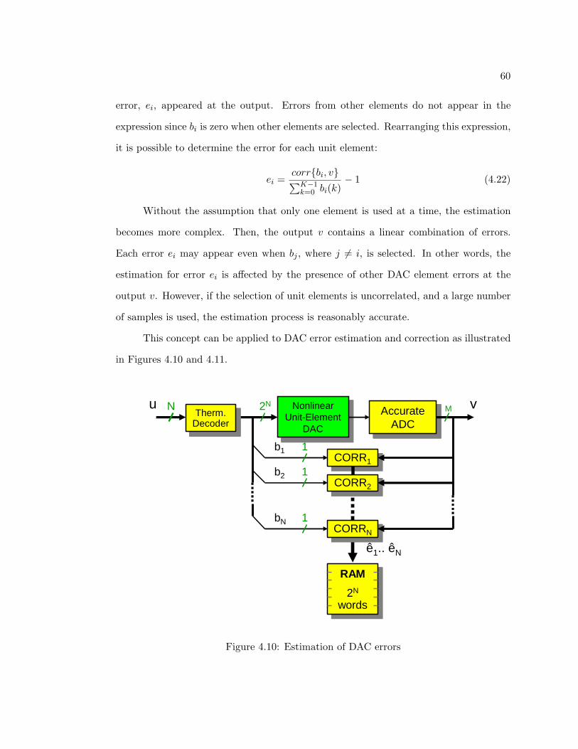
60
error, ei, appeared at the output. Errors from other elements do not appear in the
expression since bi is zero when other elements are selected. Rearranging this expression,
it is possible to determine the error for each unit element:
ei =corrbi, v∑K−1
k=0 bi(k)− 1 (4.22)
Without the assumption that only one element is used at a time, the estimation
becomes more complex. Then, the output v contains a linear combination of errors.
Each error ei may appear even when bj , where j 6= i, is selected. In other words, the
estimation for error ei is affected by the presence of other DAC element errors at the
output v. However, if the selection of unit elements is uncorrelated, and a large number
of samples is used, the estimation process is reasonably accurate.
This concept can be applied to DAC error estimation and correction as illustrated
in Figures 4.10 and 4.11.
Nonlinear Unit-Element
DAC
Nonlinear Unit-Element
DACAccurate
ADC
Accurate ADC
2N
CORR1CORR1
1b1
u vM
CORRNCORRN
1bN
CORR2CORR2
1b2
RAM
2N
words
RAM
2N
words
ê1.. êN
Therm. Decoder
Therm. Decoder
N
Figure 4.10: Estimation of DAC errors
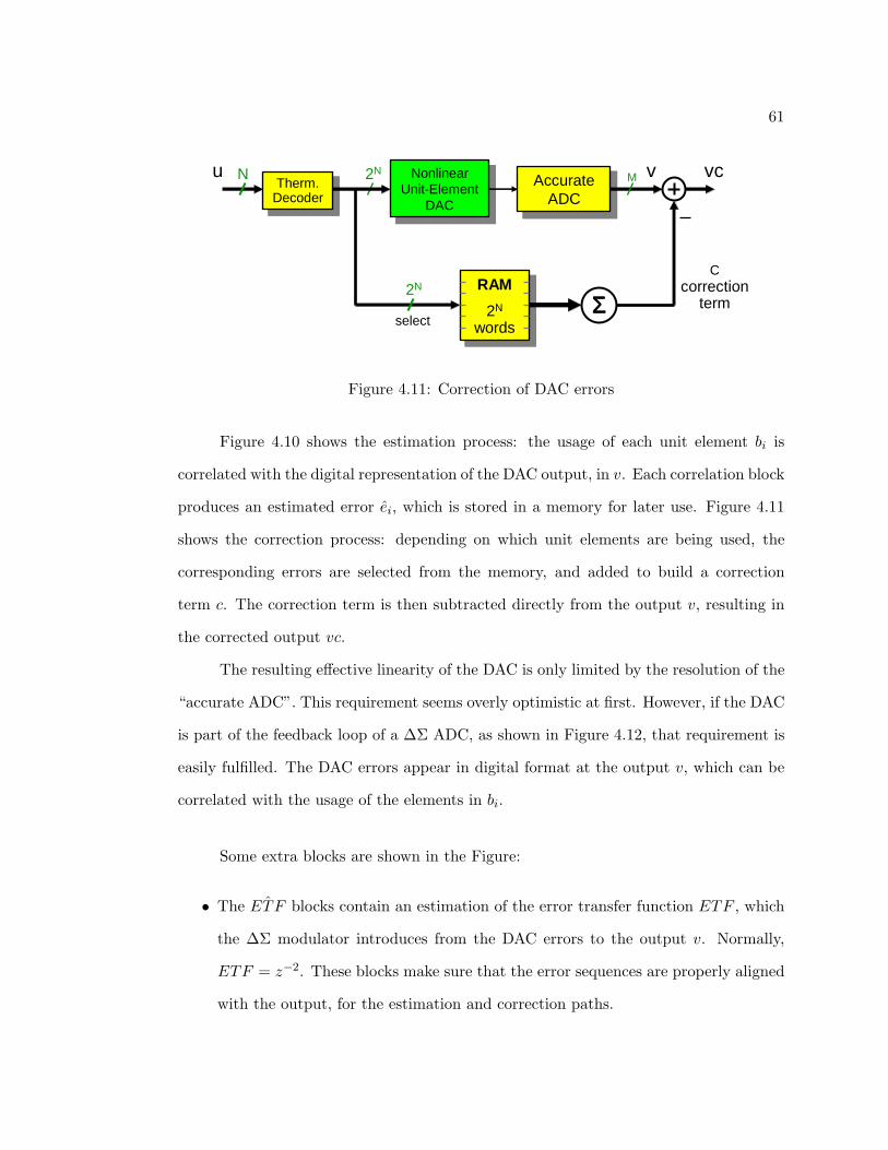
61
ΣΣΣΣ
vc
Ccorrection
term
Nonlinear Unit-Element
DAC
Nonlinear Unit-Element
DACAccurate
ADC
Accurate ADC
2N vM
RAM
2N
words
RAM
2N
words
2N
uTherm.
Decoder
Therm. Decoder
N
select
Figure 4.11: Correction of DAC errors
Figure 4.10 shows the estimation process: the usage of each unit element bi is
correlated with the digital representation of the DAC output, in v. Each correlation block
produces an estimated error ei, which is stored in a memory for later use. Figure 4.11
shows the correction process: depending on which unit elements are being used, the
corresponding errors are selected from the memory, and added to build a correction
term c. The correction term is then subtracted directly from the output v, resulting in
the corrected output vc.
The resulting effective linearity of the DAC is only limited by the resolution of the
“accurate ADC”. This requirement seems overly optimistic at first. However, if the DAC
is part of the feedback loop of a ∆Σ ADC, as shown in Figure 4.12, that requirement is
easily fulfilled. The DAC errors appear in digital format at the output v, which can be
correlated with the usage of the elements in bi.
Some extra blocks are shown in the Figure:
• The ˆETF blocks contain an estimation of the error transfer function ETF , which
the ∆Σ modulator introduces from the DAC errors to the output v. Normally,
ETF = z−2. These blocks make sure that the error sequences are properly aligned
with the output, for the estimation and correction paths.
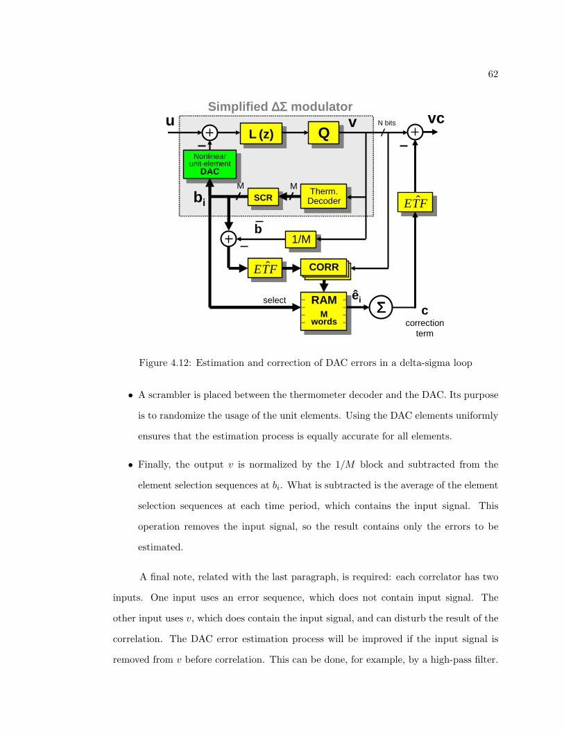
62
b i
M
L (z)L (z) QQ
Nonlinear unit-element
DAC
Nonlinear unit-element
DAC
u v N bits
Therm. Decoder
Therm. DecoderSCRSCR
M
ccorrection
term
êi
vc
FTE ˆ
FTE ˆ
b1/M1/M
Simplified ∆Σ∆Σ∆Σ∆Σ modulator
ΣΣΣΣRAMM
words
select
CORR
Figure 4.12: Estimation and correction of DAC errors in a delta-sigma loop
• A scrambler is placed between the thermometer decoder and the DAC. Its purpose
is to randomize the usage of the unit elements. Using the DAC elements uniformly
ensures that the estimation process is equally accurate for all elements.
• Finally, the output v is normalized by the 1/M block and subtracted from the
element selection sequences at bi. What is subtracted is the average of the element
selection sequences at each time period, which contains the input signal. This
operation removes the input signal, so the result contains only the errors to be
estimated.
A final note, related with the last paragraph, is required: each correlator has two
inputs. One input uses an error sequence, which does not contain input signal. The
other input uses v, which does contain the input signal, and can disturb the result of the
correlation. The DAC error estimation process will be improved if the input signal is
removed from v before correlation. This can be done, for example, by a high-pass filter.
63
CHAPTER 5. A HIGH-PERFORMANCE
DELTA-SIGMA ADC
The techniques described in the previous Chapter can be combined in a MASH
ADC architecture that can achieve and maintain high-resolution and wide-bandwidth
operation regardless of the performance of its analog components. A MASH ADC pro-
totype that makes full use of these techniques is described in this Chapter.
5.1. MASH 2-2-2 Architecture
To demonstrate the effectiveness of the presented techniques, it makes sense to
select a set of target specifications that fully explores their advantages:
• Low-distortion topologies allow the oversampling ratio to be minimized without
concerns about poor distortion suppression. The low value of OSR = 4 was se-
lected. A lower value than this would not be attractive since noise-shaping would
bring only scarce improvements to the resolution or even degrade it, as explained
previously regarding Figure 2.17.
• By using digital adaptive correction, the DC gain of the opamps is of reduced
concern. For a fixed gain-bandwidth product, the bandwidth can be maximized,
and simple, robust opamp topologies with good phase margin can be used. A
sampling frequency of 100 MHz was selected. In addition, since capacitor matching
is not a critical problem, the capacitors can be implemented with a simpler and
more compact layout.
• By using the fully-digital DAC error estimation and correction technique, it should
be possible to obtain a good resolution without worrying about how much noise
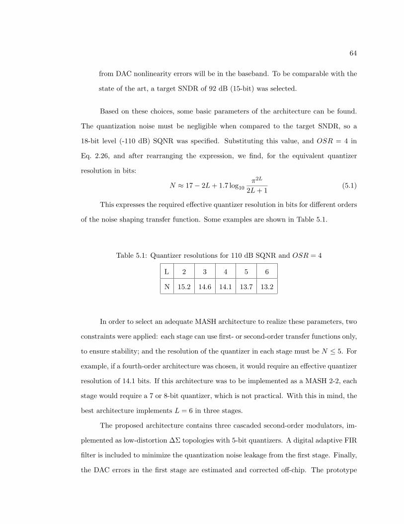
64
from DAC nonlinearity errors will be in the baseband. To be comparable with the
state of the art, a target SNDR of 92 dB (15-bit) was selected.
Based on these choices, some basic parameters of the architecture can be found.
The quantization noise must be negligible when compared to the target SNDR, so a
18-bit level (-110 dB) SQNR was specified. Substituting this value, and OSR = 4 in
Eq. 2.26, and after rearranging the expression, we find, for the equivalent quantizer
resolution in bits:
N ≈ 17− 2L + 1.7 log10
π2L
2L + 1(5.1)
This expresses the required effective quantizer resolution in bits for different orders
of the noise shaping transfer function. Some examples are shown in Table 5.1.
Table 5.1: Quantizer resolutions for 110 dB SQNR and OSR = 4
L 2 3 4 5 6
N 15.2 14.6 14.1 13.7 13.2
In order to select an adequate MASH architecture to realize these parameters, two
constraints were applied: each stage can use first- or second-order transfer functions only,
to ensure stability; and the resolution of the quantizer in each stage must be N ≤ 5. For
example, if a fourth-order architecture was chosen, it would require an effective quantizer
resolution of 14.1 bits. If this architecture was to be implemented as a MASH 2-2, each
stage would require a 7 or 8-bit quantizer, which is not practical. With this in mind, the
best architecture implements L = 6 in three stages.
The proposed architecture contains three cascaded second-order modulators, im-
plemented as low-distortion ∆Σ topologies with 5-bit quantizers. A digital adaptive FIR
filter is included to minimize the quantization noise leakage from the first stage. Finally,
the DAC errors in the first stage are estimated and corrected off-chip. The prototype
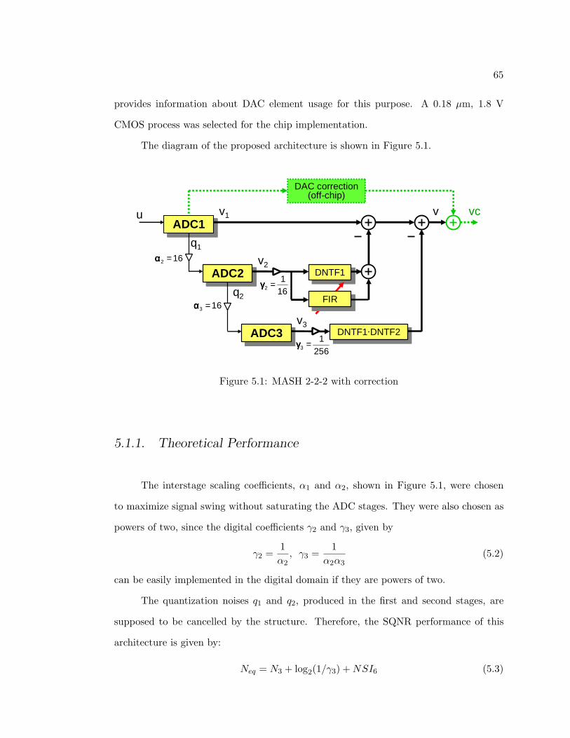
65
provides information about DAC element usage for this purpose. A 0.18 µm, 1.8 V
CMOS process was selected for the chip implementation.
The diagram of the proposed architecture is shown in Figure 5.1.
ADC1ADC1u v1
ADC2ADC2 DNTF1DNTF1v2
ADC3ADC3 DNTF1·DNTF2DNTF1·DNTF2v3
q1
q2
v
FIRFIR161
2 =γγγγ
2561
3 =γγγγ
162 =αααα
163 =αααα
DAC correction (off-chip)
vc
Figure 5.1: MASH 2-2-2 with correction
5.1.1. Theoretical Performance
The interstage scaling coefficients, α1 and α2, shown in Figure 5.1, were chosen
to maximize signal swing without saturating the ADC stages. They were also chosen as
powers of two, since the digital coefficients γ2 and γ3, given by
γ2 =1α2
, γ3 =1
α2α3(5.2)
can be easily implemented in the digital domain if they are powers of two.
The quantization noises q1 and q2, produced in the first and second stages, are
supposed to be cancelled by the structure. Therefore, the SQNR performance of this
architecture is given by:
Neq = N3 + log2(1/γ3) + NSI6 (5.3)
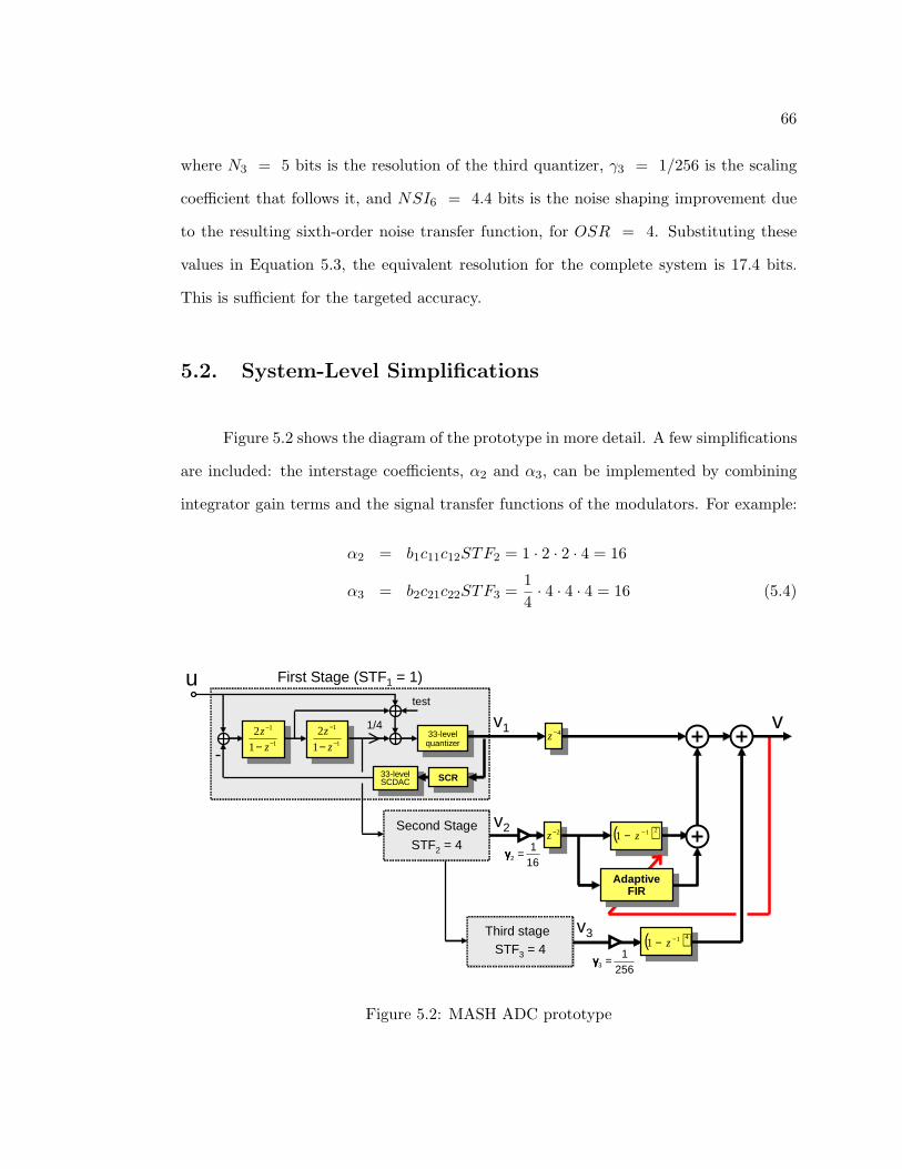
66
where N3 = 5 bits is the resolution of the third quantizer, γ3 = 1/256 is the scaling
coefficient that follows it, and NSI6 = 4.4 bits is the noise shaping improvement due
to the resulting sixth-order noise transfer function, for OSR = 4. Substituting these
values in Equation 5.3, the equivalent resolution for the complete system is 17.4 bits.
This is sufficient for the targeted accuracy.
5.2. System-Level Simplifications
Figure 5.2 shows the diagram of the prototype in more detail. A few simplifications
are included: the interstage coefficients, α2 and α3, can be implemented by combining
integrator gain terms and the signal transfer functions of the modulators. For example:
α2 = b1c11c12STF2 = 1 · 2 · 2 · 4 = 16
α3 = b2c21c22STF3 =14· 4 · 4 · 4 = 16 (5.4)
u
1
1
1
2−
−
− z
z1
1
1
2−
−
− z
z
test
( )211 −− z
First Stage (STF1 = 1)
Second Stage
1/4
Adaptive FIR
Adaptive FIR
4−z
( )411 −− z
33-level SCDAC
33-level SCDAC SCR
SCR
2−zSTF2 = 4
vv1
v2
v3Third stageSTF3 = 4
161
2 =γγγγ
2561
3 =γγγγ
33-level quantizer
33-level quantizer
Figure 5.2: MASH ADC prototype
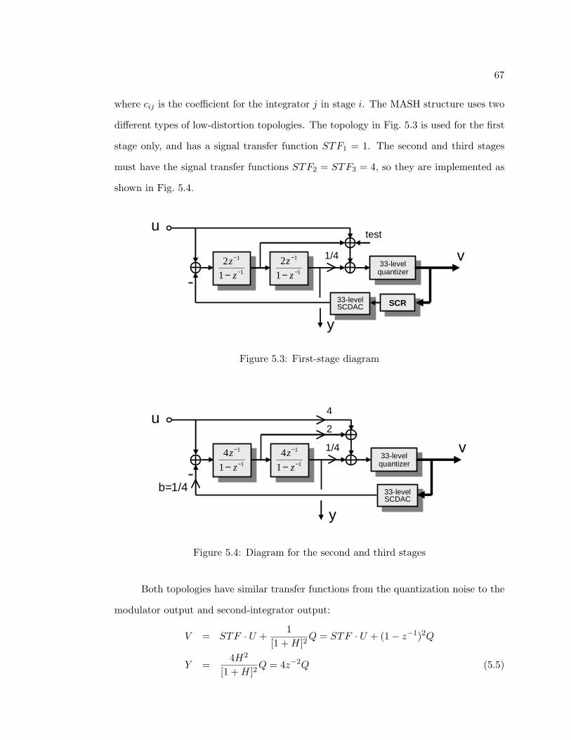
67
where cij is the coefficient for the integrator j in stage i. The MASH structure uses two
different types of low-distortion topologies. The topology in Fig. 5.3 is used for the first
stage only, and has a signal transfer function STF1 = 1. The second and third stages
must have the signal transfer functions STF2 = STF3 = 4, so they are implemented as
shown in Fig. 5.4.
u
33-level quantizer
33-level quantizer1
1
12
−
−
− z
z1
1
1
2−
−
− z
z
test
1/4
33-level SCDAC
33-level SCDAC SCR
SCR
v
y
Figure 5.3: First-stage diagram
u
33-level quantizer
33-level quantizer1
1
1
4−
−
− z
z1
1
1
4−
−
− z
z 1/4
33-level SCDAC
33-level SCDAC
v
y
2
4
1/4b=
Figure 5.4: Diagram for the second and third stages
Both topologies have similar transfer functions from the quantization noise to the
modulator output and second-integrator output:
V = STF · U +1
[1 + H]2Q = STF · U + (1− z−1)2Q
Y =4H2
[1 + H]2Q = 4z−2Q (5.5)
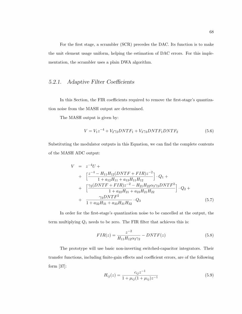
68
For the first stage, a scrambler (SCR) precedes the DAC. Its function is to make
the unit element usage uniform, helping the estimation of DAC errors. For this imple-
mentation, the scrambler uses a plain DWA algorithm.
5.2.1. Adaptive Filter Coefficients
In this Section, the FIR coefficients required to remove the first-stage’s quantiza-
tion noise from the MASH output are determined.
The MASH output is given by:
V = V1z−4 + V2γ2DNTF1 + V3γ3DNTF1DNTF2 (5.6)
Substituting the modulator outputs in this Equation, we can find the complete contents
of the MASH ADC output:
V = z−4U +
+[z−4 −H11H12(DNTF + FIR)z−2
1 + a12H11 + a13H11H12
]·Q1 +
+[γ2(DNTF + FIR)z−2 −H21H22α3γ3DNTF 2
1 + a22H21 + a23H21H22
]·Q2 +
+γ3DNTF 2
1 + a32H31 + a33H31H32·Q3 (5.7)
In order for the first-stage’s quantization noise to be cancelled at the output, the
term multiplying Q1 needs to be zero. The FIR filter that achieves this is:
FIR(z) =z−2
H11H12α2γ2−DNTF (z) (5.8)
The prototype will use basic non-inverting switched-capacitor integrators. Their
transfer functions, including finite-gain effects and coefficient errors, are of the following
form [37]:
Hij(z) =cijz
−1
1 + µij(1 + µij)z−1(5.9)

69
These integrator equations, and DNTF (z) = (1− z−1)2, can be substituted in the FIR
filter expression. This is given by FIR = l0 + l1z−1 + l2z
−2, with the filter coefficients
l0 to l2 determined as:
l0 =1 + µ11(1 + c11) + µ12(1 + c12) + µ11µ12(1 + c11 + c12 + c11c12)
c11c12α2α2− 1
l1 =2 + µ11(2 + c11 + µ12(2 + c12) + µ11µ12(2 + c11 + c12)
c11c12α2α2− 2
l2 =1 + µ11 + µ12 + µ11µ12
c11c12α2α2− 1 (5.10)
These expressions show that it is possible to correct for finite opamp gain (µ), integrator
gain (c) and interstage coefficient (α) errors. It also shows that the internal coefficients
of the modulators (aij) are irrelevant to the noise cancellation.
As a numerical example, if all opamps have a DC gain of 50 dB (µ = 3.16×10⁻³),
and everything else is ideal, then the FIR filter function is given by:
FIR(z) = 0.01906− 0.02536z−2 + 0.00633z−2 (5.11)
5.2.2. System Level Simulations
The proposed MASH architecture was simulated at system level using MATLAB R©
and Simulink R©. The simulations included nonidealities such as kT/C noise, quantizer
and DAC nonlinearities, and nonlinear opamp DC transfer curves. The values used in the
simulations for DAC linearity, quantizer linearity, and capacitor sizes were determined
as described in the next Chapter.
Figure 5.5 shows the spectrum of the MASH ADC output v, after adaptive filter
correction and DAC correction. The targeted SNDR of 92.4 dB can be calculated from
this spectrum.
It also shows the probability density functions of the input signals for all stages.
Note that these Figures include quantization noise, kT/C noise, and also modulated
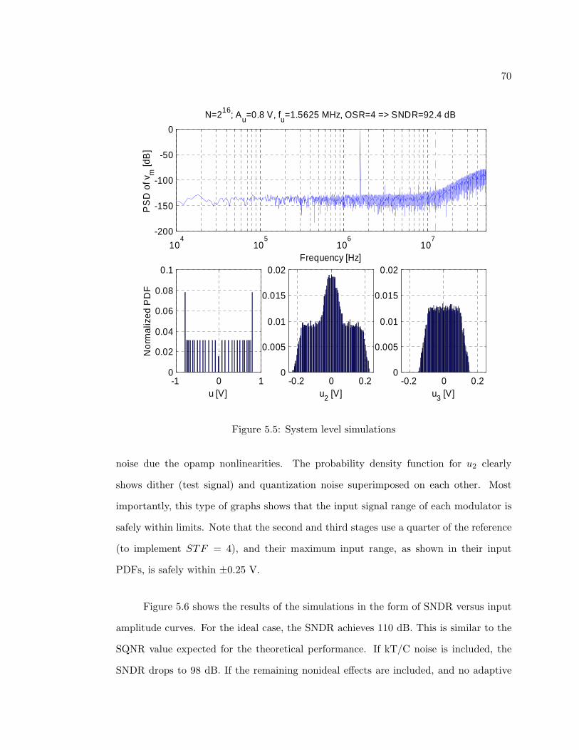
70
104
105
106
107
-200
-150
-100
-50
0
PS
D o
f vm
[dB
]
Frequency [Hz]
N=216; Au=0.8 V, fu=1.5625 MHz, OSR=4 => SNDR=92.4 dB
-1 0 10
0.02
0.04
0.06
0.08
0.1
u [V]
Nor
mal
ized
PD
F
-0.2 0 0.20
0.005
0.01
0.015
0.02
u2 [V]-0.2 0 0.2
0
0.005
0.01
0.015
0.02
u3 [V]
Figure 5.5: System level simulations
noise due the opamp nonlinearities. The probability density function for u2 clearly
shows dither (test signal) and quantization noise superimposed on each other. Most
importantly, this type of graphs shows that the input signal range of each modulator is
safely within limits. Note that the second and third stages use a quarter of the reference
(to implement STF = 4), and their maximum input range, as shown in their input
PDFs, is safely within ±0.25 V.
Figure 5.6 shows the results of the simulations in the form of SNDR versus input
amplitude curves. For the ideal case, the SNDR achieves 110 dB. This is similar to the
SQNR value expected for the theoretical performance. If kT/C noise is included, the
SNDR drops to 98 dB. If the remaining nonideal effects are included, and no adaptive
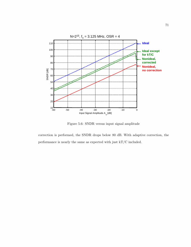
71
-60 -50 -40 -30 -20 -10 010
20
30
40
50
60
70
80
90
100
110
Input Signal Amplitude Au
[dB]
SN
DR
[dB
]
Nonideal,corrected
Ideal
Ideal exceptfor kT/C
Nonideal, no correction
N=215, fu = 3.125 MHz, OSR = 4
Figure 5.6: SNDR versus input signal amplitude
correction is performed, the SNDR drops below 80 dB. With adaptive correction, the
performance is nearly the same as expected with just kT/C included.
72
CHAPTER 6. NOISE AND LINEARITY
REQUIREMENTS
This Chapter describes how to analyze noise in the proposed MASH 2-2-2 archi-
tecture. Also, some key circuit parameters, such as capacitor sizes, and quantizer and
DAC linearity, are calculated based on the noise requirements.
6.1. Noise Analysis
The prototype was designed for 15-bit noise performance, corresponding to a target
SNDR of 92.1 dB. The maximum SNDR of the system is given by:
SNDRMAX =σ2
uMAX
σ2n
(6.1)
where σ2uMAX
is the maximum input signal power and σ2n is the total noise power, which
includes contributions from several noise sources:
σ2n = σ2
q + σ2nkT/C
+ σ2nOPAMP
+ σ2nDAC
+ σ2nOTHER
(6.2)
In this equation, the noise power terms refer to quantization, switch, opamp, DAC and
other noise sources, respectively. The latter term takes into account digital crosstalk and
other extrinsic effects.
The maximum undistorted input signal power, σ2uMAX
, is for a -2 dB input (0 dB
corresponds to the full-scale signal range, for an input signal amplitude Au = VREF /2).
This was determined from system level simulations.
σ2uMAX
=A2
uMAX
2=
(0.4VREF )2
2= 0.08V 2
REF (6.3)
For a reference voltage of VREF = 1.8 V, the maximum input signal power corresponds
73
to σ2uMAX
= 0.2592 V2rms, or -5.9 dBV. The total noise power for 15-bit performance is
then given by
σ2ndB = σ2
uMAXdB − SNDRdB15−bit= −5.9− 92.1 = −98.0 dBV (6.4)
which corresponds to σ2n = 161.3 (µVrms)2.
One of the terms in the total noise power is the quantization noise. This can be
determined from the maximum SQNR, which was obtained from system-level simulations
with no other noise sources included. The quantization noise power is given by:
σ2qdB = σ2
uMAXdB − SQNRdBMAX= −5.9− 109.0 = −114.9 dBV (6.5)
which corresponds to σ2q = 3.3 (µVrms)2. As expected, this value should be negligible
when compared with the total allowed noise power for 15-bit performance.
The noise contributed by the remaining sources will be calculated next.
6.2. Noise Sources
Figure 6.1 shows the simplified schematic of a low-distortion ∆Σ modulator, with
the most significant noise sources identified in the Figure. The noise associated with
switch thermal noise (kT/C) is represented by a source in series with each capacitor. The
noise generated in opamp devices, which includes thermal and flicker noise, is represented
by a source at the non-inverting input of each opamp.
All these noise sources can be combined into a simpler equivalent representation,
shown in Figure 6.2. In the Figure, vn1 and vn2 represent the switch and opamp noise
in the first and second integrators, respectively. The noise source vn3 represents the
combined switch noise from all the feedforward paths in the passive adder preceding the
quantizer.
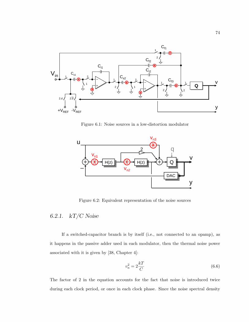
74
Vin 21
1
1
Ci1
Cs1Cs2
2 1
2
Ci2
1
2
Cf3
2
1
Cf2
Cf1
2
1
y
2.d 2.d
+VREF -VREF
v
Figure 6.1: Noise sources in a low-distortion modulator
H(z)H(z) H(z)H(z)
u
v2
DACDAC
q
Q
vn1
vn2
vn3
y
Figure 6.2: Equivalent representation of the noise sources
6.2.1. kT/C Noise
If a switched-capacitor branch is by itself (i.e., not connected to an opamp), as
it happens in the passive adder used in each modulator, then the thermal noise power
associated with it is given by [38, Chapter 4]:
v2n = 2
kT
C(6.6)
The factor of 2 in the equation accounts for the fact that noise is introduced twice
during each clock period, or once in each clock phase. Since the noise spectral density

75
of kT/C noise is flat, it can be calculated by dividing the power by the full bandwidth
of operation. It is therefore given by
Svn(f) =2fs
kT
C(6.7)
for single-sided PSD.
For the passive adder, the noise contributed by the three switched capacitor
branches can be represented by a single equivalent noise source, shown as vn3 in Fi-
gure 6.2. Its power is given by
v2n3 =
q2f1 + q2
f2 + q2f3
C2f1
=2kT
Cf1
[1 +
Cf2
Cf1+
Cf3
Cf1
](6.8)
If the switched capacitor branch is part of an integrator, its noise power is slightly
lower [39]. During one of the clock phases, one of capacitor plates is connected to the
input of an opamp, which introduces its own bandwidth limitations. Therefore, the noise
power is given by
v2n =
kT
C
2x + 1x + 1
(6.9)
where x = 2gmron includes the reduction effect caused by the finite bandwidth of the
opamp. In this parameter, gm is the effective transconductance of the opamp, and ron
is the on-resistance of the switches in the input branch, during the integration phase. If
the opamp has infinite bandwidth (meaning that gm → ∞), then x → ∞, and Eq. 6.9
tends to 2kT/C. If the settling times of the opamp and switched capacitor branch are
equal, then x = 2, and
v2n =
53
kT
C. (6.10)
6.2.2. Opamp Noise
The most important types of opamp noise are thermal and flicker noise. As shown
in Figure 6.3, thermal noise is flat over the opamp closed-loop bandwidth, while flicker
noise is concentrated at low frequencies.

76
f
Opamp Output Noise Spectral
Density
[V2/Hz]
FlickerThermal
Opamp Closed-Loop Bandwidth
Figure 6.3: Opamp noise spectrum
Due to the wideband nature of this project, thermal noise power dominates over
flicker noise power. Noise simulations performed for a typical integrator show that the
flicker noise contributes less than 10% of the total opamp noise power. Therefore, only
thermal noise will be considered in the following analysis. In applications where flicker
noise is significant, it can be reduced or suppressed by techniques such as correlated
double sampling or chopper stabilization [40].
The opamp thermal noise can be described by two noise sources [39]. One at its
input, modeled by
v2niOP
=43
kT
CS
11 + x
(6.11)
and another at its output, modeled by
v2noOP
=43
kT
CL(6.12)
where CL is the effective load capacitance of the opamp. Since the spectral density of
the input noise source is shaped by the integrator transfer function, its output referred
power is much larger than that of the output noise source. Therefore, only the input
noise source will be considered in subsequent calculations.
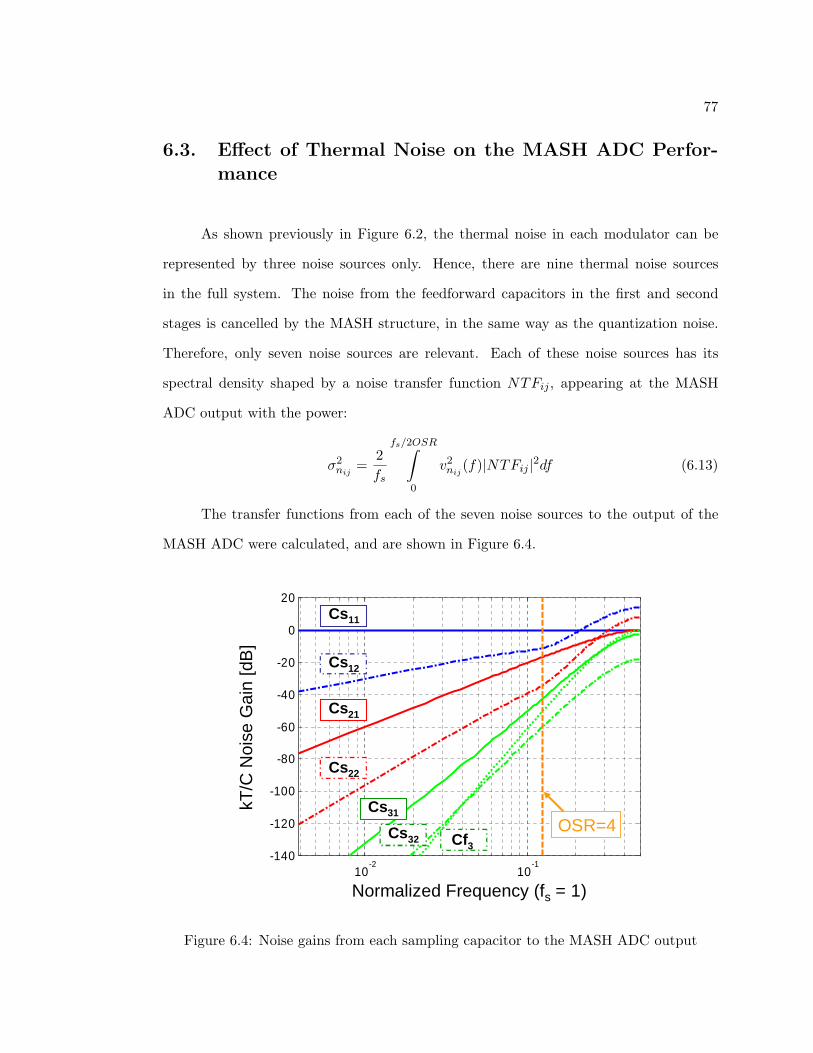
77
6.3. Effect of Thermal Noise on the MASH ADC Perfor-mance
As shown previously in Figure 6.2, the thermal noise in each modulator can be
represented by three noise sources only. Hence, there are nine thermal noise sources
in the full system. The noise from the feedforward capacitors in the first and second
stages is cancelled by the MASH structure, in the same way as the quantization noise.
Therefore, only seven noise sources are relevant. Each of these noise sources has its
spectral density shaped by a noise transfer function NTFij , appearing at the MASH
ADC output with the power:
σ2nij
=2fs
fs/2OSR∫
0
v2nij
(f)|NTFij |2df (6.13)
The transfer functions from each of the seven noise sources to the output of the
MASH ADC were calculated, and are shown in Figure 6.4.
10-2
10-1
-140
-120
-100
-80
-60
-40
-20
0
20
OSR=4
Cs11
Cs12
Cs21
Cs31
Cs32
Cs22
Normalized Frequency (fs = 1)
kT/C
Noi
se G
ain
[dB
]
Cf3
Figure 6.4: Noise gains from each sampling capacitor to the MASH ADC output
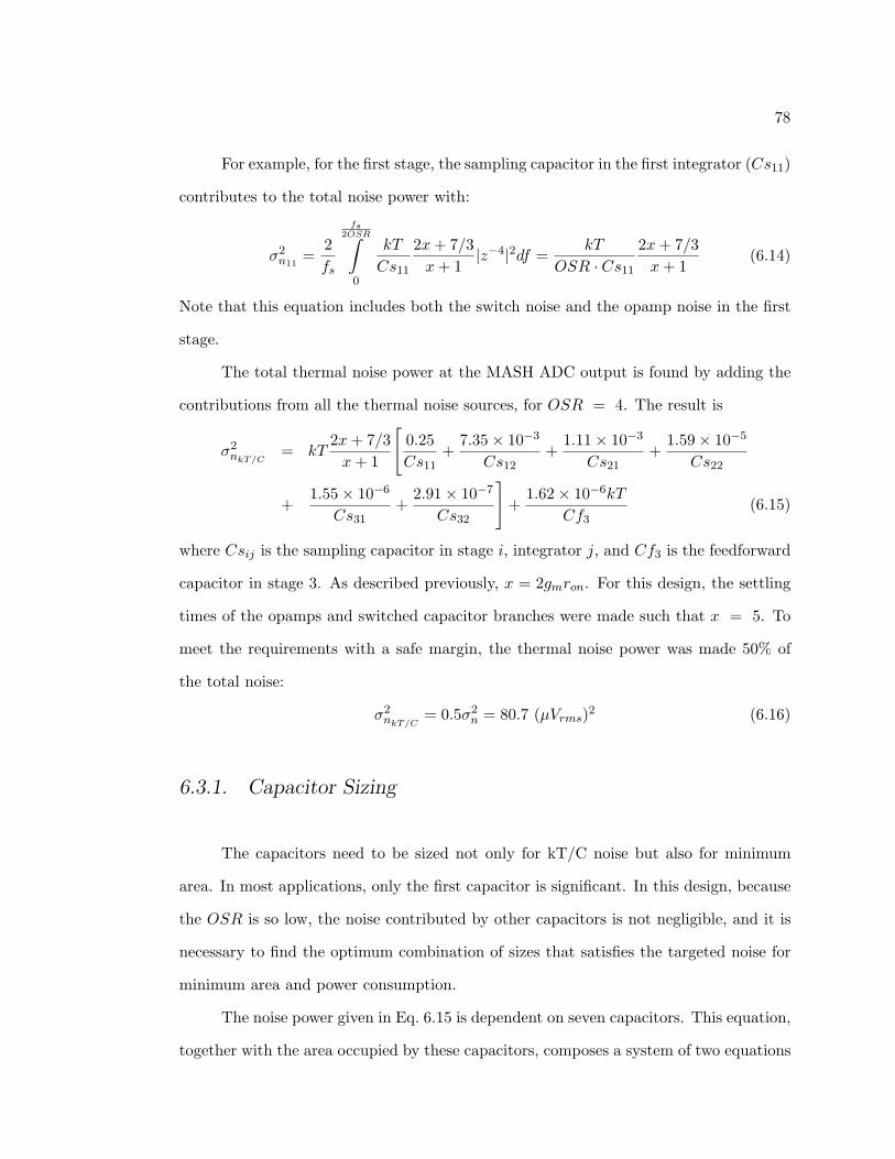
78
For example, for the first stage, the sampling capacitor in the first integrator (Cs11)
contributes to the total noise power with:
σ2n11
=2fs
fs2OSR∫
0
kT
Cs11
2x + 7/3x + 1
|z−4|2df =kT
OSR · Cs11
2x + 7/3x + 1
(6.14)
Note that this equation includes both the switch noise and the opamp noise in the first
stage.
The total thermal noise power at the MASH ADC output is found by adding the
contributions from all the thermal noise sources, for OSR = 4. The result is
σ2nkT/C
= kT2x + 7/3
x + 1
[0.25Cs11
+7.35× 10⁻³
Cs12+
1.11× 10⁻³
Cs21+
1.59× 10⁻⁵
Cs22
+1.55× 10⁻⁶
Cs31+
2.91× 10⁻⁷
Cs32
]+
1.62× 10⁻⁶kT
Cf3(6.15)
where Csij is the sampling capacitor in stage i, integrator j, and Cf3 is the feedforward
capacitor in stage 3. As described previously, x = 2gmron. For this design, the settling
times of the opamps and switched capacitor branches were made such that x = 5. To
meet the requirements with a safe margin, the thermal noise power was made 50% of
the total noise:
σ2nkT/C
= 0.5σ2n = 80.7 (µVrms)2 (6.16)
6.3.1. Capacitor Sizing
The capacitors need to be sized not only for kT/C noise but also for minimum
area. In most applications, only the first capacitor is significant. In this design, because
the OSR is so low, the noise contributed by other capacitors is not negligible, and it is
necessary to find the optimum combination of sizes that satisfies the targeted noise for
minimum area and power consumption.
The noise power given in Eq. 6.15 is dependent on seven capacitors. This equation,
together with the area occupied by these capacitors, composes a system of two equations
79
with seven unknowns. To solve these equations, a linear programming method, such
as convex optimization, would be required. Fortunately, in this case, only the first and
second capacitors are dominant, so we have only two variables to determine, giving the
system a closed-form solution. The two equations are:
σ2nkT/C
≈ kT[
N11Cs11
+ N12Cs12
]
∂CTOTAL∂Cs11
= 0(6.17)
where N11 and N12 are the noise factors associated with Cs11 and Cs12, respectively.
Their values are given by:
N11 =2x + 7/3
x + 1· 0.25 N12 =
2x + 7/3x + 1
· 7.35× 10−3 (6.18)
There are two sets of solutions to this system of equations, but only one is valid:
Cs11 = kTN11 +
√N11N12
σ2nkT/C
and Cs12 =kTN12Cs11
σ2nkT/C
Cs11 − kTN11(6.19)
This solution is plotted in Figure 6.5, together with the relation between the two
capacitors for the required noise performance. The choice of capacitors for implementa-
tion is Cs11 = 32 pF and Cs12 = 6 pF. These unusually large values are required due
to the high SNR and low OSR specifications. The remaining capacitor values in the
system were chosen for matching and other properties, rather than for their kT/C and
opamp noise contributions.
6.4. Quantizer Linearity
In general, quantizer linearity is not critical. The quantizer errors in the first and
second stages are cancelled by normal MASH operation, as it happens for the quantiza-
tion noise. For the third stage, the quantizer errors are shaped by a sixth-order noise
transfer function. However, there are reasons to limit the nonlinearities in the quantizers.

80
30 32 34 36 38 40
3
4
5
6
7
8
Cs11
[pF]
Cs 12
[pF
]
Capacitance relation for σkT/C2 =80.7 (µV)2
Cs11
=30.92 pF, Cs12
=5.3 pF
Figure 6.5: Relation between Cs11 and Cs12 for the targeted noise
• They add to the quantization noise power, reducing the dynamic range for each
stage. In fact, the output swing of the opamps in all stages is used up by quantiza-
tion noise, kT/C and opamp noise, by DAC nonlinearity errors, and by quantizer
nonlinearity errors. In addition, for the first stage, there needs to be extra room
for the test signal used by the adaptive algorithm.
• If the nonlinearity errors are larger than the quantizer’s resolution, then the quan-
tizer operation is not monotonic, causing problems in the operation of the ∆Σ
modulator. However, this is unlikely to happen for such low-resolution (5-bit)
quantizers.
Due to these considerations, the quantizers were designed for a target linearity of
7 bits. This means that, instead of having quantization errors within ±VLSB/2 (corre-
sponding to infinite linearity), they are allowed to be as large as ±(VLSB/2+VLSB/8), or
±5VLSB/8. The quantizer circuit design is described in the next Chapter, in Section 7.4.
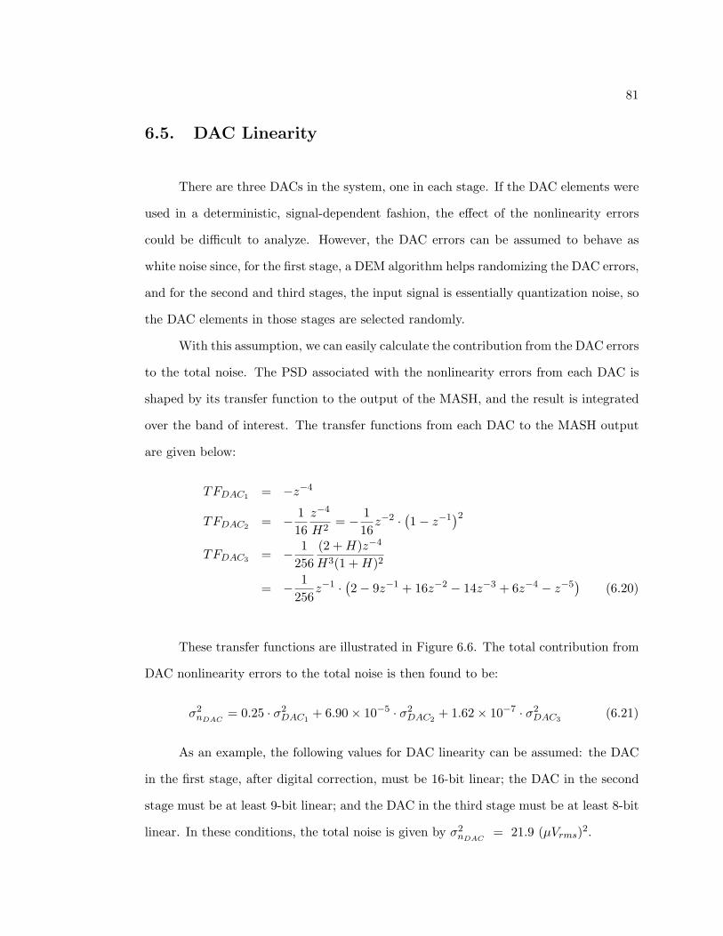
81
6.5. DAC Linearity
There are three DACs in the system, one in each stage. If the DAC elements were
used in a deterministic, signal-dependent fashion, the effect of the nonlinearity errors
could be difficult to analyze. However, the DAC errors can be assumed to behave as
white noise since, for the first stage, a DEM algorithm helps randomizing the DAC errors,
and for the second and third stages, the input signal is essentially quantization noise, so
the DAC elements in those stages are selected randomly.
With this assumption, we can easily calculate the contribution from the DAC errors
to the total noise. The PSD associated with the nonlinearity errors from each DAC is
shaped by its transfer function to the output of the MASH, and the result is integrated
over the band of interest. The transfer functions from each DAC to the MASH output
are given below:
TFDAC1 = −z−4
TFDAC2 = − 116
z−4
H2= − 1
16z−2 · (1− z−1
)2
TFDAC3 = − 1256
(2 + H)z−4
H3(1 + H)2
= − 1256
z−1 · (2− 9z−1 + 16z−2 − 14z−3 + 6z−4 − z−5)
(6.20)
These transfer functions are illustrated in Figure 6.6. The total contribution from
DAC nonlinearity errors to the total noise is then found to be:
σ2nDAC
= 0.25 · σ2DAC1
+ 6.90× 10⁻⁵ · σ2DAC2
+ 1.62× 10⁻⁷ · σ2DAC3
(6.21)
As an example, the following values for DAC linearity can be assumed: the DAC
in the first stage, after digital correction, must be 16-bit linear; the DAC in the second
stage must be at least 9-bit linear; and the DAC in the third stage must be at least 8-bit
linear. In these conditions, the total noise is given by σ2nDAC
= 21.9 (µVrms)2.
82
10-2
10-1
-140
-120
-100
-80
-60
-40
-20
0
20
Normalized Frequency (fs = 1)
DA
C E
rror
Gai
n [d
B]
OSR=4
12 dB/oct
24 dB/oct
DAC1
DAC2
DAC2
Figure 6.6: Transfer functions for DAC nonlinearities
6.6. Digital Truncation Noise
The digital adaptive filter, described in detail in Section 8.3., contains some mul-
tiplication and addition blocks. Some bits in these operations have to be discarded,
introducing truncation noise. Given the location and behavior of such operations in the
MASH ADC architecture, this type of noise can be assumed to have a uniform PDF,
and it appears unfiltered at the output of the MASH ADC. The number of discarded
bits was limited to a minimum, ensuring that the total power caused by truncation noise
is negligible.
6.7. Noise Summary
To summarize, for 15-bit performance, we can allow σ2n = 161.3 (µVrms)2. Ta-
ble 6.1 shows a summary of all the noise contributions calculated above. They add up
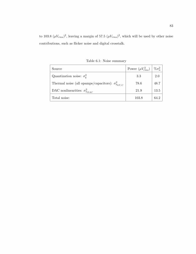
83
to 103.8 (µVrms)2, leaving a margin of 57.5 (µVrms)2, which will be used by other noise
contributions, such as flicker noise and digital crosstalk.
Table 6.1: Noise summary
Source Power (µV 2rms) %σ2
n
Quantization noise: σ2q 3.3 2.0
Thermal noise (all opamps/capacitors): σ2nkT/C
78.6 48.7
DAC nonlinearities: σ2nDAC
21.9 13.5
Total noise: 103.8 64.2
84
CHAPTER 7. PROTOTYPE CHIP DESIGN —
ANALOG SECTION
The analog section of the prototype chip, which contains the three ∆Σ modulator
stages, is described in this Chapter.
7.1. Modulator Stages
The circuit diagram of the first stage is illustrated in Figure 7.1. A single-ended
version is shown for clarity. All analog circuits were implemented in fully-differential
mode, and a detailed fully-differential schematic for the first stage is illustrated in Fig-
ure 7.2. In the fully-differential implementation, the capacitors values are half of those
shown in Fig. 7.1. This means that the noise power is increased by 6 dB6. However, since
the signal power is also increased by the same amount, the total performance in terms
of SNR is unchanged.
Figure 7.3 shows the schematic of the modulator used in the second and third
stages. Note that the reference voltage used in these stages is one quarter of the reference
voltage used in the first stage. This is necessary to implement the coefficient b = 1/4
shown previously in Figure 5.4.
6The noise power increases 3 dB due to the smaller capacitor values, and 3 dB due to having twiceas many noise sources.
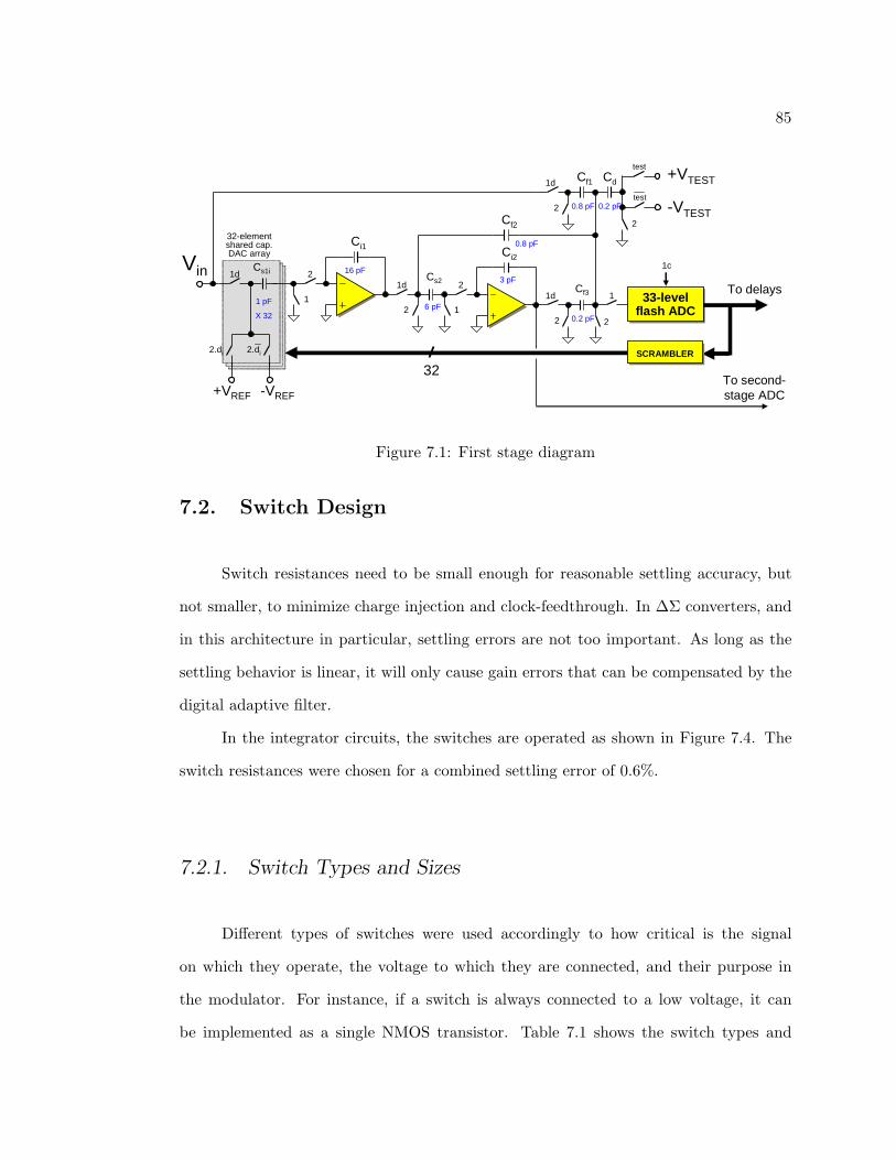
85
Vin 21d
1d
1
Ci1
Cs1iCs2
2 1
2
Ci2
1d
2
Cf3
2
1
Cf2
Cf1
2
1d
33-level flash ADC33-level
flash ADC
To second-stage ADC
2.di 2.di
+VREF -VREF
32-element shared cap. DAC array
32
2
Cd
test+VTEST
16 pF3 pF
0.8 pF
0.8 pF
6 pF
0.2 pF
0.2 pF
1 pF
X 32
SCRAMBLERSCRAMBLER
1c
-VTEST
test
To delays
Figure 7.1: First stage diagram
7.2. Switch Design
Switch resistances need to be small enough for reasonable settling accuracy, but
not smaller, to minimize charge injection and clock-feedthrough. In ∆Σ converters, and
in this architecture in particular, settling errors are not too important. As long as the
settling behavior is linear, it will only cause gain errors that can be compensated by the
digital adaptive filter.
In the integrator circuits, the switches are operated as shown in Figure 7.4. The
switch resistances were chosen for a combined settling error of 0.6%.
7.2.1. Switch Types and Sizes
Different types of switches were used accordingly to how critical is the signal
on which they operate, the voltage to which they are connected, and their purpose in
the modulator. For instance, if a switch is always connected to a low voltage, it can
be implemented as a single NMOS transistor. Table 7.1 shows the switch types and
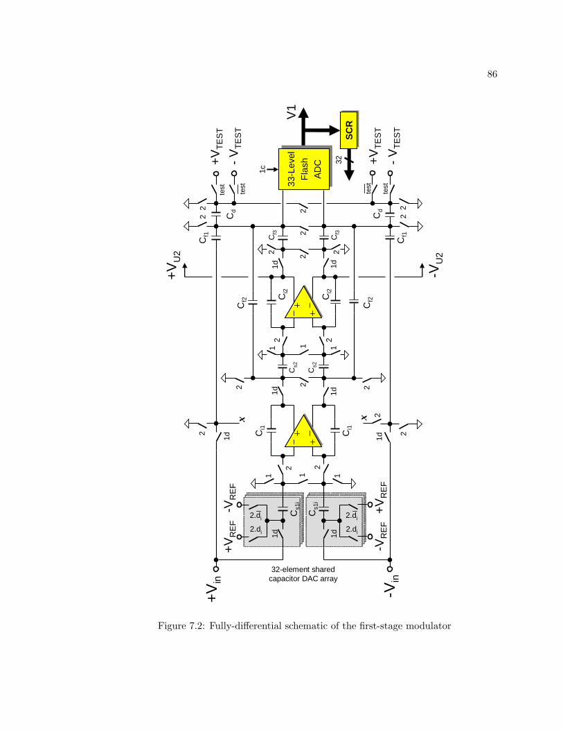
86
+V
in
2
1d1d
1C
i1
Cs1
iC
s2
2
21d
Cf3
2
Cf2
Cf1
2
Ci2
1d
1
32-element shared capacitor DAC array
Cd
SC
RS
CR
1c
V1
2.di
2.di
+V
RE
F-V
RE
F
Ci1
1d
Cs2
12
2
1d2
Cf3
33-L
evel
F
lash
A
DC
1d1
2C
s1i
Ci2
Cf2
-Vin
2
2
2.di
2.di
-VR
EF
+V
RE
F
2
test
+V
TE
ST
test
-V
TE
ST
2
test
-V
TE
ST
test
+V
TE
ST
11
22
2
Cd2
+V
U2
-VU
2
32
x
1d
2
2x
Cf1
Figure 7.2: Fully-differential schematic of the first-stage modulator
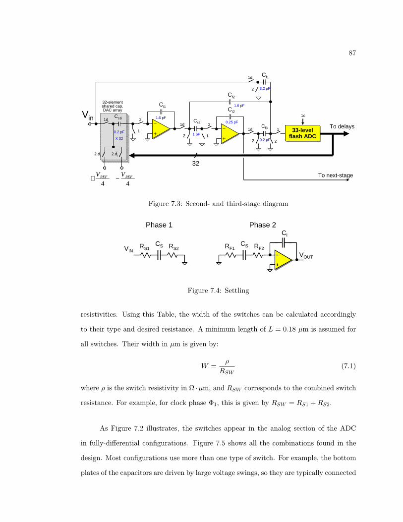
87
Vin 21d
1d
1
Ci1
Cs1iCs2
2 1
2
Ci2
1d
2
Cf3
2
1
Cf2
Cf1
2
1d
33-level flash ADC33-level
flash ADC
To next-stage
2.di 2.di
32-element shared cap. DAC array
32
1.6 pF0.25 pF
3.2 pF
1.6 pF
1 pF
0.2 pF
0.2 pF
X 32
1c
To delays
4REFV+
4REFV−
Figure 7.3: Second- and third-stage diagram
Phase 2
RF1 RF2CS
CI
Phase 1
RS1 RS2CSVIN
VOUT
Figure 7.4: Settling
resistivities. Using this Table, the width of the switches can be calculated accordingly
to their type and desired resistance. A minimum length of L = 0.18 µm is assumed for
all switches. Their width in µm is given by:
W =ρ
RSW(7.1)
where ρ is the switch resistivity in Ω ·µm, and RSW corresponds to the combined switch
resistance. For example, for clock phase Φ1, this is given by RSW = RS1 + RS2.
As Figure 7.2 illustrates, the switches appear in the analog section of the ADC
in fully-differential configurations. Figure 7.5 shows all the combinations found in the
design. Most configurations use more than one type of switch. For example, the bottom
plates of the capacitors are driven by large voltage swings, so they are typically connected
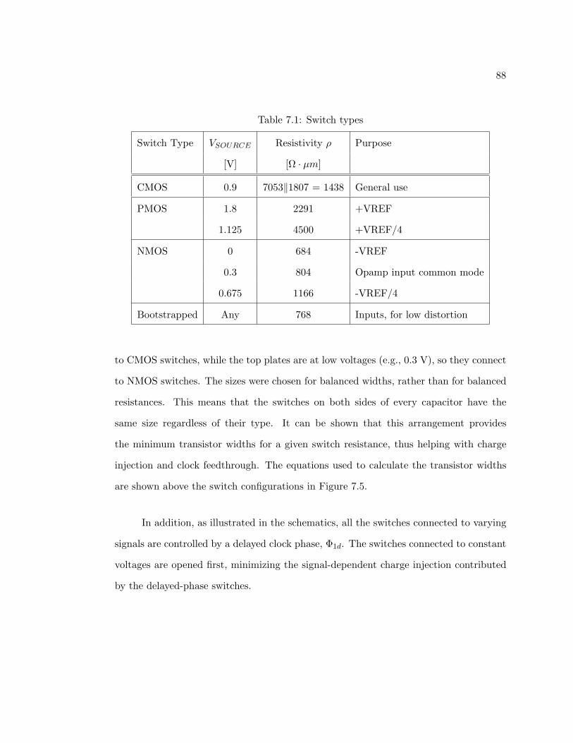
88
Table 7.1: Switch types
Switch Type VSOURCE Resistivity ρ Purpose
[V] [Ω · µm]
CMOS 0.9 7053‖1807 = 1438 General use
PMOS 1.8 2291 +VREF
1.125 4500 +VREF/4
NMOS 0 684 -VREF
0.3 804 Opamp input common mode
0.675 1166 -VREF/4
Bootstrapped Any 768 Inputs, for low distortion
to CMOS switches, while the top plates are at low voltages (e.g., 0.3 V), so they connect
to NMOS switches. The sizes were chosen for balanced widths, rather than for balanced
resistances. This means that the switches on both sides of every capacitor have the
same size regardless of their type. It can be shown that this arrangement provides
the minimum transistor widths for a given switch resistance, thus helping with charge
injection and clock feedthrough. The equations used to calculate the transistor widths
are shown above the switch configurations in Figure 7.5.
In addition, as illustrated in the schematics, all the switches connected to varying
signals are controlled by a delayed clock phase, Φ1d. The switches connected to constant
voltages are opened first, minimizing the signal-dependent charge injection contributed
by the delayed-phase switches.

89
W WC
W WC
WW C
WW C
WW C
WW C
WW C
WW C
2
W2
W2
W2
W
SWRW
2
2 21 ρρ +=SWR
W2
2 21 ρρ +=SWR
W 21 ρρ +=SWR
W2
21 ρρ +=
Figure 7.5: Switch configurations
7.2.2. Bootstrapped Switches
Some of the switches in the first stage operate directly on the input signal. For
large signal amplitudes, their nonlinear behavior — caused by signal-dependent resis-
tance, charge injection and clock feedthrough — becomes significant, introducing large
distortion components which limit the SNDR of the whole system. Figure 7.6 shows
where these switches are located. The switches in the DAC array are expected to be
critical, since distortion generated there is processed by a transfer function nearly similar
to the STF . The switch in the feedforward path is located in a seemingly low-sensitivity
node, since any harmonics generated there are attenuated by a second-order high-pass
transfer function. However, for this case, this is indeed a critical node: at OSR = 4,
high-frequency harmonics are poorly attenuated. For example, an harmonic at 12.5 MHz
is reduced by only 4.6 dB. Hence, both the DAC switches and feedforward switches are
operated with bootstrapped gate voltages.
There are a total of 66 such switches in the ADC. Half of them are connected
to VIN+, and the other half to VIN−. Therefore, only two bootstrapping circuits were
implemented to drive these two groups. A simplified diagram of the bootstrapping circuit
is shown in Figure 7.7.
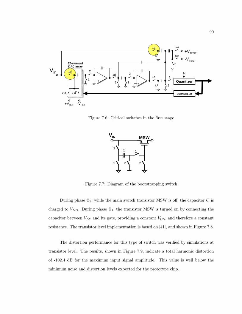
90
Vin 21d
12 1
2
2 2
1
2
1d
QuantizerQuantizer1d
2.di 2.di
+VREF -VREF
2
test
+VTEST
SCRAMBLERSCRAMBLER
1c
-VTEST
test
1d
32-element DAC array
Figure 7.6: Critical switches in the first stage
222
11C
VIN MSW
Figure 7.7: Diagram of the bootstrapping switch
During phase Φ2, while the main switch transistor MSW is off, the capacitor C is
charged to VDD. During phase Φ1, the transistor MSW is turned on by connecting the
capacitor between VIN and its gate, providing a constant VGS , and therefore a constant
resistance. The transistor level implementation is based on [41], and shown in Figure 7.8.
The distortion performance for this type of switch was verified by simulations at
transistor level. The results, shown in Figure 7.9, indicate a total harmonic distortion
of -102.4 dB for the maximum input signal amplitude. This value is well below the
minimum noise and distortion levels expected for the prototype chip.
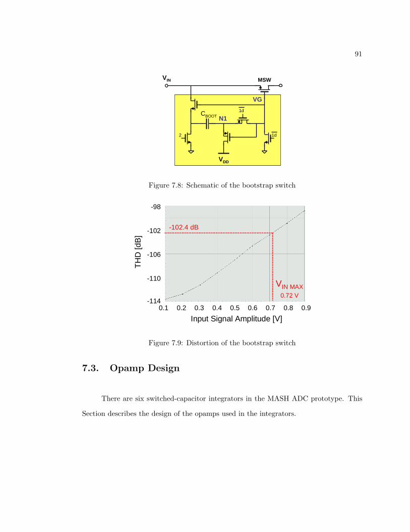
91
VDD
MSW
CBOOT
2
1d
VIN
N1
VG
1d
Figure 7.8: Schematic of the bootstrap switch
0.1 0.2 0.3 0.4 0.5 0.6 0.7 0.8 0.9-114
-110
-106
-102
-98
Input Signal Amplitude [V]
TH
D [d
B]
VIN MAX0.72 V
-102.4 dB
Figure 7.9: Distortion of the bootstrap switch
7.3. Opamp Design
There are six switched-capacitor integrators in the MASH ADC prototype. This
Section describes the design of the opamps used in the integrators.

92
7.3.1. Opamp Requirements
The opamps operate in the conditions shown in Figure 7.10. The capacitor Cp
shown in the Figure represents the input parasitic capacitance of the differential tran-
sistor pair. In general, opamp requirements were calculated for the integrating phase
(phase Φ2), since this is the configuration for which the slew rate and settling accuracy
are most important. However, settling accuracy is also important during the holding
phase (phase Φ1). When switching between the two configurations, the opamp has to
recover from glitches caused by clock feedthrough and charge injection, as well as other
disturbances. The opamp bandwidth was calculated to satisfy a 0.1% settling accuracy
during the integrating phase, and a 1.0% settling accuracy during the holding phase.
During Φ2 (integrating phase)During Φ1 (holding phase)CI
Cp
CNEXT
vo
CS
CI
Cpvo
Figure 7.10: Opamp configurations
The parameters for each opamp were determined, for Φ1 and Φ2, as follows:
1. Calculate the opamp load capacitance CL from coefficient and noise requirements
(done in Chapter 5 and 6).
2. Calculate the feedback factor β from the capacitor ratios.
3. Calculate the unity-gain frequency for 1% settling during Φ1, and 0.1% during Φ2:
ωUGBW1 = 4.6β1·tsett
, ωUGBW2 = 6.9β2·tsett
4. Calculate the slew-rate (only applicable during Φ2):
93
SR = ∆VMAXx·tsett
where x = 0.2 is the portion of the clock phase allowed for slewing effects; The
maximum voltage step, ∆VMAX , was obtained from system level simulations.
5. Calculate the effective transconductance value:
Gm = ωUGBW · CL
6. Find the bias current requirements from the slew rate SR:
ITAIL = SR · CL
7. Find the bias current requirements from Gm:
ITAIL = GmVEFF2
8. Choose the highest current.
As mentioned before, the opamp DC gain can be fairly low — the adaptive FIR
is supposed to take care of it — but a gain of 40∼50 dB was chosen due to noise and
linearity considerations.
This procedure was used to find the open-loop requirements for the six opamps.
The calculated values are shown in Table 7.2.
The values shown in the Table indicate that all the requirements can be covered
if only three different opamps are designed. The effective transconductances for these
three opamps are GmA > 54 mS, GmB > 11 mS, and GmC > 1.6 mS. The opamp with
the largest transconductance (GmA) is used for the first integrator in the first stage. The
opamp with the smallest transconductance (GmC) is used for the last integrator (the
second integrator in the third stage). The moderate transconductance GmB is used for
the remaining four opamps.
All opamps were implemented in folded-cascode topologies. The schematic is
shown in Figure 7.11. No additional gain boosting is required. The cascode transistors
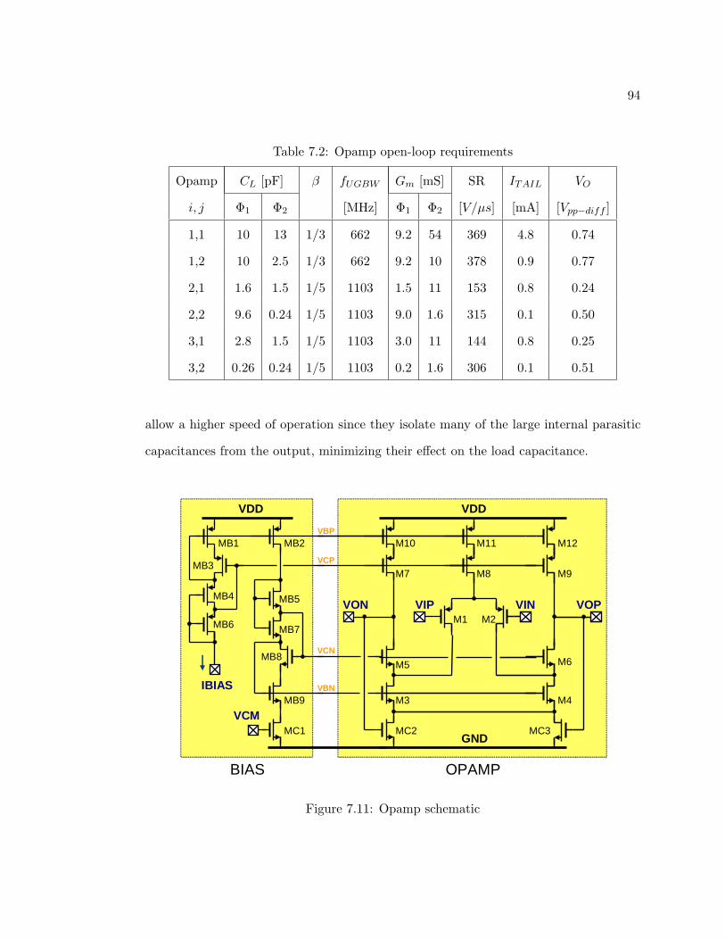
94
Table 7.2: Opamp open-loop requirements
Opamp CL [pF] β fUGBW Gm [mS] SR ITAIL VO
i, j Φ1 Φ2 [MHz] Φ1 Φ2 [V/µs] [mA] [Vpp−diff ]
1,1 10 13 1/3 662 9.2 54 369 4.8 0.74
1,2 10 2.5 1/3 662 9.2 10 378 0.9 0.77
2,1 1.6 1.5 1/5 1103 1.5 11 153 0.8 0.24
2,2 9.6 0.24 1/5 1103 9.0 1.6 315 0.1 0.50
3,1 2.8 1.5 1/5 1103 3.0 11 144 0.8 0.25
3,2 0.26 0.24 1/5 1103 0.2 1.6 306 0.1 0.51
allow a higher speed of operation since they isolate many of the large internal parasitic
capacitances from the output, minimizing their effect on the load capacitance.
VOPVON VINVIP
VDD
GND
OPAMP
VBN
VCN
VCP
VBP
M1 M2
M3 M4
M5 M6
M7 M9
M10 M12
MC2 MC3
M11
M8
BIAS
VCM
IBIAS
MB1 MB2
MB3
MB4 MB5
MB6 MB7
MB8
MB9
MC1
VDD
Figure 7.11: Opamp schematic
95
The selected common-mode feedback (CMFB) circuit operates in continuous time
[42]. It consists of the triode transistors MC1, MC2 and MC3. The transistor MC1
is used to adjust the common-mode voltage. The voltage drop VDS across MC2 and
MC3 decreases with the average of the opamp output voltages, achieving the desired
common-mode feedback operation.
The operation of this CMFB circuit is limited to output voltages above the thresh-
old voltage of the NMOS transistors, but having a wide output swing is not an important
requirement in this application, as indicated by the last column in Table 7.2.
7.3.2. Loop-Gain Specifications
Although the open-loop requirements are useful for the initial design of the opamps,
what ultimately matters during operation are the loop-gain parameters [43]. The opamps
must have enough loop-gain bandwidth and phase margin at all times, including during
the non-overlapping time between the clock phases. The loop-gain parameters were
found from transistor-level simulations, and are shown in Table 7.3 for all opamps.
As explained in Section 7.3.1., the settling error requirements are 1.0% for phase Φ1
and 0.1% for phase Φ2. These correspond to minimum loop bandwidths (fLGBW ) of
145 MHz and 220 MHz, respectively.
Two of the opamps shown in the Table have loop-gain bandwidths below the
required specifications. One is for opamp21 during phase Φ2 (fLGBW = 216 MHz).
This value is not significantly lower than the required, so it will be ignored; the other
is for opamp22 during phase Φ1 (fLGBW = 54 MHz). This value is excessively low, so
something must be done to improve it.

96
Table 7.3: Loop-gain specifications
Opamp Phase Φ1 Phase Φ2 Non-overlap
ij Gain fLGBW PM βeff Gain fLGBW PM βeff fLGBW PM
[dB] [MHz] [] [dB] [MHz] [] [MHz] []
11 A 45.6 1612 82 0.79 37.3 274 107 0.30 1722 65
12 B 46.1 165 95 0.71 38.3 269 108 0.29 1315 69
21 B 43.9 631 112 0.55 33.5 216 96 0.17 1337 69
22 B 33.7 54 93 0.17 29.1 577 101 0.10 837 77
31 B Same as opamp 21
32 C 43.5 727 97 0.58 33.0 265 113 0.17 1293 68
7.3.3. Opamp Problems
As Table 7.3 shows, the loop bandwidth of the second opamp in the second mod-
ulator (opamp22) is unacceptably low during phase Φ1. Unlike the other opamps, this
opamp has to drive very different load capacitances during the two clock phases. During
phase Φ2, the opamp is loaded only by its own feedback network (about 0.25 pF). During
phase Φ1, the opamp has to drive the input capacitance of the third ∆Σ modulator stage
(nearly 10 pF). Therefore, the settling behavior is too fast during phase Φ2, and too slow
during phase Φ1.
The reason for the slow behavior is the opamp’s input parasitic capacitance, Cp,
shown in Figure 7.12. This capacitance is too large when compared with the integrating
capacitor, degrading the feedback factor β during phase Φ1 (Eq. 7.2). If nothing is done,
the settling error during this phase can be as large as 20%.
β1 =CI
CI + Cp=
0.251.45
= 0.17 (7.2)
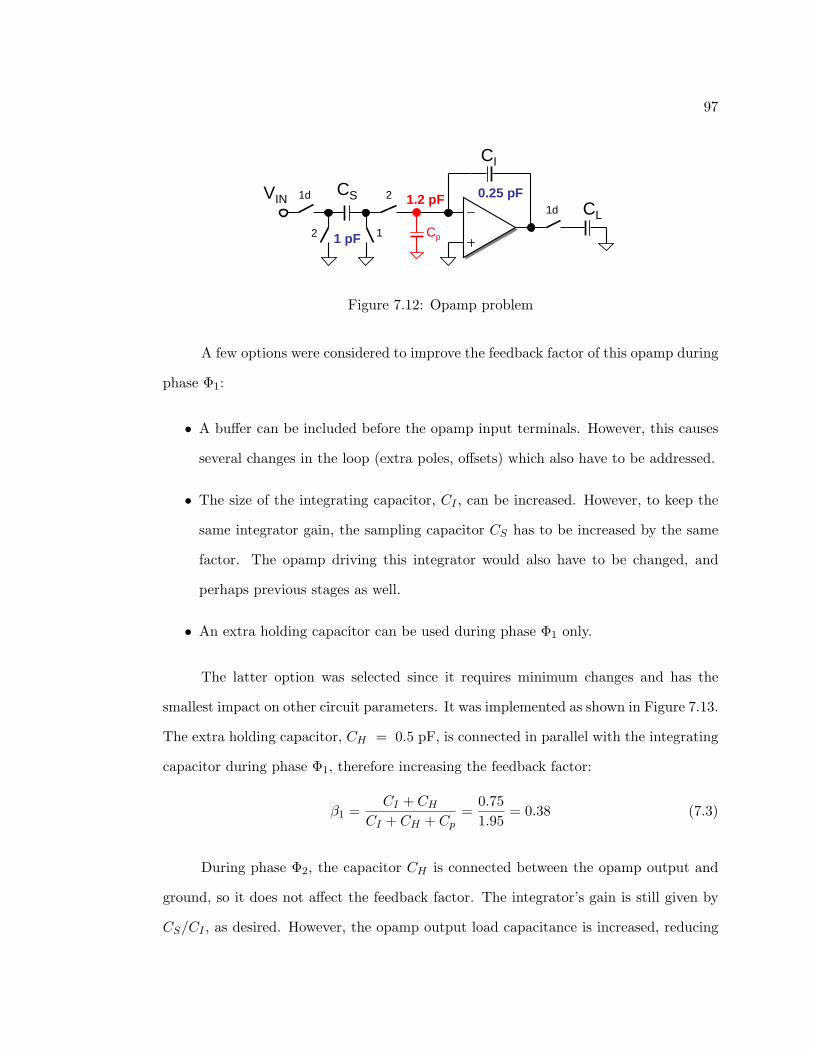
97
1d
2 1
2CS
CI
CL
1 pF
0.25 pFVIN
Cp
1.2 pF1d
Figure 7.12: Opamp problem
A few options were considered to improve the feedback factor of this opamp during
phase Φ1:
• A buffer can be included before the opamp input terminals. However, this causes
several changes in the loop (extra poles, offsets) which also have to be addressed.
• The size of the integrating capacitor, CI , can be increased. However, to keep the
same integrator gain, the sampling capacitor CS has to be increased by the same
factor. The opamp driving this integrator would also have to be changed, and
perhaps previous stages as well.
• An extra holding capacitor can be used during phase Φ1 only.
The latter option was selected since it requires minimum changes and has the
smallest impact on other circuit parameters. It was implemented as shown in Figure 7.13.
The extra holding capacitor, CH = 0.5 pF, is connected in parallel with the integrating
capacitor during phase Φ1, therefore increasing the feedback factor:
β1 =CI + CH
CI + CH + Cp=
0.751.95
= 0.38 (7.3)
During phase Φ2, the capacitor CH is connected between the opamp output and
ground, so it does not affect the feedback factor. The integrator’s gain is still given by
CS/CI , as desired. However, the opamp output load capacitance is increased, reducing
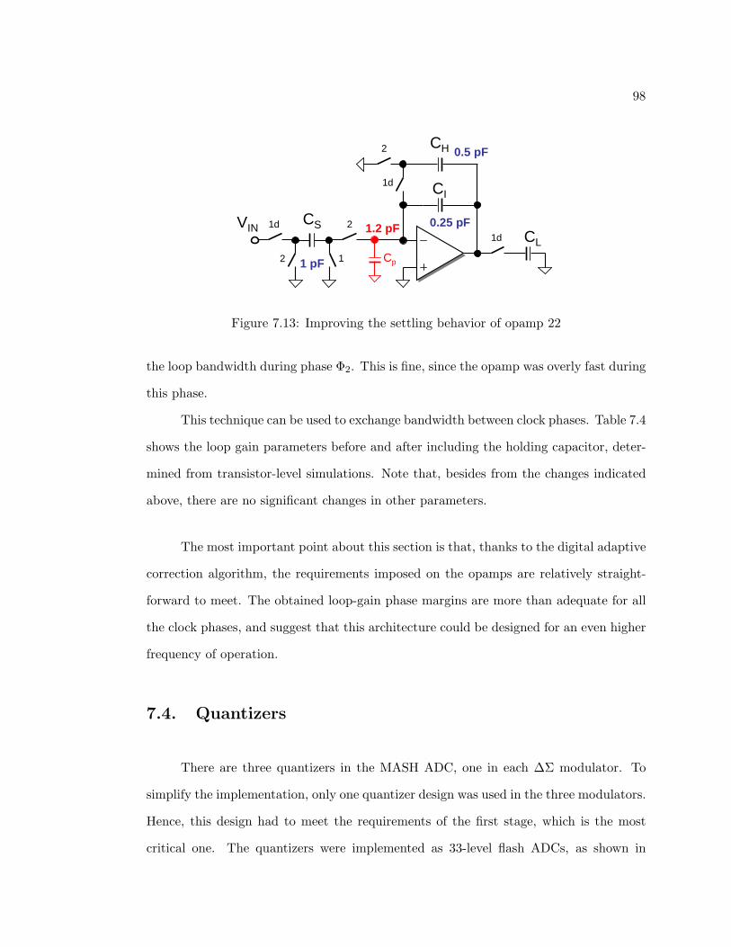
98
1d
2 1
2CS
CI
CL
1 pF
0.25 pF
CH2
1d
0.5 pF
VIN
Cp
1.2 pF1d
Figure 7.13: Improving the settling behavior of opamp 22
the loop bandwidth during phase Φ2. This is fine, since the opamp was overly fast during
this phase.
This technique can be used to exchange bandwidth between clock phases. Table 7.4
shows the loop gain parameters before and after including the holding capacitor, deter-
mined from transistor-level simulations. Note that, besides from the changes indicated
above, there are no significant changes in other parameters.
The most important point about this section is that, thanks to the digital adaptive
correction algorithm, the requirements imposed on the opamps are relatively straight-
forward to meet. The obtained loop-gain phase margins are more than adequate for all
the clock phases, and suggest that this architecture could be designed for an even higher
frequency of operation.
7.4. Quantizers
There are three quantizers in the MASH ADC, one in each ∆Σ modulator. To
simplify the implementation, only one quantizer design was used in the three modulators.
Hence, this design had to meet the requirements of the first stage, which is the most
critical one. The quantizers were implemented as 33-level flash ADCs, as shown in
99
Table 7.4: Loop-gain parameters with and without holding capacitor
Opamp 22 w/o CH w/ CH
Gain [dB] 33.7 40.6
Phase fLGBW [MHz] 54 105
Φ1 PM [] 93 93
βeff 0.17 0.38
Gain [dB] 29.1 29.1
Phase fLGBW [MHz] 577 243
Φ2 PM [] 101 106
βeff 0.10 0.10
Non-overlap fLGBW [MHz] 837 753
PM [] 77 78
Figure 7.14.
A resistor string generates the evenly-spaced threshold voltages used by the 32
comparators. A layer of bubble-correction logic, based on a voting scheme (2 out of
3) ensures that the resulting thermometer output code, in Q0 to Q31, has only one
transition7.
7.4.1. Effects of Passive Adder on Quantizer
A passive switched-capacitor adder is used in each modulator to combine the feed-
forward paths. The operation of this circuit is based on charge redistribution, causing a
reduction in signal swing, and therefore, in the input range of the quantizer following it.
7Bubble errors are incorrect comparator decisions, which can be caused by metastability, noise, andother nonideal effects.

100
.
.
.
VTP
VTN
Vin Y3131
1
0
Y1
Y0
RR
R
R
RR
bubblecorrection
bubblecorrection
bubblecorrection
‘1’
‘0’
.
.
.
Q31
Q1
Q0
Figure 7.14: Quantizer diagram
Referring to Figure 7.15, the input VIN of each quantizer is given by:
VIN =∑3
i=1 ViCFi
CIN +∑3
i=1 CFi
(7.4)
where CIN is the input capacitance of the quantizer, and the CFi are the feedforward
capacitors in the adder. This is a voltage division circuit which causes the attenuation
factor:
KF =VIN
V1=
CF1
CIN +∑3
i=1 CFi
(7.5)
This factor can be compensated by proper scaling (compression) of the quantizer thresh-
olds. It was done by adjusting the VTP and VTN voltages shown in Figure 7.14.
The input capacitance of the quantizer must be low, when compared with CF1, to
keep the attenuation factor KF within reasonable limits. If a quantizer input capacitance
of CIN = 1 pF is assumed, the accuracy requirements for the quantizer are as shown in

101
V1
V2
V3
CF1
CF2
CF3CIN
QuantizerVIN
Figure 7.15: Passive switched-capacitor adder during Φ1
Table 7.5: Quantizer requirements
First Stage Second and Third Stages
Passive Adder Gain KF 0.29 0.53
VLSB for 5-bit resolution [mV] 16.3 29.8
∆VLSB for 7-bit linearity [mV] 4.1 7.4
Table 7.5. The resolution and accuracy values shown in the Table were calculated from:
VLSB = VREF KF /32 ∆VLSB = VREF KF /128 (7.6)
where VREF = 1.8 V.
7.4.2. Comparator Design
From the results derived in the previous Section, each comparator must have an
accuracy of 4.1 mV to meet the 7-bit linearity requirements of the first stage. In addition,
a quantizer input capacitance of CIN ≤ 1 pF means that each comparator must have
an input capacitance CIN/32 ≤ 31.25 fF. Finally, since there a total of 96 comparators
in the prototype, a low power consumption is desirable.
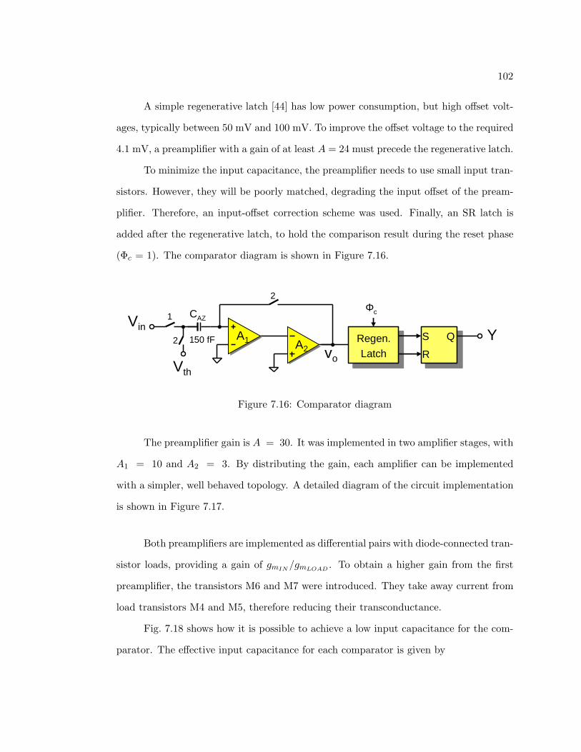
102
A simple regenerative latch [44] has low power consumption, but high offset volt-
ages, typically between 50 mV and 100 mV. To improve the offset voltage to the required
4.1 mV, a preamplifier with a gain of at least A = 24 must precede the regenerative latch.
To minimize the input capacitance, the preamplifier needs to use small input tran-
sistors. However, they will be poorly matched, degrading the input offset of the pream-
plifier. Therefore, an input-offset correction scheme was used. Finally, an SR latch is
added after the regenerative latch, to hold the comparison result during the reset phase
(Φc = 1). The comparator diagram is shown in Figure 7.16.
Vin1
2 Regen. Latch
S QA1 A2Y
Φc
RVth
150 fF
2
vo
CAZ
Figure 7.16: Comparator diagram
The preamplifier gain is A = 30. It was implemented in two amplifier stages, with
A1 = 10 and A2 = 3. By distributing the gain, each amplifier can be implemented
with a simpler, well behaved topology. A detailed diagram of the circuit implementation
is shown in Figure 7.17.
Both preamplifiers are implemented as differential pairs with diode-connected tran-
sistor loads, providing a gain of gmIN /gmLOAD . To obtain a higher gain from the first
preamplifier, the transistors M6 and M7 were introduced. They take away current from
load transistors M4 and M5, therefore reducing their transconductance.
Fig. 7.18 shows how it is possible to achieve a low input capacitance for the com-
parator. The effective input capacitance for each comparator is given by
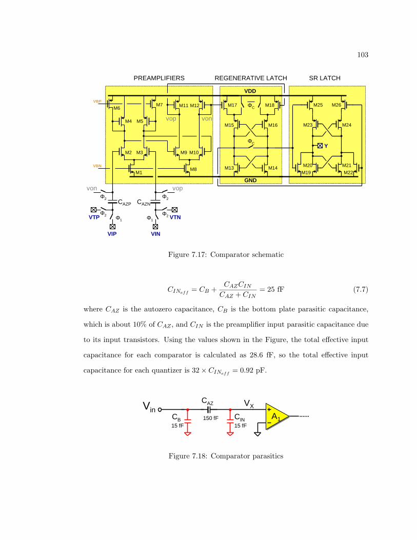
103
VDD
GND
M17 M18
M15 M16
M13 M14
ΦC
ΦC
REGENERATIVE LATCH
VINVIP
VBP
M6M7
M2 M3
VBN
M4 M5
M1
M9 M10
M11 M12
M8
VTP VTNΦ1Φ1Φ2Φ2
Φ2Φ2
vop von
vopvon
PREAMPLIFIERS
M25 M26
M23 M24
M20 M21
SR LATCH
M19 M22
Y
CAZP CAZN
Figure 7.17: Comparator schematic
CINeff= CB +
CAZCIN
CAZ + CIN= 25 fF (7.7)
where CAZ is the autozero capacitance, CB is the bottom plate parasitic capacitance,
which is about 10% of CAZ , and CIN is the preamplifier input parasitic capacitance due
to its input transistors. Using the values shown in the Figure, the total effective input
capacitance for each comparator is calculated as 28.6 fF, so the total effective input
capacitance for each quantizer is 32× CINeff= 0.92 pF.
VinA1
CAZ
150 fF15 fF15 fF
CINCB
VX
Figure 7.18: Comparator parasitics

104
The regenerative latch is based on [45]. Transistors M13, M14, M15 and M16 form
the positive-feedback amplifier, which is active even during the reset phase Φc. Although
this type of latch consumes power during both phases, it has a higher accuracy and a
higher speed of operation than if it was turned off during the reset phase.
The power consumption for each comparator is 450 µW, for a 1.8 V supply. The
32 comparators in each quantizer consume a total of 14.4 mW.
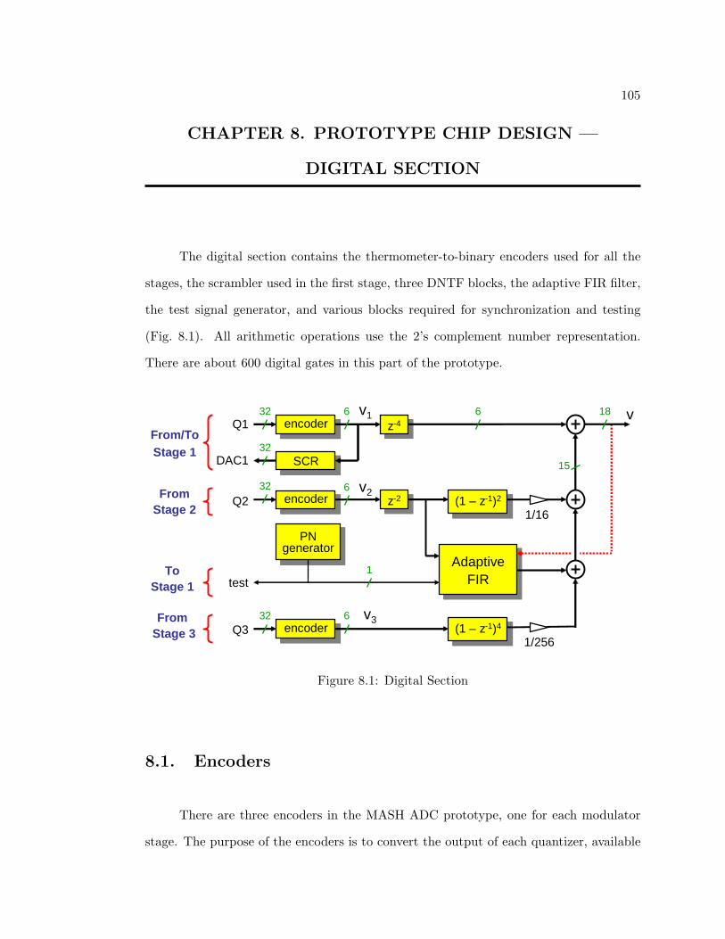
105
CHAPTER 8. PROTOTYPE CHIP DESIGN —
DIGITAL SECTION
The digital section contains the thermometer-to-binary encoders used for all the
stages, the scrambler used in the first stage, three DNTF blocks, the adaptive FIR filter,
the test signal generator, and various blocks required for synchronization and testing
(Fig. 8.1). All arithmetic operations use the 2’s complement number representation.
There are about 600 digital gates in this part of the prototype.
v1z-4
vencoder
1/16
v2z-2
v3(1 – z-1)4
(1 – z-1)2
1/256
Adaptive FIR
encoder
encoder
SCR
32
32
32
32
6
6
6
18
15
PN generator
test
From/ToStage 1
FromStage 2
FromStage 3
ToStage 1
Q1
DAC1
Q2
Q3
6
1
Figure 8.1: Digital Section
8.1. Encoders
There are three encoders in the MASH ADC prototype, one for each modulator
stage. The purpose of the encoders is to convert the output of each quantizer, available
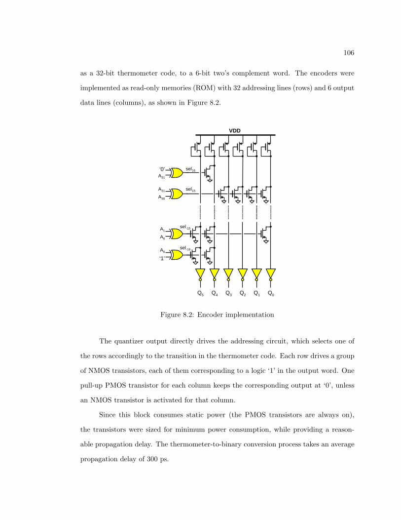
106
as a 32-bit thermometer code, to a 6-bit two’s complement word. The encoders were
implemented as read-only memories (ROM) with 32 addressing lines (rows) and 6 output
data lines (columns), as shown in Figure 8.2.
‘0’A31
A31
A30
VDD
A1
A0
A0
‘1’
Q5 Q4 Q3 Q2 Q1 Q0
sel16
sel15
sel-15
sel-16
Figure 8.2: Encoder implementation
The quantizer output directly drives the addressing circuit, which selects one of
the rows accordingly to the transition in the thermometer code. Each row drives a group
of NMOS transistors, each of them corresponding to a logic ‘1’ in the output word. One
pull-up PMOS transistor for each column keeps the corresponding output at ‘0’, unless
an NMOS transistor is activated for that column.
Since this block consumes static power (the PMOS transistors are always on),
the transistors were sized for minimum power consumption, while providing a reason-
able propagation delay. The thermometer-to-binary conversion process takes an average
propagation delay of 300 ps.
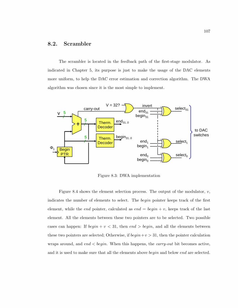
107
8.2. Scrambler
The scrambler is located in the feedback path of the first-stage modulator. As
indicated in Chapter 5, its purpose is just to make the usage of the DAC elements
more uniform, to help the DAC error estimation and correction algorithm. The DWA
algorithm was chosen since it is the most simple to implement.
5v
Begin PTR
Φ1
Therm. Decoder
begin31..0
end31..0
to DAC switches
5
5 Therm. Decoder
carry-out
end0 select0begin0
select1begin1
end1
end31begin31
select31
V = 32? invert
Figure 8.3: DWA implementation
Figure 8.4 shows the element selection process. The output of the modulator, v,
indicates the number of elements to select. The begin pointer keeps track of the first
element, while the end pointer, calculated as end = begin + v, keeps track of the last
element. All the elements between these two pointers are to be selected. Two possible
cases can happen: If begin + v < 31, then end > begin, and all the elements between
these two pointers are selected; Otherwise, if begin+v > 31, then the pointer calculation
wraps around, and end < begin. When this happens, the carry-out bit becomes active,
and it is used to make sure that all the elements above begin and below end are selected.
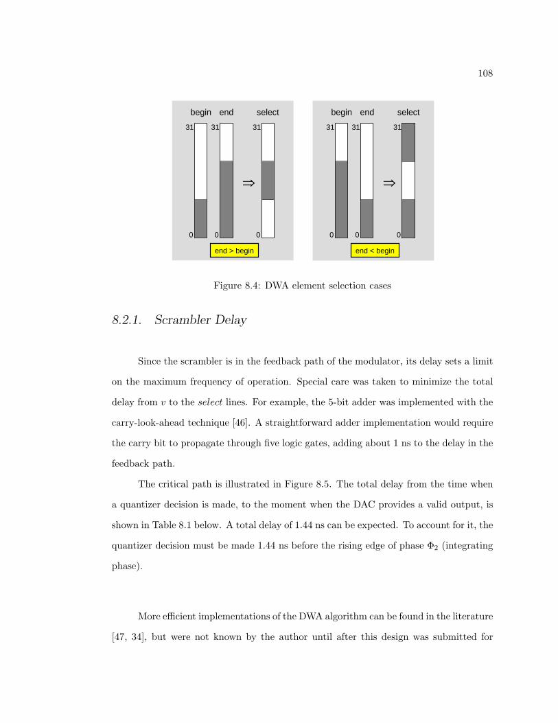
108
begin end select
0
31
⇒
0
31
0
31
begin end select
0
31
⇒
0
31
0
31
end > begin end < begin
Figure 8.4: DWA element selection cases
8.2.1. Scrambler Delay
Since the scrambler is in the feedback path of the modulator, its delay sets a limit
on the maximum frequency of operation. Special care was taken to minimize the total
delay from v to the select lines. For example, the 5-bit adder was implemented with the
carry-look-ahead technique [46]. A straightforward adder implementation would require
the carry bit to propagate through five logic gates, adding about 1 ns to the delay in the
feedback path.
The critical path is illustrated in Figure 8.5. The total delay from the time when
a quantizer decision is made, to the moment when the DAC provides a valid output, is
shown in Table 8.1 below. A total delay of 1.44 ns can be expected. To account for it, the
quantizer decision must be made 1.44 ns before the rising edge of phase Φ2 (integrating
phase).
More efficient implementations of the DWA algorithm can be found in the literature
[47, 34], but were not known by the author until after this design was submitted for
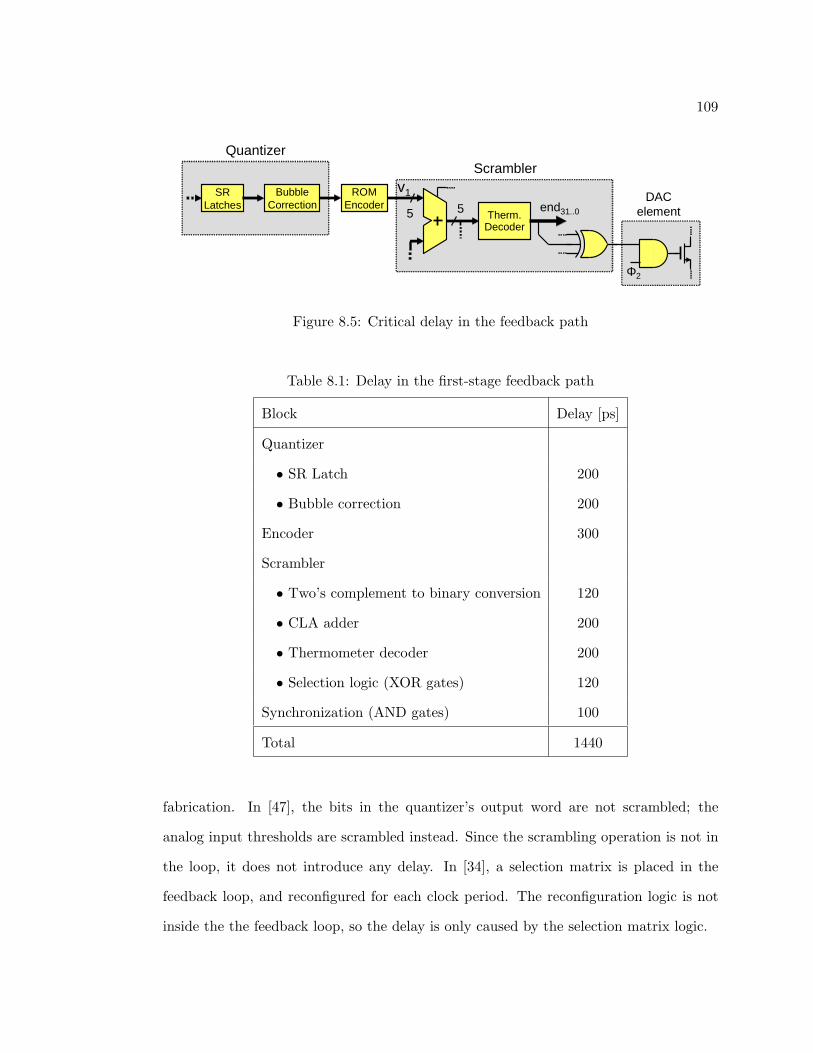
109
5
v1
Therm. Decoder
end31..0
DAC element5
BubbleCorrection
ROMEncoder
Φ2
Scrambler
SRLatches
Quantizer
Figure 8.5: Critical delay in the feedback path
Table 8.1: Delay in the first-stage feedback path
Block Delay [ps]
Quantizer
• SR Latch 200
• Bubble correction 200
Encoder 300
Scrambler
• Two’s complement to binary conversion 120
• CLA adder 200
• Thermometer decoder 200
• Selection logic (XOR gates) 120
Synchronization (AND gates) 100
Total 1440
fabrication. In [47], the bits in the quantizer’s output word are not scrambled; the
analog input thresholds are scrambled instead. Since the scrambling operation is not in
the loop, it does not introduce any delay. In [34], a selection matrix is placed in the
feedback loop, and reconfigured for each clock period. The reconfiguration logic is not
inside the the feedback loop, so the delay is only caused by the selection matrix logic.
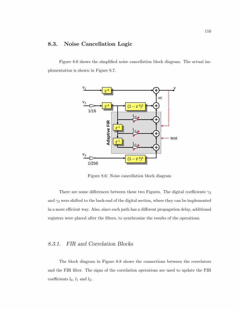
110
8.3. Noise Cancellation Logic
Figure 8.6 shows the simplified noise cancellation block diagram. The actual im-
plementation is shown in Figure 8.7.
v1z-4
v2z-2
v3(1 – z-1)4
(1 – z-1)2
z-1
z-1
1/16
1/256
L0
L1
L2
v
vc
Ad
apti
ve F
IR
test
Figure 8.6: Noise cancellation block diagram
There are some differences between these two Figures. The digital coefficients γ2
and γ3 were shifted to the back-end of the digital section, where they can be implemented
in a more efficient way. Also, since each path has a different propagation delay, additional
registers were placed after the filters, to synchronize the results of the operations.
8.3.1. FIR and Correlation Blocks
The block diagram in Figure 8.8 shows the connections between the correlators
and the FIR filter. The signs of the correlation operations are used to update the FIR
coefficients l0, l1 and l2.
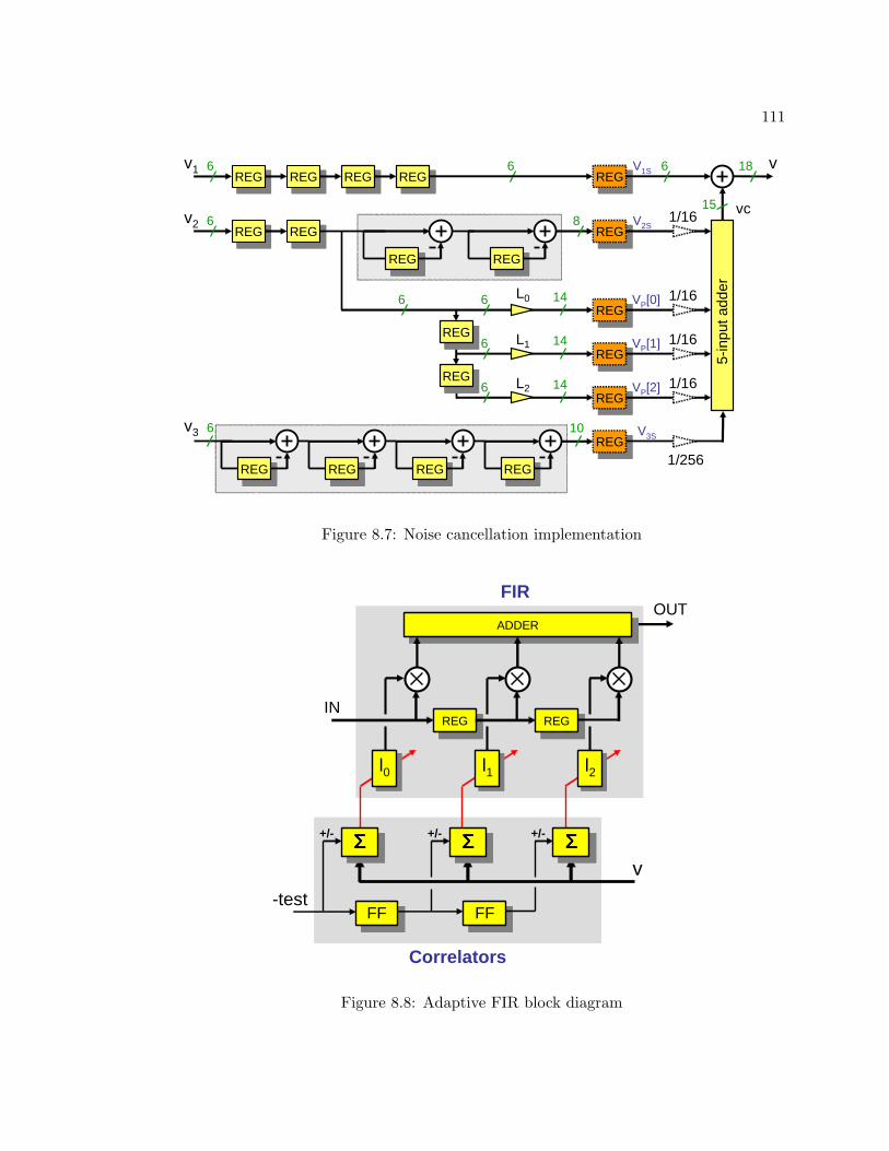
111
REG
REG
REG
REG
REG
REG
v1
REGv2
v3
1/16
1/256
L0
L1
L2
v
vc
REG REG REG
REG
REG
REG
REG REG
5-in
put a
dder
REG REG REG
1/16
1/16
1/16
6
6
6
6 6
14
14
14
10
158
18
6 6
6
6
V2S
VP[0]
VP[1]
VP[2]
V1S
V3S
REG
REG
Figure 8.7: Noise cancellation implementation
REGREG REGREG
FIR
IN
OUT
FFFF FFFF-test
v
Correlators
+/- +/- +/-ΣΣΣΣΣΣΣΣ ΣΣΣΣΣΣΣΣ ΣΣΣΣΣΣΣΣ
ADDERADDER
l0 l1 l2
Figure 8.8: Adaptive FIR block diagram
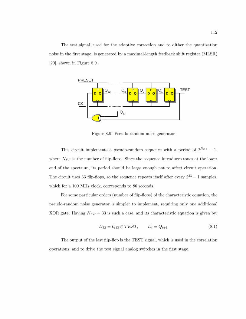
112
The test signal, used for the adaptive correction and to dither the quantization
noise in the first stage, is generated by a maximal-length feedback shift register (MLSR)
[20], shown in Figure 8.9.
D QP
D QP
D QPQ32 Q1
CK
TESTD Q
P
PRESET
Q2
Q13
Q3
Figure 8.9: Pseudo-random noise generator
This circuit implements a pseudo-random sequence with a period of 2NFF − 1,
where NFF is the number of flip-flops. Since the sequence introduces tones at the lower
end of the spectrum, its period should be large enough not to affect circuit operation.
The circuit uses 33 flip-flops, so the sequence repeats itself after every 233 − 1 samples,
which for a 100 MHz clock, corresponds to 86 seconds.
For some particular orders (number of flip-flops) of the characteristic equation, the
pseudo-random noise generator is simpler to implement, requiring only one additional
XOR gate. Having NFF = 33 is such a case, and its characteristic equation is given by:
D32 = Q13 ⊕ TEST, Di = Qi+1 (8.1)
The output of the last flip-flop is the TEST signal, which is used in the correlation
operations, and to drive the test signal analog switches in the first stage.

113
8.3.2. FIR Coefficients
The FIR coefficients are updated by the correlators in the adaptive filter. In their
simplest form, they can be implemented as up/down counters. However, for testing
purposes, it is desirable to have different adaptation steps. A large adaptation step
means that the adaptive algorithm is fast to converge, but noisy after convergence, while
a small adaptation step means a longer convergence time, but less noise due to coefficient
variations.
Therefore, the FIR coefficients were implemented as accumulators, as shown in
Fig. 8.10. The adaptation steps can be selected from four different values. One of them
is zero, in which case the adaptation process is “frozen”. In this mode, the correlators
still perform their function as usual, but the coefficients are not updated. Each step
is added or subtracted to the FIR coefficient accordingly to the sign of the result for
the corresponding correlator calculation, as described in Section 4.2.3. for the SSBLMS
algorithm.
14
14
CI
REG
ADD/SUB
Q13..0
000h
001h
002h
004h
MUX14
2
Adaptation StepSelection
SCK
Figure 8.10: FIR coefficient
The width of the coefficients was selected at 14 bits, based on system level simu-
lations, with their effect on the corrected SNDR being taken into account. The output
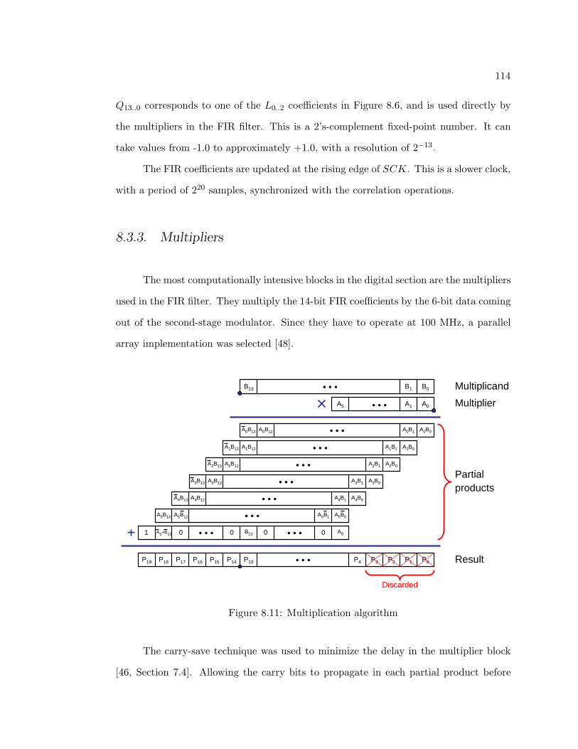
114
Q13..0 corresponds to one of the L0..2 coefficients in Figure 8.6, and is used directly by
the multipliers in the FIR filter. This is a 2’s-complement fixed-point number. It can
take values from -1.0 to approximately +1.0, with a resolution of 2−13.
The FIR coefficients are updated at the rising edge of SCK. This is a slower clock,
with a period of 220 samples, synchronized with the correlation operations.
8.3.3. Multipliers
The most computationally intensive blocks in the digital section are the multipliers
used in the FIR filter. They multiply the 14-bit FIR coefficients by the 6-bit data coming
out of the second-stage modulator. Since they have to operate at 100 MHz, a parallel
array implementation was selected [48].
B13
A0A1A5
A0B0
• • •
A0B1A0B13
A1B0A1B1A1B13
A2B0A2B1A2B13
A0B12
A1B12
• • •
A2B12
A3B0A3B1A3B13 A3B12
A4B0A4B1A4B13 A4B12
A5B0A5B1A5B13 A5B12
A5+B13 B13 A50 0• • •0• • •1
P0P1P2P3P19 P18 P17 P16 • • •
0
B0B1• • •
• • •
• • •
• • •
• • •
• • •
Multiplicand
Multiplier
Result
Partial products
P15 P4
Discarded
P14 P13
Figure 8.11: Multiplication algorithm
The carry-save technique was used to minimize the delay in the multiplier block
[46, Section 7.4]. Allowing the carry bits to propagate in each partial product before

115
starting the next addition would be very inefficient. Instead, each carry bit is propagated
down diagonally through the multiplier structure.
8.3.4. Correlators
The correlators were implemented as accumulators, as shown in Figure 8.12. Their
purpose is simply to add or subtract samples of the output v, accordingly to the sign of
the test signal. Since the output v is an 18-bit signal, and 220 samples are accumulated
before restarting the correlation, the accumulators require 18+20=38 bits, in the worst
case, to store the result of the correlation operation.
18
38
CI REG
ADD/SUB
Q37..0
V 18
CK
RESTART
MSB (sign)
Figure 8.12: Correlator
The MSB of each accumulated result is the sign bit. It is used to update the corre-
sponding FIR coefficient. It connects to the ADD/SUB input line shown in Figure 8.10.
8.3.5. Synchronization
The synchronization block (Figure 8.13) creates control signals needed for the
adaptive FIR block. The correlators operate on blocks of 220 samples. Every time
a calculation is complete, the result is used to update the FIR coefficients, and the
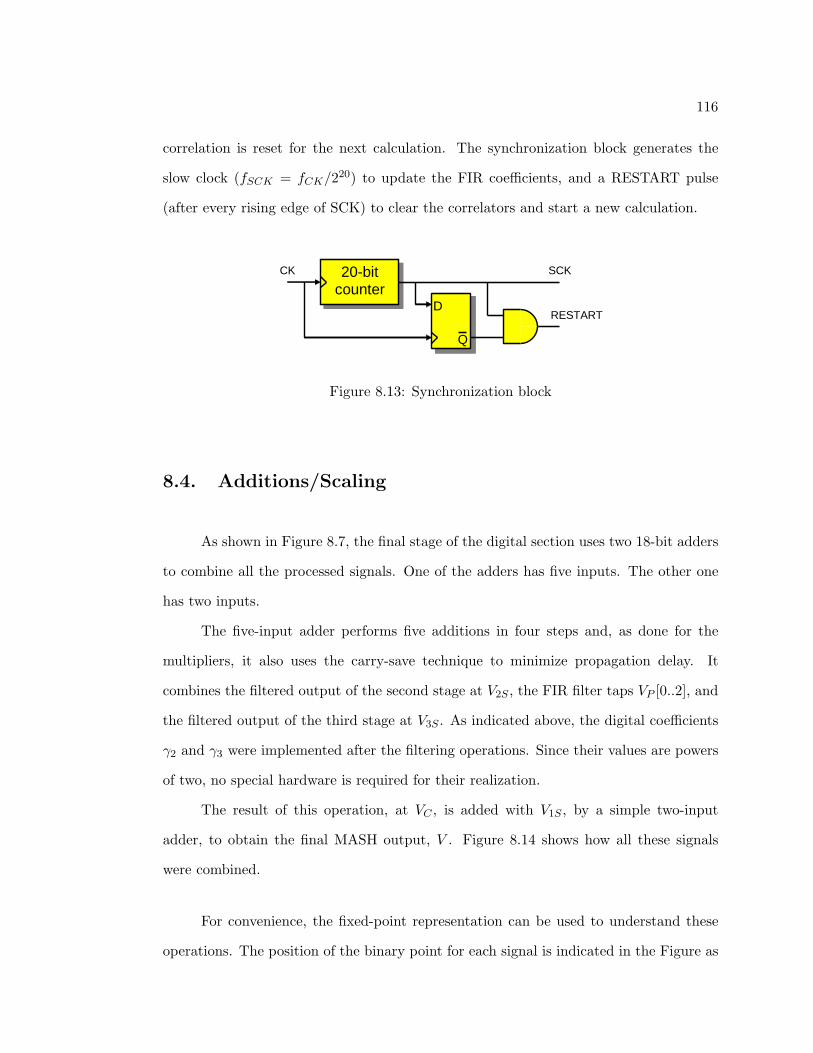
116
correlation is reset for the next calculation. The synchronization block generates the
slow clock (fSCK = fCK/220) to update the FIR coefficients, and a RESTART pulse
(after every rising edge of SCK) to clear the correlators and start a new calculation.
20-bit counter
CK SCK
RESTARTD
Q
Figure 8.13: Synchronization block
8.4. Additions/Scaling
As shown in Figure 8.7, the final stage of the digital section uses two 18-bit adders
to combine all the processed signals. One of the adders has five inputs. The other one
has two inputs.
The five-input adder performs five additions in four steps and, as done for the
multipliers, it also uses the carry-save technique to minimize propagation delay. It
combines the filtered output of the second stage at V2S , the FIR filter taps VP [0..2], and
the filtered output of the third stage at V3S . As indicated above, the digital coefficients
γ2 and γ3 were implemented after the filtering operations. Since their values are powers
of two, no special hardware is required for their realization.
The result of this operation, at VC , is added with V1S , by a simple two-input
adder, to obtain the final MASH output, V . Figure 8.14 shows how all these signals
were combined.
For convenience, the fixed-point representation can be used to understand these
operations. The position of the binary point for each signal is indicated in the Figure as

117
13 910 01812 11 . . .
13 910 01812 11 . . .
13 910 01812 11 . . .
VP[0]/16
VP[1]/16
VP[2]/16
V2S/16 3 02 1. . . 7
V3S/256
1314 1216 15 . . . 23VC
02 1. . . 9 8 3
3 02 15 4V1S
1112 1014 13 . . . 01V 151617
Sign Ex.
Sign Ex.
Sign Ex.
S.E.
Padded with zeros
Padded w/ zeros
Padded with zeros
Five-Input Adder
(18-bit)
Two-Input Adder(18-bit)
S.E.
Discarded
1 0
Figure 8.14: Scaling and additions
a small dot, separating the integer part from the fractional part. Note that the binary
points of V2S and VP [0..2] were shifted 4 bits to the right of the final output. This is
how γ2 = 1/16 was implemented. Also, the binary point of V3S is 8 bits to the right,
implementing γ3 = 1/256.
8.5. Clock generator
The clock generator creates the non-overlapping clock phases used in the analog
section of the chip (Figure 8.15).
As explained in Section 7.2., a delayed version of clock phase Φ1 is used to help
reducing the effects of signal dependent charge injection and clock feedthrough. This
delayed clock phase Φ1d has a delayed falling time, but it should not have a delayed
rising time, since that would reduce the total available settling time. Transistor M1
makes sure that the phases Φ1 and Φ1d rise at the same time.
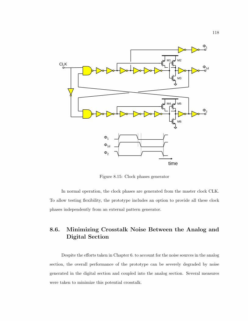
118
Φ1
Φ1d
Φ2
CLKM1 M2
M3
M4 M5
M6
Φ1
Φ1d
Φ2
time
Figure 8.15: Clock phases generator
In normal operation, the clock phases are generated from the master clock CLK.
To allow testing flexibility, the prototype includes an option to provide all these clock
phases independently from an external pattern generator.
8.6. Minimizing Crosstalk Noise Between the Analog andDigital Section
Despite the efforts taken in Chapter 6. to account for the noise sources in the analog
section, the overall performance of the prototype can be severely degraded by noise
generated in the digital section and coupled into the analog section. Several measures
were taken to minimize this potential crosstalk.

119
• The opamps, quantizers, switch drivers and the digital section use independent
supply rails and substrate connections. The NMOS transistors in the digital section
have independent ground and substrate tap connections, preventing the digital
switching noise in the ground rail from coupling into the substrate.
• The digital logic operates on the falling edge of phase Φ2. This way, most digital
noise will occur during the non-overlapping time, and during the initial part of the
sampling phase Φ1. By the time the analog signals are sampled, most of the digital
logic should be quiet.
• The opamp bias currents in the first stage are independent. Since the second
and third stages are less critical, the two opamps in each of the stages share the
bias network. Also, the bias current used in each of the three quantizers can be
independently adjusted.
• The capacitors used in the integrators and passive adders sit on top of an N-well
with a dedicated ground connection. This acts as a shield which prevents substrate
noise from coupling into the capacitors.
• During layout, special attention was given to the routing of critical signals. Where
possible, short traces were used. For the most part, signal crossings were avoided.
In the cases where they could not be avoided, shielding and fully-differential routing
was employed.
• Logic gates used in non-critical operations were selected for slower transitions,
reducing the amount of noise coupling to other circuits.
8.7. Output Interface and Test Modes
Several signals need to be acquired in order to fully assess the performance of the
MASH ADC prototype. These signals include the primary MASH output, denoted as V ,
120
which is an 18-bit wide bus, and the DAC element selection vector, which is a 32-bit wide
bus. Just for these two signals, the prototype package would require 50 pins, which is
a prohibitively large number of pins. Therefore, the following considerations were made
to reduce it without sacrificing functionality or accessibility:
• The 32-bit DAC element selection vector can be fully replicated off-line by acquiring
the output of the first stage, at V1, and the begin pointer in the DWA algorithm.
Together, these two signals require only 11 pins.
• Consider the diagram of the digital section, shown in Figure 8.1. The 18-bit output
V is built from the output V1 of the first stage, and the 15-bit signal VC . Since V1
is made available for the DAC element selection vector, the signal VC can be made
available as a chip output, instead of V , therefore saving 3 pins. The MASH output
V can be reproduced off-line from these two signals. The signal V is still calculated
inside the prototype, since it is required by the digital adaptive correction scheme.
However, it is not necessary to make it accessible off-chip.
With these considerations, the MASH output interface can be implemented with only
26 pins, instead of 50 pins.
The prototype includes digital and analog test modes. They can provide more
details about the operation of each stage and, in case something does not operate as
expected, it provides access to the analog and digital signals in the system for trou-
bleshooting purposes.
To implement the digital test modes, a multiplexer was used to switch between the
normal operating mode and the desired digital signals. These latter include the outputs
of all ∆Σ modulators, the test signal, and the three adaptive filter coefficients.
To implement the analog test modes, the chip includes static analog switches
controlled by another multiplexer. The outputs of any of the integrators can be observed,
and it is possible to apply an input signal directly to the second or third modulator stages
to verify their functionality independently.

121
8.8. Layout Considerations
Figure 8.16 shows the layout of the MASH ADC. As the Figure shows, the digital
adaptive filter occupies only about 10% of the total active area. The FIR block includes
the multipliers, the filter coefficients, the correlators and the synchronization logic for
the three filter taps.
The active area measures 1 by 2 mm2. The design was implemented in a 0.18 µm
CMOS process provided by National Semiconductor.
CLKQuantizers
FIRDW
A
ADC1 ADC2 ADC3
Opamps
Capacitors
Digital Section
Switches
Switches
Q25..Q0
VIN, VREF, VCM, etc
Q1 Q2 Q3
Figure 8.16: Layout
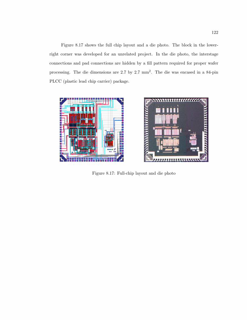
122
Figure 8.17 shows the full chip layout and a die photo. The block in the lower-
right corner was developed for an unrelated project. In the die photo, the interstage
connections and pad connections are hidden by a fill pattern required for proper wafer
processing. The die dimensions are 2.7 by 2.7 mm2. The die was encased in a 84-pin
PLCC (plastic lead chip carrier) package.
Figure 8.17: Full-chip layout and die photo
123
CHAPTER 9. TEST SETUP AND EXPERIMENTAL
RESULTS
This Chapter describes the test setup and experimental results obtained from the
prototype chip.
9.1. Test Board Design
To achieve the expected performance of the prototype chip, a good test board
design is of utmost importance. The test board uses six layers, as shown in Figure 9.1.
The purpose of each of the layers in the board is also shown. Several steps were taken
to ensure good testing conditions:
• Ground plane:
Analog and digital sections use a common ground plane. The ground plane was
implemented in three of the six layers, interconnected with vias. Multiple ground
vias were placed directly under the chip, making this a low resistance area, and
ensuring that the analog and digital signals are referred to a common potential.
• Decoupling of power, reference and bias pins:
Ceramic capacitors of 0.1 µF and 0.01 µF were placed near the chip pins, for high-
frequency decoupling. Tantalum capacitors from 2.2 µF to 10 µF were placed near
the voltage sources, for low-frequency decoupling [49].
• Signals generating large amounts of noise (clock, digital outputs) were implemented
with short traces, and their transitions were slowed down to reduce electromagnetic
interference (EMI).
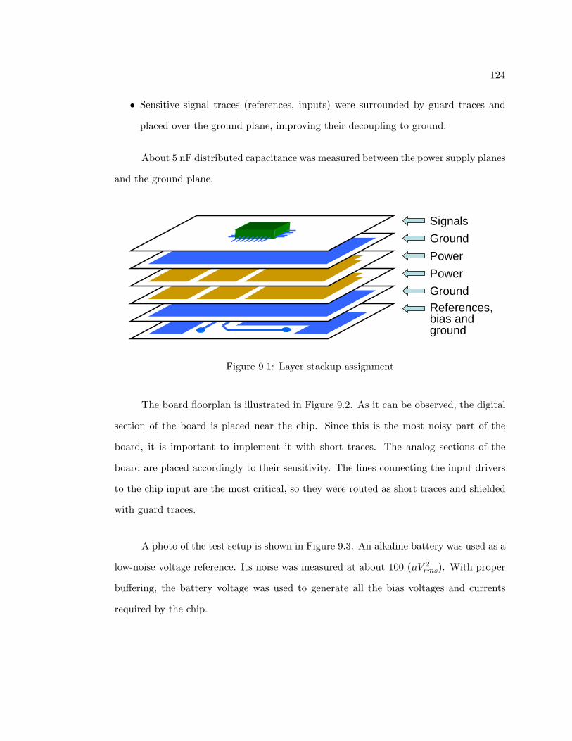
124
• Sensitive signal traces (references, inputs) were surrounded by guard traces and
placed over the ground plane, improving their decoupling to ground.
About 5 nF distributed capacitance was measured between the power supply planes
and the ground plane.
Signals
Ground
Power
Power
GroundReferences, bias and ground
Figure 9.1: Layer stackup assignment
The board floorplan is illustrated in Figure 9.2. As it can be observed, the digital
section of the board is placed near the chip. Since this is the most noisy part of the
board, it is important to implement it with short traces. The analog sections of the
board are placed accordingly to their sensitivity. The lines connecting the input drivers
to the chip input are the most critical, so they were routed as short traces and shielded
with guard traces.
A photo of the test setup is shown in Figure 9.3. An alkaline battery was used as a
low-noise voltage reference. Its noise was measured at about 100 (µV 2rms). With proper
buffering, the battery voltage was used to generate all the bias voltages and currents
required by the chip.
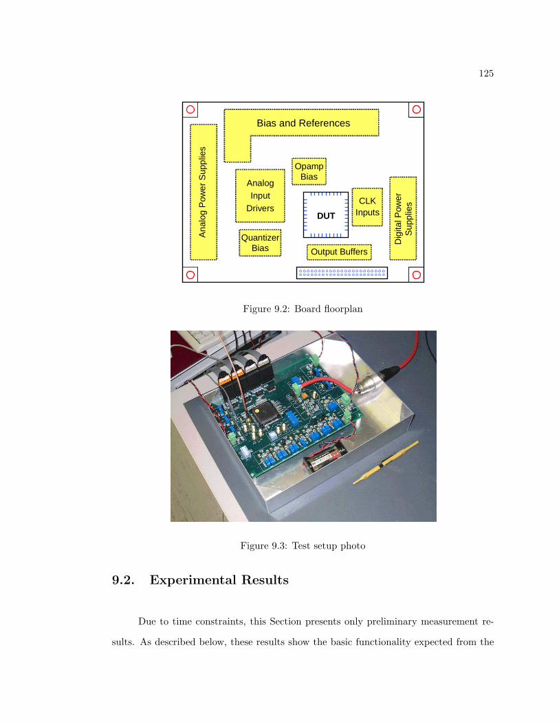
125
DUT
CLK Inputs
Dig
ital P
ower
S
uppl
ies
Ana
log
Pow
er S
uppl
ies
Bias and References
Output Buffers
Analog Input
Drivers
Quantizer Bias
Opamp Bias
Figure 9.2: Board floorplan
Figure 9.3: Test setup photo
9.2. Experimental Results
Due to time constraints, this Section presents only preliminary measurement re-
sults. As described below, these results show the basic functionality expected from the
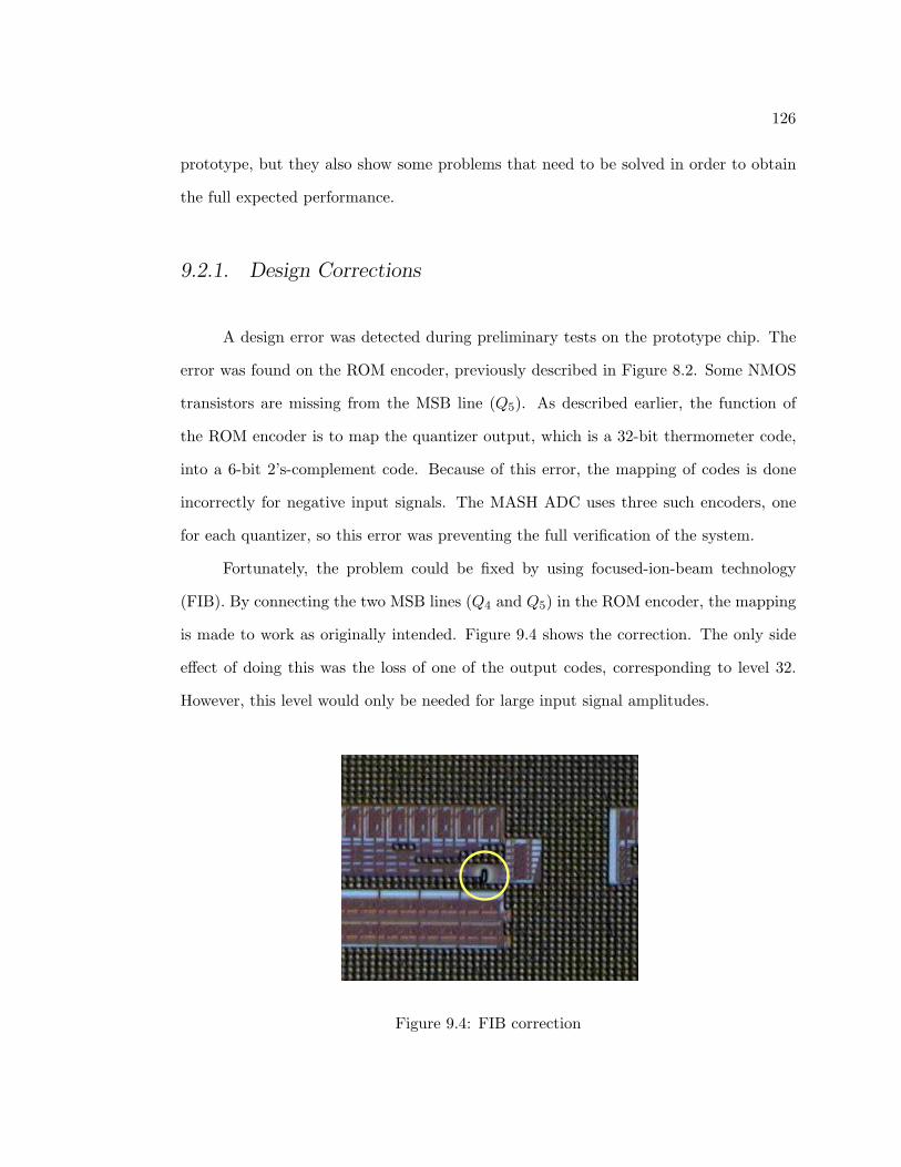
126
prototype, but they also show some problems that need to be solved in order to obtain
the full expected performance.
9.2.1. Design Corrections
A design error was detected during preliminary tests on the prototype chip. The
error was found on the ROM encoder, previously described in Figure 8.2. Some NMOS
transistors are missing from the MSB line (Q5). As described earlier, the function of
the ROM encoder is to map the quantizer output, which is a 32-bit thermometer code,
into a 6-bit 2’s-complement code. Because of this error, the mapping of codes is done
incorrectly for negative input signals. The MASH ADC uses three such encoders, one
for each quantizer, so this error was preventing the full verification of the system.
Fortunately, the problem could be fixed by using focused-ion-beam technology
(FIB). By connecting the two MSB lines (Q4 and Q5) in the ROM encoder, the mapping
is made to work as originally intended. Figure 9.4 shows the correction. The only side
effect of doing this was the loss of one of the output codes, corresponding to level 32.
However, this level would only be needed for large input signal amplitudes.
Figure 9.4: FIB correction

127
9.2.2. DAC error estimation and correction
The errors in the 32 unit elements in the first stage were estimated by correlating
the usage of each unit element with the MASH ADC output, as described in Section 4.3.
The 32-bit unit element vector was reconstructed in MATLAB from the output
of the first stage (V1) and from the begin pointer in the DWA block (Fig. 8.4). The
reconstruction process is done by simply selecting all unit elements between begin and
begin + V1. As explained in Section 8.7., it was possible to save several output pins by
obtaining the unit element vector from these two digital output signals.
During the measurements, the DWA algorithm was found to be somewhat ina-
dequate: In normal operation, with a sinusoidal input waveform, some of the DAC
element errors would not be properly estimated. A better scrambler must be used. To
make the DAC element usage sufficiently uniform for these measurements, a negative DC
input signal was applied to the modulator, forcing the DWA algorithm to select fewer
elements in each clock cycle. The estimated unit element errors for one of the chips are
shown in Figure 9.5. Note that each unit element is implemented as a pair of capacitors,
for fully-differential operation. Hence, the elements shown in the Figure represent the
errors for each pair of capacitors.
5 10 15 20 25 30
-3
-2.5
-2
-1.5
-1
-0.5
0
0.5
DAC Element
Err
or (
%F
S)
Figure 9.5: Estimated unit element errors
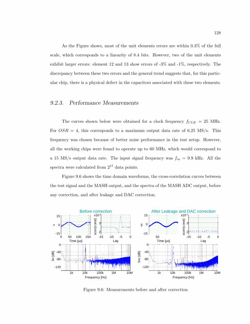
128
As the Figure shows, most of the unit elements errors are within 0.3% of the full
scale, which corresponds to a linearity of 8.4 bits. However, two of the unit elements
exhibit larger errors: element 12 and 13 show errors of -3% and -1%, respectively. The
discrepancy between these two errors and the general trend suggests that, for this partic-
ular chip, there is a physical defect in the capacitors associated with these two elements.
9.2.3. Performance Measurements
The curves shown below were obtained for a clock frequency fCLK = 25 MHz.
For OSR = 4, this corresponds to a maximum output data rate of 6.25 MS/s. This
frequency was chosen because of better noise performance in the test setup. However,
all the working chips were found to operate up to 60 MHz, which would correspond to
a 15 MS/s output data rate. The input signal frequency was fin = 9.9 kHz. All the
spectra were calculated from 217 data points.
Figure 9.6 shows the time domain waveforms, the cross-correlation curves between
the test signal and the MASH output, and the spectra of the MASH ADC output, before
any correction, and after leakage and DAC correction.
1k 10k 100k 1M 10MFrequency [Hz]
-120
-80
-40
0
-15
15
0
50 100 1500 -5-10 0-15Time [µs] Lag
Before correction
Sv
[dB
]v
xcor
rv,
test
2
3
x10-2
1k 10k 100k 1M 10MFrequency [Hz]
-15
15
0
50 100 1500 -5-10 0-15Time [µs] Lag
-120
-80
-40
0
After Leakage and DAC correction
Svc
[dB
]vc
xcor
rv,
test
2
3
x10-2
Figure 9.6: Measurements before and after correction

129
For the uncorrected output, the cross-correlation curve shows three terms standing
out from the others. They clearly indicate that there is quantization noise leakage
between the first and second stage, confirmed by the high noise floor observable in the
output spectrum.
The FIR coefficients were updated accordingly to the correlation terms, and the
estimated DAC errors shown in Figure 9.5 were also used to correct the output. The
resulting output shows the correlation terms now in line with the others, and the output
spectrum shows considerable improvements. Most of the harmonics were reduced, and
the noise floor was lowered by about 20 dB.
For a more clear view of the improvement, Figure 9.7 overlays the output spectra
without correction, after leakage correction, and after DAC error correction. The differ-
ence between the noise floor and harmonics is clearly significant. The DAC correction
seems to provide only a modest improvement in the noise floor.
Frequency [Hz]
Out
put S
pect
rum
[dB
]
0
-20
-40
-60
-80
-100
-120
-1401k 10k 100k 1M 10M
Before correctionAfter leakage correctionAfter DAC correction
Figure 9.7: Spectra of the non-corrected and corrected outputs
130
Although the above measurements show that the digital correction techniques are
functional, the attained performance is far from what was expected. Although the noise
floor was improved by 20 dB, it is still too high. In addition, many of the harmonic
components were not sufficiently reduced, further degrading performance. Due to these
effects, the total in-band noise is essentially unchanged.
Two problems were identified which may explain these performance degradations:
• One of the problems is related with the passive adder in the modulator stages.
As explained in Section 7.4.1., the passive adder introduces an attenuation factor
before the quantizer. This means that any non-ideal effects after the passive adder
(such as quantizer offsets) become larger when referred to its inputs. This effect was
observed in the measurement results. It causes a reduction in the dynamic range
of the MASH ADC, but there is a more important implication: The output signal
in the opamp preceding the passive adder is forced to operate in a region where its
gain is less linear. The resulting increased distortion modulates the quantization
noise, creating a higher noise floor.
• The second problem is related with input signal distortion. Many of the harmonics
shown in the output spectrum were found to be present at the negative input pin
of the prototype (but not at the positive pin). They appeared there even when
the circuit was not in operation. This is more intriguing since the positive and
negative input pins use a similar front-end circuit. At the time of this writing, the
reason for this problem had not yet been determined.
The passive adder input referred sensitivity problem indicates that it is preferable
to implement the addition of feedforward paths with active circuitry. This would have
some other additional benefits: The adjustment of quantizer thresholds (to compensate
for the attenuation factor) would no longer be needed, and the quantizer’s linearity
requirements would be easier to meet, since the quantization steps would be larger.

131
9.2.4. Power Consumption
The measured power consumption is shown in Table 9.1, for a power supply of 1.8 V
and a clock frequency of 20 MHz. For other clock frequencies, the power consumption of
the digital section scales with the clock frequency, while the power consumption of the
analog section remains roughly the same. The measured values agree with the expected
power consumption for this design. The total of 97.7 mW is considerably lower than
other published MASH ADC architectures.
Table 9.1: Power consumption in mW
Opamps 50.8
Quantizers 37.3
Switch drivers 1.5
Digital section 1.1
Clock generator 7.0
Total 97.7
132
CHAPTER 10. CONCLUSIONS
10.1. Conclusions
In this dissertation, the following topics associated with high-performance ∆Σ
analog-to-digital conversion where studied in detail:
• The trade-offs of extending bandwidth without losing accuracy in ∆Σ ADCs were
described.
• It was shown that traditional implementations — using ∆Σ modulators with
conventional signal transfer functions, multi-stage architectures and conventional
multi-bit DAC linearization techniques — require high-quality analog circuit com-
ponents to meet their high-accuracy specifications.
• Three techniques were presented which can significantly relax analog circuit re-
quirements. They achieve this by using digital techniques to estimate and correct
analog circuit imperfections (adaptive leakage compensation and DAC error esti-
mation and correction), and by preventing critical signals from being processed by
non-ideal components (low-distortion ∆Σ topologies). These techniques were im-
proved in the proposed research, and combined in a MASH ADC architecture which
does not require high-quality analog circuit components to achieve and maintain
high-resolution and wide bandwidth of operation.
• A prototype chip combining the described techniques was designed and fabricated.
Although the preliminary test results show basic functionality and higher band-
width of operation, the accuracy is limited by high noise floor and harmonics.

133
10.2. Future Work
The estimation algorithms described in this thesis are based on the correlation
between signals which can contain significant disturbances. The speed and accuracy of
the leakage compensation process and DAC error estimation process are affected by the
input signal and by the quantization noise. These algorithms can be improved by:
• High-pass filtering of the output signal. This would suppress input signal compo-
nents, allowing the correlation to be more accurate.
• Employing architectures which remove the input signal from the output without
requiring filtering.
In addition, a dynamic adaptation step size can be used. A large adaptation step
size can be used initially to speed up the convergence of adaptive filter coefficients. After
the adaptation is complete, a small step size can be used to keep track of any long-term
process variations, with low adaptation noise.
Finally, the DAC error estimation and correction was so far only implemented off-
line, by post-processing relevant data in MATLAB. It would be interesting to implement
the DAC error estimation and correction on a prototype chip.
134
Bibliography
[1] “Very-high-speed digital subscriber lines,” System Requirements Document(T1E1.4/98-043R3) American National Standards Institute, 1998.
[2] K. Zangi and R. Koilpillai, “Software radio issues in cellular base stations,” IEEEJournal on Selected Areas in Communications, vol. 17, no. 4, pp. 561–573, April1999.
[3] A. Salkintzis, H. Nie, and P. Mathiopoulos, “ADC and DSP challenges in thedevelopment of software radio base stations,” IEEE Personal Communications,vol. 6, no. 4, pp. 47–55, August 1999.
[4] A. Karanicolas, H. Lee, and K. Bacrania, “A 15-b 1-Msamples/s digitally self-calibrated pipeline ADC,” IEEE Journal of Solid-State Circuits, vol. 28, no. 12,pp. 1207–1215, December 1993.
[5] D. Mercer, “A 14-b 2.5 MSPS pipelined ADC with on-chip EPROM,” IEEEJournal of Solid-State Circuits, vol. 31, no. 1, pp. 70–76, January 1996.
[6] O. Erdogan, P. Hurst, and S. Lewis, “A 12-b digital-background-calibrated algo-rithmic ADC with -90-dB THD,” IEEE Journal of Solid-State Circuits, vol. 34,no. 12, pp. 1812–1820, December 1999.
[7] B. Murmann and B. Boser, “A 12-bit 75-MS/s pipelined ADC using open-loopresidue amplification,” IEEE Journal of Solid-State Circuits, vol. 38, no. 12, pp.2040–2050, December 2003.
[8] E. Siragusa and I. Galton, “A digitally enhanced 1.8V 15b 40MS/s CMOS pipelinedADC,” in IEEE International Solid-State Circuits Conference, Digest of TechnicalPapers, February 2004, pp. 450–451.
[9] P. Benabes, A. Gauthier, and D. Billet, “New wideband sigma-delta convertor,”IEE Electronics Letters, vol. 29, no. 17, pp. 1575–1577, August 1993.
[10] Jesper Steensgaard-Madsen, High-Performance Data Converters, Ph.D. thesis,The Technical University of Denmark, Department of Information Technology,March 8, 1999.
[11] J. Silva, U. Moon, J. Steensgaard, and G. C. Temes, “Wideband low-distortiondelta-sigma ADC topology,” IEE Electronics Letters, vol. 37, no. 12, pp. 737–738,June 2001.
[12] A. Wiesbauer and G. C. Temes, “Adaptive compensation of analog circuit im-perfections for cascaded sigma-delta modulators,” in Proceedings of the Asilomar
135
Conference on Circuits, Systems and Computers, November 1996, vol. 2, pp. 1073–1077.
[13] A. Wiesbauer and G. C. Temes, “On-line digital compensation of analog circuitimperfections for cascaded delta-sigma modulators,” in Proceedings of the IEEE-CAS Workshop on Analog and Mixed IC Design, September 1996, pp. 92–97.
[14] Peter Kiss, Adaptive Digital Compensation of Analog Circuit Imperfections forCascaded Delta-Sigma Analog-to-Digital Converters, Ph.D. thesis, “Politehnica”University of Timisoara, Romania, August 20, 1999.
[15] X. Wang, U. Moon, M. Liu, and G. C. Temes, “Digital correlation technique forthe estimation and correction of DAC errors in multibit MASH ∆Σ ADCs,” inProceedings of the IEEE International Symposium on Circuits and Systems, May2002, vol. 4, pp. IV–691–IV–694.
[16] J. Silva, X. Wang, P. Kiss, U. Moon, and G. C. Temes, “Digital techniques forimproved ∆Σ data conversion,” in Proceedings of the IEEE Costum IntegratedCircuits Conference, May 2002, pp. 183–190.
[17] Xuesheng Wang, Fully Digital Technique for the Estimation and Correction of theDAC Error in Multi-Bit Delta Sigma ADCs, Ph.D. thesis, Oregon State University,School of Electrical Engineering and Computer Science, December 1, 2003.
[18] S. R. Norsworthy, R. Schreier, and G. C. Temes, Eds., Delta-Sigma Data Convert-ers: Theory, Design, and Simulation, New York: IEEE Press, 1996.
[19] E. Hogenauer, “An economical class of digital filters for decimation and interpo-lation,” IEEE Transactions on Acoustics, Speech, and Signal Processing, vol. 29,no. 2, pp. 155–162, April 1981.
[20] E. Lee and D. Messerschmitt, Digital Communication, Boston: Kluwer AcademicPublishers, 1994.
[21] K. Chao, S. Nadeem, W. Lee, and C. Sodini, “A higher order topology for in-terpolative modulators for oversampling A/D conversion,” IEEE Transactions onCircuits and Systems, vol. 37, no. 3, pp. 309–318, March 1990.
[22] S. Jantzi, K. Martin, and A. Sedra, “Quadrature bandpass ∆Σ modulation fordigital radio,” IEEE Journal of Solid-State Circuits, vol. 32, no. 12, pp. 1935–1950, December 1997.
[23] L. Carley and J. Kenney, “A 16-bit 4th order noise-shaping D/A converter,” inProceedings of the IEEE Costum Integrated Circuits Conference, May 1988, pp.21.7/1–21.7/4.
[24] L. Carley, “A noise-shaping coder topology for 15+ bit converters,” IEEE Journalof Solid-State Circuits, vol. 24, no. 2, pp. 267–273, April 1989.
136
[25] B. Leung and S. Sutarja, “Multi-bit Σ∆ A/D converters incorporating a novelclass of dynamic element matching techniques,” IEEE Transactions on Circuitsand Systems–II: Analog and Digital Signal Processing, vol. 39, pp. 35–51, January1992.
[26] R. Baird and T. Fiez, “Linearity enhancement of multibit ∆Σ A/D and D/Aconverters using data weighted averaging,” IEEE Transactions on Circuits andSystems–II: Analog and Digital Signal Processing, vol. 42, no. 12, pp. 753–762,December 1995.
[27] I. Galton, “Spectral shaping of circuit errors in digital-to-analog converters,” IEEETransactions on Circuits and Systems–II: Analog and Digital Signal Processing, vol.44, no. 10, pp. 808–817, October 1997.
[28] T. Brooks, D. Robertson, D. Kelly, A. Del Muro, and S. Harston, “A cascadedsigma-delta pipeline A/D converter with 1.25 MHz signal bandwidth and 89 dBSNR,” IEEE Journal of Solid-State Circuits, vol. 32, no. 12, pp. 1896–1906, De-cember 1997.
[29] A. Marques, V. Peluso, M. Steyaert, and W. Sansen, “A 15-b resolution 2-MHznyquist rate ∆Σ ADC in a 1-µm CMOS technology,” IEEE Journal of Solid-StateCircuits, vol. 33, no. 7, pp. 1065–1075, July 1998.
[30] I. Fujimori, L. Longo, A. Hairapetian, K. Seiyama, S. Kosic, J. Cao, and S. Chan,“A 90-dB SNR 2.5-MHz output-rate ADC using cascaded multibit delta-sigmamodulation at 8x oversampling,” IEEE Journal of Solid-State Circuits, vol. 35, no.12, pp. 1820–1828, December 2000.
[31] K. Vleugels, S. Rabii, and B. Wooley, “A 2.5 v sigma-delta modulator for broad-band communications applications,” IEEE Journal of Solid-State Circuits, vol. 36,no. 12, pp. 1887–1899, December 2001.
[32] Y. Park, S. Karthikeyan, W. Woe, Z. Jiang, and T. Tan, “A 16-bit, 5 MHz multi-bit sigma-delta ADC using adaptively randomized DWA,” in Proceedings of theIEEE Costum Integrated Circuits Conference, September 2003, pp. 115–118.
[33] A. Hamoui and K. Martin, “A 1.8-V 3-MS/s 13-bit ∆Σ A/D converter withpseudo data-weighted-averaging in 0.18-µm digital cmos,” in Proceedings of theIEEE Costum Integrated Circuits Conference, September 2003, pp. 119–122.
[34] P. Balmelli and Q. Huang, “A 25MS/s 14b 200 mW Σ∆ modulator in 0.18 µmCMOS,” in IEEE International Solid-State Circuits Conference, Digest of Techni-cal Papers, February 2004, vol. 1, pp. 74–75.
[35] S. Haykin, Adaptive Filter Theory, Englewood Cliffs, New York: Prentice Hall,1991.
137
[36] I. Balasingham, S. Mitra, and T. Ramstad, “Adaptive filters based on tappedcascaded allpass sections,” in Proc. of the Norwegian Signal Processing Symposiumand Workshop, May 1997, pp. 113–118.
[37] W. Ki and G. C. Temes, “Offset-compensated switched-capacitor integrators,” inProceedings of the IEEE International Symposium on Circuits and Systems, vol. 4.
[38] D. A. Johns and K. Martin, Analog Integrated Circuit Design, John Wiley & Sons,1997.
[39] R. Schreier and G. C. Temes, Understanding Delta-Sigma Data Converters, toappear, Wiley - IEEE Press, 2004, Appendix C.
[40] C. Enz and G. C. Temes, “Circuit techniques for reducing the effects of op-amp im-perfections: Autozeroing, correlated double sampling, and chopper stabilization,”PIEEE, vol. 84, no. 11, pp. 1584–1614, November 1996.
[41] M. Dessouky and A. Kaiser, “Very low-voltage digital-audio ∆Σ modulator with88-dB dynamic range using local switch bootstrapping,” IEEE Journal of Solid-State Circuits, vol. 36, no. 3, pp. 349–355, March 2001.
[42] T. Choi, R. Kaneshiro, R. Brodersen, P. Gray, W. Jett, and M. Wilcox, “High-frequency CMOS switched-capacitor filters for communications application,” IEEEJournal of Solid-State Circuits, vol. 18, no. 6, pp. 652–664, December 1983.
[43] P. Hurst and S. Lewis, “Determination of stability using return ratios in balancedfully differential feedback circuits,” IEEE Transactions on Circuits and Systems,vol. 42, no. 12, pp. 805–817, December 1995.
[44] B. Razavi and B. Wooley, “Design techniques for high-speed, high-resolution com-parators,” IEEE Journal of Solid-State Circuits, vol. 27, no. 12, pp. 1916–1926,December 1992.
[45] I. Mehr and D. Dalton, “A 500-MSamples, 6-bit nyquist-rate ADC for disk-driveread-channel applications,” IEEE Journal of Solid-State Circuits, vol. 34, no. 7,pp. 912–920, July 1999.
[46] J. Rabaey, Digital Integrated Circuits: A Design Perspective, New Jersey: PrenticeHall, 1996.
[47] L. Dorrer, F. Kuttner, A. Wiesbauer, A. Giandomenico, and T. Hartig, “10-bit,3mW continuous-time sigma-delta ADC for UMTS in a 0.12µm CMOS process,”in European Solid-State Circuits Conference, September 2003.
[48] C. Baugh and B. Wooley, “A two’s complement parallel array multiplication al-gorithm,” IEEE Transactions on Computers, vol. C-22, no. 12, pp. 1045–1047,December 1973.

138
[49] M. I. Montrose, Ed., Printed Circuit Board Design Techniques for EMC Compli-ance, John Wiley & Sons, 2000.