high-index-contrast ridge waveguide lasers fabricated … · high-index-contrast ridge waveguide...
TRANSCRIPT

High-Index-Contrast Ridge Waveguide Lasers Fabricated Via Oxygen-Enhanced Wet Thermal Oxidation
Di Liang*a, Jusong Wang a, Douglas C. Hall a, Gregory M. Peake,b Quesnell Hartmannc
aDept. of Electrical Engineering, Univ. of Notre Dame, Notre Dame, IN USA 46556-5637; bSandia National Laboratory, Albuquerque, NM USA 87185
cEpiworks, Inc.,Champaign, IL USA 61822
ABSTRACT A simple, novel self-aligned deep etch plus wet thermal oxidization process is demonstrated which enables high-index-contrast (HIC) ridge waveguide (RWG) lasers fabricated in a high-efficiency, high-power AlGaAs/InAlGaAs/GaAs graded-index separate confinement heterostructure to operate with a curved half-ring resonator geometry having a bend radius as low as 10 µm. A wet thermal oxidation process modified through addition of <1% O2 to the N2 carrier gas is shown to smooth the sidewall roughness of etched AlGaAs ridge structures 10-100 fold as the oxidation front progresses inward. The reduction of propagation scattering loss due to the reduced sidewall roughness is examined. The thermal oxide grown on the deeply-etched RWG sidewalls and base also provides electrical isolation from the contact metallization, resulting in a simplified, self-aligned process, and yields a RWG structure which effectively prevents current spreading. The thermal oxide appears to be of sufficiently high quality to passivate the etched active region surface based on a comparative analysis of straight RWG lasers of varying stripe widths (w=5 to 150 µm) passivated with native-oxide vs. PECVD-deposited SiO2. For example, at w<15 µm, the SiO2-insulated devices have ~2X higher threshold current densities than the native-oxide devices for comparable bar lengths. The resulting high lateral optical confinement factor at the semiconductor/oxide interface (Δn=1.69) significantly enhances the laser gain and efficiency. A native-oxide-defined straight laser (w=7 µm, L= 452 µm) operates cw (300 K, unbonded, p-side up) with a threshold current of Ith=21.5 mA (Jth=679.5 A/cm2) and slope efficiency of 1.19 A/W (differential quantum efficiency = 78%) at a wavelength of ~813 nm. Keywords: high-index-contrast, ridge waveguide laser, thermal oxidation, oxidation smoothing, half-ring resonator, surface passivation
1. INTRODUCTION Reminiscent of the historical evolution of microelectronic integrated circuits, photonic integrated circuits (PICs) are now further evolving through a new emphasis on shrinking device size, increased functionality and cost reduction. The attention to these critical concerns has recently led to a new focus on the more fundamental components, such as waveguides and diode lasers. As a key parameter in all of guided wave theory, the core-cladding index contrast (∆n) presents a promising research avenue for new breakthroughs. High-index contrast (HIC) devices with ∆n >1 may allow a simultaneous growth of device density and integration complexity within the same basic set of materials and fabrication processes. With the smaller PIC footprint and large free spectral range resonators they enable, HIC photonic devices may soon play a leading role in numerous applications. The success of HIC passive waveguide devices made on silicon-on-insulator (SOI) substrates[1] naturally leads one to consider extension to the III-V semiconductors, the dominant materials for most active optoelectronic devices. Due to the low refraction index of dielectrics (n~1.5-2), both native oxides and chemical vapor deposition (CVD) dielectrics can offer a large index contrast semiconductor/dielectric interface. A III-V compound semiconductor wet-thermal oxidation process[2] for achieving a high-quality thermal oxide on AlxGa1-xAs with high Al composition offers one approach for realizing an HIC interface. Conventionally, this wet oxidation process has only been suited to the selective oxidization of high Al composition AlxGa1-xAs (1<x<0.6) materials. Through a modification to the conventional wet oxidation process introduced at the University of Notre Dame, in which trace amounts of O2 [0-10000 ppm (1%) relative to N2] are added to the process gas stream (N2+H2O vapor), significantly enhanced oxidation rates for low Al-ratio AlxGa1-xAs and reduced oxidation rate selectivity to Al content have been achieved.[3] Low Al-ratio AlGaAs waveguide core regions, therefore, can now be oxidized laterally through this O2-enhanced wet thermal oxidation technique without fully oxidizing the higher Al-ratio cladding layer, allowing a much higher, real lateral index
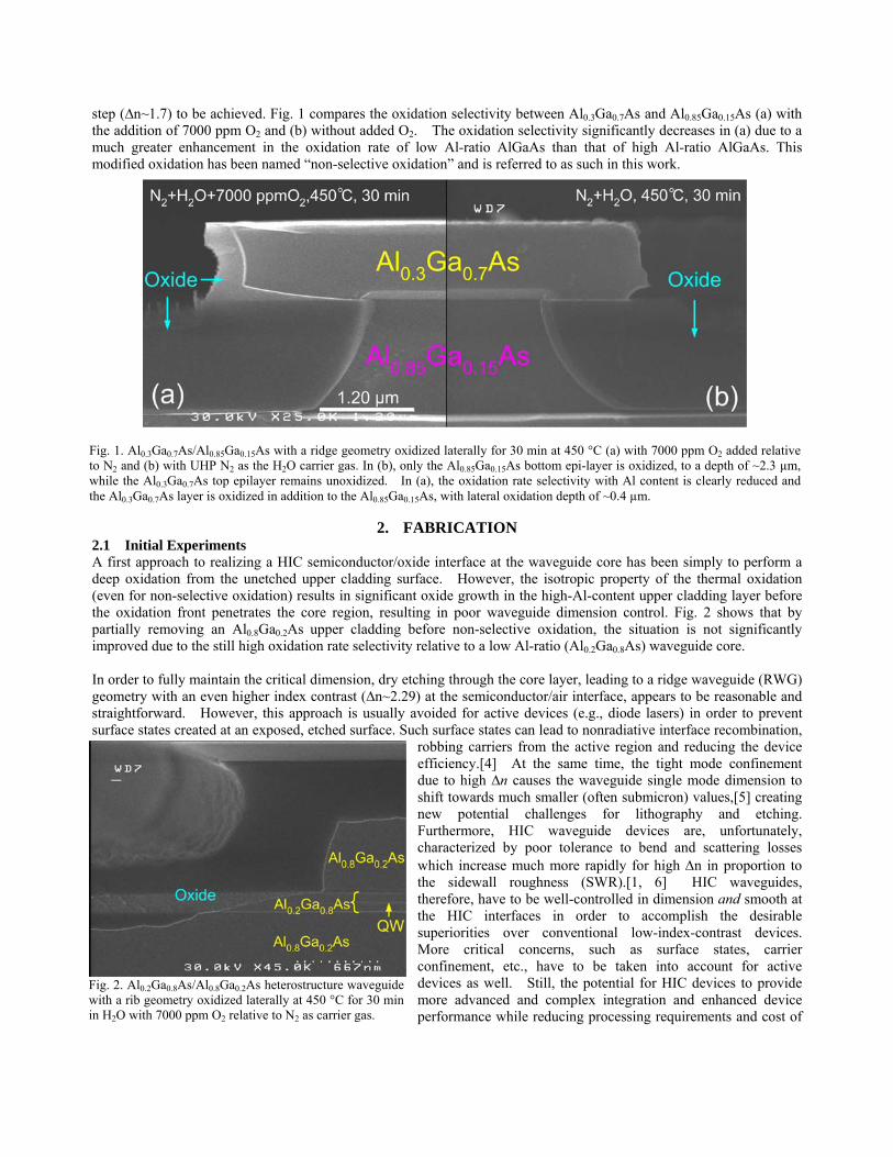
step (∆n~1.7) to be achieved. Fig. 1 compares the oxidation selectivity between Al0.3Ga0.7As and Al0.85Ga0.15As (a) with the addition of 7000 ppm O2 and (b) without added O2. The oxidation selectivity significantly decreases in (a) due to a much greater enhancement in the oxidation rate of low Al-ratio AlGaAs than that of high Al-ratio AlGaAs. This modified oxidation has been named “non-selective oxidation” and is referred to as such in this work.
Fig. 1. Al0.3Ga0.7As/Al0.85Ga0.15As with a ridge geometry oxidized laterally for 30 min at 450 °C (a) with 7000 ppm O2 added relative to N2 and (b) with UHP N2 as the H2O carrier gas. In (b), only the Al0.85Ga0.15As bottom epi-layer is oxidized, to a depth of ~2.3 µm, while the Al0.3Ga0.7As top epilayer remains unoxidized. In (a), the oxidation rate selectivity with Al content is clearly reduced and the Al0.3Ga0.7As layer is oxidized in addition to the Al0.85Ga0.15As, with lateral oxidation depth of ~0.4 µm.
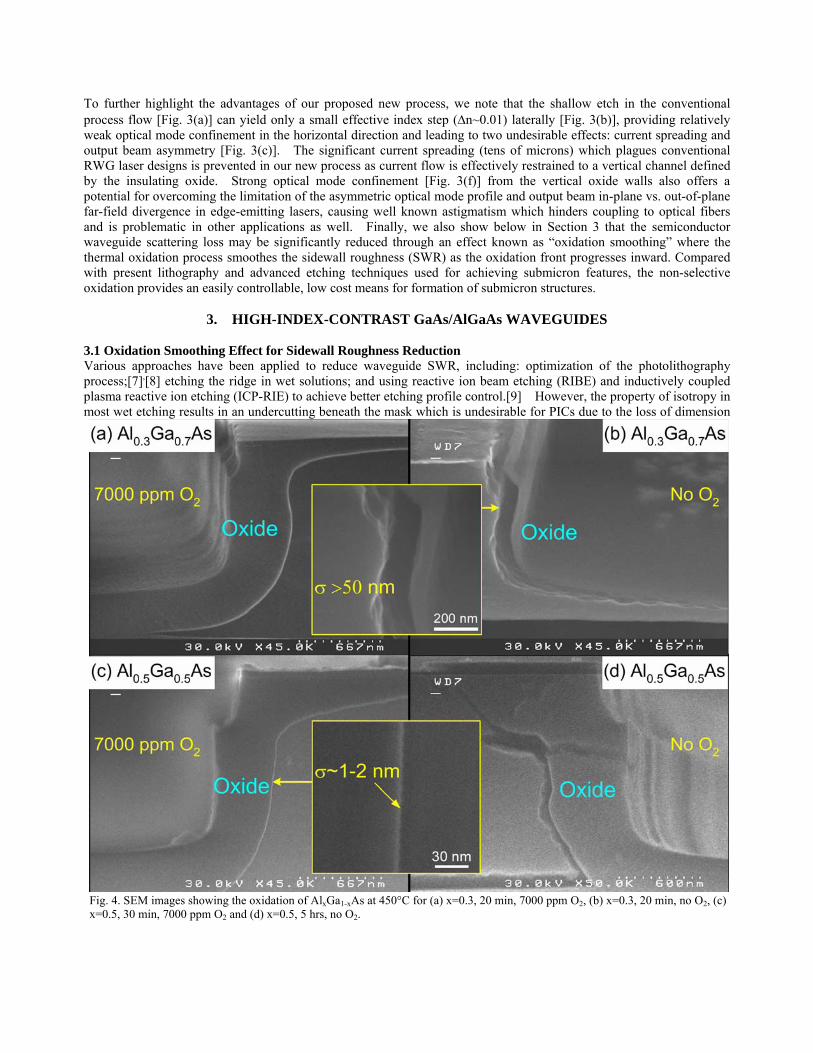
2. FABRICATION 2.1 Initial Experiments A first approach to realizing a HIC semiconductor/oxide interface at the waveguide core has been simply to perform a deep oxidation from the unetched upper cladding surface. However, the isotropic property of the thermal oxidation (even for non-selective oxidation) results in significant oxide growth in the high-Al-content upper cladding layer before the oxidation front penetrates the core region, resulting in poor waveguide dimension control. Fig. 2 shows that by partially removing an Al0.8Ga0.2As upper cladding before non-selective oxidation, the situation is not significantly improved due to the still high oxidation rate selectivity relative to a low Al-ratio (Al0.2Ga0.8As) waveguide core. In order to fully maintain the critical dimension, dry etching through the core layer, leading to a ridge waveguide (RWG) geometry with an even higher index contrast (∆n~2.29) at the semiconductor/air interface, appears to be reasonable and straightforward. However, this approach is usually avoided for active devices (e.g., diode lasers) in order to prevent surface states created at an exposed, etched surface. Such surface states can lead to nonradiative interface recombination,
robbing carriers from the active region and reducing the device efficiency.[4] At the same time, the tight mode confinement due to high ∆n causes the waveguide single mode dimension to shift towards much smaller (often submicron) values,[5] creating new potential challenges for lithography and etching. Furthermore, HIC waveguide devices are, unfortunately, characterized by poor tolerance to bend and scattering losses which increase much more rapidly for high Δn in proportion to the sidewall roughness (SWR).[1, 6] HIC waveguides, therefore, have to be well-controlled in dimension and smooth at the HIC interfaces in order to accomplish the desirable superiorities over conventional low-index-contrast devices. More critical concerns, such as surface states, carrier confinement, etc., have to be taken into account for active devices as well. Still, the potential for HIC devices to provide more advanced and complex integration and enhanced device performance while reducing processing requirements and cost of
Fig. 2. Al0.2Ga0.8As/Al0.8Ga0.2As heterostructure waveguide with a rib geometry oxidized laterally at 450 °C for 30 min in H2O with 7000 ppm O2 relative to N2 as carrier gas.

III-V semiconductor PICs, a primary concern for PIC industry, motivates substantial current research in this area. 2.2 Fabrication Procedures We have developed a simple, novel self-aligned deeply-etched plus wet thermally oxidized GaAs-based RWG laser fabrication process for high-performance low-cost passive and active HIC devices fabricated by commonly available microelectronics manufacturing facilities. Fig. 3 compares the process flow for fabrication of conventional vs. proposed oxide-defined HIC RWG lasers. The fabrication of passive waveguides is largely identical to the laser fabrication shown except that additional current confinement and metallization issues need be taken into account. Laser fabrication typically starts with a ~200 nm plasma-enhanced chemical vapor deposition (PECVD) SiNx deposition to protect the p+-GaAs cap layer from later oxidation. The waveguide stripe is then patterned through conventional photolithography followed by two successive dry etching steps to translate the photoresist (PR) pattern to the SiNx layer and semiconductor epilayers, forming a ridge as shown in Fig. 3(d). Unlike the conventional dry etching stopped above the active layer [Fig. 3(a)] to keep defects introduced by etching away from the active region, dry etching in this case reaches the lower cladding layer in order to keep the waveguide lateral dimension equal to that of the PR mask. Nonradiative recombination due to defects formed during this initial etching process is largely reduced during the following non-selective oxidation. The oxide grown on the waveguide sidewalls (and base) [Fig. 3(e)] results in a HIC (∆n~1.7) semiconductor/oxide interface, enabling the realization of a HIC RWG capable of supporting very sharp bending, while simultaneously providing scaling from a conventional-lithography-defined ridge dimension (≥1 µm) to the submicron dimensions required for HIC waveguide single-mode operation. Furthermore, instead of depositing PECVD SiO2 or SiNx for electrical confinement and surface passivation [Fig. 3(b)], the native oxide itself acts directly as the dielectric layer, providing a self-aligned process which eliminates the potential alignment errors and the narrowing of the top contact area [shown by two “d”s in Fig. 3(c)] unavoidably resulting from a second “current-window open” lithography step in a conventional fabrication process flow. In our new process, a final dry etching procedure then selectively removes the dielectric stripe mask, using special care to prevent etch damage to the p+-GaAs cap layer, and the wafer is then thinned, metallized and cleaved into laser bars.
Fig. 3. Fabrication process of conventional and non-selective oxidation defined HIC RWG Lasers.
To further highlight the advantages of our proposed new process, we note that the shallow etch in the conventional process flow [Fig. 3(a)] can yield only a small effective index step (Δn~0.01) laterally [Fig. 3(b)], providing relatively weak optical mode confinement in the horizontal direction and leading to two undesirable effects: current spreading and output beam asymmetry [Fig. 3(c)]. The significant current spreading (tens of microns) which plagues conventional RWG laser designs is prevented in our new process as current flow is effectively restrained to a vertical channel defined by the insulating oxide. Strong optical mode confinement [Fig. 3(f)] from the vertical oxide walls also offers a potential for overcoming the limitation of the asymmetric optical mode profile and output beam in-plane vs. out-of-plane far-field divergence in edge-emitting lasers, causing well known astigmatism which hinders coupling to optical fibers and is problematic in other applications as well. Finally, we also show below in Section 3 that the semiconductor waveguide scattering loss may be significantly reduced through an effect known as “oxidation smoothing” where the thermal oxidation process smoothes the sidewall roughness (SWR) as the oxidation front progresses inward. Compared with present lithography and advanced etching techniques used for achieving submicron features, the non-selective oxidation provides an easily controllable, low cost means for formation of submicron structures.
3. HIGH-INDEX-CONTRAST GaAs/AlGaAs WAVEGUIDES 3.1 Oxidation Smoothing Effect for Sidewall Roughness Reduction Various approaches have been applied to reduce waveguide SWR, including: optimization of the photolithography process;[7],[8] etching the ridge in wet solutions; and using reactive ion beam etching (RIBE) and inductively coupled plasma reactive ion etching (ICP-RIE) to achieve better etching profile control.[9] However, the property of isotropy in most wet etching results in an undercutting beneath the mask which is undesirable for PICs due to the loss of dimension
Fig. 4. SEM images showing the oxidation of AlxGa1-xAs at 450°C for (a) x=0.3, 20 min, 7000 ppm O2, (b) x=0.3, 20 min, no O2, (c) x=0.5, 30 min, 7000 ppm O2 and (d) x=0.5, 5 hrs, no O2.
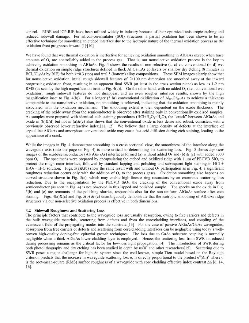
control. RIBE and ICP-RIE have been utilized widely in industry because of their optimized anisotropic etching and reduced sidewall damage. For silicon-on-insulator (SOI) structures, a partial oxidation has been shown to be an effective technique for smoothing an etched interface due to the isotropic nature of the thermal oxidation process as the oxidation front progresses inward.[1],[10] We have found that wet thermal oxidation is ineffective for achieving oxidation smoothing in AlGaAs except when trace amounts of O2 are controllably added to the process gas. That is, our nonselective oxidation process is the key to achieving oxidation smoothing in AlGaAs. Fig. 4 shows the results of non-selective (a, c) vs. conventional (b, d) wet thermal oxidation on simple ridge structures defined in thick AlxGa1-xAs epilayers by shallow dry etching (8 minutes in BCl3/Cl2/Ar by RIE) for both x=0.3 (top) and x=0.5 (bottom) alloy compositions. These SEM images clearly show that for nonselective oxidation, initial rough sidewall features of ≥100 nm dimension are smoothed away at the inward progressing oxidation front, resulting in an apparent final SWR (at least in the cross section plane) as low as 1-2 nm RMS (as seen by the high magnification inset to Fig. 4(c)). On the other hand, with no added O2 (i.e., conventional wet oxidation), rough sidewall features do not disappear, and an even rougher interface results, shown by the high magnification inset to Fig. 4(b)). For a longer (5 hr) conventional oxidization of Al0.5Ga0.5As to achieve a thickness comparable to the nonselective oxidation, no smoothing is achieved, indicating that the oxidation smoothing is mainly associated with the oxidation mechanism. The smoothing extent is then dependent on the oxide thickness. The cracking of the oxide away from the semiconductor is observed after staining only in conventionally oxidized samples. As samples were prepared with identical etch staining procedures (HCl+H2O2+H2O), the “crack” between AlGaAs and oxide in (b)&(d) but not in (a)&(c) also shows that the conventional oxide is less dense and robust, consistent with a previously observed lower refractive index.[11, 12] We believe that a large density of defects at the interface of crystalline AlGaAs and amorphous conventional oxide may cause fast acid diffusion during etch staining, leading to the appearance of a crack.
While the images in Fig. 4 demonstrate smoothing in a cross sectional view, the smoothness of the interface along the waveguide axis (into the page on Fig. 4) is more critical to determining the scattering loss. Fig. 5 shows top view images of the oxide/semiconductor (Al0.3Ga0.7As) interfaces formed (a) without added O2 and (b) & (c) with added 7000 ppm O2. The specimens were prepared by encapsulating the etched and oxidized ridge with 1 μm of PECVD SiO2 to protect the rough outer interface, followed by standard lapping and polishing and subsequent light staining in HCl + H2O2 + H2O solution. Figs. 5(a)&(b) show the same result with and without O2 participation as in Fig. 4: a significant roughness reduction occurs only with the addition of O2 to the process gases. Oxidation smoothing also happens on curved structure shown in Fig. 5(c), which may enable high-finesse ring resonators by an enormous scattering loss reduction. Due to the encapsulation by the PECVD SiO2, the cracking of the conventional oxide away from semiconductor (as seen in Fig. 4) is not observed in this lapped and polished sample. The specks on the oxide in Fig. 5(b) and (c) are remnants of the polishing slurries, responsible also for the non-uniform AlGaAs surface after etch staining. Figs. 4(a)&(c) and Fig. 5(b) & (c) unambiguously demonstrate that the isotropic smoothing of AlGaAs ridge structures via our non-selective oxidation process is effective in both dimensions. 3.2 Sidewall Roughness and Scattering Loss The principle factors that contribute to the waveguide loss are usually absorption, owing to free carriers and defects in the bulk waveguide materials, scattering from defects and from the core/cladding interfaces, and coupling of the evanescent field of the propagating modes into the substrate.[13] For the case of passive AlGaAs/GaAs waveguides, absorption from free carriers or defects and scattering from core/cladding interfaces can be negligible using today’s well-proven high-quality doping-free epitaxial growth techniques. The loss due to GaAs substrate coupling is normally negligible when a thick AlGaAs lower cladding layer is employed. Hence, the scattering loss from SWR introduced during processing remains as the critical factor for low-loss light propagation.[14] The introduction of SWR during both photolithography and dry etching has been studied in depth by us[8] and other researchers[15]. Scattering due to SWR poses a major challenge for high-∆n system since the well-known, simple Tien model based on the Rayleigh criterion predicts that the increase in waveguide scattering loss αs is directly proportional to the product σ2(∆n)2 where σ is the root-mean-square (RMS) surface roughness of a waveguide with core cladding effective index contrast ∆n [6, 14, 16].

More rigorous autocorrelation models accounting for spatial periodicities and the scattering roughness coherence length even predict that αs increases in proportional to (∆n)3.[1, 17, 18] With the device size shrinkage down to only an order of magnitude larger than that of the SWR, propagation loss due to the rough sidewalls can be substantial. Based on the Tien model, Fig. 6 (a) shows the dependence of scattering loss on RMS average SWR σ, for 3 ridge waveguide structures of different lateral index contrast: a conventional shallow-etched ridge with ∆n=0.1, a deeply-etched, air-clad ridge with ∆n=2.29, and our proposed oxide-confined ridge with ∆n=1.69. While an air-clad structure is not widely employed for active injection lasers for reasons discussed in Section 1, it has been used for passive AlGaAs/GaAs microring resonator devices which were fabricated using extensively optimized ICP-RIE or chemical-assisted ion beam etching (CAIBE) to achieve SWR in the 10-20 nm range.[19, 20] While 1-2 nm SWR can be achieved for InP-based alloys with optimized ICP-RIE,[21] the state-of-the-art in AlGaAs is not as low due to effects of high chemical reactivity of Al on the etching mechanism. SWR achieved in the Plasma-Therm 790 RIE tool used in this work is frequently in the 50-100 nm range, corresponding [Fig. 6 (a)] to αs range of 3-30 dB/cm for HIC RWGs (air-clad & oxide-clad), unacceptably high for many PIC applications. Comparing a σ=10 nm air-clad waveguide to a σ=1-2 nm SWR obtained by oxidation smoothing (see Fig. 4 & 5), it appears that the lowest achievable loss could be reduced from ~0.2 dB/cm to ~0.002 dB/cm, a two order of magnitude reduction over state-of-the-art results. For ring resonators, much higher Finesse values can significantly impact passive or active device performance. Up to four orders of improvement are possible over a non-optimized conventional RIE process, which translates to state of the art performance with low-cost manufacturability. Loss measurements for various oxidation-smoothed AlGaAs heterostructure waveguides [e.g., Fig. 6(b)] are just beginning at the time of this writing.
Fig. 5. Top-view SEM images of oxide/semiconductor interface formed (a) without and with added O2, showing 10-20 roughness reduction along etched Al0.3GaAs0.7As ridge. Smoothing also appears on the sample with curved feature, showing in (c).

Fig. 6. (a) Scattering loss vs. sidewall roughness for different Δn structures. (b) RIE-etched Al0.8Ga0.2As (0.6 µm)/Al0.4Ga0.6As (0.4 µm)/Al0.8Ga0.2As (1 µm) double heterostructure ridge waveguide smoothed via wet oxidation with 7000 ppm O2 added at 450 °C for 11 min.
4. HIGH-INDEX-CONTRAST GaAs-BASED STRAIGHT AND HALF-RING LASERS
4.1 Laser Fabrication and Characterization Two types of Fabry-Perot (FP) HIC RWG laser diodes are fabricated and characterized, one with a straight FP resonance cavity and stripe widths ranging from 5-150 μm, and the other one with a half-ring FP resonance cavity and with curvatures ranging from 10-320 μm. Half-ring lasers with a folded FP cavity have been fabricated here by simply cleaving a race-track ring resonator into half. Laser devices are fabricated in a λ=808 nm high-power, large optical cavity, single quantum well (SQW) graded-index separate confinement heterostructure (GRINSCH) wafer structure with Al0.6Ga0.4As waveguide cladding layers, grown via metalorganic chemical vapor deposition by Epiworks, Inc. to closely match the design in Ref. [22]. After deposition and photolithographic patterning of a 200 nm thick plasma-enhanced chemical vapor deposition (PECVD) SiNx mask layer, the epilayer is dry-etched via reactive ion etching into the lower cladding layer, forming a 3.5 μm tall, 7.5 μm wide ridge, and subsequently nonselectively wet oxidized at 450 °C with the addition of 4000 ppm O2 for 30 min. Approximately 340 nm of oxide is grown on the RWG sidewalls (and base). Following oxidation, the SiNx mask is selectively removed via dry etching. Then another photolithography step for metal isolation is taken to pattern 25 µm wide stripes between laser stripes, followed by an e-beam metal deposition (Ti/Au) on the p-side. After standard lapping, polishing, N-metal alloyed contacts are deposited on the thinned substrate by thermal evaporation process (AuGe/Ni/Au) and subsequently annealed. After cleaving to form FP cavity, unbonded devices are probe tested, junction side up, under both pulsed (0.5-1 µS pulse, 1% duty cycle) and continuous wave (cw) conditions at 300 K using a Keithley Model 2520 laser test system. The total p-side metallization (Ti/Au) thickness is ~ 320 nm, and the device facets are uncoated. The leakage through the oxide layer is negligible (e.g., J<5 nA/cm2 at 2.5 V was measured for a 184 nm oxide). Fig. 7 shows a light-current (LI) characteristic for a native oxide-confined straight laser with a narrow stripe width of 7 μm, exhibiting a good kink-free laser performance under pulsed current injection. This laser (w=7 µm, L= 452 µm) operates cw (300 K, unbonded, p-side up) with a threshold current of Ith=21.5 mA (Jth=679.5 A/cm2) and slope efficiency of 1.19 A/W (differential quantum efficiency ηd= 78%) at a wavelength of λ~813 nm. An overall efficiency (i.e. wall-plug efficiency) of 40.3% at I=90 mA (and 2.05 V), is obtained by taking the ratio of the output optical power to the product of injection current and corresponding voltage. The output power of all LI curves in this work is the total 2-
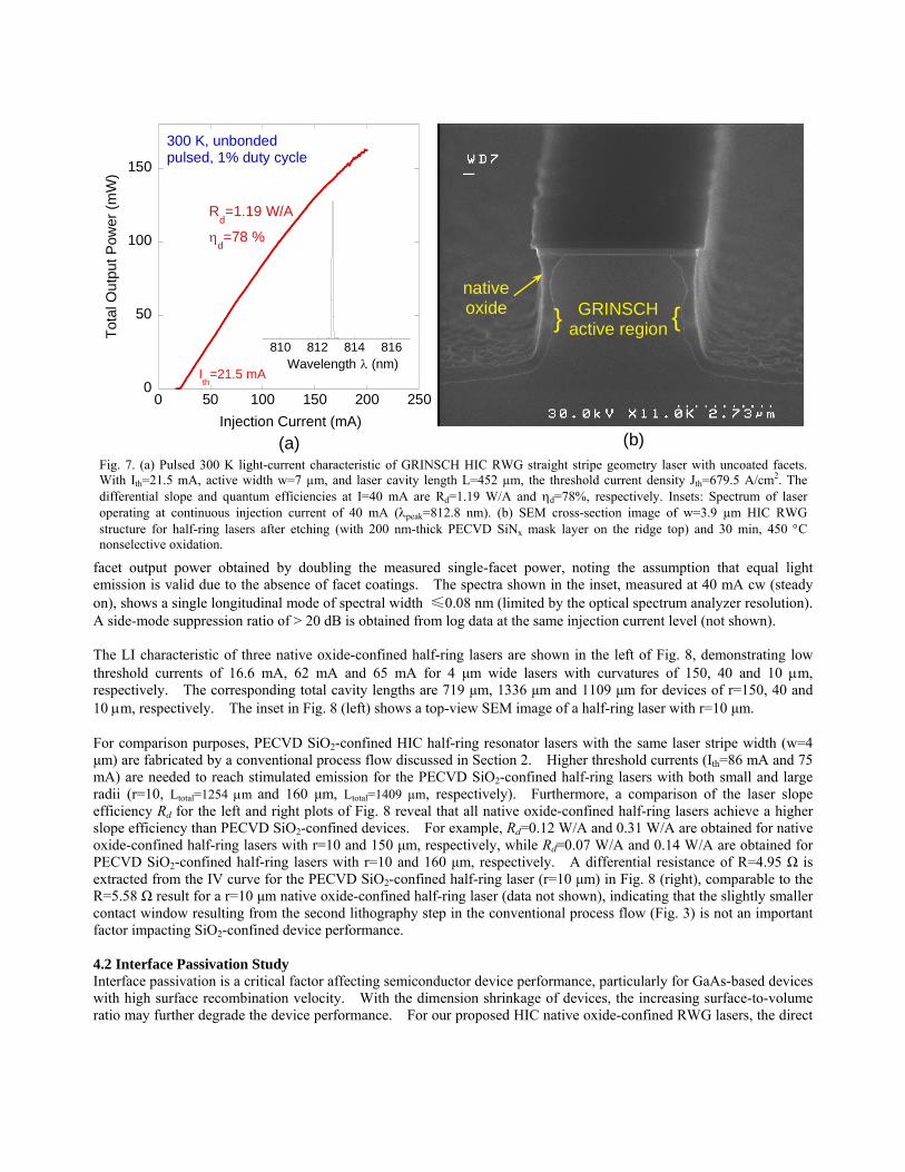
facet output power obtained by doubling the measured single-facet power, noting the assumption that equal light emission is valid due to the absence of facet coatings. The spectra shown in the inset, measured at 40 mA cw (steady on), shows a single longitudinal mode of spectral width ≤0.08 nm (limited by the optical spectrum analyzer resolution). A side-mode suppression ratio of > 20 dB is obtained from log data at the same injection current level (not shown).
0
50
100
150
0 50 100 150 200 250
Tota
l Out
put P
ower
(mW
)
Injection Current (mA)
native oxide GRINSCH
active region
Rd=1.19 W/A
ηd=78 %
300 K, unbondedpulsed, 1% duty cycle
Ith=21.5 mA
810 812 814 816Wavelength λ (nm)
(a) (b)
Fig. 7. (a) Pulsed 300 K light-current characteristic of GRINSCH HIC RWG straight stripe geometry laser with uncoated facets. With Ith=21.5 mA, active width w=7 µm, and laser cavity length L=452 µm, the threshold current density Jth=679.5 A/cm2. The differential slope and quantum efficiencies at I=40 mA are Rd=1.19 W/A and ηd=78%, respectively. Insets: Spectrum of laser operating at continuous injection current of 40 mA (λpeak=812.8 nm). (b) SEM cross-section image of w=3.9 µm HIC RWG structure for half-ring lasers after etching (with 200 nm-thick PECVD SiNx mask layer on the ridge top) and 30 min, 450 °C nonselective oxidation.
The LI characteristic of three native oxide-confined half-ring lasers are shown in the left of Fig. 8, demonstrating low threshold currents of 16.6 mA, 62 mA and 65 mA for 4 μm wide lasers with curvatures of 150, 40 and 10 μm, respectively. The corresponding total cavity lengths are 719 μm, 1336 μm and 1109 μm for devices of r=150, 40 and 10 μm, respectively. The inset in Fig. 8 (left) shows a top-view SEM image of a half-ring laser with r=10 μm. For comparison purposes, PECVD SiO2-confined HIC half-ring resonator lasers with the same laser stripe width (w=4 μm) are fabricated by a conventional process flow discussed in Section 2. Higher threshold currents (Ith=86 mA and 75 mA) are needed to reach stimulated emission for the PECVD SiO2-confined half-ring lasers with both small and large radii (r=10, Ltotal=1254 μm and 160 μm, Ltotal=1409 µm, respectively). Furthermore, a comparison of the laser slope efficiency Rd for the left and right plots of Fig. 8 reveal that all native oxide-confined half-ring lasers achieve a higher slope efficiency than PECVD SiO2-confined devices. For example, Rd=0.12 W/A and 0.31 W/A are obtained for native oxide-confined half-ring lasers with r=10 and 150 μm, respectively, while Rd=0.07 W/A and 0.14 W/A are obtained for PECVD SiO2-confined half-ring lasers with r=10 and 160 μm, respectively. A differential resistance of R=4.95 Ω is extracted from the IV curve for the PECVD SiO2-confined half-ring laser (r=10 μm) in Fig. 8 (right), comparable to the R=5.58 Ω result for a r=10 μm native oxide-confined half-ring laser (data not shown), indicating that the slightly smaller contact window resulting from the second lithography step in the conventional process flow (Fig. 3) is not an important factor impacting SiO2-confined device performance. 4.2 Interface Passivation Study Interface passivation is a critical factor affecting semiconductor device performance, particularly for GaAs-based devices with high surface recombination velocity. With the dimension shrinkage of devices, the increasing surface-to-volume ratio may further degrade the device performance. For our proposed HIC native oxide-confined RWG lasers, the direct

contact of the native oxide formed in the non-selective oxidation with the active region could be quite problematic if the nonselective oxide does not form a high quality, low-defect interface with the semiconductor. Fig. 9 demonstrates that the laser performance of narrow stripe (w~7 μm) lasers passivated by the native oxide is much better than PECVD SiO2-passivated devices. A laser diode with a short cavity usually demonstrates a higher slope efficiency due to a higher distributed mirror loss, which is the part of energy escaping the resonance cavity and released as the output power. It also requires less current to reach population inversion (i.e., stimulated emission) than one with a longer cavity because of a smaller cavity volume. So, if the PECVD SiO2 provided better or comparable passivation relative to the native oxide, a PECVD SiO2-confined, 335 μm long laser should have a higher slope efficiency and a lower threshold current than a native oxide-confined laser with a cavity length of 590 μm. However, compared with a threshold current of 24 mA and a slope efficiency of 1.1 W/A achieved on a native-oxide confined laser under a pulsed operation (1% duty cycle), the PECVD SiO2-confined laser needs a higher current to reach threshold (Ith=40 mA) and exhibits a lower slope efficiency (Rd=0.65 W/A), indicating the widely used PECVD SiO2 is not nearly as good as the non-selective native oxide in passivating surface states. Without any heat sink, when both laser types are measured under a fast-cw condition (a fast dc current sweep time of ~ 0.34 sec), Fig. 9 shows that the native oxide-confined laser can still start lasing at low threshold current and follow the pulsed LI curve without rolling over until I~160 mA. In contrast, under fast-cw operation the PECVD SiO2-confined laser experiences a higher threshold and lower efficiency with a “rollover” of output (usually associated with heat) beginning at I~120 mA which suggests a poorer thermal performance of PECVD SiO2-confined devices. Surprisingly, the native oxide-confined laser tested p-side up without a heat sink shows a true cw (steady state) threshold of only Ith=26 mA, just 2 mA higher than the pulsed threshold current, with no LI curve roll over until I=125 mA. No data was taken above 125 mA to prevent possible thermal damage to the device. The oxidation smoothing discussed in Section 2 may also play a role with the GRINSCH structure used here, resulting in a lower scattering loss than that of PECVD SiO2-confined devices. The above comparisons between threshold currents and efficiencies of native-oxide and PECVD SiO2-confined devices are not fully accurate because these device performance parameters also depends on the laser cavity length which is inversely proportional to the distributed mirror loss. A study of surface quality at the interface of native oxide/semiconductor and PECVD SiO2/semiconductor is therefore conducted below by selecting two straight devices with almost identical cavity length. The passivation capability of the non-selective oxides is also explored by studying the threshold current density and efficiency of lasers on the same length bar with varying stripe width. Similar deep-etched lasers passivated by PECVD SiO2 with similar thickness (~150 nm) and refractive index (~1.7) to the native oxide
Fig. 8. Left: Pulsed (0.05% duty cycle, unbonded, uncoated facets, 300 K) LI characteristic of native oxide-confined half-ring resonator lasers with radii of 10 (Ltotal=1109 μm), 40 (Ltotal=1336 μm) and 150 µm (Ltotal=719 μm), respectively; Right: PECVD SiO2-confined half-ring resonator lasers (right) with radii of 10 (Ltotal=1254 μm) and 160 µm (Ltotal=1409 μm). IV curve of r=10 m PECVD-SiO2 half-ring laser is shown on the right. Inset (left): top-view SEM image of a half-ring laser with r=10 µm.

Fig. 9. Total output power as a function of injection current (pulsed, quasi-cw and true cw) for a native oxide-confined laser (w=7.7 μm, L=590 μm) and a PECVD SiO2-confined laser (w=7 μm, L=335 μm).
0
500
1000
1500
2000
2500
0
20
40
60
80
100
120
0 20 40 60 80 100
PECVD SiO2-confined
Native oxide-confined
Thre
shol
d C
urre
nt D
ensi
ty (A
/cm
2 )
Threshold Current (m
A)
Laser Stripe Width (μm)
L=335 μm
L=333.7 μm
Fig. 10. Threshold current and threshold current density as a function of the stripe width for a native oxide-confined laser (w=5 μm, L=333.7 μm) and a PECVD SiO2-confined laser (w=5 μm, L=335 μm). Lasers are measured under pulsed mode with a 1% duty cycle.
are also fabricated in a conventional process flow (Fig. 3) for comparison purpose. Results of this stripe width-dependent study are shown in Fig. 10 where the threshold current and corresponding current densities of native oxide-confined and PECVD SiO2-confined lasers with nearly identical structure dimensions are plotted as a function of the laser stripe width. As the laser stripe width decreases, the lasing threshold current densities increase rapidly but at different rates for both laser types. Native oxide-confined lasers clearly demonstrate a smaller increase, especially in the narrow stripe range (w<10 μm). For a native oxide-confined laser, the threshold current density at w=5 μm is only 978 A/cm2 (3.4×) higher than that of a laser with w=40 μm. For a w= 5 μm PECVD SiO2-confined device, the value of 1590 A/cm2 is 3.8× higher than at w=40 μm. At w<15 µm, the SiO2-insulated devices have approximately 2× higher threshold current densities than the native-oxide devices because the non-radiative recombination becomes the dominate electrical loss in narrow stripe devices. An overall lower threshold current density of native oxide-confined lasers further proves the superior interface passivation of the native oxide relative to the deposited dielectric.
5. CONCLUSION Motivated by the desirable enhancements in photonic integrated circuit (PIC) design flexibility and chip function density that a high-index-contrast (HIC) waveguide structure can provide, we have proposed and implemented a new deep-etch plus partial non-selective oxidation smoothing process to achieve a HIC ridge waveguide (RWG) structure with a simplified fabrication process which promises to significantly improve the device performance. Several desirable features including SWR smoothing, self-aligned processing and effective optical and carrier confinement have been found to result from the application of non-selective oxidation of AlGaAs heterostructures. A theoretical study of the relationship of index contrast and SWR to the waveguide propagation loss has been conducted. A smooth interface with a SWR reduced down to 1 nm (a roughness reduction of as much as 100 fold) has been demonstrated after non-selective oxidation. The O2 content has been shown to be the key parameter for effective oxidation smoothing. HIC AlGaAs/GaAs ridge geometry waveguides have been fabricated. Both HIC AlGaAs native oxide-confined and plasma-enhanced chemical vapor deposition (PECVD) SiO2-confined RWG lasers in straight and half-ring geometries have been successfully fabricated from a graded-index separate-confinement heterostructure (GRINSCH) diode laser wafer and characterized, with low threshold current, high efficiency HIC RWG laser operation observed. A sharply bent half-ring laser diode with a record low radius of curvature of 10 μm has been achieved, demonstrating that a low bend loss HIC structure with low scattering loss at the semiconductor/oxide interface has been realized.

Interface non-radiative recombination has been studied by comparing native oxide-confined and PECVD SiO2-confined straight lasers of varying stripe width. The lower threshold current density and higher efficiency of native-oxide-confined lasers proves that the high-quality non-selective thermal native oxide provides better surface state passivation than a deposited PECVD dielectric.
REFERENCES [1] K. K. Lee, D. R. Lim, L. G. Kimerling, J. Shin, and F. Cerrina, "Fabrication of ultralow-loss Si/SiO2
waveguides by roughness reduction," Opt. Lett., vol. 26, pp. 1888-1890, 2001. [2] J. M. Dallesasse, N. Holonyak, Jr., A. R. Sugg, T. A. Richard, and N. El-Zein, "Hydrolyzation oxidation of
AlxGa1-xAs-AlAs-GaAs quantum well heterostructures and superlattices," App. Phy. Lett., vol. 57, pp. 2844-2846, 1990.
[3] Y. Luo, D. C. Hall, R. M. Sieg, A. A. Allerman, O. Blum, and H. Q. Hou, "Non-Selective Wet Oxidation of AlGaAs Heterostructure Waveguides via Controlled Addition of Oxygen," IEEE J. Sel. Top. in Quantum Electron., vol. 11, Nov./Dec. 2005.
[4] M. Passlack, M. Hong, E. F. Schubert, J. R. Kwo, J. P. Mannaerts, S. N. G. Chu, N. Moriya, and F. A. Thiel, "In situ fabricated Ga2O3--GaAs structures with low interface recombination velocity," App. Phy. Lett., vol. 66, pp. 625-627, 1995.
[5] B. E. A. Saleh and M. C. Teich, Fundamentals of Photonics: John Wiley and Sons Inc, 1991. [6] V. Van, P. P. Absil, J. V. Hryniewicz, and P.-T. Ho, "Propagation loss in single-mode GaAs-AlGaAs microring
resonators: measurement and model," IEEE J. Lightwave Technol., vol. 19, pp. 1734-1739, 2001. [7] T. Suligoj, K. L. Wang, and P. Biljanovic, "Minimization of sidewall roughness in Si pillar-like structures by
photolithography optimization," presented at Electrotechnical Conference, 2002. MELECON 2002. 11th Mediterranean, 2002.
[8] D. Liang, "Silicon-On-Insulator (SOI) Single-Mode Rib Waveguides, Simulation, Fabrication and Characterization.," in Department of Electrical Engineering. Notre Dame: University of Notre Dame, 2004, pp. 87.
[9] S. W. Pang, W. D. Goodhue, T. M. Lyszczarz, D. J. Ehrlich, R. B. Goodman, and G. D. Johnson, "Dry etching induced damage on vertical sidewalls of GaAs channel," J. Vac. Sci. Technol. B, vol. 6, pp. 1916-1920, 1988.
[10] W. H. Juan and S. W. Pang, "Controlling sidewall smoothness for micromachined Si mirrors and lenses," presented at The 40th international conference on electron, ion, and photon beam technology and nanofabrication, Atlanta, Georgia (USA), 1996.
[11] Y. Luo, D. C. Hall, L. Kou, O. Bium, H. Hou, L. Steingart, and J. H. Jackson, "Optical properties of AlxGa1-xAs heterostructure native oxide planar waveguides," presented at Lasers and Electro-Optics Society 1999 12th Annual Meeting. LEOS '99. IEEE, 1999.
[12] D. C. Hall, H. Wu, L. Kou, Y. Luo, R. J. Epstein, O. Blum, and H. Hou, "Refractive index and hygroscopic stability of AlxGa1-xAs native oxides," App. Phy. Lett., vol. 75, pp. 1110-1112, 1999.
[13] A. G. Rickman, G. T. Reed, and F. Namavar, "Silicon-on-insulator optical rib waveguide loss and mode characteristics," IEEE J. Lightwave Technol., vol. 12, pp. 1771-1776, 1994.
[14] P. K. Tien, "Light waves in thin films and integrated optics," App. Opt., vol. 10, pp. 2395-2413, 1971. [15] M. V. Bazylenko, M. Gross, and M. Faith, "Effect of reactive ion etching--generated sidewall roughness on
propagation loss of buried-channel silica waveguides," App. Phy. Lett., vol. 69, pp. 2178-2180, 1996. [16] R. J. Deri and E. Kapon, "Low-loss III-V semiconductor optical waveguides," IEEE J. Quantum Electron., vol.
27, pp. 626-640, 1991. [17] S. Suzuki, M. Yanagisawa, Y. Hibino, and K. Oda, "High-density integrated planar lightwave circuits using
SiO2-GeO2 waveguides with a high refractive index difference," IEEE J. Lightwave Technol., vol. 12, pp. 790-796, 1994.
[18] K. K. Lee, D. R. Lim, H.-C. Luan, A. Agarwal, J. Foresi, and L. C. Kimerling, "Effect of size and roughness on light transmission in a Si/SiO2 waveguide: Experiments and model," App. Phy. Lett., vol. 77, pp. 1617-1619, 2000.
[19] M. K. Chin, C. Youtsey, W. Zhao, T. Pierson, Z. Ren, S. L. Wu, L. Wang, Y. G. Zhao, and S. T. Ho, "GaAs microcavity channel-dropping filter based on a race-track resonator," IEEE J. Lightwave Technol., IEEE, vol. 11, pp. 1620-1622, 1999.
[20] D. Rafizadeh, J. P. Zhang, R. C. Tiberio, and S. T. Ho, "Propagation loss measurements in semiconductor microcavity ring and disk resonators," IEEE J. Lightwave Technol., vol. 16, pp. 1308-1314, 1998.
[21] J. W. Bae, W. Zhao, J. H. Jang, I. Adesida, A. Lepore, M. Kwakernaak, and J. H. Abeles, "Characterization of sidewall roughness of InP/InGaAsP etched using inductively coupled plasma for low loss optical waveguide applications," J. Vac. Sci. Technol. B, vol. 21, pp. 2888-2891, 2003.
[22] J. S. Roberts, J. P. R. David, L. Smith, and P. L. Tihanyi, "The Influence of Trimethylindium Impurities on The Performance of InAlGaAs Single Quantum Well Lasers," J. Crystal Growth, vol. 195, pp. 668-675, 1998.