high-frequency analysis of circuitste.kmutnb.ac.th/~msn/224510highfrequency.pdf · analysis of...
TRANSCRIPT
1
Asst. Prof. Dr. MONTREE SIRIPRUCHYANUN
1
High-Frequency Analysis of Circuits
Asst. Prof. MONTREE SIRIPRUCHYANUN, D. Eng.Dept. of Teacher Training in Electrical Engineering,
Faculty of Technical EducationKing Mongkut’s Institute of Technology North Bangkok
http://www.te.kmitnb.ac.th/[email protected]
224510 Advanced coomunication circuit design 2
Overview
• Background– So far, our treatment of small-signal analysis of amplifiers has been
for low frequencies where internal capacitances do not affect operation. However, we will see that internal capacitances do exist. We will see how these capacitances affect the frequency responseof amplifiers and why we modeled real op amps to have a frequency response with a single dominant pole.To fully understand and model the frequency response of amplifiers, we utilize Bode plots again. We will look at two methods to facilitate the high-frequency circuit analysis. One technique called open-circuit time constant (OCT) method approximates the high-frequency response by calculating the time constant associated with each capacitor in a circuit. Miller’s theorem provides a way to deal with bridging capacitors (between input and output).
– In this lecture, we will focus on understanding and analyzing the frequency response of MOSFET-based amplifiers. High-frequency analysis of BJT-based amplifiers are similar.
2
Asst. Prof. Dr. MONTREE SIRIPRUCHYANUN
224510 Advanced coomunication circuit design 3
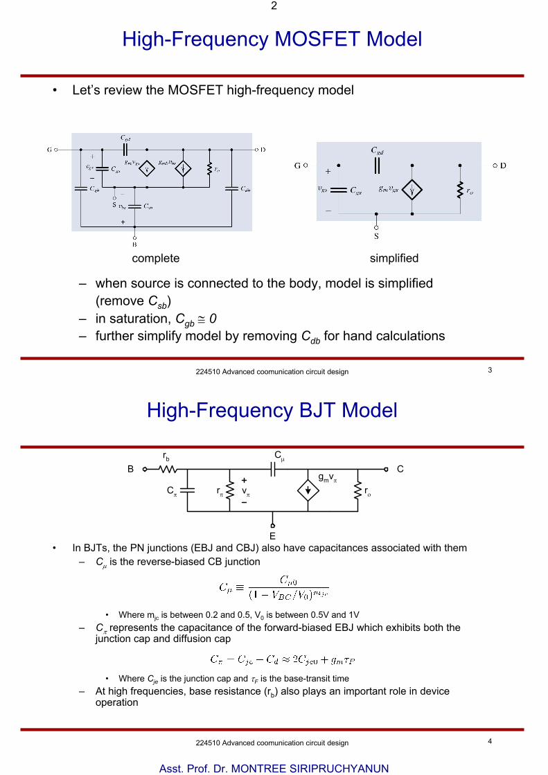
High-Frequency MOSFET Model
• Let’s review the MOSFET high-frequency model
– when source is connected to the body, model is simplified (remove Csb)
– in saturation, Cgb ≅ 0– further simplify model by removing Cdb for hand calculations
complete simplified
224510 Advanced coomunication circuit design 4
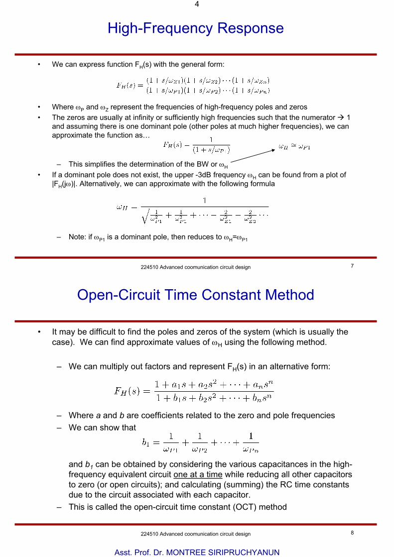
High-Frequency BJT Model
• In BJTs, the PN junctions (EBJ and CBJ) also have capacitances associated with them – Cμ is the reverse-biased CB junction
• Where mjc is between 0.2 and 0.5, V0 is between 0.5V and 1V– Cπ represents the capacitance of the forward-biased EBJ which exhibits both the
junction cap and diffusion cap
• Where Cje is the junction cap and τF is the base-transit time– At high frequencies, base resistance (rb) also plays an important role in device
operation
Cμ
Cπ rπ
gmvπ
rο
rb
B
E
C
vπ

3
Asst. Prof. Dr. MONTREE SIRIPRUCHYANUN
224510 Advanced coomunication circuit design 5
Amplifier Transfer Function
• Voltage-gain frequency response of amplifiers seen so far take one of two forms– Direct-Coupled (DC) amplifiers exhibit low-pass characteristics
flat gain from DC to ωH– Capacitively-coupled amplifiers exhibit band-pass characteristics – attenuation at low
frequency due to impedance from coupling capacitances increasing for low frequencies• We will focus on the high-frequency portion of the response (ωH)
– Gain drops due to effects of internal capacitances of the device• Bandwidth is the frequency range over which gain is flat
– BW = ωH or ωH-ωL ≈ ωH (ωH >> ωL)• Gain-Bandwidth Product (GB) – Amplifier figure of merit
– GB ≡ AMωHwhere AM is the midband gain
– We will see later that it is possible to trade off gain for bandwidth
-3dB
ωH ω
A0
|A| (dB)
-3dB
ωH ω
AM
|A| (dB)
ωL
224510 Advanced coomunication circuit design 6
Gain Function A(s)
• We can represent the frequency dependence of gain with the following expression:
– Where FL(s) and FH(s) are the functions that account for the frequency dependence of gain on frequency at the lower and upper frequency ranges
• We will use open-circuit time constant method to find FH(s)• Assume FL(s) = 1 for now
– We can solve for AM by assuming that large coupling capacitors are short circuits and internal device capacitances are open circuits (what we have done so far for low-frequency small-signal analysis)
4
Asst. Prof. Dr. MONTREE SIRIPRUCHYANUN
224510 Advanced coomunication circuit design 7
High-Frequency Response
• We can express function FH(s) with the general form:
• Where ωP and ωZ represent the frequencies of high-frequency poles and zeros• The zeros are usually at infinity or sufficiently high frequencies such that the numerator 1
and assuming there is one dominant pole (other poles at much higher frequencies), we can approximate the function as…
– This simplifies the determination of the BW or ωH
• If a dominant pole does not exist, the upper -3dB frequency ωH can be found from a plot of |FH(jω)|. Alternatively, we can approximate with the following formula
– Note: if ωP1 is a dominant pole, then reduces to ωH=ωP1
224510 Advanced coomunication circuit design 8
Open-Circuit Time Constant Method
• It may be difficult to find the poles and zeros of the system (which is usually the case). We can find approximate values of ωH using the following method.
– We can multiply out factors and represent FH(s) in an alternative form:
– Where a and b are coefficients related to the zero and pole frequencies– We can show that
and b1 can be obtained by considering the various capacitances in the high-frequency equivalent circuit one at a time while reducing all other capacitors to zero (or open circuits); and calculating (summing) the RC time constants due to the circuit associated with each capacitor.
– This is called the open-circuit time constant (OCT) method
5
Asst. Prof. Dr. MONTREE SIRIPRUCHYANUN
224510 Advanced coomunication circuit design 9
Calculating OCTs
The approach:• For each capacitor:
– set input signal to zero– replace all other capacitors with open circuits– find the effective resistance (Rio) seen by the capacitor Ci
• Sum the individual time constants (RCs or also called the open-circuit time constants)
• This method for determining b1 is exact. The approximation comes from using this result to determine ωH.
– This equation yields good results even if there is no single dominant pole but when all poles are real
• We will see an example of this method when we analyze the high-frequency response of different amplifier topologies
224510 Advanced coomunication circuit design 10
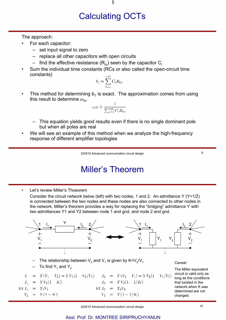
Miller’s Theorem
• Let’s review Miller’s ThoeoremConsider the circuit network below (left) with two nodes, 1 and 2. An admittance Y (Y=1/Z) is connected between the two nodes and these nodes are also connected to other nodes in the network. Miller’s theorem provides a way for replacing the “bridging” admittance Y with two admittances Y1 and Y2 between node 1 and gnd, and node 2 and gnd.
– The relationship between V2 and V1 is given by K=V2/V1
– To find Y1 and Y2
Y
V1 V2 Y1V1 V2Y2
I1 I2 I1 I21 21 2
Caveat:
The Miller equivalent circuit is valid only as long as the conditions that existed in the network when K was determined are not changed.

6
Asst. Prof. Dr. MONTREE SIRIPRUCHYANUN
224510 Advanced coomunication circuit design 11
High-Frequency Response of CS Amp
• Let’s now find the high-frequency response of a common-source amplifier– First, redraw using a high-frequency small-signal model for the nMOS
• There are three ways to find the upper 3-dB frequency ωH
– Use open-circuit time constant method– Use Miller’s theorem– Brute force calculations to find vout/vin
• Let’s investigate them all
224510 Advanced coomunication circuit design 12
Using OCT on CS Amplifier
• Find the RC time constants associated with Cgd and Cgs in the following circuit
• Replace Cgd with an open circuit and find the resistance seen by Cgs
• Replace Cgs with an open-ckt and find the resistance seen by Cgd
Rs
Cgd
Cgs
gmvgs
vgs RL||ro vovi
Rs
gmvgs
RL||ro voItstvtst
Rs
gmvgs
RL||ro vo
itst
vtst
vgs

7
Asst. Prof. Dr. MONTREE SIRIPRUCHYANUN
224510 Advanced coomunication circuit design 13
Using OCTs Cont’d
• Summing the two time constants yields ωH
– From the above equation, it is not difficult to imagine that Cgd has a more significant effect on reducing BW
– The resulting frequency dependence of gain is…
• Let’s compare this result with what we get using Miller’s theorem
224510 Advanced coomunication circuit design 14
Using Miller’s Theorem on CS Amplifier
• Redraw the high-frequency small-signal model using Miller’s theorem
– Assuming a dominant pole introduced by Cgd in parallel with Cgs
– Miller multiplication of Cgd results in a large input capacitance• Notice that this approximation for ωH is close to the approximation found using OCT
assuming that RsCgd(1+gmRL’) dominates
• Let’s verify these two approaches by deriving the exact high-frequency transfer function of the CS amplifier
Rs
Cgd(1+gmRL')
Cgs
gmvgs
vgs RL' vovi
Cgd[1+1/(gmRL')]~= Cgd
CT

8
Asst. Prof. Dr. MONTREE SIRIPRUCHYANUN
224510 Advanced coomunication circuit design 15
High-Frequency Response of CS Amplifier
• Replace the input source and series resistance with a Norton equivalent
– The exact solution gives a zero (at a high frequency) and two poles– Notice that the s term (in the denominator) is the same as the solution using
the OCT method• Unfortunately, the denominator is too complicated to extract useful info as is.
So, assuming the two poles are widely separated (greater than an order of magnitude), we can rewrite the expression for the denominator as…
Notice zero is negative. This has implications on stability (we will see later)
Rs
Cgd
Cgs
gmvgs
vgs RL' vo
vi/Rs
sCgd(vgs-vo)
224510 Advanced coomunication circuit design 16
HF Response of CS Amplifier
• Rewrite the denominator as:
– And from the solution on the previous slide we can write…
• So the second pole is usually at a much higher frequency and we can assume a dominant pole (ωP1)
• Using either Miller’s theorem or OCTs enables a way to quickly find approximations of the amplifier’s high-frequency response
9
Asst. Prof. Dr. MONTREE SIRIPRUCHYANUN
224510 Advanced coomunication circuit design 17
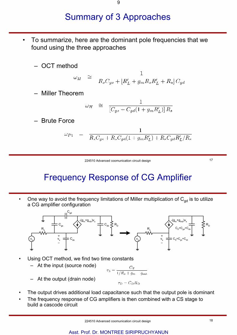
Summary of 3 Approaches
• To summarize, here are the dominant pole frequencies that we found using the three approaches
– OCT method
– Miller Theorem
– Brute Force
224510 Advanced coomunication circuit design 18
Frequency Response of CG Amplifier
• One way to avoid the frequency limitations of Miller multiplication of Cgd is to utilize a CG amplifier configuration
• Using OCT method, we find two time constants– At the input (source node)
– At the output (drain node)
• The output drives additional load capacitance such that the output pole is dominant• The frequency response of CG amplifiers is then combined with a CS stage to
build a cascode circuit
vx
RD
vs
Rs
Cgs
Cgd
Csb
Cdb
-(gm+gmb)vx
vx
RD
vs
Rs
CS=Cgs+Csb
CD=Cgd+Cdb
-(gm+gmb)vx
10
Asst. Prof. Dr. MONTREE SIRIPRUCHYANUN
224510 Advanced coomunication circuit design 19
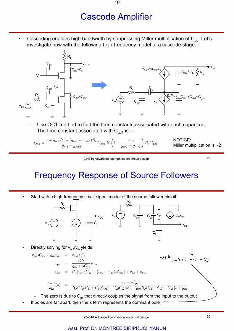
Cascode Amplifier
• Cascoding enables high bandwidth by suppressing Miller multiplication of Cgd. Let’s investigate how with the following high-frequency model of a cascode stage.
– Use OCT method to find the time constants associated with each capacitor. The time constant associated with Cgd1 is…
Vb
vIN
vOUT
Cgd1
Cgs1
Cdb1+Csb2
Cdb2+CL
RL
Cgd2
Cgs2
Rs
Cgs1
RL
vin
Rs Cgd1
gmvgs1 Cdb1+Csb2+Cgs2
Cdb2+CL-gm2+gmb2vx
vx
vout
NOTICE:Miller multiplication is ~2
224510 Advanced coomunication circuit design 20
Frequency Response of Source Followers
• Start with a high-frequency small-signal model of the source follower circuit
• Directly solving for vout/vin yields:
– The zero is due to Cgs that directly couples the signal from the input to the output• If poles are far apart, then the s term represents the dominant pole
Rs
CL
vOUT
vIN
Rs
vin
vout
CL
Cgsgmvgs
vgsCgd
11
Asst. Prof. Dr. MONTREE SIRIPRUCHYANUN
224510 Advanced coomunication circuit design 21
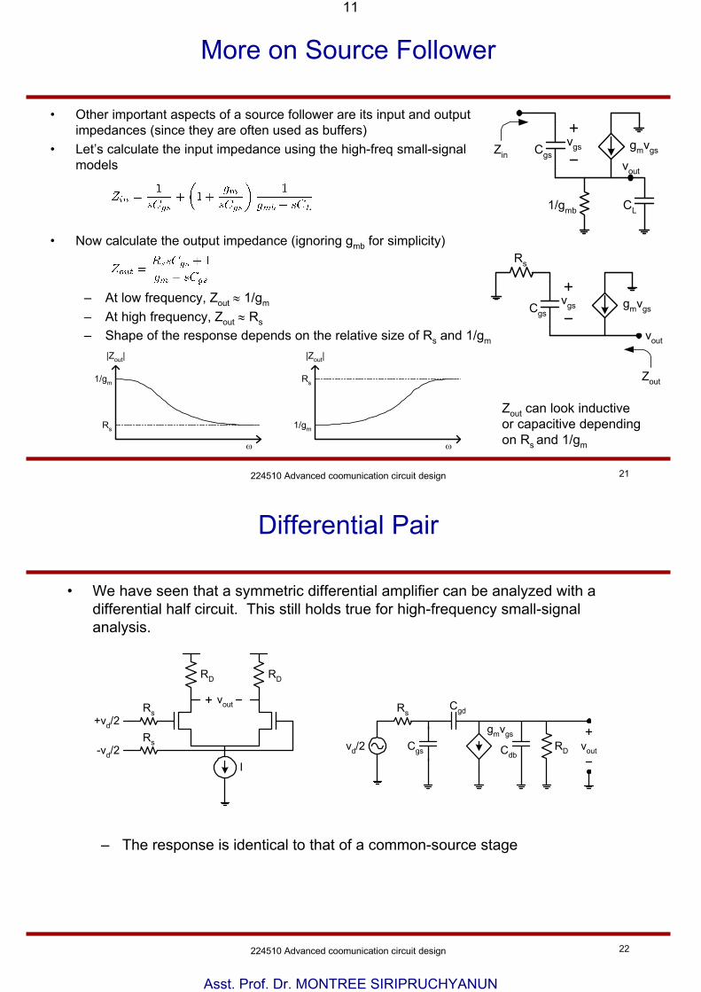
More on Source Follower
• Other important aspects of a source follower are its input and output impedances (since they are often used as buffers)
• Let’s calculate the input impedance using the high-freq small-signal models
• Now calculate the output impedance (ignoring gmb for simplicity)
– At low frequency, Zout ≈ 1/gm
– At high frequency, Zout ≈ Rs
– Shape of the response depends on the relative size of Rs and 1/gm
vout
CL
Cgsgmvgs
vgsZin
1/gmb
vout
Cgsgmvgs
vgs
Zout
Rs
1/gm
Rs 1/gm
Rs
|Zout||Zout|
ω ω
Zout can look inductive or capacitive depending on Rs and 1/gm
224510 Advanced coomunication circuit design 22
Differential Pair
• We have seen that a symmetric differential amplifier can be analyzed with a differential half circuit. This still holds true for high-frequency small-signal analysis.
– The response is identical to that of a common-source stage
RD RD
I
vout
+vd/2
-vd/2
Rs
Rs
Rs
Cgs
gmvgs
Cdb
Cgd
voutvd/2 RD

12
Asst. Prof. Dr. MONTREE SIRIPRUCHYANUN
224510 Advanced coomunication circuit design 23
High-Frequency CMRR
• The CMRR of a differential pair degrades at high frequency due to a number of factors. The most important is the increase in CM gain with frequency due to capacitance on the tail node.
• Use the common-mode equivalent half circuit to understand how CM gain increases with frequency
– Draw the small-signal equivalent model and see the effect of CTAILon the vout/vin transfer function
– Zero at ωZ = 1/roCTAIL (since ro is big, ωZ occurs at a low frequency)– There are additional poles at higher frequencies due to CTAIL and
other internal capacitances (that we have ignored)• The zero causes the CM gain to increase with frequency until the higher
frequency poles kick in CMRR degrades due to the zero
RD
vout,CM
vin,CM
2ro CTAILI/2
vin,CM
vgs
2ro CTAIL
RD
gmvgsvout,CM
224510 Advanced coomunication circuit design 24
HF CMRR plots
• The impact of the zero in the CM gain on CMRR can be illustrated as shown
– Remember CMRR = Ad/Acm
• There is a trade off between CMRR and voltage headroom
– Wider current source devices enable lower vds
– Wider current source device means larger CTAIL
ω (log scale)ωZ
ωZ
ωP
ωP
ω (log scale)
ω (log scale)
CMRR (dB)
|Ad| (dB)
|Acm| (dB)
-20dB/dec
-40dB/dec

13
Asst. Prof. Dr. MONTREE SIRIPRUCHYANUN
224510 Advanced coomunication circuit design 25
Example: Diff Pair with Active Load
+vd/2
-vd/2
Q1 Q2
Q3 Q4
Q5
Cload
Vo
x
y• diff half circuit node x is virtual gnd
• Cy = Cgd1 + Cdb1 + Cgs3 + Cdb3 + Cgs4 + Cpar
• Cz = Cgd2 + Cdb2 + Cgd4 + Cdb4 + Cload
• Ro = ro4 // ro2
z
Vy =1
(gm3 + sCy)gm1 Vid
2
A =1
(1 + sCzRo)gm1 Ro (1 + sCz/gm)(1 + sCz/2gm)
Io = + gm3vy
gm2 Vid
2 Vo = RoIo
224510 Advanced coomunication circuit design 26
Example: 2 Stage CMOS Op Amp
+vd/2
-vd/2
Q1 Q2
Q3 Q4
Q5
Q6
Q7
Cc
Cload
Gm1 R1 C1 Gm2 R2 C2
Cx
• Gm1=gm1 =gm2
• Gm2=gm6
• R1= ro2 // ro4
• R2= ro6 // ro7
• R1= ro2 // ro4
• C1= Cgd2 + Cdb2+ Cgd4 + Cdb4+ Cgs6
• C2= Cgd7 + Cdb7 + Cdb6+ Cload
• Cx= Cc + Cgd6A = Gm1R1 Gm2R2
Using OCT:
dominant pole is at (Gm2R2)CxR1
unity gain freq is at Gm1/Cx
next pole is at C2/Gm2How do you determine the phase margin?