high-efficiency algainp light-emitting diodes for solid-state lighting applications
TRANSCRIPT

High-efficiency AlGaInP light-emitting diodes for solid-state lighting applicationsTh. Gessmann and E. F. Schubert Citation: Journal of Applied Physics 95, 2203 (2004); doi: 10.1063/1.1643786 View online: http://dx.doi.org/10.1063/1.1643786 View Table of Contents: http://scitation.aip.org/content/aip/journal/jap/95/5?ver=pdfcov Published by the AIP Publishing Articles you may be interested in Enhancement of light-extraction efficiency in AlGaInP light-emitting diodes using evanescent wave couplingeffect Appl. Phys. Lett. 103, 231112 (2013); 10.1063/1.4842215 Metal mirror assisting light extraction from patterned AlGaInP light-emitting diodes Appl. Phys. Lett. 94, 101102 (2009); 10.1063/1.3097017 Progress in AlInN–GaN Bragg reflectors: Application to a microcavity light emitting diode J. Appl. Phys. 97, 084505 (2005); 10.1063/1.1872197 Effect of current spreading on luminescence improvement in selectively oxidized AlGaInP light-emitting diodes J. Vac. Sci. Technol. B 21, 1157 (2003); 10.1116/1.1577572 Experimental determination of the internal quantum efficiency of AlGaInP microcavity light-emitting diodes J. Appl. Phys. 91, 2563 (2002); 10.1063/1.1433938
[This article is copyrighted as indicated in the article. Reuse of AIP content is subject to the terms at: http://scitation.aip.org/termsconditions. Downloaded to ] IP:
131.193.242.161 On: Tue, 09 Dec 2014 17:47:10
APPLIED PHYSICS REVIEWS—FOCUSED REVIEW
High-efficiency AlGaInP light-emitting diodes for solid-statelighting applications
Th. Gessmanna) and E. F. SchubertDepartment of Electrical, Computer, and Systems Engineering, Rensselaer Polytechnic Institute,Troy, New York 12180
~Received 11 July 2003; accepted 1 December 2003!
AlGaInP lattice matched to GaAs is suited for light-emitting diodes~LEDs! operating in the red,orange, yellow, and yellow–green wavelength range. Such long-wavelength visible-spectrumdevices will play an important role in solid-state lighting applications. This review discusses themajor classes of AlGaInP device structures, including absorbing-substrate~AS! LEDs, absorbingsubstrate LEDs enhanced by distributed-Bragg-reflectors~DBRs!, transparent substrate~TS! LEDs,thin-film ~TF! LEDs, and LEDs using omnidirectional reflectors~ODRs!. Some of these devicestructures have well-known deficiencies: A significant fraction of light is absorbed in the GaAssubstrate in AS-LEDs; DBRs are essentially transparent at oblique angles of incidence leading tosubstantial optical losses. More recent developments such as TS-LEDs and TF-LEDs avoid thesedrawbacks. High-reflectivity, electrically conductive ODRs were recently developed thatconsiderably outperform conventional distributed Bragg reflectors. LEDs using such conductiveODRs can replace DBRs in AlGaInP LEDs and are potential candidates for low-cost high-efficiencyLEDs suitable for high-power solid-state lighting applications. ©2004 American Institute ofPhysics. @DOI: 10.1063/1.1643786#
TABLE OF CONTENTS
I. INTRODUCTION. . . . . . . . . . . . . . . . . . . . . . . . . . . .2203II. AlGaInP LEDs IN SOLID-STATE LIGHTING
APPLICATIONS. . . . . . . . . . . . . . . . . . . . . . . . . . . .2204III. EARLY DEVELOPMENT OF THE AlGaInP
MATERIAL SYSTEM. . . . . . . . . . . . . . . . . . . . . . .2204IV. ABSORBING-SUBSTRATE LEDs~AS LEDs!... 2205V. DISTRIBUTED-BRAGG-REFLECTOR-
ENHANCED ABSORBING SUBSTRATE LEDs~DBR-LEDs!. . . . . . . . . . . . . . . . . . . . . . . . . . . . . . .2205
VI. HIGH EXTRACTION STRATEGIES FORAlGaInP LEDs. . . . . . . . . . . . . . . . . . . . . . . . . . . . .2206
A. Transparent-substrate LEDs. . . . . . . . . . . . . . . . . 2206B. Surface-textured LEDs. . . . . . . . . . . . . . . . . . . . .2207C. Photonic-crystal LEDs. . . . . . . . . . . . . . . . . . . . .2208D. Thin-film LEDs. . . . . . . . . . . . . . . . . . . . . . . . . .2208
VII. CONCEPTS FOR REFLECTINGSTRUCTURES. . . . . . . . . . . . . . . . . . . . . . . . . . . .2209
VIII. OMNIDIRECTIONAL REFLECTOR ~ODR!FOR LEDs. . . . . . . . . . . . . . . . . . . . . . . . . . . . . . .2210
IX. CHARACTERISTICS OF ODR-LEDs. . . . . . . . . . 2211X. WAFER BONDING FOR AlGaInP ODR-LEDs... 2214XI. CONCLUSIONS. . . . . . . . . . . . . . . . . . . . . . . . . . .2215
I. INTRODUCTION
Early materials used for light-emitting diodes~LEDs!emitting in the long-wavelength part of the visible spectrumwere GaP doped with isoelectronic impurities such as nitro-gen and GaAsP~for a review, see Schubert!.1 These materialssuffer from low efficiency and output power: GaAsP is lat-tice mismatched to GaAs and therefore has many disloca-tions; GaP:N lacks high-power capabilities due to the satu-ration of radiative recombination at high injection-currentlevels. AlGaAs is a high-efficiency material suitable for in-frared and red wavelengths~for a review, see Steranka!.2
However it is unsuitable for orange and shorter wavelengthsdue to the direct-indirect transition of the AlxGa12xAs bandgap atx'45% corresponding to a wavelength of 624 nm.
AlGaInP is the material of choice for the long-wavelength part of the visible spectrum, namely for red, or-ange, yellow, and yellow–green wavelengths. At the molarIn composition of 50%, (AlxGa12x)0.5In0.5P is latticematched to GaAs. Unlike GaAsP, which is also grown onGaAs, AlGaInP does not suffer from lattice mismatch. Un-like GaP:N, AlGaInP does not rely on deep-level-mediatedtransitions that tend to saturate. Similar to AlGaAs, AlGaInPsuffers from a direct-indirect transition of the band gap.However, the direct-indirect transition in AlGaInP occurs at ahigher energy compared with AlGaAs. As a result, theAlGaInP materials system can be used for all colors of thelong-wavelength region of the visible spectrum down toyellow–green wavelengths.
a!Author to whom correspondence should be addressed; electronic mail:[email protected]
JOURNAL OF APPLIED PHYSICS VOLUME 95, NUMBER 5 1 MARCH 2004
22030021-8979/2004/95(5)/2203/14/$22.00 © 2004 American Institute of Physics
[This article is copyrighted as indicated in the article. Reuse of AIP content is subject to the terms at: http://scitation.aip.org/termsconditions. Downloaded to ] IP:
131.193.242.161 On: Tue, 09 Dec 2014 17:47:10

The AlGaInP band gap energy, the corresponding wave-lengths, and the nature of the band gap~direct or indirect!,are shown in Fig. 1. The vertical dashed line in the figureindicates the composition at which AlGaInP is lattice-matched to GaAs. The direct-indirect transition of the band-gap occurs at the energy of 2.23–2.33 eV corresponding to556–532 nm. The exact energy at which the direct–indirecttransition occurs depends on the degree of randomness of thequaternary alloy semiconductor and is lower for AlGaInPwith a high degree of order.3
The importance of AlGaInP LEDs as an instrumentalingredient in future solid-state lighting systems will be re-viewed. We will discuss the major technologies suitable forhigh-efficiency and high-power AlGaInP LEDs. Special em-phasis will be placed on the discussion of the limitations ofcurrent AlGaInP technologies and on emerging technologiessuch as AlGaInP LED structures employing omnidirectionalreflectors~ODRs! and thin-film ~TF! technologies using py-ramidal reflectors for enhanced light extraction.
II. AlGaInP LEDs IN SOLID-STATE LIGHTINGAPPLICATIONS
It is well known that semiconductor-based light sourceshave, in principle, the potential to achieving near-unitypower efficiency. This is in contrast to common conventionallight sources such as incandescent and fluorescent lamps thathave fundamental efficiency limitations that prevent themfrom reaching near-unity efficiencies. As low-cost sourcesthat provide high-efficiency and high power output are de-veloped, semiconductor light sources will replace fluorescentand inefficient incandescent sources.
Different semiconductor-based schemes to generatewhite light for general daylight illumination applications areshown in Fig. 2. The figure shows different approaches for~a! dichromatic, ~b! trichromatic, and ~c! tetrachromaticwhite light sources including single-chip semiconductorsources and multichip semiconductor sources. The figurealso shows semiconductor/phosphor-based sources includinga blue LED/yellow phosphor source, a blue and red LED/green phosphor source, and an ultraviolet~UV! LED/phosphor source. Tetrachromatic approaches offer outstand-
ing color rendering properties if the wavelength of eachsource and their temperature dependencies can be controlledaccurately. As a result, there is little motivation to developpentachromatic approaches, although such pentachromaticapproaches may be suitable for certain niche markets.
Several characteristics of the solid-state white sourcesshown in Fig. 2 are noteworthy. First, dichromatic ap-proaches have the highest luminous efficacy and they arewell suited for display and indicator-light applications. Dueto their low color rendering capabilities, their usefulness indaylight illumination and display backlighting applications islimited. Second, trichromatic approaches based on eitherLEDs or phosphors provide excellent color rendition with aCommission Internationale de l’ E´ clarge~CIE! general color-rendering index of 90 or higher.5 Third, due to the unavoid-able Stokes shift in the trichromatic UV-LED/phosphorsource, the potential luminous efficiency of this source islower compared with a trichromatic multichip LED ap-proach. Fourth, the trichromatic approach shown in Fig. 2consisting of a blue LED, a green phosphor, and a red LEDis motivated by the unavailability of highly efficient greensemiconductor-based emitters. The use of the red LED ismotivated by the availability of efficient red AlGaInP LEDs.In addition, the employment of red LEDs allows for theavoidance of the very large Stokes shift concomitant with theUV or blue LED/red phosphor combination. Therefore, thetwo LED/green phosphor approach promises both, good ef-ficiency and color rendering capabilities.
A detailed analysis5 and the preceding discussion of dif-ferent solid-state-lighting strategies make clear that the emis-sion sources with the highest luminous efficiencies and ex-cellent color rendering properties~>90! include red LEDs.With luminous efficiency and the resulting energy savings asstrong driving forces for solid-state lighting, large-scale useof AlGaInP LEDs is expected in future lighting systems.
III. EARLY DEVELOPMENT OF THE AlGaInPMATERIAL SYSTEM
The AlGaInP material system was developed in Japanfor visible lasers.6–9 Efforts started with AlGaInP/GaInPdouble-heterostructure lasers using Ga0.5In0.5P as the light-emitting active material, which is lattice matched to GaAs
FIG. 1. Band gap energy and corresponding wavelength vs lattice constantof (Al xGa12x)yIn12yP at 300 K. The dashed vertical line shows(Al xGa12x)0.5In0.5P lattice matched to GaAs~adopted from Ref. 4!.
FIG. 2. LED-based approaches for white light sources and correspondingoptical spectra. The highest luminous efficacy is provided by the dichro-matic approaches. The best color rendering is obtained with tetrachromaticapproaches. Trichromatic approaches based on LEDs can provide goodcolor rendering as well as high luminous efficacy.
2204 J. Appl. Phys., Vol. 95, No. 5, 1 March 2004 T. Gessmann and E. F. Schubert
[This article is copyrighted as indicated in the article. Reuse of AIP content is subject to the terms at: http://scitation.aip.org/termsconditions. Downloaded to ] IP:
131.193.242.161 On: Tue, 09 Dec 2014 17:47:10
substrates. The bandgap energy of lattice-matched~randomalloy! GaInP is approximately 1.9 eV~650 nm!, making thematerial suitable for visible lasers emitting in the red. Theselasers are used, for example, in digital versatile disc technol-ogy and in laser pointers. The addition of Al to GaInPallows one to attain shorter emission wavelengths includingthe orange and yellow spectral region. However,(Al xGa12x)0.5In0.5P becomes an indirect semiconductor at Alcompositions ofx'0.53, so that the radiative efficiencystrongly decreases at wavelengths near and, in particular, be-low 600 nm. Consequently, AlGaInP is not suited for high-efficiency emission at wavelengths below 570 nm. Reviewsof different aspects of the AlGaInP material system and Al-GaInP LEDs can be found in the literature.1,10–12
IV. ABSORBING-SUBSTRATE LEDs „AS LEDs …
Subsequent to the AlGaInP laser development that oc-curred in the early 1980s, AlGaInP LED development startedat the end of the 1980s and early 1990s.13–16 These LEDswere grown in ap-side-up configuration on conductiven-type GaAs substrates.
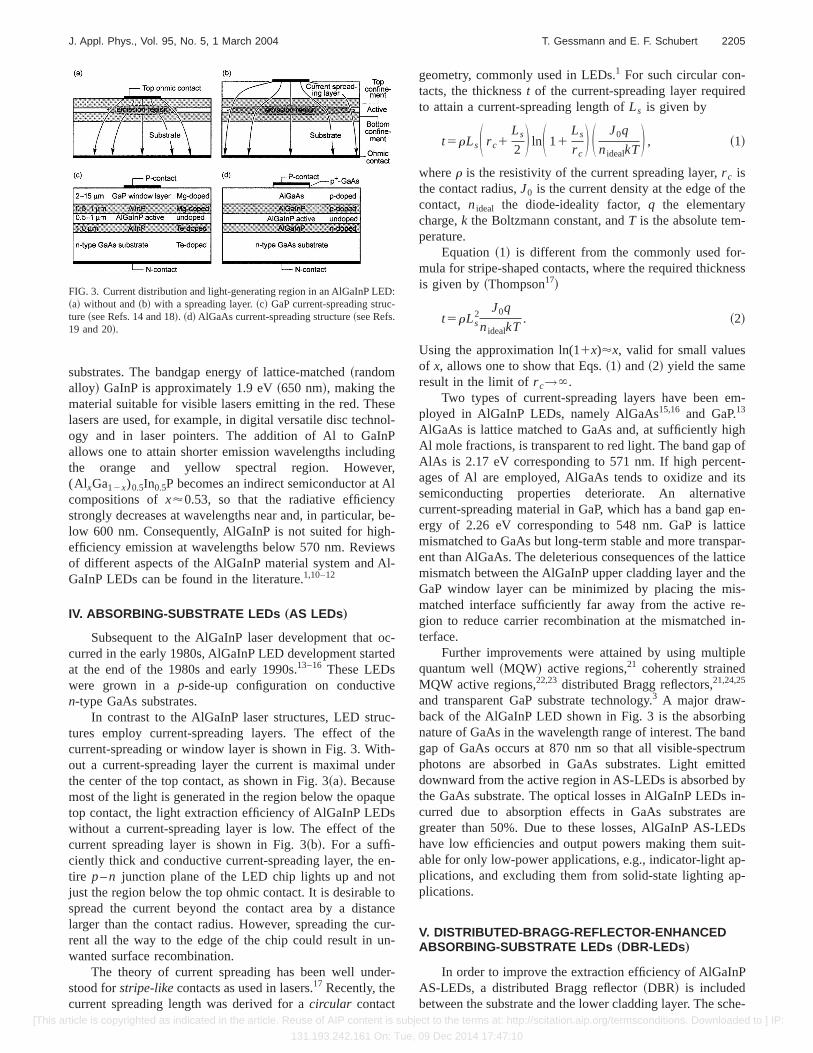
In contrast to the AlGaInP laser structures, LED struc-tures employ current-spreading layers. The effect of thecurrent-spreading or window layer is shown in Fig. 3. With-out a current-spreading layer the current is maximal underthe center of the top contact, as shown in Fig. 3~a!. Becausemost of the light is generated in the region below the opaquetop contact, the light extraction efficiency of AlGaInP LEDswithout a current-spreading layer is low. The effect of thecurrent spreading layer is shown in Fig. 3~b!. For a suffi-ciently thick and conductive current-spreading layer, the en-tire p–n junction plane of the LED chip lights up and notjust the region below the top ohmic contact. It is desirable tospread the current beyond the contact area by a distancelarger than the contact radius. However, spreading the cur-rent all the way to the edge of the chip could result in un-wanted surface recombination.
The theory of current spreading has been well under-stood forstripe-likecontacts as used in lasers.17 Recently, thecurrent spreading length was derived for acircular contact
geometry, commonly used in LEDs.1 For such circular con-tacts, the thicknesst of the current-spreading layer requiredto attain a current-spreading length ofLs is given by
t5rLsS r c1Ls
2 D lnS 11Ls
r cD S J0q
nidealkTD , ~1!
wherer is the resistivity of the current spreading layer,r c isthe contact radius,J0 is the current density at the edge of thecontact, nideal the diode-ideality factor,q the elementarycharge,k the Boltzmann constant, andT is the absolute tem-perature.
Equation~1! is different from the commonly used for-mula for stripe-shaped contacts, where the required thicknessis given by~Thompson17!
t5rLs2 J0q
nidealkT. ~2!
Using the approximation ln(11x)'x, valid for small valuesof x, allows one to show that Eqs.~1! and~2! yield the sameresult in the limit ofr c→`.
Two types of current-spreading layers have been em-ployed in AlGaInP LEDs, namely AlGaAs15,16 and GaP.13
AlGaAs is lattice matched to GaAs and, at sufficiently highAl mole fractions, is transparent to red light. The band gap ofAlAs is 2.17 eV corresponding to 571 nm. If high percent-ages of Al are employed, AlGaAs tends to oxidize and itssemiconducting properties deteriorate. An alternativecurrent-spreading material in GaP, which has a band gap en-ergy of 2.26 eV corresponding to 548 nm. GaP is latticemismatched to GaAs but long-term stable and more transpar-ent than AlGaAs. The deleterious consequences of the latticemismatch between the AlGaInP upper cladding layer and theGaP window layer can be minimized by placing the mis-matched interface sufficiently far away from the active re-gion to reduce carrier recombination at the mismatched in-terface.
Further improvements were attained by using multiplequantum well~MQW! active regions,21 coherently strainedMQW active regions,22,23 distributed Bragg reflectors,21,24,25
and transparent GaP substrate technology.3 A major draw-back of the AlGaInP LED shown in Fig. 3 is the absorbingnature of GaAs in the wavelength range of interest. The bandgap of GaAs occurs at 870 nm so that all visible-spectrumphotons are absorbed in GaAs substrates. Light emitteddownward from the active region in AS-LEDs is absorbed bythe GaAs substrate. The optical losses in AlGaInP LEDs in-curred due to absorption effects in GaAs substrates aregreater than 50%. Due to these losses, AlGaInP AS-LEDshave low efficiencies and output powers making them suit-able for only low-power applications, e.g., indicator-light ap-plications, and excluding them from solid-state lighting ap-plications.
V. DISTRIBUTED-BRAGG-REFLECTOR-ENHANCEDABSORBING-SUBSTRATE LEDs „DBR-LEDs …
In order to improve the extraction efficiency of AlGaInPAS-LEDs, a distributed Bragg reflector~DBR! is includedbetween the substrate and the lower cladding layer. The sche-
FIG. 3. Current distribution and light-generating region in an AlGaInP LED:~a! without and~b! with a spreading layer.~c! GaP current-spreading struc-ture~see Refs. 14 and 18!. ~d! AlGaAs current-spreading structure~see Refs.19 and 20!.
2205J. Appl. Phys., Vol. 95, No. 5, 1 March 2004 T. Gessmann and E. F. Schubert
[This article is copyrighted as indicated in the article. Reuse of AIP content is subject to the terms at: http://scitation.aip.org/termsconditions. Downloaded to ] IP:
131.193.242.161 On: Tue, 09 Dec 2014 17:47:10

matic structure of a DBR-enhanced AS LEDs~here referredto as DBR-LED! is shown in Fig. 4. Katoet al.24 pioneeredDBR-LEDs.
To evaluate the potential enhancement provided by theDBR, it is instructive to determine the DBR reflectivity as afunction of wavelength and angle of incidence. The result ofthis evaluation is shown in Fig. 5 for DBRs designed for anemission wavelength of 630 nm. Two DBRs are shown in thefigure, namely a transparent AlGaInP/AlInP and an absorb-ing AlGaAs/AlGaAs DBR. The transparent DBR has the ad-vantage of low optical losses. However transparency can beattained only by high Al contents in the low-index as well ashigh-index layers, which in turn reduces the refractive indexcontrast. As a consequence, a large number of quarter wavepairs are needed for high reflectivity. On the other hand, theabsorbing DBR allows for a higher index contrast. This en-ables the reduction of the number of quarter wave pairs toattain a certain reflectivity. Thus there is a tradeoff betweennumber of pairs and maximum attainable reflectance in aDBR. Frequently a combination of absorbing and transparentlayers in DBRs is used to maximize the reflectivity and mini-mize the number of quarter wave pairs.
Inspection of Fig. 5~a! reveals a high-reflectivity bandwith a width of more than 50 nm for the transparent DBR;this is wider than the emission linewidth of a typical Al-GaInP LED. Figure 5~b! shows the reflectivity of the DBRsas a function of the angle of incidence. Inspection of thefigure reveals a problematic issue, namely the low reflectiv-ity of the DBR for oblique angles of incidence: For angles20°,f,70°, the DBRs are essentially transparent. Thuslight emitted by the active region in this range of angles canbe transmitted by the DBRs and absorbed in the GaAs sub-strate.
The optical power emitted by the active region into thesolid-angle element given byf andf1df, wheref is as-sumed to be 0° at normal incidence, is given by the propor-tionality
P}r 2 sinf df. ~3!
The sinusoidal dependence indicates that angles near 0°,where the DBR has high reflectivity, have little importance.Angles@0° have greater importance due to the dependenceof the sinus function on angle. However, the DBR has a lowreflectivity in this range of angles, as displayed in Fig. 5.Thus the DBR’s reflectivity characteristics leave substantialroom for improvement. This point will be further discussedin a subsequent section on ODRs.
Figure 5 also shows that the DBR reflectivity increasesagain for grazing-angle incidence, namely forf.70°. As aconsequence, grazing-angle waveguided modes propagatingin the top layers of the LED, namely the confinement, active,and window layers, will be supported by the DBR andguided to the edge of the die where they can escape.
VI. HIGH EXTRACTION STRATEGIES FORAlGaInP LEDs
So far the AlGaInP material system has achieved one ofthe highest internal quantum efficiencies~close to 100% inthe red wavelength range! of all semiconductors used foremission of visible light. It is therefore particularly importantto develop LED structures with extraction efficiencies sig-nificantly exceeding the AS-LED and DBR-LED technolo-gies. General aspects of AlGaInP LED technology have beenthe subjects of several reviews.1,3,4,11Here we briefly reviewcommercially available high extraction efficiency structuresin order to compare them later to the ODR-LEDs.
Early AlGaInP-based LEDs with external efficiencieshsignificantly exceeding GaAsP- and GaP-based devices (h50.1% – 0.6%) were obtained by using organometallic va-por phase epitaxy~OMVPE!. The devices consisted of adouble heterostructure with conductive AlGaAs windowlayers15,16 or conductive GaP-window layers grown latticemismatched with respect to the active region.13 These LEDsattained external quantum efficiencies of about 3% or less inthe wavelength range 555–620 nm (I f520 mA dc).
Subsequently, a twofold increase in quantum efficiencywas achieved by employing a very thick~45 mm! conductiveGaP window layer grown by hydride vapor phase epitaxy ontop of the OMVPE heterostructure.26 The thick window layerallows maximizing the side extraction efficiency, which de-pends on the solid angle of intersection between the windowlayer sidewalls and the cone of acceptance for sideways di-rected light.26 In addition, the thick window layer helps tospread the current beneath the top contact. Peak external ef-ficiencies larger than 6% (I f520 mA dc) have been reportedfor wavelengths.600 nm.26
A. Transparent-substrate LEDs
The devices discussed so far employ the original GaAssubstrate, which absorbs light emitted ‘‘downwards’’ fromthe active region or totally reflected at the LED top surface.This loss effect can be decreased either by covering the
FIG. 4. AlGaInP LED with a distributed Bragg reflector~DBR! locatedbetween the substrate and the lower cladding layer.
FIG. 5. ~a! Reflectivity vs wavelength and~b! reflectivity vs angle of inci-dence for a transparent AlGaInP/AlInP DBR and an absorbing AlGaAs/AlGaAs DBR.
2206 J. Appl. Phys., Vol. 95, No. 5, 1 March 2004 T. Gessmann and E. F. Schubert
[This article is copyrighted as indicated in the article. Reuse of AIP content is subject to the terms at: http://scitation.aip.org/termsconditions. Downloaded to ] IP:
131.193.242.161 On: Tue, 09 Dec 2014 17:47:10

GaAs substrate with a DBR20 or by replacing the GaAs sub-strate with a transparent substrate~TS!.27 Due to the smallrange of angles with high reflectance, the DBR results in adevice which is primarily ‘‘top emitting,’’ whereas a TS de-vice allows for light emission from the edges of the chip andcan therefore be much more efficient.
Similar to double-heterostructure AlGaAs LEDs with atransparent conductive AlGaAs substrate,28 AlGaInP TS-LEDs utilize a transparent conductive GaP carrier. GaP istransparent for the entire range of AlGaInP emission wave-lengths. The use of a conductive substrate supports currentspreading above the patterned backside contacts of theLED.27
AlGaInP transparent substrate~TS! LEDs were pio-neered by Kishet al.27 who developed a technique to removethe original GaAs substrate and to join the LED epitaxiallayer with a conductive GaP carrier by means of directsemiconductor-to-semiconductor waferbonding.27,29,30Figure6 shows the schematic fabrication process, during which asemiconductor–wafer heterointerface is formed. However,the process requires crystallographic alignment, tight controlof all process parameters, and suffers from the use of costlyGaP substrates and increased forward voltages. Furthermore,the current lack of 49 GaP substrates may delay the scalabil-ity of the TS process.
Kish et al.27 reported external quantum efficiencies of17.6% at 629 nm and luminous efficiencies of 41.5 lm/W at604 nm (I f520 mA dc). Further improvements have re-sulted in even higher values of the efficiencies: About 74lm/W at 615 nm and more than 30% external quantum effi-ciency at 632 nm.31
In square-shaped TS-LEDs, several mechanisms limitthe external quantum efficiency such as photon reabsorptionin the active layer and free-carrier absorption in the dopedGaP substrates. In devices withthin active layers~a few na-nometers thick, as generally used in the AlGaAs–InGaAs–GaAs system! reabsorption processes may in factincreasethe external quantum efficiency via photon-recyclingeffects.32 However, due to the low barrier height, AlGaInPdevices with peak wavelengths,630 nm require relativelythick ~several hundred nm! active layers to achieve sufficientelectron confinement and are therefore subject to significantabsorption losses in the active region. For such devices, theexternal efficiency can be increased by geometrically shap-ing the chips so as to minimize the path length of photonsbefore extraction. Suitable chip structures for high extractionefficiencies may be spheres, hemispherical domes, or trun-
cated ellipsoids. However, these structures are difficult torealize and therefore expensive.
Krameset al.33 demonstrated a practical yet very effi-cient structure, the truncated-inverted pyramid~TIP! LEDshown in Fig. 7. The sidewalls of the chip were beveled witha sidewall angle of 35° with respect to the vertical direction~see Fig. 7!. The LED is mountedn-side up on a thermal heatsink in order to enhance heat removal from the device. TheTIP structure redirects photons totally reflected at the side-walls towards the top surface, where they arrive at a moreadvantageous angle and can be extracted. On the other side,photons totally reflected at the top surface can escapethrough the tilted sidewalls@see Fig. 7~b!#.
The performance of AlGaInP TIP-LEDs exceeds 100lm/W at 100 mA dc for emission at 610 nm. Record externalquantum efficiencies of 55% under dc operation (I f
5100 mA) were achieved at 650 nm.33 At the same forwardcurrent under low duty cycle operation, the external quantumefficiency increased to 60.9%, which indicates a lower boundfor the extraction efficiency of the TIP-LED.33
B. Surface-textured LEDs
Chip surfaces may be textured in order to increase thelight extraction efficiency. An advantage of this approach isthat it leads to a scalable chip design as opposed to the chipshaping techniques discussed above. A possibility of struc-turing consists of randomly roughening the upper windowlayer. This can be achieved, e.g., using polystyrene spheresand dry etching.34 In this case, photons incident at the rough-ened surface are either scattered isoptropically~and can es-cape from the chip! or reflected with a random distribution ofthe reflection angles. As a result, the probability of light ex-traction is increased on multiple round trips between surfaceand substrate~assuming the substrate is covered by a high-reflectivity mirror!. To maximize this effect, a highly reflec-tive wide-angle mirror should be inserted between the sub-strate and lower confinement layer; this, however, requires
FIG. 6. Fabrication process of an AlGaInP TS LED. The LED structure iswafer bonded to a GaP substrate~adopted from Ref. 3!.
FIG. 7. TIP-LED structure~from Lumileds Corporation!: ~a! TIP LED un-der operation and~b! typical photon paths and escape possibilities~adoptedfrom Ref. 33!.
2207J. Appl. Phys., Vol. 95, No. 5, 1 March 2004 T. Gessmann and E. F. Schubert
[This article is copyrighted as indicated in the article. Reuse of AIP content is subject to the terms at: http://scitation.aip.org/termsconditions. Downloaded to ] IP:
131.193.242.161 On: Tue, 09 Dec 2014 17:47:10

removal of the original substrate and transfer of the LED toanother carrier. In addition, the thickness of the active regionneeds to be optimized to reduce absorption losses. Externalefficiencies of 46% for GaAS-based LEDs with randomizedsurface structure have been reported.35
Another approach is based onregular patterns of geo-metrical structures on the top surface of the LED~see Fig. 8!.This has been realized using truncated tetrahedrons or othershapes etched into the window layer of an AlGaInPAS-LED.36,37 The two-dimensional pattern of tetrahedronsenhances the effective surface area available to light extrac-tion and offers a variety of surfaces at different tilt angles.Photons entering a single tetrahedron can undergo multipletotal reflection events at the sidewalls guiding them in such away that the incidence angle progressively increases andeventually may fall within the escape cone. However, sincecurrent spreading is strongly obstructed in etched regions, acontact frame on top of the window layers is needed to en-sure uniform current injection across the LED surface. Inaddition, a specially designed wide-angle Bragg reflector isused to recover a large part of the radiation emitted towardsthe substrate side of the LED. For packaged devices emittingat around 610 nm luminous performances larger than 30lm/W and typical operating voltages below 2.2 V have beenachieved.36
C. Photonic-crystal LEDs
Two-dimensional photonic crystals included in the upperwindow layer are examples for periodical structures with acharacteristic length scale of the order of the emitted wave-length. The photonic crystal can be designed to Bragg scatterlight, which is trapped in wave-guided modes, into lightmodes radiating through the top surface. This concept wasused by Erchaket al.38 who demonstrated a sixfold photolu-minescence~PL! intensity increase utilizing a triangular lat-tice etched into the upper window layer of an InGaP/InGaAsLED emitting at 935 nm.
However, nonradiative carrier recombination and surfacerecombination are increased near the etched interfaces. Thiscan pose a problem when the lattice constant of the photonic
crystal becomes comparable to the carrier diffusion length inthe active region. It is therefore important to avoid penetrat-ing the active region with the photonic crystal. While photo-nic crystals in general result in far-field patterns differentfrom flat-surface rectangular-parallelepiped-shaped LEDs,other surface structuring techniques maintain the Lambertianemission pattern.37
D. Thin-film LEDs
An alternative to TS-LEDs, offering high-extraction ef-ficiency, is made possible by TF technology. Here the epitax-ial layer is removed from the original GaAs substrate andtransferred to a another carrier by means of metal-to-metalbonding ~see Figs. 9 and 10!. Stringent semiconductor-to-semiconductor wafer bonding process parameters such as ul-traflat surfaces and crystallographic orientation matching arenot required for TF-LEDs.
Illek et al.39 demonstrated a TF AlGaInP LED with anarray of buried coneshaped microreflectors. The LED struc-ture is shown schematically in Fig. 9. The cones are etchedthrough the active layer and covered by a metal and a thindielectric layer. Small openings in the dielectric provide forelectrical conductivity and localize current injection and lightgeneration to the center of the cones. The shape of the mi-croreflectors is designed such that totally reflected light is
FIG. 8. Top view of surface-textured AlGaInP LEDs with different areas,geometrical patterns, and contact frames~adopted from Ref. 36!. ~a! High-current chip~drive current 400 mA, 5003500mm2 die!. ~b! Low-currentchip ~drive current 30 mA, 2003200mm2 die!. ~c! Standard chip~drivecurrent 70 mA, 3003300mm2 die!.
FIG. 9. ~a! Schematic structure and photograph of~b! uninjected and~c!current-injected AlGaInP thin-film LED with pyramidal microreflectors.Current is injected through the bond pad and a square frame along the edgedof then-type top contact layer. Individualp-type contacts are discernable asdark spots in~b! due to the transparency of the upper window and activelayer ~adopted from Ref. 37!.
FIG. 10. Wafer bonding processing steps for thin film LED technologyutilizing metal-to-metal bonding by means of soldering~adopted from Ref.39!.
2208 J. Appl. Phys., Vol. 95, No. 5, 1 March 2004 T. Gessmann and E. F. Schubert
[This article is copyrighted as indicated in the article. Reuse of AIP content is subject to the terms at: http://scitation.aip.org/termsconditions. Downloaded to ] IP:
131.193.242.161 On: Tue, 09 Dec 2014 17:47:10

guided upwards. As a result, the TF-LED with buried mi-croreflectors is predominantly top emitting. In contrast toTS-LEDs, very thick window layers in order to increasesidelight extraction are not required.37,39For devices emittingat 650 nm, quantum efficiencies of 31%40 and 40%41 havebeen reported. Despite the presence of etched regions, theforward voltage is below 2.0 V at a forward currentI f
510 mA.37,39
There are disadvantages to the TF-LED structure,namely the fact that the ratio of current-injected area to chiparea is small. Analysis of the schematic of Fig. 9~a! and thephotographs of Fig. 9~b! shows that this ratio is less than10%. Furthermore, the microreflectors penetrate the activelayer, thereby subjecting carriers to the possibility of nonra-diative interface recombination.
The semiconductor–metal interface should be highly re-flective and form a low-resistance ohmic contact to the con-ducting carrier. The last requirement can be dropped for TF-LEDs using insulating carriers.42,43 For insulating carriers,two side-by-side top contacts are required. Other importantrequirements are matching of thermal expansion coefficientsbetween the LED epilayer, bonding material and carrier, andgood thermal conductivity of the carrier.
Figure 10 shows a schematic wafer bonding processwhere the LED epilayer covered by a metal such as Au andthe carrier covered by a solder metal such as AuSn arebrought in contact and heated. During this step, during whichthe wafers are kept at low temperatures~350 °C! to avoiddopant redistribution, a stable metal-to-metal bond isformed.37,39This bond is able to sustain all further LED pro-cessing steps including the subsequent removal of the origi-nal substrate by wet-chemical etching.
In order to maximize the extraction efficiency, light ab-sorption at the bonding interface should be minimized andhigh reflectivities should be attained. However, to achievelow contact resistances, an annealing step is required duringwhich the reflectivity of the metal bond may degrade. A thindielectric layer inserted between the semiconductor and thebonding metal helps to avoid thermal degradation of themetal; current flow is enabled through defined openings inthe dielectric.37,39
A distinct advantage of TF technology is the possibilityto structure the AlGaInP surface before the bonding process.This results in a significant increase of the extraction effi-ciency since the geometrical shapes such as cones or spheresact as microreflectors ‘‘buried’’ at the bonding interface be-tween the semiconductor and the carrier.
VII. CONCEPTS FOR REFLECTING STRUCTURES
There are different ways to obtain highly reflective coat-ings in the visible wavelength region. Metallic layers providerobust reflectors capable of reflecting visible light over awide range of wavelengths and incident angles. Metals re-flect visible light since this frequency range is well belowtypical plasma frequencies of the free electron gas. However,electron oscillations induced by incident light waves not onlyresult in reflection but also in absorption caused by electronphonon scattering.
DBRs are periodic structures with a unit cell of two di-electric layers having different refractive indicesni andthicknessesdi( i 51,2). DBRs can be regarded as one-dimensional photonic crystals with a high-reflectivity stopband~‘‘photonic gap’’! comprising the nonpropagating lightstates in the crystal. DBRs are usually designed to have acertain center wavelengthlcenter at perpendicular incidence.However, the DBR reflectivity depends on the incidenceanglef such that the stop band shifts towards shorter wave-lengths for increasingf without changing its spectralwidth.44 As a result, atobliqueincidence angleslcenterlies inmany cases no longer within the high-reflectivity region.
The reflection properties of metals and DBRs also de-pend on the polarization of the incident lightwave. Accordingto Brewster’s law, the reflection of light polarized parallel tothe plane of incidence~TM mode! has a minimum at theincidence angle
tanfB5n1
n2, ~4!
where n1 and n2 are the refractive indices of the adjacentmaterials. This is particularly important for DBRs where theoverall reflectivity significantly decreases atfB . DBRs withimproved wide-angle reflectivity can be achieved, e.g., usingaperiodically stacked layers with thickness gradients or ran-dom thickness distributions.45,46
Much research was devoted to DBRs with a completephotonic band gap represented by a certain frequency rangewhere all incoming photons regardless of their momentumvector \k are reflected. These ODRs have a wide range ofinteresting applications such as all-dielectric coaxialwaveguides,47 omnidirectional mirror fibers,48 and lighttransport tubes.49
Omnidirectional reflection characteristics have been ob-tained using polystyrene and tellurium layers in a DBR.50
Due to the large difference of the refractive indices,npolystyrenene51.8 andntellurium55, the Brewster anglefB ismuch larger than the critical anglefc for total reflectionresulting in a nearly complete photonic band gap in thewavelength range from 10 to 15mm.
Another intriguing approach consists of the use of bire-fringent polymers in DBRs with two different refractive in-dices parallel and vertical to the DBR layer planes.49 Byadjusting the differences between the vertical and in-planeindices the value of the Brewster angle can be controlled.Brewster angles up to 90°~grazing incidence! and evenimaginary values are possible resulting in high reflectivityfor TM-polarized light at virtually all incident angles.
Besides material properties such as the radiative recom-bination efficiency10 one of the most important figures-of-merit for LEDs is the extraction efficiencyhextractiondefinedas the number of photons emitted into open space relative tothe number of photons generated in the active region.
The value ofhextraction is limited by the fact that lightemitted from the active region may be subjected to totalreflection at the LED surface~see Fig. 11!. The critical anglefc for total reflection is given by Snell’s law
2209J. Appl. Phys., Vol. 95, No. 5, 1 March 2004 T. Gessmann and E. F. Schubert
[This article is copyrighted as indicated in the article. Reuse of AIP content is subject to the terms at: http://scitation.aip.org/termsconditions. Downloaded to ] IP:
131.193.242.161 On: Tue, 09 Dec 2014 17:47:10

sinfc5nout
ns, ~5!
wherens andnout denote the refractive indices of the semi-conductor and the outside medium, respectively.
As an example, the AlGaInP material system has a valueof fc'17° with air as outside medium which in turn meansthat about 96% of the light emitted from the active region isreflected at the surface~we usedns53.4 atl5650 nm forGaP as the semiconducting material!. This value can be re-duced to about 88% by embedding the LED in epoxies withhigh refractive indices ofnepoxy'1.5.3
Distributed Bragg reflectors can be used as substratecoating to enhance the light extraction.24,51 However, the ac-tive region of a LED emits light isotropically and therefore
the poor DBR reflectivity at oblique incidence angles resultsin undesired losses particularly for waveguided modes asdiscussed above.
Unfortunately the applicability of the above-mentionedomnidirectional DBRs in LEDs is limited since they are elec-trically insulating. In addition, these DBR structures presenta considerable thermal barrier preventing efficient heat sink-ing due to their large thermal resistance combined with largethickness.
VIII. OMNIDIRECTIONAL REFLECTOR „ODR…
FOR LEDs
Here we describe a very promising omnidirectional re-flector suitable for use in future large-area LEDs.52 The re-flector comprises the LED semiconductor material emittingat a wavelengthl0 , a low-refractive index layer (nli ) , and ametal with a complex refractive indexNm5nm1 ikm asshown in Fig. 12.
At perpendicular incidence, the reflectance of the triple-layer ODR is given by
RODR~f50!5$~nS2nli !~nli1nm!1~nS1nli !km%21$~nS2nli !km1~nS1nli !~nli2nm!%2
$~nS1nli !~nli1nm!1~nS2nli !km%21$~nS1nli !km1~nS2nli !~nli2nm!%2 . ~6!
Equation~6! is calculated for a phase thickness of the low-index layer corresponding tol0 /(4 nli ) ~‘‘quarter wavelayer’’!. For an AlGaInP/SiO2 /Ag structure emitting atl5630 nm, Eq. ~6! yields a normal-incidence reflectanceRODR(u50).98%. This value exceeds the correspondingvalue for a structure without low-index layer by about 3%,thereby reducing optical losses by a substantial amount.
The omnidirectional reflection characteristics can be at-tributed to an imaginary interfacial Brewster anglefB simi-lar to the birefringent DBRs. For an ODR consisting of just asemiconductor and a metal layer, the Brewster angle is givenby
tanfB5nm
ns1 i
km
ns. ~7!
An analogous relationship is valid if an intermediate di-electric layer is used. The magnitude of the imaginary part inEq. ~7! determines how strongly the reflectivity decrease ofTM-polarized light atfB is suppressed. As can be inferredfrom Eq. ~7!, a criterion to maintain high reflectivity is tomaximizekm /ns and minimizenm /ns . In an AlGaInP-basedLED (ns53.3) emitting atl5630 nm silver (nm50.08,km
54) is a particularly good choice as compared to other met-als such as gold (nm50.18,km52.4) or nickel (nm52.1,km
53.6).Figure 13 compares different triple-layer ODRs to a
transparent DBR widely used in AlGaInP-based LEDs.While the ODRs maintain high reflectivity at virtually all
FIG. 11. Schematic of a standard AS-LED incorporating a DBR. Light raystotally reflected at the surface and the DBR are indicated in red.
FIG. 12. Perspective view of the ODR. In the ODR-LED, the ODR servesas ohmic contact.
FIG. 13. Calculated reflectivity for two ODRs and a DBR with a centerwavelength at 630 nm. GaP was chosen as the external medium. The trans-parent AlGaInP DBR consists of 35@(Al0.3Ga0.7)0.5In0.5P/Al0.5In0.5P# pairs.The ODRs have a 500 nm thick metal layer covered by a quarter wave thickSiO2 layer on a GaAs substrate:~a! reflectivity vs wavelength for normalincidence and~b! angular dependence of the reflectivity at 630 nm. Thesolid and dashed lines correspond to transverse electric and transverse mag-netic polarized waves, respectively.
2210 J. Appl. Phys., Vol. 95, No. 5, 1 March 2004 T. Gessmann and E. F. Schubert
[This article is copyrighted as indicated in the article. Reuse of AIP content is subject to the terms at: http://scitation.aip.org/termsconditions. Downloaded to ] IP:
131.193.242.161 On: Tue, 09 Dec 2014 17:47:10

angles of incidence, the DBR reflectivity sharply dropsabove 17°. The curves shown in Fig. 13 were calculatednumerically using the optical transfer-matrix method.44 It canbe inferred from Fig. 13 that triple-layer ODRs perform sig-nificantly better at oblique angles of incidence than transpar-ent DBRs. This illustrates the substantial gain brought aboutby the use of ODRs in LEDs.
The ODR described here can be used with low-cost Sisubstrates using conductive epoxy or by means of a metal-to-metal bonding process. These bonding processes havemuch less stringent requirements than direct semiconductor-to-semiconductor wafer bonding processes as used for TS-LEDs. The schematic structure of the ODR-LED is shown inFig. 14. It consists of a top current-spreading~or window!layer, the active and confinement layers, a bottom windowlayer, the ODR, and a submount such as a Si or metal wafer.The active layers include the lower and upper confinementlayers and the bulk or MQW active region. The wafer isgrown in the standard ‘‘p-side up’’ mode that is employed innearly all AlGaInP LEDs at the present time.
As shown in Fig. 14, the low-index layer is perforated bymany small ohmic contacts that cover only a small fractionof the entire backside area of the LED die. The array ofmicrocontacts allows the electrical current to pass throughthe dielectric layer. Assuming that the ohmic contacts havean area of 1% of the die, and that the alloyed ohmic contactmetal is 50% reflective, the reflectivity of the ODR is re-duced by only 0.5%.
Because the LED active region emits light isotropically,the total substrate reflectivity averaged over the solid anglewould be a suitable figure-of-merit. The average reflectivityis given by
R̄~l!51
2p E0
p/2
R~l,f!2p sinfdf, ~8!
wherel denotes the emission wavelength andf the angle ofincidence. Values ofR̄ for different reflectors are calculatedby numerical integration of the reflectivity curves shown inFig. 13 and are listed in Table I. The averaged reflectivity oftriple-layer ODRs exceeds the value ofR̄ for the transparentDBR by about a factor of 2. A reflectivity gain by a factor of2.1 is obtained for the Ag–SiO2 ODR.
Note that the reflectivity increase is significant and sub-stantial. For a loss less medium, the power of a waveguidedmode,P, attenuated by multiple reflection events~with re-flectivity R! depends on the number of reflection events,N,according to
P5P0RN, ~9!
where P0 is the initial power of the mode. This equationillustrates thatR is of great importance due to the power-lawdependence. High values ofR are essential to minimizewaveguide losses. This consideration shows the tremendousadvantage offered by ODRs.
The wide-angle reflectivity of the ODR allows waveguiding of light rays with much smaller attenuation than aDBR. As a result, light extraction at the edges of the LEDchip is strongly increased. In addition, the top surface of theODR-LED may be rougher than the surface of the DBR-LED due to the etching used for the substrate removal. As-suming random surface roughness, photons are either scat-tered isotropically or totally reflected with a randomdistribution of reflection angles. As a result, photon outcou-pling from waveguided modes into vertical radiation modesis drastically enhanced during round trips between the sur-face and ODR.
IX. CHARACTERISTICS OF ODR-LEDs
The ODR-LED technology does not exhibit the opticallosses of AS-LEDs and DBR-LEDs due to the employmentof a high-reflectivity omnidirectional reflector. Therefore asignificant performance advantage for ODR-LED comparedwith AS-LEDs and DBR-LEDs can be obtained.
Figure 15 compares the current injection patterns forAS-, TS-, and ODR-LEDs. Inspection of the figure revealsthat both AS and TS technologies have maximum currentdensity under the top contact. Since the top contact is opaqueand has low reflectivity, light generated below the contact is
FIG. 14. Schematic of the ODR-LED. An array of microcontacts perforatingthe ODR serves asp-type ohmic contact to the epitaxial AlGaInP layers.
FIG. 15. Current distribution and size of light-emitting region in AS-, TS-,and ODR-LEDs. ‘‘1’’ denotes the current spreading layer and ‘‘2’’ the regionof light emission.
TABLE I. Values of the angle-integrated reflectivityR̄ at 630 nm calculatedfrom Eq. ~8! using the theory curves such as shown in Fig. 13~b!. Themetal–ODRs consist of a 500 nm thick metal layer covered by a quarterwave SiO2 layer on a GaAs substrate. The transparent AlGaInP–DBR con-sists of 35@(Al0.3Ga0.7)0.5In0.5P/Al0.5In0.5P# quarter wave pairs. The valuesof nm , n1 , nh correspond to the refractive indices of the metals and thelow-/high-index layers in the DBRs,km denotes the metal-extinction coef-ficient. GaP was chosen as outside medium for all reflectors (nS53.3 forGaP atl5630 nm).
Reflector typeRefractive index
(l5630 nm)Extinction coefficient
(l5630 nm)R̄
(l5630 nm)
Ag–SiO2 ODR nm50.08 km54 0.994Au–SiO2 ODR nm50.18 km52.7 0.962Ni–SiO2 ODR nm52.1 km53.6 0.932AlGaInP–DBR n152.9, nh53.35 Transparent 0.473
2211J. Appl. Phys., Vol. 95, No. 5, 1 March 2004 T. Gessmann and E. F. Schubert
[This article is copyrighted as indicated in the article. Reuse of AIP content is subject to the terms at: http://scitation.aip.org/termsconditions. Downloaded to ] IP:
131.193.242.161 On: Tue, 09 Dec 2014 17:47:10

blocked. The ODR-LED avoids these optical losses due to apatterned backside contact that results in a current injectionpattern minimizing the current flow under the top contact.Patterning of the backside contact wouldnot be effectivetoAS- and TS-LEDs because the highly conductive substrates~GaAs and GaP! effectively spread the current along lateraldirections.
The comparison of the AS and TS current–voltage(I –V) characteristics shown in Fig. 16 illustrates that TS-LEDs have a slightly higher forward voltage. The hetero-junction band discontinuity occurring at the semiconductor-to-semiconductor wafer-bonded interface, low doping of theGaP substrate~to avoid free-carrier absorption!, and interfa-cial oxides are possible reasons for the forward-voltage pen-alty in TS-LEDs. As a result of the higher forward voltage,the electrical input power increases and the luminous perfor-mance is reduced. For ODR-LEDs no such forward-voltagepenalty is expected.
The Si or metal submounts employed in the ODR-LEDhave a high thermal conductivity. This can be seen in TableII, which compares the thermal conductivity of GaAs, GaP,Si, Cu, and sapphire. Even though metal substrates havemuch higher thermal conductivity than any semiconductor,the higher thermal conductivity of Si submounts will alreadyallow for lower active region temperatures and thus higherdrive currents as compared to the GaAs or GaP. In addition,the greater mechanical stability of Si wafers will enable thin-ner submounts as compared to TS or AS devices, thus allow-ing for improved heat sinking. The low-index dielectric layerused for the ODR has a negligible influence on the thermalconductance due to its small thickness@l/(4n)'110 nm#.
Electroluminescence spectra of an Ag-based ODR-LEDattached to a conductive Si substrate with silver epoxy and a
TS-LED emitting at 595 nm are shown in Fig. 17. The spec-tra were measured at two different drive current values inorder to study the effect of active region heating on bothdevices. Devices were isolated by wet-chemical etching~ODR-LED! or cleaved from the wafer~TS-LED! with junc-tions areasAj'0.05 mm2 ~TS-LED! and Aj'0.09 mm2
~ODR-LED!. In the heating experiment the drive current waschosen such that the current densities in the two devices werecomparable assuming uniform current distribution across thejunction area. The slope of the high-energy side of the elec-troluminescence band is proportional to
intensity}exp@2~hn/kT!#. ~10!
As the straight-line fits in Fig. 17 show, the slope indeedbecomes smaller with increasing drive current indicating atemperature rise of the active region. This change is morepronounced for the TS-LED indicating stronger heating ofthe device.
The lower device heating of the ODR-LED can be at-tributed to the higher thermal conductivity of the Si sub-strate. However, it is important to note that the heating ofAlGaInP LEDs increases towards shorter emission wave-lengths. This is caused by the decreasing confinement barrierheight allowing more carriers to leave the active region andthe resulting lower internal radiative efficiency. The thermalconductivity of Si is about 300% larger than in GaAs andabout 50% higher than in GaP. As a result, the active regionis less heated in ODR-LEDs as compared to AS- and TS-LEDs. This is an important feature for high-power LEDssince it allows operating ODR devices at higher injectioncurrents and higher optical power levels. In addition, Si sub-strates are available at much lower cost than compoundsemiconductor substrates.
Micrographs of an Ag-based ODR-LED under externalillumination and under operation are shown in Figs. 18~a!and 18~b!, respectively. The emission occurs in the red partof the spectrum with a peak wavelength of 650 nm. Thepattern of small-area ohmic contacts beneath the large areatop contacts can be clearly seen. In Fig. 18~a!, the small-areacontacts appear dark because their reflectivity is lower than
FIG. 16. Current vs voltage characteristic of an AS-LED and a TS-LED.
FIG. 17. Electroluminescence spectra of an ODR-LED (l5650 nm) and aTS-LED (l5595 nm) measured at different values of the drive currentdensityJ. The slope of the high-energy side of the electroluminescence peakis proportional to the active region temperature. The straight lines are fits tothe experimental data.
TABLE II. Thermal conductivity of GaAs, GaP, Si, Cu, and sapphire atroom temperature.
Material GaAs GaP Si Cu Sapphire
Thermal conductivity W/~cm K! 0.5 1.1 1.5 3.85 0.35
2212 J. Appl. Phys., Vol. 95, No. 5, 1 March 2004 T. Gessmann and E. F. Schubert
[This article is copyrighted as indicated in the article. Reuse of AIP content is subject to the terms at: http://scitation.aip.org/termsconditions. Downloaded to ] IP:
131.193.242.161 On: Tue, 09 Dec 2014 17:47:10

the reflectivity of the surrounding ODR. In Fig. 18~b!, how-ever, the small contacts are brighter indicating light emissionin their vicinity.
Optical output powerP versus injection currentI for anAg ODR-LED bonded with silver epoxy to conductive Si, anAS-LED with a DBR, and a TS-LED are shown in Fig. 19.The peak wavelengths of the three devices are 650 nm~ODR-LED!, 630 nm ~DBR-LED!, and 595 nm~TS-LED!with junction areasAj'0.09, 0.25, and 0.05 mm2, respec-
tively. In order to measure the total optical output power thesamples were placed on a reflecting holder inside an integrat-ing sphere.
The largest light output is attained by the ODR-LED.Maximum values of the external quantum efficiencieshext
are about 18% for the ODR device (I f527 mA), 11% forthe DBR-LED (I f527 mA), and 12% for the TS-LED (I f
511 mA). TS-LEDs operating at 632 nm have an excellentexternal efficiency of 32%,31 about a factor of 2 higher thanthe ODR-LED shown in Fig. 19. The external quantum effi-ciency of the ODR device is expected to further increasewith a thicker top window layer. The window layer thicknessof the ODR device shown in Fig. 19 is 2.0mm and it isreasonable to expect an improvement by a factor of 2 foroptimized ODR devices with a thick window layer.
In the linear region of the light-output-power versus cur-rent curves of Fig. 19 the DBR-LED emits clearly the small-est optical power even though it has a larger internal effi-ciency than the TS-LED corresponding to its longer emissionwavelength. This is direct evidence of the high extractionefficiency of transparent substrate devices.~An AS-LEDwithout the DBR has even lower output power than theDBR-LED and is therefore not shown in the figure!.
Inspection of Fig. 19 shows that the saturation of theoptical output power is smallest for the ODR-LED. The satu-ration may be caused by carrier overflow over the confine-ment barriers. Taking into account the differences in thejunction areasAj of the ODR- and AS-LED this can be at-tributed to the better thermal conductivity of the Si holder ascompared to GaAs. The pronounced saturation effect in theTS-LED is likely caused by the smaller confinement barrierheight allowing more carriers to flow over the barrier.
Figure 20 compares the external quantum efficiencieshe
of the TS, AS, and ODR-LED to values obtained for othermaterial systems in particular to AlGaInP-based LEDs with athick window layer. Even in the present state the externalquantum efficiency of the ODR-LED is about 1.6 timeslarger thanhext of the DBR-LED.
FIG. 18. ~a! Micrograph of an AlGaInP ODR-LED with Ag reflector bondedwith silver epoxy to conductive Si under external illumination.~b! Micro-graph of the same ODR-LED with current injection (I 520 mA).
FIG. 19. Dependence of the total optical output power on the drive currentfor AlGaInP LEDs with different emission wavelengthsl and junction areasAj . The samples were placed on a reflective sample holder inside an inte-grating sphere for the measurements. The data for the red TS-LED are takenfrom Ref. 33.
FIG. 20. External quantum efficiency for different LEDs. Data points arelabeled with epitaxial material and the substrate~epi/substrate!. ~Data takenfrom Refs. 26, 33, 41, and this work.!
2213J. Appl. Phys., Vol. 95, No. 5, 1 March 2004 T. Gessmann and E. F. Schubert
[This article is copyrighted as indicated in the article. Reuse of AIP content is subject to the terms at: http://scitation.aip.org/termsconditions. Downloaded to ] IP:
131.193.242.161 On: Tue, 09 Dec 2014 17:47:10

The I –V characteristic of an AlGaInP ODR-LED isshown in Fig. 21. At a current of 20 mA, the forward voltageis about 2.7 V. For comparison, theI –V characteristics of anAlGaInP DBR-LED and TS-LED are also shown in the fig-ure. It should be noted that theI –Vs of DBR- and ODR-LEDs do not result from optimized processes or optimizedtop layers for low-ohmic contact resistances as in the case ofthe TS device.
X. WAFER BONDING FOR AlGaInP ODR-LEDs
Two fabrication routes for AlGaInP-based ODR LEDs~n-type up orp-type up! are shown schematically in Figs. 22and 23. Both processes start out with ‘‘p-side up’’ epiwafers,which are the standard for epitaxial growth, and includefront- and backside processing of the ODR-LED, removal ofthe original substrate, and bonding to a conductive carrier.The conductive carrier should ensure good heat sinking andshould be thermal-expansion matched with respect to the ep-ilayer.
The p-type up process involves more steps~due to theuse of a temporary holder!, but has the potential for lowercontact resistances at the LED backside contact since thesmall-area contact pattern is applied ton-type material. Then-type up process does not require a temporary holder butthe backside ohmic contacts are top-type material, whichlikely results in higher contact resistances.
Chemo-mechanical polishing can be employed to thinthe GaAs wafer down to a thickness of about 50–100mm.The remaining layer can then be removed by selective wetchemical etching. The wet-chemical etching step, however,requires one or more etch stop layers covering the bottom
window layer of the LED to prevent etch damage. With op-timized thickness, composition, and sequence of several etchstop layers the damage to the lower window layer can beminimized.
The epitaxial ODR LED layer needs to be bonded to apermanent holder. Several materials are suited as holders: Siand metal substrates have high thermal conductivity whencompared to GaAs or GaP and therefore provide for efficientheat sinking. However, suitable holder materials have to en-sure thermal expansion matching, which is required to avoidstress damage to the LED during processing steps at elevatedtemperatures.
The bonding process has to result in a uniform large-areabond between the substrate and the LED, which is able tosustain temperature cycling required during further LED pro-cessing such as annealing of electrical contacts. Furthermore,the wafer bonding process should be compatible with a 4 in.process.
The bond may be accomplished by forming a binaryintermetallic compound located between the conductiveholder and the LED epilayer. For this purpose, the bondingsurfaces may be covered either directly with the alloy53 orwith the two separate components in a layer sequence withindividual thicknesses ensuring the correct alloycomposition.54,55 Subsequently the two surfaces are stackedface-to-face and annealed. The bonding is mediated by solidphase reactions such as solid-phase epitaxial regrowth at thealloy/epilayer and the alloy/holder interfaces. Preferably, italso involves liquid-phase reactions that help to reduce sur-face roughness.54,55 The bonding material should adhere tothe LED epilayer as well as to the holder and should havelow electrical resistance. The bonding process should takeplace at sufficiently low temperatures in order to avoid dop-ant redistribution in the heterostructure. Note that the re-quirements for the bonding process discussed above are lesscritical than for the semiconductor-to-semiconductor bond-ing processes used in TS technology.
As an example, the AuGe intermetallic compound is ca-pable of forming low-resistivity contacts ton-type GaAs andcan therefore be employed to bond the ODR-LED epilayer toa GaAs holder. AuGe forms a eutectic phase during thebonding process at temperatures close to the melting pointTm5360 °C of the eutectic. Other systems such as PdIn with
FIG. 21. Current vs voltage characteristics for ODR-, DBR-, and TS-LEDsemitting at 650, 630, and 595 nm, respectively. The junction areasAj areabout 0.09 mm2 for ODR- and AS-LEDs and about 0.05 mm2 for the TS-LED.
FIG. 22. Schematic process for a ‘‘p-type up’’ ODR light-emitting diode.After epitaxial growth~a!, large areap-type contacts are applied to the frontside of the ODR-LED~b!. The wafer is then attached to a temporary topholder by means of wax or a similar substance; after removal of the originalsubstrate, then-type microcontact pattern with dielectric and metal reflectoris defined on the backside of the ODR LED~c!. Finally, the wafer is bondedto a conductive permanent holder~d!.
FIG. 23. Schematic process for ann-type up ODR light-emitting diode.After epitaxial growth~a!, the p-type microcontact pattern with dielectricand metal layers is defined on the backside of the ODR LED~b!. The waferis then bonded to the conductive carrier~c!. Finally, the original substrate isremoved and large arean-type contacts are applied to the front side of theODR-LED ~d!, ~e!.
2214 J. Appl. Phys., Vol. 95, No. 5, 1 March 2004 T. Gessmann and E. F. Schubert
[This article is copyrighted as indicated in the article. Reuse of AIP content is subject to the terms at: http://scitation.aip.org/termsconditions. Downloaded to ] IP:
131.193.242.161 On: Tue, 09 Dec 2014 17:47:10

a transient liquid phase have been used for bonding of GaNepilayers to Si.54,55
An alternate possibility to permanently bond the epilayerto a holder is the use of silver-loaded epoxy. The epoxyoffers excellent electrical conductivity, adhesion, and bondstrength. It can be easily and uniformly dispensed on thesample and is extremely reliable. However, during subse-quent contact annealing the degradation temperature of theepoxy polymerTD'400 °C must not be exceeded. In addi-tion, the thermal expansion is different from GaP and there-fore thermal expansion matching is difficult.
XI. CONCLUSIONS
In this review AlGaInP structures suited for LEDs oper-ating in the red, orange, yellow, and yellow–green wave-length range were discussed. These devices will play a keyrole in solid-state lighting applications. One of the most im-portant requirements for use of LEDs in solid-state lightingis the attainment of very large light extraction efficiencies.For this reason this review placed particular emphasis ondevice structures allowing for high-brightness light emission.These structures overcome the inherent light loss due to theabsorbing GaAs substrate in standard AlGaInP LEDs by ei-ther replacing GaAs with a transparent GaP carrier or bycovering it with reflectors. TS LEDs have attained recordexternal quantum efficiencies of 55% exceeding the effi-ciency of AS LEDs by a factor of 10. However, their cost ofmanufacturing is high due to the employment of GaP sub-strates, a critical wafer-bonding process, and a thick GaPwindow layer.
LEDs employing a DBR inserted between the GaAs sub-strate and the lower window layer are widely used types ofreflector-enhanced devices. These DBR-LEDs offer higherlight extraction efficiencies than AS-LEDs, yet they areplagued by the fact that the excellent reflective properties ofDBRs are limited to vertically incident light. These draw-backs are avoided by TS-LEDs and TF-LEDs, which utilizemetal-to-metal wafer fusion techniques and attained largequantum efficiencies as high as 40%.
The recently developed high-reflectivity, electricallyconductive ODRs are able to considerably outperform con-ventional DBR’s. The ODR can be integrated as ap-typecontact into an AlGaInP-based LED emitting at 650 nm. Af-ter removal of the original GaAs substrate using mechanicalpolishing and wet-chemical etching, the ODR LED ismounted on a conductive Si with silver-loaded epoxy. TheODR-LED has been compared to an AlGaInP-based LEDwith a conductive DBR covering the GaAs substrate~DBR-LED!. From measurements of the optical output power ver-sus forward current external quantum efficiencies of about18% and 11% have been obtained for ODR- and AS-LED,respectively. In addition, the Si substrate has superior heatconductivity compared to GaAs and GaP substrates and al-lows operating the device at potentially high current densityand light output levels. Different generic methods can beutilized to increase light extraction of all the device struc-tures mentioned above. As examples, techniques to patternLED surfaces with random or regular structures in particular
with photonic crystals have been presented. Shaping of theentire chip has proven extremely beneficial in the case ofTS-LEDs and enabled the record efficiencies obtained bythese devices.
AlGaInP LEDs are extremely promising devices forhigh-power solid-state lighting applications. In particular,high-brightness red LEDs using ODRs can be employed inhigh-efficiency trichromatic and tetrachromatic white lightsources. This will enable production of white light with highcolor rendering indexes in future solid-state lighting applica-tions.
1E. F. Schubert,Light Emitting Diodes~Cambridge University Press, Cam-bridge, U.K., 2003!.
2F. M. Steranka, inHigh Brightness Light Emitting Diodes, edited by G. B.Stringfellow and M. G. Craford, Semiconductors and Semimetals Vol. 48~Academic, San Diego, 1997!, pp. 65–95 and references therein.
3F. A. Kish and R. M. Fletcher, inHigh Brightness Light-Emitting Diodes,edited by G. B. Stringfellow and M. G. Craford, Semiconductor and Semi-metals, Vol. 48~Academic, San Diego, 1997!, pp. 149–220 and referencestherein.
4C. H. Chen, S. A. Stockman, M. J. Peanasky, and C. P. Kuo, inHighBrightness Light Emitting Diodes, edited by G. B. Stringfellow and M. G.Craford, Semiconductors and Semimetals, Vol. 48~Academic, San Diego,1997!, pp. 97–144 and references therein.
5Y.-L. Li, Th. Gessmann, and E. F. Schubert, Proceedings SPIE AnnualMeeting, San Diego, August 4–8, 2003.
6K. Kobayashi, S. Kawata, A. Gomyo, I. Hino, and T. Suzuki, Electron.Lett. 21, 931 ~1985!.
7Y. Ohba, M. Ishikawa, H. Sugawara, T. Yamamoto, and T. Nakanisi, J.Cryst. Growth77, 374 ~1986!.
8M. Ikeda, K. Nakano, Y. Mori, K. Kaneko, and N. Watanabe, J. Cryst.Growth 77, 380 ~1986!.
9K. Itaya, M. Ishikawa, and Y. Uematsu, Electron. Lett.26, 839 ~1990!.10See, for example,High Brightness Light-Emitting Diodes, edited by G. B.
Stringfellow and M. G. Craford, Semiconductors and Semimetals, Vol. 48~Academic, San Diego, 1997!.
11See, for example,Electroluminescence I, edited by G. Mueller, Semicon-ductors and Semimetals, Vol. 64~Academic, San Diego, 2000!.
12M. R. Krames, H. Amano, J. J. Brown, and P. L. Heremans, IEEE J. Sel.Top. Quantum Electron.8, 185 ~2002!.
13C. P. Kuo, R. M. Fletcher, T. D. Osentowski, M. C. Lardizabel, M. G.Craford, and V. M. Robbins, Appl. Phys. Lett.57, 2937~1990!.
14R. M. Fletcher, C. P. Kuo, T. D. Osentowski, and V. M. Robbins, USPatent No. 5,008,718~1991!.
15H. Sugawara, M. Ishikawa, and G. Hatakoshi, Appl. Phys. Lett.58, 1010~1991!.
16H. Sugawara, M. Ishikawa, Y. Kokubun, Y. Nishikawa, and S. Naritsuka,U.S. Patent No. 5,048,035~1991!.
17G. H. B. Thompson,Physics of Semiconductor Laser Devices~Wiley,New York, 1980!.
18R. M. Fletcher, C. P. Kuo, T. D. Osentowski, K. H. Huang, and M. G.Craford, J. Electron. Mater.20, 1125~1991!.
19H. Sugawara, M. Ishakawa, Y. Kokubun, Y. Nishikawa, S. Naritsuka, K.Itaya, G. Hatakoshi, and M. Suzuki, United States Patent No. 5,153,889~1992!.
20H. Sugawara, K. Itaya, H. Nozaki, and G. Hatakoshi, Appl. Phys. Lett.61,1775 ~1992!.
21K.-H. Huang and T.-P. Chen, U.S. Patent No. 5,661,742~1997!.22S. J. Chang and C. S. Chang, IEEE Photonics Technol. Lett.10, 772
~1998!.23S. J. Chang and C. S. Chang, Jpn. J. Appl. Phys., Part 237, L653 ~1998!.24T. Kato, H. Susawa, M. Hirotani, T. Saka, Y. Ohashi, E. Shichi, and S.
Shibata, J. Cryst. Growth107, 832 ~1991!.25S. J. Chang, C. S. Chang, Y. K. Su, P. T. Chang, Y. R. Wu, K. H. Huang,
and T. P. Chen, IEE Proc.: Optoelectron.144, 1 ~1997!.26K.-H. Huang, J. G. Yu, C. P. Kuo, R. M. Fletcher, T. D. Osentowski, L. J.
Stinson, M. G. Craford, and A. S. H. Liao, Appl. Phys. Lett.61, 1045~1992!.
27F. A. Kish et al., Appl. Phys. Lett.64, 2839~1994!.28L. W. Cook, M. D. Camras, S. L. Rudaz, and F. M. Steranka, inProceed-
2215J. Appl. Phys., Vol. 95, No. 5, 1 March 2004 T. Gessmann and E. F. Schubert
[This article is copyrighted as indicated in the article. Reuse of AIP content is subject to the terms at: http://scitation.aip.org/termsconditions. Downloaded to ] IP:
131.193.242.161 On: Tue, 09 Dec 2014 17:47:10

ings of the 14th International Symposium on GaAs and related Com-pounds 1987~Institute of Physics, Bristol, 1988!, pp. 777–780.
29F. A. Kish, D. A. Vanderwater, M. J. Peanasky, M. J. Ludowise, S. G.Hummel, and S. J. Rosner, Appl. Phys. Lett.67, 2060~1995!.
30G. E. Hoefler, D. Vanderwater, D. C. DeFevere, F. A. Kish, M. Camras, F.Steranka, and I.-H. Tan, Appl. Phys. Lett.69, 803 ~1996!.
31N. F. Gardneret al., Appl. Phys. Lett.74, 2230~1999!.32M. Boroditsky and E. Yablonovitch, Proc. SPIE3002, 119 ~1997!.33M. R. Krameset al., Appl. Phys. Lett.75, 2365~1999!.34H. W. Deckman and J. H. Dunsmuir, Appl. Phys. Lett.41, 377 ~1982!.35R. Windischet al., Appl. Phys. Lett.79, 2315~2001!.36N. Linder, S. Kugler, P. Strauss, R. Wirth, H. Zull, and K. P. Streubel,
Compound Semicond.7, 59 ~2001!.37K. Streubel, N. Linder, R. Wirth, and A. Jaeger, IEEE J. Sel. Top. Quan-
tum Electron.8, 321 ~2002!.38A. Erchak, D. J. Ripin, S. Fan, P. Rakich, J. D. Joannopoulos, E. P. Ippen,
G. S. Petrich, and L. A. Kolodziejski, Appl. Phys. Lett.78, 563 ~2002!.39S. Illek, U. Jacob, A. Ploessl, P. Strauss, K. Streubel, W. Wegleiter, and R.
Wirth, Compound Semicond.8, 39 ~2002!.40C. Rooman, S. De Jonge, C. Karnutsch, K. P. Streubel, M. Kuijk, B. Dutta,
G. Borghs, and P. L. Heremans, Proc. SPIE4996, 40 ~2003!.41R. Wirth et al., Proc. SPIE4996, 1 ~2003!.42R. H. Horng, D. S. Wuu, S. C. Wei, M. F. Huang, K. H. Chang, P. H. Liu,
and K. C. Lin, Appl. Phys. Lett.75, 154 ~1999!.43R. H. Horng, D. S. Wuu, S. C. Wei, C. W. Tseng, M. F. Huang, K. H.
Chang, P. H. Liu, and K. C. Lin, Appl. Phys. Lett.75, 3054~1999!.44H. A. Macleod, Thin-Film Optical Filters ~McGraw-Hill, New York,
1986!, pp. 35–45.45K. V. Popov, J. A. Dobrowolski, A. V. Tikhonravov, and B. T. Sullivan,
Appl. Opt. 36, 2139~1997!.46J. Xu, H. Fang, and Zh. Lin, J. Phys. D34, 445 ~2001!.47M. Ibanescu, Y. Fink, S. Fan, E. L. Thomas, and J. D. Joannopoulos,
Science289, 415 ~2000!.48S. D. Hart, G. R. Maskaly, B. Temelkuran, P. H. Prideaux, J. D. Joannopo-
ulos, and Y. Fink, Science296, 510 ~2002!.49M. F. Weber, C. A. Stover, L. R. Gilbert, T. J. Nevitt, and A. J. Ouderkirk,
Science287, 2451~2000!.50Y. Fink, J. N. Winn, S. Fan, Ch. Chen, J. Michel, J. D. Joannopoulos, and
E. L. Thomas, Science282, 1679~1998!.51S. W. Chiou, C. P. Lee, C. K. Huang, and C. W. Chen, J. Appl. Phys.87,
2052 ~2000!.52Th. Gessmann, E. F. Schubert, J. W. Graff, and K. P. Streubel, Proc. SPIE
4996, 26 ~2003!.53Z. Ma, G. L. Zhou, H. Morkoc, and L. H. Allen, Appl. Phys. Lett.64, 772
~1994!.54W. S. Wong, A. B. Wengrow, Y. Cho, A. Salleo, N. J. Quitoriano, N. W.
Cheung, and T. Sands, J. Electron. Mater.28, 1409~1999!.55W. S. Wong, T. Sands, N. W. Cheung, M. Kneissl, D. B. Bour, P. Mei, L.
T. Romano, and N. M. Johnson, Appl. Phys. Lett.77, 2822~2000!.
2216 J. Appl. Phys., Vol. 95, No. 5, 1 March 2004 T. Gessmann and E. F. Schubert
[This article is copyrighted as indicated in the article. Reuse of AIP content is subject to the terms at: http://scitation.aip.org/termsconditions. Downloaded to ] IP:
131.193.242.161 On: Tue, 09 Dec 2014 17:47:10