high carrier density and capacitance in tio2 … · high carrier density and capacitance in tio 2...
TRANSCRIPT

High Carrier Density and Capacitance in TiO2 NanotubeArrays Induced by Electrochemical Doping
Francisco Fabregat-Santiago,*,† Eva M. Barea,† Juan Bisquert,*,† Gopal K. Mor,‡
Karthik Shankar,‡ and Craig A. Grimes*,‡
Departament de Física, UniVersitat Jaume I, 12071 Castello de la Plana, Spain, andDepartment of Electrical Engineering, Materials Research Institute, The PennsylVania State
UniVersity, UniVersity Park, PennsylVania 16802
Received December 6, 2007; E-mail: [email protected]; [email protected]; [email protected]
Abstract: The paper describes the electronic charging and conducting properties of vertically oriented TiO2
nanotube arrays formed by anodization of Ti foil samples. The resulting films, composed of vertically orientednanotubes approximately 10 µm long, wall thickness 22 nm, and pore diameter 56 nm, are analyzed usingimpedance spectroscopy and cyclic voltammetry. Depending on the electrochemical conditions two ratherdifferent electronic behaviors are observed. Nanotube array samples in basic medium show behavioranalogous to that of nanoparticulate TiO2 films used in dye-sensitized solar cells: a chemical capacitanceand electronic conductivity that increase exponentially with bias potential indicating a displacement of theFermi level. Nanotube array samples in acidic medium, or samples in a basic medium submitted to astrong negative bias, exhibit a large increase in capacitance and conductivity indicating Fermi level pinning.The contrasting behaviors are ascribed to proton intercalation of the TiO2. Our results suggest a route forcontrolling the electronic properties of the ordered metal-oxide nanostructures for their use in applicationsincluding supercapacitors, dye-sensitized solar cells, and gas sensing.
1. Introduction
Dye-sensitized solar cells (DSCs) are being increasinglyinvestigated as a viable photovoltaic technology. The standardDSC configuration uses a porous TiO2 film consisting of adisordered network of colloidal nanoparticles about 10 nm indiameter1 deposited on a conducting substrate, then sintered at≈500 °C to ensure good electrical connectivity between thenanoparticles. Although such DSCs have been able to achievephotoconversion efficiencies of 11%2 DSCs composed ofordered nanoarchitectures such as nanowires and nanotubes,vertically oriented from the substrate, have raised considerableinterest. The ordered material architecture offers the benefitsof (i) more direct transport pathways uninterrupted by inter-particle connections, (ii) the possibility to form surface electricalfields that should reduce recombination by confining the injectedelectrons in the central zone of the tubes,3 and (iii) superiorvoid penetration of the organic hole conductor in preparationof solid-state DSCs due to the less intricate shape of thenanostructure.4
Several metal-oxide nanowire and nanotube architecturesdeposited on a conducting substrate for DSC application haverecently been reported, with the majority of studies focusing
on use of TiO25–8 and ZnO.3,9–11 A crucial property determining
the photovoltaic performance of these semiconducting nano-structured films is the electronic carrier density, which is in turndependent on the dopant level; carrier density plays a key rolein determining electronic conductivity.
The carrier density and dopant level in nanostructured filmsmay vary widely depending on the materials, method ofpreparation, architecture, and electrochemical or thermal treat-ments. One can generally distinguish two basic limiting situa-tions.12 First, standard colloidal TiO2 films for DSCs made ofsmall, ≈10 nm diameter, nanoparticles usually show very low(unmeasurable) charge carrier densities since the dopant levelsare minimal and the equilibrium Fermi level is far from theconduction band. When the Fermi level is raised by a biaspotential the films respond with a chemical capacitance thatnormally displays an exponential bias dependence reflecting thedensity of localized states (DOS) in the band gap.13 Over
† Universitat Jaume I.‡ The Pennsylvania State University.
(1) O’Regan, B.; Gratzel, M. Nature 1991, 353, 737.(2) Wang, Q.; Ito, S.; Gratzel, M.; Fabregat-Santiago, F.; Mora-Sero, I.;
Bisquert, J.; Bosshoa, T.; Imaic, H. J. Phys. Chem. B 2006, 110, 19406.(3) Mora-Sero, I.; Fabregat-Santiago, F.; Denier, B.; Bisquert, J.; Tena-
Zaera, R.; Elias, J.; Levy-Clement, C. Appl. Phys. Lett. 2006, 89,203117.
(4) Snaith, H. J.; Schmidt-Mende, L. AdV. Mater. 2007, 19, 3187.
(5) Mor, G. K.; Shankar, K.; Paulose, M.; Varghese, O. K.; Grimes, C. A.Nano Lett. 2006, 6, 215.
(6) Mor, G. K.; Varghese, O. K.; Paulose, M.; Shankar, K.; Grimes, C. A.Sol. Energy Mater. Sol. Cells 2006, 90, 2011.
(7) Shankar, K.; Mor, G. K.; Prakasam, H. E.; Yoriya, S.; Paulose, M.;Varghese, O. K.; Grimes, C. A. Nanotechnology 2007, 18, 065707.
(8) Enache-Pommer, E.; Boercker, J. E.; Aydil, E. S. Appl. Phys. Lett.2007, 91, 123116.
(9) Baxter, J. B.; Aydil, E. S. Appl. Phys. Lett. 2005, 86, 053114.(10) Martinson, A. B. F.; McGarrah, J. E.; Parpia, M. O. K.; Hupp, J. T.
Phys. Chem. Chem. Phys. 2006, 8, 4655–4659.(11) Martinson, A. B. F.; Elam, J. W.; Hupp, J. T.; Pellin, M. J. Nano
Lett. 2007, 7, 2183.(12) Bisquert, J. Phys. Chem. Chem. Phys. 2008, 10, 49.(13) Bisquert, J.; Fabregat-Santiago, F.; Mora-Sero, I.; Garcia-Belmonte,
G.; Barea, E. M.; Palomares, E. Inorg. Chim. Acta 2008, 361, 684–698.
Published on Web 08/01/2008
10.1021/ja710899q CCC: $40.75 2008 American Chemical Society11312 9 J. AM. CHEM. SOC. 2008, 130, 11312–11316
prolonged operation the DOS can be modified by cationintercalation in the TiO2 nanoparticle bulk.14
Relevant to our forthcoming discussion, we note as-synthesized films composed of ZnO nanowires3 several mi-crometers long with relatively large diameters (about 100 nm)display a large degree of doping (about 1019 cm-3). Therefore,these nanowires can sustain internal band bending at the surfaceand are characterized by a depletion layer at the semiconductor/electrolyte interface with a highly conducting central region,providing a dielectric capacitance when tested electrochemi-cally.3
Potentiostatic anodization constitutes a versatile method toprepare vertically oriented TiO2 nanotube array films which haveshown excellent performance in a variety of applicationsincluding photovoltaics, the solar generation of hydrogen bywater photoelectrolysis, and gas sensing.5–7 In these nanotubearray films, the wall thickness is of the order of 20 nm(controllable from ≈5 to 35 nm), while the length can be easilyvaried from 200 nm to 1000 µm.7–9 Therefore, the geometrycan be viewed as a combination of the characteristic DSCnanoparticle size in the radial direction, with a macroscopiccontinuous pathway in the axial direction. The characteristiccarrier density and electrical field distribution is not a prioriclear, i.e., whether the film should respond with a chemicalcapacitance, or with some other behavior, and this is investigatedin the present paper. We use impedance spectroscopy to analyzea range of nanotube array samples of different lengths. Thesimultaneous detection of transport resistance and capacitanceinforms us of the carrier density dependence on the potential.
2. Experimental Section
TiO2 nanotube arrays films were made by anodic oxidation oftitanium foil (250 µm thick, 99.8% purity, Sigma-Aldrich) at aconstant voltage of 20 V in 0.27 M tetrabutylammonium fluoridesolution prepared in formamide containing 3.0% deionized water.5
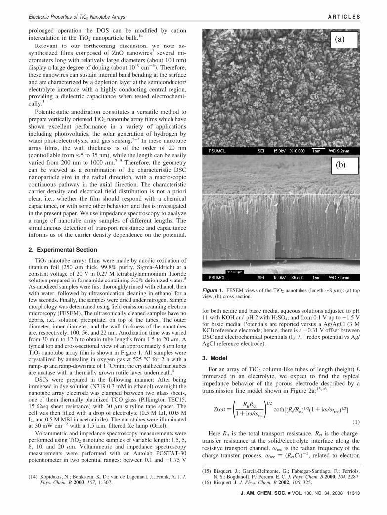
As-anodized samples were first thoroughly rinsed with ethanol, thenwith water, followed by ultrasonication cleaning in ethanol for afew seconds. Finally, the samples were dried under nitrogen. Samplemorphology was determined using field emission scanning electronmicroscopy (FESEM). The ultrasonically cleaned samples have nodebris, i.e., solution precipitate, on top of the tubes. The outerdiameter, inner diameter, and the wall thickness of the nanotubesare, respectively, 100, 56, and 22 nm. Anodization time was variedfrom 30 min to 12 h to obtain tube lengths from 1.5 to 20 µm. Atypical top and cross-sectional view of an approximately 8 µm longTiO2 nanotube array film is shown in Figure 1. All samples werecrystallized by annealing in oxygen gas at 525 °C for 2 h with aramp-up and ramp-down rate of 1 °C/min; the crystallized nanotubesare anatase with a thermally grown rutile layer underneath.4
DSCs were prepared in the following manner: After beingimmersed in dye solution (N719 0.3 mM in ethanol) overnight thenanotube array electrode was clamped between two glass sheets,one of them thermally platinized TCO glass (Pilkington TEC15,15 Ω/sq sheet resistance) with 30 µm suryline tape spacer. Thecell was then filled with a drop of electrolyte (0.5 M LiI, 0.05 MI2, and 0.5 M MBI in acetonitrile). The nanotubes were illuminatedat 30 mW cm-2 with a 1.5 a.m. filtered Xe lamp (Oriel).
Voltammetric and impedance spectroscopy measurements wereperformed using TiO2 nanotube samples of variable length: 1.5, 5,8, 10, and 20 µm. Voltammetric and impedance spectroscopymeasurements were performed with an Autolab PGSTAT-30potentiometer in two potential ranges: between 0.1 and -0.75 V
for both acidic and basic media, aqueous solutions adjusted to pH11 with KOH and pH 2 with H2SO4, and from 0.1 V up to -1.5 Vfor basic media. Potentials are reported versus a Ag/AgCl (3 MKCl) reference electrode; hence, there is a -0.31 V offset betweenDSC and electrochemical potentials (I3
-/I- redox potential vs Ag/AgCl reference electrode).
3. Model
For an array of TiO2 column-like tubes of length (height) Limmersed in an electrolyte, we expect to find the typicalimpedance behavior of the porous electrode described by atransmission line model shown in Figure 2a:15,16
Z(ω)) ( RtrRct
1+ iω/ωrec)1/2
coth[(Rt/Rct)1/2(1+ iω/ωrec)1/2]
(1)
Here Rtr is the total transport resistance, Rct is the charge-transfer resistance at the solid/electrolyte interface along theresistive transport channel. ωrec is the radian frequency of thecharge-transfer process, ωrec ) (RctC3)-1, related to electron
(14) Kopidakis, N.; Benkstein, K. D.; van de Lagemaat, J.; Frank, A. J. J.Phys. Chem. B 2003, 107, 11307.
(15) Bisquert, J.; Garcia-Belmonte, G.; Fabregat-Santiago, F.; Ferriols,N. S.; Bogdanoff, P.; Pereira, E. C. J. Phys. Chem. B 2000, 104, 2287.
(16) Bisquert, J. J. Phys. Chem. B 2002, 106, 325.
Figure 1. FESEM views of the TiO2 nanotubes (length ∼8 µm): (a) topview, (b) cross section.
J. AM. CHEM. SOC. 9 VOL. 130, NO. 34, 2008 11313
Electronic Properties of TiO2 Nanotube Arrays A R T I C L E S

lifetime17 by τn ) ωrec-1. C3 is the total capacitance in the solid
phase and the solid-electrolyte interface. C3 has several possiblecontributions:18 (1) the chemical capacitance of the semiconduc-tor, Cµ, (2) the depletion capacitance in the semiconductorsurface, Cdpl, and (3) the Helmholtz capacitance of the surface,CH. Total film capacitance has an additional contribution fromthe exposed surface of the barrier layer at the bottom of thecolumns, Cback, see Figure 2a.
In the case of low reactivity with respect to electron transport,as given by the condition Rct > Rt,15 for frequencies higher thanω1 ) (RtC3)-1 eq 1 reduces to
Z) (Rtr
C3)1/2
(iω)-1/2 (2)
Equation 2 is often termed the “Warburg” impedance,appearing as a 1-slope line in the complex impedance plot shownin the left of Figure 2b. It should be emphasized that, in contrastto semi-infinite diffusion, in the transmission line model the45° characteristic appears only in the high-frequency part ofthe impedance spectrum. As the frequency decreases (ω < ω1)the charge-transfer resistance gives rise to a semicircle at lowfrequency, consisting of the parallel combination of Rct and C3
as shown in the right of Figure 2b.The nanotube array presents the characteristic behavior of
nanoparticulate TiO2 networks usually found in DSCs2,19,20 withlittle intrinsic doping by foreign atoms and consequently ahomogeneous conduction band level throughout the semicon-ductor. The bias potential V determines the Fermi level position
with respect to the conduction band, whereas the transportresistance in the TiO2 displays the potential dependence2
Rtr )R0tr exp[qVkT ] (3)
with q the elementary positive charge. Rtr is large at lowpotentials due to the absence of free carriers; therefore, nocontribution from the TiO2 nanotubes to capacitance and charge-transfer resistance is expected. In this regime the majority ofthe cell capacitance will come from the exposed barrier layer,with a value of the order of 10 µF · cm-2. The TiO2 capacitanceincreases with applied potential by21
Cµ )C0µ exp[-RqVkT ] (4)
with R < 1, until it reaches the value of the CH given by thetotal surface of the tubes.
4. Results and Discussion
Electrochemical measurement of the nanotube array samplesprovided a variety of behaviors that we analyze on a case bycase basis. First, while keeping the samples in a basic (pH 11)electrolyte medium at moderate applied potentials (<1 V), theypresented the general behavior described by eq 1, shown inFigure 3. The parameter values obtained from impedance (C3,Rtr, Rct) follow quite accurately the trends stated in eqs 3 and 4.The resulting parameters for the 10 µm sample are shown inFigure 4, with a chemical capacitance value of R ) 0.21, charge-transfer resistance coefficient of 0.40, and transport resistanceslope of 84 mV/decade, the values of which are comparable tothose obtained for nanocolloid-based films.2,13,19,20 The clearexperimental observation of transmission line behavior (Figure3) indicates that the capacitance and charge-transport resistanceare due to the electronic response of the TiO2 nanotubes,whereas the impedance behavior can be unambiguously inter-preted in terms of the model of Figure 2a providing informationon the carrier distribution within the tubes. As seen in Figure 4when the applied bias potential was brought to large negativevalues (< -1.5 V) or kept at moderate potentials (≈ -1 V formore than 20 min) in basic media, the impedance resultschanged dramatically. The transport resistance is reduced andmaintains a nearly constant value, indicating a large chargecarrier density insensitive to applied voltage. This is a strongindication of highly doped behavior. In addition, the chemical
(17) Bisquert, J.; Zaban, A.; Greenshtein, M.; Mora-Sero, I. J. Am. Chem.Soc. 2004, 126, 13550.
(18) Bisquert, J. Phys. Chem. Chem. Phys. 2003, 5, 5360.(19) Fabregat-Santiago, F.; Bisquert, J.; Garcia-Belmonte, G.; Boschloo,
G.; Hagfeldt, A. Sol. Energy Mater. Sol. Cells 2005, 87, 117.(20) Bisquert, J. Phys. Chem. Chem. Phys. 2008, 10, 3175.
Figure 2. (a) Transmission line equivalent circuit model applied to theTiO2 nanotube array films. (b) Characteristic impedance response of ananotube electrode. The large arc is the parallel combination of Rct and C3.The left panel shows in expansion the high-frequency 45°-like behaviordue to transport of electrons in the semiconductor. The frequencies ω1 andωrec are defined in the main text.
Figure 3. Impedance spectra of a TiO2 nanotube array film initially heldat -1 V for 20 min, i.e., “aged”, pH 11, showing typical transmission linebehavior with low-frequency recombination arc and high-frequency 45° line.Impedance was performed at -0.7 V.
11314 J. AM. CHEM. SOC. 9 VOL. 130, NO. 34, 2008
A R T I C L E S Fabregat-Santiago et al.

capacity of TiO2 increases enormously, with values ranging from1 to 6 mF · cm-2 at low potentials, reaching close to 80mF · cm-2 at the highest applied potential. These values approachthose of supercapacitors (≈0.3-1 F · cm-2),21 see Figure 4a.Larger values of capacitance are obtained with increasingnanotube length. We attribute the observed modifications underlarge negative bias in basic medium to proton uptake in thenanotube walls, which also changed the clear walls to a bluecolor. Proton uptake in nanocrystalline TiO2 was demonstratedby Hupp and co-workers using a photoelectrochemical quartzcrystal microbalance technique.22,23 Proton intercalation withinthe TiO2 nanotubes results in free electrons that, in turn, decreasethe electrical resistance. The cation intercalation results in amuch larger capacitance, most likely due to formation of adepletion region at the semiconductor surface.24 Figure 5a showscyclic voltammetric measurements of a 10 µm long nanotubesample prior to and after proton intercalation. The capacitivecurrent25 is much higher for the cation-intercalated filmsindicating a great increase in the capacitance at low potentials.Figure 5b shows the dynamic intercalation process in an 8 µmsample.During the first cathodic scan, starting at 0 V, at low negativepotentials the capacity is small, whereas in the return anodic
scan the capacitance is much larger. In the second cathodic scanthe capacitance is large even at low potentials and, with respectto the first scan, further increases in the anodic return.
Measurements were also done in acidic media (pH 2), andin this case high capacitance values were observed in allsamples, see Figure 6a. The transport resistance is so low itcannot be reliably measured. The capacitance increase at thehighest negative potentials appears due to the unpinning of theFermi level that occurs at potentials more negative than -0.8V allowing the Fermi level to approach the conduction band.25
The results indicate that the nanotube array samples are proton-
(21) Winter, M.; Brodd, R. J. Chem. ReV. 2004, 104, 4245.(22) Lemon, B. I.; Hupp, J. T. J. Phys. Chem. 1996, 100, 14578.(23) Yan, S. G.; Hupp, J. T. J. Phys. Chem. 1996, 100, 2667.(24) Munoz, A. G. Electrochim. Acta 2007, 52, 4167.(25) Fabregat-Santiago, F.; Mora-Sero, I.; Garcia-Belmonte, G.; Bisquert,
J. J. Phys. Chem. B 2003, 107, 758.(26) Fabregat-Santiago, F.; Bisquert, J.; Palomares, E.; Otero, L.; Kuang,
D.; Zakeeruddin, S. M.; Gratzel, M. J. Phys. Chem. C 2007, 111, 6550.
Figure 4. Comparison of parameters from impedance data, from theequivalent circuit model of Figure 2a, as a function of electrode potential,for a 10 µm sample before (fresh) and after being held at -1 V for 20 minin basic solution (aged), and in a DSC. (a) Capacitance per unit geometricarea, C3, (b) transport resistance, and (c) charge-transfer resistance. Notethat for comparison DSC values have been shifted -0.31 V (I3
-/I- redoxpotential vs Ag/AgCl reference electrode).
Figure 5. (a) Cyclic voltammetries of a 10 µm sample before (fresh) andafter application of a strong bias potential (aged) while measuringimpedance. (b) The intercalation process during a voltammetry of sufficientpotential in a 8 µm long nanotube array sample.
Figure 6. (a) Capacitance of TiO2 nanotubes, per unit geometric area ofthe film, in basic and acidic media. (b) Same capacitance data rescaled tovolume density, by dividing by nanotube length.
J. AM. CHEM. SOC. 9 VOL. 130, NO. 34, 2008 11315
Electronic Properties of TiO2 Nanotube Arrays A R T I C L E S

intercalated even in the absence of the negative bias that wasrequired in basic media.
Figure 6 enables comparison of the capacitance behavior ofthe nanotube array films as a function of nanotube array lengthin both basic and acid electrolytes. We note the displacementof the capacitance values along the voltage axis, which isexpected by the change of the TiO2 conduction band at differentpH values. The capacitance scales with nanotube length. Thesmall dispersion of the rescaled values in Figure 6b is attributedto minor differences in wall thickness of the different samples.In summary, it is observed that “fresh” nanotube array samplesin basic medium display the standard behavior of crystallineTiO2 nanoparticles, consisting of initially low conductivity andchemical capacitance that exponentially increase with biaspotential.2,19 These properties change dramatically upon negativebias, whereupon the sample displays the behavior characteristicof a highly doped semiconductor, i.e., a high capacitance and alow charge-transport resistance nearly independent of bias. Weattribute this change to the intercalation of protons from waterinto the nanotubes. In acidic media the high proton concentrationof the electrolyte facilitates intercalation, whereas in basicsolution it requires application of a negative potential. Furtherquantitative analysis of the capacitance data to extract thevolume density of carriers requires an extension of theMott-Schottky model in cylindrical coordinates3 to match thetubular geometry and consideration of the frequency effect ofband gap states.24
4.1. Dye Solar Cell Characterization. Back-side-illuminatedDSCs were fabricated using a 10 µm long TiO2 nanotube arrayfilm on a Ti foil substrate. Prior to DSC fabrication the nanotubearray film was held at -1 V for 20 min in acidic solution.Considering our previous discussion, the performance of theelectron-transporting nanotube arrays are expected to be alteredby proton intercalation. From the current density-potential(j-V) curve, Figure 7, we obtain an efficiency of 3.1%, short-circuit current of 3.1 mA cm-2, photopotential 0.63, and fillfactor of 0.44. Although unoptimized, this DSC is significantlyless efficient than previous reports for the same devicegeometry.5–7 The impedance measurements of Figure 4 allowus to identify the central factors determining the relatively poorshape of the j-V curve:26,27
(i) The high capacitance obtained for the DSC, Figure 4a,indicates that the TiO2 nanotubes have been cation-intercalated.This property may limit the movement of the Fermi level inthe semiconductor, thus limiting Voc.
(ii) The recombination resistance, Figure 4c, is comparativelylow19,26 indicating that cation intercalation, or doping, enhancesrecombination. It appears enhanced recombination is responsiblefor the pronounced slope at low potentials in the DSC whichcontributes to a reduction in the fill factor and, additionally,limits Voc.26,27
(iii) TiO2 intercalation, observed through capacitance measure-ments, is confirmed by the nearly constant value obtained forthe transport resistance. The values obtained for Rtr in the DSCsamples are higher than expected. These transport resistancevalues accurately describe the slope of the j-V curve at highnegative potentials, related to a high overall series resistanceand poor fill factor.26,27 The contributions to the overallresistance found for these DSC samples were 20 Ω from theconducting glass and titanium foil, 7 Ω from the Pt counterelectrode, from 20 to 100 Ω (depending on the potential) fromthe diffusion of the redox in the electrolyte, and values above200 Ω () Rtr/316) from electron transport in the TiO2.
From these results we can infer that unintentional doping,i.e., intercalation, may have detrimental effects on DSCperformance due mainly to the pinning of the Fermi level andincrease of recombination. Strategies for improving DSCperformance by electrochemical doping include the formationof fast transport states28 and the formation of core-shell orgraded doping of the metal-oxide including a fast transportchannel.29 Such approaches could decrease the electron-transportresistance to improve the photocurrent while allowing for Fermilevel displacement and consequently a larger photovoltage. Thepossibility of unwanted TiO2 intercalation suggests long-termDSC stability may be enhanced by substitution of the lithiumions by larger ones such as tetrabutylammonium or guanidinium.
5. Conclusions
The carrier density in TiO2 nanotube array films may presentvery different behaviors depending on the electrolyte andelectrochemical treatment. In basic media the films display thestandard behavior of nanoparticulate TiO2 films with a chemicalcapacitance exponentially dependent on the bias potential. Thiscan be modified to demonstrate a very high capacitance, duewe believe to the intercalation of protons into the TiO2, offeringthe possibility for application in supercapacitors. Proton inter-calation, or doping of the nanotubes in acidic media, is readilyachieved, whereas that in basic media requires application ofstrong negative potentials. DSCs prepared with the nanotubespreviously intercalated with protons from solution showedlimited performance. In this case charge transport within thetitanium dioxide was found to be the main contribution tothe DSC series resistance. Our results show that impedancespectroscopy is an effective tool for in situ investigation of theconduction and accumulation properties of advanced metal-oxidearchitectures for enhanced DSC operation.
Acknowledgment. J.B. acknowledges financial support fromMinisterio de Educacion y Ciencia under projects MAT2007-62982and HOPE CSD2007-00007 (Consolider-Ingenio 2010). C.A.G.acknowledges financial support from the Department of Energy DE-FG02-06ER15772.
JA710899Q(27) Sze, S. M. Physics of Semiconductor DeVices, 2nd ed.; John Wiley
and Sons: New York, 1981.(28) Wang, Q.; Zhang, Z.; Zakeeruddin, S. M.; Gratzel, M. J. Phys. Chem.
C 2008, 112, 7084.(29) Chappel, S.; Grinis, L.; Ofir, A.; Zaban, A. J. Phys. Chem. B 2005,
109, 1643.
Figure 7. Current density-potential curve of a DSC made from a 10 µmnanotube film “aged” by being held at -1 V for 20 min.
11316 J. AM. CHEM. SOC. 9 VOL. 130, NO. 34, 2008
A R T I C L E S Fabregat-Santiago et al.