high-capacity chipless rfid tag insensitive to the polarization
TRANSCRIPT
IEEE TRANSACTIONS ON ANTENNAS AND PROPAGATION, VOL. 60, NO. 10, OCTOBER 2012 4509
High-Capacity Chipless RFID Tag Insensitiveto the Polarization
Arnaud Vena, Etienne Perret, Member, IEEE, and Smail Tedjini, Senior Member, IEEE
Abstract—Designing a reader for chipless RFID is a hard tasksince both the polarization and operating frequency agility haveto be implemented. The new tag design proposed in this paper ispolarization independent, making the design of the reader easiersince only linear polarization is needed to detect the tag. The pro-posed chipless tag is based on multiple circular ring patch res-onators. The coding capacity of this tag reaches 19 bits within acompact surface of cm . Further, the frequency band iswithin 3.1 to 10.6 GHz to be compliant with FCC and ECC regula-tions for UWB. This new design is experimentally validated in thefrequency domain using bi-static measurement set-up. Both am-plitude and group delay responses of the tag are investigated andcarried out.
Index Terms—Chipless, frequency shift encoding, group delay,polarization independent, radio-frequency identification (RFID),RCS.
I. INTRODUCTION
R EMOTE identification techniques are an active field ofresearch in which radio-frequency identification (RFID)
technology became one of the intensively investigated majortopic. It consists of using electromagnetic waves to remotelyidentify any object containing a specific tag. A conventionalUHF RFID tag is composed of a silicon chip connected to anantenna. This simple association allows the chip to scavengeenough power and communicate wirelessly with a base station.However, for certain applications, where tag cost and robust-ness are key features, conventional RFID tags exhibit severalpractical drawbacks [1].To overcome these limitations and address new applications,
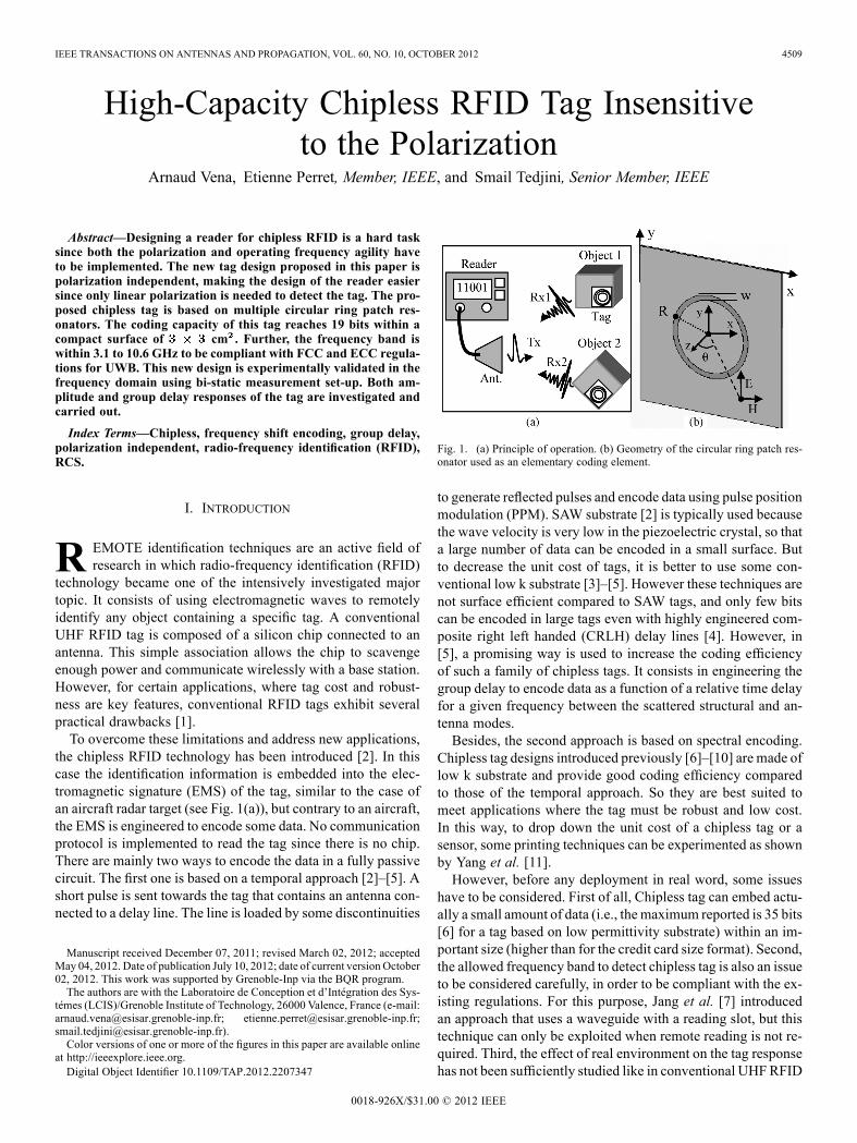
the chipless RFID technology has been introduced [2]. In thiscase the identification information is embedded into the elec-tromagnetic signature (EMS) of the tag, similar to the case ofan aircraft radar target (see Fig. 1(a)), but contrary to an aircraft,the EMS is engineered to encode some data. No communicationprotocol is implemented to read the tag since there is no chip.There are mainly two ways to encode the data in a fully passivecircuit. The first one is based on a temporal approach [2]–[5]. Ashort pulse is sent towards the tag that contains an antenna con-nected to a delay line. The line is loaded by some discontinuities
Manuscript received December 07, 2011; revised March 02, 2012; acceptedMay 04, 2012. Date of publication July 10, 2012; date of current version October02, 2012. This work was supported by Grenoble-Inp via the BQR program.The authors are with the Laboratoire de Conception et d’Intégration des Sys-
témes (LCIS)/Grenoble Institute of Technology, 26000 Valence, France (e-mail:[email protected]; [email protected];[email protected]).Color versions of one or more of the figures in this paper are available online
at http://ieeexplore.ieee.org.Digital Object Identifier 10.1109/TAP.2012.2207347
Fig. 1. (a) Principle of operation. (b) Geometry of the circular ring patch res-onator used as an elementary coding element.
to generate reflected pulses and encode data using pulse positionmodulation (PPM). SAW substrate [2] is typically used becausethe wave velocity is very low in the piezoelectric crystal, so thata large number of data can be encoded in a small surface. Butto decrease the unit cost of tags, it is better to use some con-ventional low k substrate [3]–[5]. However these techniques arenot surface efficient compared to SAW tags, and only few bitscan be encoded in large tags even with highly engineered com-posite right left handed (CRLH) delay lines [4]. However, in[5], a promising way is used to increase the coding efficiencyof such a family of chipless tags. It consists in engineering thegroup delay to encode data as a function of a relative time delayfor a given frequency between the scattered structural and an-tenna modes.Besides, the second approach is based on spectral encoding.
Chipless tag designs introduced previously [6]–[10] are made oflow k substrate and provide good coding efficiency comparedto those of the temporal approach. So they are best suited tomeet applications where the tag must be robust and low cost.In this way, to drop down the unit cost of a chipless tag or asensor, some printing techniques can be experimented as shownby Yang et al. [11].However, before any deployment in real word, some issues
have to be considered. First of all, Chipless tag can embed actu-ally a small amount of data (i.e., the maximum reported is 35 bits[6] for a tag based on low permittivity substrate) within an im-portant size (higher than for the credit card size format). Second,the allowed frequency band to detect chipless tag is also an issueto be considered carefully, in order to be compliant with the ex-isting regulations. For this purpose, Jang et al. [7] introducedan approach that uses a waveguide with a reading slot, but thistechnique can only be exploited when remote reading is not re-quired. Third, the effect of real environment on the tag responsehas not been sufficiently studied like in conventional UHFRFID
0018-926X/$31.00 © 2012 IEEE
4510 IEEE TRANSACTIONS ON ANTENNAS AND PROPAGATION, VOL. 60, NO. 10, OCTOBER 2012
tags [12]. Fourth, the chipless technology is intrinsically notsuitable for reading multiple tags at a time although some tech-niques based on spatial and temporal separations, have been in-troduced by Hartmann et al. [13]. Last, but not least, the reli-ability of the reading system such as the possible detection ir-respective of the polarization of the electromagnetic wave wasalso not considered. In most of the previous designs, the polar-ization issue is relevant, both for configuration using multiplescatterers [7]–[10], and for design using two cross-polarized an-tennas connected to a filtering circuit [6]. As a result, to detectthe tag regardless of its orientation, the reader needs to imple-ment polarization agility, making the design more complex interms of signal processing and antenna feeding. Moreover, thecalibration task becomes more complex if more than one linearpolarization is used, because the detection environment has tobe well known for each polarization.The proposed design brings a real improvement in terms of
detection reliability since it consists of an EMS totally indepen-dent of the polarization of the incident wave. Basically, the de-sign is made of multiple circular ring patch resonators. They arenested to decrease the overall size of the tag and provide a betterdensity of coding per surface than for [7] which employs splitrings resonators arranged side by side.To increase the detection reliability, the measurement of the
amplitude can be combined to the group delay measurement.Indeed since resonances exhibit a high quality factor one canobserve sharp phase transitionmaking large group delay for spe-cific frequencies.
II. CIRCULAR RING PATCH BEHAVIOR
Themain objective/goal of this of new technology is to designchipless tags having an EM response as constant as possibleirrespective of the polarization of the incident wave in order toimprove the practical implementation. The circular ring patchshown in Fig. 1(b) seems to be the best candidate to realize thisneed. This is a well-known structure [14]. It physically exhibitssymmetry around its center. Since it is not filled by any materialinside the annulus, the space can be used to put an additional ringof smaller size. This nesting technique has already been used in[15]. However, in this alternative work, the circular rings areopened as for a split ring resonator. The aim of this work was,to increase coding efficiency taking advantage from polarizationdiversity, and making it possible to sense the rotation angle ofan object at the expense of a more complex reading system.Besides, contrary to [16] which also uses circular rings
etched on one or two layers, the chipless tag presented here hasa ground plane. So it is robust to the material influence of theobject to identify. Moreover, in [16] there is no engineeringof the shape to accurately control the location of peaks inthe frequency spectrum response. Instead, they are generatedrandomly to create random responses. This implies the use of adatabase to store all the identifiers. To recover the identifier, theEM signature of a specific tag is compared to the tag database.
A. The Way of Radiation
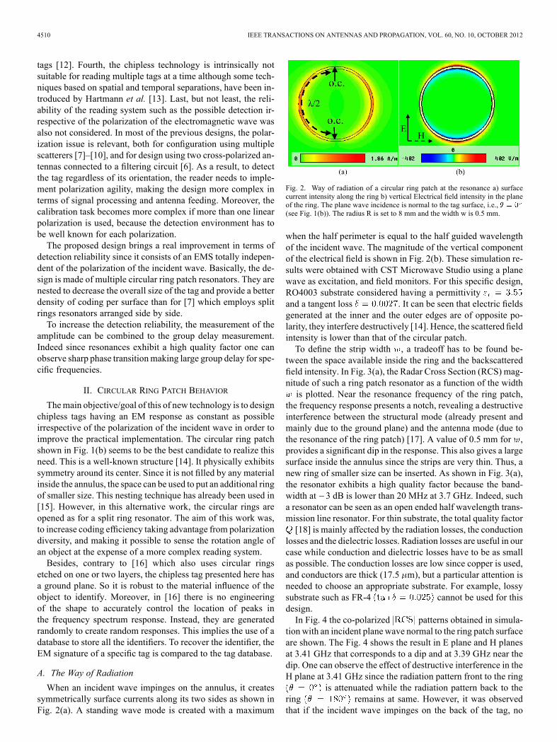
When an incident wave impinges on the annulus, it createssymmetrically surface currents along its two sides as shown inFig. 2(a). A standing wave mode is created with a maximum
Fig. 2. Way of radiation of a circular ring patch at the resonance a) surfacecurrent intensity along the ring b) vertical Electrical field intensity in the planeof the ring. The plane wave incidence is normal to the tag surface, i.e.,(see Fig. 1(b)). The radius R is set to 8 mm and the width w is 0.5 mm.
when the half perimeter is equal to the half guided wavelengthof the incident wave. The magnitude of the vertical componentof the electrical field is shown in Fig. 2(b). These simulation re-sults were obtained with CST Microwave Studio using a planewave as excitation, and field monitors. For this specific design,RO4003 substrate considered having a permittivityand a tangent loss . It can be seen that electric fieldsgenerated at the inner and the outer edges are of opposite po-larity, they interfere destructively [14]. Hence, the scattered fieldintensity is lower than that of the circular patch.To define the strip width , a tradeoff has to be found be-
tween the space available inside the ring and the backscatteredfield intensity. In Fig. 3(a), the Radar Cross Section (RCS) mag-nitude of such a ring patch resonator as a function of the widthis plotted. Near the resonance frequency of the ring patch,
the frequency response presents a notch, revealing a destructiveinterference between the structural mode (already present andmainly due to the ground plane) and the antenna mode (due tothe resonance of the ring patch) [17]. A value of 0.5 mm for ,provides a significant dip in the response. This also gives a largesurface inside the annulus since the strips are very thin. Thus, anew ring of smaller size can be inserted. As shown in Fig. 3(a),the resonator exhibits a high quality factor because the band-width at 3 dB is lower than 20 MHz at 3.7 GHz. Indeed, sucha resonator can be seen as an open ended half wavelength trans-mission line resonator. For thin substrate, the total quality factor[18] is mainly affected by the radiation losses, the conduction
losses and the dielectric losses. Radiation losses are useful in ourcase while conduction and dielectric losses have to be as smallas possible. The conduction losses are low since copper is used,and conductors are thick (17.5 m), but a particular attention isneeded to choose an appropriate substrate. For example, lossysubstrate such as FR-4 cannot be used for thisdesign.In Fig. 4 the co-polarized patterns obtained in simula-
tion with an incident plane wave normal to the ring patch surfaceare shown. The Fig. 4 shows the result in E plane and H planesat 3.41 GHz that corresponds to a dip and at 3.39 GHz near thedip. One can observe the effect of destructive interference in theH plane at 3.41 GHz since the radiation pattern front to the ring
is attenuated while the radiation pattern back to thering remains at same. However, it was observedthat if the incident wave impinges on the back of the tag, no

VENA et al.: HIGH-CAPACITY CHIPLESS RFID TAG INSENSITIVE TO THE POLARIZATION 4511
Fig. 3. Simulated response versus the width w of the ring. The meanradius R is equal to 8 mm in each case. These results have been obtained withCSTMicrowave Studio using a plane wave as for excitation and a RCS far-fieldprobe front to the tag.
Fig. 4. Simulated co-polarized pattern at 3.39 GHz and 3.41 GHz.(a) E plane. (b) H plane. The plane wave incidence is normal to the tag surface,i.e., (see Fig. 1(b)). The radius R is set to 8.5 mm and the width w is0.5 mm.
significant dip in the frequency signature is visible. Another in-teresting feature of this resonator concerns its phase. Since thequality factor is important; the phase changes are very rapid.Consequently, the group delay can be important, i.e., equal to12 ns for mm (see Fig. 3(b)). Moreover, increasing
the width to 2 mm allows getting a value close to 50 ns.Group delay parameter should be preferable, especially in thecase of a noisy environment.Equation (1) can be used to calculate analytically the reso-
nance frequency of this notch. It is derived from the transmis-sion line model [18]. The parameter is the radius of the ringand is the effective permittivity calculated for a microstrip
Fig. 5. (a) Photography of the chipless tag made of three nested circular ringpatches. , and are the mean radii of respectively ring 1 to 3. It isassumed that the y axis is aligned with the normal to the tag’s surface when
. (b) Design based on 12 nested circular rings aligned side by side.
line of width , height , and permittivity . Since there arefringing fields up and down the circle, the electrical length islittle bit larger than the calculated guided half wavelength. So,the multiplication of the radius R by a correcting factor, (foundexperimentally) in (1) is needed to get a good approximation ofthe resonance frequency. This equation is valid for a radiusbetween 9 and 4 mm and for a width mm:
(1)
B. Nested Circular Ring Patches
The circular ring patch exhibits a high quality factor and ispolarization independent. So, it is a good candidate to be theelementary scatterer of a chipless tag. The design shown inFig. 5(a) is composed of three nested circular ring patches. Thefrequency bandwidth has been chosen to be compatible with theultrawide band (UWB) between 3.1 and 10.6 GHz. So the firstresonator denoted 1 can vary between 3.1 and 5.6 GHz, whilethe second one can vary between 5.6 and 8.1 and the last onebetween 8.1 and 10.6 GHz.To limit the coupling between each circular ring, a minimum
gap separation has to be respected, but this is problematic sincein this way the frequency span of the two first rings is reduced.So it is preferable to take into account these coupling effects inthe model in order to compensate it. However, if rings are tooclose from each other, the inner one cannot radiate as well.To do further size reduction, the nesting technique can be
combined to the multiplication of rings side by side. With thistechnique a tag having 12 resonators within a size of cmcan be realized (see Fig. 5(b)). The 12 rings operate in the fullUWB band and the frequency span available for each resonatoris equal to 625 MHz.
C. Final Design and Coding Technique
The coding technique used is frequency shift encoding (seeFig. 6) already applied in some previous work [9]. This tech-nique allows an increase in terms of coding efficiency so thatmore than one bit can be encoded for each resonator. In the ex-ample of Fig. 6, three rings resonators are used and each res-onance frequency (dip) can vary between four values. Thus, 2bits can be encoded for each ring resonator. In reality it depends

4512 IEEE TRANSACTIONS ON ANTENNAS AND PROPAGATION, VOL. 60, NO. 10, OCTOBER 2012
Fig. 6. Frequency shift encoding technique applied to the current design.
TABLE IDIMENSIONS OF CHIPLESS TAG BASED ON THREE RESONATORS mm
on the allowed bandwidth for each resonator so that more than 4values are possible. An ID is made by the association of “digit”, , and of base 4. To make the link between the fre-
quency shift of a resonance dip relative to its initial frequencyand its associated digit , (2) can be used. The frequency
resolution is determined by the selectivity of the resonance.So, a patch resonator is well suited for this application since ithas a high quality factor:
(2)
For this design, an estimation of the number of coding slotsis done. We have 7.5 GHz of total bandwidth (from 3.1 to10.6 GHz) and a resolution frequency quite equal to 30 MHz.So we get 250 coding slots to share between three circularring resonators for the first design (see Fig. 5(a)). Thus, eachresonator has 80 coding slots and three isolation slots (i.e.,100 MHz). Hence, the number of combinations can be esti-mated to , i.e., 19 bits. For the 12 resonators tagversion shown in Fig. 5(b), theoretically, each resonator couldhave 17 coding slots and three isolation slots making a codingcapacity as high as 49 bits.
III. VALIDATION AND WAY OF DETECTION
To validate the design, four tags, denoted Tag 1 to 4, havingthree nested resonators with various ring radii and a tag denotedTag 5 with 12 resonators have been realized. The width of stripis mm for all the rings and the thickness of the substrateis 0.5 mm. In Table I, the radius values for each tag are gathered.To measure the EMS in the frequency domain, a bi-static mea-surement setup is used as shown in Fig. 7(a). It is composed ofa vector network analyzer (VNA) Agilent 8722D with a band-width of 20 GHz. Both VNA ports are connected to ridged hornantennas having a gain of 12 dBi in the band 0.7 to 18 GHz. Thetag under test is located at 40 cm from the antennas, which arealso separated by 40 cm. Since there exists a strong couplingbetween antennas, a calibration technique is used to remove
Fig. 7. (a) Measurement Setup. (b) View of the chipless tag put on a cardboardfilled with paper sheets.
these static unwanted effects. Moreover, antennas and cables re-sponses have to be compensated to provide an accurate result.To do so, an initial measurement is done without any tag. Then,a second measurement is done with a reference target having aknown RCS. Finally, the measurement with the tag is done. Thefollowing formula (3) derived from [19] is used to recover thevalue of the complex RCS of the tag :
(3)
The phase of EMS can be used to calculate the group delayof the tag. Unlike the amplitude, for given reading range, itsvariations are not affected by the tag location. If looking tothe measured amplitude response (see Fig. 8(a) and Fig. 8(c)),variations between 2 and 3 dB are visible, so it is hard todetect them with a reading system. However, as shown inFigs. 8(b), (d), (e), and (f), the measured group delays showgreat deviations for all the resonances. One can notice that aresonance dip produces a group delay between 4 and 7 ns(see Figs. 8(d), (e) and (f)), while for other frequencies theambient noise produces a value higher than 2 ns. So a detec-tion system can simply take into account the resonances fromwhich the group delay is below than 2 ns. This measurementalso confirms the very narrow bandwidth of the resonance dip.Thus, for encoding, a frequency resolution lower than 30 MHzcan be considered as reasonable and adopted.In Table II, the measured resonance frequencies of several
tags are shown. To compare, the values obtained using (1) andby a full 3D simulation are given. One can observe a very goodagreement between measurements, simulations and analyticalmodels.In terms of coding, the independence of each ring resonator
is confirmed by measurements, so that an independent ID canbe assigned for each ring. The resonance frequencies of the tag1 are taken as the reference, so according to (2), the associ-ated code is 0.0.0. From tag 1 to tag 2, only the frequencyrises from 3.39 to 3.44 GHz, so we can assign the code 1.0.0 tothe tag 2. In a same way we can find that tag 3 encode 2.1.1and tag 4, 3.2.2. This validates the concept of the frequencyshift encoding technique. Although in this case, for sake of sim-plicity the frequency resolution is not chosen to be constant.To validate the detection reliability of this design, the tag wasput on a cardboard filled with paper sheets (see Fig. 8(b)) andFig. 9(a) and (b) shows the results obtained. One can noticethat these results are quite similar to the previous one (those ob-tained for free space case), and the obtained group delay values

VENA et al.: HIGH-CAPACITY CHIPLESS RFID TAG INSENSITIVE TO THE POLARIZATION 4513
Fig. 8. Measurements results for tags 1 to 4 using the bi-static measurement set-up of Fig. 8(a) for free space case (b) Group delay for free space case(c) Zoom of result in free space around the resonant frequency of ring 1. (d) Zoom of the group delay in free space around the resonant frequency of thecircular ring 1. (e) Zoom of the group delay in free space around the resonant frequency of the circular ring 2. (f) Zoom of the group delay in free space around theresonant frequency of the circular ring 3.
TABLE IIMEASURED RESONANCE FREQUENCY FOR SEVERAL CONFIGURATIONS
AND ASSOCIATED CODE Ci
allow the tag identifier to be decoded without any error. Due tothe presence of a ground plane, no significant frequency shiftwas observed so that a frequency resolution of 30 MHz is stillachievable.Also to confirm the possibility to implement more than three
resonators-based circular ring patches, measurement of the taghaving 12 resonators put on the same filled cardboard was done(see Fig. 10). One can notice that all the 12 resonances can beidentified using both the amplitude and the group delay. Thismakes this structure very suitable for applications that requirea large amount of combinations (more than 40 bits from 3 to9 GHz).
Fig. 9. Measured (a) and (b) group delay for tags 1 to 4 put on a card-board filled with paper sheets.

4514 IEEE TRANSACTIONS ON ANTENNAS AND PROPAGATION, VOL. 60, NO. 10, OCTOBER 2012
Fig. 10. Measured (a) and (b) group delay for chipless tag-based 12 cir-cular ring resonators (see Fig. 6(b)) put on a cardboard filled with paper sheets.
It was observed in simulation and confirmed by measurementthat the tag is still detectable with an incident angle as largeas 90 (see Fig. 1(b)). Consequently a reading system canidentify the tag in the entire halfspace front of the tag. Last,but not least, the polarization independence inherent to the tagwith three resonators is also confirmed both in simulation andmeasurement for the structure having 12 resonators. As a con-sequence, the coupling effect between the ring resonators is alsoindependent of the polarization.
IV. CONCLUSION
This new design based on nested circular ring patch res-onators provides several improvements in terms of detectionand reliability. First, it was demonstrated that the tag is totallyindependent from the wave’s polarization. In addition, resonantdips are still visible for an incident angle as large as the interval
to . This is a key improvement in the field of identi-fication technology, which makes the possible detection of sucha chipless tag even if it is roughly positioned on the item toidentify. Moreover, the use of group delay allows a high degreeof confidence in measurement since it can easily observe therough phase changes at the resonance frequency of rings. Onthe other hand, for both prototypes (3 and 12 resonators), themeasurements made upon a cardboard filled with paper sheetsconfirm the possibility to identify a “lossy” item having a largesize compared to the tag.A capacity of coding of 19 bits is possible using only 3 cir-
cular rings within a size of cm i.e., 2.1 bits/cm . Thisgives one of the best densities of coding per surface (in [8],0.81 bits/cm is attained and in [9] 3.3 bits/cm is reported).This was made possible by using the Frequency Shift Encodingway. A closed form analytical model validated by measure-ments was established. It allows making a link between the ra-dius parameters and a specific code. To increase the coding ca-pacity it was shown that using 12 rings, arranged side by side,it is possible to encode more than 40 bits within cm .
Since the resonators are designed to operate between 3.1 and10.6 GHz, they are compatible with the FCC rules for the UWBcommunication systems. A previous work has shown the pos-sibility to detect a chipless tag using a time-domain radar ap-proach [9]. This is a promising way that makes possible to detectthe tag at a read range of 1 m while respecting the power maskspecified by the FCC. Future developments will contribute tosimplify the calibration technique to make the reading systemmore robust to environment in particular the tag location.
ACKNOWLEDGMENT
The authors would like to thank R. Nair for her advice to apart of this paper.
REFERENCES
[1] IDTechEx, Printed and Chipless RFID Forecasts, Technologies &Players 2009–2019, [Online]. Available: www.IdtechEx.com
[2] C. S. Hartmann, “A global SAW ID Tag with Large data capacity,” inProc. IEEE Ultrasonics Symp., 2002, pp. 65–69.
[3] L. Zheng, S. Rodriguez, L. Zhang, B. Shao, and L.-R. Zheng, “De-sign and implementation of a fully reconfigurable chipless RFID tagusing Inkjet printing technology,” in Proc. IEEE Int. Symp. CircuitsSyst. ISCAS, 2008, pp. 1524–1527.
[4] C. Mandel, M. Schüßler, M. Maasch, and R. Jakoby, “A novel passivephase modulator based on LH delay lines for chipless microwave RFIDapplications,” in Proc. IMWS, Croatia, 2009.
[5] R. Nair, E. Perret, and S. Tedjini, “Temporal multi-frequency encodingtechnique for chipless RFID applications,” presented at the IEEE Int.Microwave Symp., Montreal, QC, Canada, Jun. 17–22, 2012.
[6] S. Preradovic and N. Karmakar, “Design of fully printable planar chip-less RFID transponder with 35-bit data capacity,” in Proc. 39th Eur.Microw. Week, Rome, Italy, Sep. 2009.
[7] H.-S. Jang, W.-G. Lim, K.-S. Oh, S.-M. Moon, and J.-W. Yu, “Designof low-cost chipless system using printable chipless tag with electro-magnetic code,” Proc. IEEE Microw. Wireless Compon. Lett., vol. 20,no. 11, pp. 640–642, Nov. 2010.
[8] I. Jalaly and D. Robertson, “RF barcodes using multiple frequencybands,” in IEEE MTT-S Dig., Jun. 2005.
[9] A. Vena, E. Perret, and S. Tedjini, “Novel compact RFID chipless tag,”in Proc. PIERS, Marrakesh, Morocco, March 20–23, 2011.
[10] J. McVay, A. Hoorfar, and N. Engheta, “Space-filling curve RFIDtags,” in Proc. IEEE Radio and Wireless Symp., San Diego, CA, pp.17–19.
[11] L. Yang, R. Zhang, D. Staiculescu, C. P. Wong, and M. M. Tentzeris,“A novel conformal RFID-enabled module utilizing inkjet-printed an-tennas and carbon nanotubes for Gas-Detection Applications,” IEEEAntennas Wireless Propag. Lett., vol. 8, pp. 653–656, 2009.
[12] H. Chaabane, E. Perret, and S. Tedjini, “A methodology for the designof frequency and environment robust UHF RFID tags,” IEEE Trans.Antennas Propag., vol. 59, no. 9, pp. 3436–3441, Sep. 2011.
[13] C. Hartmann, P. Hartmann, P. Brown, J. Bellamy, L. Claiborne, andW.Bonne, “Anti-collision methods for global SAWRFID tag systems,” inProc. IEEE Ultrason. Symp., 2004, pp. 805–808.
[14] W. C. Chew, “A broad-band annular-ring microstrip antenna,” IEEETrans. Antenna Propag., vol. AP-30, no. 5, pp. 918–922, Sep. 1982.
[15] A. Vena, E. Perret, and S. Tedjini, “A compact chipless RFID tag usingpolarization diversity for encoding and sensing,” in Proc. IEEE Int.Conf. RFID, Orlando, FL, Apr. 3–5, 2012, pp. 191–197.
[16] K. Yung, C. Chan, and D. Cheng, “Chipless microwave identificationtag,” U.S. patent US2009/0267739, Oct. 2009.
[17] N. C. Karmakar, Handbook of Smart Antennas for RFID System.New York: Wiley-Interscience, 2010, p. 423.
[18] R. Hopkins and C. Free, “Equivalent circuit for the microstrip ring res-onator suitable for broadband materials characterization,” IET Microw.Antennas Propag., vol. 2, no. 1, pp. 66–73, Feb. 2008.
[19] W. Wiesbeck and D. Kähny, “Single reference, three target calibrationand error correction for monostatic, polarimetric free space measure-ments,” Proc. IEEE, vol. 79, no. 10, pp. 1551–1558, Oct. 1991.
VENA et al.: HIGH-CAPACITY CHIPLESS RFID TAG INSENSITIVE TO THE POLARIZATION 4515
Arnaud Vena received the Eng. Dipl. degreein electrical engineering from the Institut Na-tional Polytechnique de Grenoble (Grenoble-INP),Grenoble, France, in 2005, where he is currentlyworking toward the Ph.D. degree.From 2005 to 2009, he worked as an R&D Engi-
neer at ACS Solution France SAS. He was in chargeof development of RFID contactless card readers andcontributed to evolution of the ISO/IEC 14443 regu-lation. In October 2009, he started his research withthe Grenoble Institute of Technology, mainly focused
on design of chipless RFID systems.
Etienne Perret (M’05) was born in Albertville,Savoie, France, on October 30, 1979. He receivedthe Eng. Dipl. degree in electrical engineering fromthe Ecole Nationale Supérieure d’Electronique,d’Electrotechnique, d’Informatique, d’Hydrauliqueet des Télécommunications, Toulouse, France, in2002, and the M.Sc. and Ph.D. degrees from theToulouse Institute of Technology in 2002 and 2005,respectively, all in electrical engineering.From 2005 to 2006, he held a postdoctoral posi-
tion at the Institute of Fundamental Electronics (IEF),Orsay, France. His research activities cover the electromagnetic modeling ofpassive devices for millimeter and submillimeter-wave applications. His cur-rent research interests are in the field of wireless communications, especiallyradio-frequency identification (RFID) with the design and development of an-tennas for RFID tags. Since September 2006, he has been an Assistant Pro-fessor of electronics at the Grenoble Institute of Technology. He has authoredand coauthored more than 50 technical conferences, letters and journal papers,and one book chapter.Dr. Perret is a Technical Program Committee member of IEEE-RFID. He
was keynote speaker and the Chairman of the 11th Mediterranean Microwave
SymposiumMMS’2011. He also served as the Co-Chair of the 29th PIERS 2011in Marrakesh, Morocco.
Smail Tedjini (SM’92) received the Doctor inphysics degree from Grenoble University, Grenoble,France, in 1985.He was an Assistant Professor from 1981 to 1986,
and Senior Researcher for the CNRS from 1986 to1993. He became University Professor in 1993 andsince 1996 he has been a Professor at the ESISARDepartment, Institut National Polytechnique deGrenoble (Grenoble-INP), Grenoble, France. Hisspecialization topics concern electromagnetism, RF,wireless and optoelectronics. He serves as coordi-
nator and staff member in numerous academic programs both for educationand research. In 2006 to 2007, he served as the Director of ESISAR, EmbeddedSystems Department, Grenoble-INP. He has been involved in academicresearch supervision since 1982. He is the Founder and past Director of theLCIS Lab. Now, he is the ORSYS Group Leader. His main topics in researchare applied electromagnetism, modeling of devices, and circuits at both RFand optoelectronic domains. Current research concerns wireless systems withspecific attention to RFID and nanoRF. He supervised 27 Ph.D. candidates andhe has more than 250 publications.Dr. Tedjini is a member of several TPC and serves as expert/reviewer for na-
tional and international scientific committees and conferences including ISO,Piers, IEEE, URSI, ISO, ANR, OSEO, FNQRT, etc. He organized several con-ferences/workshops. He is President and founder of the IEEE-CPMT FrenchChapter, Vice-President of IEEE Section France and elected as the Vice-Chairof URSI Commission D “Electronics and Photonics” in 2008. He was reelectedas Vice-Chair of the IEEE-France section and will serve as the Chair of URSICommission “D3” for the triennium 2011–2014.