hf-ssb automatic antenna tuner - · pdf filei antenna tuning unit ac500 ts5.210 hf-ssb...
TRANSCRIPT
Antenna Tuning Unit AC500 TS5.210
HF-SSB Automatic Antenna Tuner 1.6-30 MHz, 500 W
Owner’s Manual
photograph TBD


Antenna Tuning Unit AC500 TS5.210
HF-SSB Automatic Antenna Tuner 1.6-30 MHz, 500 W
Owner’s Manual


i
Antenna Tuning Unit AC500 TS5.210
HF-SSB Automatic Antenna Tuner 1.6-30 MHz, 500 W
TABLE OF CONTENTS
Para. Page
Performance Specification ..........................................................................................................................................iii
Model Complements .................................................................................................................................................... v
Accessories................................................................................................................................................................... v
CHAPTER 1 DESCRIPTION
1.1 GENERAL DESCRIPTION..................................................................................................................1-1 1.2 FUNCTIONAL AND STRUCTURAL DESCRIPTION ..................................................................1-1
CHAPTER 2 INSTALLATION
2.1 GENERAL ...............................................................................................................................................2-1 2.2 RECOMMENDED EQUIPMENT .......................................................................................................2-1
2.2.1 Tools ...........................................................................................................................................2-1 2.2.2 Accessories .................................................................................................................................2-1
2.3 INSTALLATION INSTRUCTIONS ...................................................................................................2-1 2.3.1 Cable Kits ...................................................................................................................................2-1 2.3.2 Installation Instructions ..............................................................................................................2-1 2.3.3 Operational Check ......................................................................................................................2-4

ii
TABLE OF CONTENTS (Cont.)
Para. Page
CHAPTER 3 THEORY OF OPERATION
3.1 FUNCTIONAL DESCRIPTION.......................................................................................................... 3-1 3.1.1 ATU Function ............................................................................................................................ 3-1 3.1.2 ATU Operation .......................................................................................................................... 3-2
3.2 ELECTRICAL DIAGRAMS DESCRIPTION................................................................................... 3-2 3.2.1 Tuning Sensors Board TS5.281 ................................................................................................. 3-2 3.2.2 Matched Loop Board TS5.282................................................................................................... 3-4 3.2.3 Control Board TS5.283 .............................................................................................................. 3-6
APPENDIX A DIAGRAMS

iii
PERFORMANCE SPECIFICATIONS
ELECTRICAL
Frequency Range 1.6-30 MHz Input Power Capability Not more than 500 W Input Impedance with matched ATU 50 Ω with VSWR not higher than 1.4 Tuning Time Programmed: not higher than 5 seconds
From pre-saved frequencies in memory: not higher than 300 msec RF Tuning Power 3-14 W Antennas For frequency range 1.6-30 MHz:
- 19.46 ft (6 m) to 32.43 ft (10 m) whips - 22.7 ft (7 m) to 97.3 ft (30 m) wire antennas For frequency range 2-30 MHz: - 13 ft (4m) whip
Power Requirements 24 V dc nominal, 2 A

iv
GENERAL
Environmental Conditions
Vibration MIL-STD-810D Method 514.3 and EIA RS152B
Shock MIL-STD-810D Method 516.3 and EIA RS152B
Sand & Dust MIL-STD-810D Method 510.2
Rain MIL-STD-810D Method 506.2
Salt Fog MIL-STD-810D Method 509.2
Operating Temperature -30ºC to +60ºC
Storage Temperature -40ºC to +85ºC
Humidity 95% @ 20ºC to 85ºC
Dimensions (H x W x L) TBD" x TBD" x TBD" (? cm x ? cm x ? cm)
Weight TBD lbs (TBD kg)
Specifications subject to change without notice

v
MODEL COMPLEMENTS
Model TBD
TBD Mobile Automatic Antenna Tuner (ATU-AC500) 500 W
TBD Housing
TBD Antenna Tuner Board
TBD ATU Assembly
TBD RF Coax Cable Kit
TBD ATU AC500, HF-SSB Automatic Antenna Tuner Owner’s Manual
ACCESSORIES TBD RF Cable kit, TBD feet (N Type - UHF)
TBD RF Cable Kit, TBD feet (N Type - UHF)
v/(vi Blank)


1-1
CHAPTER 1
DESCRIPTION
1.1 GENERAL DESCRIPTION
The Mobat HF-SSB Automatic Antenna Tuner Unit (ATU) model AC500 is an antenna matching network that provides efficient RF power transfer from the radio system to the antenna.
The ATU handles up to 500 watts Peak Envelope Power (PEP). It is used for voice and Continuous Wave (CW) Morse code communications.
The ATU AC500 matches the antenna impedance to the 50 Ω output impedance of the radio system, with a nominal VSWR of not higher than 1.4 in the 1.6 to 30 MHz frequency range.
The ATU is housed in a weatherproof aluminum case with four M8 bolts, allowing outdoor installation, such as open roofs. An antenna isolator is located at the top of the case to isolate the antenna input connection made of copper strip (see Figure 1-1). Two bolts with M6 nuts secure the case to ground.
1.2 FUNCTIONAL AND
STRUCTURAL DESCRIPTION
The AC500 Automatic Antenna Tuner (ATU) operates in the 1.6 to 30 MHz frequency range at 500 watts peak envelope power (PEP). The ATU automatically selects the network component for the antenna matching, thus eliminating the need for programming, presetting, manual tuning and adjustment during the installation and the operations.
A control circuit checks the antenna matching, each time the channel is changed, and then automatically switches inductors and capacitors in and out of the matching network. The tuning data for a given channel is stored in a memory and kept as long as the ATU is on. The next time the channel is used, the stored tuning data for that channel is used, considerably reducing the tuning time (provided that the VSWR is within the specified limits).
The AC500 TS5.210 unit comprises the following components (Figure 1-1):
• High Voltage Isolator
• High Voltage Inductor - TS5.210.820
• Chassis with High Voltage Vacuum Relays-
TS5.210.001
• Matched Loop Board - TS5.282
• Sensors Board - TS5.281
• Control Board - TS5.283
• RF and Control Input connectors.

Description
1-2
TBD
a. General View
TBD
b. Structural View
Figure 1-1. AC500 Views

2-1
CHAPTER 2
INSTALLATION
2.1 GENERAL The MICOM Radio and AC500 ATU are factory-preset for proper tuning operation and require no additional adjustment or programming.
2.2 RECOMMENDED EQUIPMENT
2.2.1 TOOLS - Nut driver TBD
- Nut driver TBD
- Flat blade screwdriver TBD
- TBD
2.2.2 ACCESSORIES For base station installations:
TBD High voltage cable kit (supplied with the ATU)
TBD TBD ft cable kit TBD TBD ft cable kit
2.3 INSTALLATION INSTRUCTIONS
2.3.1 CABLE KITS The ATU basic model is supplied with the TBD-Model No. High Voltage Cable Kit and the TBD-Model No. RF coax cable kit.
2.3.2 INSTALLATION INSTRUCTIONS The antenna and the ATU locations on a base station are the most critical parts of radio components installation, since they have a great influence on the effective radiated power.
The installation instructions refer to:
- Antenna Installation
- ATU Installation.
The interconnection between AC500, amplifier PA-500 and MICOM Radio are illustrated in Figure 2-1.

2-2
ChChangeTUNEOKOVER
GND
+24VDC
GND
INPUT RF J1
ANTENNAJ12
ATUTS5. 210
CONTROL J2
MICOM-RADIO
AMPLIFERS500 Watt
12345678910
2233
44
ANTENNA
Figure 2-1. AC500, PA-500 and MICOM Radio Interconnection
2.3.2.1 Antenna Installation
The unit AC500 TS5.210 is intended to provide transmitter’s operation with the following antennas:
- Whip antenna height Н=4m (frequency range 2.0-30.0 MHz)
- Whip antenna height Н=6m-10m (frequency range 1.6-30.0 МHz)
- Wire antennas 7-30 m long.
2.3.2.1.1 Whip antennas
Whip antennas (See Figure 2-2) are connected using an isolated connection protected by a high-voltage insulator. The insulator is designed to work with high voltages not less than 10 kV.
Whip antennas are mounted on top of a building or a base station. The antenna should be located away from interfering structures, such as other antennas, metal masts, buildings and metal wires parallel to the antenna. The radius from these interfering structures to the AC500 antenna should be about 6-10 m. If the antenna is installed on top of a building with a non-metallic roof, the antenna copper wires (with section area 5-6 sq. mm - AWG-TBD) are to be laid radially
around the antenna’s location. The number of copper wires used is not less than 6.
TBD
Figure 2-2. Whip Antenna - Base Station Location
2.3.2.1.2 Wire antennas
The wire antennas (see Figure 2-3), including L-type or T-type, are made of copper cables/ropes with section area not less than 15 sq. mm - AWG-TBD. The number of wires (“beams”) may vary from 1 to 3. The lower point of the wire antenna is mounted on an insulated mounting, to avoid any mechanical loads on the antenna insulator.
Insulators of wire antennas and insulated antenna mountings should work with high voltages not less than 10 kV.

Installation
2-3
When the antenna is installed at ground surface or on top of a building with a non-metallic roof, it is required to lay copper wires (with section area 5-6 sq. mm - AWG-TBD) at all area of projection below the antenna. The number of wires that are connected radially from the antenna’s ends, should be not less than 6, and the number of wires connected perpendicularly below the antenna, should be not less than 1 wire per 2 meters. The length of every wire should be not less than the height of antenna’s mast. The insulation resistance of an antenna-feeder section should be not less than 20 MΩ at normal conditions and not less than 1 MΩ - in other climatic conditions.
Figure 2-3. Inverted “L”Wire Antenna
2.3.2.1.3 Antenna Ground Planes
The ground plane provides an RF current return path for the antenna. For efficient operation, the loss resistance in the ground path must be small in comparison to the antenna radiation resistance. Furthermore, the effective length of the ground path largely affects the shape of the antenna radiation pattern. A poor ground will cause an otherwise good radio to perform poorly.
This section provides a description of a ground plane and explains its installation. A good ground plane must be spread out with the antenna located normally in the center.
A fairly effective ground can be achieved by grounding to the building structures or metal roof (see Figure 2-4), provided that the roof pieces are electrically bound together. Antennas far from earth on insulated structures require a ground plane (or radial system).
Two or four radials out to a quarter or half wavelength for each frequency used (3/8 x wavelength is a fair
optimum) form an effective ground plane above 7 MHz. Below 7 MHz, the required length gets unreasonably long; however, more than four radials 30 to 70 feet (9.1 to 21.3 m) long are recommended. A direct connection to a ground rod driven into the earth, or a connection to a water pipe of the building, is required for lightning protection.
Figure 2-4. Practical Ground Using a Metal Building
2.3.2.2 ATU Installation
(See Figure 2-5 and Figure 2-6)
Step 1. Locate the ATU on the top of the building as near as possible to the whip’s antenna input or to the lower end of the wire antenna.
Step 2. Place the ATU horizontally with the upper cover upwards or vertically with the antenna insulator upwards.
Step 3. Mount the unit using four M8 bolts, on a surface with a non-flatness less than 1 mm.
Step 4. If the surface is metallic, remove the paint around the mounting points and connect the surface to ground as required. Connect the shortest possible ground lead between the antenna ground plane and ATU ground terminal. The base station ground, ATU ground and the antenna ground plane must be bonded to the earth ground using two M6 nuts and copper wire with section area of not less than 20 sq. mm - AWG- TBD and not more than 0.1 m long.
Step 5. Connect the ATU antenna insulator to the whip antenna using a copper wire with section area of not less than 20 sq. mm - AWG-TBD and not more than 0.5 m long.

Installation
2-4
Step 6. If the ATU is installed in an unattended room and not affected by the weather, connect it to a whip’s antenna input or to the lower end of the wire antenna, using a copper wire with a section area of not less than 10-15 sq. mm - AWG-TBD and not more than 2 m long. In this case, attach between the antenna insulators and the ATU by insulated support racks less than 50 mm in height and place them into a screening shroud with section area not less than 100 x 100 mm. The insulated support racks are designed to work with high voltages not less than 10 kV.
Step 7. Route the RF coaxial cable (with 50 Ω impedance) and the control/power cable between the ATU and the power amplifier/radio.
Step 8. Connect the RF coaxial cable to the ATU's INPUT RF connector and to the Power Amplifier output (see Figure 2-1).
Step 7. Connect the control/power cable to the ATU’s CONTROL connector and to MICOM-RADIO connector.
Step 8. Perform the operational check given in paragraph 2.3.3.
CAUTION
Do not install the ATU without the earth ground. The earth ground is required both for the ATU efficient operation and for lightning protection.
TBD
Figure 2-5. Typical Base Station Installation with Whip Antenna
Figure 2-6. Typical Base Station Installation using Wire Antenna
2.3.3 OPERATIONAL CHECK When the system installation is completed, perform the following operational check (see Figure 2-1):
Step 1. Install an in-line wattmeter between the Power Amplifier and the ATU.
Step 2. Turn on the Radio and the Power Amplifier.
Step 3. Whistle into the microphone; observe the forward and reverse power reading on the wattmeter. The forward power should be at least three times greater than the reverse power.
3-1
CHAPTER 3
THEORY OF OPERATION
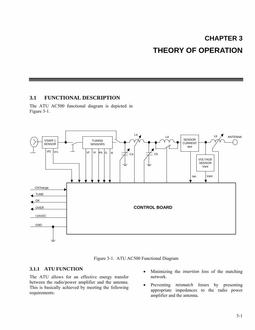
3.1 FUNCTIONAL DESCRIPTION The ATU AC500 functional diagram is depicted in Figure 3-1.
ChChange
TUNE
OK
OVER
+24VDC
GND
Ca
La
Cb
Ld Lb
Vf VrVr1 Ph G R
VSWR 1SENSOR
TUNINGSENSORS
SENSORCURRENT
Iant
VOLTAGESENSOR
Vant
CONTROL BOARD
Vf1
VantIan
ANTENNA
Figure 3-1. ATU AC500 Functional Diagram
3.1.1 ATU FUNCTION The ATU allows for an effective energy transfer between the radio/power amplifier and the antenna. This is basically achieved by meeting the following requirements:
• Minimizing the insertion loss of the matching network.
• Preventing mismatch losses by presenting appropriate impedances to the radio power amplifier and the antenna.
Theory of Operation
3-2
3.1.2 ATU OPERATION The ATU operates in the following modes:
• Set-up in reset state
• Standby mode
• Matched loop tuning
• Transmission.
Reset state: When setting up in reset state mode, the controller initialization is performed. In this mode, the controller sets its ports into reset state upon power supply turn on. After reset state set-up is completed, the controller enters standby mode.
Matched loop tuning: Tuning mode starts when 3-5 msec positive "ChChange" control pulse is applied to the circuit. At the end of "ChChange" pulse, the ATU controller switches on the tuning sensor using "DD1" command. This low level signal is received from ATU through "TUNE" circuit and is sent to the transmitter that initializes 3-14 W RF signal at the transmitter output. The transmitter output is transferred to the ATU input and then to the frequency meter and tuning sensor TS5.281 inputs.
The frequency meter measures transmitter’s RF signal frequency and defines the record/recovery channel number of the matched loop LC cell from the ATU control board nonvolatile memory. Appropriate LC elements are switched on, forward and reflected wave voltages are measured by the tuning sensor and VSWR is calculated.
If VSWR is less than 1.5 then tuning process signal "TUNE" is switched off (control signal applied to "TUNE" circuit is set up to high level) by switching off RF power at ATU input. "DD1" command is turned off (tuning sensor is off) by the ATU "OK" low level signal, that indicates ATU tuning has been completed, and the controller enters standby mode.
If VSWR is higher than 1.5 then matched loop tuning process starts using LC elements commutation in accordance with the tuning algorithm.
Tuning sensor TS5.281 provides error signals as follows:
• Ph - error by phase
• R - error by active resistance
• G - error by active conductance
• Error by value of forward (Vf) and reflected (Vr) waves.
These signals define the level and type of the matched loop disparity by phase, active resistance, active conductance and VSWR.
The signals received from sensor board TS5.281 are transferred to control board TS5.283.
If ATU is tuned with an antenna controlled by a matched loop current and voltage out of limits, then simultaneously with the low level “OK” signal applied to “OVER” circuit, a signal is transferred to the transmitter for signalizing transmitter power reduction to 200-250 W. At this stage the tuning mode is completed.
Transmission: The transmission mode starts immediately after the matched loop tuning has been completed. Once RF power is received at the ATU input, the controller starts to control ATU status using Vf1 forward wave sensor. During this stage, the controlled forward (Vf1) and reflected (Vr1) waves level is measured and VSWR1 is calculated. Additionally, antenna current Iant and antenna input voltage Vant are measured and the temperature sensor S1 is controlled.
If VSWR1 is greater than 2, or Iant and Vant are out of limits, or S1 temperature sensor is triggered, then a low level signal is transferred from the “OVER” circuit to the transmitter, signalizing to reduce transmitter power to 200-250 W. When this stage is completed, the ATU controller switches to standby mode.
3.2 ELECTRICAL DIAGRAMS DESCRIPTION
The ATU electrical diagrams are depicted in Appendix A.
3.2.1 TUNING SENSORS BOARD TS5.281 (see Electrical Diagram TS5.281 - TBD)
The Tuning Sensors TS5.281 comprise:
• Standing wave sensor (SWR1)
• Standing wave sensor (SWR)
• Phase sensor
• Active conductance sensor
• Active resistance sensor

Theory of Operation
3-3
• Matched loop input capacitors group.
The standing wave sensor (SWR1) is used for ATU operation control when input power is up to 500 W.
The standing wave sensor (SWR), phase sensor, active conductance sensor and active resistance sensor are used for ATU tuning when input power is between 3-14 W. These sensors are switched on for tuning the ATU when K4, K12 relays are activated by the "DD1" circuit.
The RF voltage is transferred from resistor R41 through connector J2 to the frequency meter that is located on the control board TS5.283.
3.2.1.1 Standing Wave Sensor (SWR1)
The standing wave sensor (SWR1) consists of forward wave and reflected wave sensors.
SWR1 sensor consists of a capacitive voltage divider with C3, C4, C7 capacitors, a current transformer T1, R3, R5 resistors and two diode detectors D1, D3.
When the load is 50 Ω, the capacitor C7 voltage is equal to the R3, R5 resistors voltages. The R3, R5 resistors voltages are at opposite phase, meaning that D1 diode input voltages are summed, D3 diode input voltages are deducted and the resulting total voltage equals to zero. These voltages are detected by the diodes and are transferred to the sensor input via Vf1, Vr1 circuits.
When the load is other than 50 Ω, the C7 capacitor voltage is not equal to R3, R5 resistors voltages. The R3, R5 resistors voltages are at opposite phase, meaning D1 diode input voltages are summed and D3 diode input voltages are deducted but the resulting voltage in this case, is not equal to zero.
When the load consists of 50 Ω resistive load, combined with inductive or capacitive component connected serially or in parallel, the voltage on C7 capacitor is not in-phase to the R3, R5 resistors voltages, meaning D1 diode input voltages are summed and D3 diode input voltages are deducted but the resulting voltage in this case, is not equal to zero.
The signals "Vf1" and "Vr1" are transferred to ADC circuits in TS5.283 controller. The ADC digital data serves for standing wave ratio SWR1 calculation based on following formula:
r1f1
r1f1
VVVV
SWR1−+
=
3.2.1.2 Standing Wave Sensor (SWR)
The standing wave sensor (SWR) consists of forward wave and reflected wave sensors.
SWR sensor consists of capacitive voltage divider C27, C31, C42 capacitors, a current transformer T3 and R21, R23 resistors and two diode detectors D7, D9. The SWR sensor operates by the same principle as SWR1 sensor.
The standing wave ratio SWR is calculated using the following formula:
rf
rf
VVVV
SWR1−+
=
3.2.1.3 Phase Sensor
The phase sensor consists of a voltage divider with C26, C28, R14, R15, L2 components, a current transformer T2, R12, R16 resistors, two diode detectors D5, D6 and a balance unit with R11, R13, R18 resistors.
When it is connected to 50 Ω load, the R12, R16 resistors voltages are equal to each other and 90 degrees phase displaced relative to R14, R15 resistors voltages, meaning that D5, D6 diode input voltages are equal. The output diode voltages (Ph+, Ph-) are equal as well.
These voltages are transferred to sensor’s output connector J1.
When it is connected to a complex load that includes a reactive component, the R12, R16 resistors voltages are phase displaced relative to R14, R15 resistors voltages, with an angle different than 90 degrees. It means that D5, D6 diode input voltages are not equal and the diode output voltages are not equal either.
If the reactive component of the load has inductive characteristics, the output voltage Ph+ is higher than Ph- output voltage, and if the reactive component has capacitive characteristics, the output voltage Ph+ is less than Ph- output voltage.
When it works at frequencies higher than 7 MHz, the VPh circuit outputs a signal that switches K4 relay to on. The relay contacts short the R15 resistor, and therefore the D5, D6 diode voltages are reduced to a permissible level.

Theory of Operation
3-4
3.2.1.4 Active Conductance Sensor
The active conductance sensor consists of capacitive voltage divider C67, C71, C55, a current transformer T4, resistor R31, two diode detectors D10, D11 and a balance circuit with R29, R30, R33 resistors.
When it is connected to a 50 Ω load, the voltage on C55 capacitor is twice higher than the voltage on R31 resistor. These voltages are out of phase, meaning D10, D11 diode input voltages are equal and output diode voltages (G+, G-) are equal as well. These voltages are transferred to the sensor’s outputs.
When it is connected to a load higher than 50 Ω, the voltage on C55 capacitor increases, and the voltage on resistor R31 decreases, meaning that the voltage (G+) increases at D10 diode output and voltage (G-) decreases at D11 diode output.
When it is connected to a load less than 50 Ω, the voltage on C55 capacitor decreases and the voltage on resistor R31 increases, meaning that the voltage (G+) decreases on D10 diode output and the voltage (G-) increases at D11 diode output.
When it is connected to a 50 Ω load, with inductive or capacitive component connected to the load in parallel, the D10, D11 diode input voltages remain equal and diode output voltages are equal as well.
3.2.1.5 Active Resistance Sensor
An active resistance sensor consists of capacitive voltage divider based on C62, C69, C72 capacitors and a current transformer T5, resistors R37, R38, two diode detectors D12, D13 and a balance circuit based on R35, R36, R40 resistors.
When it is connected to a 50 Ω load, the voltage on C62 capacitor is twice less than the voltage on R37, R38 resistors and these voltages are out-of phase, meaning that D12, D13 diode input voltages are equal and these diodes output voltages (R+, R-) are equal as well. These voltages are transferred to the sensor’s output.
When operating with a load higher than 50 Ω, the voltage on capacitor C62 increases and the voltage on resistors R37, R38 decreases, meaning that D12 diode output voltage (R+) increases and D13 diode output voltage (R-) decreases.
When operating with a load less than 50 Ω, the voltage on capacitor C62 decreases and the voltage on resistors R37, R38 increases, meaning that D12 diode output
voltage (R+) decreases and D13 diode output voltage (R-) increases.
When operating with a 50 Ω load and inductance or capacity component serially connected to it, D12, D13 diode input voltages remain equal and the diode output voltages are equal as well.
3.2.1.6 Matched Loop Input Capacitors Group
This group is formed by a discretely switched set of capacitors with values changed in a binary order. The operation of this group of capacitors is described in the following “Matched Loop” section.
3.2.2 MATCHED LOOP BOARD TS5.282 (See Electrical Diagram TS5.282 - TBD)
The Matched loop board TS5.282 consists of the following parts:
• U-shaped loop
• Antenna current and voltage sensors
• Filters for interference suppression.
The transformation of antenna-feeder circuit is provided by a U-shaped circuit formed by a group of input capacitors, group of input inductances and a group of input capacitors switched by electromagnetic relays K1 to K25.
The group of input capacitors on TS5.281 board, is switched by an electromagnetic relay using commands "C1"-"C9".
The group of output capacitors is formed by a discretely switched set of capacitors C8, C14, C20, C25, C30, C36, with values changed in binary order.
The group of output capacitors is switched by electromagnetic relays using commands "С11"-С16".
The group of inductances is formed by a discretely switched set of inductances L19 to L26 and L28. The group of inductances L19 to L26 has values that are chosen in binary order.
The group of inductances L19 to L26 is used for tuning the frequency range of 4.0-30.0 MHz and the precise tuning range of 1.6-30.0 MHz. The main tuning of the frequency range 1.5-4.0 MHz, is performed using the inductances L1 and L2, located in the unit’s case.
The group of inductances L19 to L26 and L28 is switched by electromagnetic relays using commands "L1"-L8" and “Ld”.

Theory of Operation
3-5
In frequency range 20-30 MHz, if the circuit resonance frequency (formed by load inductive resistance and assembly parasite capacity), interferes with transmitter working frequency, then additional inductance L28 is connected serially with unit’s output by “Ld” command using relays K24 and K25.
The relay windings K1 to K25 are grounded by capacitors for decreasing high frequency effects. Additionally, HF chokes are connected serially, for decreasing pulse interference during switching and HF interference during emission operation.
The ATU power supply voltage of +24 V is fed through an interference filter using С1, C6, C9, L17, L18 components.
3.2.2.1 Matched Loop Tuning Process
The matched loop tuning process is depicted in Figure 3-2.
The input resistance values are shown in Ra and Xa coordinates, divided by fields defined using sensors specifications Ph, R, G. Before the tuning process is started, groups of input and output capacitors are disconnected and inductances are shorted.
If Za point, indicating antenna input resistance, moves by the indicated path in the chart to the Z1 point, it
means that the capacitors "С11"-"С16" are switched serially one-by-one.
Then, if Z1 point, indicating input resistance of the matched loop, moves to point Z2, that lies at circle-characteristics of conductance sensor G, it means that "L1"-"L14" inductances are switched (opened) one-by-one. Then, if Z2 point, indicating input resistance of the matched loop, moves to point Z3 inside the circle of reflected wave sensor characteristics, it means that the capacitors "С1"-"С9", are connected serially. That is compatible with an input resistance of 50 Ω at SWR not more than 1.3, and the matched loop tuning process ends.
When operating at HF emission, the U-shaped loop voltage is transferred via capacitors divider С43, С44 to diode D1 detector. The detected voltage is output at J1 connector and is transferred to the control board TS5.283 by circuit “Vant”.
The HF voltage, that is proportional to U-shaped loop HF current, is transferred from secondary winding of T1 transformer to D2 diode detector. The detected voltage is output at J1 connector and is transferred to the control board TS5.283.

Theory of Operation
3-6
Z2
Za
R=0
Ph=0
Ph=1
G=1
G=0
0
+Xa
RaRa
R=1
Z1
Z3
Figure 3-2. Tuning Chart
3.2.3 CONTROL BOARD TS5.283 (See Electrical Diagram TS5.283 - TBD and Figure 3-3)
The control board TS5.283 is used for ATU operation control.
The control board comprises the following functional blocks:
• Central processor unit (CPU)
• Serial registers
• Amplifiers
• Circuit of CPU starting after the power is turned on
• Serial Communication Converter UART to RS-232
• Frequency measuring circuit
• Comparators
• EEPROM
• Voltage stabilizer.
The micro-controller AT90S8535 is used as Central Processor Unit (IC U5). The micro-controller AT90S8535 consists of the following:
• Low inherent consumption, 8-channel 10-bit analog-digital converter
• 8Kb of in-circuit re-programmable flash memory (1000 cycles of rewriting)
• 512 bytes of EEPROM (100000 cycles of rewriting)
• 32 programmable input-output lines
• Watchdog timer
• System of internal and external interrupts, 3 timers/counters
• Programmable UART.
Theory of Operation
3-7
Furthermore, the micro-controller has a SLEEP mode that halts the timing oscillator.
To provide quick set-up of ATU, non-volatile EEPROM FM24C16-5 (16 Kb) is used to store ATU settings. It is controlled by a serial bus (SCL, SDA).
Data is received serially from DATA lines and timed by a clock signal CLK. The data is received by registers 74HC595 (IC U11 to U14). Data transmission from internal registers IC U11 to U14 to their external outputs is performed by micro-controller output signals WR1 to WR4.
Registers U11 to U14 output signals are amplified by U11 to U14 amplifiers and U15 to U19 (TPIC2701N). The transistors Q1, Q3, Q5 are used to amplify TUNE, OVER and AM signals.
The analog signals Vf, Vr, Vf1, Vr1, Iant, Uant received from setting sensors via filters are transferred to the analog inputs of the micro-controller. The IC TL431BID (U7) is used to provide a stable reference voltage for the analogue-to-digital converter.
The logic levels of Ph, R, G signals are formatted using the analog signals Ph+, Ph-, R+, R-, G+, G- and the comparator LM2109D.
As the SLEEP mode is activated for radio frequency noises lowering, the interrupt circuits are controlled by the signals ChChange (R34, R30, D4, U4) and Vf1 (R14, C12, U2, R32, R33, R35, R31, C34, U4) and are used for a stable “wake-up”.
The signal received from overheating sensor SW75 via the threshold element 74HC14D (U4) enters the micro-controller.
The IC MAX232EWE (U15) converts UART serial data to RS-232 interface serial data.
The timer T1 converts the frequency-measured signal to the FREQ data that enters the micro-controller. The FREQ signal is converted to TTL level by the transistors Q2 and Q4 and then its frequency is lowered by divider IC EMP7032SL, to a frequency perceptible by the micro-controller.
The controller board TS5.283 is fed by 24 V ± 4 V power supply. To ensure that +5 V voltage conforms with the value required for controller’s ICs operation, the stabilizer MC7805B (U3) is used to decrease the level of radio frequency noise.

Theory of Operation
3-8
CPU AREFVr
Iant
ADCinputs
OVER
TUNE
WR1
WR2
WR3FREQ
CLKDATA
RESET
L1...L9LdC1...C16VphDD1
UART
CHANEL CHANGE
T1
INT0
ff/n
R xDTxD
WR4
INT1
SW75
OK
Vf
Vf1
Vr1
Uant
Vf1
ph+
R+R-G+
ph-
G-
R
G
Ph
RAMSCL
SDA
STU+24V +5V
DD1_Vph_
~~~~~~~~~~~~
= =
Figure 3-3. Control Board TS5.283 Functional Diagram