heterojunction bipolar transistor technology (ingap...
TRANSCRIPT

NOTRECOMMENDEDFORNEW
DESIGN
NOTRECOMMENDEDFORNEW
DESIGN
MMG3002NT1
1RF Device DataFreescale Semiconductor, Inc.
MMG3002NT1
40--3600 MHz, 20 dB21 dBm
InGaP HBT GPA
Heterojunction Bipolar TransistorTechnology (InGaP HBT)Broadband High Linearity AmplifierThe MMG3002NT1 is a general purpose amplifier that is internally input
and output matched. It is designed for a broad range of Class A, small--signal, high linearity, general purpose applications. It is suitable forapplications with frequencies from 40 to 3600 MHz such as cellular, PCS,BWA, WLL, PHS, CATV, VHF, UHF, UMTS and general small--signal RF.
Features Frequency: 40--3600 MHz P1dB: 21 dBm @ 900 MHz Small--Signal Gain: 20 dB @ 900 MHz Third Order Output Intercept Point: 37.5 dBm @ 900 MHz Single Voltage Supply Internally Matched to 50 Ohms Cost--effective SOT--89 Surface Mount Plastic Package In Tape and Reel. T1 Suffix = 1,000 Units, 12 mm Tape Width, 7--inch Reel.
SOT--89
Table 1. Typical Performance (1)
Characteristic Symbol900MHz
2140MHz
3500MHz Unit
Small--Signal Gain(S21)
Gp 20 18 14.5 dB
Input Return Loss(S11)
IRL --16 --26 --16 dB
Output Return Loss(S22)
ORL --12 --8 --11 dB
Power Output @1dB Compression
P1dB 21 21 18.5 dBm
Third Order OutputIntercept Point
OIP3 37.5 36 32 dBm
1. VCC = 5.2 Vdc, TA = 25C, 50 ohm system.
Table 2. Maximum Ratings
Rating Symbol Value Unit
Supply Voltage VCC 7 V
Supply Current ICC 400 mA
RF Input Power Pin 12 dBm
Storage Temperature Range Tstg --65 to +150 C
Junction Temperature TJ 175 C
Table 3. Thermal Characteristics
Characteristic Symbol Value (2) Unit
Thermal Resistance, Junction to CaseCase Temperature 118C, 5.2 Vdc, 110 mA, no RF applied
RJC 46.5 C/W
2. Refer to AN1955, Thermal Measurement Methodology of RF Power Amplifiers. Go to http://www.freescale.com/rf.Select Documentation/Application Notes -- AN1955.
Document Number: MMG3002NT1Rev. 12, 9/2014
Freescale SemiconductorTechnical Data
Freescale Semiconductor, Inc., 2004--2008, 2012, 2014. All rights reserved.

NOTRECOMMENDEDFORNEW
DESIGN
NOTRECOMMENDEDFORNEW
DESIGN
2RF Device Data
Freescale Semiconductor, Inc.
MMG3002NT1
Table 4. Electrical Characteristics (VCC = 5.2 Vdc, 900 MHz, TA = 25C, 50 ohm system, in Freescale Application Circuit)
Characteristic Symbol Min Typ Max Unit
Small--Signal Gain (S21) Gp 19.3 20 — dB
Input Return Loss (S11) IRL — --16 — dB
Output Return Loss (S22) ORL — --12 — dB
Power Output @ 1dB Compression P1dB — 21 — dBm
Third Order Output Intercept Point OIP3 — 37.5 — dBm
Noise Figure NF — 4.2 — dB
Supply Current ICC 95 110 125 mA
Supply Voltage VCC — 5.2 — V
Table 5. Functional Pin Description
PinNumber Pin Function
1 RFin
2 Ground
3 RFout/DC Supply
Table 6. ESD Protection Characteristics
Test Conditions/Test Methodology Class
Human Body Model (per JESD 22--A114) 1B
Machine Model (per EIA/JESD 22--A115) A
Charge Device Model (per JESD 22--C101) IV
Table 7. Moisture Sensitivity Level
Test Methodology Rating Package Peak Temperature Unit
Per JESD 22--A113, IPC/JEDEC J--STD--020 1 260 C
Figure 1. Functional Diagram
321
2
NOTRECOMMENDEDFORNEW
DESIGN
NOTRECOMMENDEDFORNEW
DESIGN
MMG3002NT1
3RF Device DataFreescale Semiconductor, Inc.
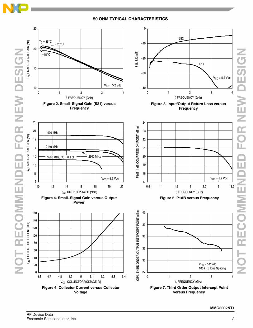
50 OHM TYPICAL CHARACTERISTICS
10
25
0
TC = 85C
f, FREQUENCY (GHz)
Figure 2. Small--Signal Gain (S21) versusFrequency
20
15
1 2 3 4
Gp,SM
ALL--SIGNAL
GAIN(dB)
25C
--40C
4--40
0
0
S22
f, FREQUENCY (GHz)
Figure 3. Input/Output Return Loss versusFrequency
S11
--10
--20
--30
1 2 3
S11,S22(dB)
22
9
23
10
Pout, OUTPUT POWER (dBm)
Figure 4. Small--Signal Gain versus OutputPower
21
19
17
15
13
12 14 16
Gp,SM
ALL--SIGNAL
GAIN(dB)
900 MHz
11
18
3500 MHz, C5 = 0.1 pF
2140 MHz
3.532.521.510.517
24
23
22
20
18
f, FREQUENCY (GHz)
Figure 5. P1dB versus Frequency
P1dB,1dB
COMPRESSIONPOINT(dBm
)
21
19
5.40
160
4.6
VCC, COLLECTOR VOLTAGE (V)
Figure 6. Collector Current versus CollectorVoltage
80
60
20
4.7 5.1 5.2
I CC,COLLECTORCURRENT(mA)
40
4.8 4.9 5 5.3 427
42
0
f, FREQUENCY (GHz)
Figure 7. Third Order Output Intercept Pointversus Frequency
39
36
33
30
1 2 3
VCC = 5.2 Vdc100 kHz Tone Spacing
OIP3,THIRDORDER
OUTPUTINTERCEPTPOINT(dBm
)
20
140
120
100
VCC = 5.2 Vdc
2600 MHz
VCC = 5.2 Vdc
VCC = 5.2 Vdc VCC = 5.2 Vdc

NOTRECOMMENDEDFORNEW
DESIGN
NOTRECOMMENDEDFORNEW
DESIGN
4RF Device Data
Freescale Semiconductor, Inc.
MMG3002NT1
50 OHM TYPICAL CHARACTERISTICS
27
42
5
VCC, COLLECTOR VOLTAGE (V)
Figure 8. Third Order Output Intercept Pointversus Collector Voltage
39
36
33
30
OIP3,THIRDORDER
OUTPUTINTERCEPTPOINT(dBm
)
5.1 5.2 5.45.3
f = 900 MHz100 kHz Tone Spacing
100--40 --20 0 20 40 60 8035
41
T, TEMPERATURE (_C)
Figure 9. Third Order Output Intercept Pointversus Case Temperature
40
39
38
37
OIP3,THIRDORDER
OUTPUTINTERCEPTPOINT(dBm
)
36
Figure 10. Third Order Intermodulation Distortionversus Output Power
Pout, OUTPUT POWER (dBm)
IMD,THIRDORDER
INTERMODULATIONDISTORTION(dBc)
215 7 9 11 13--80
--30
--50
--60
--70VCC = 5.2 Vdcf = 900 MHz100 kHz Tone Spacing
--40
15 150102
105
120
Figure 11. MTTF versus Junction Temperature
103
125 130 135 140 145
TJ, JUNCTION TEMPERATURE (C)
NOTE: The MTTF is calculated with VCC = 5.2 Vdc, ICC = 110 mA
MTTF(YEARS)
40
8
0
f, FREQUENCY (GHz)
Figure 12. Noise Figure versus Frequency
6
4
2
1 2 3
NF,NOISEFIGURE(dB)
0.5 1.5 2.5 3.5 19
--70
--20
9
Pout, OUTPUT POWER (dBm)
Figure 13. Single--Carrier W--CDMA AdjacentChannel Power Ratio versus Output Power
--30
--40
--50
--60
17151311
ACPR,ADJACENTCHANNEL
POWER
RATIO(dBc)
VCC = 5.2 Vdc,f = 900 MHz100 kHz Tone Spacing8 Vdc Supply with 25Ω Dropping Resistor
17 19
104
VCC = 5.2 Vdc
VCC = 5.2 Vdc, f = 2140 MHzSingle--Carrier W--CDMA, 3.84 MHz Channel BandwidthInput Signal PAR = 8.5 dB @ 0.01% Probability (CCDF)

NOTRECOMMENDEDFORNEW
DESIGN
NOTRECOMMENDEDFORNEW
DESIGN
MMG3002NT1
5RF Device DataFreescale Semiconductor, Inc.
50 OHM APPLICATION CIRCUIT: 40--800 MHz
Figure 14. 50 Ohm Test Circuit Schematic
RFOUTPUT
RFINPUT
VSUPPLY
C3 C4
Z1 Z2
C1
Z5
C2
R1
L1
VCC
Z4Z3DUT
Figure 15. S21, S11 and S22 versus Frequency
--40
30
0
f, FREQUENCY (MHz)
S22
200 400 600 800
20
10
0
--10
--20
--30
Figure 16. 50 Ohm Test Circuit Component Layout
C1
L1
C2
R1
C4C3
Z1, Z5 0.347 x 0.058 MicrostripZ2 0.575 x 0.058 MicrostripZ3 0.172 x 0.058 Microstrip
Z4 0.403 x 0.058 MicrostripPCB Getek Grade ML200C, 0.031, r = 4.1
S21,S11,S22(dB)
S21
S11
MMG30XXRev 2
VCC = 5.2 Vdc
Table 8. 50 Ohm Test Circuit Component Designations and ValuesPart Description Part Number Manufacturer
C1, C2 0.01 F Chip Capacitors C0603C103J5RAC Kemet
C3 0.1 F Chip Capacitor C0603C104J5RAC Kemet
C4 1 F Chip Capacitor C0603C105J5RAC Kemet
L1 470 nH Chip Inductor BK2125HM471--T Taiyo Yuden
R1 7.5 Ω Chip Resistor RK73B2ATTE7R5J KOA Speer
Table 9. Supply Voltage versus R1 Values
Supply Voltage 6 7 8 9 10 11 12 V
R1 Value 7.3 16 25 35 44 53 62
Note: To provide VCC = 5.2 Vdc and ICC = 110 mA at the device.

NOTRECOMMENDEDFORNEW
DESIGN
NOTRECOMMENDEDFORNEW
DESIGN
6RF Device Data
Freescale Semiconductor, Inc.
MMG3002NT1
50 OHM APPLICATION CIRCUIT: 800--3400 MHz
Figure 17. 50 Ohm Test Circuit Schematic
RFOUTPUT
RFINPUT
VSUPPLY
C3 C4
Z1 Z2
C1
Z5
C2
R1
L1
VCC
Z4Z3DUT
Figure 18. S21, S11 and S22 versus Frequency
--30
30
f, FREQUENCY (MHz)
S22
1200
20
10
0
--10
--20
Figure 19. 50 Ohm Test Circuit Component Layout
C1
L1
C2
R1
C4C3
Z1, Z5 0.347 x 0.058 MicrostripZ2 0.575 x 0.058 MicrostripZ3 0.172 x 0.058 Microstrip
Z4 0.403 x 0.058 MicrostripPCB Getek Grade ML200C, 0.031, r = 4.1
S21,S11,S22(dB)
S21
S11
1600800 2000 2400 2800 3200 3600
MMG30XXRev 2VCC = 5.2 Vdc
Table 10. 50 Ohm Test Circuit Component Designations and ValuesPart Description Part Number Manufacturer
C1, C2 150 pF Chip Capacitors C0603C151J5RAC Kemet
C3 0.1 F Chip Capacitor C0603C104J5RAC Kemet
C4 1 F Chip Capacitor C0603C105J5RAC Kemet
L1 56 nH Chip Inductor HK160856NJ--T Taiyo Yuden
R1 7.5 Ω Chip Resistor RK73B2ATTE7R5J KOA Speer

NOTRECOMMENDEDFORNEW
DESIGN
NOTRECOMMENDEDFORNEW
DESIGN
MMG3002NT1
7RF Device DataFreescale Semiconductor, Inc.
50 OHM APPLICATION CIRCUIT: 3400--3600 MHz
C1
L1
C2
R1
C5
C4C3
37003200 3300 3800
Figure 20. 50 Ohm Test Circuit Schematic
Figure 21. S21, S11 and S22 versus Frequency
f, FREQUENCY (MHz)
Figure 22. 50 Ohm Test Circuit Component Layout
--30
20
S22
10
0
--10
--20
S21,S11,S22(dB)
S21
S11
RFOUTPUT
RFINPUT
VSUPPLY
C3 C4
Z1 Z2
C1
Z6
C2
R1
L1
VCC
Z5Z3DUT
Z1, Z6 0.347 x 0.058 MicrostripZ2 0.575 x 0.058 MicrostripZ3 0.086 x 0.058 Microstrip
Z4 0.085 x 0.058 MicrostripZ5 0.404 x 0.058 MicrostripPCB Getek Grade ML200C, 0.031, r = 4.1
3400 3500 3600
Z4
C5
MMG30XXRev 2
VCC = 5.2 Vdc
Table 11. 50 Ohm Test Circuit Component Designations and ValuesPart Description Part Number Manufacturer
C1, C2 150 pF Chip Capacitors C0603C151J5RAC Kemet
C3 0.1 F Chip Capacitor C0603C104J5RAC Kemet
C4 1 F Chip Capacitor C0603C105J5RAC Kemet
C5 (1) 0.1 pF Chip Capacitor 06035J0R1BS AVX
L1 39 nH Chip Inductor HK160839NJ--T Taiyo Yuden
R1 7.5 Ω Chip Resistor RK73B2ATTE7R5J KOA Speer
1. Tuning capacitor: Capacitor value and location on the transmission line are varied for different frequencies.

NOTRECOMMENDEDFORNEW
DESIGN
NOTRECOMMENDEDFORNEW
DESIGN
8RF Device Data
Freescale Semiconductor, Inc.
MMG3002NT1
50 OHM TYPICAL CHARACTERISTICS
Table 12. Common Emitter S--Parameters (VCC = 5.2 Vdc, TA = 25C, 50 Ohm System)
fMHz
S11 S21 S12 S22
|S11| |S21| |S12| |S22|
100 0.05966 176.181 10.25158 174.805 0.07235 --0.722 0.04946 --167.612
150 0.07228 --178.627 9.96687 171.111 0.07071 --1.821 0.0953 --129.396
200 0.09041 151.476 10.46556 167.719 0.07464 --3.053 0.05913 --124.668
250 0.0909 149.96 10.36837 164.949 0.07424 --3.553 0.08015 --125.378
300 0.08882 145.472 10.30366 162.017 0.07406 --4.277 0.09694 --122.814
350 0.08508 140.833 10.2505 158.995 0.07407 --4.934 0.11062 --121.876
400 0.08377 136.078 10.17971 156.158 0.07405 --5.7 0.12723 --122.007
450 0.08191 131.492 10.10383 153.293 0.07365 --6.307 0.14156 --122.555
500 0.07982 125.857 10.02536 150.437 0.07358 --7.037 0.15558 --123.436
550 0.07776 120.816 9.94165 147.642 0.07346 --7.676 0.1685 --124.8
600 0.0773 115.435 9.85596 144.898 0.07336 --8.2 0.18177 --126.796
650 0.07677 110.371 9.76098 142.109 0.07321 --8.911 0.19472 --128.506
700 0.07664 104.874 9.6623 139.374 0.07301 --9.464 0.20662 --130.47
750 0.07628 100.112 9.56168 136.692 0.0729 --10.069 0.21833 --132.663
800 0.07619 95.73 9.45426 134.024 0.07275 --10.618 0.22977 --134.835
850 0.07601 91.72 9.34921 131.391 0.07273 --11.184 0.24125 --137.084
900 0.07567 87.313 9.23967 128.792 0.07257 --11.821 0.25232 --139.685
950 0.07642 83.036 9.13144 126.149 0.07238 --12.312 0.26303 --142.257
1000 0.07619 80.021 9.01205 123.659 0.07228 --12.88 0.27394 --144.736
1050 0.07666 76.201 8.90327 121.137 0.07218 --13.474 0.28332 --147.346
1100 0.07678 73.008 8.78013 118.657 0.07202 --13.93 0.29417 --150.042
1150 0.07673 70.68 8.66342 116.191 0.0719 --14.519 0.30394 --152.767
1200 0.07674 68.773 8.53991 113.779 0.07178 --15.062 0.31393 --155.358
1250 0.07628 66.216 8.42251 111.392 0.07176 --15.551 0.32286 --157.992
1300 0.07618 64.635 8.30514 109.034 0.07164 --16.115 0.33259 --160.483
1350 0.07454 62.959 8.18109 106.673 0.07149 --16.539 0.34127 --162.981
1400 0.07373 60.65 8.06498 104.367 0.07152 --17.114 0.34972 --165.377
1450 0.0724 59.062 7.94403 102.073 0.07137 --17.565 0.35931 --167.823
1500 0.06466 48.656 7.85198 99.72 0.0715 --18.187 0.35762 --170.82
1550 0.0646 44.563 7.73641 97.503 0.07167 --18.755 0.36484 --172.845
1600 0.06495 39.856 7.63068 95.372 0.07161 --19.217 0.37158 --174.751
1650 0.0657 35.953 7.52257 93.247 0.07165 --19.614 0.37821 --176.697
1700 0.06599 31.949 7.43591 91.089 0.07171 --20.239 0.38558 --178.85
1750 0.0666 28.693 7.31976 88.981 0.07168 --20.731 0.39036 179.588
1800 0.06649 25.448 7.22121 86.872 0.07176 --21.241 0.39732 177.775
1850 0.06637 22.687 7.11782 84.83 0.07181 --21.685 0.40211 175.992
1900 0.06563 19.369 7.01794 82.771 0.07188 --22.233 0.40749 174.294
1950 0.06514 15.516 6.91688 80.824 0.07197 --22.678 0.41306 172.684
2000 0.0641 13.294 6.82126 78.739 0.07217 --23.218 0.41825 170.97
2050 0.06323 9.843 6.72865 76.797 0.07214 --23.632 0.42367 169.372
2100 0.06288 6.976 6.63794 74.849 0.07234 --24.15 0.42905 167.644
2150 0.06195 4.218 6.55483 72.888 0.07244 --24.689 0.43442 166.014
2200 0.06084 2.075 6.46275 70.939 0.07265 --25.273 0.43857 164.274
2250 0.05942 --0.3 6.37821 69.013 0.07275 --25.755 0.44419 162.598
(continued)

NOTRECOMMENDEDFORNEW
DESIGN
NOTRECOMMENDEDFORNEW
DESIGN
MMG3002NT1
9RF Device DataFreescale Semiconductor, Inc.
50 OHM TYPICAL CHARACTERISTICS
Table 12. Common Emitter S--Parameters (VCC = 5.2 Vdc, TA = 25C, 50 Ohm System) (continued)
fMHz
S11 S21 S12 S22
|S11| |S21| |S12| |S22|
2300 0.05808 --2.187 6.29055 67.098 0.07295 --26.316 0.44756 160.879
2350 0.05526 --4.038 6.20851 65.179 0.07318 --26.813 0.45231 159.11
2400 0.05338 --6.096 6.12256 63.315 0.07337 --27.387 0.45571 157.425
2450 0.05054 --7.643 6.04461 61.45 0.07359 --27.903 0.46063 155.679
2500 0.04768 --10.036 5.96594 59.564 0.07386 --28.462 0.46419 153.884
2550 0.04494 --12.811 5.88833 57.733 0.07416 --29.19 0.4681 152.005
2600 0.04239 --14.731 5.81782 55.868 0.07435 --29.754 0.47249 150.142
2650 0.0393 --16.676 5.74121 53.98 0.07445 --30.312 0.47601 148.126
2700 0.03707 --20.889 5.66538 52.04 0.0748 --31.053 0.47991 146.214
2750 0.0346 --21.7 5.59155 50.247 0.07499 --31.654 0.48371 144.147
2800 0.03163 --24.056 5.51967 48.401 0.07519 --32.344 0.48777 142.183
2850 0.02869 --26.756 5.44631 46.54 0.0754 --33.048 0.49144 140.072
2900 0.02667 --28.324 5.37422 44.74 0.07563 --33.749 0.4961 138.081
2950 0.02324 --29.457 5.30336 42.914 0.07577 --34.431 0.50017 136.001
3000 0.02069 --34.403 5.23613 41.138 0.07596 --35.209 0.5054 133.872
3050 0.01861 --37.625 5.16698 39.322 0.07624 --35.917 0.50901 131.91
3100 0.01563 --41.101 5.09908 37.495 0.07648 --36.648 0.51431 129.855
3150 0.01407 --49.967 5.03148 35.696 0.0766 --37.389 0.51844 127.844
3200 0.01296 --54.052 4.96452 33.935 0.07684 --38.12 0.52333 125.818
3250 0.01129 --59.44 4.89769 32.159 0.07708 --38.894 0.52814 123.86
3300 0.01031 --67.904 4.83271 30.407 0.07721 --39.663 0.53368 121.891
3350 0.00977 --71.657 4.76883 28.702 0.07742 --40.479 0.53765 120.096
3400 0.00821 --77.779 4.707 26.984 0.07764 --41.116 0.54299 118.206
3450 0.0076 --90.054 4.64886 25.288 0.07774 --41.964 0.54702 116.357
3500 0.0074 --97.151 4.59041 23.575 0.07797 --42.707 0.55121 114.75
3550 0.00666 --114.876 4.5319 21.885 0.07819 --43.538 0.55593 113.11
3600 0.00749 --127.171 4.47455 20.231 0.07843 --44.293 0.55935 111.522
NOTRECOMMENDEDFORNEW
DESIGN
NOTRECOMMENDEDFORNEW
DESIGN
10RF Device Data
Freescale Semiconductor, Inc.
MMG3002NT1
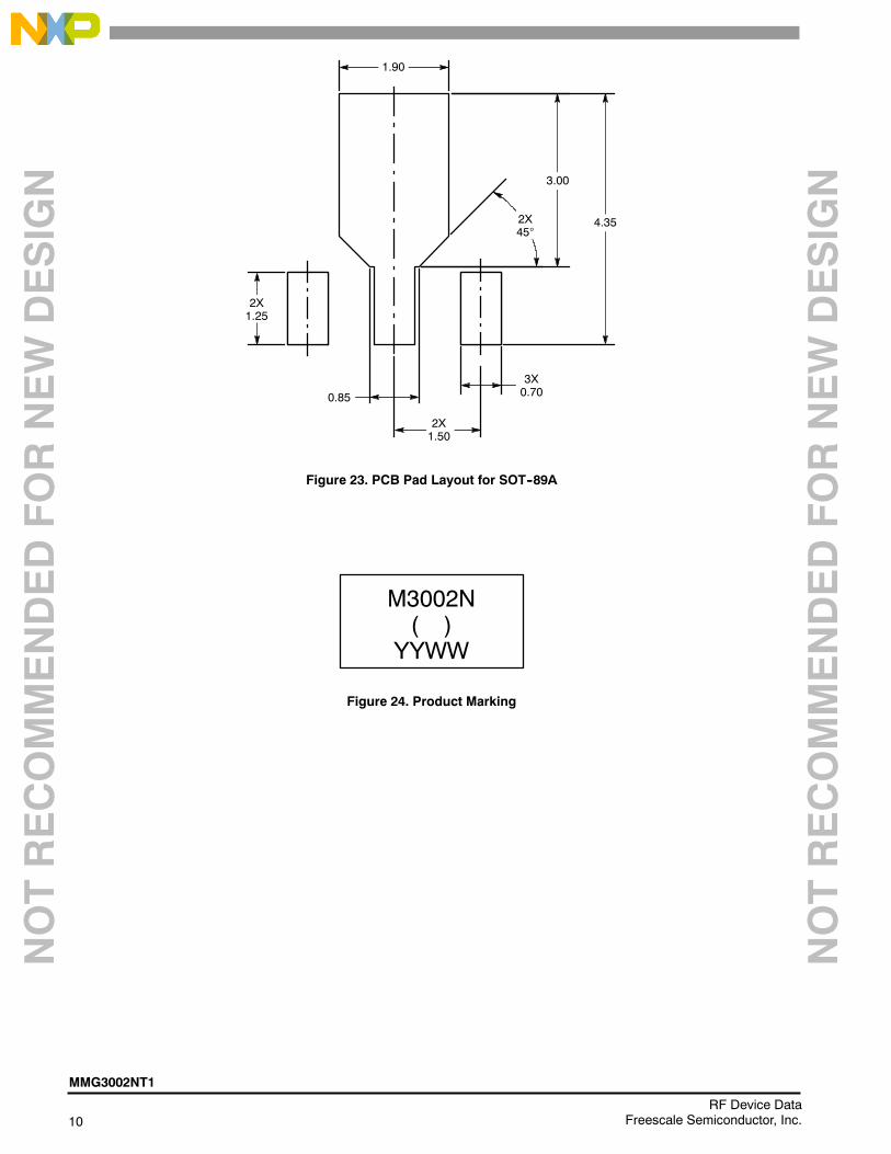
Figure 23. PCB Pad Layout for SOT--89A
4.35
3.00
2X45
3X0.70
2X1.50
0.85
2X1.25
1.90
Figure 24. Product Marking
M3002N( )
YYWW

NOTRECOMMENDEDFORNEW
DESIGN
NOTRECOMMENDEDFORNEW
DESIGN
MMG3002NT1
11RF Device DataFreescale Semiconductor, Inc.
PACKAGE DIMENSIONS

NOTRECOMMENDEDFORNEW
DESIGN
NOTRECOMMENDEDFORNEW
DESIGN
12RF Device Data
Freescale Semiconductor, Inc.
MMG3002NT1

NOTRECOMMENDEDFORNEW
DESIGN
NOTRECOMMENDEDFORNEW
DESIGN
MMG3002NT1
13RF Device DataFreescale Semiconductor, Inc.

NOTRECOMMENDEDFORNEW
DESIGN
NOTRECOMMENDEDFORNEW
DESIGN
14RF Device Data
Freescale Semiconductor, Inc.
MMG3002NT1
PRODUCT DOCUMENTATION AND SOFTWARE
Refer to the following resources to aid your design process.
Application Notes
AN1955: Thermal Measurement Methodology of RF Power Amplifiers AN3100: General Purpose Amplifier and MMIC BiasingSoftware
.s2p File
For Software, do a Part Number search at http://www.freescale.com, and select the “Part Number” link. Go to Software &Tools on the part’s Product Summary page to download the respective tool.
FAILURE ANALYSIS
At this time, because of the physical characteristics of the part, failure analysis is limited to electrical signature analysis. Incases where Freescale is contractually obligated to perform failure analysis (FA) services, full FA may be performed by thirdparty vendors with moderate success. For updates contact your local Freescale Sales Office.
REVISION HISTORY
The following table summarizes revisions to this document.
Revision Date Description
7 Mar. 2007 Corrected and updated Part Numbers in Tables 8, 10 and 11, Component Designations and Values, toRoHS compliant part numbers, pp. 6--8
8 July 2007 Replaced Case Outline 1514--01 with 1514--02, Issue D, pp. 1, 12--14. Case updated to add missingdimension for Pin 1 and Pin 3.
9 Mar. 2008 Removed Footnote 2, Continuous voltage and current applied to device, from Table 2, Maximum Ratings,p. 1
Corrected Fig. 13, Single--Carrier W--CDMA Adjacent Channel Power Ratio versus Output Power y--axis(ACPR) unit of measure to dBc, p. 5
Corrected S--Parameter table frequency column label to read “MHz” versus “GHz” and correctedfrequency values from GHz to MHz, pp. 9, 10
10 Feb. 2012 Corrected temperature at which ThetaJC is measured from 25C to 118C and added “no RF applied” toThermal Characteristics table to indicate that thermal characterization is performed under DC test with noRF signal applied, p. 1
Table 6, ESD Protection Characteristics, removed the word “Minimum” after the ESD class rating. ESDratings are characterized during new product development but are not 100% tested during production. ESDratings provided in the data sheet are intended to be used as a guideline when handling ESD sensitivedevices, p. 3
Removed ICC bias callout from applicable graphs and Table 12, Common Emitter S--Parameters headingas bias is not a controlled value, pp. 4–10
Added .s2p File availability to Product Software, p. 15
11 Dec. 2012 Replaced the PCB Pad Layout drawing, the package isometric and mechanical outline for Case 1514--02(SOT--89) with Case 2142--01 (SOT--89) as a result of the device transfer from a Freescale wafer fab to anexternal GaAs wafer fab and new assembly site. The new assembly and test site’s SOT--89 package hasslight dimensional differences, pp. 1, 11--14. Refer to PCN13337, GaAs Fab Transfer.
Added Fig. 24, Product Marking, p. 11
12 Sept. 2014 Table 2, Maximum Ratings: updated Junction Temperature from 150C to 175C to reflect recent testresults of the device, p. 1
Added Failure Analysis information, p. 14
NOTRECOMMENDEDFORNEW
DESIGN
NOTRECOMMENDEDFORNEW
DESIGN
MMG3002NT1
15RF Device DataFreescale Semiconductor, Inc.
Information in this document is provided solely to enable system and softwareimplementers to use Freescale products. There are no express or implied copyrightlicenses granted hereunder to design or fabricate any integrated circuits based on theinformation in this document.
Freescale reserves the right to make changes without further notice to any productsherein. Freescale makes no warranty, representation, or guarantee regarding thesuitability of its products for any particular purpose, nor does Freescale assume anyliability arising out of the application or use of any product or circuit, and specificallydisclaims any and all liability, including without limitation consequential or incidentaldamages. “Typical” parameters that may be provided in Freescale data sheets and/orspecifications can and do vary in different applications, and actual performance mayvary over time. All operating parameters, including “typicals,” must be validated foreach customer application by customer’s technical experts. Freescale does not conveyany license under its patent rights nor the rights of others. Freescale sells productspursuant to standard terms and conditions of sale, which can be found at the followingaddress: freescale.com/SalesTermsandConditions.
Freescale and the Freescale logo are trademarks of Freescale Semiconductor, Inc.,Reg. U.S. Pat. & Tm. Off. All other product or service names are the property of theirrespective owners.E 2004--2008, 2012, 2014 Freescale Semiconductor, Inc.
How to Reach Us:
Home Page:freescale.com
Web Support:freescale.com/support
Document Number: MMG3002NT1Rev. 12, 9/2014