heavy ion transient characterization of a hardened … submitted to 2002 ieee nsrec workshop...
TRANSCRIPT
Preprint submitted to 2002 IEEE NSREC Workshop Proceedings
Heavy Ion Transient Characterization of a Hardened-by-Design Active Pixel Sensor Array
Cheryl J. Marshall, Kenneth A. LaBel, Robert A. Reed Code 561
NASA Goddard Space Flight Center Greenbelt, MD 20771 USA
Paul W. Marshall NASA Consultant
7655 Hat Creek Road, Brookneal, VA 24528 USA
Wheaton B. Byers, Christopher Conger, Joe Peden Scientific Applications International Corporation (SAIC)
McLean, VA 22102 USA
El-Sayed Eid Gentex Corporation
600 N. Centennial St., Zeeland, MI 49464 USA
Michael R. Jones, Scott Kniffin Orbital Sciences Corporation Greenbelt, MD 20771 USA
George Gee Stinger Ghaffarian Technologies, Incorporated
Greenbelt, MD 20771 USA
Jim Pickel PR & T, Inc.
Fallbrook, CA 92028 USA
Abstract—This paper presents heavy ion test data on the
single event transient response of an active pixel sensor four quadrant test chip with different radiation tolerant designs in a commercial 0.35 µm CMOS process. The physical design techniques of enclosed geometry and P-type guard rings are used to design the four N-type active photodiode pixels as described in a previous paper [1]. Transient measurements on the 256 x 256 pixel array as a function of Ar ion incidence angle show a significant variation in the amount of charge collected as well as the charge spreading dependent on the pixel type. The results are correlated with processing and design information provided by Photobit. In addition, there is a significant variability
between individual ion strikes for some unit cell designs. No latch-up is observed up to an LET of 106 MeV/mg/cm2.
Keywords—radiation effects; active pixel sensor; single event transients
I. INTRODUCTION Cost-effective radiation tolerant active pixel sensor (APS)
arrays are becoming an important alternative to charge coupled device (CCD) arrays for some space applications without specialized performance requirements such as ultra-low dark currents. The inherent advantages of APS technology result from utilization of standard CMOS processing and include the possibility of highly integrated and functional yet low power imaging systems (i.e. ‘camera-on-a-
We appreciate support from the NASA Electronics Radiation Characterization Project which is a part of the NASA Electronics Parts and Packing Program (NEPP), the Next Generation Space Telescope (NGST)program, and the Defense Threat Reduction Agency (DTRA).

chip’ [2]). Further, since APS pixels are directly addressed there are no proton induced charge transfer losses such as those experienced with CCDs arrays in space.
The radiation tolerance of the present APS sensors up to total ionizing dose levels of 30 Mrad(Si) was reported in [1]. The primary impact of the 60Co gamma irradiation of the devices was a linear increase in the dark current with total ionizing dose at a rate of 1 - 2 pA/cm2/krad(Si) at room temperature dependent on the pixel design. The thin gate oxide (~7.0 nm) contributed to the radiation hardness of all four pixel designs by assuring low voltage threshold shifts.
The purpose of this paper is to investigate the heavy ion response of commercial APS imaging technology and the efficacy of hardening-by-design for transient ion effects. To date there is very little heavy-ion characterization of APS devices. Hopkinson [3] has reported limited latch-up data for a 515 x 512 pixel array fabricated by IMEC, Belgium using the 0.7 µm twin well P-substrate process of Alcatel Microelectronics. No latch-up was observed in the device for 28 MeV/mg/cm2 Ar ions up to a fluence of 2 x 10⁶ ions/cm2 in testing that was limited by beam constraints. Although the analogue-to-digital (ADC) latched as described in [3], the author noted that it was an old design that was slated for replacement.
II. DESCRIPTION OF THE APS TEST CHIP As described in detail in [1], the physical design techniques of enclosed geometry and p-channel guard rings is used to design and lay out a set of four N-type radiation tolerant active photodiode (PD) pixels. The sensor arrays are standard 0.35 µm CMOS technology fabricated with a mixed mode, twin well process with 7.0 nm gate oxides. The 256 x 256 full array has four sub arrays (or quadrants) made up of 16.2 µm by 16.2 µm pixels. The key design features of the test chip are summarized in Table 1.
III. EXPERIMENT DESCRIPTION Tests were performed at the Texas A&M University
cyclotron facility in College Station, TX. Measurements were made using 40Ar at 15.0 MeV/amu, 84Kr at 15.3 MeV/amu, and 131Xe at 15.2 MeV/amu. The present paper focuses on results obtained with 15.0 MeV/amu 40Ar (LET = 8.44 MeV/mg/cm2 at normal incidence) as a function of incident angle.
TABLE I. KEY DESIGN PARAMETERS FOR EACH OF THE FOUR PIXELS
The Ar data has been obtained at three angles of incidence: normal, 60º from normal and 75º from normal. The azimuth angle is not varied. Each test sequence consists of 100 full frames of data acquired with a 0.5 s integration time by reading the imager out continuously during exposure. A typical data set starts with ~10 dark frames before exposure to the ion beam begins. When 70-80 frames of ion data have been acquired the beam is turned off. The remainder of the 100 frame group is completed with a second series of dark images.
The experimental set-up is illustrated in Fig. 1. The APS devices have photometric conversion gains that vary from 9.88 µV/e- to 13.30 µV/e- depending on the pixel design as described in [1]. For the purposes of this paper, we use an approximate conversion gain of 10 for all four pixel types since this is sufficient to quantify all observed trends of interest. (We also note that the exact relation between the measured photometric gain and the experimentally measured ion-induced conversion gain is not known.) The ADC provides 12 bits into 2 V resulting in a system conversion gain of 488 µV/DN. (DN refers to digital number.) Therefore we use a system gain of 44 e-/count to convert from signal in counts to charge in electrons.
Figure 1. Schematic of experimental set-up used to measure heavy ion transient.
Quadrant Identification Design Parameter
Q1 Q2 Q3 Q4
PD drawn area 64 15.9 61.2 15.9
PD drawn perimeter (µm) 32.0 14.1 34.8 14.1
N-well PD No Yes No Yes
Recessed n+ implant No Yes Yes Yes
Salicide layer of PD area No No No No
Salicide layer of PD metal contact
No Yes Yes No
Drawn fill factor (PD area / pixel area)
24.4% 6.1% 23.3% 6.1%
APS1.0 V Dynamic
Range
AD 830 Diff Amp1.74x
AD 9807 DSP & 12 bit ADC
Photobit APS Motherboard
S.F. N-typeG = 0.75
S.F. N-typeG = 0.8
Photobit APS Device

IV. DESCRIPTION OF DATA ANALYSIS The sensitivity of the imager to ionization is quantified by
measuring the total detected signal contained within the track, which is the simple sum of the signal contained in every pixel within the rectangular sampling window. Random noise in background pixels not containing charge from the ion will approximately cancel if the residual signal remaining after dark current subtraction is removed. The area of signal charge spread is measured by quantifying the number of pixels containing charge in excess of 3σ of the background noise floor deposited by the ion (i.e. ‘disturbed’ pixels). Like the total signal measurement, this method of counting disturbed pixels requires removal of the residual background signal in the dark subtracted images. The variability in the nature of individual hits has been investigated in two ways: analysis of typical individual frames of data and statistical analysis of the numbers of disturbed pixels associated with an ion strike.
The raw data is distributed in 100 frame movie sequences taken at 0º, 60º and 75º. Individual frames have been extracted and rewritten in Flexible Image Transport System (FITS) format images for subsequent manipulation and analysis of the data. Dark subtraction is executed using ‘super-dark’ frames generated separately for each test sequence (3 different ‘super-darks’ for the 3 angles of incidence). The ‘super-dark’ frames are created by combining all of the darks preceding and following the exposure, typically ~20 frames total. Every pixel of the ‘super-dark’ is the median of the signal contained in the corresponding pixel of the ~20 individual frames. All data frames are ‘super-dark’ subtracted before analysis, and the elimination of spatial noise due to non-uniformities in dark current results in a significant decease in the background noise floor by a factor of ~5-10. A small amount of background signal, typically averaging ~5-15 counts, persists in all data frames even after the dark current subtraction, and is removed prior to data analysis. The results are essentially independent of the method used to determine the background offset. Residual pattern noise in the form of faint diagonal striping (‘herring-bone’) is also observed in the data frames after ‘super-dark’ subtraction, but is not removed as it does not interfere with analysis of the results.
A typical image is shown in Fig. 2. The tracks in the exposed frames are analyzed by manually sampling and extracting hundreds of individual ion strikes from the images. An Interactive Data Language (IDL) software package developed to facilitate this process incorporates a graphical front end with visual tools that allow the user to interactively build a database of measurements by selecting from the images individual ion tracks that are well isolated from surrounding ion tracks. Each ionization event selected for the database was sampled with a rectangular window centered on the first-moment centroid of the ion track. The dimensions of the rectangular window were varied for each quadrant and angle of incidence. We tried to achieve the best balance between database size (the number of individually sampled ion strikes) and capture of signal due to the spread of charge away from the ion track.
Figure 2. A typical image of normally incident Ar showing the convention used for the naming of the four quadrants (Q): Q1 (upper left), Q2 (upper
right), Q3 (lower left) and Q4 (lower right). The smallest response occurs in Q3, whereas Q2 and Q4 exhibit the greatest sensitivity to the ion strikes.
V. EXPERIMENTAL RESULTS & DISCUSSION Perhaps the most important result is that no latch-up is
observed for a maximum LET = 106 MeV/mg/cm2 (Xe at 60°) for a fluence >2 x 107 cm-2.
Table II summarizes the results for the total signal measurements resulting from Ar ion strikes. As expected, the total detected signal in all four quadrants grows as the Ar angle of incidence increases as a result of the longer ion path. Q3 is the least sensitive to ionization, followed by Q1. The sensitivity is greatest for Q2 and Q4 with both quadrants exhibiting very similar behavior. Note that the total signal measurements for Q2 and Q4 are not accurate representations of the total deposited charge because the pixels at the point of impact and those immediately surrounding it are full well saturated.
The structure of the ionization signature is investigated by generating ion track contours that clearly show the variability in the ionization response between the four quadrants. All the individual images in the database are combined to form a final image using pixel-by-pixel median filtering to improve the signal-to-noise of the final images. Contours are linear and the square bins have a width of 100 counts starting at 0 counts. Hence the background bins have 0-100 counts, the outermost ring has 100-200 counts, and so on.
Fig. 3 shows typical examples of the normal incidence ion signature that contrast the response of the four quadrants of the APS test chip. The contour resolution is limited by the noise floor of the median filtered data, which is typically <2 counts (~88 e-) rms. Q3 is the least susceptible pixel type to charge contamination from heavy ion ionization, and charge

TABLE II. TOTAL SIGNAL AND DISTURBED PIXEL MEASUREMENTS
Quadrant Angle of Incidence
Total Signala (counts)
Disturbed Pixelsb
Q1 0º 25248±1311 143±40
Q1 60º 48899±1699 239±79
Q1 75º 70324±1775 249±66
Q2 0º >101004±3286 237±37
Q2 60º >160745±2301 305±61
Q2 75º >165206±2052 287±56
Q3 0º 7656±1165 70±32
Q3 60º 14821±1163 149±98
Q3 75º 24010±941 148±49
Q4 0º >99005±7532 219±50
Q4 60º >158080±3967 314±69
Q4 75º >163525±2169 282±57 a. Total signal measurements for Q2 and Q4 are lower bounds of the total
deposited charge because the pixels at and immediately surrounding the point of impact are full well saturated.
b. Number of pixels with signal > 3σ above noise floor. Q3 Q1
Q2
Q4
Figure 3. Normal incidence Ar ionization track contours for each of the four pixel designs.
collection in the pixel does not cause saturation. In contrast, Q2 and Q4 exhibit the greatest charge diffusion, with pixels at and immediately surrounding the point of ion impact in full well saturation at a signal level of ~1,700 counts (~74,800 e-). For normal incidence, ionization from each ion hit generates ≥100 counts of signal in Q2 and Q4 over an area roughly ten times larger than in Q3. This result is especially interesting since the photodiode areas for Q2 and Q4 are over five times larger than for Q1 and Q3 as described in Table I.
Changes in the track signature as a function of incidence angle are illustrated in Fig. 4. The ions pass through and eventually exit the substrate from left to right. Peak signal occurs at the point of impact at 60º, and along a narrow track coinciding with the path of the ion at 75º. The circular core of saturated pixels seen in Q2 and Q4 at normal incidence broadens into an ovoid swath along the ion path at 60º and 75º. This suggests that the active regions for ion induced charge collection in Q2 and Q4 are relatively deep compared to the active regions in Q1 and Q3. In fact, the photodiodes (PDs) in Q2 and Q4 have N-wells ~3-4 µm deep whereas those in Q1 and Q3 have only the N+ implant which is very shallow (<1 µm). The primary processing difference between Q1 and Q3 is the recessed N+ implant in the Q3 PD versus the non-recessed implant in the Q1 PD. The oval-shaped signature is the result of recombination, charge collection, diffusion and the increase in path length of the ion through the substrate with increasing incidence angle. At the point of impact, a relatively large fraction of the deposited charge is collected before recombination occurs. Deeper in the substrate, a greater percentage of the deposited charge is lost through recombination. Diffusion in the substrate gives rise to the spread in the signal contours in the X and Y directions.
Note that at normal incidence the Ar range in Si is 180 µm whereas the penetration depth at 60º and 75º is 88 µm and 46 µm, respectively. Both the measurements and modeling reflect an LET that is changing as a function of penetration depth at the larger angles of incidence. In the case of the diffusion limited quadrants 2 and 4 at 75º, the Ar ions stop in the charge collection region resulting in signal reductions as seen in Fig.4.
The variability in the individual ion strikes is also of interest. In Table II the mean and standard deviation of the total signal counts and numbers of disturbed pixels are reported for all four quadrants. Although the numbers of disturbed pixels is not a reliable measure of the total amount of collected signal charge, we observe that both measures show the greatest ion-to-ion strike variability for quadrants 3 and 1. The nature of the Ar transient is dependent on the ion strike location within the pixel. In contrast, the signal size and area of disturbed pixels is quite uniform for Q2 and Q4. In these quadrants, signal charge collection is dominated by substrate diffusion and the ion strike position makes little difference on the transient signature.
Qualitative assessment of the variability in the collected signal charge is also possible via Fig. 5 which displays typical single frames of Ar ion strikes for each quadrant. For example,
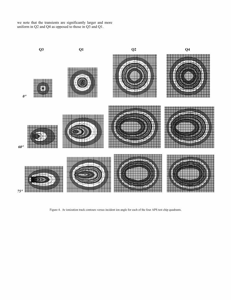
we note that the transients are significantly larger and more uniform in Q2 and Q4 as opposed to those in Q3 and Q1.
Q3 Q1 Q2 Q4
0°
60°
75°
Figure 4. Ar ionization track contours versus incident ion angle for each of the four APS test chip quadrants.

1 9
17 25 33 41 49 57 65 73 81 89 97
105
113
121
S1S23
S45S67
S89
S111
0100200300400500600700800900
100011001200130014001500
1600
1700
1800
DN
X
Y
1 9
17 25 33 41 49 57 65 73 81 89 97
105
113
121
S1S22
S43S64
S85
S106
S127
0100200300400500600700800900100011001200
1300
1400
1500
1600
1700
1800
DN
X
Y
1 917 25 33 41 49 57 65 73 81 89 97
105
113
121
S1S23
S45S67
S89
S111
0100200300400500600700800900
100011001200130014001500
1600
1700
1800
DN
X
Y
1 917 25 33 41 49 57 65 73 81 89 97
105
113
121
S1S23
S45S67
S89
S111
0100200300400500600700800900
100011001200130014001500160017001800
DN
X
Y
Figure 5. Typical data frames for each of the test chip quadrants provide a comparison of 60° incident Ar ionization strike signatures.
Q3 Q1
Q2 Q4

VI. CHARGE COLLECTION MODELING A sensor array charge transport model [4,5] is also under
development, and has been applied to the APS heavy ion data as well as to other sensor technologies as described in [5]. The current model accounts for charge collection by drift in high-field regions, such as depletion, and by diffusion in free-field regions. In Fig. 11, we show data for a normally incident Ar hit to Q1 on the left and Q2 in the middle. The simulation is shown on the right, with artificial saturation imposed at 1700 DN to normalize to the data. The simulation assumed a 1 µm depletion layer and 25 µm diffusion layer, with both layers covering the entire pixel area. In both the data plots and the simulation plot, the ion hit is in the center of the 11x11 array at normal incidence.
The simulation results are intermediate between the Q1 and Q2 data. We see general agreement on the gross characteristics of the charge spread. Q1 has a more focused charge collection and Q2 has a less focused charge collection than the simulation. The actual charge collection volumes within the pixel are much more complex than the simple depletion layer on a diffusion layer that is assumed for the simulation, and the electric fields within the structure probably modify the diffusion characteristics beyond the simple free-field diffusion assumed in this simulation. The intent of this analysis is to reproduce the gross features of the data. A more detailed analysis that takes the detailed pixel charge collection structures into account will be performed in the future, and promises to aid in the interpretation of the present data set.
VII. CONCLUSIONS Significant differences have been found in the transient
ionization response of the four quadrants of the Photobit APS test chip. Quadrant 3 is least sensitive to charge contamination from heavy ions whereas Ar hits in Q2 and Q4 cause saturation of the pixels at the point of impact and charge spread perturbs hundreds of pixels surrounding the ion track. The results suggest that the sensitivity to ion strikes is minimized by utilization of a non N-well, n+ recessed implant photodetector design. In addition, we observed no latch-up for a maximum LET of 106 MeV/mg/cm2 up to a fluence of
>2 x 107 cm-2. This result and the demonstration in [1] of total ionizing dose hardness to a level of 30 Mrad(Si), indicate that hardening by design in a commercial foundry is a viable approach to achieving APS sensor arrays with superior radiation performance in the space environment.
Finally, the degree of statistical variability in the numbers of disturbed pixels between individual ion strikes and the total signal charge collected is dependent on the pixel design. The uniformity is significantly greater for those pixels with a total signal charge dominated by substrate diffusion. Unfortunately, the area of disturbed pixels is also about ten times larger and the total collected signal charge much greater for these pixels, which demonstrates the importance of design techniques to minimize charge collection from substrate diffusion.
ACKNOWLEDGMENTS Eric Fossum of Micron generously provided detailed
processing information for the APS devices studied. We also thank Robert Spagnuolo from NASA-GSFC for providing the APS test chips from a NASA SBIR Phase II program.
REFERENCES
[1] El-Sayed Eid, T. Y. Chan, E.R. Fossum, R.H. Tsai, R. Spagnuolo, J. Deily, W.B. Byers, Jr., and J.C. Peden, “Design and characterization of ionizing radiation-tolerant CMOS APS image sensors up to 30 Mrd(Si) total dose,” IEEE Trans. Nucl. Sci., Vol. 48, pp. 1796-1806, Dec. 2001.
[2] E.R. Fossum, “CMOS image sensors: electronic camera-on-a-chip,” IEEE Trans. El. Dev., Vol. 44, pp. 1680-1698, Oct. 1997.
[3] G.R. Hopkinson, “Radiation effects in a CMOS active pixel sensor,” IEEE Trans. Nucl. Sci., Vol. 47, pp. 2480-2484, Dec. 2000.
[4] J.C. Pickel, R. Reed, R. Ladbury, B. Rauscher, P. Marshall, T. Jordan, B. Fodness and G. Gee, “Modeling radiation-induced transients in the Next Generation Space Telescope (NGST),” presentation at the 2002 IEEE Aerospace Conference, Big Sky MT, March 2002.
[5] J.C. Pickel, R. Reed, R. Ladbury, B. Rauscher, P. Marshall, T. Jordan, B. Fodness and G. Gee, “Radiation-induced collection charge in infrared arrays,” to be presented at the 2002 IEEE NSREC, Phoenix, AZ, July 2002.
Fig. 11. Ar ion hits at 0 degrees on quadrant 1 and 2 of the APS test chip compared to a model simulation.
1 3 5 7 9
11
S1
S5
S9
010020030040050060070080090010001100120013001400150016001700
1 2 3 4 5 6 7 8 9 10 11S1
S5
S9
0100200300400500600700800900100011001200130014001500160017001800
1 2 3 4 5 6 7 8 9 10 11S1
S5
S9
0100200300400500600700800900100011001200130014001500160017001800
Quad 1 Data, 0 Deg Quad 2 Data, 0 Deg Simulation, 0 Deg