hardware-software co-design, acceleration and prototyping
TRANSCRIPT
UNLV Theses, Dissertations, Professional Papers, and Capstones
12-1-2012
Hardware-Software Co-Design, Acceleration and Prototyping of Hardware-Software Co-Design, Acceleration and Prototyping of
Control Algorithms on Reconfigurable Platforms Control Algorithms on Reconfigurable Platforms
Desta Kumsa Edosa University of Nevada, Las Vegas
Follow this and additional works at: https://digitalscholarship.unlv.edu/thesesdissertations
Part of the Hardware Systems Commons, Software Engineering Commons, and the Theory and
Algorithms Commons
Repository Citation Repository Citation Edosa, Desta Kumsa, "Hardware-Software Co-Design, Acceleration and Prototyping of Control Algorithms on Reconfigurable Platforms" (2012). UNLV Theses, Dissertations, Professional Papers, and Capstones. 1728. http://dx.doi.org/10.34917/4332709
This Thesis is protected by copyright and/or related rights. It has been brought to you by Digital Scholarship@UNLV with permission from the rights-holder(s). You are free to use this Thesis in any way that is permitted by the copyright and related rights legislation that applies to your use. For other uses you need to obtain permission from the rights-holder(s) directly, unless additional rights are indicated by a Creative Commons license in the record and/or on the work itself. This Thesis has been accepted for inclusion in UNLV Theses, Dissertations, Professional Papers, and Capstones by an authorized administrator of Digital Scholarship@UNLV. For more information, please contact [email protected].

HARDWARE-SOFTWARE CO-DESIGN, ACCELERATION AND PROTOTYPING
OF CONTROL ALGORITHMS ON RECONFIGURABLE PLATFORMS
By
Desta Kumsa Edosa
Bachelor of Science in Electrical Engineering
Bahir Dar University, Ethiopia
June 2007
A thesis submitted in partial fulfillment of
the requirements for the
Master of Science in Electrical Engineering
Department of Electrical and Computer Engineering
Howard R. Hughes College of Engineering
The Graduate College
University of Nevada, Las Vegas
December 2012

ii
THE GRADUATE COLLEGE
We recommend the thesis prepared under our supervision by
Desta Kumsa Edosa
entitled
Hardware-Software Co-Design, Acceleration and Prototyping of Control Algorithms on
Reconfigurable Platforms
be accepted in partial fulfillment of the requirements for the degree of
Master of Science in Electrical Engineering Department of Electrical and Computer Engineering
Venkatesan Muhtukumar, Ph.D., Committee Chair
Emma Regentova, Ph.D., Committee Member
Sahjendra Singh, Ph.D., Committee Member
Ajoy K. Datta, Ph.D., Graduate College Representative
Tom Piechota, Ph.D., Interim Vice President for Research &
Dean of the Graduate College
December 2012

iii
ABSTRACT
HARDWARE-SOFTWARE CO-DESIGN, ACCELERATION AND
PROTOTYPING OF CONTROL ALGORITHMS ON RECONFIGURABLE
PLATFORMS
by
Desta Kumsa Edosa
Dr. Venkatesan Muthukumar, Examination Committee Chair
Associate Professor, Electrical and Computer Engineering,
University of Nevada, Las Vegas
Differential equations play a significant role in many disciplines of science and
engineering. Solving and implementing Ordinary Differential Equations (ODEs) and
partial Differential Equations (PDEs) effectively are very essential as most complex
dynamic systems are modeled based on these equations. High Performance Computing
(HPC) methodologies are required to compute and implement complex and data intensive
applications modeled by differential equations at higher speed. There are, however, some
challenges and limitations in implementing dynamic system, modeled by non-linear
ordinary differential equations, on digital hardware. Modeling an integrator involves data
approximation which results in accuracy error if data values are not considered properly.
Accuracy and precision are dependent on the data types defined for each block of a
system and subsystems. Also, digital hardware mostly works on fixed point data which
leads to some data approximations. Using Field Programmable Gate Array (FPGA), it is
possible to solve ordinary differential equations (ODE) at high speed. FPGA also
provides scalable, flexible and reconfigurable features.
The goal of this thesis is to explore and compare implementation of control
algorithms on reconfigurable logic. This thesis focuses on implementing control
algorithms modeled by second and fourth order PDEs and ODEs using Xilinx System

iv
Generator (XSG) and LabVIEW FPGA module synthesis tools. Xilinx System Generator
for DSP allows integration of legacy HDL code, embedded IP cores, MATLAB
functions, and hardware components targeted for Xilinx FPGAs to create complete
system models that can be simulated and synthesized within the Simulink environment.
The National Instruments (NI) LabVIEW FPGA Module extends LabVIEW graphical
development to Field-Programmable Gate Arrays (FPGAs) on NI Reconfigurable I/O
hardware. This thesis also focuses on efficient implementation and performance
comparison of these implementations. Optimization of area, latency and power has also
been explored during implementation and comparison results are discussed.

v
ACKNOWLEDGMENTS
I would like to express my sincere and deepest heartily gratitude to my professor Dr.
Venkatesan Muthukumar whose remarkable mentorship and guidance has been with me
from the start to the end of this work. A plain "thank you" phrase is really too simple to
express his indispensable guidance throughout this thesis work. He has taught me
learning by being challenged and finding different approaches to solve problems. I am
really appreciative for his constant follow-ups and his valuable time.
I am also very thankful to my advisory committees and my professors, Drs. Sahjendar
Singh and Emma Regentova, who without reserve have helped me with material
resources and in explaining many concepts for this thesis. My special thanks also go to
Dr. Ajoy Datta for being my Graduate College Representative.
My dearest wife, Lattuu, deserves special thanks first for loving me and determined to
be my wife forever and second for being an excellent young mom by taking great
responsibility in caring for our twin sons when situations have been challenging to her;
tolerating the pain of loneliness but yet encouraged me to go forward in my education.
I am very thankful to my parents, Obbo Kumsaa Iddoosaa and Aadde Baqqalee
Gaja'aa, for without their persistent commitment and sacrifice my being here could have
been unimaginable. They showed me their unbiased love, taught me what perseverance
mean, gave me the chance that they themselves never had in their entire life. Now, I can
see the world broadly through the door they opened for me. Thank you, Mom and Dad!
Lastly, but not least, I am grateful to all my brothers, sisters, relatives and friends
who stood beside me with their moral support until the end of this thesis.
GALATA
Warra koo, Obbo Kumsaa Iddoosaa fi Aadde Baqqalee Gaja'aa, carraa barumsaa osoo
hin argatiin, abdii ifaa tokko fulduratti ilaaluun, anatti dhubbanii, tabba jireenyaa bu'anii
bahanii, bifa lama natti baasanii, natti daaranii,asiin nagaahaniif; Haadha manaa koo,
Lattuu, dhibee yaaddoo fi kophummaa obsaan dandeessee, daa’ima keenya lamaan faana
qophaa waliin rakkachaa, itti cinniinnattee guddisaarra haamilee isheen na duukee buute
jaabadhu naan jetteef; obbolaa/tii wan koo warra fakkeenyaa na fudhachuun isaanii itti
gaafatamummaa guddaa natti ta’ee akkan cimu na godheef; akkasumas hiriyyoota koo fi
firoottan koo warra haamilee fi gorsa isaaniin na duukaa turan maraaf galatni koo guddaa
dha.

vi
DEDICATION
This work is dedicated to
My sons
Obsineet and Obsinuun

vii
ABSTRACT……………………………………………………………………... iii
ACKNOWLEDGMENTS………………………………………………………... v
GALATA………………………………………………………………………… .v
DEDICATION…………………………………………………………………… vi
LIST OF TABLES……………………………………………………………... xiii
LIST OF FIGURES…………………………………………………………….. xiv
CHAPTER 1 INTRODUCTION…………………………………………………. 1
1.1 The need for High Performance Computing…………………………….. 1
1.2 Research Objectives……………………………………………………... 5
CHAPTER 2 BACKGROUND…………………………………………………... 9
2.1 Trends in High Performance Computing………………………………... 9
2.2 LabVIEW………………………………………………………………. 12
2.3 LabVIEW FPGA Module……………………………………………….14
2.4 LabVIEW Real-Time Module…………………………………………..16
2.5 LabVIEW Control Design and Simulation Module……………………. 17
2.6 MATLAB /Simulink…………………………………………………… 18
CHAPTER 3 METHODOLOGY……………………………………………….. 20
3.1. Software Simulation……………………………………………………. 22
3.2. Hardware-Software Co-Simulation…………………………………….. 23
3.2.1. HW-SW Co-Simulation in XSG……………………………………. 23
3.2.2. LabVIEW Real-Time HW/SW Co-Simulation……………………... 25

viii
3.2.3. LabVIEW FPGA Hardware Software Co-Simulation……………… 26
3.3. Hardware Implementation Emulation………………………………….. 27
3.4. Hardware-in-the-Loop (HIL) Simulation………………………………. 27
3.5. Hardware-in-the-Loop (HIL) Emulation………………………………..29
CHAPTER 4 APPLICATION………………………………………………….. 30
4.1. Inferior Olive Neuron………………………………………………….. 30
4.2. Mathematical Model for Inferior Olive Neuron………………………...31
4.3. Inferior Olive Neuron Synchronization…………………………………32
4.3.1. Synchronization of IONs Using Gain Feedback Controller…………33
4.3.2. Synchronization Using Filter Feedback Controller…………………. 35
4.4. ION Driven PID Controlled DC Motor…………………………………36
4.4.1. DC Motor…………………………………………………………… 36
4.4.2. PID Controller………………………………………………………. 39
4.5. Lorenz Chaos System…………………………………………………….. 40
4.5.1. Control of Lorenz Chaos System………………………………………. 41
CHAPTER 5 IMPLEMENTATION……………………………………………. 42
5.1. Introduction to FPGA…………………………………………………... 42
5.2. Hardware Platforms……………………………………………………. 44
5.2.1. Spartan-3A DSP 3400A…………………………………………….. 45
5.2.2. NI PXI-8106 Embedded Controller………………………………… 45
5.3. Software Platforms……………………………………………………... 47

ix
5.3.1. Xilinx System Generator (XSG)……………………………………. 47
5.3.2. LabVIEW FPGA Module……………………………………………49
5.4. Implementation Process………………………………………………... 49
5.5. Implementation of Single Inferior Olive Neuron (ION)……………….. 51
5.5.1. Single ION Simulation Model……………………………………….51
5.5.1.1. MATLAB /Simulink Model ......................................................... 51
5.5.1.2. LabVIEW Model .......................................................................... 52
5.5.1.3. LabVIEW Real-Time Model ........................................................ 54
5.5.2. ION HW-SW Co-Simulation……………………………………….. 55
5.5.2.1. MATLAB XSG HW-SW Co-Simulation .................................... 55
5.5.2.2. LabVIEW FPGA HW-SW Co-Simulation .................................. 57
5.5.2.3. Development Flow in LabVIEW FPGA ...................................... 59
5.5.3. Hardware-in-Loop (HIL) Simulation………………………………. 62
5.5.3.1. Implementation of PID Controller ............................................... 63
5.5.3.2. Implementations of DC Motor ..................................................... 63
5.5.4. Hardware-in-the-Loop (HIL) Emulation…………………………… 70
5.5.4.1. HIL Emulation Implementation in LabVIEW FPGA .................. 71
5.5.4.2. HIL Emulation Implementation in XSG ...................................... 72
5.5.5. Hardware Emulation…………………………………………………74
5.6. Implementation of Synchronizations of IONs…………………………. 74
5.6.1. Implementation Synchronizations of Two IONs Using Gain Controller
………………………………………………………………………. 74
5.6.1.1. Simulation .................................................................................... 74

x
5.6.1.1.1. MATALAB/Simulink Simulation.......................................... 74
5.6.1.1.2. LabVIEW Simulation ............................................................ 75
5.6.1.1.3. LabVIEW Real-Time Simulation .......................................... 77
5.6.1.2. Hardware-Software Co-Simulation .............................................. 77
5.6.1.2.1. Using MATLAB XSG ........................................................... 78
5.6.1.2.2. Using LabVIEW FPGA ......................................................... 79
5.6.1.3. HIL Simulation ............................................................................. 81
5.6.1.3.1. Using MATLAB and XSG .................................................... 81
5.6.1.3.2. Using LabVIEW and LabVIEW FPGA ................................. 82
5.6.1.4. HIL Emulation.............................................................................. 83
5.6.1.4.1. Using XSG ............................................................................. 83
5.6.2. Synchronizations of Two IONs Using Filter Feedback Controller…. 84
5.6.2.1. HW-SW Co-Simulation ............................................................... 84
5.6.2.1.1. Using XSG ............................................................................. 84
5.6.2.2. HIL Emulation.............................................................................. 86
5.6.2.2.1. MATLAB XSG ...................................................................... 86
5.6.3. Implementation of Three IONs Synchronizations Using Gain Feedback
Controller…………………………………………………………….. 87
5.6.3.1. HW-SW Co-Simulation ............................................................... 87
5.6.3.2. HIL Emulation.............................................................................. 88
5.6.3.2.1. Using XSG ............................................................................. 88
5.6.4. Implementation of Three IONs Synch Using Filter Feedback Controller
………………………………………………………………………. 89
xi
5.6.4.1. HW-SW Co-Simulation using XSG ............................................. 89
5.6.5. Implementation of Three IONs Sync with Phase Shift Using Gain
Feedback Controller…………………………………………………. 90
5.6.5.2. HIL Emulation.............................................................................. 92
5.6.6. Implementation of Three IONs Synch with Phase Shift Filter Feedback
Controller…………………………………………………………….. 93
5.6.6.1. HW-SW Co-Simulation Using XSG ............................................ 93
5.7. Implementation of Lorenz Chaos System……………………………… 94
5.7.1. Simulation…………………………………………………………... 94
5.7.1.1. LCS using MATLAB-Simulink ................................................... 94
5.7.1.2. LCS Using LabVIEW .................................................................. 96
5.7.2. HW-SW Co-Simulation…………………………………………….. 97
5.7.2.1. Using XSG ................................................................................... 97
5.7.2.2. Using LabVIEW FPGA ............................................................... 98
5.8. Implementation Lorenz Chaos System Adaptive Controller…………... 99
CHAPTER 6 RESULTS………………………………………………………. 101
6.1. Hardware Resource Utilizations……………………………………… 101
6.2. Comparing Different Methodologies…………………………………. 104
CHAPTER 7 CONCLUSION AND FUTUREWORK………………………... 111
7.1. Conclusion……………………………………………………………. 111
7.2. Future Work…………………………………………………………... 112
REFERENCES………………………………………………………………… 113

xii
VITA…………………………………………………………………………… 119

xiii
LIST OF TABLES
Table 4.1 DC Motor Parameters ....................................................................................... 38
Table 5.1 Xilinx FPGA Comparison ............................................................................... 44
Table 5.2 Comparison of Different FPGA Families ......................................................... 47
Table 6.1 HW resource usage of ION and ION synchronization using filter feedback
controller on Spartan 3A DSP ................................................................................. 101
Table 6.2 HW resource usage of ION and ION synchronization using filter feedback
controller on Spartan Virtex-5 ML506 .................................................................... 102
Table 6.3 HW resource usage of ION and ION sync with gain feedback controller in . 102
Table 6.4 HW resource usage of ION and ION sync with gain feedback controller in
Virtex-5 ML506 ....................................................................................................... 102
Table 6.5 HW resource usage of ION and ION sync with gain controller using LabVIEW
FPGA ....................................................................................................................... 103
Table 6.6 HW resource usage of IONs and ION sync on Spartan 3E ............................ 103
Table 6.7 ION HIL device utilization ............................................................................. 104
Table 6.8 HW resource utilization comparison of LCS .................................................. 104
Table 6.9 ION and ION synch comparison for different methodologies with respect
simulation time ........................................................................................................ 105

xiv
LIST OF FIGURES
Figure 2.1 Components of LabVIEW. .............................................................................. 13
Figure 2.2 LabVIEW FPGA parallel processing ............................................................. 16
Figure 3.1 General block diagram of design methodology............................................... 21
Figure 3.2 HW implementation design flow in XSG ....................................................... 22
Figure 3.3 MATLAB-XSG HW-SW co-simulation design flow .................................... 24
Figure 3.4 LabVIEW RT HW-SW so-simulation design flow ......................................... 25
Figure 3.5 Hardware-in-the-loop block diagram using MATLAB-XSG ......................... 29
Figure 4.1 Synchronization of two IONS block diagram ................................................. 36
Figure 4.2 Circuit diagram of DC motor .......................................................................... 37
Figure 4.3 Block diagram of DC motor system ................................................................ 38
Figure 4.4 PID controller block diagram .......................................................................... 39
Figure 5.1 FPGA block diagram ....................................................................................... 43
Figure 5.2 Spartan-3A DSP 3400A block diagram .......................................................... 45
Figure 5.3 PXI-8106 block diagram ................................................................................. 46
Figure 5.4 Simple DSP implementation using XSG ......................................................... 50
Figure 5.5 Integrator implementation in XSG .................................................................. 51
Figure 5.6 Single ION model in Simulink ........................................................................ 51
Figure 5.7 ION Simulation result in Simulink. ................................................................ 52
Figure 5.8 Single ION model in LabVIEW ...................................................................... 53
Figure 5.9 ION simulation result in LabVIEW. ............................................................... 53
Figure 5.10 ION model in LabVIEW Real-Time. ........................................................... 54
Figure 5.11 ION Simulation result in LabVIEW Real-Time. .......................................... 55

xv
Figure 5.12 ION model in XSG ........................................................................................ 56
Figure 5.13 ION HW/SW co_simualtion result. .............................................................. 56
Figure 5.14 LabVIEW FPGA interactive front panel communication ............................. 57
Figure 5.15 Programmatic FPGA communication in LabVIEW FPGA/RT .................... 58
Figure 5.16 LabVIEW FPGA development flow ............................................................. 60
Figure 5.17 ION LabVIEW FPGA target VI .................................................................... 61
Figure 5.18 ION LabVIEW FPGA host VI ...................................................................... 61
Figure 5.19 ION HW/SW co-simulation result in LabVIEW FPGA. ............................. 62
Figure 5.20 PID model in XSG......................................................................................... 63
Figure 5.21 DC motor model in Simulink ........................................................................ 63
Figure 5.22 Step response of open loop DC motor in Simulink ....................................... 64
Figure 5.23 PID controlled DC motor model in Simulink................................................ 64
Figure 5.24 Step response of PID controlled closed loop DC motor in Simulink ............ 65
Figure 5.25 PID controlled DC motor model in LabVIEW.............................................. 65
Figure 5.26 Step response of PID controlled DC motor in LabVIEW ............................. 66
Figure 5.27 ION driven PID controlled DC motor model in LabVIEW .......................... 66
Figure 5.28 Simulation result of DC motor driven by IONs in LabVIEW....................... 67
Figure 5.29 Hardware model of PID controlled DC motor using XSG............................ 67
Figure 5.30 Hardware model of PID controlled DC motor using LabVIEW FPGA ........ 68
Figure 5.31 Hardware step response of PID controlled DC motor using XSG ................ 68
Figure 5.32 HIL simulation of IONS in MATLAB-XSG block Diagram ........................ 69
Figure 5.33 HIL simulation result of IONs using MATLAB-XSG. ................................. 70
Figure 5.34 HIL emulation model in LabVIEW FPGA ................................................... 71

xvi
Figure 5.35 HIL emulation result of IONs using LabVIEW FPGA ................................. 72
Figure 5.36 HIL emulation model using XSG .................................................................. 73
Figure 5.37 I/O signal comparison for ION HIL emulation in XSG ................................ 73
Figure 5.39 Two IONs synchronization model in MATLAB/Simulink ........................... 74
Figure 5.40 Two ION synchronization result with gain controller in Simulink. .............. 75
Figure 5.41 Two IONs synch with gain controller LabVIEW block diagram .................. 76
Figure 5.42 Two IONs sync with gain controller result in LabVIEW .............................. 76
Figure 5.43 Two IONs sync with gain controller result in LabVIEW RT ....................... 77
Figure 5.44 XSG model of two IONs sync with gain controller ...................................... 78
Figure 5.45 HW-SW co-sim result of two IONs sync using gain controller in XSG. ...... 79
Figure 5.46 LabVIEW FPGA model of HW-SW co-sim of two IONs with gain controller
................................................................................................................................... 80
Figure 5.47 HW-SW co-sim result of two IONs sync using gain controller in LabVIEW
................................................................................................................................... 80
Figure 5.48 Two IONs sync HIL simulation model with gain controller in MATLAB-
XSG ........................................................................................................................... 81
Figure 5.49 Two IONs sync with gain controller HIL simulation result in MATLAB-
XSG .......................................................................................................................... 82
Figure 5.50 Two IONs sync with gain controller HIL simulation result in LabVIEW-
LabVIEW FPGA ...................................................................................................... 83
Figure 5.51 Hardware model of filter feedback controller model in XSG ....................... 84
Figure 5.52 Two IONs sync with filter feedback controller in XSG ................................ 85
Figure 5.53 Two IONs sync with filter feedback controller in XSG ................................ 86

xvii
Figure 5.54 HIL emulation result of two ION synch with filter feedback controller in
XSG ........................................................................................................................... 87
Figure 5.55 HW-SW co-sim results of three sync IONs with gain feedback controller in
XSG .......................................................................................................................... 87
Figure 5.56 HIL emulation result of three ION sync with gain feedback controller in XSG
................................................................................................................................... 89
Figure 5. 57 HW-SW co-sim result of three IONs sync with filter feedback controller .. 90
Figure 5.58 Three IONs synch with phase shift and gain feedback controller model using
XSG ........................................................................................................................... 91
Figure 5.59 HW-SW co-sim of three phase shifted ION sync with gain feedback
controller ................................................................................................................... 92
Figure 5.60 Three ION sync with phase shift and filter feedback controller model in XSG
................................................................................................................................... 93
Figure 5.61 HW-SW co-sim of three phase shifted ION sync with filter feedback
controller in XSG....................................................................................................... 94
Figure 5.62 Lorenz chaos system model in Simulink ....................................................... 95
Figure 5.63 Lorenz chaos system model in MATLAB Simulink ..................................... 95
Figure 5.64 Simulation result of Lorenz chaos system in Simulink ................................. 96
Figure 5.65 Lorenz chaos system model in LabVIEW ..................................................... 96
Figure 5.66 Lorenz chaos system simulation result in LabVIEW .................................... 97
Figure 5.67 Lorenz chaos system model in XSG ............................................................. 97
Figure 5.68 Lorenz chaos system HW-SW co-sim result in XSG .................................... 98
Figure 5.69 Lorenz chaos system model (VI) using LabVIEW FPGA ............................ 98

xviii
Figure 5.70 Lorenz chaos system HW-SW so-sim result using LabVIEW FPGA .......... 99
Figure 5.71 XSG model of LCS controller ..................................................................... 100
Figure 5.72 LCS controller result. ................................................................................. 100

1
CHAPTER 1
INTRODUCTION
In this thesis Hardware-Software Co-design of different algorithms of control
application on reconfigurable devices are presented. The novelty of reconfigurable
hardware accelerators in the applications of High Performance Computing (HPC) field is
explored. Model based system designed has been done in software using MATLAB,
Simulink and National Instruments (NI) LabVIEW. These algorithms are implemented
on reconfigurable devices using Xilinx System Generator (XSG) and LabVIEW FPGA
tools on Xilinx Virtex and Spartan boards and NI Reconfigurable Input Output (RIO)
devices respectively.
1.1 The need for High Performance Computing
There is always a demand for processing data intensive application at higher speed.
Increase in size and complexity of application program, demands the use of High
Performance Computing (HPC) technologies to solve the problem efficiently and at
higher rate. The limitation on the efficiency of general purpose desktop computers to
process an application within a required time forces engineers and scientists to explore
custom and hardware accelerated methods.
Different definitions have been given for HPC by different authors. High
Performance Computing (HPC) is the use of parallel processing for running
advanced application programs efficiently, reliably and quickly [1]. It is stated in
[1][2][3][4] that originally HPC was used to describe systems that functions above

2
teraflops, floating point operation per second (TFLOPS). The term HPC is
occasionally used as a synonym for supercomputing [1], although technically a
supercomputer is a system that performs at or near the highest operational rate for
computers and the definition of HPC has evolved to include systems with any
combination of accelerated computing capacity, superior data throughput, and the ability
to aggregate substantial distributed computing power.
There are vast application areas of High Performance Computing (HPC). It is used in
different industries for different applications to perform specific computational and data-
intensive tasks which usually are too large or takes too long time to handle on ordinary
standard desktop computers to perform it at the required speed within the required time
limit [2]. Some of the industries that apply High Performance Computing (HPC) are [3]:-
Government labs: Climate modeling, nuclear waste simulation, warfare modeling,
disease modeling and research, and aircraft and spacecraft modeling.
Defense: Video, audio, and data mining and analysis for threat monitoring, pattern
matching, and image analysis for target recognition
Financial services: Options valuation and risk analysis of assets.
Geosciences and engineering: Seismic modeling and analysis, and reservoir
simulation.
Life sciences: Gene encoding and matching, and drug modeling and discovery.
Some scientific and technical applications are very demanding in terms of computational
intensity, size of data sets and number of I/O channels for online data streaming, analysis
and visualization. These applications require High Performance Computing (HPC)
computations in real-time constraints. This includes applications such as plasma control

3
in nuclear fusion, adaptive optics in extremely large telescopes, RF MIMO systems,
smart electrical grid control, high-resolution medical imaging, multi-agent distributed
robotic systems and large real-time Hardware-in-the-Loop simulations for complex and
dynamic systems, etc. [5].
Different trends have been seen in the implementation of High Performance
Computing (HPC) systems. Before the invention of multi-core systems, general purpose
single-core CPU-based systems were the processing systems of choice for HPC
applications [2]. The performance of single-core CPU based system increases with
frequency. Using single-core system for HPC by increasing its processor’s frequency has
already reached its limitation as increasing the frequency of the process results in higher
and performance saturation. Single core CPU’s physical limitation for high performance
computing is a stimulus for the invention of multi-core architecture to meet high
performance demand. The shift to multicore CPUs forces application developers to adopt
a parallel programming model to exploit CPU performance [2]. In the 90’s, Symmetric
Multiprocessing (SMP) and Massively Parallel Processing (MPP) systems were the most
common architectures for high performance computing [3]. With the emergence of
effective cluster computing, the popularity of SMP and MPP has diminished [6].
Applications that are a good fit for the cluster architecture are those that can be
“parallelized,” or broken into sections that can be independently handled by one or more
program threads running in parallel on multiple processors. Such applications are
widespread, appearing in industries such as finance, engineering, bio-informatics, and oil
and gas exploration [3]. Clusters are becoming the preferred HPC architecture because of
their cost effectiveness. However, these systems have many challenges. The single-core

4
processors used in these systems are becoming denser and faster, but they are running
into memory bottlenecks and dissipating ever-increasing amounts of power [3].
Grid computing is now becoming popular as an alternative to HPC. Grid computing is the
technology for coordinated utilization of vast amounts of distributed compute resources
for virtual supercomputing. The grid computing can be utilized not only to connect
supercomputers but also to enable virtual TERA-scale computing powers to be obtained
by combining smaller-scale cluster systems [7].
For users that are running the most data- and computational- intensive applications,
the high performance growth they demand may not be delivered even using the newest
multicore architecture [4]. To satisfy this greedy and unlimited human needs, integrated
CPU-based systems augmented with hardware accelerators as co-processors such as
Graphics Processing Units (GPU) and FPGA, and other accelerator technologies can be
used to achieve the high performance efficiency to a stage that never been attained
before.
FPGAs typically run at much slower clock speeds than the latest CPUs, yet they can
more than make up for this with their superior memory bandwidth, high degree of
parallelization, and the customization. An FPGA coprocessor programmed to hardware-
execute key application tasks can typically provide a 2X to 3X system performance boost
while simultaneously reducing power requirements 40% as compared to adding a second
processor or even a second core. Fine tuning of the FPGA to the application’s needs can
achieve performance increases greater than 10X [3].
Some data intensive applications such as large real-time Hardware-in-the-Loop
simulations for complex dynamic systems, smart electrical grid control, Signal and

5
Communication Intelligence [5][8] need High Performance Computing (HPC) under
Real-Time constraints. This application can be implemented using multicores running
real-time operating system (RTOS), Field Programmable Gate Array (FPGA), access to
NVIDA graphic processing unit (GPU) through CUDA and CUBLAS toolkits and
libraries and using high speed mixed signal acquisition and generations NI modular
hardware using LabVIEW Real-Time.
1.2 Research Objectives
This thesis focuses on implementing control algorithms containing second and fourth
order Partial Differential Equations (PDEs) and Ordinary Differential Equations (ODEs)
using Xilinx System Generator (XSG) and LabVIEW FPGA module tools. Xilinx System
Generator for DSP allows integration of legacy HDL code, embedded IP Cores,
MATLAB functions, and hardware components targeted for Xilinx FPGAs to create
complete system models that can be simulated within the Simulink environment. The NI
LabVIEW FPGA Module extends LabVIEW graphical development to Field
Programmable Gate Arrays (FPGAs) on NI Reconfigurable I/O hardware.
This thesis also focuses on efficient implementation and performance comparison of
these implementations. Optimization of area, latency and power has been explored during
implementation and comparison results are discussed.
In this thesis, custom embedded hardware accelerator such as Xilinx’s Field
Programmable Gate Arrays (FPGA), NI PXI-8106 embedded controller and NI
Reconfigurable I/O (RIO) device (NI PXI-7811R), has been used to accelerate
application development. Xilinx System Generator (XSG), Matlab/Simulink, LabVIEW,

6
LabVIEW FPGA Module, LabVIEW Real-time module and LabVIEW Control Design
and Simulation tools have been used to develop and implement the algorithms.
Advancements in silicon, software, and IP Cores have proven that Xilinx FPGAs to
be the ideal solution for accelerating applications on high-performance embedded
computers and servers [2]. On the other hand, the parallelism (data parallelism, task
parallelism) and pipelining features of LabVIEW allows maximizing efficiency in high
performance computing. In addition, LabVIEW has different interfaces or modules to aid
high performance computation and hardware accelerators. For example, VI server for
grid computing, parallel loops (for loops) for multicore, CUDA interface to LabVIEW for
GPU, LabVIEW FPGA module for FPGA, and LabVIEW Real-Rime for real-time
systems. Algorithms in this thesis have been implemented on hardware targeting for
Virtex-II on NI PXI-7811R device using LabVIEW FPGA and on Spartan 3A Xtreme
DSP and Virtex-5 boards using Xilinx system generator (XSG). Hardware-in-the-Loop
(HIL) and Hardware-Software Co-simulations have done for verification of the design.
Hardware-in-the-Loop (HIL) simulation is a technique used by designers and test
engineers to validate and verify system components during design of a new system or
new component of a system.
Hardware-in-the-Loop (HIL) simulation is a technique that is used in the
development and test of complex real-time embedded systems [4]. HIL simulations
involve simulating some part or a component of a system under real-time environment or
using simulation model of the plant. Xilinx system Generator (XSG) provides for the
hardware simulation and Hardware-in-the-Loop (HIL) verification, referred to as
hardware co-simulation, within Simulink environment [9]. It’s easier to use Xilinx

7
System Generator (XSG) for hardware implementation and verification than using the
more complex Hardware Description Language (HDL) programming.
Different implementation methodologies have been involved in this thesis. Software
simulations, hardware simulations and implementations, Hardware-Software co-
simulations, Hardware-in-the-Loop (HIL) simulations and Hardware-in-the-Loop (HIL)
emulations have been used. Based on the device utilization and latency, performance
comparison has been done between LabVIEW FPGA implementation and Xilinx System
Generator implementations.
The control algorithms targeted in this work include: Inferior Olive Neurons (IONs),
Inferior Olive Neurons synchronizations using gain and filter feedback controllers,
Lorenz Chaos Systems (LCS) and Lorenz Chaos System control using L1 adaptive
controller.
The structure of this thesis is divided into seven chapters. Chapter 2 presents High
Performance Computing (HPC) background and its trend. It also briefly discusses the
tools used for the implementations of algorithms. Chapter 3 explains the methodology
followed for the implementations and verifications of algorithms used in this thesis.
Chapter 4 elaborates the applications this thesis is focused on and their mathematical
models. Chapter 5 discusses the hardware and software implementations of different
algorithms used in this thesis. Implementations have been done and results were
discussed in this chapter. Chapter 6 compares and explains the results of algorithms
implemented with respect to the hardware resource utilizations and latency. Performance
comparison between implementations using XSG and LabVIEW has also been made.

8
Chapter 7 concludes and summarizes what has been done in this thesis. Future work and
recommendation were also made.

9
CHAPTER 2
BACKGROUND
In this chapter, current trends of High Performance Computing (HPC) and its
applications have been discussed. The tools used for the implementations of HPC on
hardware accelerators have also been explained in this chapter. In this thesis, Xilinx
System Generator (XSG) and NI LabVIEW FPGA are tools used to design applications
for hardware implementations. Both tools provide parallel programming and
synthesizable blocksets which can be directly translated into logic blocks and
implemented on reconfigurable logic devices. The data types of functional blocksets are
configured manually so as to give the required data precision. Different LabVIEW add-
on modules, used in this thesis, have also been discussed in this section. LabVIEW FPGA
modules, Control Design and Simulation module, and LabVIEW Real-Time modules are
the three main modules used for the implementation of applications in this thesis.
2.1 Trends in High Performance Computing
It is stated that the introduction of vector computer systems marked the beginning for
modern supercomputing. A vector computer or vector processor [3] is a machine
designed to efficiently handle arithmetic operations on elements of arrays, called vectors.
Using single-core system for HPC by increasing its processor’s frequency has already
reached its limitation as increasing the frequency of the process results in high energy
consumption and brings CPU’s heat dissipation to impractical physical limit. As
computational power can no longer be efficiently increased through the addition of
transistors thereby increasing the frequency of the processor, the end of Moore’s Law,

10
drastic efforts have been made to improve computational tools using other means [10].
Single core CPU’s physical limitation for high performance computing is a stimulus for
the invention of multi-core architecture to meet high performance demand. The shift to
multicore CPUs forces application developers to adopt a parallel programming model to
exploit CPU performance [2].
There are different hardware architectures which support these parallel tasks with
multiplicity of hardware [11].
Superscalar Processors are single processors able to execute concurrently more
than one instruction per clock cycle.
Vector processors are processors designed to optimize the execution of arithmetic
operation in long vectors. These processors are mostly based on the pipeline
architecture.
Shared memory multiprocessors, symmetrical multi-processing (SMP) are
machines composed of processors which communicate among themselves through
a global memory shared by all processors.
SIMD (Single Instruction stream, Multiple Data stream) massively parallel
machine are composed of hundreds of thousands of relatively simple processors
which execute synchronously the same instruction on different sets of data (data
parallelism) under a command of central command unit.
Distributed Memory multicomputer are machines composed of several pairs of
memory-processor sets, connected by a high speed data communication network
which exchanges information through message passing.

11
Heterogeneous Network of workstations may be used as a virtual parallel machine
to solve a problem concurrently by the use of specially developed communication
and coordination software like PVM (parallel Virtual machine) and MPI (message
passing interface).
Although, performance of HPC systems are drastically changing every time, for
example, as it is explained in [12], the performance of HPC systems increased by 1000
factors within 11 years from Gigaflops (Cray2 in 1986), via Teraflops (Intel ASCI Red in
1997) up to the Petaflops (IBM Roadrunner in 2008), high computer intensive application
are still requiring faster system than what exists today.
The demand for higher speed HPC are coming from a variety of areas [12], involving
quantum mechanical physics, weather forecasting, climate research, molecular modeling
(computing the structures and properties of chemical compounds, biological
macromolecules, polymers, and crystals), physical simulations (such as simulation of
airplanes in wind tunnels and research into nuclear fusion), cryptanalysis, and improved
seismic processing for oil exploration for continued supply. For most of these
applications detailed results may only be achieved with systems in the Petaflops range.
To satisfy this demand, the current trend of HPC is [2] toward using multi-core
systems with large clusters with parallel reconfigurable computing; using processors
with add-on heterogeneous reconfigurable hardware accelerators such as FPGA,
Graphic Processing Unit (GPU), and cloud computing. Integrating reconfigurable
computing with high performance computing, exploiting reconfigurable hardware with
their advantages to make up for the inadequacy of the existing high-performance
computers had gradually become the high performance computing solutions and trends

12
[13]. The major challenges to all processor requirements for HPC systems now and in the
future will be [12], though: low cost, low power consumption, availability of support for
parallel programming, and efficient porting of existing codes.
In this thesis, software development tools which provide rapid prototyping of
algorithms on reconfigurable devices have been used. Software tools used in this thesis
are, MATLAB2010a with Simulink from Mathworks, System Generator 13.4 for DSP
and ISE 13.4 from Xilinx, LabVIEW, LabVIEW FPGA, LabVIEW Real-Time and
LabVIEW Control Design and Simulation from National Instruments (NI). Although the
Xilinx ISE 13.4 [13] foundation software is not directly utilized, it is required due to the
fact that it is running in the background when the System Generator blocks are
implemented. The following subsequent sections explains briefly the tools used.
2.2 LabVIEW
LabVIEW (Laboratory Virtual Instrumentation Engineering Workbench), from
National Instruments (NI), is one of the software platforms used to implement application
on hardware in this work. LabVIEW [14] is a graphical based program development
environment that uses icons instead of lines of text to create applications. Because of the
similarity of LabVIEW icons and physical instruments in appearance and its mimicry of
physical instruments’ operations such as oscilloscopes, multimeters, temperature gauge
and thermometer, LabVIEW programs are called virtual instruments, or VIs. Virtual
instrument's (VI’s) high level of abstraction and being graphical based programming
make LabVIEW programming more user friendly and easier to program than text based
programs. In contrast to text-based programming languages, where instructions
determine program execution, LabVIEW uses dataflow programming, where the flow of

13
data determines execution [14]. There are three main components of VI as shown in
Figure 2.1.Front panel (serves as the user interface), block diagram (contains the
graphical source code that defines the functionality of the VI) and Icon and connector
pane (identifies the VI so that you can use the VI in another VI).
Figure 2.1 Components of LabVIEW. a) front panel b) block diagram c) icon d) connector pane
LabVIEW is system design software that is used by engineers and scientists to
efficiently design, prototype, and deploy, data acquisition, embedded monitoring and
control applications [15]. Its being high level of abstraction language, which combines
hundreds of prewritten libraries, tight integration and interface with varieties of off-the-
shelf hardware, and a variety of programming approaches including graphical
development, .m file scripts, and connectivity to existing, C and HDL code and code
reusability make it ideal for development to deployment time short.

14
LabVIEW is a modular package containing add-ons software from NI and third party
partners. The flexibility and reconfigurability of prepackaged LabVIEW functions and
sophisticated tools allows designing specific application which meets one’s requirement.
There are different LabVIEW add-on modules used for design, prototype, and deploy
applications to hardware targets. In this thesis, Control Design and Simulation module,
LabVIEW FPGA module, LabVIEW Real-Time module have been used for simulating
our application on host machine and prototyping and deploying on the target devices. The
following sections discuss these modules in detail.
2.3 LabVIEW FPGA Module
Traditionally, FPGAs have been programmed using VHDL or Verilog. Many
engineers and scientists are either not familiar with these complex languages or require a
tool that gives them faster design productivity at a higher level of abstraction to greatly
simplify the process of generating Field Programmable Gate Array (FPGA) code.
LabVIEW FPGA is easier to get up and running than the alternative tools [16]. Since
LabVIEW programming involves parallelism and dataflow, it is well suited for FPGA
programming on NI reconfigurable I/O (RIO) hardware. LabVIEW’s graphical based
programming feature allows users, who have no much experience with VHDL
programming, to apply the FPGA design on reconfigurable devices.
On a CPU based target such as Windows the graphical code is scheduled into serial
program execution where all functions and operation are handled sequentially on the
processor. The LabVIEW scheduler takes care of managing multiple loops, timing,
priorities and other settings that determine when each function is executed. This
sequential operation causes timing interaction between different parts of an application

15
and creates jitter in program [17]. On an FPGA-based target, each application process
(subset of the application defined) is implemented within a loop structure. The LabVIEW
diagram is mapped to the FPGA gates and slices so that parallel loops in the block
diagram are implemented on different sections of the FPGA fabric. This allows all
processes to run simultaneously (in parallel) [17]. The timing of each process is
independent of the rest of the diagram, which eliminates jitter. This also means that you
can add additional loops without affecting the performance of previously-implemented
processes. You can add operations that enable interaction between loops for
synchronization or exchanging data. Data between parallel loops can also be exchanged
by using shared variables or FIFOs. FIFOs are also used to buffer data and pass it
between two data dependent loops or from host to target and vice versa.
For example, a typical data acquisition (DAQ) application can be partitioned into
processes for data acquisition, data processing, and data transfer to a host application as
shown in Figure 2.2.

16
Figure 2.2 LabVIEW FPGA parallel processing [17]
Mathematical model of algorithms implemented in this thesis involves non-linear
differential equations. An integrator is required to implement these equations on
hardware. A customized integrator has been modeled and implemented in LabVIEW
FPGA module from its approximated mathematical model . As
this approximation results in some computational error, taking proper values of dt is very
important in order to get optimal precision.
2.4 LabVIEW Real-Time Module
In some applications large and data extensive computation need to be done in real-
time. Real-Time processing doesn’t necessarily mean real fast [18] but processing the

17
application within deterministic and predictable time. Many HPC applications perform
offline simulations thousands and thousands of times and then report the results. This is
not a real-time operation because there is no timing constraint specifying how quickly the
results must be returned. The results just need to be calculated as fast as possible [18, 19].
Real-time applications have algorithms that need to be accelerated but often involve the
control of real-world physical systems– so the traditional HPC approach is not applicable.
In a real-time scenario the result of an operation must be returned in a predictable amount
of time. Engineers and scientists are now able to address a new domain of problem-
solving based on “Real-Time Numerical Analysis” using a high-performance computing
(HPC) approach with off-the-shelf hardware. The invention of multicores processors and
real-time OS technologies that utilize symmetric multiprocessing (SMP) to allow for real-
time software to be load-balanced across multiple CPU cores facilitated the realization of
real-time high Performance computing.
Real-Time high performance computing (RT-HPC) can be implemented on
multicores using LabVIEW programming languages as LabVIEW allows parallel
programing such as pipelining, task parallelism and data parallelism.
2.5 LabVIEW Control Design and Simulation Module
There are two types of applications that take advantage of LabVIEW Control design
and Simulation Module [20], rapid control prototyping (RCP) and hardware in the loop
(HIL). The main purpose of RCP applications is to check algorithms developed during
the design/simulation phase and deploy them to a real-time system to quickly verify the
performance of the algorithm. In an HIL application, the goal is to simulate a plant to be
controlled with the same input/output and behavior so that the test can be performed

18
safely. RCP and HIL have been used for years in the automotive and aerospace markets,
but they are now expanding into new areas such as medical devices, oil and gas, and
robotics.
Code built in LabVIEW Control Design and Simulation module can directly be
deployed to real target. In this thesis, control applications have been designed and run on
NI PXI 8106 controller running Real-Time OS.
2.6 MATLAB /Simulink
MATLAB/Simulink from Mathworks is another software platform we used for the
analysis and implementations of algorithms. MATLAB [22] is a high-level language and
interactive environment for numerical computation, visualization, and programming.
Using MATLAB, one can analyze data, develop algorithms, and create models and
applications.
MATLAB can be used for a range of applications, including signal processing and
communications, image and video processing, control systems, test and measurement,
computational finance, and computational biology. For the hardware translation of our
model from MATLAB /Simulink, we used Xilinx System Generator (XSG) tool which is
MATLAB based tools used for design and prototyping algorithms on reconfigurable
logics.
In this thesis, different algorithms are modeled both in LabVIEW and MATLAB
then translated into hardware using synthesizable blocksets in LabVIEW FPGA and
Xilinx System Generator (XSG). High level of abstraction in LabVIEW FPGA and XSG
tools facilitates application development within short period of time without the expert
knowledge of VHDL language. It is this feature that motivated us to use these tools to

19
implement algorithms on hardware. Verification of algorithms' implementation has been
done using software-hardware Co-simulations, HIL simulation and HIL emulations. The
designs have been evaluated based on latency and areas-resources utilizations. XSG DSP
blocks and LabVIEW FPGA supports only fixed point numbers. To get good precision of
the result, it is necessary to define the number of data bits and data types of each DSP
blocks manually so that it includes numerical ranges of the required data. If data type and
number of bits is not appropriately assigned to each blocksets, a computational error
could happen due to data quantization and overflow.

20
CHAPTER 3
METHODOLOGY
In this chapter, the methodologies and approaches used for the implementation of
each algorithm are explained. Different methodologies have been chosen to implement
the algorithms; Software Simulation, Hardware Emulation, Hardware-Software Co-
Simulation, Hardware-in-the-Loop (HIL) Simulation, Hardware-in-the-Loop (HIL)
Emulation. Figure 3.1 shows the general hardware and software design methodologies
that has been applied for the implementation of algorithms in this thesis.
Two particular approaches (tools) have been used for each application's
implementation, one is using MATLAB based Xilinx System Generator (XSG) and the
other approach is using NI LabVIEW and LabVIEW FPGA module. For each
application, from its mathematical model, first a Simulink and LabVIEW software model
is designed and simulated to analyze if the result meets the specification requirements.
After the simulation results met the expected requirements, the design was translated into
hardware using Xilinx System Generator (XSG) and LabVIEW FPGA module. The
hardware translated design was also simulated and the simulation results were compared
with pure software simulation results before synthesizing into hardware for final bit file
generation. When the Hardware and software simulation results matched, the hardware
translated design was compiled using Xilinx ISE and bitfile generated to be downloaded
to the FPGA. Some of the algorithms have also been implemented on NI PXI 8106 Real-
Time controller using LabVIEW Real-Time Modules.

21
Figure 3.1 General block diagram of design methodology
As shown in the Figure 3.1, different methodologies have been involved for
implementation of algorithms. The following sections discuss in detail about each
methodology. Figure 3.2 shows hardware implementation design flow of algorithms
using Xilinx System generator.

22
Figure 3.2 HW implementation design flow in XSG
3.1. Software Simulation
MATLAB /Simulink are used to design and model a system and analyze its
behavior. MATLAB is a high-level language and interactive environment for numerical
computation, visualization, and programming [21]. Using MATLAB, one can analyze
data, develop algorithms, and create models and applications. Simulink provides a
graphical editor, customizable block libraries, and solvers for modeling and simulating
dynamic systems [22]. It is integrated with MATLAB and enables to incorporate
MATLAB algorithms into models and export simulation results to MATLAB for further
analysis.
In addition to the MATLAB/Simulink, the systems have also been designed, simulated
and analyzed using LabVIEW and LabVIEW Real Time. LabVIEW Control Design and

23
Simulation module was used to develop application which runs on NI’s Real-Time
platform and windows PC. National Instruments created LabVIEW Real-Time to address
the need for deterministic real-time performance for applications that require
deterministic process that non-real-time operating systems like Windows cannot
guarantee. Some applications in this thesis have been designed using LabVIEW and
LabVIEW Control Design and Simulation Module and finally deployed directly (without
code generation) to real-time targets, PXI 8106 controller which run in Real-Time
Operating System (RTOS).
3.2. Hardware-Software Co-Simulation
3.2.1. HW-SW Co-Simulation in XSG
After the design specification of algorithms has been verified using MATLAB/
Simulink simulation, the design was translated into hardware using Xilinx system
Generator (XSG). System Generator [22] is a DSP design tool from Xilinx that enables
the use of The Mathworks model-based design environment Simulink for FPGA design.
The hardware model built using XSG was then simulated for functional verification using
Simulink environment taking the MATLAB/Simulink simulation result as test bench. If
the hardware functional simulation result matches that of the Simulink simulation results,
the model is ready to be transferred into Hardware. System generator is used to translate
the model into hardware. System clock rate and frequency is defined using system
generator token block. System Generator provides several methods to transform the
models built using Simulink into hardware. One of these methods is called Hardware-
Software Co-Simulation. Hardware-Software co-simulation enables building a hardware
version of the model and using the flexible simulation environment of Simulink. One can

24
also perform several tests to verify the functionality of the system in hardware. Xilinx
System Generator provides hardware co-simulation, making it possible to incorporate a
design running in an FPGA directly into a Simulink simulation. HW/SW Co-simulation
supports FPGAs from Xilinx on boards that support JTAG or Ethernet connectivity.
Several boards are predefined on System Generator for co-simulation. Even if a board is
not predefined in system generator, it is possible to define it. The HW/SW Co-Simulation
has been shown in Figure 3.3.
Figure 3.3 MATLAB-XSG HW-SW co-simulation design flow
Xilinx JTAG Hardware Co-Simulation block, which represents the whole hardware
model, is generated after synthesis using System Generator token if hardware Co-
Simulation is chosen as compilation option. The Xilinx JTAG Co-Simulation block
allows us to perform hardware Co-Simulation using JTAG.
The port interface of the Co-simulation block varies. When a model is implemented for
JTAG hardware co-simulation, a new library is created that contains a custom JTAG co-
25
simulation block with ports that match the gateway names, from the original model [23].
The co-simulation block interacts with the FPGA hardware platform during a Simulink
simulation. Simulation data that is written to the input ports of the block are passed to the
hardware by the block. Conversely, when data is read from the co-simulation block's
output ports, the block reads the appropriate values from the hardware and drives them on
the output ports so they can be interpreted in Simulink. In addition, the block
automatically opens, configures, steps, and closes the platform.
Procedure in XSG HW/SW Co-simulation
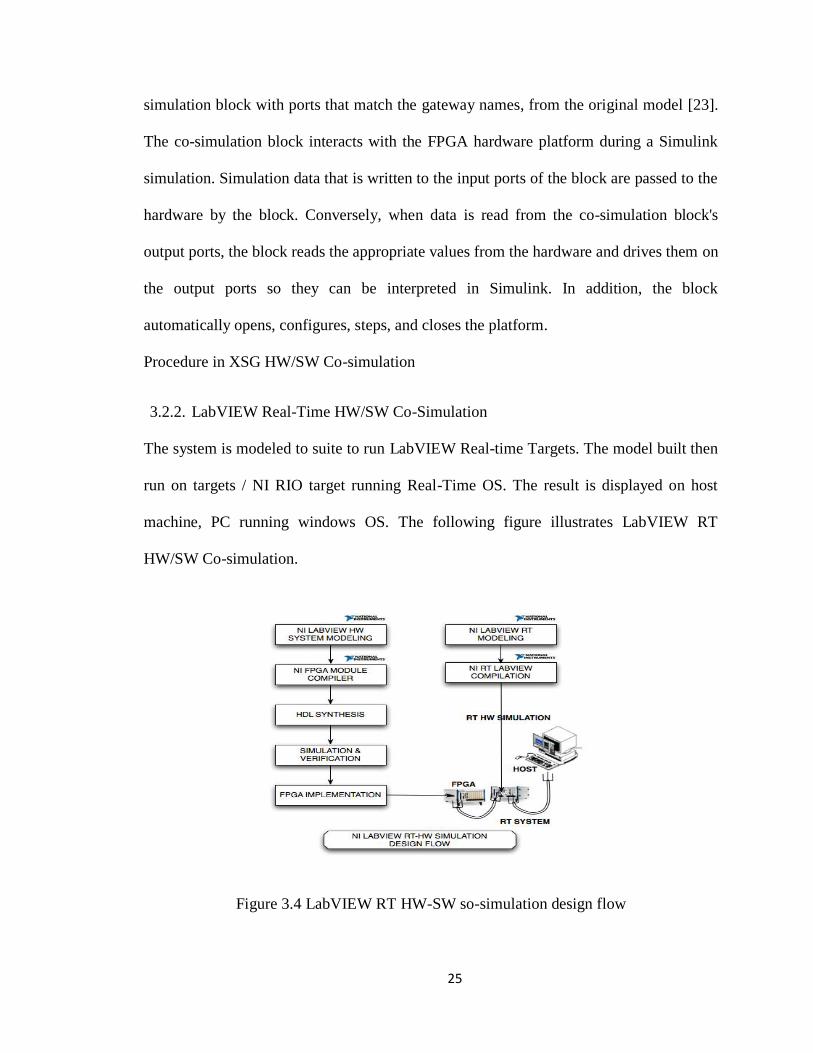
3.2.2. LabVIEW Real-Time HW/SW Co-Simulation
The system is modeled to suite to run LabVIEW Real-time Targets. The model built then
run on targets / NI RIO target running Real-Time OS. The result is displayed on host
machine, PC running windows OS. The following figure illustrates LabVIEW RT
HW/SW Co-simulation.
Figure 3.4 LabVIEW RT HW-SW so-simulation design flow

26
3.2.3. LabVIEW FPGA Hardware Software Co-Simulation
While LabVIEW programming for desktop PCs does not necessarily dictate a
structured development process, programming for FPGA targets without a proper design
flow can lead to significant inefficiency due to the long compilation times incurred
between algorithm design and test [24]. It is important to simulate the design for
behavioral verification before compiling it and waiting for long time and repeating the
same step until the design meet the required specification. Using proper simulation steps
before compilations can avoid the unnecessary time spent waiting for compilation. The
basic steps used for the implementation of algorithms in LabVIEW FPGA are [25]:
1. developing a behavioral model of the algorithm using LabVIEW and LabVIEW
Control Design and Simulation Module
2. Simulating for behavioral correctness of the algorithms designed in step 1 above
3. Creating structural IP for FPGA-based implementation,
4. Simulation of the structural IP on a desktop PC and check if matches with result
in 2. If so go to step 5 if not go to step 3
5. Compiling the IP for an FPGA, and finally testing of the design on FPGA.
Hardware testing was done using Hardware Co-simulation. It can also be done using
real world physical I/O. In Hardware Co-simulation the FPGA VI is compiled to the real
hardware target device and runs on it rather than simulating on host machine, desk top
PC. Once compiled to the target device, this simulation provides true cycle-accurate
simulation, and the simulation occurs at a much higher rate than simulating on host
machine. To transfer data between target VI and Host VIs DMA FIFO s have been used.

27
As compiling FPGA VI to the target device takes too long time, even days some times,
before final compilation is done it are recommended to simulate it on Host PC and
compare the results for functional verification. After the required result is obtained, it is
compiled to the target device for final download.
3.3. Hardware Implementation Emulation
In Hardware emulation approach, the whole system or component is implemented on
the hardware using XSG and LabVIEW FPGA module and the output results is analyzed.
The model that runs on Simulink environment is hardware Co-simulation blocksets
which imitates the behavior of the real FPGA as the results is being calculated in the
hardware and given out to the MATLAB workspace.
3.4. Hardware-in-the-Loop (HIL) Simulation
In the process of developing a new system, building a hardware prototype for the
whole system and testing the entire system will ask lots of energy, time and money. As
the system is getting bigger and more complex, the risks of trying to test the whole
system as a single entity could be many folds. Sometimes, it is required to design and test
one component of a system and test it. For example, an embedded controller for cars or
some bigger plant is needed to be designed and tested. It could be, however, impossible
to get the real plant every time we need to test our component or the real plant never
exists. During such limitation Hardware-in-Loop (HIL) came as a solution. Hardware-in-
the-Loop (HIL) simulation is achieving a highly realistic simulation of equipment in an
operational virtual environment [26]. HIL simulation provides an effective platform by
adding the complexity of the plant under control to the development and test platform.
The complexity of the plant under control is included in test and development by adding

28
a mathematical representation (model) of all related dynamic systems. These
mathematical representations are referred to as the "plant simulation."[27].
Unlike traditional testing, referred to as static testing [26], where functionality of a
particular component is tested by providing known inputs and measuring the outputs,
Hardware-in-the-loop (HIL) involves dynamic testing, where components are tested
while in use with the entire system, either real or simulated. Because of cost and safety
concerns, simulating the rest of the system with real-time hardware is preferred to testing
individual components in the actual real system. Testing a system component using the
simulation of a system or plant is known as Hardware-in-the-Loop (HIL) simulation.
In this thesis, a plant–PID controlled DC motor is implemented in hardware and
driven by IONs signals which are implemented in software using MATLAB Simulink
tool. The ION simulation results are stored in MATLAB workspace and accessed using
ROM blocksets from Xilinx System Generator (XSG) toolbox in Simulink library. As
shown in Figure, 3.5 below, the data stored in ROM are made to be accessed using free,
up running, counter which has the same size as data width of the ROM.

29
Figure 3.5 Hardware-in-the-loop block diagram using MATLAB-XSG
3.5. Hardware-in-the-Loop (HIL) Emulation
In the HIL emulation approach, Inferior Olive neurons, systems and controller are
implemented in hardware. The system/Plant used in this thesis is model of DC motor
controlled by PID controller. The PID controlled DC motor is made to be driven by ION
which is also in hardware ware. The whole system is implemented and emulation results
have been compared with other approaches. JTAG has been used for connecting to the
hardware and displaying the result back to the PC.
Using all these different approaches, output values have been compared and are the same.
The approaches discussed above will be applied to application areas explained in the next
chapter.

30
CHAPTER 4
APPLICATION
In this chapter, the application areas this thesis focused on have been discussed.
Mathematical model of the systems and algorithms implemented in this thesis has been
formulated and discussed in detail. Application area, this thesis centered on, is mainly
control application. Implementation of Inferior Olive Neuron (ION) and their
synchronization is the main focus of this thesis. Different controllers for ION
synchronization have been designed and implemented using XSG and LabVIEW FPGA.
Lorenz Chaos System (LCS) and adaptive Lorenz Chaos System (LCS) controller have
also been implemented on Field Programmable Gate Array (FPGA) hardware using XSG
and LabVIEW.
4.1. Inferior Olive Neuron
The olivo-cerebellar system is one of the important neuronal circuits in the brain. It
plays a key role in providing highly coordinated signals for the temporal organization of
movement execution [28]. Functionally, its network dynamics is organized around the
oscillatory membrane potential properties of inferior olive neurons (ION) and their
electronic connectivity [29]. The IONs have various features including subthreshold
activity in which the membrane potential has sustained fluctuations. The time varying
membrane potential can take a variety of shapes including sinusoidal, quasi-periodic,
regular spiking and irregular waveforms [1]. Inferior olive neurons (IONs) have rich
dynamics and can exhibit stable, unstable, periodic, and even chaotic trajectories. Inferior
olive neurons (IONs) are electrically coupled through gap junctions, generating

31
synchronous subthreshold oscillations of their membrane potential at a frequency of 1–10
Hz and are capable of fast and reliable phase [30].
A dynamic behavior of ION has been studied by many researchers and a
mathematical models ION, for capturing its electrophysiological properties observed in
laboratory tests, have been developed [28]. The dynamical properties of the ION depend
on the extracellular stimulus as well as on its various parameters. The structure of the
orbits and trajectories of the ION can undergo drastic changes when the parameters and
the stimulating signal are varied.
4.2. Mathematical Model for Inferior Olive Neuron
A variety of models of IONs have been derived in literature for reproducing their key
electrophysiological properties [28]. These ION models are capable of exhibiting stable
and oscillatory responses and even chaotic behavior, when stimulated by pulses of short
duration (Kazantsev et al. 2004). The ION model developed by (Kazantsev et al. 2003) is
considered and implemented in this thesis. As explained in [29], this model generates
oscillations by appropriate parameter choice and provides a better fit with the
experimental data, as well as a faster response to a stimulus than other previous models.
For the purpose of this thesis derivation expressed by (Lee and Singh, 2011) is
used. According to the model expressed in [31], ION properties can be described by a
mathematical model comprising a set of four nonlinear differential equations [31]. Let
the state vector of the neuron be ( ), i = 1; 2. (T denotes matrix
transposition.) The model has polynomial nonlinearities in variables and of degree
three. For simplicity in notation, often the arguments of various functions will be
suppressed. The nonlinear equations describing the ION1 are

32
(1)
The variables and are responsible for subthreshold oscillations and low-threshold
( -dependent) spiking, and the variables and describe the higher-threshold
( - dependent) spiking. The oscillation time scales are controlled by the parameters
Ca and Na; and and drive the depolarization level (equilibrium point) of the
system. The parameter k sets the relative time scale of the two systems. The parameters
’s (appearing in the nonlinear functions) play an important role in shaping the
trajectories of the IONs. Iext1 denotes the extracellular excitation used here as the
control input. The bias term provides flexibility in getting different kinds of
waveforms. The ION1 is treated as the slave ION. The refernce ION is given by
(2)
Note that this ION has no input. These IONs (with Iext1 =0) exhibit limit cycle
oscillations as well as bursting phenomenon for a set of values of and a [31].
4.3. Inferior Olive Neuron Synchronization
Two types of controller were designed by (Lee and Singh, 2011) -simple feedback gain
controller and feedback filter controller. For this thesis, a linear feedback control law
designed by (Lee and Singh, 2011) for the synchronization of IONs, is used and
implemented.

33
4.3.1. Synchronization of IONs Using Gain Feedback Controller
Define state vectors and
. Then
(1) and (2), can be rewritten as
(3)
Where the nonlinear vector function and are easily obtained from
(1) and (2), and one has .
Let be the state vector error of the two IONs. Then using (3), the
dynamics of the error are given by
(4)
Expanding about gives
(5)
Where h.o.t. denotes higher-order terms in . For small e , (5) can be approximated by the
variational equation of the form
(6)
Where
Is the Jacobian matrix, evaluated along the trajectory of ION2. It easily follows that
matrix is
(7)

34
Where
and
Let us assume that the reference ION is undergoing a limit cycle oscillation. As such
is a periodic trajectory. Suppose that the period of is . Then the matrix
is also periodic and its period is . For the synchrony of the two IONs, it is essential to
design a control system such that the state vector error converges to zero. Let us
select a control signal of the form
(8)
Where is a feedback gain (yet to be determined). The closed-loop error system is
(9)
Where and the argument indicates the dependency of on
Substituting the control input (8) in (6), gives the variational equation
(10)
The matrix is also periodic. First consider stability of the equilibrium point
of the variational equation (10). For this purpose, let us compute the transition matrix
by solving the matrix differential equation
(11)
Where denotes an identity matrix of indicated dimension. The growth property of
depends on the characteristic multipliers (eigenvalues of . For the
asymptotic stability of the origin of (10), the characteristic multipliers must be strictly
within the unit disc [32]. Note that is a function of the gain , and its characteristic
multipliers depend on it. It has been observed from the simulation results of ION
synchrony that, there exists a set of values of the gain for which asymptotic stability of
(10) is assured. Of course, asymptotic stability of the variational equation implies

35
asymptotic stability of , of the nonlinear time varying system (9). Different sets of
values of are obtained and the performance of the controller is examined so as to select
the optimal values of which stabilizes the synchrony.
For the simulation of IONs parameters given in [28] are used. These parameters are
and The initial conditions of ION1 and ION2 are
and
For K , we observed that the error vector asymptotically converges to zero;
and therefore, the controller quickly accomplishes synchrony of the IONs. In the steady-
state control input vanishes.
4.3.2. Synchronization Using Filter Feedback Controller
The full derivation of this controller can be seen from [28]. We used the following gain
parameters for our implementation.
(12)
Synchronizations of two and three IONs have been implemented in hardware in this
thesis using simple gain and filter feedback controller. A delay was introduced between
two IONS, as shown in Figure 4.1 below, to control synchronization between IONs with
constant phase shift.

36
Figure 4.1 Synchronization of two IONS block diagram
4.4. ION Driven PID Controlled DC Motor
4.4.1. DC Motor
It was stated [33], that direct current (DC) motors are one of the most widely used prime
movers in industry. The DC motor is basically a torque transducer that converts electric
energy into mechanical-energy. The torque developed on the motor shaft is directly
proportional to the field flux and the armature current [33]. In addition to the torque
developed on the motor shaft, when the conductor moves in the magnetic field, a voltage
is generated across its terminal. This voltage, the back emf, which is proportional to the
shaft velocity, tends to oppose the current flow. The equivalent circuit diagram of DC
motor is represented in Figure 4.2 [24] below.

37
Figure 4.2 Circuit diagram of DC motor
The armature is modeled as a circuit with resistance Ra connected in series with an
inductance La, and a voltage source eb representing the back emf in the armature when the
rotor rotates. The motor variables and parameters are defined below [33].
= armature current armature inductance
=armature resistance applied voltage
=back emf =Back emf constant
=load torque =Magnetic flux in the air gap
=Motor torque =rotor angular velocity
=Rotor displacement = rotor inertia
=torque constant =viscous-friction coefficient
The equation for the cause –and-effect of DC motor circuit is taken from [33], for the
design of our DC motor for position controlling.

38
(13)
Where represents a load frictional torque such as Coulumb friction. The block
diagram of the DC motor system is given below from which it is easy to design the
Simulink and model of it and translate into hardware level is done thereafter
Figure 4.3 Block diagram of DC motor system
The following DC motor parameters were taken in this thesis.
Table 4.1 DC motor parameters Parameters Values
Ra 1.2Ω
La .005mH
0.6Vs/rad
.15Kg
1.2Nms/rad
.6Nm/A

39
4.4.2. PID Controller
PID is one of the earlier control strategy whose early implementation started
pneumatic devices, followed by vacuum and solid state analog electronics, before
arriving at today’s digital implementation via microprocessors or FPGA [34]. It uses
proportional, integral and derivatives terms as shown in Figure 4.4 below.
Figure 4.4 PID controller block diagram
The analog PID controller equation is given by,
(14)
Where,
Proportional Gain
Integral Gain
Derivative Gain
The variable e represents the error, difference between the output and the reference
input. This error signal is sent to the PID controller, and the controller computes both the
derivative and the integral of the error signal. This signal (u) is sent to the plant, and the
new output (y) will be obtained. This new output (y) will be sent back to the sensor again
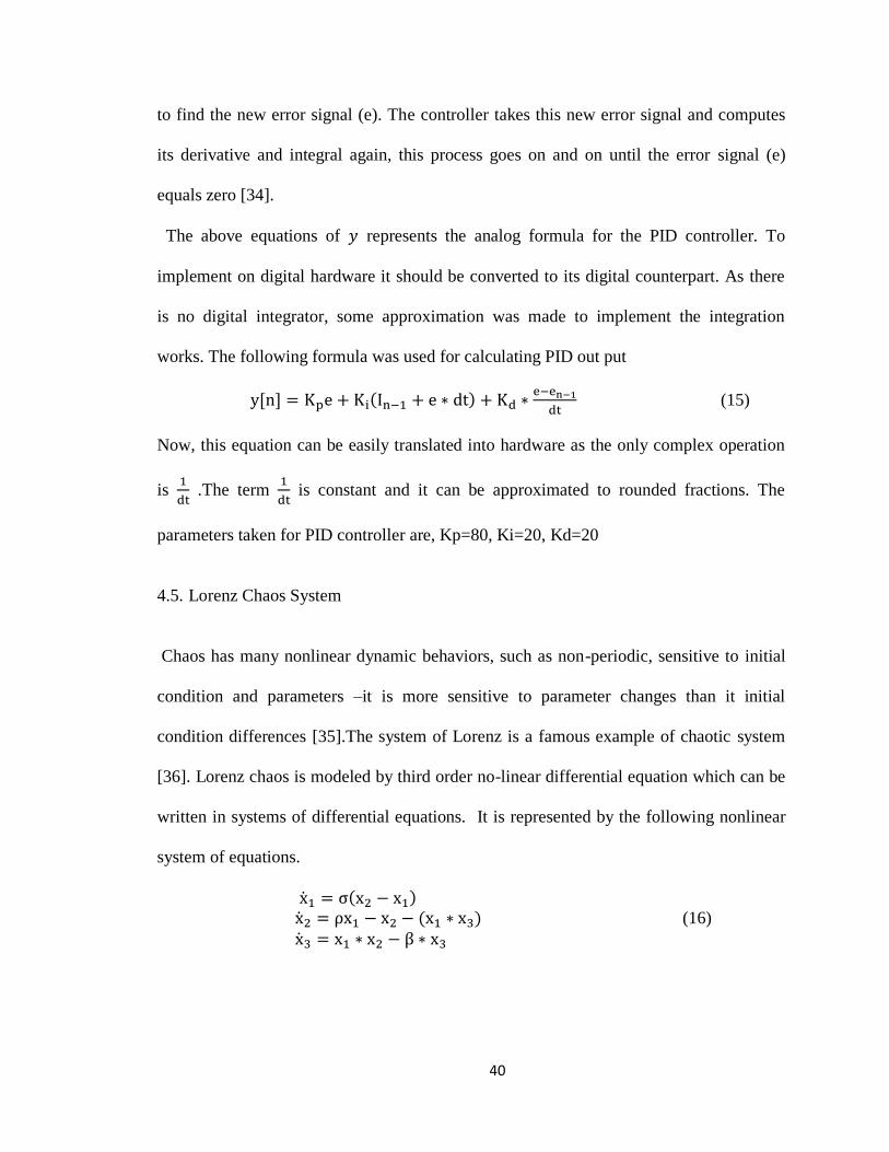
40
to find the new error signal (e). The controller takes this new error signal and computes
its derivative and integral again, this process goes on and on until the error signal (e)
equals zero [34].
The above equations of represents the analog formula for the PID controller. To
implement on digital hardware it should be converted to its digital counterpart. As there
is no digital integrator, some approximation was made to implement the integration
works. The following formula was used for calculating PID out put
(15)
Now, this equation can be easily translated into hardware as the only complex operation
is
.The term
is constant and it can be approximated to rounded fractions. The
parameters taken for PID controller are, Kp=80, Ki=20, Kd=20
4.5. Lorenz Chaos System
Chaos has many nonlinear dynamic behaviors, such as non-periodic, sensitive to initial
condition and parameters –it is more sensitive to parameter changes than it initial
condition differences [35].The system of Lorenz is a famous example of chaotic system
[36]. Lorenz chaos is modeled by third order no-linear differential equation which can be
written in systems of differential equations. It is represented by the following nonlinear
system of equations.
(16)

41
The behavior of chaotic system is high dependent on initial conditions and parameters.
It's very sensitive to initial conditions and parameters. The nature of Chaos systems is
getting attention from different researchers for different application. It is used for
encrypting data in communication system [35]. For this thesis we have taken parameters,
.
4.5.1. Control of Lorenz Chaos System
Adaptive controller of Lorenz Chaos System (LCS) designed by (Singh) has been used
and implemented in this thesis.
(17)
Where, b is unknown positive number, d(t) random disturbance input, u is the control
unit.
All algorithms of application discussed above were simulated in MATLAB/Simulink
and LabVIEW and translated into hardware and finally implemented on reconfigurable
devices. The performances of devices have been evaluated and device utilizations of
algorithms have been discussed. The following chapter explains in detail the
implementation results of these applications and platforms used for implementations.

42
CHAPTER 5
IMPLEMENTATION
This chapter deals with FPGA implementation of algorithms discussed in the previous
chapter using Xilinx System Generator (XSG) and LabVIEW FPGA Module. Software
and hardware platforms used as well as steps followed for the implementations of the
algorithms are explained in this chapter. Simulations results have been analyzed and
discussed.
5.1. Introduction to FPGA
Field Programmable Gate Arrays (FPGAs) are programmable semiconductor devices
that are based around a matrix of Configurable Logic Blocks (CLBs) connected through
programmable interconnects as shown in Figure 5.1. As opposed to Application Specific
Integrated Circuits (ASICs), where the device is custom built for the particular design,
FPGAs can be programmed to the desired application or functionality requirements [37].

43
Figure 5.1 FPGA block diagram
FPGAs allow designers to change their designs very late in the design cycle– even
after the end product has been manufactured and deployed in the field. Due to their
programmable nature, FPGAs are an ideal fit for many different markets. Xilinx is an
industry leader [37], which provides comprehensive solutions consisting of FPGA
devices, advanced software, and configurable, ready-to-use IP cores for market and
applications such as aerospace and defense, Automotive, broadcast, consumer
electronics, High performance computing, medical, wireless and wired communication,
audio, security , video and imaging. There are a lots of FPGA Vendors [38]; Xilinx,
Actel, Altera, Atmel, QuickLogic Corp, etc. Due to its popularity among other FPGA
vendors, Xilinx's current FPGA trend is seen as shown in Table 5.1 below [38].

44
Table 5.1 Xilinx FPGA comparison
Xilinx FPGA Families
Features Artix-7 Kintex-7 Virtex-7 Spartan-6 Virtex-6
Logic Cells 215,000 480,000 2,000,000 150,000 760,000
Block RAM (Mb) 13 34 68 4.8 38
DSP Slices 740 1,920 3,600 180 2016
DSP performance
(Symmetric FIR)
(GMACs)
930 2845 5335 140 2419
Transceiver Count 16 32 96 8 72
Transceiver Speed
(Gb/s) 6.6 12.5 28.05 3.2 11.18
Total transceiver BW
(Full duplex) (Gb/s) 211 800 2784 50 536
Memory interface ,
DDR3 (Mb/s) 1,066 1,866 1,866 800 1,066
PCI Express® interface X4 Gen2 X8 Gen2 X8 Gen3 X1 Gen1 x1 Gen2
Agile Mixed Signal
(AMS) /XADC Yes Yes Yes yes
Configurable AES Yes Yes Yes Yes Yes
I/O Pins 500 500 1200 576 1200
I/O Voltage (V) 1.2, .35,
1.5,1.8, 2,5,
3.3
1.2, .35,
1.5,1.8, 2,5,
3.3
1.2, .35,
1.5,1.8, 2,5,
3.3
1.2, .35,
1.5,1.8, 2,5,
3.3
1.2, .35,
1.5,1.8, 2,5,
5.2. Hardware Platforms
Different hardware platforms have been used for the implementation of algorithms in
this thesis: PC, Spartan-3A DSP, ML506-Virtex-5 FPGA Evaluation Platforms, Spartan-
3E from Xilinx and PXI 8106 embedded controller, PXI 7811R Reconfigurable I/O
(RIO) from National instruments. Implementations on Xilinx devices were done using
Xilinx System Generator and LabVIEW FPGA module was used to design the algorithms
and implement on National Instruments (NI) devices. The next section explains some
features of these devices.

45
5.2.1. Spartan-3A DSP 3400A
Spartan-3A DSP contains XtremeDSP DSP48A slices which replace the 18x18
multipliers found in the Spartan-3A devices and are based on the DSP48 blocks found in
the Virtex-4 devices. The block RAMs are also enhanced to run faster by adding an
output register. Both the block RAM and DSP48A slices in the Spartan-3A DSP devices
run at 250 MHz [39]. The following figure, Figure 5.2, shows the block diagram of
Spartan-3A DSP 3400A. This board contains Xilinx Spartan-3A DSP, XC3SD3400A-
4Fgg676 FPGA whose resource is shown in Table 5.2.
Figure 5.2 Spartan-3A DSP 3400A block diagram
5.2.2. NI PXI-8106 Embedded Controller
The National Instruments PXI-8106 is a high-performance Intel Core 2 Duo Processor
based embedded controllers for use in PXI [40]. Dual-core processors can simultaneously
execute two computing tasks, which is advantageous in multitasking environments, such

46
as Windows XP, where multiple applications run simultaneously. Two applications, such
as National Instruments LabVIEW can each execute on a separate core at the same time,
which improves overall system performance. Multithreaded applications, such as
LabVIEW, take full advantage of dual-core processors because they separate their tasks
into independent threads. A dual-core processor can simultaneously execute two of these
threads. The block diagram of this controller is shown in Figure 5.3 below.
Figure 5.3 PXI-8106 block diagram
PXI-8106 Controller contains 2.12 Intel Core 2 Duo processor, 10/100/1000BaseTX
(Gigabit) Ethernet ports, high-speed USB ports for connection to a keyboard, a mouse, a
CD-ROM/DVD-ROM drive for software installation, express card, graphic media
accelerator-for delivering sharp, smooth 3D graphic images, watchdog/trigger SMB,
GPIB (IEEE 488) controller. Window XP and Real time OS are running on the PXI 8106
controller.

47
Table 5.2 Comparison of different FPGA families Spartan 3A
DSP
(3SD3400A)
Spartan 3E
(XC3S1600E )
Spartan 3
(XC3S5000)
Virtex-5
ML506
(XC5VLX50T)
Virtex-2
(xc2v1000)
System Gates
(K)
3,400 1,600 5000 46 1000
Logic Cells 53,712 33,192 74,880
Total Slices 23,872 14,752 33,280 7,200 5120
Dedicated
Multiplier
- 36 104 48 40
DSP48 AS 126 - - 48
Max user I/O 469 36 633 480 432
Max diff I/O
Pairs
213 156 300 15
Distributed
RAM(kb)
373 231 520 480 160
Block RAM
(kb)
2268 648 1,872 2,160 720
DCM 8 8 4 6 8
Spartan-3A DSP FPGA (3SD3400A ), Virtex-5 ML506 (XC5VLX50T), Spartan 3E
(XC3S1600E) and Spartan 3 were used for implementation using Xilinx System
Generator Tool and Virtex-2, XC2V1000 FPGA was used for implementation PXI 7811R
RIO device using LabVIEW FPGA.
5.3. Software Platforms
As mentioned in Chapter 2, MATLAB R2010a/Simulink, Xilinx System Generator
13.4, ISE 13.4 and LabVIEW 8.6 were used in this thesis. Using Xilinx System
Generator (XSG) and LabVIEW FPGA models, design of system from MATLAB
/Simulink and LabVIEW, respectively, have been translated to synthesizable hardware
design. The subsequent subsection discusses the two software tools we used for the
implementation.
5.3.1. Xilinx System Generator (XSG)
Xilinx System Generator [41] is a MATLAB/Simulink blocksets, system-level
modeling tool that facilitates FPGA hardware design. It extends Simulink in many ways

48
to provide a modeling environment that is well suited to hardware design. The tool
provides high-level abstractions that are automatically compiled into an FPGA at the
push of a button. System Generator provides the ability to functional simulate hardware
design using MATLAB environment. The hardware functional simulation is verified by
comparing the hardware simulation result with the MATLAB/Simulink simulation result
because System Generator provides bit-true and cycle-true results. To say simulation is
bit-true means that at the boundaries (i.e., interfaces between System Generator blocks
and non- System Generator blocks), a value produced in simulation is bit-for-bit identical
to the corresponding value produced in hardware [41]. In a cycle-true simulation, the
values produced at Xilinx System Generator and Simulink boundaries are identical to
corresponding values produced at corresponding times in hardware. The boundaries of
the design are the points at which System Generator gateway blocks exist.
Simulink uses floating point arithmetic operations. Implementing floating point
arithmetic in hardware is, however, challenging and complex. For these reasons Xilinx
System Generator (XSG) uses fixed point format to represent all numerical values in the
system. There are blocksets in Xilinx System Generators which are used to convert the
data types floating point to fixed and fixed point back to floating points on the boundaries
(i.e interface between system generator blocks and non-system generator blocks). Xilinx
System Generator (XSG) blocks used to convert data from floating point to fixed and
fixed to floating points are called, "Gateway In and Gateway Out".
For those operations which have some complexity such as division, CORDIC and
other Xilinx IP Cores can be used and integrated into Xilinx system generators. It is also
possible to integrate other languages like VHDL, C/C++, MATLAB script, and compile

49
with other Xilinx System Generator for a particular design. System Generator token
should be included in every XSG design.
5.3.2. LabVIEW FPGA Module
The NI LabVIEW FPGA Module extends the LabVIEW graphical development
platform to target Field-Programmable Gate Arrays (FPGAs) on NI Reconfigurable I/O
(RIO) hardware. LabVIEW is well suited for FPGA programming because it clearly
represents parallelism and data flow so that users who are both experienced and
inexperienced in traditional FPGA design can effectively apply the power of
reconfigurable hardware.
Unlike tradition complex hardware language such as VHDL, which need longer
design, NI LabVIEW FPGA graphical based programming at a very high level of
abstraction facilitates the generation of FPGA codes faster than the VHDL.
5.4. Implementation Process
The implementation process involves translating each operation from the mathematical
model into hardware synthesizable codes using Xilinx System Generator and LabVIEW
FPGA module blocksets. Figure 5.4, demonstrates how a simple DSP algorithm can be
modeled using XSG from its mathematical expression. Values and parameters of each
element are assigned and configured manually until results are matched with Simulink
simulation results. The difficulty here is that there are some components of a system
which are not readily available as blocksets in Xilinx System Generator (XSG) toolbox.
For example, there is no integrator blocksets both in Xilinx System Generator and
LabVIEW FPGA Module which is required for modeling. Figure 5.5 shows how an
integrator can be constructed in Xilinx System Generator. The other important thing that

50
needs consideration is the data type parameter adjustments. To get good precision, the
data type parameters should be adjusted in such a way that it includes the range of values
that it represents. In order to get the required result, number of binary bits and binary
point should be selected appropriately to avoid errors resulted from computational
approximation because of overflow and quantization.
Figure 5.4 Simple DSP implementation using XSG
The above figure shows the implementation of simple DSP algorithm given by
mathematical model . Every System Generator diagram requires that
at least one System Generator token be placed on the diagram. This token is not
connected to anything but allow compiling the design into FPGA during hardware
implementation process. The property editor for this token allows specifying the target
netlist, device, target performance and system period. System Generator will issue an
error if this token is absent.

51
Figure 5.5 Integrator implementation in XSG
The following subsections describes the implementation of each of the control
algorithms in different approach explained in Chapter 3.
5.5. Implementation of Single Inferior Olive Neuron (ION)
From the mathematical model of ION given in Equation (1) in Chapter 4, Simulink
model is designed and translated into hardware for different implementation approach.
Software simulation has been done both in LabVIEW and MATALAB /Simulink.
5.5.1. Single ION Simulation Model
5.5.1.1. MATLAB /Simulink Model
Figure 5.6 Single ION model in Simulink

52
The MATLAB Function block contains the MATLAB Script which solves systems of
differential equations which models the ION shown in Equation (1) Chapter 4. After
running the simulation the following result is obtained.
Figure 5.7 ION Simulation result in Simulink. a) u b) v c) w d) z
Using the tic and toc MATLAB function the simulation time is determined (14.728461s).
5.5.1.2. LabVIEW Model
LabVIEW Control Design and Simulation module is used to model the ION as
shown below in Figure 5.8. The simulation is run on host machine, PC.

53
Figure 5.8 Single ION model in LabVIEW
The results obtained after running the simulation is shown below in Figure 5.9. It
can be seen that the results obtained from Simulink and LabVIEW are identical.
Figure 5.9 ION simulation result in LabVIEW.

54
5.5.1.3. LabVIEW Real-Time Model
LabVIEW Real-Time module is used to design deterministic real-time applications
which can be downloaded into dedicated NI embedded controller for reliable execution.
NI PXI-8106 embedded controller runs in two OS, Window XP and Real-Time OS. To
take the advantage of real-time system, the Real-Time target device is booted into Real-
Time OS mode and connected with the host machine through an Ethernet Cable. For the
host computer to communicate with Real-Time (RT) embedded controller, it should be
configured with in the same subnet with the RT device. Figure 5.10 shows a system
model in LabVIEW Real-Time. There are two VIs, the target VI which runs on target
device and the host VI which run on host machine. The Host VI is used for data display
of the VI running on real-time embedded controller. The communication between target
VI and host VI is via shared variables.
Figure 5.10 ION model in LabVIEW Real-Time. a) Target VI b) Host VI
Simulation result is exactly the same as the LabVIEW simulation result as shown below.

55
Figure 5.11 ION Simulation result in LabVIEW Real-Time. a) u b) v c)w d)z
5.5.2. ION HW-SW Co-Simulation
5.5.2.1. MATLAB XSG HW-SW Co-Simulation
Using the description of Hardware-Software Co-simulation in Chapter 3 Section 3.2, the
Figure 5.12 shows the hardware translated version (XSG implementation) of the ION
modeled in Simulink.

56
Figure 5.12 ION model in XSG
After running the XSG simulation, the following result is obtained.
Figure 5.13 ION HW/SW Co_simualtion result. a) u b) v c) w d) z
The elapsed time for simulation is 2.708753 seconds to generate 50,000 samples of data.

57
5.5.2.2. LabVIEW FPGA HW-SW Co-Simulation
In LabVIEW FPGA there are two main programs (VIs), one running on target device
(target VI) and the other running on host machine, (Host VI). The target VI is the
LabVIEW FPGA code for NI reconfigurable I/O (RIO) device. NI PXI-7811R RIO has
been used in this thesis. The host VI is used to display results from target VI and send
data to target VI. There are two methods to communicate with the target VI running on
the FPGA. The first method is to use Interactive Front Panel Communication to
communicate with the FPGA VI directly from the front panel window of the FPGA VI.
The second method uses programmatic FPGA Interface Communication to communicate
with the FPGA VI from a VI running on the host computer [42]. The VI running on the
host computer is called the host VI. With interactive front panel communication, the host
computer displays the FPGA VI's front panel window and the target executes the FPGA
VI block diagram as shown in the following Figure 5.14.
Figure 5.14 LabVIEW FPGA interactive front panel communication

58
With the programmatic FPGA Interface Communication, you programmatically monitor
and control an FPGA VI with a separate host VI running on the host computer as shown
in the Figure 5. 15.
Figure 5.15 Programmatic FPGA communication in LabVIEW FPGA/RT
Advantages of having host VI communicating with target device are [42]:
Process more data than that can fit on the FPGA.
Perform operations not available on the FPGA target, such as floating-point
arithmetic.
Data logging.
Run multiple VIs on the host computer.
Control the timing and sequencing of data transfer.
Control which components are visible on the front panel window because some
controls and indicators might be more important for communication than others.

59
5.5.2.3. Development Flow in LabVIEW FPGA
Creating LabVIEW FPGA VI is the first step in the FPGA application development
process. After creating the LabVIEW FPGA VI, functional behavior of the program can
be verified using simulations. Simulation in LabVIEW FPGA can be done in two ways.
One method is to compile the FPGA VI to the target and the other method is to simulate
the FPGA VI on the development computer using simulated I/O. Compiling LabVIEW
FPGA on target device takes significantly long time. Simulating the FPGA VI on
development host system enables to simulate the design faster and maximizes the
development productivity. This method enables us to debug the program using LabVIEW
debug tools such as highlighting, probes, and breakpoints before initiating compilation.
After the simulation result meets the design requirement it is then compiled to FPGA
using Xilinx ISE and bit file will be generated. Figure 5.16 shows the development
process for creating an FPGA application.
Once the LabVIEW FPGA code is compiled, LabVIEW host VI is created to integrate
the NI RIO hardware into the rest of the test and control system. The host VI uses
controls and indicators on the FPGA VI front panel to transfer data between the FPGA on
the RIO device and the host processing engine. These front panel objects are represented
as data registers within the FPGA [42].

60
Figure 5.16 LabVIEW FPGA development flow
In this thesis, the Programmatic FPGA communication has been used to transfer data
from target VI to host VI for display because of the reasons mentioned above. FIFO has
been used to transfer data from Target VI to Host VI. Using LabVIEW FPGA module a
target VI is developed which run on target device-FPGA on NI reconfigurable device.
The target VI was compiled to the target device and simulation result is displayed on host
computer. The type of FPGA used is Vertex II -1M, installed on NI PXI-7811R RIO
devices. Figures 5.17, 5.18 and Figure 5.19 show the target VI, host VI and results for
open IONs respectively.

61
Figure 5.17 ION LabVIEW FPGA target VI
Figure 5.18 ION LabVIEW FPGA host VI

62
Figure 5.19 ION HW/SW co-simulation result in LabVIEW FPGA. a) u b)v c)w d) z
5.5.3. Hardware-in-Loop (HIL) Simulation
This method involves implementing the ION in software using MATLAB /Simulink or
LabVIEW and plant (DC motor) in Xilinx System Generator. Proportional, Integral and
Derivative (PID) controller to control the DC motor has been used. The PID controller is
driven by the ION signals. The PID and DC motor Model is done, from their
mathematical model described in chapter 4 equations 15 and 13 respectively, first using
Simulink and then translated into hardware using XSG. Before going to discuss HIL, it is
important to see the behavior of the PID and DC models using software and hardware

63
simulation first. The following subsections explain the development process using
different approaches.
5.5.3.1. Implementation of PID Controller
There is a built in Simulink blocksets for PID controller for software simulation use.
For Hardware implementation of PID, however, it has be designed using equation 15 in
chapter 4. The following Figure 5.20 shows the PID controller in XSG.
Figure 5.20 PID model in XSG
5.5.3.2. Implementations of DC Motor
Figure 5.21 Shows the Simulink model of DC Motor mathematical model of which is
given in equation 13 in chapter 4.
Figure 5.21 DC motor model in Simulink
The open loop response of this model to step input signal is shown in figure 5.22 below.

64
Figure 5.22 Step response of open loop DC motor in Simulink
After PID controller is applied on DC motor as shown in Figure 5.23 below, the response
come to steady state for step input command. Figure 5.24 below shows the result step
response of PID controlled DC motor. In Simulink PID, there is interactive PID tuner to
adjust the PID parameters until fine result is obtained.
Figure 5.23 PID controlled DC motor model in Simulink

65
Figure 5.24 Step response of PID controlled closed loop DC motor in Simulink
PID controlled DC motor is also designed using LabVIEW as shown in Figure 5.25
below.
Figure 5.25 PID controlled DC motor model in LabVIEW

66
Figure 5.26 Step response of PID controlled DC motor in LabVIEW
After the LabVIEW DC Motor model is tested using the step signal, ION signal is
given as input driving signal to the Motor using the following LabVIEW VI. The output
from the DC Motor was observed and it came out to be matching with the input ION
signal driving the motor as shown in Figure 5. 27 below.
Figure 5.27 ION driven PID controlled DC motor model in LabVIEW

67
Figure 5.28 Simulation result of DC motor driven by IONs in LabVIEW. a)u b)v c)w d)z
Hardware model of PID controlled DC motor has been designed using Xilinx System
Generator (XSG) and LabVIEW FPGA as shown in Figure, 5.29 and 5.30 below. The
motor is to be controlled so that the output results match the input command. The motor
is driven by IONs as input and the output results are found to be identical to the input
signal.
Figure 5.29 Hardware model of PID controlled DC motor using XSG

68
Figure 5.30 Hardware model of PID controlled DC motor using LabVIEW FPGA
The following figure shows the hardware simulation response to step input signal.
Figure 5.31 Hardware step response of PID controlled DC motor using XSG
In HIL Simulation using MATLAB XSG, the system is set up in such a way that the
plant is implemented in hardware using Xilinx System Generator (XSG) and is driven by
ION signals which are modeled in Simulink. The plant referred to here is the PID
controlled DC Motor. To achieve HIL Simulation, fist the ION is modeled in Simulink
and simulation results are stored in MATLAB work space. The ION simulations results

69
from work space are then accessed by using Xilinx System Generator (XSG) blockset,
ROM. To access each value from the ROM, it is needed to use free up running counters
which has a size equal to the width of data defined for ROM.
Figure 5.32 HIL simulation of IONS in MATLAB-XSG block Diagram
As shown in figure 5.32 below, the out puts results of PID controlled DC motor is same
as the input driving signals, IONs for HIL simulation. This indicates, by giving the IONs
signals to the PID controlled DC motor, positions can be controlled accordingly.

70
Figure 5.33 HIL simulation result of IONs using MATLAB-XSG. a) u b)v c)w d)z
5.5.4. Hardware-in-the-Loop (HIL) Emulation
According to definition given in chapter 3 section 3.5, for hardware-in-Loop emulation
both the ION and PID controlled DC motor are implemented in Hardware and the
emulation results are tested with reference to the requirements. The Simulink and
LabVIEW software simulation results are taken as test benches. Using JTAG data is
transferred from board to MATLAB workspace and FPAG and vice versa.

71
5.5.4.1. HIL Emulation Implementation in LabVIEW FPGA
Figure 5.34 HIL emulation model in LabVIEW FPGA
As shown in figure above both ION and PID controlled DC motor are designed in
LabVIEW FPGA and compiled to the target FPGA. The PID controlled DC motor is
driven by IONs and results shown in Figure 5.35 below is obtained.

72
Figure 5.35 HIL emulation result of IONs using LabVIEW FPGA
5.5.4.2. HIL Emulation Implementation in XSG
The following figure is the XSG code, for implementation of HIL implementation in
MATLAB XSG.

73
Figure 5.36 HIL emulation model using XSG
In the above figure 5.34, the IONs are driving the PID controlled feedback controlled DC
Motor for position control. The result from the output of the DC motor is compared with
the driving ION signals and comes to be same.
Figure 5.37 I/O signal comparison for ION HIL emulation in XSG

74
5.5.5. Hardware Emulation
Hardware emulation is used to describe the implementation of each components ION,
PID, and DC motor purely in hardware. The results are tested for the requirements and
found to be matching. (To avoid repetition, I have not put each result here.)
5.6. Implementation of Synchronizations of IONs
In the following subsections the synchronization of IONs, two and three IONs using
simple gain feedback and Filter controller is studied.
5.6.1. Implementation Synchronizations of Two IONs Using Gain Controller.
5.6.1.1. Simulation
5.6.1.1.1. MATALAB/Simulink Simulation
Figure 5.38 Two IONs synchronization model in MATLAB/Simulink
In the above model the synchronization MATLAB code has been embedded in
MATLAB Function block. The following result is obtained after running the simulation.

75
Figure 5.39 Two ION synchronization result with gain controller in Simulink. a)u1,u2
b)v1,v2 c)w1,w2 d)z1,z2
5.6.1.1.2. LabVIEW Simulation
LabVIEW block diagram for the synchronization of two IONs with gain feedback
controller is illustrated in Figure5.39.

76
Figure 5.40 Two IONs synch with gain controller LabVIEW block diagram
Figure 5.41 Two IONs sync with gain controller result in LabVIEW a)u1,u2 b)v1,v2
c)w1,w2 d)z1,z2

77
5.6.1.1.3. LabVIEW Real-Time Simulation
LabVIEW Real-Time simulation is the same as LabVIEW simulation except running
on PXI-8106 controller target operating in Real-Time Operating System (RTOS).
Figure 5.42 Two IONs sync with gain controller result in LabVIEW RT a) u1,u2 b)v1,v2 c)
w1,w2 d) z1,z2
5.6.1.2. Hardware-Software Co-Simulation

78
5.6.1.2.1. Using MATLAB XSG
Figure 5.43 XSG model of two IONs sync with gain controller

79
Figure 5.44 HW-SW co-sim result of two IONs sync using gain controller in XSG. a)
u1,u2 b)v1,v2 c) w1,w2 d)z1,z2 e) Iext
5.6.1.2.2. Using LabVIEW FPGA
The LabVIEW FPGA block diagram is basically the same as that for pure LabVIEW
simulation. In LabVIEW FPGA, however, FPGA resources such as FIFO, has been added
and FPGA module is used to add the FPGA resources.

80
Figure 5.45 LabVIEW FPGA model of HW-SW co-sim of two IONs with gain
controller
Figure 5.46 HW-SW co-sim result of two IONs sync using gain controller in LabVIEW
FPGA a) u1,u2 b)v1,v2 c)w1,w2 d) z1,z2.
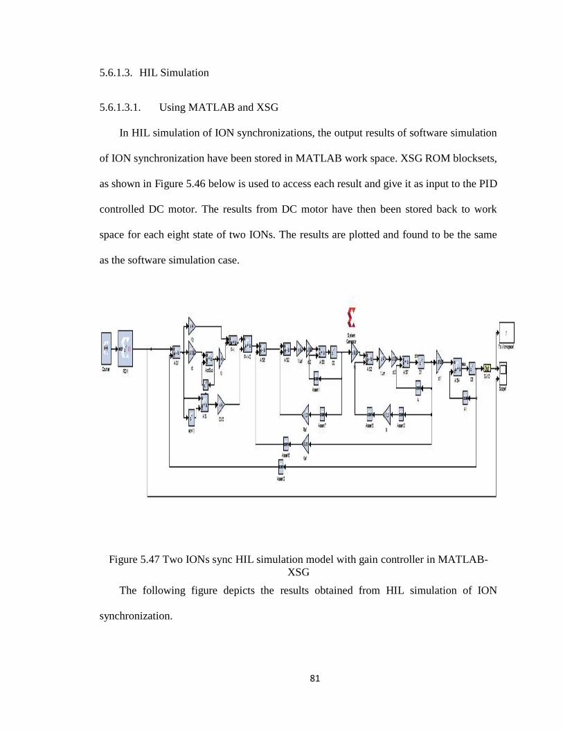
81
5.6.1.3. HIL Simulation
5.6.1.3.1. Using MATLAB and XSG
In HIL simulation of ION synchronizations, the output results of software simulation
of ION synchronization have been stored in MATLAB work space. XSG ROM blocksets,
as shown in Figure 5.46 below is used to access each result and give it as input to the PID
controlled DC motor. The results from DC motor have then been stored back to work
space for each eight state of two IONs. The results are plotted and found to be the same
as the software simulation case.
Figure 5.47 Two IONs sync HIL simulation model with gain controller in MATLAB-
XSG
The following figure depicts the results obtained from HIL simulation of ION
synchronization.

82
Figure 5.48 Two IONs sync with gain controller HIL simulation result in MATLAB-
XSG a) u1,u2 b)v1,v2 c) w1,w2 d) z1,z2
5.6.1.3.2. Using LabVIEW and LabVIEW FPGA
In LabVIEW FPGA HIL simulation, the ION is designed in LabVIEW and run on host
machine, PC. The PID controlled DC motor is designed in LabVIEW FPGA and run on
target device. The DC motor is taking input signals from out puts of IONs from the host
PC and gives the output back to the host PC for plotting. The communication between the
target device and host PC is done using the FIFOs. The results from the motor output are
basically same as the previous simulation results as shown in figure 5.50 below.

83
Figure 5.49 Two IONs sync with gain controller HIL simulation result in LabVIEW-
LabVIEW FPGA a) u1,u2 b) v1,v2 c) w1,w2 d) z1,z2
5.6.1.4. HIL Emulation
5.6.1.4.1. Using XSG
In MATLAB XSG and LabVIEW FPGA, Hardware-in-Loop (HIL) both the inferior
olive neuron (ION) and plant (PID Controlled DC motor) are implemented in XSG and
LabVIEW FPGA. This is similar to what has been done for Single ION HIL but
synchronized IONs are driving multiple Motors in this case. The IONs are serving as
driving input and output results from multiple Motors are compared with the inputs and
found to be the same.

84
5.6.2. Synchronizations of Two IONs Using Filter Feedback Controller
5.6.2.1. HW-SW Co-Simulation
5.6.2.1.1. Using XSG
XSG implementation has been done for HW-SW Co-simulation of ION Synchronization
using filter controller. From its mathematical model described in Equation 12 in Chapter
4, the hardware design of filter feedback controller used done in XSG as shown in Figure
5. 51. The results obtained basically identical to that of in gain feedback control case.
Figure 5.50 Hardware model of filter feedback controller model in XSG
It can be seen from the result shown in Figure 5.52 that the two IONs are synchronized
but there is a delay between reference and follower ION which basically caused by the
range of values of external excitation signal (Iext1 ). The value of Iext1 taken for the
following result is fixed between the range (-.05 to .05)

85
Figure 5.51 Two IONs sync with filter feedback controller in XSG (Iext b/n -0.05 to 0.05)
a) u1,u2 b) v1,v2 c) w1,w2 d) z1,z2 e) Iext1
The delay can be minimized by limiting the value of Iext1 between smaller ranges.
Figure 5.53, shows the result after fixing Iext1 between -0.005 to .005.

86
Figure 5.52 Two IONs sync with filter feedback controller in XSG (Iext1 b/n - 0.005 to 0.005) a) u1, u2 b)v1,v2 c) w1,w2 d) z1,z2 e) Iext1
5.6.2.2. HIL Emulation
5.6.2.2.1. MATLAB XSG
Feeding the Filter feedback controller IONs into the PID controlled DC motor; the
output result from the DC motor is same as the input one.

87
Figure 5.53 HIL emulation result of two ION synch with filter feedback controller in
XSG
5.6.3. Implementation of Three IONs Synchronizations Using Gain Feedback
Controller
The following sections describe implementations of synchronizations of three IONs in
different scenarios.
5.6.3.1. HW-SW Co-Simulation
Synchronizations of IONs depend on gain of the controller. By changing the gain, and
setting it to -1, the following fine results can be obtained.
Figure 5.54 HW-SW co-sim results of three sync IONs with gain feedback controller in
XSG a) u1,u2,u3 b)v1,v2,v3 c)w1,w2,w3 d) z1,z2,z3 e) Iext1

88
As can be seen from Figure 5.54, starting from different initial conditions, each
ION states come into synchrony after some time when the external excitation signal (Iext1)
diminishes to zero ultimately.
5.6.3.2. HIL Emulation
5.6.3.2.1. Using XSG
Supplying the PID controlled DC motor with three gain feedback controlled
synchronized IONs as input, simulation results from DC motor is compared with the
input results. It can be seen from Figure 5.56 that the input and output results are
identical.

89
Figure 5.55 HIL emulation result of three ION sync with gain feedback controller in XSG a) u1,u2,u3 b) v1,v2,v3 d)w1,w2,w3 d) z1,z2,z3 e) Iext1 f) Iext2
5.6.4. Implementation of Three IONs Synch Using Filter Feedback Controller
In this section implementation three IONs using filter feedback controller is
discussed using different approaches.
5.6.4.1. HW-SW Co-Simulation using XSG

90
Figure 5. 56 HW-SW co-sim result of three IONs sync with filter feedback controller in
XSG a) u1,u2,u3 b) v1,v2,v3 c)w1,w2,w3 d) z1,z2,z3 e) Iext1
5.6.5. Implementation Three IONs Sync with Phase Shift Using Gain Feedback
Controller
To introduce phase shift in the synchronization of IONs with constant phase
differences, a delay in XSG is used. The following Subsections discuss this
implementation in different approaches.
5.6.5.1. HW-SW Co-Simulation using XSG

91
Figure 5.57 Three IONs synch with phase shift and gain feedback controller model using
XSG

92
The following figure shows the results of three IONs synchronized using gain feedback
controller. The phase shift between each respective IONs state depends on the delay
value taken.
Figure 5.58 HW-SW co-sim of three phase shifted ION sync with gain feedback
controller a) u1,u2,u3 b)v1,v2,v3 c)w1,w2,w3 d) z1,z2,z3 e) Iext1
5.6.5.2. HIL Emulation
The result obtained in this case is the same as the HW-SW co-simulation result.

93
5.6.6. Implementation Three IONs Synch with Phase Shift Filter Feedback Controller
5.6.6.1. HW-SW Co-Simulation Using XSG
Figure 5.59 Three ION sync with phase shift and filter feedback controller model in XSG

94
Figure 5.60 HW-SW co-sim of three phase shifted ION sync with filter feedback
controller in XSG a) u1,u2,u3 b) v1,v2,v3 c)w1,w2,w3 d) z1,z2,z3 e) Iext1
5.7. Implementation of Lorenz Chaos System
Lorenz chaos has been implemented both in software and hardware using
MATLAB/Simulink XSG and LabVIEW/LabVIEW FPGA.
5.7.1. Simulation
5.7.1.1. LCS using MATLAB-Simulink
The following figure show Lorenz chaos system model in Simulink.

95
Figure 5.61 Lorenz chaos system model in Simulink
Figure 5.62 Lorenz chaos system model in MATLAB Simulink
After running the model, the following result is obtained. The wave of chaos system
depends on initial conditions and parameters.

96
Figure 5.63 Simulation result of Lorenz chaos system in Simulink a) x1 b)x2 c)x3 d)x1-x2-x3
5.7.1.2. LCS Using LabVIEW
Figure 5.64 Lorenz chaos system model in LabVIEW

97
Figure 5.65 Lorenz chaos system simulation result in LabVIEW a)x1, b)x2 c)x3 d)x1-x2-x3
5.7.2. HW-SW Co-Simulation
5.7.2.1. Using XSG
Figure 5.66 Lorenz chaos system model in XSG

98
Figure 5.67 Lorenz chaos system HW-SW co-sim result in XSG a)x1 b)x2 c)x3 d)x1-x2-x3
5.7.2.2. Using LabVIEW FPGA
Figure 5.68 Lorenz chaos system model (VI) using LabVIEW FPGA
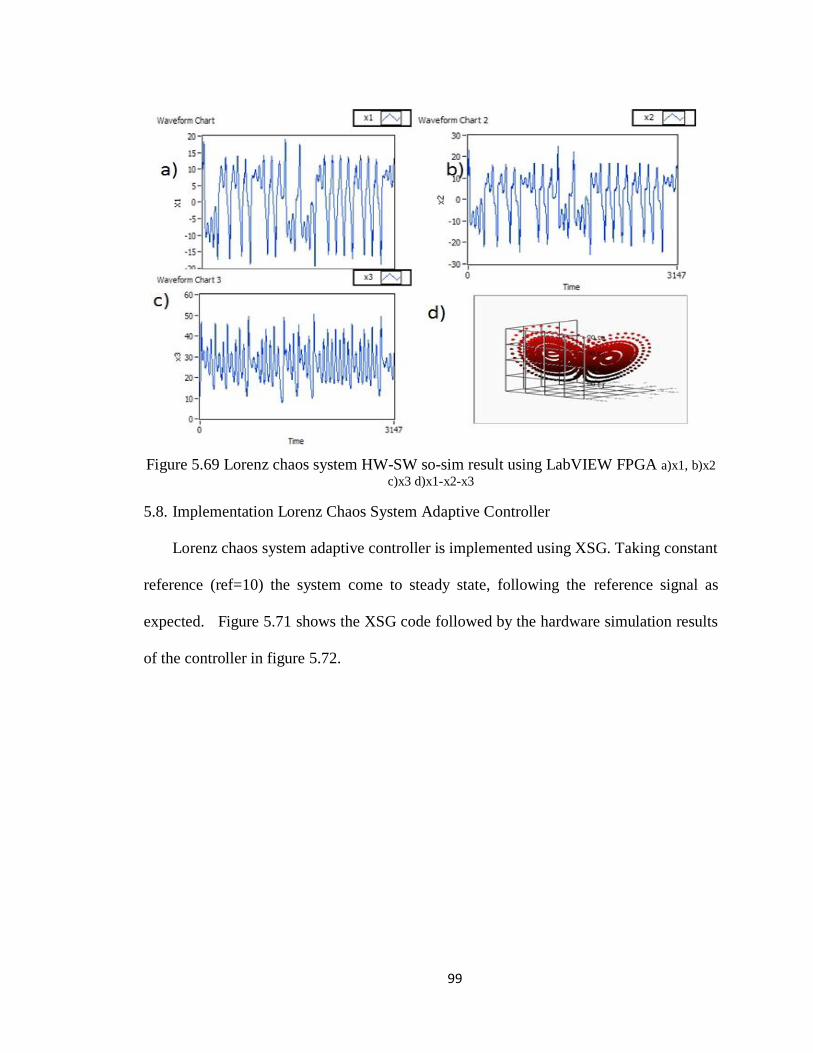
99
Figure 5.69 Lorenz chaos system HW-SW so-sim result using LabVIEW FPGA a)x1, b)x2
c)x3 d)x1-x2-x3
5.8. Implementation Lorenz Chaos System Adaptive Controller
Lorenz chaos system adaptive controller is implemented using XSG. Taking constant
reference (ref=10) the system come to steady state, following the reference signal as
expected. Figure 5.71 shows the XSG code followed by the hardware simulation results
of the controller in figure 5.72.

100
Figure 5.70 XSG model of LCS controller
Figure 5.71 LCS controller result. a) x1 b)x2 c)x3 d) u-controller command
101
CHAPTER 6
RESULTS
In this chapter, the results of algorithms implemented in this thesis has been
explained, compared and discussed. Hardware resources utilization of algorithms has
been tabulated side by side for convenience of comparison.
6.1. Hardware Resource Utilizations
Table 6.1 HW resource usage of ION and ION synchronization using filter feedback
controller on Spartan 3A DSP
From the above table, it can be concluded that the latency increases as applications
complexity increases whereas resource utilizations increases almost proportional to the
increase in program size. For example, two IONs require twice as many logic gates as
single ION does and three IONs utilize three times more logic gates than single IONs.
But the latency increases marginally in two and three IONs compared to single ION. The
results also show that there no basic differences between two and three IONs
synchronization both in device utilizations and latency.
Resources ION reference Two IONs sync Three IONs sync
with no delay
Three IONs sync
with delay
slices 734 1,485 2,236 2,236
Flip-Flops 217 416 609 609
LUTs 922 2,479 3,735 3,735
IOB 65 145 257 257
DSP Slices 10 20 30 30
BUFGMUX 1 1 1 1
L_max (ns) 39.179 41.636 43.446 43.446
f_max(MHz) 25.524 24.018 23.017 23.017

102
Table 6.2 HW resource usage of ION and ION synchronization using filter feedback
controller on Spartan Virtex-5 ML506
Looking at the results in the above table, the same conclusion made in the Table 6.1
can be drawn here. Compared to the implementation on Spartan-3A DSP, the maximum
latency is less in Virtex-5 for each respective application.
Table 6.3 HW resource usage of ION and ION sync with gain feedback controller in
XSG on Spartan 3A DSP
Resources ION Two ION sync Three ION sync
with no delay
Three ION sync
with delay
slices 734 1,467 2,331 3,275
Flip-Flops 217 990 570 2,458
LUTs 922 1885 4,013 4,955
IOB 65 145 193 193
DSP Slices 10 20 30 30
BUFGMUX 1 1 1 1
L_max 39.179 41.739 43.160 42.368
f_max 25.524 23.958 23.170 23.603
Table 6. 4 HW resource usage of ION and ION sync with gain feedback controller in
Virtex-5 ML506
Resources ION Two ION sync Three ION sync
with no delay
Three ION sync
with delay
slices 334 600 1018 1690
Flip-Flops 250 375 580 2,468
LUTs 1140 2220 3523 5374
IOB 65 129 193 193
DSP Slices 11 22 33 33
BUFGMUX 1 1 1 1
L_max 19.87 19.953 21.47 19.97
f_max 50.327 50.118 46.583 50.073
Resources ION reference Two IONs sync Three IONs sync
with no delay
Three IONs sync
with delay
slices 334 589 890 2,236
Flip-Flops 250 406 610 890
LUTs 1140 2188 3232 3232
IOB 65 145 225 225
DSP Slices 11 22 33 33
BUFGMUX 1 1 1 1
L_max (ns) 19.87 21.236 20.893 20.893
f_max(MHz) 50.327 47.09 47.863 47.863
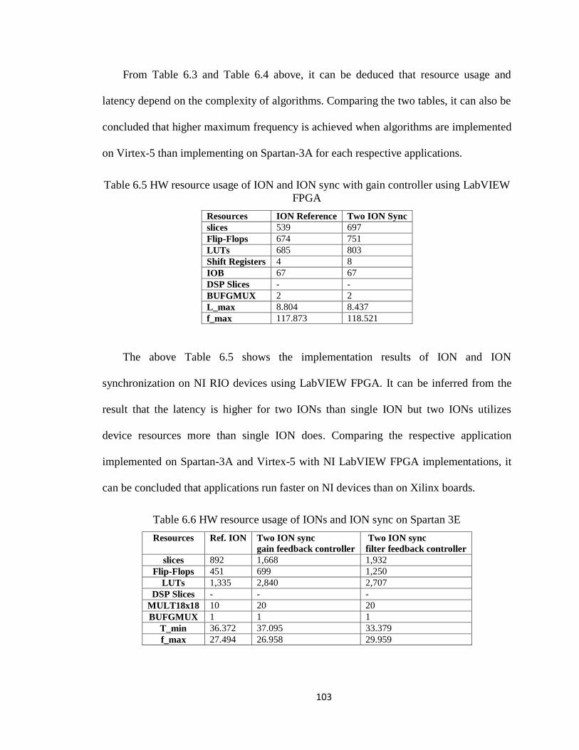
103
From Table 6.3 and Table 6.4 above, it can be deduced that resource usage and
latency depend on the complexity of algorithms. Comparing the two tables, it can also be
concluded that higher maximum frequency is achieved when algorithms are implemented
on Virtex-5 than implementing on Spartan-3A for each respective applications.
Table 6.5 HW resource usage of ION and ION sync with gain controller using LabVIEW
FPGA
Resources ION Reference Two ION Sync
slices 539 697
Flip-Flops 674 751
LUTs 685 803
Shift Registers 4 8
IOB 67 67
DSP Slices - -
BUFGMUX 2 2
L_max 8.804 8.437
f_max 117.873 118.521
The above Table 6.5 shows the implementation results of ION and ION
synchronization on NI RIO devices using LabVIEW FPGA. It can be inferred from the
result that the latency is higher for two IONs than single ION but two IONs utilizes
device resources more than single ION does. Comparing the respective application
implemented on Spartan-3A and Virtex-5 with NI LabVIEW FPGA implementations, it
can be concluded that applications run faster on NI devices than on Xilinx boards.
Table 6.6 HW resource usage of IONs and ION sync on Spartan 3E
Resources Ref. ION
Two ION sync
gain feedback controller
Two ION sync
filter feedback controller
slices 892 1,668 1,932
Flip-Flops 451 699 1,250
LUTs 1,335 2,840 2,707
DSP Slices - - -
MULT18x18 10 20 20
BUFGMUX 1 1 1
T_min 36.372 37.095 33.379
f_max 27.494 26.958 29.959

104
Table 6.7 ION HIL device utilization
Resources PID ION+PID+
DC Motor
slices 215 2,135
Flip-Flops 32 1,747
LUTs 358 3,037
IOB 65
DSP Slices 14
BUFGMUX 1 1
L_max 4.034 22.940
f_max 247.893 43.592
Table 6.8 HW resource utilization comparison of LCS
Resources LCS XSG
(xc3sd3400a )
LCS LabVIEW FPGA
slices 1,952 1,785
Flip-Flops 7,16 1,766
LUTs 3,478 2,388
IOB 193
DSP Slices 63 -
Mults18x18 - 21
RAMB16s - 8
BUFGMUX 1 2
L_max 124.747 24.747
f_max 8.016 40.4089
The above Table 6.8 shows that for the implementation of LCS, the performance of NI
devices is about 5 times faster than Xilinx device.
6.2. Comparing Different Methodologies
In this section, performance of different methodologies with respect to area,
maximum operating frequency and latency are compared and discussed.

105
Table 6.9 ION and ION synch comparison for different methodologies with respect
simulation time
Interval Real-time (sec) Step-size #Samples #osc HW CLK (ns)
ION-Sim-Simulink 400 6.72 0.014 28,635 3.5 -
ION-Sync-Simulink 400 9.467 0.013 30,804 3.5 -
ION-XSG 10 4.434 0.0001 100,000 16 -
ION-XSG-Sync 10 12.22 0.0001 100,000 16 -
ION-HW-SW 10 101.81 0.0001 100,000 16 3.00E-08
ION-HW-SW-Sync 10 118.1 0.0001 100,000 16 3.00E-08
ION-HW - 1.99E-03 3.0E-08 100,000 16 1.99E-08
ION-HW-Sync - 2.00E-03 3.0E-08 100,000 16 2.00E-08
From Table 6.9 above, it can be concluded that the processing speed of hardware is
much faster, about 1000 times faster, than that of software. It can also be seen that the
resolution, sampling period, of hardware is much smaller than that of the software.
Figure 6.1 ION and ION synch Simulation time interval comparison for different
methodologies
400 400
10 10 10 10 0 0 0
50
100
150
200
250
300
350
400
450
Interval

106
Figure 6.2 ION and ION synch real-time comparison for different methodologies
From Figure 6.1 and Figure 6.2 above, it can be inferred that the real-time
simulation for hardware is much shorter than that of the software. On the other hand, the
simulation time interval is longer for software simulation.
Figure 6.3 ION and ION synch step-size comparison for different methodologies
6.72 9.467 4.434
12.22
101.81
118.1
1.99E-03 2.00E-03 0
20
40
60
80
100
120
140
Real-time (sec)
0.014 0.013
0.0001 0.0001 0.0001 0.0001 3.0E-08 3.0E-08 0
0.002 0.004 0.006 0.008
0.01 0.012 0.014 0.016
Step-size

107
Figure 6.4 ION and ION synch No. of samples comparison for different methodologies
Figure 6.5 ION and ION sync execution time comparison for different methodologies
It can be concluded from Figure 6.5 above that the execution time in hardware is
much shorter than execution time in software. Hardware-Software Co-simulation takes
28,635 30,804
100,000 100,000 100,000 100,000 100,000 100,000
0
20,000
40,000
60,000
80,000
100,000
120,000
#Samples
4.434 12.22
42.69
11.9
42.48
89.166 94.14 75.74
115 101.81
118.1
83.3
127.81
84.52
190.789
115.97
198.67
115.2
0 0 0 0 0 0 0 0 0 0
50
100
150
200
250
Tim
e in
sec
.
XSG Simulation HW-SW Co-Simulation HW

108
longer than other methodologies as it involves configuring logic gates on the physical
devices through JTAG which results in overhead.
Figure 6.6 ION and ION sync FPGA clock period comparison for different
methodologies
Figure 6.7 FPGA area comparison of ION and ION sync for different methodologies on
Sparta-3A DSP
3.00E-08 3.00E-08 3.00E-08 3.00E-08 3.00E-08 3.00E-08 3.00E-08
2.00E-08 2.00E-08 1.99E-08 2.00E-08 2.12E-08 2.16E-08 2.12E-08 2.15E-08 2.09E-08 2.00E-08 2.09E-08
-5.00E-09
1.30E-22
5.00E-09
1.00E-08
1.50E-08
2.00E-08
2.50E-08
3.00E-08
3.50E-08
4.00E-08
CL
K p
erio
d i
n s
FPGA CLK Period
HW-SW Co-Simulation HW

109
Figure 6.8 FPGA area comparison of ION and ION sync for different methodologies on
Virtex-5 ML506
From the above two figures, Figure 6.1 and Figure 6.2, it can be concluded that the
number of FPGA logic gates utilized depends on the complexity of the algorithms.
Figure 6.9 Comparison Latency (ns) of IONs and ION synchronization
39.179
41.739 41.636 41.739 41.636
43.16 43.446
42.37
43.446
37
38
39
40
41
42
43
44
Latency L_Max (ns)

110
Figure 6.10 Comparison Max Frequency (MHz) of IONs and ION synchronization on
Virtex-5 ML506
A conclusion can be drawn from Figure 6.9 and Figure 6.10 above that the maximum
operation frequency depends on the complexity of the application implemented. The
maximum frequency for synchronizations of three IONs with delay using gain feedback
controller is greater than synchronization of three IONs with delay using filter feedback
controller. This is because the synchronization of three IONs with gain feedback
controller can be implemented by setting FPGA clock frequency to 50MHz as constraint.
But three IONs synchronization with filter feedback controller cannot be implemented at
the same 50MHz FPGA clock period. Rather, it was implemented at 30 MHz FPGA
clock period as constraint.
50.327 50.118
47.09
46.29
47.09 46.583
47.863
50.073
47.863
44
45
46
47
48
49
50
51
Frequency f_Max(MHz)
111
CHAPTER 7
CONCLUSION AND FUTUREWORK
7.1. Conclusion
In this thesis, different algorithms modeled by sets of non-linear differential equations
have been implemented on different reconfigurable hardware accelerator devices. Inferior
olive neurons (ION) and its closed-loop control synchronization implementation is the
main part of this thesis. ION synchronization controller, to control synchronization of
IONs so that they oscillate in unison, with or without phase shift has been implemented
and verified. Hardware-in-loop (HIL) of IONs with PID controlled DC motor has also
been designed and implemented. HIL has been done to test if the system works with the
real physical device. The implementation result shows that synchronization of multiple
IONs can be done using multiple motors driven by ION signal. Lorenz chaos system and
its synchronization have also been implemented.
Two software platforms were used for implementation of each algorithm and the
results have been compared. NI LabVIEW FPGA and MATLAB/ Simulink based Xilinx
System Generator (XSG) are the tools used for hardware design. Both tools are helpful in
that they are at very high level of abstraction and user friendly than traditional hardware
programming language (HDL).
Different approaches have been taken for implementations of each algorithm. First,
software simulation model were designed using MATLAB/Simulink and LabVIEW.
After the simulation results matched the requirements, the model has been translated into
hardware using XSG and LabVIEW FPGA. Hardware-Software Co-simulation, HIL

112
simulation, hardware emulation, and real-time simulation have been done and all the
results are the same for respective applications. The Simulink software simulation result
is used as test bench for the hardware simulation. Software ware simulation times are
compared with XSG and HW-SW co-simulation times.
Finally, each application has been implemented on different reconfigurable hardware
such as Xtreme DSP Spartan 3A, Spartan 3E, NI PXI 7811R and Virtex-5 ML506.
Maximum operating frequency, maximum latency and hardware resource utilizations
have been compared and discussed for different implementation.
From the implementation result, it can be concluded that the hardware resource
utilization of an algorithms depends on the complexity of the algorithm. The hardware
latency also depends on the algorithms complexity. From the result obtained, it can be
inferred that the software simulation time is much longer (1000 X) than the hardware
latency. Using different devices, an FPGA maximum operating frequency ranging from
20-50 MHz can be obtained.
7.2. Future Work
In the future work, algorithms implemented in thesis will be tested on motor using
physical hardware signals for position control. Arrays of motors will be used to test
synchronizations of IONs in the real world. Implementation of complex DSPs, CORDICs
and division operation will be addressed using Xilinx IP Cores and by incorporating
VHDL and other high level languages into XSG.

113
REFERENCES
[1] Margaret Rouse. (2007). High-Performance Computing (HPC). Search Enterprise
Linux. Retrieved August 2012, from
http://searchenterpriselinux.techtarget.com/definition / high-performance-computing
[2] Prasanna S. (2010). Xilinx white paper on High Performance Computing Using
FPGAs [white paper]. Retrieved from
http://www.xilinx.com/support/documentation/white_papers/wp375_HPC_Using_FPGAs
[3] XtremeData,Inc .(2006). XtremeData white paper on FPGA Acceleration in HPC: A
Case Study in Financial Analytics [white paper]. Retrieved from
http://www.xtremedatainc.com/pdf/FPGA_Acceleration_in_HPC.pdf ta white paper,
[4] Supercomputer. (2012). Retrieved August, 2012 from
http://en.wikipedia.org/wiki/Supercomputer
[5] National Instruments. (2012).National instruments white paper on Real-Time High-
Performance Computing with NI LabVIEW [white paper]. Retrieved from
http://www.ni.com/white-paper/11972/en
[6] Jack D. (2006, January/February).Trends in High performance computing: A
Historical Overview and Examination of Future Developments. IEEE Circuits and
Device, 23-25.
[7] Jin Woo Park, Si Hyong Park and Seung Jo Kim. (2009). Optimization with high-cost
objective function evaluations in a computing grid and an application to simulation-based
design. International Journal of High Performance Computing Applications, 23, 63-64.
doi: 10.1177/1094342008101234

114
[8] Chetan Kapoor. (2011). Creating real-time high performance computing systems
based on COTS technology. AUTOTESTCON, 2011 IEEE, 141-142.
doi: 10.1109/AUTEST.2011.6058737
[9] T. Saidani , D. Dia, W. Elhamzi, M. Atri and R. Tourki. (2009).Hardware Co-
simulation For Video Processing Using Xilinx System Generator. Proceedings of the
World Congress on Engineering, I, 2-4. ISBN: 978-988-17012-5-1
[10] Robert C. Green II, Lingfeng Wang, and Mansoor Alam. (2011). High Performance
computing for Electric Power Systems: Applications and trends. Power and Energy
Society General Meeting, 1-3. doi: 10.1109/PES.2011.6039420
[11] Netezza. (2006). Netezza white paper on Netezza Performance Server Data
Warehouse Appliance: An Architectural Comparison [white paper].Retrieved from
http://www.digident-solutions.com/resource-center/Architectural_Comparison.pdf
[12] Trends of High-Performance Computing. [2012]. Retrieved September, 2012 from
http://www.top500.org/blog/2009/05/20/top_trends_high_performance_computing
[13] Xingjun Zhang, Yanfei Ding, Yiyuan Huang, Xiaoshe Dong and Xi’an Jiaotong.
(2010). Design and Implementation of a Heterogeneous High-performance Computing
framework using Dynamic and Partial Reconfigurable FPGAs. Computer and
Information Technology (CIT), 2010 IEEE 10th International Conference on, 2329-2330.
doi: 10.1109/CIT.2010.401
[14] T. Saidani , D. Dia, W. Elhamzi, M. Atri and R. Tourki. (2009).Hardware Co-
simulation For Video Processing Using Xilinx System Generator. Proceedings of the
World Congress on Engineering, I, 2-4. ISBN: 978-988-17012-5-1
[15] National Instruments. (2010). LabVIEW user manual.

115
[16] LabVIEW.(2012). Retrieved September, 2012 from
http://en.wikipedia.org/wiki/LabVIEW
[17] LabVIEW. (2012). Retrieved September 2012 from
http://www.ni.com/LabVIEW/fpga/
[18] LabVIEW FPGA. (2008). NI white paper on optimizing your LabVIEW FPGA VIs:
Parallel Execution and pipelining [white paper]. Retrieved from
http://www.ni.com/white-paper/3749/en
[19] High-Performance Computing in Real-Time. (2008).NI White paper on High-
Performance Computing in a Real-Time Environment [white paper]. Retrieved from
http://www.ni.com/white-paper/7587/en
[20] Intel Corporation. (2010). A Real-Time HPC Approach for Optimizing Intel Multi-
Core Architectures
[21] LabVIEW Control Design and Simulation. (2011). NI white paper on what is the
LabVIEW Control Design and Simulation Module [white paper]. Retrieved from
http://www.ni.com/white-paper/11281/en
[22] Mathworks. (2012). MATLAB. Retrieved October 2012, from
http://www.mathworks.com/products/matlab/
[23] Xilix, Inc. (2008). System Generator for DSP Getting Started Guide, Release 10.1.
[24] High-Throughput DSP. (2011). National Instruments white paper on An
Introduction to High-Throughput DSP in LabVIEW FPGA [white paper].
[25] Azzaz, M.S., Tanougast, C., Sadoudi, S., Dandache, A. (2009). Real-time FPGA
Implementation of Lorenz’s Chaotic Generator for Ciphering Telecommunications.
Circuits and Systems and TAISA Conference , 2-3.

116
doi: 10.1109/NEWCAS.2009.5290495
[26]High-Throughput DSP in LabVIEW FPGA. (2011). National instruments white
paper on High-throughput DSP using in LabVIEW FPGA [white paper]. Retrieved from
http://www.ni.com/white-paper/13698/en.. [[
[27] HIL simulation. (2012). Hardware-in-the-Loop simulation. Retrieved, September
2012, from http://en.wikipedia.org/wiki/Hardware-in-the-loop_simulation.
[28] Hua, XUE, Wei-bing, LI. (2012). Implementation of Chaos Synchronization on
FPGA, AISS, V4(6), 3-4.
[29] Keum, W. Lee, Sahjendra , N. Singh. (2011). Bifurcation of orbits and synchrony in
inferior olive neurons. DOI:10.1007/s00285-011-0466-9
[30] Mathworks. (2012). Simulink. Retrieved October 2012, from
http://www.mathworks.com/products/simulink/
[31] Llinas R. (2009). Inferior olive oscillation as the temporal basis for motricity and
oscillatory reset as the basis for motor error correction. Neuroscience.
[32] Kazantsev, VB, Nekorkin, VI, Makarenko VI, Llinas, R. (2003). Olivo-cerebellar
cluster-based universal control system. PNAS, 100(22). doi:13064–13068
[33] Fasih, A., Tuan Do Trong, Chedjou, J.C., Kyamakya, K. (2009). New
Computational Modeling for Solving Higher Order ODE based on FPGA. IEEE
proceeding on Nonlinear Dynamics and Synchronization, INDS '09. 2nd International
Workshop, 50-52.
[34] Kuo, Benjamin C. (1995). Automatic Control System, 7th
ed. NJ: Prentice-Hall, Inc.

117
[35] Ali, F.H., Mahmood, H.M., Ismael, S.M.B. (2010). LabVIEW FPGA
implementation of a PID Controller for D.C. motor speed control. IEEE proceeding on
Energy, Power and Control (EPC-IQ), 2010 1st International Conference, 140-142.
[36] Xilix, Inc. (2008). System Generator for DSP Reference Guide, Release 10.1.3
[37] Desta Edosa, Keum W. Lee, Venkatesan Muthukumar, and Sahjendra N. Singh.
(2012). Hardware-Software Cosimulation of Feedback Controller for Synchronization of
Inferior Olive Neurons. MSV, WorldComp'12.
[38] FPGA. (2012). Retrieved, September 2012, from
http://www.xilinx.com/fpga/index.htm
[39] FPGA vendor. (2012). Retrieved, October 2012, from
http://www.fpgacentral.com/vendor/directory
[40] Xilinx, Inc. (2008). XtremeDSP Development Platform: Spartan-3A DSP 3400A
Edition User Guide.
[41] National Instruments. (2012) . NI PXI controller. Retrieved October 2012, from
http://www.ni.com/pdf/products/us/cat_pxiandpxie_8106.pdf
[42] HIL simulation. (2012). Retrieved, October 2012, from
http://en.wikipedia.org/wiki/Hardware-in-the-loop_simulation
[43] LabVIEW FPGA. (2012). Retrieved, October 2012, from
http://zone.ni.com/reference/en-XX/help/371599H-01/lvfpgaconcepts/pfi_comm/
[44] National Instruments. (2012). Developing Custom Measurement and Control I/O
Hardware with the LabVIEW FPGA Module and Reconfigurable I/O Hardware.
Retrieved, October 2012, from http://www.ni.com/white-paper/3261/en

118
[45] Djalma M.Falcao. (1996). High performance computing in power system
applications. International meeting on vector and parallel processing.
[46] Rugh, WJ. (1996). Linear System Theory. NJ: Prentice-Hall
[47] Xilinx, Inc. (2011). Spartan-3 Generation FPGA User Guide, UG331 (v1.8).
[48] Xilinx, Inc. (2009). Virtex-5 Family overview, DS100 (v5.0).
[49] Xilinx, Inc. (2005). Virtex-II Platform FPGAs: Complete Data Sheet.
[50] Vikas Gupta, K. Khare, R. P. Singh. (2011). Efficient FPGA implementation of 2nd
order digital controllers using matlab/Simulin. Asian Research Publishing Network
(ARPN), Vol 6(8).
[51] ALE System Integration. (2009). High Performance Computing using FPGAs.
National Instruments Technical Conference , 7-11.

119
VITA
Graduate College
University of Nevada Las Vegas
Degree :
Bachelor of Science Electrical Engineering, July 2007
Bahir Dar University, Bahir Dar, Ethiopia
Honors:
Tau Beta Pie
Alliance of Professionals of African Heritage
Thesis Title: hardware-software co-design, acceleration and prototyping of control
Algorithms on reconfigurable platforms
Thesis Examination Committee:
Committee Chair, Dr. Venkatesan Muthukumar, Ph.D.
Committee Member, Dr. Emma Regentova, Ph.D.
Committee Member, Dr. Singh Sahejendra, Ph.D.
Graduate College Representative, Dr. Ajoy Kumar Datta, Ph.D.