hardware interface description for the integrated power ... · english-language translations of...
TRANSCRIPT
Mary Jo W. Shalkhauser and Rigoberto RocheGlenn Research Center, Cleveland, Ohio
Hardware Interface Description for the Integrated Power, Avionics, and Software (iPAS) SpaceTelecommunications Radio System (STRS) Radio
NASA/TM—2017-219432
May 2017
https://ntrs.nasa.gov/search.jsp?R=20170004669 2018-07-20T12:40:41+00:00Z

NASA STI Program . . . in Profi le
Since its founding, NASA has been dedicated to the advancement of aeronautics and space science. The NASA Scientifi c and Technical Information (STI) Program plays a key part in helping NASA maintain this important role.
The NASA STI Program operates under the auspices of the Agency Chief Information Offi cer. It collects, organizes, provides for archiving, and disseminates NASA’s STI. The NASA STI Program provides access to the NASA Technical Report Server—Registered (NTRS Reg) and NASA Technical Report Server—Public (NTRS) thus providing one of the largest collections of aeronautical and space science STI in the world. Results are published in both non-NASA channels and by NASA in the NASA STI Report Series, which includes the following report types: • TECHNICAL PUBLICATION. Reports of
completed research or a major signifi cant phase of research that present the results of NASA programs and include extensive data or theoretical analysis. Includes compilations of signifi cant scientifi c and technical data and information deemed to be of continuing reference value. NASA counter-part of peer-reviewed formal professional papers, but has less stringent limitations on manuscript length and extent of graphic presentations.
• TECHNICAL MEMORANDUM. Scientifi c
and technical fi ndings that are preliminary or of specialized interest, e.g., “quick-release” reports, working papers, and bibliographies that contain minimal annotation. Does not contain extensive analysis.
• CONTRACTOR REPORT. Scientifi c and technical fi ndings by NASA-sponsored contractors and grantees.
• CONFERENCE PUBLICATION. Collected papers from scientifi c and technical conferences, symposia, seminars, or other meetings sponsored or co-sponsored by NASA.
• SPECIAL PUBLICATION. Scientifi c,
technical, or historical information from NASA programs, projects, and missions, often concerned with subjects having substantial public interest.
• TECHNICAL TRANSLATION. English-
language translations of foreign scientifi c and technical material pertinent to NASA’s mission.
For more information about the NASA STI program, see the following:
• Access the NASA STI program home page at http://www.sti.nasa.gov
• E-mail your question to [email protected] • Fax your question to the NASA STI
Information Desk at 757-864-6500
• Telephone the NASA STI Information Desk at 757-864-9658 • Write to:
NASA STI Program Mail Stop 148 NASA Langley Research Center Hampton, VA 23681-2199

Mary Jo W. Shalkhauser and Rigoberto RocheGlenn Research Center, Cleveland, Ohio
Hardware Interface Description for the Integrated Power, Avionics, and Software (iPAS) SpaceTelecommunications Radio System (STRS) Radio
NASA/TM—2017-219432
May 2017
National Aeronautics andSpace Administration
Glenn Research CenterCleveland, Ohio 44135

Available from
Trade names and trademarks are used in this report for identifi cation only. Their usage does not constitute an offi cial endorsement, either expressed or implied, by the National Aeronautics and
Space Administration.
Level of Review: This material has been technically reviewed by technical management.
NASA STI ProgramMail Stop 148NASA Langley Research CenterHampton, VA 23681-2199
National Technical Information Service5285 Port Royal RoadSpringfi eld, VA 22161
703-605-6000
This report is available in electronic form at http://www.sti.nasa.gov/ and http://ntrs.nasa.gov/
NASA/TM—2017-219432 1
Hardware Interface Description for the Integrated Power, Avionics, and Software (iPAS) Space Telecommunications Radio System
(STRS) Radio
Mary Jo W. Shalkhauser and Rigoberto Roche National Aeronautics and Space Administration
Glenn Research Center Cleveland, Ohio 44135
Summary
The Space Telecommunications Radio System (STRS) provides a common, consistent framework for software defined radios (SDRs) to abstract the application software from the radio platform hardware. The STRS standard aims to reduce the cost and risk of using complex, configurable, and reprogrammable radio systems across NASA missions. To promote the use of the STRS architecture for future NASA advanced exploration missions, NASA Glenn Research Center developed an STRS-compliant SDR on a radio platform used by the Advanced Exploration System program at the Johnson Space Center in their Integrated Power, Avionics, and Software (iPAS) laboratory.
Introduction
The Integrated Power, Avionics, and Software (iPAS) Space Telecommunications Radio System (STRS) radio was implemented on the Reconfigurable, Intelligently-Adaptive Communication System (RIACS) platform, currently being used for radio development at Johnson Space Center. The platform consists of a Xilinx® Virtex®-6 ML605 Evaluation Kit, an Analog Devices AD–FMCOMMS1–EBZ radiofrequency (RF) front-end board, and an Axiomtek™ eBOX620–110–FL embedded personal computer (PC) running the Ubuntu® 12.04 LTS operating system. Figure 1 shows the RIACS platform hardware. The result of this development is a very low cost STRS compliant platform that can be used for waveform developments for multiple applications.
The purpose of this document is to describe the interfaces of the RIACS platform.
Design Overview
This section presents an overview of the RIACS platform.
System Description
Figure 2 shows how the STRS standard was implemented on the RIACS platform. The general purpose module (GPM) is the implementation of the STRS command infrastructure on the iPAS radio. It houses the operating environment (OE) and presents a communication conduit for commands and data to and from the signal processing module (SPM). The GPM is where the general purpose processor (GPP) hardware is contained and accessed by the operating system running the STRS project files.
The SPM encompasses the field-programmable gate array (FPGA) design, which consists of the FPGA wrapper that implements all the interfaces to the FPGA and abstracts them from the waveform, and the waveform, which is the FPGA implementation of the radio signal processing functions. The test waveform created for the iPAS STRS radio does not fully implement all the signal processing functionality for a radio, but it exercises and demonstrates each interface in the FPGA wrapper. A future user of the platform for an STRS radio would re-use the FPGA wrapper and replace the test waveform with their own radio signal processing functions.
NASA/TM—2017-219432 2
Figure 1.—Reconfigurable, Intelligently-Adaptive Communication System (RIACS) platform. ADC,
analog-to-digital converter; DAC, digital-to-analog converter; FPGA, field-programmable gate array; RF, radiofrequency; Rx, receive; Tx, transmit.
Figure 2.—Space Telecommunications Radio System (STRS) implementation on the Reconfigurable, Intelligently-
Adaptive Communication System (RIACS) platform. ADC, analog-to-digital converter; DAC, digital-to-analog converter; FMC, FPGA Mezzanine Card; PC, personal computer; RF, radiofrequency; UDP, User Datagram Protocol.
NASA/TM—2017-219432 3
The radiofrequency module (RFM) provides the analog and RF signal processing for the iPAS STRS radio. On the transmit (Tx) side, the RF front-end board (AD–FMCOMMS1–EBZ) takes complex in-phase (I) and quadrature (Q) inputs (16 bits) into a high-speed digital-to-analog converter (DAC) to create an analog signal. The DAC output signal is up-converted to the desired RF frequency by a Q modulator. On the receive (Rx) side, the received RF signal is demodulated using direct-conversion to create I and Q analog signals. The analog signals are digitized using a 14-bit analog-to-digital converter (ADC).
General Purpose Module (GPM)
The GPM is the implementation of the STRS command infrastructure on the iPAS radio. It houses the OE and presents a communication conduit for commands and data to and from the SPM. The GPM is where the GPP hardware is contained and accessed by the operating system running the STRS project files.
The GPP hardware (eBOX620–110–FL) is used under the software implementation of the STRS Architecture; that is, STRS OE. This architecture can perform Tx-side streaming to the SPM, Rx-side streaming from the SPM, command generation, command transmission to the SPM, and command processing of responses from the SPM, all simultaneously. The GPP also controls the Ethernet communication protocol (setup in Transmission Control Protocol/Internet Protocol version 4 (TCP/IPv4)), scheduler and dynamic memory allocation of the hardware, and systemic pointing for STRS command and control interfaces.
This architecture also handles the use of specific waveform characteristics that are commanded in the iPAS test waveform application. These parameters include a pseudorandom bit sequence (PRBS) generator in the Tx side for parallel streaming to the SPM, an I and Q channel data source for parallel streaming to the SPM, a Rx-side streaming bit error rate tester (BERT), and a plotting tool for a graphical representation of the incoming data. Additional features include commands to display bit error rate (BER) from SPM BERT and from GPM BERT. Debugging tools included in this software architecture allow the user to query status bits and display any issues indicated by such bits. Additional queries are possible to obtain the status of the first in first out (FIFO) buffer during Tx-side streaming and observation of automatic speed adjustments of Tx-side packet streaming.
Signal Processing Module (SPM)
The SPM of the STRS radio architecture implements the signal processing functions on the iPAS RIACS platform using an FPGA. The FPGA design will consist of two parts: the FPGA wrapper and the test waveform. The FPGA wrapper implements each of these platform interfaces:
(1) Ethernet communication to the embedded processor for commanding and data streaming (2) DAC and ADC interface to the RF board (3) RF board control and configuration (4) FPGA clocking
The test waveform does not fully implement all the signal processing functionality for a radio, but it exercises and demonstrates each interface in the FPGA wrapper. A future user of the platform for an STRS radio would use the FPGA wrapper and replace the test waveform with their own radio signal processing functions.
The FPGA design is required to receive and process commands and provide command control and data to the test waveform. It must also receive and transmit streaming data from and to the embedded processor (i.e., the GPP). The test waveform demonstrates each FPGA wrapper interface. To test Tx-side streaming, it can perform bit error rate (BER) testing on Tx-side PRBS streaming data. It can also generate PRBS streaming data packets for a Rx-side streaming data source. The test waveform generates sine waves for the I and Q inputs to the RF transceiver. Captured I and Q outputs of the RF transceiver can be streamed to the embedded processor, where it can be plotted to demonstrate proper functionality of the RF board and its interfaces.
NASA/TM—2017-219432 4
Radiofrequency Module (RFM)
The RF front-end board (AD–FMCOMMS1–EBZ) provides the analog and RF signal processing for the iPAS STRS radio. On the Tx side, the AD–FMCOMMS1-EBZ board takes complex I and Q inputs (16 bits) into a high-speed DAC to create an analog signal. The DAC output signal is upconverted to the desired RF frequency by a quadrature modulator.
On the Rx side, the received RF signal is demodulated using direct-conversion to create I and Q analog signals. The analog signals are converted to digital data using a 14-bit ADC.
Concept of Operation
The flight computer graphical user interface (GUI) simulates the STRS commands that would originate from typical flight computer. The GPM is implemented on the embedded PC and includes the STRS OE and waveform application software. The STRS OE communicates with the waveform application through standard STRS application programming interfaces (APIs) to control and configure the waveform.
The SPM is implemented in the Xilinx® ML605 FPGA board. The FPGA consists of two parts: a FPGA wrapper and a test waveform. The FPGA wrapper abstracts the hardware interfaces from the waveform developer. The test waveform utilizes each of the hardware interfaces within the wrapper to demonstrate that the wrapper is correctly implemented. The GPM sends commands over an Ethernet port to the FPGA to control and configure the waveform. The GPM also streams packetized data to the FPGA and receives packetized streaming data from the FPGA over the same Ethernet port.
The RF front-end board (AD–FMCOMMS1–EBZ) contains a DAC, up-converter, down-converter, and an ADC. The FPGA configures the RF board using the Xilinx® Microblaze™ 32-bit Reduced Instruction Set Computer soft processor and sends I and Q data to the DAC. The FPGA also receives down-converted and sampled I and Q data from the RF board.
The test waveform demonstrates STRS commands for configuration and control of the test waveform, Tx-side streaming data operation, RF front-end board configuration, Rx-side streaming data, and STRS telemetry querying.
General Purpose Module (GPM) (Space Telecommunications Radio System (STRS) Software Design Description)
This section contains a description of the GPM.
Software Description
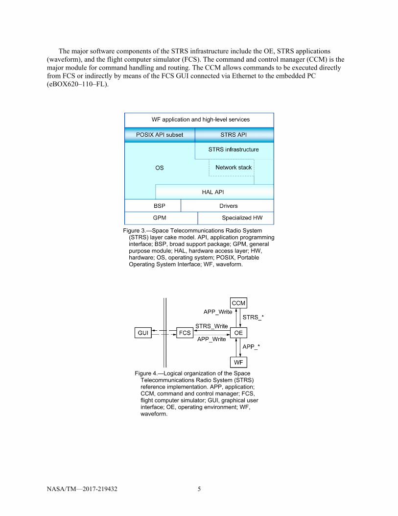
The STRS reference implementation is deployed under the STRS_Architecture_RI directory. This code is intended to demonstrate the use of the STRS architecture and to provide an STRS-capable platform for testing STRS applications. There are several software files, databases, and data files that must be installed for the software to operate. These are initialized after the successful build of the STRS_Architecture_RI project. The executable file controlling the STRS APIs is configured at make time and its pre-execution parameters are set to work with the iPAS SPM through a bash file titled “runGUI.sh.” The STRS_Architecture_RI can be represented by the STRS layer cake model to have a visual understanding of the working parts present in the code. There are several components to the architecture; these are described in more detail in the User’s Guide for the iPAS STRS Radio (Ref. 1). The STRS architecture layer cake model is illustrated in Figure 3.
Notice that the GPM, board support package (BSP), drivers, and specialized hardware are accessed by the STRS architecture through the hardware abstraction layer (HAL) APIs, so that the code can be compiled and run with the specific hardware characteristics of the memory mapping where it exists, without changes to the command and control interfacing protocol used to control the radio.
NASA/TM—2017-219432 5
The major software components of the STRS infrastructure include the OE, STRS applications (waveform), and the flight computer simulator (FCS). The command and control manager (CCM) is the major module for command handling and routing. The CCM allows commands to be executed directly from FCS or indirectly by means of the FCS GUI connected via Ethernet to the embedded PC (eBOX620–110–FL).
Figure 3.—Space Telecommunications Radio System
(STRS) layer cake model. API, application programming interface; BSP, broad support package; GPM, general purpose module; HAL, hardware access layer; HW, hardware; OS, operating system; POSIX, Portable Operating System Interface; WF, waveform.
Figure 4.—Logical organization of the Space
Telecommunications Radio System (STRS) reference implementation. APP, application; CCM, command and control manager; FCS, flight computer simulator; GUI, graphical user interface; OE, operating environment; WF, waveform.

NASA/TM—2017-219432 6
Figure 5.—Space Telecommunications Radio System (STRS) command interfaces on the general purpose
module (GPM) for the Integrated Power, Avionics, and Software (iPAS) radio. FPGA, field-programmable gate array; GUI, graphical user interface; PC, personal computer; RF, radiofrequency; RI, reference implementation; SPM, signal processing module; WFIPAS, iPAS waveform.
Command Description
The FCS accepts external commands, processes macros, and passes all other commands to the OE, which passes them on to the CCM. The CCM parses the commands and calls the appropriate method within the OE. The STRS infrastructure controls the STRS applications and other parts of the radio. When commanded, the OE calls the appropriate method in the STRS application. The STRS application implements the STRS application-provided API. The STRS applications use the STRS infrastructure-provided APIs and the Portable Operating System Interface (POSIX) to interact with the rest of the radio. Figure 4 illustrates this behavior.
Note that all commands are echoed with intermediate outputs that track the progress of execution and a final output, which indicates the completion. Invalid commands produce error messages and the STRS reference implementation continues execution. Normally one command is processed at a time. However, multiple processes are created when streaming data.
Commands are executed by invoking the waveform application iPAS waveform (WFIPAS), which takes commands from the STRS interface and sends them the SPM for control and data handling in the iPAS radio. The interfacing of these commands from the moment of generation to the point of application onto the SPM is illustrated in Figure 5.

NASA/TM—2017-219432 7
Signal Processing Module (SPM) (Field-Programmable Gate Array (FPGA) Design Description)
This section contains a description of the SPM.
Hardware Identification
This FPGA design is implemented on the Xilinx® ML605, Rev D evaluation board, which contains a Xilinx® Virtex®-6 XC6VLX240T–1FFG1156C FPGA. The AD-FMCOMMS1-EBZ RF front-end board is used for the RF front end.
Development Tools
The development tool used for this FPGA design is the Xilinx® Integrated Synthesis Environment (ISE) Design Suite System Edition version 14.4, which includes the Embedded Development Kit and Software Development Kit. The ISE Simulator (ISim) was used for design simulation of most of the VHSIC Hardware Description Language (VHDL) modules. The VHDL modules not simulated were verified in hardware.
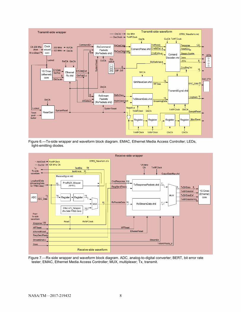
Detailed Architecture Design and Block Diagrams
Figure 6 contains a block diagram of the Tx side of the FPGA design. Most of the blocks in the diagram (and subsequent block diagrams) represent HDL code modules and are labeled with the module or instance name, so that these functions can be easily located in the code. Each block in this diagram (and also in Fig. 7) represents a VHDL module. Each of these blocks and their submodules are described in the “PLD Detailed Design” section of the Programmable Logic Device (PLD) Design Description for the iPAS STRS Radio Technical Memorandum (TM) (Ref. 2). This block diagram shows Tx-side wrapper function, which include clock generation, reset signal generation, and the modules to receive streaming and command packets and remove Ethernet headers. The block diagram also shows the Tx-side waveform functions, which include command parsing and decoding, conversion of streaming packet data into continuous streaming data, PRBS generation, and I and Q signal generation (sine waves).
Figure 7 contains the block diagram of the Rx-side of the FPGA design. The Rx-side waveform performs BER testing of PRBS or streaming data. The Rx-side wrapper packetizes command responses and Rx-side streaming data and controls their transmission over the Ethernet port.
Details of the FPGA wrapper and test waveform can be found in the PLD Design Description for the iPAS STRS Radio Technical Memorandum (TM) (Ref. 2).
NASA/TM—2017-219432 8
Figure 6.—Tx-side wrapper and waveform block diagram. EMAC, Ethernet Media Access Controller; LEDs,
light-emitting diodes.
Figure 7.—Rx-side wrapper and waveform block diagram. ADC, analog-to-digital converter; BERT, bit error rate
tester; EMAC, Ethernet Media Access Controller; MUX, multiplexer; Tx, transmit.
NASA/TM—2017-219432 9
General Purpose Module (GPM) Interfaces
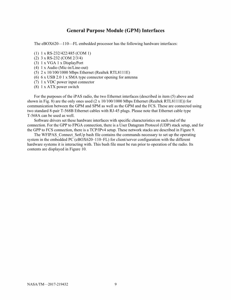
The eBOX620—110—FL embedded processor has the following hardware interfaces:
(1) 1 x RS-232/422/485 (COM 1) (2) 3 x RS-232 (COM 2/3/4) (3) 1 x VGA 1 x DisplayPort (4) 1 x Audio (Mic-in/Line-out) (5) 2 x 10/100/1000 Mbps Ethernet (Realtek RTL8111E) (6) 6 x USB 2.0 1 x SMA type connector opening for antenna (7) 1 x VDC power input connector (8) 1 x ATX power switch For the purposes of the iPAS radio, the two Ethernet interfaces (described in item (5) above and
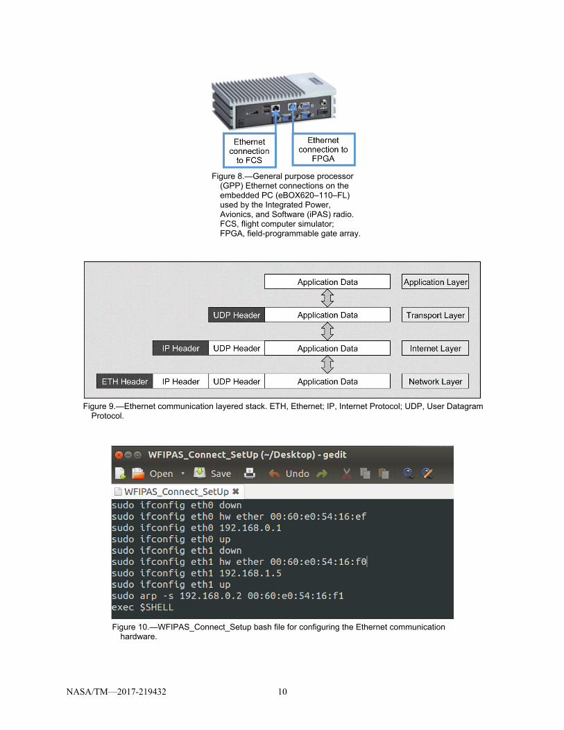
shown in Fig. 8) are the only ones used (2 x 10/100/1000 Mbps Ethernet (Realtek RTL8111E)) for communication between the GPM and SPM as well as the GPM and the FCS. These are connected using two standard 8-pair T-568B Ethernet cables with RJ-45 plugs. Please note that Ethernet cable type T-568A can be used as well.
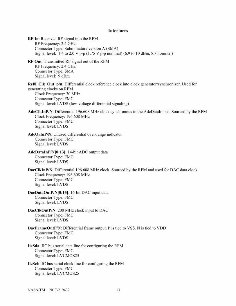
Software drivers set these hardware interfaces with specific characteristics on each end of the connection. For the GPP to FPGA connection, there is a User Datagram Protocol (UDP) stack setup, and for the GPP to FCS connection, there is a TCP/IPv4 setup. These network stacks are described in Figure 9.
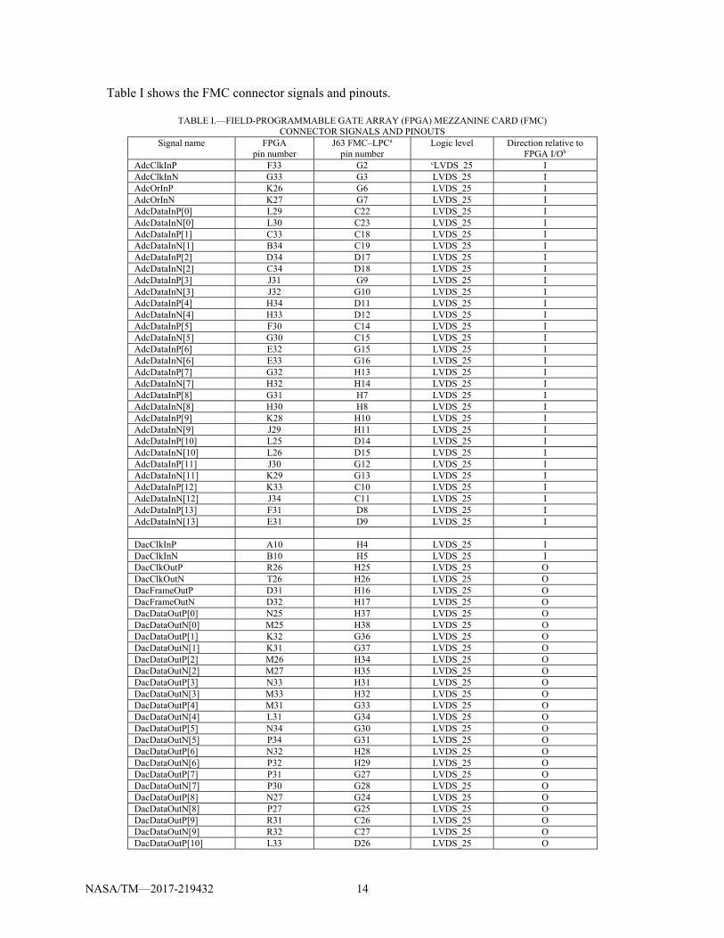
The WFIPAS_Connect_SetUp bash file contains the commands necessary to set up the operating system in the embedded PC (eBOX620–110–FL) for client/server configuration with the different hardware systems it is interacting with. This bash file must be run prior to operation of the radio. Its contents are displayed in Figure 10.
NASA/TM—2017-219432 10
Figure 8.—General purpose processor
(GPP) Ethernet connections on the embedded PC (eBOX620–110–FL) used by the Integrated Power, Avionics, and Software (iPAS) radio. FCS, flight computer simulator; FPGA, field-programmable gate array.
Figure 9.—Ethernet communication layered stack. ETH, Ethernet; IP, Internet Protocol; UDP, User Datagram
Protocol.
Figure 10.—WFIPAS_Connect_Setup bash file for configuring the Ethernet communication
hardware.

NASA/TM—2017-219432 11
If the configuration is successful, then the hardware interfaces are running, and the GPP is ready to receive and transmit data and commands. The hardware Internet Protocol (IP) configuration of the operating system is illustrated in Figure 11. Evoking the Unix command ifconfig in a terminal window allows the user to see this Ethernet configuration.
Note that a complete setup procedure for normal operation and debugging is provided in the User’s Guide for the iPAS STRS Radio (Ref. 1). This document should be read thoroughly prior to operation of the radio.
The final interface to be configured is on the Windows 7 PC. To configure this interface, the user navigates to Windows 7 Control Panel Network and Internet Network and Sharing Center. If the Ethernet cable is connected to the machine, a screen similar to Figure 12 will be observed.
Figure 11.—Ethernet configuration for the Integrated Power, Avionics, and Software (iPAS) radio.
Figure 12.—Ethernet configuration for flight computer simulator (FCS) for Integrated Power, Avionics, and Software
(iPAS) radio on Windows 7 personal computer (PC).

NASA/TM—2017-219432 12
Figure 13.—Internet Protocol (IP) configuration for flight computer simulator (FCS) for the Integrated Power, Avionics,
and Software (IPAS) radio on Windows 7 personal computer (PC). DNS, Domain Name System; Gbps, gigabits per second; I/O, input/output.
Now the local area network (LAN) connection can be configured as follows: (1) Double-click on Local Area Connection. A window will appear with connection settings. (2) Click on Properties, and then double-click on Internet Protocol Version 4. (3) Configure the IP address and select the radio button “Use the following IP address.” (4) Use 192.168.1.2 as the IP address and 192.169.1.1 as the Default Gateway. This procedure is illustrated in Figure 13. Once this procedure has been completed, all hardware interfaces for the GPM have been configured.
Radiofrequency Module (RFM) Interfaces
This section contains a description of the RFM interfaces.
Hardware Identification
The RFM consists of an RF front-end board (AD–FMCOMMS1–EBZ). The RFM was designed to provide the analog front-end for FPGA-based radio applications. Detailed information about the RF front-end board (AD–FMCOMMS1–EBZ) can be found in the Analog Devices Wiki at: https://wiki.analog.com/resources/eval/user-guides/ad-fmcomms1-ebz/hardware/functional_overview
The RF front-end board (AD–FMCOMMS1–EBZ) is a mezzanine board compatible with the Xilinx® Virtex®-6 XC6VLX240T–1FFG1156C FPGA and can plug into either FPGA Mezzanine Card (FMC) connector on the Xilinx® ML605 Rev D evaluation board. The iPAS STRS radio requires the RF front-end board (AD–FMCOMMS1–EBZ) to be inserted in only the FMC–Low Pin Count (LPC) connector. The Tx side of the high-speed analog board contains a 16-bit DAC, followed by an up-converter and a 20 dB linear amplifier. The Rx side of the board contains a down-converter, followed by a variable gain amplifier and an ADC. The board also contains clock generators/synchronizers and frequency synthesizers needed for the operation of the analog components. The board is configured by the FPGA board through an Inter-Integrated Circuit (IIC) interface. The IIC interface is converted to Serial Peripheral Interface (SPI), which is used to set up the components on the board.
NASA/TM—2017-219432 13
Interfaces
RF In: Received RF signal into the RFM RF Frequency: 2.4 GHz Connector Type: Subminiature version A (SMA) Signal level: 1.4 to 2.0 V p-p (1.75 V p-p nominal) (6.9 to 10 dBm, 8.8 nominal)
RF Out: Transmitted RF signal out of the RFM RF Frequency: 2.4 GHz Connector Type: SMA Signal level: 9 dBm
Ref0_Clk_Out_p/n: Differential clock reference clock into clock generator/synchronizer. Used for generating clocks on RFM
Clock Frequency: 30 MHz Connector Type: FMC Signal level: LVDS (low-voltage differential signaling)
AdcClkInP/N: Differential 196.608 MHz clock synchronous to the AdcDataIn bus. Sourced by the RFM Clock Frequency: 196.608 MHz Connector Type: FMC Signal level: LVDS
AdcOrInP/N: Unused differential over-range indicator Connector Type: FMC Signal level: LVDS
AdcDataInP/N[0:13]: 14-bit ADC output data Connector Type: FMC Signal level: LVDS
DacClkInP/N: Differential 196.608 MHz clock. Sourced by the RFM and used for DAC data clock Clock Frequency: 196.608 MHz Connector Type: FMC Signal level: LVDS
DacDataOutP/N[0:15]: 16-bit DAC input data Connector Type: FMC Signal level: LVDS
DacClkOutP/N: 200 MHz clock input to DAC Connector Type: FMC Signal level: LVDS
DacFrameOutP/N: Differential frame output. P is tied to VSS. N is tied to VDD Connector Type: FMC Signal level: LVDS
IicSda: IIC bus serial data line for configuring the RFM Connector Type: FMC Signal level: LVCMOS25
IicScl: IIC bus serial clock line for configuring the RFM Connector Type: FMC Signal level: LVCMOS25
NASA/TM—2017-219432 14
Table I shows the FMC connector signals and pinouts.
TABLE I.—FIELD-PROGRAMMABLE GATE ARRAY (FPGA) MEZZANINE CARD (FMC) CONNECTOR SIGNALS AND PINOUTS
Signal name FPGA pin number
J63 FMC–LPCa
pin number Logic level Direction relative to
FPGA I/Ob AdcClkInP F33 G2 cLVDS_25 I AdcClkInN G33 G3 LVDS_25 I AdcOrInP K26 G6 LVDS_25 I AdcOrInN K27 G7 LVDS_25 I AdcDataInP[0] L29 C22 LVDS_25 I AdcDataInN[0] L30 C23 LVDS_25 I AdcDataInP[1] C33 C18 LVDS_25 I AdcDataInN[1] B34 C19 LVDS_25 I AdcDataInP[2] D34 D17 LVDS_25 I AdcDataInN[2] C34 D18 LVDS_25 I AdcDataInP[3] J31 G9 LVDS_25 I AdcDataInN[3] J32 G10 LVDS_25 I AdcDataInP[4] H34 D11 LVDS_25 I AdcDataInN[4] H33 D12 LVDS_25 I AdcDataInP[5] F30 C14 LVDS_25 I AdcDataInN[5] G30 C15 LVDS_25 I AdcDataInP[6] E32 G15 LVDS_25 I AdcDataInN[6] E33 G16 LVDS_25 I AdcDataInP[7] G32 H13 LVDS_25 I AdcDataInN[7] H32 H14 LVDS_25 I AdcDataInP[8] G31 H7 LVDS_25 I AdcDataInN[8] H30 H8 LVDS_25 I AdcDataInP[9] K28 H10 LVDS_25 I AdcDataInN[9] J29 H11 LVDS_25 I AdcDataInP[10] L25 D14 LVDS_25 I AdcDataInN[10] L26 D15 LVDS_25 I AdcDataInP[11] J30 G12 LVDS_25 I AdcDataInN[11] K29 G13 LVDS_25 I AdcDataInP[12] K33 C10 LVDS_25 I AdcDataInN[12] J34 C11 LVDS_25 I AdcDataInP[13] F31 D8 LVDS_25 I AdcDataInN[13] E31 D9 LVDS_25 I DacClkInP A10 H4 LVDS_25 I DacClkInN B10 H5 LVDS_25 I DacClkOutP R26 H25 LVDS_25 O DacClkOutN T26 H26 LVDS_25 O DacFrameOutP D31 H16 LVDS_25 O DacFrameOutN D32 H17 LVDS_25 O DacDataOutP[0] N25 H37 LVDS_25 O DacDataOutN[0] M25 H38 LVDS_25 O DacDataOutP[1] K32 G36 LVDS_25 O DacDataOutN[1] K31 G37 LVDS_25 O DacDataOutP[2] M26 H34 LVDS_25 O DacDataOutN[2] M27 H35 LVDS_25 O DacDataOutP[3] N33 H31 LVDS_25 O DacDataOutN[3] M33 H32 LVDS_25 O DacDataOutP[4] M31 G33 LVDS_25 O DacDataOutN[4] L31 G34 LVDS_25 O DacDataOutP[5] N34 G30 LVDS_25 O DacDataOutN[5] P34 G31 LVDS_25 O DacDataOutP[6] N32 H28 LVDS_25 O DacDataOutN[6] P32 H29 LVDS_25 O DacDataOutP[7] P31 G27 LVDS_25 O DacDataOutN[7] P30 G28 LVDS_25 O DacDataOutP[8] N27 G24 LVDS_25 O DacDataOutN[8] P27 G25 LVDS_25 O DacDataOutP[9] R31 C26 LVDS_25 O DacDataOutN[9] R32 C27 LVDS_25 O DacDataOutP[10] L33 D26 LVDS_25 O
NASA/TM—2017-219432 15
TABLE I.—Concluded. Signal name FPGA
pin number J63 FMC–LPCa
pin number Logic level Direction relative to
FPGA I/Ob DacDataOutN[10] M32 D27 LVDS_25 O DacDataOutP[11] R28 D23 LVDS_25 O DacDataOutN[11] R27 D24 LVDS_25 O DacDataOutP[12] M30 H22 LVDS_25 O DacDataOutN[12] N30 H23 LVDS_25 O DacDataOutP[13] P29 G21 LVDS_25 O DacDataOutN[13] R29 G22 LVDS_25 O DacDataOutP[14] C32 H19 LVDS_25 O DacDataOutN[14] B32 H20 LVDS_25 O DacDataOutP[15] A33 G18 LVDS_25 O DacDataOutN[15] B33 G19 LVDS_25 O IicSda AF13 C31 LVCMOS25 IO IicScl AG13 C30 LVCMOS25 IO Ref0_Clk_Out_p N28 D20 LVDS_25 O Ref0_Clk_Out_n N29 D21 LVDS_25 O
aFPGA Mezzanine Card Low Pin Count. bInput/output. cLow-voltage differential signaling.
Signal Processing Module (SPM) Field-Programmable Gate Array (FPGA) Interfaces
This section contains a description of the SPM FPGA interfaces.
Field-Programmable Gate Array (FPGA) Wrapper
STRS requires that the FPGA wrapper for an STRS radio encompass all the possible radio FPGA interfaces. The wrapper abstracts the interfaces from the waveform, so that the waveform developer does not need to implement these interfaces. This approach also allows the platform developer to protect proprietary information about their platform from a waveform developer. The wrapper can also include any other functionality that a radio would require, like power-on-resets and clock generation, which would be common to all radios on the platform.
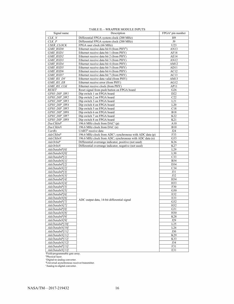
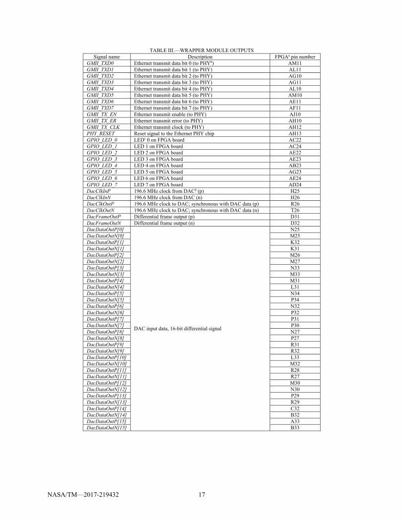
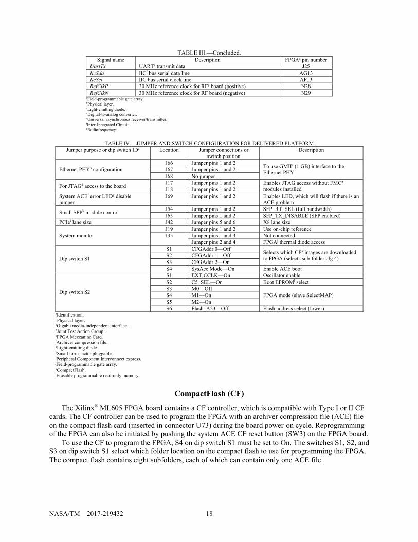
STRS_SDR_Wrapper.vhd is the top-level module in the FPGA design. This module contains the necessary basic functions of the FPGA. This wrapper module contains the FPGA Input/Output (I/O) connections to the Xilinx® ML605 board and includes submodules for generating system resets as well as system clocks. The wrapper also includes the functionality to receive command and Tx-side streaming packets (Table II) and to transmit command response and Rx-side streaming packets (Table III).
VHSIC Hardware Description Language (VHDL) Signal Polarity Convention
A signal with a “_n” at the end of the signal name like (Reset_n) is a low true (asserted low) signal. All signals without a “_n” at the end of the signal name are high true (asserted high) signals.
Xilinx® ML605 Field-Programmable Gate Array (FPGA) Board Configuration— Jumpers and Dip Switch Settings
To use the wrapper and test waveform as is, insert jumpers and set dip switches according to the listings below. Some of the jumpers are in their default locations and are not needed for the iPAS STRS radio (i.e., Peripheral Component Internet express (PCIe) lane size). If a jumper connector is not listed, no jumper is needed. Table IV shows the jumper and switch configurations for the delivered platform.
NASA/TM—2017-219432 16
TABLE II.—WRAPPER MODULE INPUTS Signal name Description FPGAa pin number
CLK_N Differential FPGA system clock (200 MHz) H9 CLK_P Differential FPGA system clock (200 MHz) J9 USER_CLOCK FPGA user clock (66 MHz) U23 GMII_RXD0 Ethernet receive data bit 0 (from PHYb) AN13 GMII_RXD1 Ethernet receive data bit 1 (from PHY) AF14 GMII_RXD2 Ethernet receive data bit 2 (from PHY) AE14 GMII_RXD3 Ethernet receive data bit 3 (from PHY) AN12 GMII_RXD4 Ethernet receive data bit 4 (from PHY) AM12 GMII_RXD5 Ethernet receive data bit 5 (from PHY) AD11 GMII_RXD6 Ethernet receive data bit 6 (from PHY) AC12 GMII_RXD7 Ethernet receive data bit 7 (from PHY) AC13 GMII_RX_DV Ethernet receive data valid (from PHY) AM13 GMII_RX_ER Ethernet receive error (from PHY) AG12 GMII_RX_CLK Ethernet receive clock (from PHY) AP11 RESET Reset signal from push button on FPGA board G26 GPIO_DIP_SW1 Dip switch 1 on FPGA board D22 GPIO_DIP_SW2 Dip switch 2 on FPGA board C22 GPIO_DIP_SW3 Dip switch 3 on FPGA board L21 GPIO_DIP_SW4 Dip switch 4 on FPGA board L20 GPIO_DIP_SW5 Dip switch 5 on FPGA board C18 GPIO_DIP_SW6 Dip switch 6 on FPGA board B18 GPIO_DIP_SW7 Dip switch 7 on FPGA board K22 GPIO_DIP_SW8 Dip switch 8 on FPGA board K21 DacClkInP 196.6 MHz clock from DACc (p) A10 DacClkInN 196.6 MHz clock from DAC (n) B10 UartRx UARTd receive data J24 AdcClkInP 196.6 MHz clock from ADCe; synchronous with ADC data (p) F33 AdcClkInN 196.6 MHz clock from ADC; synchronous with ADC data (n) G33 AdcOrInP Differential overrange indicator, positive (not used) K26 AdcOrInN Differential overrange indicator, negative (not used) K27 AdcDataInP[0]
ADC output data, 14-bit differential signal
L29 AdcDataInN[0] L30 AdcDataInP[1] C33 AdcDataInN[1] B34 AdcDataInP[2] D34 AdcDataInN[2] C34 AdcDataInP[3] J31 AdcDataInN[3] J32 AdcDataInP[4] H34 AdcDataInN[4] H33 AdcDataInP[5] F30 AdcDataInN[5] G30 AdcDataInP[6] E32 AdcDataInN[6] E33 AdcDataInP[7] G32 AdcDataInN[7] H32 AdcDataInP[8] G31 AdcDataInN[8] H30 AdcDataInP[9] K28 AdcDataInN[9] J29 AdcDataInP[10] L25 AdcDataInN[10] L26 AdcDataInP[11] J30 AdcDataInN[11] K29 AdcDataInP[12] K33 AdcDataInN[12] J34 AdcDataInP[13] F31 AdcDataInN[13] E31
aField-programmable gate array. bPhysical layer. cDigital-to-analog converter. dUniversal asynchronous receiver/transmitter. eAnalog-to-digital converter.
NASA/TM—2017-219432 17
TABLE III.—WRAPPER MODULE OUTPUTS Signal name Description FPGAa pin number
GMII_TXD0 Ethernet transmit data bit 0 (to PHYb) AM11 GMII_TXD1 Ethernet transmit data bit 1 (to PHY) AL11 GMII_TXD2 Ethernet transmit data bit 2 (to PHY) AG10 GMII_TXD3 Ethernet transmit data bit 3 (to PHY) AG11 GMII_TXD4 Ethernet transmit data bit 4 (to PHY) AL10 GMII_TXD5 Ethernet transmit data bit 5 (to PHY) AM10 GMII_TXD6 Ethernet transmit data bit 6 (to PHY) AE11 GMII_TXD7 Ethernet transmit data bit 7 (to PHY) AF11 GMII_TX_EN Ethernet transmit enable (to PHY) AJ10 GMII_TX_ER Ethernet transmit error (to PHY) AH10 GMII_TX_CLK Ethernet transmit clock (to PHY) AH12 PHY_RESET Reset signal to the Ethernet PHY chip AH13 GPIO_LED_0 LEDc 0 on FPGA board AC22 GPIO_LED_1 LED 1 on FPGA board AC24 GPIO_LED_2 LED 2 on FPGA board AE22 GPIO_LED_3 LED 3 on FPGA board AE23 GPIO_LED_4 LED 4 on FPGA board AB23 GPIO_LED_5 LED 5 on FPGA board AG23 GPIO_LED_6 LED 6 on FPGA board AE24 GPIO_LED_7 LED 7 on FPGA board AD24 DacClkInP 196.6 MHz clock from DACd (p) H25 DacClkInN 196.6 MHz clock from DAC (n) H26 DacClkOutP 196.6 MHz clock to DAC; synchronous with DAC data (p) R26 DacClkOutN 196.6 MHz clock to DAC; synchronous with DAC data (n) T26 DacFrameOutP Differential frame output (p) D31 DacFrameOutN Differential frame output (n) D32 DacDataOutP[0]
DAC input data, 16-bit differential signal
N25 DacDataOutN[0] M25 DacDataOutP[1] K32 DacDataOutN[1] K31 DacDataOutP[2] M26 DacDataOutN[2] M27 DacDataOutP[3] N33 DacDataOutN[3] M33 DacDataOutP[4] M31 DacDataOutN[4] L31 DacDataOutP[5] N34 DacDataOutN[5] P34 DacDataOutP[6] N32 DacDataOutN[6] P32 DacDataOutP[7] P31 DacDataOutN[7] P30 DacDataOutP[8] N27 DacDataOutN[8] P27 DacDataOutP[9] R31 DacDataOutN[9] R32 DacDataOutP[10] L33 DacDataOutN[10] M32 DacDataOutP[11] R28 DacDataOutN[11] R27 DacDataOutP[12] M30 DacDataOutN[12] N30 DacDataOutP[13] P29 DacDataOutN[13] R29 DacDataOutP[14] C32 DacDataOutN[14] B32 DacDataOutP[15] A33 DacDataOutN[15] B33
NASA/TM—2017-219432 18
TABLE III.—Concluded. Signal name Description FPGAa pin number
UartTx UARTe transmit data J25 IicSda IICf bus serial data line AG13 IicScl IIC bus serial clock line AF13 RefClkP 30 MHz reference clock for RFg board (positive) N28 RefClkN 30 MHz reference clock for RF board (negative) N29
aField-programmable gate array. bPhysical layer. cLight-emitting diode. dDigital-to-analog converter. eUniversal asynchronous receiver/transmitter. fInter-Integrated Circuit. gRadiofrequency.
TABLE IV.—JUMPER AND SWITCH CONFIGURATION FOR DELIVERED PLATFORM
Jumper purpose or dip switch IDa Location Jumper connections or switch position
Description
Ethernet PHYb configuration J66 Jumper pins 1 and 2
To use GMIIc (1 GB) interface to the Ethernet PHY
J67 Jumper pins 1 and 2 J68 No jumper
For JTAGd access to the board J17 Jumper pins 1 and 2 Enables JTAG access without FMCe
modules installed J18 Jumper pins 1 and 2 System ACEf error LEDg disable jumper
J69 Jumper pins 1 and 2 Enables LED, which will flash if there is an ACE problem
Small SFPh module control J54 Jumper pins 1 and 2 SFP_RT_SEL (full bandwidth) J65 Jumper pins 1 and 2 SFP_TX_DISABLE (SFP enabled)
PCIei lane size J42 Jumper pins 5 and 6 X8 lane size
System monitor J19 Jumper pins 1 and 2 Use on-chip reference J35 Jumper pins 1 and 3 Not connected
Jumper pins 2 and 4 FPGAj thermal diode access
Dip switch S1
S1 CFGAddr 0—Off Selects which CFk images are downloaded to FPGA (selects sub-folder cfg 4)
S2 CFGAddr 1—Off S3 CFGAddr 2—On S4 SysAce Mode—On Enable ACE boot
Dip switch S2
S1 EXT CCLK—On Oscillator enable S2 C5_SEL—On Boot EPROMl select S3 M0—Off
FPGA mode (slave SelectMAP) S4 M1—On S5 M2—On S6 Flash_A23—Off Flash address select (lower)
aIdentification. bPhysical layer. cGigabit media-independent interface. dJoint Test Action Group. eFPGA Mezzanine Card. fArchiver compression file. gLight-emitting diode. hSmall form-factor pluggable. iPeripheral Component Interconnect express. jField-programmable gate array. kCompactFlash. lErasable programmable read-only memory.
CompactFlash (CF)
The Xilinx® ML605 FPGA board contains a CF controller, which is compatible with Type I or II CF cards. The CF controller can be used to program the FPGA with an archiver compression file (ACE) file on the compact flash card (inserted in connector U73) during the board power-on cycle. Reprogramming of the FPGA can also be initiated by pushing the system ACE CF reset button (SW3) on the FPGA board.
To use the CF to program the FPGA, S4 on dip switch S1 must be set to On. The switches S1, S2, and S3 on dip switch S1 select which folder location on the compact flash to use for programming the FPGA. The compact flash contains eight subfolders, each of which can contain only one ACE file.
NASA/TM—2017-219432 19
Joint Test Action Group (JTAG) Interface
During waveform development, the Xilinx® Virtex®-6 FPGA on the Xilinx® ML605 FPGA board can be programmed using the Xilinx® Impact program, the ISE®-generated .bit file, a Universal Serial Bus (USB) (computer side) to mini USB cable (Xilinx® ML605 FPGA board side), and the USB JTAG connector (J22) on the board.
Field-Programmable Gate Array (FPGA) Mezzanine Card (FMC) Connector Interface to Radiofrequency (RF) Board
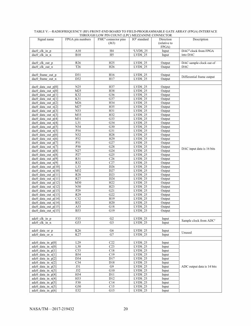
The RF front-end board (AD–FMCOMMS1–EBZ RF) interfaces with the Xilinx® Virtex®-6 FPGA through the FMC LPC connector (J63). Table V shows the signals that pass through the FMC connector between the FPGA and the RF transceiver board and the signal names, FPGA pins, FMC LPC pins, and IO standard of the signals.
Board Resources
The ML605 evaluation board has a number of onboard resources that are available to the waveform developer. Some of these resources include light-emitting diodes (LEDs), dip switches, push button switches, and clocks.
The wrapper utilizes the 200 MHz differential clock for the primary clock of the design and a push button switch for the user reset. The test waveform uses the dip switches and LEDs for a test command (read dip switches and set LEDs) and for displaying some waveform status. Therefore, the wrapper must pass the LEDs and dip switches values to and from the board resources for the test waveform. New waveform developers who do not use the dip switches or LEDs may remove them from the User Constraints File (UCF) file and from the inputs and outputs of the STRS_SDR_Wrapper module. Please refer to the ML605 Hardware User Guide (Ref. 3) for more information about the ML605 onboard resources.
Ethernet
The Xilinx® ML605 FPGA board contains an onboard Marvell Alaska® Gigabit Ethernet PHY transceiver (88E1111) for Ethernet communications. To utilize this device for packet communications with the embedded PC (eBOX620–110–FL), the Xilinx® CORE Generator™ Virtex®-6 Embedded Tri-mode Ethernet media access control (MAC) wrapper intellectual property core was generated with a 1000 Mbps transmission rate. The v6_emac_v1_5_example_design provided with the generated intellectual property core was included in the ISE® project.
Ethernet Packet Structure
Figure 14 shows the definition of the Ethernet header (MAC header, IP datagram header, and UDP header).
User Datagram Protocol (UDP) Port Numbers
Table VI shows the port numbers that were selected for each type of packet. A waveform developer may select different port source values, but must update the constants in the FPGA package (STRS_Radio_Pkg.vhd) and set up the Linux processor accordingly.
Ethernet Physical Layer (PHY)
The Ethernet PHY connection to an Ethernet cable is provided through a HALO™ HFJ11–1G01E RJ–45 connector on the Xilinx® ML605 FPGA board. The PHY connections to the FPGA device are shown in Table VII.
NASA/TM—2017-219432 20
TABLE V.—RADIOFREQUENCY (RF) FRONT-END BOARD TO FIELD-PROGRAMMABLE GATE ARRAY (FPGA) INTERFACE THROUGH LOW PIN COUNT (LPC) MEZZANINE CONNECTOR
Signal name FPGA pin numbers FMCa connector pins (J63)
IOb standard Direction (relative to
FPGA)
Description
dac0_clk_in_p A10 H4 cLVDS_25 Input DACd clock from FPGA into DAC dac0_clk_in_n B10 H5 LVDS_25 Input
dac0_clk_out_p R26 H25 LVDS_25 Output DAC sample clock out of
DAC dac0_clk_out_n T26 H26 LVDS_25 Output dac0_frame_out_p D31 H16 LVDS_25 Output
Differential frame output dac0_frame_out_n D32 H17 LVDS_25 Output dac0_data_out_p[0] N25 H37 LVDS_25 Output
DAC input data is 16 bits
dac0_data_out_n[0] M25 H38 LVDS_25 Output dac0_data_out_p[1] K32 G36 LVDS_25 Output dac0_data_out_n[1] K31 G37 LVDS_25 Output dac0_data_out_p[2] M26 H34 LVDS_25 Output dac0_data_out_n[2] M27 H35 LVDS_25 Output dac0_data_out_p[3] N33 H31 LVDS_25 Output dac0_data_out_n[3] M33 H32 LVDS_25 Output dac0_data_out_p[4] M31 G33 LVDS_25 Output dac0_data_out_n[4] L31 G34 LVDS_25 Output dac0_data_out_p[5] N34 G30 LVDS_25 Output dac0_data_out_n[5] P34 G31 LVDS_25 Output dac0_data_out_p[6] N32 H28 LVDS_25 Output dac0_data_out_n[6] P32 H29 LVDS_25 Output dac0_data_out_p[7] P31 G27 LVDS_25 Output dac0_data_out_n[7] P30 G28 LVDS_25 Output dac0_data_out_p[8] N27 G24 LVDS_25 Output dac0_data_out_n[8] P27 G25 LVDS_25 Output dac0_data_out_p[9] R31 C26 LVDS_25 Output dac0_data_out_n[9] R32 C27 LVDS_25 Output dac0_data_out_p[10] L33 D26 LVDS_25 Output dac0_data_out_n[10] M32 D27 LVDS_25 Output dac0_data_out_p[11] R28 D23 LVDS_25 Output dac0_data_out_n[11] R27 D24 LVDS_25 Output dac0_data_out_p[12] M30 H22 LVDS_25 Output dac0_data_out_n[12] N30 H23 LVDS_25 Output dac0_data_out_p[13] P29 G21 LVDS_25 Output dac0_data_out_n[13] R29 G22 LVDS_25 Output dac0_data_out_p[14] C32 H19 LVDS_25 Output dac0_data_out_n[14] B32 H20 LVDS_25 Output dac0_data_out_p[15] A33 G18 LVDS_25 Output dac0_data_out_n[15] B33 G19 LVDS_25 Output adc0_clk_in_p F33 G2 LVDS_25 Input
Sample clock from ADCe adc0_clk_in_n G33 G3 LVDS_25 Input adc0_data_or_p K26 G6 LVDS_25 Input
Unused adc0_data_or_n K27 G7 LVDS_25 Input adc0_data_in_p[0] L29 C22 LVDS_25 Input
ADC output data is 14 bits
adc0_data_in_n[0] L30 C23 LVDS_25 Input adc0_data_in_p[1] C33 C18 LVDS_25 Input adc0_data_in_n[1] B34 C19 LVDS_25 Input adc0_data_in_p[2] D34 D17 LVDS_25 Input adc0_data_in_n[2] C34 D18 LVDS_25 Input adc0_data_in_p[3] J31 G9 LVDS_25 Input adc0_data_in_n[3] J32 G10 LVDS_25 Input adc0_data_in_p[4] H34 D11 LVDS_25 Input adc0_data_in_n[4] H33 D12 LVDS_25 Input adc0_data_in_p[5] F30 C14 LVDS_25 Input adc0_data_in_n[5] G30 C15 LVDS_25 Input adc0_data_in_p[6] E32 G15 LVDS_25 Input

NASA/TM—2017-219432 21
TABLE V.—Concluded. Signal name FPGA pin numbers FMCa connector pins
(J63) IOb standard Direction
(relative to FPGA)
Description
adc0_data_in_n[6] E33 G16 LVDS_25 Input
adc0_data_in_p[7] G32 H13 LVDS_25 Input adc0_data_in_n[7] H32 H14 LVDS_25 Input adc0_data_in_p[8] G31 H7 LVDS_25 Input adc0_data_in_n[8] H30 H8 LVDS_25 Input adc0_data_in_p[9] K28 H10 LVDS_25 Input adc0_data_in_n[9] J29 H11 LVDS_25 Input adc0_data_in_p[10] L25 D14 LVDS_25 Input adc0_data_in_n[10] L26 D15 LVDS_25 Input adc0_data_in_p[11] J30 G12 LVDS_25 Input adc0_data_in_n[11] K29 G13 LVDS_25 Input adc0_data_in_p[12] K33 C10 LVDS_25 Input adc0_data_in_n[12] J34 C11 LVDS_25 Input adc0_data_in_p[13] F31 D8 LVDS_25 Input adc0_data_in_n[13] E31 D9 LVDS_25 Input ref0_clk_out_p N28 D20 LVDS_25 Output
30 MHz clock ref0_clk_out_n N29 D21 LVDS_25 Output
aFPGA Mezzanine Card. bInput/output. cLow-voltage differential signal. dDigital-to-analog converter. eAnalog-to-digital converter.
MAC header MAC destination address (6 bytes) MAC source address (6 bytes) Ethernet type
(2 bytes)
IP datagram
Version (4 bits)
IHL (4 bits)
Type of service (8 bits)
Length (IP + UDP + payload, 2 bytes)
Identification (2 bytes) Flags (3 bits) Fragment offset (13 bits)
Time to live (1 byte)
Protocol (1 byte)
IP header checksum (2 bytes)
Source IP address (4 bytes) Destination IP address (4 bytes) UDP header Source port (2 bytes) Destination port (2 bytes)
Length (UDP + payload, 2 bytes) UDP checksum (2 bytes)
Payload Various lengths
Figure 14.—Ethernet packet definition. IHL, Internet header length; IP, Internet Protocol; MAC, media access control; UDP, User Datagram Protocol.
TABLE VI.—USER DATAGRAM PROTOCOL (UDP) PORT ADDRESSES Port definition Hex value Decimal value
FPGAa port address for commands and response packets 0xD6D8 55,000 FPGA port address for streaming data packets 0xDAC0 56,000 Linux PCb port address for commands and response packets 0x8C35 35,893 Linux PC port address for streaming data packets 0x8CA0 36,000
aField-programmable gate array. bPersonal computer.

NASA/TM—2017-219432 22
TABLE VII.—ETHERNET PHYSICAL LAYER (PHY) CONNECTIONS TO FIELD-PROGRAMMABLE GATE ARRAY (FPGA) DEVICE
Signal name Description Direction FPGA pin number GMII_RXD0 Ethernet receive data bit 0 To FPGA AN13 GMII_RXD1 Ethernet receive data bit 1 To FPGA AF14 GMII_RXD2 Ethernet receive data bit 2 To FPGA AE14 GMII_RXD3 Ethernet receive data bit 3 To FPGA AN12 GMII_RXD4 Ethernet receive data bit 4 To FPGA AM12 GMII_RXD5 Ethernet receive data bit 5 To FPGA AD11 GMII_RXD6 Ethernet receive data bit 6 To FPGA AC12 GMII_RXD7 Ethernet receive data bit 7 To FPGA AC13 GMII_RX_DV Ethernet receive data valid To FPGA AM13 GMII_RX_ER Ethernet receive error To FPGA AG12 GMII_RX_CLK Ethernet receive clock To FPGA AP11 GMII_TXD0 Ethernet transmit data bit 0 To PHY AM11 GMII_TXD1 Ethernet transmit data bit 1 To PHY AL11 GMII_TXD2 Ethernet transmit data bit 2 To PHY AG10 GMII_TXD3 Ethernet transmit data bit 3 To PHY AG11 GMII_TXD4 Ethernet transmit data bit 4 To PHY AL10 GMII_TXD5 Ethernet transmit data bit 5 To PHY AM10 GMII_TXD6 Ethernet transmit data bit 6 To PHY AE11 GMII_TXD7 Ethernet transmit data bit 7 To PHY AF11 GMII_TX_EN Ethernet transmit enable To PHY AJ10 GMII_TX_ER Ethernet transmit error To PHY AH10 GMII_TX_CLK Ethernet transmit clock To PHY AH12 PHY_RESET Reset signal To PHY AH13
User Constraints File (UCF)
The FPGA UCF, STRS_Radio.ucf, defines the Xilinx® Virtex®-6 FPGA pin connections to onboard resources (LEDs, Ethernet PHY, etc.) and board connectors (FMC LPC connector, for example).
Power Supply
The Xilinx® Virtex®-6 ML605 Evaluation Kit comes with a 12 V AC-to-DC power supply. The power supply has a 6-pin plug that mates with the ML605 6-pin right-angle Mini-Fit type connector at J60. The power can be turned on and off using the SW2 slide switch mounted on the Xilinx® ML605 FPGA board. When the power supply is connected and SW2 is On, the DS25 LED will be green.
Other Available Interfaces on the ML605 Evaluation Board
The Xilinx® ML605 FPGA board contains other interfaces that are not used for the iPAS STRS radio. These interfaces, which include small form-factor pluggable (SFP), PCIe, USB to universal asynchronous receiver/transmitter (UART) Bridge, memory, Digital Video Interface (DVI), and SMA connectors, are available to a developer using the RIACS platform. More information about these interfaces can be found in the ML605 Hardware User Guide (Ref. 3).
Conclusions
The Space Telecommunications Radio System (STRS) was developed to reduce the cost and risk of using complex, configurable, and reprogrammable radio systems across multiple NASA missions. To promote the use of the STRS architecture for future NASA advanced exploration missions, NASA Glenn Research Center developed an STRS-compliant software defined radio (SDR) on a radio platform used by the Advanced Exploration System program at the NASA Johnson Space Center in their Integrated Power, Avionics, and Software (iPAS) laboratory. This platform, called the Reconfigurable, Intelligently-Adaptive Communication System (RIACS) platform, consists of easily obtainable commercial off-the-shelf hardware. This hardware interface description document defines all the platform interfaces to give NASA and other waveform developers the knowledge they need to fully understand and utilize the features of the platform.

NASA/TM—2017-219432 23
Appendix
The following abbreviations and acronyms are used within this document.
AC alternating current ACE archiver compression file ADC analog-to-digital converter API application programming interface APP application BER bit error rate BERT bit error rate tester BSP board support package CCM command and control manager CF compact flash COM communication port (serial) DAC digital-to-analog converter DC direct current dB decibels dBm decibel-milliwatts DNS Domain Name System DVI Digital Video Interface EMAC Ethernet Media Access Controller EPROM erasable programmable read-only memory ETH Ethernet FCS flight computer simulator FIFO first in first out FMC FPGA Mezzanine Card FPGA field-programmable gate array Gbps gigabits per second GMII gigabit media-independent interface GPM general purpose module GPP general purpose processor GUI graphical user interface HAL hardware abstraction layer HDL hardware description language HW hardware I in-phase ID identification IHL Internet header length IIC Inter-Integrated Circuit IO, I/O input/output IP Intellectual Property or Internet Protocol IPv4 Internet Protocol version 4 iPAS Integrated Power, Avionics, and Software ISE Integrated Synthesis Environment iSIM ISE Simulator JTAG Joint Test Action Group LAN local area network LPC Low Pin Count LED light-emitting diode LVCMOS Low Voltage Complementary Metal Oxide Semiconductor

NASA/TM—2017-219432 24
LVDS low-voltage differential signaling MAC media access control MUX multiplexer OE operating environment PC personal computer PCIe Peripheral Component Interconnect express PHY physical layer PLD programmable logic device POSIX Portable Operating System Interface PRBS pseudorandom bit sequence Q quadrature RIACS Reconfigurable, Intelligently-Adaptive Communication System RF radiofrequency RFM radiofrequency module Rx receive SDR software defined radio SFP small form-factor pluggable SMA SubMiniature version A SPI Serial Peripheral Interface SPM signal processing module STRS Space Telecommunications Radio System SW switch TCP Transmission Control Protocol TM Technical Memorandum Tx transmit UART universal asynchronous receiver/transmitter UCF User Constraints File UDP User Datagram Protocol USB Universal Serial Bus V volts VGA Video Graphics Array VHDL VHSIC Hardware Description Language WF waveform WFIPAS iPAS waveform
NASA/TM—2017-219432 25
References
1. Roche, Rigoberto: User’s Guide for the iPAS STRS Radio. NASA, to be published, 2017. 2. Shalkhauser, Mary Jo W.: Programmable Logic Device (PLD) Design Description for the Integrated
Power Avionics and Software (iPAS) Space Telecommunications Radio System (STRS) Radio. NASA/TM—2017-219429, to be published, 2017.
3. Xilinx: ML605 Hardware User Guide. 2012. http://www.xilinx.com/support/documentation/boards_and_kits/ug534.pdf Accessed Feb. 10, 2017.