hardware acceleration for eda algorithms - uclacadlab.cs.ucla.edu/~cong/slides/papa11.pdf · case...
TRANSCRIPT

1
1
Hardware acceleration for EDA algorithms
Jason Cong
Director, Center for Domain-Specific Computing UCLA Computer Science Department
[email protected] www.cdsc.ucla.edu
2
Outline Parallelization
Customization
Automation

2
3
Rise of Multi-core Processors
Nvidia's GT200 GPU (30*8 = 240 cores)
Sony-Toshiba-IBM Cell Processor(1PPE+8SPE)
Sun Rock processor (4*4 = 16 cores)
AMD 6900 series GPU 384 VLIW4 cores
4
Outline Parallelization
Customization
Automation
3
5
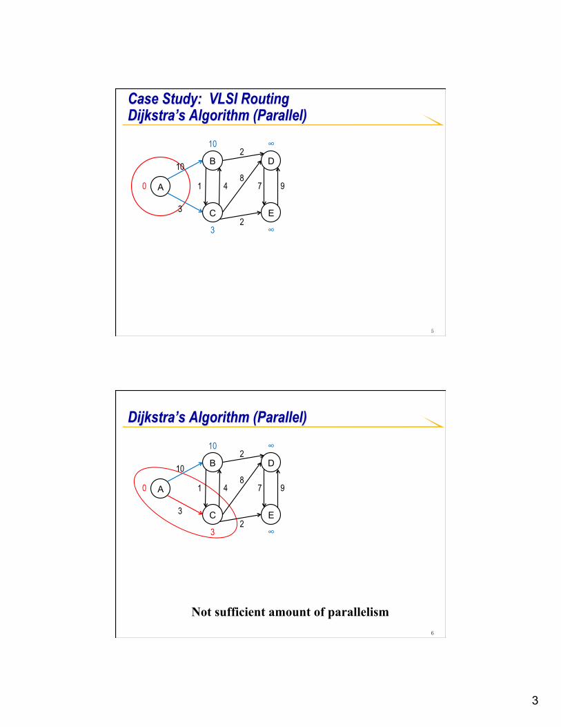
Case Study: VLSI Routing Dijkstra’s Algorithm (Parallel)
A
C
B
E
D 10
3
2
8
2
1 4 7 9
10
3
∞
∞
0
6
Dijkstra’s Algorithm (Parallel)
A
C
B
E
D 10
3
2
8
2
1 4 7 9
10
3
∞
∞
0
Not sufficient amount of parallelism

4
7
Negotiated Congestion Routing
UCLA VLSICAD LAB 7
S1 S2
A B
D1 D2
(1)
(1)
(1)
(1)
(3)
(3)
Initial iteration, routed with base cost
Cost = Present * ( Base + History ) Base: constant History: update every iteration Present: update frequently
8
Negotiated Congestion Routing
UCLA VLSICAD LAB 8
S1 S2
A B
D1 D2
(1)
(1)
(1)
(1)
(3)
(3)
Cost = Present * ( Base + History ) Base: constant History: update every iteration Present: update frequently

5
9
Negotiated Congestion Routing
UCLA VLSICAD LAB 9
S1 S2
A B
D1 D2
(1)
(1)
(1)
(1)
(3)
(3)
Cost = Present * ( Base + History ) Base: constant History: update every iteration Present: update frequently
10
Negotiated Congestion Routing
UCLA VLSICAD LAB 10
S1 S2
A B
D1 D2
(2)
(2)
(2)
(2)
(3)
(3)
2nd iteration, penalized by history
Cost = Present * ( Base + History ) Base: constant History: update every iteration Present: update frequently

6
11
Negotiated Congestion Routing
UCLA VLSICAD LAB 11
S1 S2
A B
D1 D2
(2)
(2)
(2)
(2)
(3)
(3)
Cost = Present * ( Base + History ) Base: constant History: update every iteration Present: update frequently
12
Negotiated Congestion Routing
UCLA VLSICAD LAB 12
S1 S2
A B
D1 D2
(2)
(2)
(4)
(4)
(3)
(3)
Penalized by present congestion
Cost = Present * ( Base + History ) Base: constant History: update every iteration Present: update frequently

7
13
Negotiated Congestion Routing
UCLA VLSICAD LAB 13
S1 S2
A B
D1 D2
(2)
(2)
(4)
(4)
(3)
(3)
Cost = Present * ( Base + History ) Base: constant History: update every iteration Present: update frequently
14
Coarse-Grain Parallelism [Gort & Anderson, FPL’ 10]
UCLA VLSICAD LAB 14
Proc
ess A
Process B
Process C
Cost = Present * ( Base + History ) Some nets are routed across processes Use MPI to pass “Present” information
Non-blocking issues Blocking receives The order of issues and receives is
determined by the predicted runtime For load balancing For deterministic results The best predict: number of routing
resources explored
n=1 n=2 n=3
Process B 3 2 2 …
Process A 6 2 1 …

8
15
Case Study: GPU-accelerated Analytical Global Placement [ICCAD’09] Based on code-base of mPL
§ mPL is an award-wining academic placer developed by UCLA
Mathematic formulation of Analytical Global Placement § Non-linear programming
• Minimize HPWL • Subject to density constraint • Need smoothing
Smoothing of HPWL Smoothing of density
16
Profiling Four functions that need to be accelerated
§ Native force § Bin density § Density smoothing § Spreading force
Other functions include § Parsing / IO § Clustering § Less than 10% for IBM01 § Less than 4% for larger examples
Profiling graph for IBM01
NativeForce
BinDensity
DensitySmoothing
SpreadingForce
Others

9
17
Native Force Computation Circuit netlist is essentially hypergraphs
§ Nodes (Modules), hyperedges, pins
Native force computation § Nested loop:
§ Parallelize outer loop or inner loop? § Improve the load-balancing through sorting of the loop bounds
Loop over different modules Loop over different pins
Loop over different hyperedges Loop over different pins
and/or
18
Native Force Computation
∑ ∑∑
∑ ∑∑
∈ ∈
−−
∈
∈ ∈
−−
∈
−−=
−−=
)( ))((
//
))((
//
)( ))((
//
))((
//
))/()/((
))/()/((
mpinsp phyperedgepinsq
yy
phyperedgepinsq
yyym
mpinsp phyperedgepinsq
xx
phyperedgepinsq
xxxm
qpqp
qpqp
eeeenativeF
eeeenativeF
ηηηη
ηηηη
How does the sequential version compute?
Step 1 Step 2 Step 3
M1
M3 M2
H1 H2
H3
P1 P2
P3
P4
P5
P6
Step 1 for H1,H2,H3
Step 2 for P1~P6
Step 3 for M1,M2,M3
Step 1 for H1 Step 2 for P1,P3
Step 3 update for M1,M2 Step 1 for H2
Step 2 for P2,P5 Step 3 update for M1,M3
Step 1 for H3 Step 2 for P4,P6
Step 3 update for M2,M3 Method1
Method2
The original sequential code uses method 1
Time

10
19
Parallelizing Native Force Computation (Method 1)
Parallelize outer loop (for different hyperedges)
Parallelize inner loop (inside each step) § Tree-adder-like reduction
Issues: § Paralleling outer loop needs to use
atomic operations (slow) § Tree-adder-like reduction is not very efficient for small reductions
Step 1 for H1 Step 2 for P1,P3
Step 3 update for M1,M2
Step 1 for H2 Step 2 for P2,P5
Step 3 update for M1,M3
Step 1 for H3 Step 2 for P4,P6
Step 3 update for M2,M3
Time
+ + + + + + + + + + + +
+ + +
20
Parallelizing Native Force Computation (Method 2) Parallelize outer loop (for different hyperedges / modules)
§ No atomic operation needed § Explicit global synchronization after step 1 finishes
Parallelize inner loop (inside each step) § Tree-adder-like reduction
Further optimization § Load balancing when paralleling outer loop
• Sorting of the loop bounds (reduce the impact the divergence within the wrap)
§ Combination of two schemes • Use tree-adder-like reduction only for large reduction
Step 1 for H1
Step 2 for P1,P2 Step 3 for M1
Step 1 for H2
Step 2 for P3,P4 Step 3 for M2
Step 1 for H3
Step 2 for P5,P6 Step 3 for M3
Time

11
21
Other Functions Bin-density computation
§ Count the total module area that overlaps with the bins • Process module by module • For each module, update the bin-density for the bins it overlaps with
§ Either parallelize computation between different modules § Or parallelize computation for different bins due to one specific module
Density smoothing § Using 2D DCT/IDCT
Spreading force computation § Use texture lookup to save the effort in interpolation § Parallelize computation for different modules
22
Experiment Setup Tesla C1060
§ 30*8 cores § 4GB device memory
Test suites § ICCAD’04 mix-size benchmarks § PEKO suites § PEKU suites § ISPD’06 placement contest benchmarks
Software reference runs on single core of Xeon E5405(2.0G)

12
23
Experiment Results: Speedup
IBM01
IBM05
IBM10
IBM15
PEKO01
PEKO05
PEKO10
PEKO15
PEKO18
PEKU01
PEKU05
PEKU10
PEKU15
adaptec5
newblue1
newblue3
newblue4
newblue6
IBM18
PEKU18
newblue7
newblue5
newblue2
0
5
10
15
20
25
30
24
Experiment Results: WL Degradation (cont)
adaptec5
newblue1
newblue2
newblue3
newblue4
newblue5
newblue6newblue7
-2
-1
0
1
2
3
4
GP_WL degradation(%)
DP_WL degradation (%)

13
25
Summary of the Results We implemented the critical parts of mPL global placer
onto GPU § Obtained avg ~15X speedup § Avg ~1% GP WL degradation § Avg ~0.3% DP WL degradation § Some examples see relatively large perturbations on WL
• The algorithm itself may be sensitive to numerical errors
Detailed placement not yet accelerated § We are working on this
26
Lessons Learned Degree of parallelization
Architecture specific issues for efficient implementation § Atomic operation
§ Reduction
§ Coalescing
§ …

14
27
Outline Parallelization
Customization
Automation
28
The Power Barrier and Current Solution
Parallelization
• 10’s to 100’s cores in a processor
• 1000’s to 10,000’s servers in a data center
Source : Shekhar Borkar, Intel

15
29
Cost and Energy are Still a Big Issue …
Cost of computing • HW acquisition
• Energy bill
• Heat removal
• Space
• …
30
Next Significant Opportunity -- Customization
Parallelization
Customization
Adapt the architecture to Application domain

16
31
[1] Amphion CS5230 on Virtex2 + Xilinx Virtex2 Power Estimator
[2] Dag Arne Osvik: 544 cycles AES – ECB on StrongArm SA-1110
[3] Helger Lipmaa PIII assembly handcoded + Intel Pentium III (1.13 GHz) Datasheet
[4] gcc, 1 mW/MHz @ 120 Mhz Sparc – assumes 0.25 u CMOS
[5] Java on KVM (Sun J2ME, non-JIT) on 1 mW/MHz @ 120 MHz Sparc – assumes 0.25 u CMOS
Potential of Customization
648 Mbits/sec Asm
Pentium III [3] 41.4 W 0.015 (1/800)
Java [5] Emb. Sparc 450 bits/sec 120 mW
0.0000037 (1/3,000,000)
C Emb. Sparc [4] 133 Kbits/sec 0.0011 (1/10,000)
350 mW
Power
1.32 Gbit/sec FPGA [1]
11 (1/1) Ø 3.84 Gbits/sec 0.18µm CMOS
Figure of Merit (Gb/s/W)
Throughput AES 128bit key 128bit data
490 mW 2.7 (1/4)
120 mW
ASM StrongARM [2] 240 mW 0.13 (1/85) 31 Mbit/sec
Source: P. Schaumont, and I. Verbauwhede, "Domain specific codesign for embedded security," IEEE Computer 36(4), 2003.
32 4
Emulation at NVIDIA
Mike Butts - RAMP - August, 2010
One of the largest emulation labs in the world
• In 1995, CEO Jensen Huang “spent $1 million, a third of the company’s cash, on a technology known as emulation, which allows engineers to play with virtual copies of their graphics chips before they put them into silicon. That allowed Nvidia to speed a new graphics chip to market every six to nine months, a pace the company has sustained ever since.” - from Forbes, 1/7/08

17
33
Another Successful Example - Brion Technologies § Computational lithography with FPGA acceleration § Each server node is equipped by 2 CPUs and 4 FPGAs [Cao’04]
• Looking at performance/accuracy trade-offs of FFTs
Source: System and method for lithography simulation, US patent 7117477 (by Brion Technologies)
34
Acquisition by ASML

18
35
Acceleration of Lithographic Simulation [FPGA’08]
15X+ Performance Improvement vs. AMD Opteron 2.2GHz Processor
Close to 100X improvement on energy efficiency § 15W in FPGA comparing with 86W in Opteron
Lithography simulation § Simulate the optical imaging process
§ Computational intensive; very slow for full-chip simulation
XtremeData X1000 development system (AMD Opteron + Altera StratixII EP2S180)
AutoPilotTM Synthesis Tool
Algorithm in C
Ι(x,y) = Σ λκ * | Σ τ [ψκ(x-x1, y-y1) -
ψκ(x-x2, y-y1) + ψκ(x-x2, y-y2) - ψκ(x-x1, y-y2)] |2
36
Imaging Equations (n) (n) (n) (n)
k 1 1 k 2 1 2k (n) (n) (n) (n)
1 n=1 k 2 2 k 1 2
[ (x-x , y-y ) - (x-x , y-y )I(x,y) = | |
+ (x-x , y-y ) - (x-x , y-y )]
K N
k
τ ϕ ϕλ
ϕ ϕ=∑ ∑
I(x,y) image intensity at (x,y) ψk(x,y) kth kernel φk(x,y) kth eigenvector (x1,y1)(x2, y2) (x1,y2) (x2,y1) layout corners τ mask transmittance
Pseudo code of the Imaging Equation
Loop over different rectangles
Loop over kernels
Loop over pixels
k k(x,y) = Q(x,y) (x,y)ϕ φ⊗

19
37
Keys in the Implementation Loop interchange
Memory partitioning § The look-up table should provide a very high bandwidth to the
computing logics § Not trivial because access involves indirect access § We devised a scheme that partitions the (on-chip) memory
• Parallel access, and conflict-free • Further automations on memory partitioning
Loop interchange Loop over pixels
Loop over kernels
Loop over layout corners
Loop over kernels
Loop over layout corners
Loop over pixels We
parallelized this loop
38
Keys in the Implementation Memory partitioning
partition 1 partition 2 partition 3 partition 4
Kernel Array Image Partial Sum Array
partition 1 partition 2 partition 3 partition 4

20
39
Keys in the Implementation Other optimizations
§ Use 2D-ring to reduce interconnects § Loop pipelining § Overlap data-transfer with communications
Usage of ESL tools
40
Experiment Results 15X speedup using a 5 by 5 partitioning over Opteron 2.2G 4G RAM
Logic utilization around 25K ALUT (and 8K is used in the interface framework rather than design)
Power utilization less than 15W in FPGA comparing with 86W in Opteron248
Close to 100X (5.8 x 15) improvement on energy efficiency § Assuming similar performance

21
41
Lessons Learned Customization has great potential
Automation is needed for rapid exploration and efficient implementation on FPGAs
42
Outline Parallelization
Customization
Automation

22
43
Example: High-Level Synthesis from C/C++ to Customized Circuits [SOCC’2006]
Behavioral spec. in C/C++/SystemC
RTL + constraints
SSDM
µArch-generation & RTL/constraints generation § Verilog/VHDL/SystemC § FPGAs: Altera, Xilinx § ASICs: Magma, Synopsys, …
Advanced transformtion/optimizations § Loop unrolling/shifting/pipelining § Strength reduction / Tree height reduction § Bitwidth analysis § Memory analysis …
FPGAs/ASICs
Frontend compiler
Platform description
Core behvior synthesis optimizations § Scheduling § Resource binding, e.g., functional unit
binding register/port binding
44
AutoESL/AutoPilot Compilation Tool (based on xPilot)
Platform-based C to FPGA synthesis
Synthesize pure ANSI-C and C++, GCC-compatible compilation flow
Full support of IEEE-754 floating point data types & operations
Efficiently handle bit-accurate fixed-point arithmetic
More than 10X design productivity gain
High quality-of-results
C/C++/SystemC
Timing/Power/Layout Constraints
RTL HDLs & RTL SystemC
Platform Characterization
Library
FPGA Co-Processor
=
Simulation, Verification, and Prototyping
Compilation & Elaboration
Presynthesis Optimizations
Behavioral & Communication Synthesis and Optimizations
AutoPilotTM
Com
mon Testbench
User Constraints
ESL Synthesis
Design Specification
Developed by AutoESL, acquired by Xilinx in Jan. 2011

23
45
Automatic Memory Partitioning [ICCAD09] Memory system is critical for high
performance and low power design § Memory bottleneck limits maximum
parallelism § Memory system accounts for a significant
portion of total power consumption
Goal § Given platform information (memory port,
power, etc.), behavioral specification, and throughput constraints • Partition memories automatically • Meet throughput constraints • Minimize power consumption
A[i] A[i+1]
for (int i =0; i < n; i++) … = A[i]+A[i+1]
(a) C code
R1 R2
A[0, 2, 4,…] A[1, 3, 5…]
Decoder
(b) Scheduling
(c) Memory architecture after partitioning
46
Automatic Memory Partitioning (AMP) Techniques
§ Capture array access confliction in conflict graph for throughput optimization
§ Model the loop kernel in parametric polytopes to obtain array frequency
Contributions § Automatic approach for
design space exploration § Cycle-accurate § Handle irregular array
accesses § Light-weight profiling for
power optimization
Loop Nest
Array Subscripts Analysis
Memory Platform Information
Partition Candidate Generation
Try Partition Candidate Ci, Minimize Accesses on Each Bank
Meet Port Limitation?
Loop Pipelining and Scheduling
Pipeline Results
N
Power Optimization
Y
Throughput Optimization

24
47
Automatic Memory Partitioning (AMP) About 6x throughput improvement on average with 45% area
overhead
In addition, power optimization can further reduced 30% of power after throughput optimization
Original Partition Original Partition Area Power II II SLICES SLICES Comparsion Reduction
fir 3 1 241 510 2.12 26.82%idct 4 1 354 359 1.01 44.23%litho 16 1 1220 2066 1.69 31.58%matmul 4 1 211 406 1.92 77.64%motionEst 5 1 832 961 1.16 10.53%palindrome 2 1 84 65 0.77 0.00%avg 5.67x 1.45 31.80%
48
Off-chipSDRAM
FPGA
Off-chipSDRAM
FPGAOn-chip
reuse RAM
Optimization for Memory Bandwidth and On-chip Buffer Sizes External memory bandwidth bottleneck
§ Performance § Power consumption
On-chip data reuse buffer § Use on-chip memory to buffer the reused data
Optimization space for data reuse exploitation § When to access data?
• Reordering the array access § Where to access data?
• Off-chip or on-chip reuse buffer
But the on-chip memory size is limited
Bandwidth vs.
On-‐ chip RAM siz e
App datapath

25
49
Motivation Example
6/9/11 UCLA VLSICAD LAB 49
Data Reuse Optimization = Loop Transformation + Hierarchy Allocation(data access order) (data access target)
Four array references in the nested loop, and each pair of them is reusable
Data reuse from reference A[i,j,k] to reference A[i,j-2,k]
Data A[i,j,k] is fetched in iteration (i,j,k) and stored
in reuse buffer
More data are stored in reuse buffer in the
following iterations
Data stored in iteration (i,j,k) is reused by
reference A[i,j-2,k], and is updated by new data
Reuse buffer size is the count of solid points:
400×2=800
Loop transformation (LT) and hierarchy allocation (HA) help to reduce on-chip memory size under
bandwidth constraint
for k=0 to 399 for j=0 to 299 for i=0 to 199 ⋯=f(A[i, j, k], A[i-3, j, k], A[i, j-2, k], A[i, j, k-1]);
for j=0 to 299 for k=0 to 399 for i=0 to 199 ⋯=f(A[i, j, k], A[i-3, j, k], A[i, j-2, k], A[i, j, k-1]);
A[i,j,k]→A[i,j-2,k], A[i,j,k]→A[i-3,j,k]Reuse buffer size = 200×2=400
A[i,j,k]→A[i,j,k-1], A[i,j,k]→A[i-3,j,k]Reuse buffer size = 200×1=200
Previous work optimizes LT and HA separately, and
obtains local optimal result
We optimize LT and HA simultaneously to obtain the global optimal result
LT minimizes the maximum data reuse vectors, and HA finds minimal reuse buffer
usage under bandwidth constraint
For different bandwidth requirements, data reuses in different loop levels are selected to allocate, and
the reuse buffer sizes also differ
Bandwidth (access/iteration)
Allocated Data Reuse Pairs Reuse Buffer Size
1 A0→A1, A0→A2, A0→A3* 120000
2 A0→A2, A0→A3 800 3 A0→A3 1 4 - 0
*Array references: A0 for A[i,j,k], A1 for A[i-3,j,k], A2 for A[i,j-2,k], and A3 for A[i,j,k-1]
Bandwidth Requirement: 2 access per iteration
A[i,j,k]→A[i,j-2,k], A[i,j,k]→A[i,j,k-1] Reuse buffer size = 400×2=800
Optimize LT and HA separately Optimize LT and HA simultaneously
for i=0 to 199 for j=0 to 299 for k=0 to 399 ⋯=f(A[i, j, k], A[i-3, j, k], A[i, j-2, k], A[i, j, k-1]);
k
i
(i,j,k)
(i,j+2,k)
(i,j,k+1)
(i+3,j,k)
j
...
for i=0 to 199 for j=0 to 299 for k=0 to 399 ⋯=f(A[i, j, k], A[i-3, j, k], A[i, j-2, k], A[i, j, k-1]);
k
i
(i,j,k)
(i,j+2,k)
(i,j,k+1)
(i+3,j,k)
j
...
k
i
(i,j+2,k)
(i+3,j,k)
j
...
k(i,j,k)
(i,j+2,k)
(i,j,k+1)
(i+3,j,k)
j
...
k
i
(i,j,k)
(i,j+2,k)
(i,j,k+1)
(i+3,j,k)
j
...
k
i
(i,j,k)
(i,j+2,k)
(i,j,k+1)
(i+3,j,k)
j
...
data buffered for reuse A[i,j,k]→A[i,j-2,k]
Given bandwidth requirement as two access per iteration,
allocating these two data reuse pairs in on-chip buffers can have the
minimal total buffer size of 800
k
i
(i,j,k)
(i,j+2,k)
(i,j,k+1)
(i+3,j,k)
j
...
data buffered for reuse A[i,j,k]→A[i,j-2,k]
k
i
(i,j,k)
(i,j+2,k)
(i,j,k+1)
(i+3,j,k)
j
...
for i=0 to 199 for j=0 to 299 for k=0 to 399 ⋯=f(A[i, j, k], A[i-3, j, k], A[i, j-2, k], A[i, j, k-1]);
50
Contributions A combined loop transformation (LT) & hierarchy allocation (HA)
optimization flow § LT improves data locality to reduce the buffer size § HA makes tradeoff between off-chip bandwidth and on-chip buffer size § The combined formulation for global optimal result of the two steps
An efficient iterative model-driven algorithm to solve the combined problem § Iteratively search the design space of LTs § For each LT, solve optimal HA by linear programming § Efficiently prune the search space while keeping optimality by
• Maximizing the number of outer reuse-free loops • Partial feasibility test for LT sub-matrices enumerating, and • Pruning row-transformation equivalent sub-matrices
6/9/11 UCLA VLSICAD LAB 50

26
51
Loop Transformation Minimize reuse distance vectors → reduce reuse buffer size
§ Make more outer-loop components of reuse distance vector zero
6/9/11 UCLA VLSICAD LAB 51
for i=0 to 199 for j=0 to 299 for k=0 to 399 ⋯=f(A[i, j, k], A[i-3, j, k], A[i, j-2, k], A[i, j, k-1]);
for k=0 to 399 for j=0 to 299 for i=0 to 199 ⋯=f(A[i, j, k], A[i-3, j, k], A[i, j-2, k], A[i, j, k-1]);
Original
Transformed 0 0 10 1 01 0 0
⎛ ⎞⎜ ⎟=⎜ ⎟⎝ ⎠
T0 0 10 1 01 0 0
'i k
i i j jk i
=⎛ ⎞ ⎛ ⎞ ⎛ ⎞⎜ ⎟ ⎜ ⎟ ⎜ ⎟= ⋅ = ⋅⎜ ⎟ ⎜ ⎟ ⎜ ⎟⎝ ⎠ ⎝ ⎠ ⎝ ⎠
T
Affine loop transformation is formulated by a matrix T
300
r⎛ ⎞⎜ ⎟= ⎜ ⎟⎜ ⎟⎝ ⎠
reuse distance vector from A[i,j,k] to A[i-3,j,k]
3 0' 0 0
0 3r
⎛ ⎞ ⎛ ⎞⎜ ⎟ ⎜ ⎟= ⋅ =⎜ ⎟ ⎜ ⎟⎜ ⎟ ⎜ ⎟⎝ ⎠ ⎝ ⎠
TSmaller reuse buffer size because of data locality
52
Hierarchy Allocation Transformation Explicitly instantiate the
reuse buffer access
6/9/11 UCLA VLSICAD LAB 52
for j=0 to 299 for k=0 to 399 for i=0 to 199 ⋯=f(A[i, j, k], A[i-3, j, k], A[i, j-2, k], A[i, j, k-1]);
// Allocate reuse buffer A[i, j,k]→A[i-3,j,k] // and A[i, j,k]→A[i,j,k-1]for j=0 to 299 for k=0 to 399 for i=0 to 199 { read_in = A[i, j, k]; ⋯=f(read_in, reuse_buf[i-3], //A[i-3, j, k], A[i, j-2, k], reuse_buf[i] //A[i, j, k-1] ); reuse_buf[i] = read_in; }
Bi-directional data reuse graph § The change of reuse direction after loop
transformation is formulated by the constraint bij ·r’ij≥0
Hierarchy allocation is formulated by bi-directional binary allocation variables
A0: A[i,j,k] A1: A[i-3,j,k]
A2: A[i,j-2,k]
n1=b01|b21|b31b10
b01
b31
(0,2,0)
(-3,0,0)
(3,0,-1)
A3: A[i,j,k-1]
b21
(0,-2,1)
(0,2,-1)
reuse distance r
b02
binary allocation variable

27
53
Iterative Model-Driven Approach
6/9/11 UCLA VLSICAD LAB 53
Non-linear terms in transformed loop bound calculation Solution space partition
§ Search the loop transformation space in a model-driven way § Solve a linear programming problem for each transformation candidate to
obtain optimal hierarchy allocation
A heuristic without losing optimality § Maximize the number of outer reuse-free loops which have no allocated data
reuse carrying the outer loops
transform candidate
space
Matrix Space Pruning
(maximum outer parallelism)
Matrix Space Traveling
(minimize first-order on-chip memory size)
54
Experimental Result QoR
§ Compared to previous work, 31% of on-chip memory saving under the same external memory bandwidth constraint
Execution runtime § Over 40x speed-up is gained by means of our two space pruning techniques § Though the worst case time complexity is still exponential, the runtime on real
applications is acceptable • For loop nests with less than 6 levels, the runtime ranges from seconds up
to several minutes 6/9/11 UCLA VLSICAD LAB 54
0
0.2
0.4
0.6
0.8
1
1.2
FDTD_3D FDTD_4D JACOBI_3D JACOBI_4D DENOISE SEG_3D ME_2D
Normalized Buffer Size

28
55
Concluding Remarks A lot of opportunities for hardware acceleration for EDA
algorithm § Parallelization
§ Customization
Better automation tools are needed to enable rapid development and exploration of hardware acceleration § Maximize concurrency
§ Mapping to acceleration hardware
56
Acknowledgements q This research is partially supported by
q Center for Domain-Specific Computing (CDSC) under the NSF Expeditions in Computing Award
q Altera and Mentor Graphics under the UC Discovery Program
q Student/postdoc researchers q Former students: Jerry (Wei) Jiang q Current students/postdocs
Yi Zou Peng Zhang