handbook of polymer · 2013-07-16 · handbook of polymer crystallization / edited by ewa...
TRANSCRIPT


HANDBOOK OF POLYMER CRYSTALLIZATION


HANDBOOK OF POLYMER CRYSTALLIZATION
Edited by
EWA PIORKOWSKACentre of Molecular and Macromolecular StudiesPolish Academy of SciencesLodz, Poland
GREGORY C. RUTLEDGEDepartment of Chemical EngineeringMassachusetts Institute of TechnologyCambridge, MA

Copyright © 2013 by John Wiley & Sons, Inc. All rights reserved.
Published by John Wiley & Sons, Inc., Hoboken, New Jersey.Published simultaneously in Canada.
No part of this publication may be reproduced, stored in a retrieval system, or transmitted in any form or by any means, electronic, mechanical, photocopying, recording, scanning, or otherwise, except as permitted under Section 107 or 108 of the 1976 United States Copyright Act, without either the prior written permission of the Publisher, or authorization through payment of the appropriate per-copy fee to the Copyright Clearance Center, Inc., 222 Rosewood Drive, Danvers, MA 01923, (978) 750-8400, fax (978) 750-4470, or on the web at www.copyright.com. Requests to the Publisher for permission should be addressed to the Permissions Department, John Wiley & Sons, Inc., 111 River Street, Hoboken, NJ 07030, (201) 748-6011, fax (201) 748-6008, or online at http://www.wiley.com/go/permissions.
Limit of Liability/Disclaimer of Warranty: While the publisher and author have used their best efforts in preparing this book, they make no representations or warranties with respect to the accuracy or completeness of the contents of this book and specifically disclaim any implied warranties of merchantability or fitness for a particular purpose. No warranty may be created or extended by sales representatives or written sales materials. The advice and strategies contained herein may not be suitable for your situation. You should consult with a professional where appropriate. Neither the publisher nor author shall be liable for any loss of profit or any other commercial damages, including but not limited to special, incidental, consequential, or other damages.
For general information on our other products and services or for technical support, please contact our Customer Care Department within the United States at (800) 762-2974, outside the United States at (317) 572-3993 or fax (317) 572-4002.
Wiley also publishes its books in a variety of electronic formats. Some content that appears in print may not be available in electronic formats. For more information about Wiley products, visit our web site at www.wiley.com.
Library of Congress Cataloging-in-Publication Data:
Handbook of polymer crystallization / edited by Ewa Piorkowska, Polish Academy of Sciences, Centre of Molecular and Macromolecular Studies, Lodz, Poland and Gregory C. Rutledge, Massachusetts Institute of Technology, Department of Chemical Engineering, Cambridge, MA, USA. pages cm Includes index. ISBN 978-0-470-38023-9 (cloth)1. Crystalline polymers. I. Piorkowska, Ewa, editor of compilation. II. Rutledge, Gregory Charles, editor of compilation. QD382.C78H36 2013 547′.7–dc23 2012037881
Printed in the United States of America.
10 9 8 7 6 5 4 3 2 1

CONTENTS
Preface� xiii
Contributors� xv
� 1� Experimental�Techniques� 1Benjamin S. Hsiao, Feng Zuo, and Yimin Mao, Christoph Schick
1.1 Introduction, 11.2 OpticalMicroscopy, 2
1.2.1 ReflectionandTransmissionMicroscopy, 21.2.2 ContrastModes, 21.2.3 SelectedApplications, 3
1.3 ElectronMicroscopy, 51.3.1 ImagingPrinciple, 51.3.2 SamplePreparation, 61.3.3 RelevantExperimentalTechniques, 71.3.4 SelectedApplications, 8
1.4 AtomicForceMicroscopy, 91.4.1 ImagingPrinciple, 91.4.2 ScanningModes, 91.4.3 ComparisonbetweenAFMandEM, 101.4.4 RecentDevelopment:VideoAFM, 101.4.5 SelectedApplications, 10
1.5 NuclearMagneticResonance, 121.5.1 ChemicalShift, 131.5.2 RelevantTechniques, 131.5.3 RecentDevelopment:MultidimensionalNMR, 141.5.4 SelectedApplications, 14
1.6 ScatteringTechniques:X-Ray,Light,andNeutron, 151.6.1 Wide-AngleX-RayDiffraction, 151.6.2 Small-AngleX-RayScattering, 171.6.3 Small-AngleLightScattering, 191.6.4 Small-AngleNeutronScattering, 21
1.7 DifferentialScanningCalorimetry, 221.7.1 ModesofOperation, 221.7.2 DeterminationofDegreeofCrystallinity, 25
v

vi CONTENTS
1.8 Summary, 25Acknowledgments, 26References, 26
� 2� Crystal�Structures�of�Polymers� 31Claudio De Rosa and Finizia Auriemma
2.1 ConstitutionandConfigurationofPolymerChains, 312.2 ConformationofPolymerChainsinCrystalsandConformational
Polymorphism, 332.3 PackingofMacromoleculesinPolymerCrystals, 432.4 SymmetryBreaking, 492.5 PackingEffectsontheConformationofPolymerChainsinthe
Crystals:TheCaseofAliphaticPolyamides, 502.6 DefectsandDisorderinPolymerCrystals, 55
2.6.1 SubstitutionalIsomorphismofDifferentChains, 562.6.2 SubstitutionalIsomorphismofDifferentMonomeric
Units, 572.6.3 ConformationalIsomorphism, 582.6.4 DisorderintheStackingofOrderedLayers(StackingFault
Disorder), 582.7 CrystalHabits, 60
2.7.1 RoundedLateralHabits, 66Acknowledgments, 67References, 67
� 3� Structure�of�Polycrystalline�Aggregates� 73Buckley Crist
3.1 Introduction, 733.2 CrystalsGrownfromSolution, 75
3.2.1 FacettedMonolayerCrystalsfromDiluteSolution, 753.2.2 DendriticCrystalsfromDiluteSolution, 813.2.3 GrowthSpiralsinDiluteSolution, 853.2.4 ConcentratedSolutions, 92
3.3 CrystalsandAggregatesGrownfromMoltenFilms, 943.3.1 StructuresinThinFilms, 943.3.2 StructuresinUltrathinFilms, 983.3.3 Edge-OnLamellaeinMoltenFilms, 102
3.4 SpheruliticAggregates, 1043.4.1 OpticalPropertiesofSpherulites, 1053.4.2 OccurrenceofSpherulites, 1083.4.3 DevelopmentofSpherulites, 1103.4.4 BandedSpherulitesandLamellarTwist, 116
Acknowledgments, 121References, 121
� 4� Polymer�Nucleation� 125Kiyoka N. Okada and Masamichi Hikosaka
4.1 Introduction, 1264.2 ClassicalNucleationTheory, 126
4.2.1 NucleationRate(I), 1264.2.2 FreeEnergyforFormationofaNucleusΔG(N), 127
CONTENTS vii
4.2.3 FreeEnergyforFormationofaCriticalNucleus(ΔG*), 1274.2.4 ShapeofaNucleusIsRelatedtoKineticParameters, 1284.2.5 Diffusion, 128
4.3 DirectObservationofNano-NucleationbySynchrotronRadiation, 1284.3.1 IntroductionandExperimentalProcedure, 1284.3.2 ObservationofNano-NucleationbySAXS, 1284.3.3 ExtendedGuinierPlotMethodandIterationMethod, 1294.3.4 KineticParametersandSizeDistributionofthe
Nano-Nucleus, 1304.3.5 RealImageofNano-Nucleation, 1314.3.6 SupercoolingDependenceofNano-nucleation, 1334.3.7 RelationshipbetweenNano-Nucleationand
Macro-Crystallization, 1334.4 ImprovementofNucleationTheory, 135
4.4.1 Introduction, 1354.4.2 NucleationTheoryBasedonDirectObservationof
Nucleation, 1354.4.3 ConfirmationoftheTheorybyOverallCrystallinity, 137
4.5 HomogeneousNucleationfromtheBulkMeltunderElongationalFlow, 1394.5.1 IntroductionandCaseStudy, 1394.5.2 FormulationofElongationalStrainRate �e , 1394.5.3 Nano-OrientedCrystals, 1404.5.4 EvidenceofHomogeneousNucleation, 1444.5.5 Nano-NucleationResultsinUltrahighPerformance, 147
4.6 HeterogeneousNucleation, 1484.6.1 Introduction, 1484.6.2 Experimental, 1494.6.3 RoleofEpitaxyinHeterogeneousNucleation, 1504.6.4 AccelerationMechanismofNucleationofPolymersbyNano-
SizingofNucleatingAgent, 1534.7 EffectofEntanglementDensityontheNucleationRate, 156
4.7.1 IntroductionandExperimental, 1564.7.2 IncreaseofνeLeadstoaDecreaseofI, 1574.7.3 ChangeofνewithΔt, 1584.7.4 Two-StepEntanglingModel, 159
4.8 Conclusion, 160Acknowledgments, 161References, 161
� 5� Growth�of�Polymer�Crystals� 165Kohji Tashiro
5.1 Introduction, 1655.1.1 ComplexBehaviorofPolymers, 165
5.2 GrowthofPolymerCrystalsfromSolutions, 1675.2.1 SingleCrystals, 1675.2.2 CrystallizationfromSolutionunderShear, 1685.2.3 SolutionCastingMethod, 168
5.3 GrowthofPolymerCrystalsfromMelt, 1695.3.1 PositiveandNegativeSpherulites, 1695.3.2 SpheruliteMorphologyandCrystallineModification, 1705.3.3 SpherulitePatternsofBlendSamples, 172
viii CONTENTS
5.4 CrystallizationMechanismofPolymer, 1735.4.1 BasicTheoryofCrystallizationofPolymer, 1735.4.2 GrowthRateofSpherulites, 177
5.5 MicroscopicallyViewedStructuralEvolutionintheGrowingPolymerCrystals, 1785.5.1 ExperimentalTechniques, 1785.5.2 StructuralEvolutioninIsothermalCrystallization, 1795.5.3 Shear-InducedCrystallizationoftheMelt, 186
5.6 CrystallizationuponHeatingfromtheGlassyState, 1895.6.1 ColdCrystallization, 1895.6.2 Solvent-InducedCrystallizationofPolymerGlass, 189
5.7 CrystallizationPhenomenonInducedbyTensileForce, 1915.8 PhotoinducedFormationandGrowthofPolymerCrystals, 1915.9 Conclusion, 192References, 193
� 6� Computer�Modeling�of�Polymer�Crystallization� 197Gregory C. Rutledge
6.1 Introduction, 1976.2 Methods, 198
6.2.1 MolecularDynamics, 1996.2.2 LangevinDynamics, 2006.2.3 MonteCarlo, 2006.2.4 KineticMonteCarlo, 201
6.3 Single-ChainBehaviorinCrystallization, 2026.3.1 Solid-on-SolidModels, 2026.3.2 MolecularandLangevinDynamics, 203
6.4 CrystallizationfromtheMelt, 2046.4.1 LatticeMonteCarloSimulations, 2056.4.2 MolecularDynamicsUsingCoarse-Grained
Models, 2066.4.3 MolecularDynamicsUsingAtomisticModels, 207
6.5 CrystallizationunderDeformationorFlow, 2086.6 ConcludingRemarks, 210References, 211
� 7� Overall�Crystallization�Kinetics� 215Ewa Piorkowska and Andrzej Galeski
7.1 Introduction, 2157.2 Measurements, 2167.3 Simulation, 2177.4 Theories:IsothermalandNonisothermalCrystallization, 218
7.4.1 IntroductoryRemarks, 2187.4.2 ExtendedVolumeApproach, 2187.4.3 ProbabilisticApproaches, 2207.4.4 IsokineticModel, 2237.4.5 RateEquations, 223
7.5 ComplexCrystallizationConditions:GeneralModels, 2247.6 FactorsInfluencingtheOverallCrystallizationKinetics, 224
7.6.1 CrystallizationinaUniformTemperatureField, 2247.6.2 CrystallizationinaTemperatureGradient, 2257.6.3 CrystallizationinaConfinedSpace, 2267.6.4 Flow-InducedCrystallization, 228

CONTENTS ix
7.7 AnalysisofCrystallizationData, 2307.7.1 IsothermalCrystallization, 2307.7.2 NonisothermalCrystallization, 231
7.8 Conclusions, 233References, 234
� 8� Epitaxial�Crystallization�of�Polymers:�Means�and�Issues� 237Annette Thierry and Bernard A. Lotz
8.1 IntroductionandHistory, 2378.2 MeansofInvestigationofEpitaxialCrystallization, 239
8.2.1 GlobalTechniques, 2398.2.2 ThinFilmTechniques, 2398.2.3 SamplePreparationTechniques, 2408.2.4 OtherSamplesandInvestigationProcedures, 241
8.3 EpitaxialCrystallizationofPolymers, 2418.3.1 GeneralPrinciples, 2418.3.2 EpitaxialCrystallizationof“Linear”Polymers, 2438.3.3 EpitaxyofHelicalPolymers, 2458.3.4 Polymer/PolymerEpitaxy, 250
8.4 EpitaxialCrystallization:FurtherIssuesandExamples, 2528.4.1 TopographicversusLatticeMatching, 2528.4.2 EpitaxyofIsotacticPolypropyleneonIsotactic
Polyvinylcyclohexane, 2548.4.3 EpitaxyInvolvingFoldSurfacesofPolymerCrystals, 254
8.5 EpitaxialCrystallization:SomeIssuesandApplications, 2568.5.1 EpitaxialCrystallizationandtheDesignofNewNucleating
Agents, 2568.5.2 EpitaxialCrystallizationandtheDesignofComposite
Materials, 2578.5.3 ConformationalandPackingEnergyAnalysisofPolymer
Epitaxy, 2588.5.4 EpitaxyasaMeanstoGenerateOrientedOpto-or
ElectroactiveMaterials, 2598.6 Conclusions, 260References, 262
� 9� Melting� 265Marek Pyda
9.1 IntroductiontotheMeltingofPolymerCrystals, 2659.2 ParametersoftheMeltingProcess, 2679.3 ChangeofConformation, 2689.4 HeatofFusionandDegreeofCrystallinity, 270
9.4.1 HeatofFusion, 2709.4.2 DegreeofCrystallinity, 272
9.5 EquilibriumMelting, 2749.5.1 TheEquilibriumMeltingTemperature, 2749.5.2 TheEquilibriumThermodynamicFunctions, 275
9.6 OtherFactorsAffectingtheMeltingProcessofPolymerCrystals, 2779.6.1 TheInfluenceofthePolymer’sChemicalStructureonthe
MeltingProcess, 2779.6.2 TheEffectofPolymerMolarMassontheMelting
Behavior, 2779.6.3 InfluenceofHeatingRateontheMelting, 278
x CONTENTS
9.6.4 MultipleMeltingPeaksofPolymers, 2799.6.5 InfluenceofPressureontheMeltingProcess, 2819.6.6 TheMeltingProcessbyOtherMethods, 2819.6.7 DiluentsEffect:TheInfluenceofSmallDiluentsonthe
MeltingProcess, 2829.7 IrreversibleandReversibleMelting, 2829.8 Conclusions, 284References, 285
10� Crystallization�of�Polymer�Blends� 287Mariano Pracella
10.1 GeneralIntroduction, 28710.2 ThermodynamicsofPolymerBlends, 288
10.2.1 GeneralPrinciples, 28810.3 MisciblePolymerBlends, 290
10.3.1 Introduction, 29010.3.2 PhaseMorphology, 29110.3.3 CrystalGrowthRate, 29210.3.4 OverallCrystallizationKinetics, 29410.3.5 MeltingBehavior, 29510.3.6 BlendswithPartialMiscibility, 29610.3.7 CrystallizationBehaviorofAmorphous/CrystallineBlends, 29710.3.8 CrystallizationBehaviorofCrystalline/CrystallineBlends, 298
10.4 ImmisciblePolymerBlends, 30310.4.1 Introduction, 30310.4.2 MorphologyandCrystalNucleation, 30310.4.3 CrystalGrowthRate, 30410.4.4 CrystallizationBehaviorofImmiscibleBlends, 305
10.5 CompatibilizedPolymerBlends, 30710.5.1 CompatibilizationMethods, 30710.5.2 MorphologyandPhaseInteractions, 30810.5.3 CrystallizationBehaviorofCompatibilizedBlends, 311
10.6 PolymerBlendswithLiquid-CrystallineComponents, 31410.6.1 Introduction, 31410.6.2 MesomorphismandPhaseTransitionBehaviorofLiquid
CrystalsandLiquidCrystalPolymers, 31410.6.3 CrystallizationBehaviorofPolymer/LCBlends, 31610.6.4 CrystallizationBehaviorofPolymer/LCPBlends, 317
10.7 ConcludingRemarks, 320Abbreviations, 321References, 322
11� Crystallization�in�Copolymers� 327Sheng Li and Richard A. Register
11.1 Introduction, 32711.2 CrystallizationinStatisticalCopolymers, 328
11.2.1 Flory’sModel, 32811.2.2 Solid-StateMorphology, 33011.2.3 MechanicalProperties, 33411.2.4 CrystallizationKinetics, 33511.2.5 StatisticalCopolymerswithTwoCrystallizableUnits, 33711.2.6 CrystallizationThermodynamics, 337
CONTENTS xi
11.3 CrystallizationofBlockCopolymersfromHomogeneousorWeaklySegregatedMelts, 34011.3.1 Solid-StateMorphology, 34011.3.2 Crystallization-DrivenStructureFormation, 342
11.4 Summary, 343References, 344
12� Crystallization�in�Nano-Confined�Polymeric�Systems� 347Alejandro J. Müller, Maria Luisa Arnal, and Arnaldo T. Lorenzo
12.1 Introduction, 34712.2 ConfinedCrystallizationinBlockCopolymers, 348
12.2.1 CrystallizationwithinDiblockCopolymersthatareStronglySegregatedorMiscibleandContainonlyOneCrystallizableComponent, 351
12.2.2 CrystallizationwithinStronglySegregatedDouble-CrystallineDiblockCopolymersandTriblockCopolymers, 355
12.3 CrystallizationofDropletDispersionsandPolymerLayers, 36112.4 PolymerBlends, 368
12.4.1 ImmisciblePolymerBlends, 36812.4.2 MeltMiscibleBlends, 371
12.5 ModelingofConfinedCrystallizationofMacromolecules, 37112.6 Conclusions, 372References, 372
13� Crystallization�in�Polymer�Composites�and�Nanocomposites� 379Ewa Piorkowska
13.1 Introduction, 37913.2 MicrocompositeswithParticulateFillers, 38013.3 Fiber-ReinforcedComposites, 38213.4 ModelingofCrystallizationinFiber-ReinforcedComposites, 38513.5 Nanocomposites, 38813.6 Conclusions, 393Appendix, 393References, 394
14� Flow-Induced�Crystallization� 399Gerrit W.M. Peters, Luigi Balzano, and Rudi J.A. Steenbakkers
14.1 Introduction, 39914.2 Shear-InducedCrystallization, 401
14.2.1 NatureofCrystallizationPrecursors, 40514.3 CrystallizationduringDrawing, 407
14.3.1 Spinning, 40814.3.2 Elongation-InducedCrystallization;LabConditions, 409
14.4 ModelsofFlow-InducedCrystallization, 41014.4.1 Flow-EnhancedNucleation, 41114.4.2 Flow-InducedShishFormation, 41914.4.3 ApplicationtoInjectionMolding, 421
14.5 ConcludingRemarks, 426References, 427

xii CONTENTS
15� Crystallization�in�Processing�Conditions� 433Jean-Marc Haudin
15.1 Introduction, 43315.2 GeneralEffectsofProcessingConditionsonCrystallization, 433
15.2.1 EffectsofFlow, 43315.2.2 EffectsofPressure, 43515.2.3 EffectsofCoolingRate, 43615.2.4 EffectsofaTemperatureGradient, 43715.2.5 EffectsofSurfaces, 439
15.3 Modeling, 44015.3.1 GeneralFramework, 44015.3.2 SimplifiedExpressions, 44115.3.3 GeneralSystemsofDifferentialEquations, 441
15.4 CrystallizationinSomeSelectedProcesses, 44215.4.1 CastFilmExtrusion, 44215.4.2 FiberSpinning, 44515.4.3 FilmBlowing, 44815.4.4 InjectionMolding, 454
15.5 Conclusion, 458References, 459
Index� 463

PREFACE
Synthetic thermoplastic polymers form an important class of materials that has expanded dramatically over the past half century, finding utility in a variety of end-use applications. Thermoplastics comprise amorphous poly-mers that are unable to crystallize and polymers that are crystallizable. Since the melting temperatures of crystal-lizable polymers tend to be approximately 50% higher than their glass transition temperatures, the polymers that crystallize generally find use over a broader tem-perature range. Crystallization in polymers is a complex phenomenon that differs significantly from the crystal-lization of low molecular weight substances.
To crystallize, long polymer chains must partially dis-entangle from other chains and forego conformational entropy to fit into a crystal phase. As a consequence, polymers crystallize from the molten state at tempera-tures that can be up to several tens of degrees below their thermodynamic melting temperatures. This large supercooling is one of the easiest observed differences that distinguish polymers from other substances. The slow kinetics of crystallization allow for many polymers to be cooled into the glassy state, only to crystallize later when heated back above their glass transition tempera-tures. During crystallization, flexible polymer chains fold upon themselves to form a crystal. In melt-crystal-lized structures, thin lamellar polymer crystals form that are interspersed with noncrystalline layers in which fragments of polymer chains are still entangled, giving rise to the semicrystalline state of polymers. The non-crystalline layers include also chain ends, loops, and tie molecules that connect adjacent crystals. The preva-lence of the semicrystalline state is another important feature that distinguishes crystallizable polymers from other solids. Frequently, lamellae form polycrystalline
aggregates that grow outwards from common nucle-ation sites. Thus, the overall crystallization kinetics is determined by both the nucleation rate and the growth rate of crystals. In addition, polymers are able to solidify in the form of mesophases that exhibit various degrees of order, although less perfect than that of the crystal-line phase.
Usually, the thicknesses of the lamellar polymer crystals and intercrystalline amorphous zones do not exceed a few tens of nanometers. Semicrystalline poly-mers are in fact “Nature’s nanocomposites”: self-assem-bled nanocomposite materials in which a combination of crystals and rubbery amorphous phase may coexist, resulting in the remarkable ductility and toughness of these materials. Another consequence of the relatively small thickness of polymer crystals and the high surface energy of their basal surfaces is a strong dependence of melting temperature on the crystal thickness.
The relatively slow crystallization kinetics of poly-mers at small supercooling make it possible to control, to some extent, the temperature of crystallization. This enables researchers to study solidification at predeter-mined isothermal conditions and to link the crystalliza-tion and emerging structure with temperature. The temperature at which crystallization occurs influences not only the nucleation and growth of crystals but also the sizes and shapes of the crystals and the overall degree of crystallinity.
In industrial processing, polymeric materials usually crystallize during cooling. Their low thermal conductiv-ity and diffusivity can result in temperature gradients across the product thickness, especially when the release of latent heat of fusion contributes to development of the temperature gradient. Moreover, during processing
xiii
xiv PREFACE
steps such as extrusion, injection molding, film blowing, or fiber spinning, the flow of material can lead to orien-tation of the polymer chains, which in turn affects both the crystallization kinetics and the emerging morphol-ogy. Depending on the processing conditions and molecular characteristics of a polymer, different struc-tures are observed, from spherulites to shish–kebabs. Crystallization and resulting morphology are strongly related to the temperature, applied shear rate (or strain rate), and total strain achieved during flow. Complex thermomechanical conditions determine the supermo-lecular structure of polymeric materials and, as a conse-quence, their properties. The understanding of how the polymer morphology develops during processing is a key issue to linking the processing conditions with final properties of the product.
Different monomers may be copolymerized to modify the properties of thermoplastics. For the same purpose, homo- and copolymers are frequently mixed with other substances, including other polymers, various fillers, and nanofillers. The presence of comonomers in macromolecules, as well as interactions between macromolecules in miscible blends, can affect both crys-tallization and morphology of the polymeric material. Interfaces and the confinement of polymer chains within a finite volume influence the solidification and morphol-ogy of immiscible polymer blends and polymer-based composites. They are also of special importance in ultra-thin polymer layers where the thickness is comparable to or smaller than the lamellar crystal thickness itself.
The complexity of polymer crystallization has posed a long-standing challenge to the analytical chemistry community, demanding the development and applica-tion of a variety of microscopic, calorimetric, and spec-troscopic experimental methods. Among the new techniques emerging over the last decade or two is molecular simulation, which provides unique insight into molecular ordering during polymer crystallization.
The crystallization of polymers has been a subject of ongoing investigations for nearly a century. Although our understanding of this complex subject is far from
complete, recent decades have witnessed significant progress, for instance in the understanding of the effects of polymer flow or formation of mesophases. Develop-ment of nanoscience and nanotechnology was associ-ated with studies of the crystallization of polymer-based nanocomposites and ultrathin polymer layers.
In light of the recent substantial progress in under-standing polymer crystallization, we believe that the subject deserves a comprehensive and updated hand-book, consisting of chapters written by renowned spe-cialists in their respective fields. Our aim is to review thoroughly the state of knowledge in the field and to cover numerous important aspects of polymer crystal-lization, including both past and current developments.
Chapter 1 covers experimental techniques widely used in studies of polymer crystallization. Chapter 2, Chapter 3, Chapter 4, and Chapter 5 are devoted to the structure of crystalline polymers and also to the kinetics of nucleation and growth of the crystalline phase. Chapter 6 is focused on molecular modeling of polymer crystallization, whereas Chapter 7 describes overall crystallization kinetics, with special reference to the theories widely used in practice. Chapter 8 covers the subject of epitaxy. Chapter 9 is dedicated to melting of polymer crystals. Chapter 10, Chapter 11, and Chapter 13 describe the crystallization in copolymers, miscible and immiscible polymer blends, and also polymer composites. Chapter 12 is focused on phenom-ena related to the confinement of polymer chains. Chapter 14 describes the effect of flow on crystallization, and finally Chapter 15 covers the crystallization in process-ing conditions.
We are thankful to all of the contributors to this project, for their high quality work that has made this book possible. We hope that the readers, both experts and novices alike, working in the broad field of thermo-plastic polymers, may find this handbook a valuable resource.
Ewa PiorkowskaGregory C. Rutledge

CONTRIBUTORS
Maria Luisa Arnal, Departamento de Ciencia de los Materiales, Universidad Simon Bolivar, Caracas, Venezuela
Finizia Auriemma, Dipartimento di Chimica “Paolo Corradini,” Università di Napoli “Federico II,” Complesso Monte S.Angelo, Napoli, Italy
Luigi Balzano, Department of Mechanical Engineering, Eindhoven University of Technology, Eindhoven, The Netherlands
Buckley Crist, Department of Materials Science and Engineering, Northwestern University, Evanston, IL
Claudio De Rosa, Dipartimento di Scienze Chimiche, Università di Napoli “Federico II,” Complesso Monte S.Angelo, Napoli, Italy
Andrzej Galeski, Centre of Molecular and Macromolecular Studies, Polish Academy of Sciences, Lodz, Poland
Jean-Marc Haudin, MINES ParisTech, Centre de Mise en Forme des Matériaux (CEMEF), Sophia Antipolis, France
Masamichi Hikosaka, Graduate School of Integrated Arts and Sciences, Hiroshima University, Hiroshima, Japan
Benjamin S. Hsiao, Department of Chemistry, SUNY Stony Brook, Stony Brook, NY
Sheng Li, Department of Chemical and Biological Engineering, Princeton University, Princeton, NJ
Arnaldo T. Lorenzo, Departamento de Ciencia de los Materiales, Universidad Simón Bolívar, Caracas Venezuela
Bernard A. Lotz, Institute Charles Sadron, CNRS, University of Strasbourg, Strasbourg, France
Yimin Mao, Department of Chemistry, SUNY Stony Brook, Stony Brook, NY
Alejandro J. Müller, Departamento de Ciencia de los Materiales, Universidad Simón Bolívar, Caracas, Venezuela
Kiyoka N. Okada, Graduate School of Integrated Arts and Sciences, Hiroshima University, Hiroshima, Japan
Gerrit W.M. Peters, Department of Mechanical Engineering, Eindhoven University of Technology, Eindhoven, The Netherlands
Ewa Piorkowska, Centre of Molecular and Macromolecular Studies, Polish Academy of Sciences, Lodz, Poland
Mariano Pracella, Institute of Composite and Biomedical Materials, CNR, National Research Council; Department of Chemical Engineering and Materials Science, University of Pisa, Pisa, Italy
Marek Pyda, Department of Chemistry, Rzeszow University of Technology, Rzeszow, Poland; Department of Pharmacy, Poznan University of Medical Sciences, Poznan, Poland; ATHAS-MP Company, Knoxville, TN
Richard A. Register, Department of Chemical and Biological Engineering, Princeton University, Princeton, NJ
xv

xvi CONTRIBUTORS
Gregory C. Rutledge, Department of Chemical Engineering, Massachusetts Institute of Technology, Cambridge, MA
Christoph Schick, Institute of Physics, University of Rostock, Rostock, Germany
Rudi J.A. Steenbakkers, Department of Mechanical Engineering, Eindhoven University of Technology, Eindhoven, The Netherlands
Kohji Tashiro, Department of Future Industry-Oriented Basic Science and Materials, Toyota Technological Institute, Nagoya, Japan
Annette Thierry, Institute Charles Sadron, CNRS, University of Strasbourg, Strasbourg, France
Feng Zuo, Department of Chemistry, SUNY Stony Brook, Stony Brook, NY
1
1EXPERIMENTAL TECHNIQUES
Benjamin S. Hsiao, Feng Zuo, and Yimin MaoDepartment of Chemistry, Stony Brook University, Stony Brook, New York
Handbook of Polymer Crystallization, First Edition. Edited by Ewa Piorkowska and Gregory C. Rutledge.© 2013 John Wiley & Sons, Inc. Published 2013 by John Wiley & Sons, Inc.
1.1 INTRODUCTION
In this chapter, the principle, recent developments, and selected applications of some commonly used experimental techniques for characterizing semicrystalline polymers are described. These techniques include optical microscopy, electron microscopy (transmission and scanning), atomic force microscopy, nuclear magnetic resonance, diffraction and scattering (Xray, neutron, and
light), as well as differential scanning calorimetry. This list represents some of the most commonly used methods of obtaining relevant structure and property information of semicrystalline polymers. Other useful techniques, including spectroscopic methods, such as Fourier transform infrared (FTIR) and Raman spectroscopy, as well as mechanical testing methods (e.g., thermal, tensile, and compression), are not described here but are introduced within context of their use in subsequent chapters.
1.1 Introduction, 11.2 Optical Microscopy, 2
1.2.1 Reflection and Transmission Microscopy, 21.2.2 Contrast Modes, 21.2.3 Selected Applications, 3
1.3 Electron Microscopy, 51.3.1 Imaging Principle, 51.3.2 Sample Preparation, 61.3.3 Relevant Experimental Techniques, 71.3.4 Selected Applications, 8
1.4 Atomic Force Microscopy, 91.4.1 Imaging Principle, 91.4.2 Scanning Modes, 91.4.3 Comparison between AFM and EM, 101.4.4 Recent Development: Video AFM, 101.4.5 Selected Applications, 10
1.5 Nuclear Magnetic Resonance, 12
1.5.1 Chemical Shift, 131.5.2 Relevant Techniques, 131.5.3 Recent Development: Multidimensional
NMR, 141.5.4 Selected Applications, 14
1.6 Scattering Techniques: XRay, Light, and Neutron, 151.6.1 WideAngle XRay Diffraction, 151.6.2 SmallAngle XRay Scattering, 171.6.3 SmallAngle Light Scattering, 191.6.4 SmallAngle Neutron Scattering, 21
1.7 Differential Scanning Calorimetry, 221.7.1 Modes of Operation, 221.7.2 Determination of Degree of Crystallinity, 25
1.8 Summary, 26
Acknowledgments, 26
References, 26
Christoph SchickUniversity of Rostock, Institute of Physics, Rostock, Germany

2 EXPERIMENTAL TEChNIquES
hard to distinguish from melt or from each other. Selective techniques that can enhance the sample contrast are summarized as follows.
1.2.2 Contrast Modes
The common contrast modes include polarized light, phase contrast, differential interference contrast, and hoffman modulation contrast [5]. Depending on the nature of the polymer, such as refraction index, sample thickness, and optical anisotropies in the materials, different modes of transmission optical microscopy can be employed by mounting special accessories in a classic optical microscope to overcome different problems. For example, a polarizer and analyzer can be mounted before and after the sample to construct a polarized light microscope, commonly used for semicrystalline polymers; a phase plate and phase ring can be added to construct a phase contrast optical microscopy, which is common for studying a noncrystalline multiphase polymer system.
1.2.2.1 Polarized Optical Microscopy Polarized optical microscopy consists of a typical microscope stage combined with two additional polarizing filters, one (polarizer) before the condenser lens and one (analyzer) after the objective lens [6, 7]. The polarizing filter only allows light that is polarized in one specific plane, which is parallel to the polarization plane of the filter, to go through, while blocking other light with different polarization planes. The polarization planes of the two added polarizing filters are set perpendicular to each other, so that when polarized light from the polarizer pass through the sample without changes in the direction of polarization plane, they cannot pass through the analyzer. As a result, the obtained image will be completely dark. This is the case when isotropic amorphous polymer solids or melts are viewed, as they are optically isotropic. however, if the sample consists of optically anisotropic crystals or an orientated amorphous phase, there will be a strong contrast in these species. Polymer crystals are highly anisotropic in electron density because they have strong covalent bonds along the chain axis, whereas the cohesion along the lateral direction is achieved by much weaker bonding, such as van der Waals forces or hydrogen bonds. When light enters polymer crystals along the nonequivalent axis, it is decomposed into two rays, extraordinary and ordinary rays, with their vibrating directions parallel or perpendicular to the crystallographic axes, respectively. The extraordinary ray travels at a slower velocity, while the ordinary ray maintains the original velocity in the sample, which implies the existence of two refractive indices. This phenomenon is called birefraction, and the difference between two
1.2 OPTICAL MICROSCOPY
Optical microscopy (OM), also termed light microscopy, is one of the most commonly used characterization techniques for investigating the morphology (down to submicron scale) of semicrystalline polymers utilizing visible light as a structure probe [1–4]. A conventional optical microscope system consists of two lenses. The first lens, called the objective lens, is a highly powered magnifying glass having a short focal length that creates an enlarged but inverted image of the object on the intermediate image plane. This image is then viewed through another lens called the eyepiece, which provides further enlargement. The total magnification is the product of the two, and it can be up to about 2000 times.
1.2.1 Reflection and Transmission Microscopy
There are two types of optical microscopy, designed based on different collection principles. The first is reflection optical microscopy, in which the observation is made by collecting the light reflected from the surface of the viewing object. The second is transmission optical microscopy, in which the transmitted light passing through the body of the viewing object is collected. Reflection microscopy provides the surface topography of the sample. Since most polymer materials have low surface reflectivity, the incident light can penetrate into the sample, causing scattering and/or refraction at the interface between the sample and the substrate. In this case, the resolution and clarity of the reflected image may be low. This limits the application of reflection microscopy to the study of polymer materials. Nevertheless, reflection optical microscopy is generally useful for characterizing the surface of opaque metal or ceramic samples.
For transmission optical microscopy, samples need to be thin enough for light to pass through. usually, the sample thickness is about a few microns. The sample preparation schemes include microtoming a bulk sample, solution casting, or melt pressing a thin film. The images can be obtained through bright field or dark field, in which the directly transmitted or scattered light is collected to form the image, respectively. For unstained polymer materials, there is usually only a small difference in the absorption of different species/phases, so the contrast is always low in a bright field. The dark field mode can improve the image contrast, as the light collected is scattered by the sample, showing a bright object in the dark background, but the light intensity can be low. Since contrast is based on the absorption of the viewing area, and for a semicrystalline polymer system (e.g., having spherulitic morphology) there is not much difference in light absorption, the spherulites can be
OPTICAL MICROSCOPy 3
here, as they are not so frequently used in the study of semicrystalline polymers.
1.2.2.3 Near-Field Scanning Optical Microscopy The spatial resolution of conventional optical microscopy is limited by the wavelength of the light (the maximum resolution is about 200 nm) due to the farfield effect of light diffraction. however, nearfield scanning optical microscopy (NSOM) breaks this limitation by exploiting the properties of evanescent waves, which decay exponentially with the distance from the sample surface [9, 10]. In NSOM, a spatial resolution less than 50 nm can be achieved. This is accomplished by forcing the light to go through a subwavelength diameter aperture, which can be a tapered optical fiber or an AFM cantilever having a hole in the center of the tip, where the probe is at a very short distance, much shorter than the wavelength of the light, near the sample surface. In this case, the resolution in NSOM is not limited by the diffraction but by the aperture diameter in the nearfield configuration. The aperture diameter is often 50–100 nm, and the distance is even smaller, about a few nanometers. This short distance is controlled by a feedback mechanism. The probe is then scanned over the surface of the sample without touching it. Thus, it can also be classified as scanning probe microscopy. The light passing through the sample and collected by the scanning probe aperture can be incident light, transmitted light, reflected light, or a combination of these, which represents different modes of operation. The choice of the mode depends on the sample characteristics, which can be transparent or opaque. The signals can be detected by various devices and reconstructed into an optical image. All contrast mechanisms in conventional optical microscopy are also applied in NSOM, such as sample thickness, reflectivity, polarized light, and phase contrast. Although the NSOM can increase the resolution and yield topographic images, it still has some disadvantages over conventional optical microscopy. The disadvantages include low depth of field, poor collection efficiency, and common drawbacks in the operation of mechanical scanning.
1.2.3 Selected Applications
The spatial resolution of conventional optical microscopy is about 1 μm; thus, it becomes an adequate tool for investigating the formation of crystal structure with length scale larger than that [11–31]. Most semicrystalline polymers form spherulites in the order of 100 μm when crystallized from melts or concentrated solutions. The shape of spherulites can be observed directly by using polarized optical microscopy, but the branched lamella, whose thickness is around tens of nanometers,
refractive indices is called birefringence, which can be measured quantitatively and is related to the degree of polymer chain orientation. After polarized lights pass through the sample and the objective lens, two rays emerge together, but they are still vibrating perpendicularly with respect to each other. Only the component that vibrates parallel to the polarization plane of the analyzer can pass through and reach the eyepiece. Polarized optical microscopy is very common for studying semicrystalline polymers since only the crystal phase can be observed, while the amorphous matrix appears as a dark background.
1.2.2.2 Phase Contrast Optical Microscopy Phase contrast optical microscopy converts the phase difference in light to light intensity [8]. Thus, the technique offers better resolution for colorless and transparent thin specimens, in which the contrast may be too low for conventional optical microscopy. The phase difference in the sample arises from the occurrence of scattering and diffraction from different parts of the sample, which slightly alter the phase of light. Phase contrast optical microscopy usually contains a phase ring located under the condenser lens and an objective lens equipped with a phase plate. When light passes through the phase ring, it forms a hollow cone. After passing through the sample, the undeviated light remains in the shape of a hollow cone, but the deviated light is spread out within the cone. undeviated light and deviated light are thus separated by the phase ring, whereby the deviated light is slowed down by about 1/4 λ (wavelength) with respect to the undeviated light, because of the refractive index of the sample. The phase plate further changes the phase of the undeviated light, which can be 1/4 λ faster or slower, by adjusting the thickness of the phase shifter in the viewing region where the undeviated light passes through. If undeviated light and deviated light are in the same phase, they result in constructive interference and form a bright image of the samples with dark background. If the undeviated light is 1/2 λ ahead of the deviated light, it results in destructive interference and forms dark images of the sample with a bright background.
This technique can be modified in a different way, that is, by changing the amplitude rather than the phase of transmitted and scattered light, using an asymmetric modulator plate, which has dark, gray, and transparent zones, at the rear focal plane. In this case, the incident light passes through a slit plate rather than the phase ring, as in phase contrast microscopy. This is called hoffman modulation contrast optical microscopy. It can also be combined with polarized light, including a polarizer before the slit. There are also other optical microscopes, such as the differential interference microscope and fluorescence microscope, which we do not discuss

4 EXPERIMENTAL TEChNIquES
Figure 1.2 (a) Spherulite radius as a function of time during isothermal crystallization at 125°C in 20 wt% iPP and 80 wt% aPP (Mw = 2.6 kg/mol, 100% atacticity) blend. (b) The radial growth rate of spherulites at different degrees of supercooling and iPP content in iPP and aPP (Mw = 87 kg/mol, 95% atacticity) blend [34].
50
20
10
5
2
1
800
700
600
500
400
300
100% UNEXTRACTEDISOTACTIC80%60%
600
(a) (b)
20 40 60 80 100TIME (MINUTES)
50 40 30 20 10∆T (°C)
RA
DIA
L G
RO
WT
H R
ATE
(m/
MIN
)
SP
HE
RU
LIT
E R
AD
IUS
(M
ICR
ON
S)
Figure 1.1 Optical microscopy images of spherulites of isotactic polypropylene (a) and polyethylene (b), where magnifications are 240× and 675×, respectively [32, 33].
(b)(a)
are not resolvable. Optical microscopy can be combined with hotstage, a special specimen holder in which the temperature can be varied. Thus, the temperature and timedependent spherulitic growth in a thin film can be studied by measuring the average diameter of spherulites as a function of time, which yields the growth rate of spherulites. The information on the nucleation kinetics of polymer spherulites can also be obtained. Figure 1.1 shows two representative polarized optical microscopic images of spherulites in isotactic polypropylene (iPP) and polyethylene (PE), respectively [32, 33]. In the iPP spherulite (Fig. 1.1a), a crosslike extinction occurs along the polarization axes, which is usually termed “Maltese cross.” When the specimen is rotated, the cross remains stationary, which indicates that the entire spherulite is crystalline within the resolution employed. however, in some other spherulites, another type of extinction pattern, which consists in radial banding, can
also be observed under the same experimental conditions. They are called “ringed (or banded) spherulites,” such as the case of PE spherulites in Figure 1.1b. It is a zero birefringence phenomenon due to the lamellar twisting along the radical direction during crystallization, where extinction occurs when a polymer chain (the caxis) is parallel to the polarized axis.
Keith et al. [34] studied the growth of spherulites of iPP (Mw = 178 kg/mol, with 80% isotacticity) at different conditions, including temperature, time, and various iPP/atactic polypropylene (aPP) blends. As shown in Figure 1.2a, when the radii of iPP spherulites are plotted against isothermal crystallization time in a 20/80 (w/w) iPP/aPP blend at 125°C, the growth rate is constant (i.e., 7 μm/min). The effects of supercooling and iPP content on the crystallization rate are shown in Figure 1.2b (we note that the aPP used here is different from that in Fig. 1.2a). A high degree of supercooling or low content of
ELECTRON MICROSCOPy 5
Thus, electron microscopy is a very powerful tool in studying the microstructure of polymers and yielding direct images. Electron microscopy usually consists of three major components: the electron beam source, the illumination system, and the imaging system. The electron beam is analogous to visible light in optical microscopy, while the electromagnetic lens (for manipulating electron beams through electromagnetic interactions) is analogous to the optical lens (for focusing the visible light). high vacuum is needed in electron microscopy, allowing incident electrons and signal electrons to reach the sample and detector, respectively, without being scattered by air and small dust particles. The key parameter in determining the resolution is the wavelength of the incident beam. Theoretical resolution of a microscope can be calculated based on Abbe’s equation (d = 0.61λ/(n sin θ), where d is the smallest distance that can be distinguished, that is, resolution, λ is the wavelength, n is the reflective index that is 1 in the vacuum of electron microscopy, and θ is the collection semiangle of the magnifying lens). Thus, the microscope resolution is proportional to the wavelength of the electron beam; the shorter the wavelength, the higher the resolution. Visible light has a wavelength around 380 to 790 nm, and thus the resolution of the conventional optical microscopy is in the order of 1 μm. ultraviolet (uV) has a shorter wavelength, and thus the resolution can go below 100 nm. For electron microscopy, the
aPP matrix can enhance the crystallization rate of iPP spherulites.
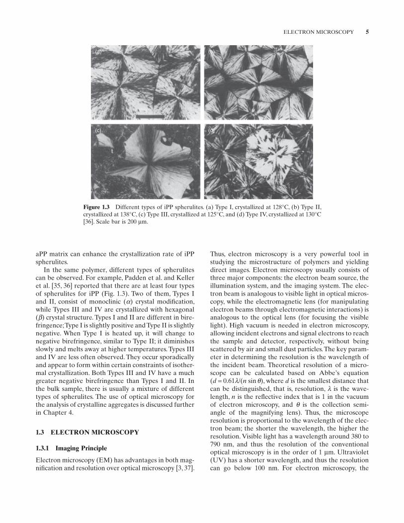
In the same polymer, different types of spherulites can be observed. For example, Padden et al. and Keller et al. [35, 36] reported that there are at least four types of spherulites for iPP (Fig. 1.3). Two of them, Types I and II, consist of monoclinic (α) crystal modification, while Types III and IV are crystallized with hexagonal (β) crystal structure. Types I and II are different in birefringence; Type I is slightly positive and Type II is slightly negative. When Type I is heated up, it will change to negative birefringence, similar to Type II; it diminishes slowly and melts away at higher temperatures. Types III and IV are less often observed. They occur sporadically and appear to form within certain constraints of isothermal crystallization. Both Types III and IV have a much greater negative birefringence than Types I and II. In the bulk sample, there is usually a mixture of different types of spherulites. The use of optical microscopy for the analysis of crystalline aggregates is discussed further in Chapter 4.
1.3 ELECTRON MICROSCOPY
1.3.1 Imaging Principle
Electron microscopy (EM) has advantages in both magnification and resolution over optical microscopy [3, 37].
Figure 1.3 Different types of iPP spherulites. (a) Type I, crystallized at 128°C, (b) Type II, crystallized at 138°C, (c) Type III, crystallized at 125°C, and (d) Type IV, crystallized at 130°C [36]. Scale bar is 200 μm.
(a) (b)
(c) (d)
6 EXPERIMENTAL TEChNIquES
and the atoms in the sample, where coherent backward scattered (about 180°) electrons are formed. Their intensity is thus related to the atomic number—higher mass atom leads to more backscattered electrons and brighter appearance in the image. The secondary electrons result from the electrons that gain energy by inelastic collision between the sample and the incident beam. Due to the restriction of low energy (usually below 50 eV), only secondary electrons escaping near the surface can be detected. Thus, these signals can provide information on the surface topology. After the emission of secondary electrons, higher energy electrons within the atoms can fall into the vacant orbital at the lower energy level, thus generating characteristic Xrays that can also be collected to determine the surface composition. The modern SEM technique can be combined with in situ sample stages to investigate realtime behavior of a sample under micromechanical and electrically stimulated environments.
1.3.2 Sample Preparation
1.3.2.1 Thin-Film Preparation SEM requires relatively simple procedures for sample preparation. The samples can be in the form of fiber, film, or bulk, as long as they can be mounted on the sample stub (e.g., using the doublesided carbon tape). however, TEM requires the sample to be ultrathin, usually less than 100 nm, which allows electron beams to go through. For large samples, ultramicrotomy can be used to yield an ultrathin film. For solution and particles, dispersion, casting, and disintegration onto the metal grid with an electron transparent support film are good choices. In addition, sample replication (an indirect method) can also be used to prepare ultrathin specimens. This method involves the evaporation of replicating media, such as carbon or metals, on the sample surface in vacuum to form an ultrathin film. The original sample is subsequently removed (dissolved chemically or physically), leaving the replica with the same surface characteristic and topography of the original sample. For samples that cannot be easily removed, twostage replication can be used. The first step involves the use an easily removable material, such as poly(acrylic acid) (PAA), followed by the conventional replication step to fabricate the ultrathin specimen for TEM observation.
1.3.2.2 Conducting Problem Since most polymers are nonconductive, when high energy electron beams are illuminated on the sample surface, the surface charge will accumulate and damage the sample. To prevent the accumulation of electrostatic charge on the surface, it is necessary to coat the sample with electronconducting materials, such as gold. But it has to be sufficiently thin
wavelength of the electron beam is much shorter than visible light, so a much higher resolution can be achieved. The wavelength of electron beam is related to the accelerating voltage (λ = h/[2m0eV(1 + eV/2m0c2)]1/2); a higher voltage can result in a shorter wavelength, leading to a better resolution. For instance, with a voltage of 100 kV, the wavelength of the electron beam is 0.0037 nm, yielding a theoretical resolution of 0.005 nm. however, because of the limitation of many other factors, such as monochromation and focusing, the theoretical resolution cannot be obtained. A typical practical limit of resolution for electron microscopy is in the order of 1 nm.
1.3.1.1 Transmission Electron Microscopy When light goes through a thin sample, a different thickness or different density component in the sample would lead to different absorption of light, thus forming an optical image. however, the image formation in transmission electron microscopy (TEM) is due to scattering of electrons rather than absorption of light [38, 39]. Thicker regions or regions with a higher atomic mass would result in stronger scattering, enabling the region to appear darker in the reconstructed image (this is because more incident electrons are scattered to larger angles). Based on this principle, there are two basic modes in TEM operation: brightfield mode and darkfield mode. In the brightfield mode, the direct transmitted electron beam is collected to construct the image; in the darkfield mode, the diffracted electron beam is used. Such an operation is accomplished by inserting an aperture into the back focal plane of the objective lens and moving the aperture around to let the relative electron beam, that is, transmitted beam or scattered beam, pass through. Since diffracted beams can strongly interact with samples possessing planar defects, stacking faults or particles, the operation of darkfield mode is preferred. In contrast, when interactions between the electron beam and sample are relatively weak, the sample thickness and atomic mass and crystalline region will be more relevant to construct the image using the brightfield mode.
1.3.1.2 Scanning Electron Microscopy The major difference between scanning electron microscopy (SEM) and TEM is that in the former, electron beams are scanned over a region of the sample surface. When electron beams interact with the sample in a depth of a few to hundreds of nanometers, a variety of backward detectable signals can be collected, including secondary electrons, backscattered electrons, Xrays, and so on. [40, 41]. Each of them can be used to characterize the sample with respect to different properties. The backscattered electrons result from the collision of incident electrons
ELECTRON MICROSCOPy 7
of 10 torr is maintained in the sample chamber). The incident electron beam still passes through a high vacuum column along most of its path, maintained by using pressurelimiting apertures and separating pumps. The distance between the final aperture and the sample surface is around a few millimeters, allowing the reduction of scattering by gas molecules and yielding a high resolution image. The detector is also modified to collect signals under mild environment in the sample chamber. Since ESEM can be operated without coating and under gas environment, many other applications for semicrystalline polymers can be carried out, for example, the melt processing of polymers and liquid–solid interface reaction.
1.3.3.2 High Resolution SEM high resolution SEM is developed by exchanging the regular tungsten filament electron gun with a fieldemission gun [42]. The rationale is as follows. It is known that the percentage of SE1 (the direct emitted secondary electrons closed to the sample surface) in the total secondary electrons, including SE2, SE3 (from backscattered electrons, which lose most of their energy when they escape from the sample or hit the wall of the chamber), and SE4 (produced in the electron column), determines the spatial resolution of the image, whereby this percentage is limited by the diameter of the electron probe. The fieldemission gun is suitable for high resolution purposes because its probe size is very small (about 1 nm). In addition, the working distance can be short (e.g., a few millimeters), which can enhance the spatial resolution due to low spherical and chromatic aberration.
high resolution TEM (hRTEM) lattice images can be obtained by collecting both transmitted and scattered beams using a large objective aperture. Images are formed from the interference between the beams, giving information regarding lattice parameters, defects and orientation, and so on. In order to achieve high resolution, both high image contrast and high instrumental resolution power are needed. usually, this requires that the spherical and chromatic aberration and electron wavelength to be as small as possible. Thus, high voltage is needed to generate incident electron beams with high energy and short wavelength. Advanced hRTEM is usually operated at 300 kV and above. Best resolution in the range of 0.5 Å can be achieved. Chromatic aberration can be improved by applying electron velocity filters, in which the electrons with different energies are sorted out, leaving only monochromatic electrons; spherical aberration can be minimized by changing the setup of the lens design. Additionally, other instrumentation parameters, such as beam divergence, magnification, and radiation sensitivity (especially for polymers), also need to be optimized to achieve high resolution.
without disturbing the surface structure of the sample. The common coating techniques include sputter coating and vacuum evaporation. Sputter coating is fast and convenient, but it is usually used for low magnification. The vacuum evaporation method gives finer grains and thinner conductive coating, which is more suitable for high resolution imaging. For TEM observation, samples are usually metal shadowed at an oblique angle (20° to 45°). Since the heavy atoms have strong scattering ability, regions without these metal coatings appear darker in the image. Thus, it can be used to highlight the surface topology and enhance the electron contrast.
1.3.2.3 Contrast Problem The contrast formation in TEM arises from interactions between incident electrons and atoms. The contrast of a polymer sample is often low. This is because polymers usually consist of light atoms such as C, O, and h with only small variations in electron density. To increase the contrast, chemical staining or etching can be applied. Chemical staining involves the incorporation of heavy elements into the sample by chemical reaction. Physical staining is used relatively less often, as it is often not stable in the vacuum environment. Several staining agents (e.g., osmium tetroxide, ruthenium tetroxide, and chlorosulfonic acid, phosphotungstic acid) have been demonstrated, depending on the structure of the sample (especially the functional group). Shadowing with heavy metal atoms can also enhance the contrast. Chemical or physical etching methods are other ways to enhance the surface structure. Chemical etching involves the use of chemical solvent (e.g., acid) to etch away some nonessential part of the sample surface (e.g., amorphous region) to enhance the essential part of the structure (e.g., crystalline region), followed by making replicas or conductive coatings. Physical etching involves the use of plasma or ion beam to etch the sample surface; however, the technique is known to produce artifacts in semicrystalline polymers.
1.3.3 Relevant Experimental Techniques
1.3.3.1 Environmental SEM In conventional SEM, nonconductive polymer samples need be surface coated, whereby the original surface morphology can be damaged or distorted. Environmental SEM (ESEM) is a new technique that allows wet or insulating samples, such as polymers, biological cells, and plants without any pretreatment, to be studied under low pressure and high humidity environments. The charge accumulation problem is resolved by neutralizing negative charges on the sample surface with positively charged ions generated by the interaction between electron beams and surrounding gas molecules (a gas pressure on the order
8 EXPERIMENTAL TEChNIquES
1.3.4 Selected Applications
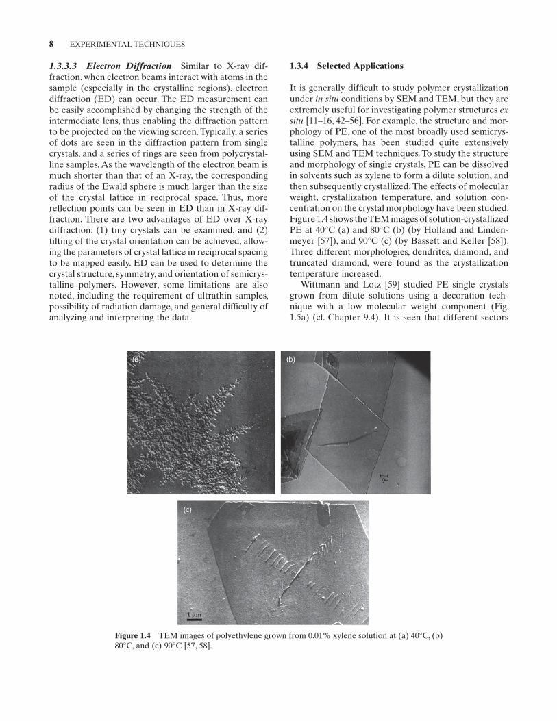
It is generally difficult to study polymer crystallization under in situ conditions by SEM and TEM, but they are extremely useful for investigating polymer structures ex situ [11–16, 42–56]. For example, the structure and morphology of PE, one of the most broadly used semicrystalline polymers, has been studied quite extensively using SEM and TEM techniques. To study the structure and morphology of single crystals, PE can be dissolved in solvents such as xylene to form a dilute solution, and then subsequently crystallized. The effects of molecular weight, crystallization temperature, and solution concentration on the crystal morphology have been studied. Figure 1.4 shows the TEM images of solutioncrystallized PE at 40°C (a) and 80°C (b) (by holland and Lindenmeyer [57]), and 90°C (c) (by Bassett and Keller [58]). Three different morphologies, dendrites, diamond, and truncated diamond, were found as the crystallization temperature increased.
Wittmann and Lotz [59] studied PE single crystals grown from dilute solutions using a decoration technique with a low molecular weight component (Fig. 1.5a) (cf. Chapter 9.4). It is seen that different sectors
1.3.3.3 Electron Diffraction Similar to Xray diffraction, when electron beams interact with atoms in the sample (especially in the crystalline regions), electron diffraction (ED) can occur. The ED measurement can be easily accomplished by changing the strength of the intermediate lens, thus enabling the diffraction pattern to be projected on the viewing screen. Typically, a series of dots are seen in the diffraction pattern from single crystals, and a series of rings are seen from polycrystalline samples. As the wavelength of the electron beam is much shorter than that of an Xray, the corresponding radius of the Ewald sphere is much larger than the size of the crystal lattice in reciprocal space. Thus, more reflection points can be seen in ED than in Xray diffraction. There are two advantages of ED over Xray diffraction: (1) tiny crystals can be examined, and (2) tilting of the crystal orientation can be achieved, allowing the parameters of crystal lattice in reciprocal spacing to be mapped easily. ED can be used to determine the crystal structure, symmetry, and orientation of semicrystalline polymers. however, some limitations are also noted, including the requirement of ultrathin samples, possibility of radiation damage, and general difficulty of analyzing and interpreting the data.
Figure 1.4 TEM images of polyethylene grown from 0.01% xylene solution at (a) 40°C, (b) 80°C, and (c) 90°C [57, 58].
(a) (b)
(c)

ATOMIC FORCE MICROSCOPy 9
the adjacent lamellar kebabs of similar size and crystal habit (Fig. 1.6). This phenomenon is discussed further in Chapter 15.
1.4 ATOMIC FORCE MICROSCOPY
1.4.1 Imaging Principle
Atomic force microscopy (AFM) works by scanning the sample surface using a sharp and tiny probe, which is mounted at the end of a cantilever [61, 62]. When the AFM probe scans the sample surface, the interaction forces (including mechanical contact force, electrostatic force, and van der Waals force) between the probe and the sample induce deflection of the cantilever. This deflection can be detected by the change of position of a laser beam reflected on the back of a cantilever and into a positionsensitive detector. Based on this principle, an image of sample surface can be generated. The cantilever is several hundred micrometers long, while the radius of the probe tip is from a few to tens of nanometers. The sharpness, aspect ratio, and the shape of the probe are the most critical parameters to the resolution of AFM. Generally, the sharper probe leads to higher resolution in the image.
1.4.2 Scanning Modes
There are two major scanning modes in AFM: contact mode and vibration mode. In the contact mode, the probe is in contact with the sample surface, where an interaction force is generated. This mode is usually used when the sample surface is hard. To protect the probe and cantilever from colliding with the sample, the cantilever deflection is controlled and adjusted to a fixed
Figure 1.5 (a) TEM image of polyethylene single crystal, decorated by vacuum deposition of low molecular weight polyethylene, grown from dilute solution. Scale bar = 1 μm. Electron diffraction patterns of a single polyethylene crystal from an area encompassing (b) all four and (c) only one (lower right or upper left region in (a)) growth sector [59].
(a)
(b) (c) Figure 1.6 SEM image of tolueneextracted uhMWPE crystallites with a shish–kebab structure having multiple shish [60].
have different preferred orientations. Two ED patterns taken on regions encompassing all four sectors and only one sector (lower right or upper left of Fig. 1.5a) are illustrated in Figure 1.5b,c, respectively. In Figure 1.5c, the caxis orientation of the decorating chains is parallel to the growth face in the selected area (the arrow indicates the 110 spot). The orientations of the lamellar rods and polymer chains are thus confirmed to be perpendicular and parallel, respectively, to the growth front of the corresponding sector.
It is well known that flowinduced crystallization of polymers can lead to shish–kebab structure. hsiao et al. [60] extracted the ultrahigh molecular weight PE (uhMWPE) shish–kebab entities crystallized after shear cession from the low molecular weight PE matrix at a temperature between the melting points of the two. The shish–kebab crystals were examined with a fieldemission SEM at the accelerating voltage of 2 kV. Figure 1.6 shows that multiple shish are formed, where each shish has a diameter of a few nanometers and connects
10 EXPERIMENTAL TEChNIquES
sample surface and obtain an image. The scanning time is simply not fast enough to yield realtime information about polymer crystallization or melting processes, whose rate is about 1–2 orders of magnitude faster than the imaging speed. A new video AFM [64] technique has been developed, where the imaging speed is in the range of tens of milliseconds. This technique is ideal for studying many kinetics/dynamics behaviors of crystalline polymers in real time. The principle of this technique is that when a force is applied to the end of the tip, the responding resonance of the cantilever (the source of limitation in the scanning rate) is changed. As a result, the imaging rate is significantly improved.
1.4.5 Selected Applications
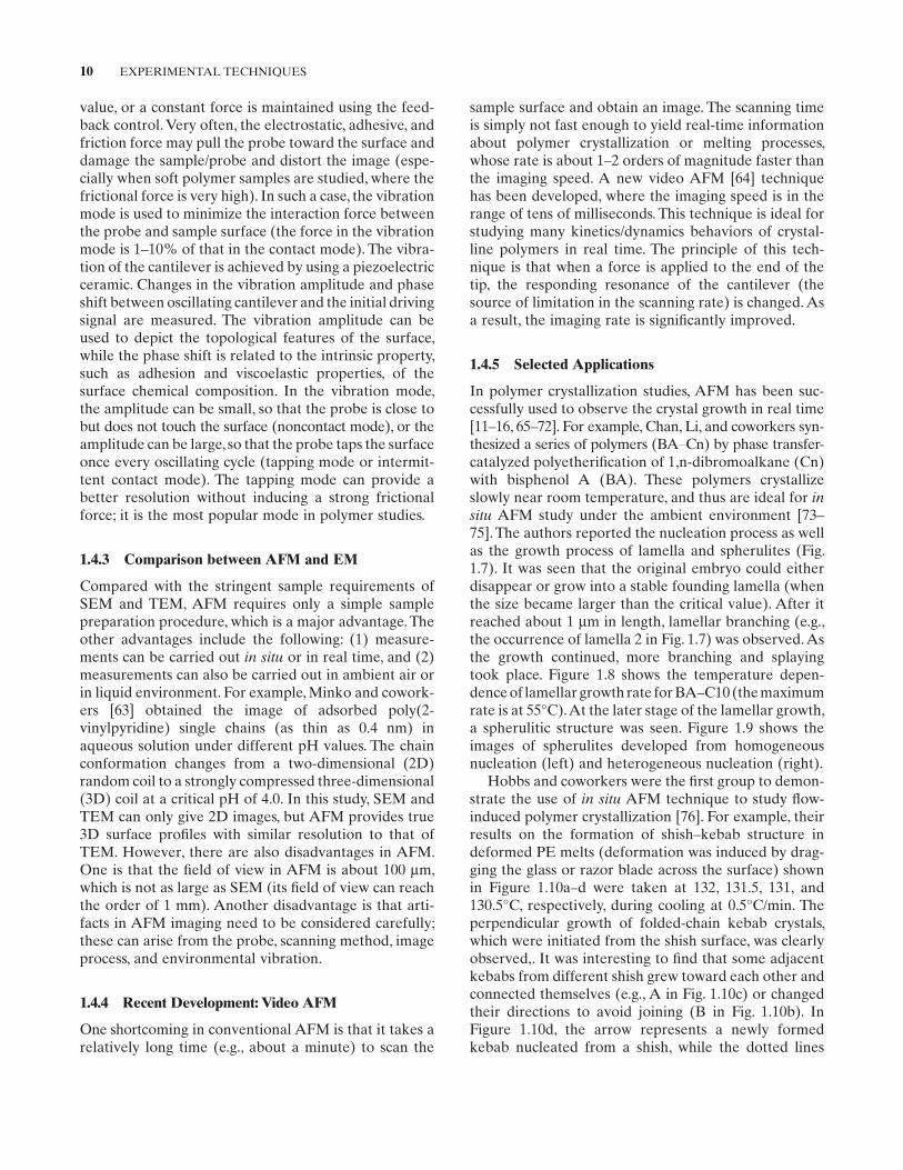
In polymer crystallization studies, AFM has been successfully used to observe the crystal growth in real time [11–16, 65–72]. For example, Chan, Li, and coworkers synthesized a series of polymers (BA–Cn) by phase transfercatalyzed polyetherification of 1,ndibromoalkane (Cn) with bisphenol A (BA). These polymers crystallize slowly near room temperature, and thus are ideal for in situ AFM study under the ambient environment [73–75]. The authors reported the nucleation process as well as the growth process of lamella and spherulites (Fig. 1.7). It was seen that the original embryo could either disappear or grow into a stable founding lamella (when the size became larger than the critical value). After it reached about 1 μm in length, lamellar branching (e.g., the occurrence of lamella 2 in Fig. 1.7) was observed. As the growth continued, more branching and splaying took place. Figure 1.8 shows the temperature dependence of lamellar growth rate for BA–C10 (the maximum rate is at 55°C). At the later stage of the lamellar growth, a spherulitic structure was seen. Figure 1.9 shows the images of spherulites developed from homogeneous nucleation (left) and heterogeneous nucleation (right).
hobbs and coworkers were the first group to demonstrate the use of in situ AFM technique to study flowinduced polymer crystallization [76]. For example, their results on the formation of shish–kebab structure in deformed PE melts (deformation was induced by dragging the glass or razor blade across the surface) shown in Figure 1.10a–d were taken at 132, 131.5, 131, and 130.5°C, respectively, during cooling at 0.5°C/min. The perpendicular growth of foldedchain kebab crystals, which were initiated from the shish surface, was clearly observed,. It was interesting to find that some adjacent kebabs from different shish grew toward each other and connected themselves (e.g., A in Fig. 1.10c) or changed their directions to avoid joining (B in Fig. 1.10b). In Figure 1.10d, the arrow represents a newly formed kebab nucleated from a shish, while the dotted lines
value, or a constant force is maintained using the feedback control. Very often, the electrostatic, adhesive, and friction force may pull the probe toward the surface and damage the sample/probe and distort the image (especially when soft polymer samples are studied, where the frictional force is very high). In such a case, the vibration mode is used to minimize the interaction force between the probe and sample surface (the force in the vibration mode is 1–10% of that in the contact mode). The vibration of the cantilever is achieved by using a piezoelectric ceramic. Changes in the vibration amplitude and phase shift between oscillating cantilever and the initial driving signal are measured. The vibration amplitude can be used to depict the topological features of the surface, while the phase shift is related to the intrinsic property, such as adhesion and viscoelastic properties, of the surface chemical composition. In the vibration mode, the amplitude can be small, so that the probe is close to but does not touch the surface (noncontact mode), or the amplitude can be large, so that the probe taps the surface once every oscillating cycle (tapping mode or intermittent contact mode). The tapping mode can provide a better resolution without inducing a strong frictional force; it is the most popular mode in polymer studies.
1.4.3 Comparison between AFM and EM
Compared with the stringent sample requirements of SEM and TEM, AFM requires only a simple sample preparation procedure, which is a major advantage. The other advantages include the following: (1) measurements can be carried out in situ or in real time, and (2) measurements can also be carried out in ambient air or in liquid environment. For example, Minko and coworkers [63] obtained the image of adsorbed poly(2vinylpyridine) single chains (as thin as 0.4 nm) in aqueous solution under different ph values. The chain conformation changes from a twodimensional (2D) random coil to a strongly compressed threedimensional (3D) coil at a critical ph of 4.0. In this study, SEM and TEM can only give 2D images, but AFM provides true 3D surface profiles with similar resolution to that of TEM. however, there are also disadvantages in AFM. One is that the field of view in AFM is about 100 μm, which is not as large as SEM (its field of view can reach the order of 1 mm). Another disadvantage is that artifacts in AFM imaging need to be considered carefully; these can arise from the probe, scanning method, image process, and environmental vibration.
1.4.4 Recent Development: Video AFM
One short coming in conventional AFM is that it takes a relatively long time (e.g., about a minute) to scan the

ATOMIC FORCE MICROSCOPy 11
Figure 1.7 AFM tapping mode images of BAC8 during crystallization at room temperature. One embryo developed into a straight founding lamella; later the branching and splaying occurred [73–75].
0.3μm
Figure 1.8 Lamellar growth rate of BAC10 as a function of crystallization temperature [73–75].
2.0
1.5
1.0
0.5
0.0
0 20 40
Lam
ella
r G
row
th R
ate
(nm
/s)
60
Temperature (°C)
80 100
Figure 1.9 AFM images of homogeneously nucleated (left) and heterogeneously nucleated (right) BAC8 spherulites crystallized at 30°C [73–75].
indicate the distorting effect of drift. The authors also measured the growth rate of individual lamellae (numbers 1–7 in Fig. 1.11) under isothermal conditions. They found that the growth rate of a chosen lamella varied significantly at different times, and they also varied for different lamellae at a specific time. This indicates that the constant growth rate of spherulites
observed by optical microscopy was not the case for lamellar structures at nanoscale. Further illustrations of this technique are discussed in Chapter 15.
Sophisticated numerical analysis on AFM images can be used to obtain lamellar information. Figure 1.12a–c represents AFM phase images showing the evolution of crystalline structure of PCL/PVC 75/25 (wt/wt) blend at 40°C by Ivanov et al. [77, 78]. Since the boundary between crystal and amorphous phases was defined more clearly in phase image than height image, they chose a critical value in phase image, which was obtained by optimizing the contour line fuzziness, to represent

12 EXPERIMENTAL TEChNIquES
poly(ethylene terephthalate) (PET) and its distribution during crystallization at 233°C, as shown in Figure 1.13. The thickness of the PET lamella was quite uniform, about 10 nm, without much variation as the time elapsed during isothermal crystallization.
1.5 NUCLEAR MAGNETIC RESONANCE
Nuclear magnetic resonance (NMR) is a powerful spectroscopic technique for studying semicrystalline polymers [79, 80]. The principle of NMR is based on the transition between quantized energy levels caused by the interactions between the material and electromagnetic radiation. There are some prerequisites for the materials suitable for NMR study. First, the nuclei should have a spin angular momentum with an associated magnetic moment, which means the spin quantum number (I) of the nuclei cannot be zero. This requires an odd number of protons or neutrons in the nuclei. Nuclei like 16O or 12C are thus not applicable in NMR spectroscopy. Second, an external magnetic field B0 is needed to induce the split of the energy levels, depending on the direction of spin component: parallel or antiparallel to B0. The number of energy levels is given by 2I + 1. Thus, nuclei like 1h and 13C (whose I is 1/2) have two energy levels; for other nuclei with I value of 1 or
Figure 1.12 (a), (b), (c) are 1 × 1 μm2 AFM phase images recorded during isothermal melt crystallization of a PCL/PVC 75/25 (wt/wt) blend at 40°C. Elapsed times are 0 s (a), 541 s (b), and 2931 s (c). The full gray scale is 16°. (d) Volume crystallinity estimated from the images taken at the session [77, 78].
(a) (b)
(c)(d)
Time (s)
Cry
stal
linity
(vo
l/vol
)
0 2000
0.4
0.2
0.0
Figure 1.11 The growth rate of seven individual lamella (numbers 1–7) from isothermal crystallization of PE at various times [76].
1
00 2 4 6
Lamella
Gro
wth
rat
e (n
m/s
)
8
the intensity envelope of the boundary. So the phase image can be converted to binary format containing only crystal pixels and amorphous pixels, which were above or below the critical value, respectively. The volume crystallinity was estimated by the fraction of crystal pixels, and the results are illustrated in Figure 1.12d. They also obtained the crystal thickness of
Figure 1.10 A series of AFM phase images showing the growth of shish–kebab structure in deformed PE melts during cooling. The gray scale represents a change in the phase angle of 60°. The scale bar represents 300 nm [76].
(a) (b)
(c) (d)