hamache, abdelghani and sengouga, nouredine and …eprints.nottingham.ac.uk/39518/1/modelling the...
TRANSCRIPT
Hamache, Abdelghani and Sengouga, Nouredine and Meftah, Afak and Henini, Mohamed (2016) Modeling the effect of 1 MeV electron irradiation on the performance of n(+)-p-p(+) silicon space solar cells. Radiation Physics and Chemistry, 123 . pp. 103-108. ISSN 0969-806X
Access from the University of Nottingham repository: http://eprints.nottingham.ac.uk/39518/1/Modelling%20the%20effect%20of%201%20%20MeV%20electron%20irradiation%20%20on%20the%20performance%20of%20%20n%20-p-p%20%20Si%20space%20solar%20%20cells%201.pdf
Copyright and reuse:
The Nottingham ePrints service makes this work by researchers of the University of Nottingham available open access under the following conditions.
This article is made available under the Creative Commons Attribution Non-commercial No Derivatives licence and may be reused according to the conditions of the licence. For more details see: http://creativecommons.org/licenses/by-nc-nd/2.5/
A note on versions:
The version presented here may differ from the published version or from the version of record. If you wish to cite this item you are advised to consult the publisher’s version. Please see the repository url above for details on accessing the published version and note that access may require a subscription.
For more information, please contact [email protected]
Modeling the effect of 1 MeV electron irradiation on the performance of n+p-p
+ Silicon space
solar cells
Abdelghani Hammachea, Nouredine Sengouga
a,*, Afak Meftah
a, Mohamed Henini
b
a Laboratory of Metallic and Semiconducting Materials (LMSM), Université de Biskra, BP
455 RP, 07000 Biskra, Algeria.
b School of Physics and Astronomy, Nottingham Nanotechnology and Nanoscience Center,
University of Nottingham, Nottingham, NG7 2RD, UK
* Corresponding author [email protected] (N. Sengouga)
ABSTRACT
Energetic particles such as electrons and protons induce severe degradation on the
performance of solar cells used to power satellites and space vehicles. This degradation is
usually attributed to lattice damage in the active region of the solar cell. One of the
phenomena observed in silicon solar cells exposed to 1 MeV electron irradiation is the
anomalous degradation of the short circuit current (𝐽𝑆𝐶). It initially decreases followed by a
recovery before falling again with increasing electron fluence. This behavior is usually
attributed to type conversion of the solar cell active region. The other figures of merit, on the
other hand, decrease monolithically. In this work numerical simulator SCAPS (Solar Cell
Capacitance Simulator) is used to elucidate this phenomenon. The current-voltage (J-V)
characteristics of a Si n+-p-p
+ structure are calculated under AM0 with the fluence of 1MeV
electrons as a variable parameter. The effect of irradiation on the solar cell is simulated by a
set of defects of which the energy levels lie deep in energy gap of silicon. Although several
types of deep levels are induced by irradiation including deep donors (DD), deep acceptors
(DA) and/or generation-recombination centers (GRC), it was found that, only one of them
(the shallowest donor) is responsible for the anomalous degradation of 𝐽𝑆𝐶 . It will be also
shown, by calculating the free charge carrier profile in the active region, that this behavior is
not related to type conversion but to a widening of the space charge region.
Keywords: Si solar cells; 1 MeV electron irradiation; short circuit current; numerical
simulation; SCAPS.
1. Introduction
For satellites and space vehicles, the only source of energy is photovoltaic solar cells.
Materials that can be used to make solar cells for this purpose have to withstand harsh
conditions that include high temperatures and energetic particles. Only a few materials such
as Si and some III-V semiconductors and their alloys (GaAs, InP and GaInP) can meet these
conditions [1, 2]. Good quality crystals with well controlled doping can be easily achieved
due to the mature technology of these semiconductors. Compound semiconductors are
preferred because of their higher conversion efficiencies and radiation-resistance, but silicon
still has a better cost effectiveness and reliability. The solar cells used in space are subjected
to charged particles such as protons and electrons of a wide energy range. The highly
energetic particles interacting with solar cells induce defects in the semiconductor lattice and,
consequently, deteriorate the solar cell performance [3]. The performance degradation of solar
cells subjected to energetic electrons and protons in laboratories is well characterized [4-9]. It
was observed that the space solar figures of merit (the short circuit current 𝐼𝑆𝐶 , the open
circuit voltage 𝑉𝑂𝐶 , the maximum output power 𝑃𝑀𝐴𝑋 , the fill factor 𝐹𝐹 and the conversion
efficiency 𝜂) decrease linearly with the logarithm of the fluence. The degradation was
analytically modeled [10-14] in order to predict the effect of the long term exposure of the
solar cells [15, 16]. For example, 𝑃𝑀𝐴𝑋 is related to the irradiation fluence by a simple
formula of the form [17]:
𝑃𝑀𝐴𝑋 𝜑 = 𝑃0 1 − 𝐶ln𝜑
𝜑0 (1)
where 𝜑 is the irradiation fluence, 𝜑0 is the fluence threshold for the power reduction, 𝑃0 is
the pre-irradiated maximum output power and 𝐶 is a fitting constant. The other figures of
merit follow a similar pattern, in most cases, which means that they decrease monolithically
with increasing fluence. However, in some silicon solar cells, the short circuit current does not
strictly follow this behavior. Instead, it initially decreases, then at a certain fluence it slightly
increases before decreasing again sharply [2, 5, 7, 9, 13-14, 18-19]. This slight recovery of the
short circuit current is usually attributed to a type conversion of the base (from n to p-type for
example) [20]. Among the defects created by irradiation are compensating centers which

reduce the initial doping density. They are responsible of a phenomenon known as carrier
removal, which is modeled by an analytical expression [14] expressed by:
𝑝𝜑 = 𝑝0𝑒𝑥𝑝 −𝑅𝐶𝜑
𝑝0 (2)
𝑝0 is the initial hole density (post-irradiated p-type Si) and 𝑅𝐶 is the removal rate.
The analytical modeling of the anomalous degradation of the short circuit current divides the
𝐼𝑆𝐶 𝜑 curve into four regions [2, 5, 7, 14, 18]. The first region is just for 𝜑 < 𝜑0, i.e. when
𝐼𝑆𝐶 is still not affected by 𝜑. In this region the created defects have negligible densities
compared to shallow doping. The second region is when the short circuit decreases with
increasing fluence. This is explained by a decrease in the minority carrier lifetime and hence
in their diffusion length. The dependence of 𝐼𝑆𝐶 on the diffusion length 𝐿 and the space
charge region width 𝑊 is roughly given by:
𝐼𝑆𝐶 = 𝑞𝐹 1 − exp(−𝛼𝑊) 1 + 𝛼𝐿 (3)
𝛼 is the absorption coefficient and 𝐹 is the photon flux.
The third region is when the short circuit increases with increasing fluence. This is related to
the onset of the type conversion where the space charge width increases instead of decreasing.
Therefore the short circuit current increases according to equation (3). The fourth region is
when the short circuit falls sharply with increasing fluence. This is explained by the increase
in the base resistivity associated with the decrease in carrier concentration due to
compensation by deep defects. Another work by Karazhanov [13] assumed a simplified model
in which the free carriers (holes) are compensated by a single donor deep level. The
conversion of the p-type semiconductor to n-type is reached when the deep level
concentration surpasses that of holes. This leads to an increase in the short circuit current, also
according to equation (3).
In the above analysis several simplifications were made. In particular, the defects created by
irradiation are assumed to act as one effective deep level. In reality and as it is well known,
irradiation creates several defects of different types: GRCs, DDs and DAs [21-26].
Experimentally it is not always easy to distinguish GRs from DDs and DAs. This means that
analytical modeling cannot clearly link the observed degradation of the solar cell figures of
merit to a particular defect. On the other hand numerical simulation has the ability of
unequivocally relating the degradation of each figure of merit to a particular defect [27-33]. In
the present work, it can reveal which defect is responsible for the observed phenomenon (the
anomalous behavior of the short circuit current) in Si solar cells. It can also evaluate the
behavior of internal parameters such as the free carrier concentration so that they can be used
to explain the observed effect. Numerical simulation is carried out using the software SCAPS
(Solar Cell Capacitance Simulator) developed by M. Burgelman and co-workers at the
Department of Electronics and Information Systems (ELIS) of the University of Gent,
Belgium [34].
2. Simulation
The current-voltage characteristics of the solar cell are calculated using the software SCAPS.
SCAPS is a Windows application program, organized in a number of panels, in which the user
can set the parameters. The program opens with an `action panel', where the user can set an
operating point (temperature, voltage, frequency, illumination), and an action list of
calculations to carry out (J-V, C-V, C-f, Q(λ )). In each calculation, the running parameter (V,
f or λ) is varied in the specified range, whilst all other parameters have the values specified in
the operation point. Also, the user can directly view previously calculated results, namely J-
V, C-V, C-f, Q(λ), and also band diagrams, electric field, carrier densities, partial
recombination currents.
Like any numerical simulation, SCAPS solves the basic semiconductor equations which are:
the Poisson equation, relating the charge to the electrostatic potential 𝜓, and the continuity
equations for electrons and holes. In one dimension, the total cell length L is divided into N
intervals, and the value of 𝜓𝑖 and the electron and hole concentrations 𝑛𝑖 and 𝑝𝑖 at each of the
intervals constitute the unknowns of the problem. They can be found by numerically solving
3N non-linear equations, i.e. the basic equations at each of the intervals i. Alternatively, one
can choose 𝜓𝑖 , 𝜙𝑛 and 𝜙𝑝 as independent variables instead of (𝜓𝑖 , 𝑛𝑖 , 𝑝𝑖). Here 𝜙𝑛 and 𝜙𝑝 are
the quasi-fermi energy levels for electrons and holes respectively. The basic equations are
non-linear because the continuity equations contain a recombination term, which is non-linear
in 𝑛 and 𝑝.
The simplest and useful model of charge transport is the Drift-Diffusion Model. This model,
which is based on the two first equations cited above, is adequate for nearly all devices that
were technologically feasible. The Poisson's equation which relates the electrostatic potential
to the space charge density is given by:

𝜀𝑑2𝜓
𝑑𝑥2 = −𝜌 𝑥 (4)
where 𝜓 is the electrostatic potential, 𝜀 is the local permittivity, and 𝜌 is the local space
charge density.
The continuity equations in steady state for electrons and holes are expressed, respectively by:
0 =1
𝑞
𝑑𝐽𝑛
𝑑𝑥+ 𝐺𝑛 − 𝑅𝑛 (5.a)
0 = −1
𝑞
𝑑𝐽𝑝
𝑑𝑥+ 𝐺𝑝 − 𝑅𝑝 (5.b)
where 𝑛 and 𝑝 are the electron and hole concentration, 𝐽𝑛 and 𝐽𝑝 are the electron and hole
current densities, 𝐺𝑛 and 𝐺𝑝 are the generation rates for electrons and holes, 𝑅𝑛 and 𝑅𝑝 are the
recombination rates for electrons and holes, and 𝑞 is the electron charge.
In the drift-diffusion model, the current densities are expressed in terms of the quasi-Fermi
levels 𝜙𝑛 and 𝜙𝑝 as:
𝐽 𝑛 = −𝑞𝜇𝑛𝑛d𝜙𝑛
dx (6.a)
𝐽 𝑝 = −𝑞𝜇𝑝𝑝d𝜙𝑝
dx (6.b)
where 𝜇𝑛 and 𝜇𝑝 are the electron and hole mobilities, respectively. The quasi-Fermi levels are
linked to the carrier concentrations and the potential through the two Boltzmann
approximations:
𝑛 = 𝑛𝑖𝑒𝑥𝑝 𝜓−𝜙𝑛
𝑘𝐵𝑇 (7.a)
𝑝 = 𝑛𝑖𝑒𝑥𝑝 −𝜓−𝜙𝑝
𝑘𝐵𝑇 (7.b)
where 𝑛𝑖 is the effective intrinsic concentration and 𝑇 is the lattice temperature.
The electrical characteristics are calculated following the specified physical structure and bias
conditions. This is achieved by approximating the operation of the device into a one-
dimensional grid, consisting of a number of grid points called nodes. By applying the set of
differential equations (Poisson's and continuity equations) onto this grid (or equation's

discretization), the transport of carriers through the structure can be simulated. The finite
element grid is used to represent the simulation domain.
The Si solar cell used in this work is similar to that of [35]. It is a typical 50 µm thick n+-p-p
+
structure used for space applications. The different parameters of this solar cell are presented
in Table 1. A two-dimensional schematic view of the solar cell is shown in Fig. 1.
Table 1. The parameters of the Si n+-p-p+ solar cell simulated in this work.
Thickness (µm) Doping density (cm-3
) Type
Emitter 0.15 1 × 10¹⁹ n+
Base 49.70 1 × 10¹⁵ P
Back surface field region 0.15 5 × 10¹⁸ p+
Fig. 1. A two-dimensional schematic view of the Si n+-p-p
+ solar cell. BSF is the back surface
field.
The emitter side of the solar cell (n+) is illuminated by AM0 spectrum and the J-V
characteristics are calculated for different fluences of 1MeV electrons. Irradiation by these
energetic particles creates defects in the Si lattice, which manifest as recombination centers or
traps for free carriers. A lot of work is carried out to characterize these defects so that a large
number of defects are detected in Si. For simplicity we have used the most common observed
defects [1, 18]. These are summarized in Table 2.
Table 2. The parameters of the commonly detected defects in Si solar cells irradiated by 1 MeV
electrons [1, 18]. Introduction rate, k is the proportionality factor between the trap density and
the fluence (𝒌 = 𝑵𝑻/𝝋).

Activation energy
(eV)
Capture cross section, σ
(cm2)
Introduction rate, k
(cm-1
)
Trap type
𝐸𝑉 + 0.18 3.1 × 10⁻¹⁵ 0.002 Majority
𝐸𝑉 + 0.36 6.2 × 10⁻¹⁵ 0.016 Majority
𝐸𝐶 − 0.20 9.9 × 10⁻¹⁵ 0.002 Minority
𝐸𝑉 + 0.56 6.3 × 10⁻¹³ 0.004 Majority
𝐸𝐶 − 0.71 3.55 × 10⁻¹³ 0.004 Minority
3. Results and discussions
Since the solar cell used in this work has an n+-p-p
+ structure, it is expected that the defects
will be mainly created within the thickest region which is the p-type base where the majority
traps are hole traps while electron traps are the minority traps. Hence the majority traps will
only contribute to the reduction of the minority carrier lifetime but not to the shallow doping
compensation. It is therefore the minority traps which will be responsible for this
phenomenon. Referring to Table 2, there are only two minority traps: 𝐸𝐶 − 0.20 and 𝐸𝐶 −
0.71 𝑒𝑉. The second, the deepest, is only observed when the electron irradiation fluence
surpasses the critical value where the short circuit current shows the anomalous behavior. In
order to establish which trap is responsible the J-V characteristics are calculated under the
effect of each minority (donor-like) trap. Obviously, the majority traps are all taken into
account in both cases. It has to be also mentioned that, in numerical simulation, several
possibilities may be considered: the two minority traps are considered separately, then
together and in each case the trap parameters are adjusted to reproduce the experimental
behavior.
First when the two traps are taken individually with their parameters given in Table 2 and
then together, the calculated J-V characteristics under different fluences are shown in Fig. 2 a,
b and c for the shallower, 𝐸𝐶 − 0.20 𝑒𝑉, the deeper, 𝐸𝐶 − 0.71 𝑒𝑉, traps and together,
respectively.

Fig. 2. The calculated J-V characteristics of the n+-p-p
+ Si solar cell under AM0 for different
fluences of 1 MeV electron irradiation taking into account the majority traps with the minority
traps individually: (a) the shallower minority trap, 𝑬𝑪 − 𝟎.𝟐𝟎 𝒆𝑽; (b) the deeper minority trap,
𝑬𝑪 − 𝟎.𝟕𝟏 𝒆𝑽; and (c) the two minority traps together.
From these characteristics, the figures of merit of solar cell are extracted. The remaining
parameters after irradiation (normalized to their initial pre-irradiated values) are shown in Fig.
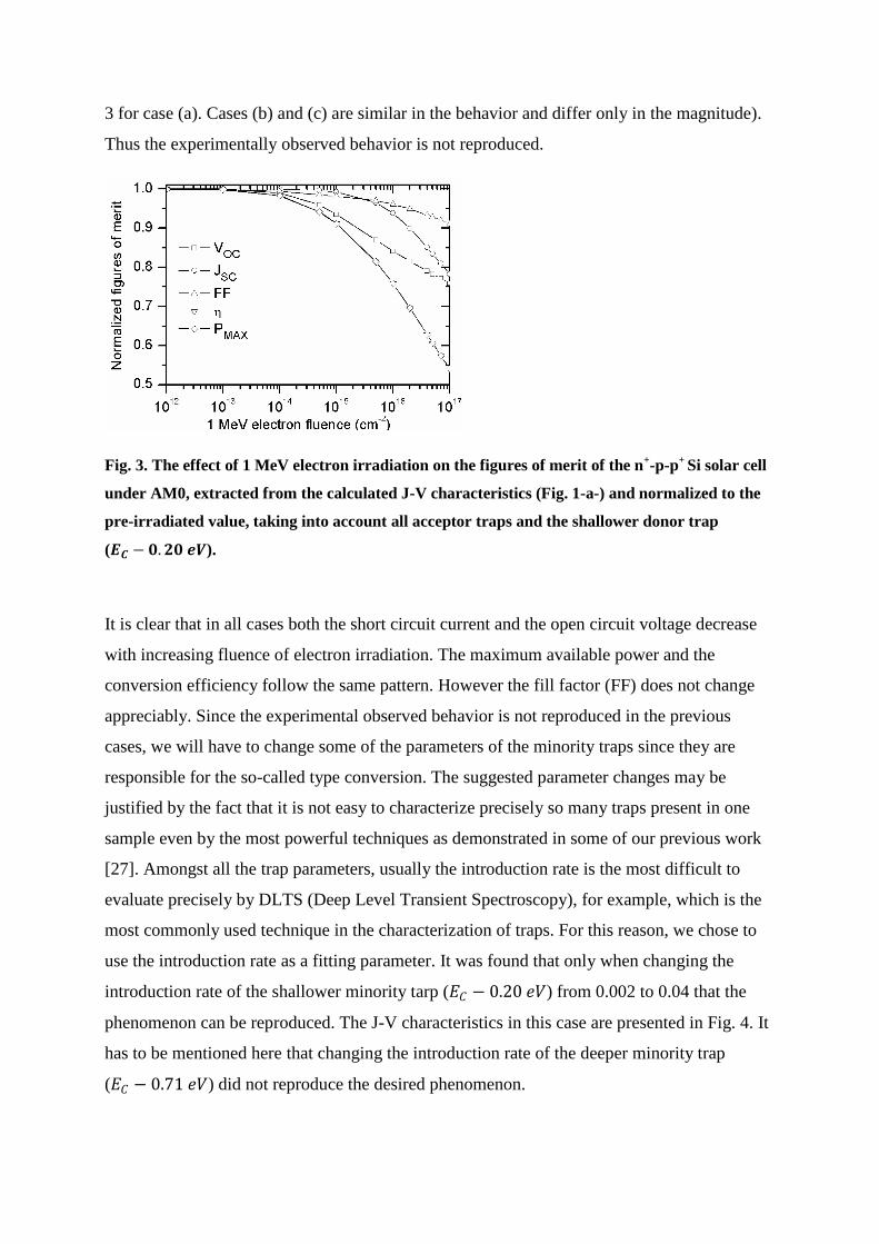
3 for case (a). Cases (b) and (c) are similar in the behavior and differ only in the magnitude).
Thus the experimentally observed behavior is not reproduced.
Fig. 3. The effect of 1 MeV electron irradiation on the figures of merit of the n+-p-p
+ Si solar cell
under AM0, extracted from the calculated J-V characteristics (Fig. 1-a-) and normalized to the
pre-irradiated value, taking into account all acceptor traps and the shallower donor trap
(𝑬𝑪 − 𝟎.𝟐𝟎 𝒆𝑽).
It is clear that in all cases both the short circuit current and the open circuit voltage decrease
with increasing fluence of electron irradiation. The maximum available power and the
conversion efficiency follow the same pattern. However the fill factor (FF) does not change
appreciably. Since the experimental observed behavior is not reproduced in the previous
cases, we will have to change some of the parameters of the minority traps since they are
responsible for the so-called type conversion. The suggested parameter changes may be
justified by the fact that it is not easy to characterize precisely so many traps present in one
sample even by the most powerful techniques as demonstrated in some of our previous work
[27]. Amongst all the trap parameters, usually the introduction rate is the most difficult to
evaluate precisely by DLTS (Deep Level Transient Spectroscopy), for example, which is the
most commonly used technique in the characterization of traps. For this reason, we chose to
use the introduction rate as a fitting parameter. It was found that only when changing the
introduction rate of the shallower minority tarp (𝐸𝐶 − 0.20 𝑒𝑉) from 0.002 to 0.04 that the
phenomenon can be reproduced. The J-V characteristics in this case are presented in Fig. 4. It
has to be mentioned here that changing the introduction rate of the deeper minority trap
(𝐸𝐶 − 0.71 𝑒𝑉) did not reproduce the desired phenomenon.

Fig. 4. The calculated J-V characteristics of the n+-p-p
+ Si solar cell under AM0 for different
fluences of 1 MeV electron irradiation by changing the introduction rate of the shallower
minority tarp (𝑬𝑪 − 𝟎.𝟐𝟎 𝒆𝑽) from 0.002 to 0.04 but excluding the deeper minority trap
(𝑬𝑪 − 𝟎.𝟕𝟏 𝒆𝑽).
It is very clear that there is a big difference as compared with the J-V characteristics shown in
Fig. 2. There are two main differences. First the fill factor is hugely affected in contrast to the
previous case. Second, the other figures of merit all decrease monolithically with increasing
electron fluence except the short circuit current which decreases then increases at a certain
fluence before it decreases abruptly again . To see this phenomenon even clearly, the short
circuit current is extracted from the J-V characteristics. It is then normalized to the un-
irradiated value and is presented in Fig. 5.
Fig.5 . The extracted short circuit current, normalized to the unirradiated value, from the
calculated J-V characteristics (Fig. 4) of the n+-p-p
+ Si solar cell under AM0 for different
fluences of 1 MeV electron irradiation by changing the introduction rate of the shallower

minority tarp (𝑬𝑪 − 𝟎.𝟐𝟎 𝒆𝑽) from 𝟎.𝟎𝟎𝟐 to 𝟎.𝟎𝟒 but excluding the deeper minority trap
(𝑬𝑪 − 𝟎.𝟕𝟏 𝒆𝑽).
Although the shape of the experimentally observed phenomenon is reproduced but the
steepness of its degradation is not. In fact the short circuit degradation is less than 10 %
before the appearance of the anomalous phenomenon. The measured degradation is ~20 %.
In the following the deeper minority trap (𝐸𝐶 − 0.71 𝑒𝑉) is taken into account and the
calculated J-V characteristics in this case are shown in Fig. 6.
Fig. 6. The calculated J-V characteristics of the n+-p-p
+ Si solar cell under AM0 for different
fluences of 1 MeV electron irradiation by changing the introduction rate of the shallower
minority tarp (𝑬𝑪 − 𝟎.𝟐𝟎 𝒆𝑽) from 0.002 to 0.04 but including the deeper minority trap
(𝑬𝑪 − 𝟎.𝟕𝟏 𝒆𝑽).
It can be seen that the J-V characteristics are more affected. To visualize this larger impact the
figures of merit are extracted from the J-V characteristics, normalized and shown in Fig.7.

Fig.7 . The extracted short circuit current, normalized to the unirradiated value, from the
calculated J-V characteristics (Fig. 6) of the n+-p-p
+ Si solar cell under AM0 for different
fluences of 1 MeV electron irradiation by changing the introduction rate of the shallower
minority tarp (𝑬𝑪 − 𝟎.𝟐𝟎 𝒆𝑽) from 𝟎.𝟎𝟎𝟐 to 𝟎.𝟎𝟒 but including the deeper minority trap
(𝑬𝑪 − 𝟎.𝟕𝟏 𝒆𝑽).
In this figure it can be clearly seen that the degradation rate increases and is comparable to
values obtained experimentally [1, 17]. It is also worth mentioning that the fluence at which
this phenomenon appears is very comparable to measurements.
As it was mentioned previously, the anomalous degradation of the short circuit current is
usually related to type conversion of the active region of the solar cell (base) by several
authors as detailed in section 1. The argument was mainly qualitative and no clear cut
evidence was presented. In this work it will be shown that type conversion is not responsible
for this phenomenon. For this purpose the electron and hole density distribution in the whole
solar cell change with the 1 MeV electron fluence is evaluated corresponding to the region
where the short circuit current shows the anomalous behavior.. This is shown in Fig. 8.
Fig. 8. The electron (solid symbols) and the hole densities distribution along the n+-p-p
+ Si solar
cell structure for different fluences of 1 MeV electron irradiation corresponding to the region
where the short circuit current shows the anomalous behavior.
The hole density decreases and the electron density increases with increasing the fluence but
the first never surpasses the second although the fluence is larger than the threshold for the

short circuit current increase, which is ≈ 2 × 10¹⁶ 𝑒/𝑐𝑚2 (see Fig. 7). This means that the
base is still p-type and hence the type conversion is not achieved. It is worth pointing out here
that numerical simulation has an advantage over experimental characterization and analytical
modeling since it can evaluate the internal parameters of the structure such as the electron and
hole densities. Such evaluation cannot be realized by experimental characterization and
analytical modeling. In order to explain the anomalous behavior of the short circuit current we
will study the evolution of the depletion region (𝑊). The first parameter can be roughly
evaluated from Fig. 8. For this purpose the left side of Fig. 8 is magnified to show the
depletion region of the p-n+ junction and is shown in Fig. 9.
Fig. 9. Enlargement of the left side of Fig. 8 to show the depletion region at the n+-p junction
(right side) of the n+-p-p
+ solar cell.
As the fluence, corresponding to the region where the short circuit current shows the
anomalous behavior, increases the depletion region width increases since the hole density
decreases. This will lead to an increase in the short circuit current according to equation (3).
4. Conclusion
Numerical simulation using the software SCAPS was carried out to study the effect of 1 MeV
electron irradiation of an n+-p-p
+ Si solar cell under AM0. Irradiation induces structural
defects in the Si lattice. These defects introduce energy levels in the Si forbidden energy gap
and which act as recombination centers and/or traps of free carriers. The solar cell
performance suffers a severe deterioration as a result. We have concentrated on the

anomalous behavior of the short circuit current. To elucidate this effect, the J-V
characteristics were calculated taking into consideration the minority traps separately, and
together with all the majority carriers. It was concluded that a shallower minority trap is
responsible for the phenomenon while the deeper minority trap enhances this phenomenon. It
was found that this phenomenon is not related to the type conversion phenomenon.
References
[1] M. Yamaguchi, Radiation-resistant solar cells for space use, Solar Energy Materials &
Solar Cells 68 (2001) 31-53.
[2] J.C. Bourgoin, N. de Angelis, Radiation-induced defects in solar cell materials, Solar
Energy Materials & Solar Cells 66 (2001) 467-477.
[3] J.C. Bourgoin, R. Kiliulis, C. Gonzales, G. Strob, C. Flores, K. Bogus, C. Signorini, Deep
space degradation of Si and GaAs solar cells, 25th PVSC; May 13-17, 1996; Washington,
D.C.
[4] G.H. Shin, K.S. Ryu, H. M. Kim, K. W. Min, Radiation Effect Test for Single-Crystalline
and Polycrystalline Silicon Solar Cells, J. Korean Physical Soc.52 (2008) 843-847.
[5] M. Imaizumi, S. J. Taylor, M. Yamaguchi, T. Ito, T. Hisamatsu, S. Matsuda, Analysis of
structure change of Si solar cells irradiated with high fluence electrons, J. Appl. Phys. 85
(1999) 1916-1920..
[6] B. Danilchenko, A. Budnyk, L. Shpinar, D. Poplavskyy, S.E. Zelensky, K.W.J. Barnham,
N.J. Ekins-Daukes, 1MeV electron irradiation influence on GaAs solar cell performance,
Solar Energy Materials & Solar Cells 92 (2008) 1336–1340.
[7] M. Yamaguchi, S. J. Taylor, M. J. Yang, S. Matsuda, O. Kawasaki, T. Hisamatsu, High-
energy and high-fluence proton irradiation effects in silicon solar cells, J. Appl. Phys. 80
(1996) 4916-4920.
[8] M. Hadrami , L. Roubi, M. Zazoui, J. C. Bourgoin, Relation between solar cell parameters
and space degradation, Sol. Energy Mater. Sol. Cells, 90 (2006) 1486–1497.

[9] M. Yamaguchi, A. Khan, S. J. Taylor, M. Imaizumi, T. Hisamatsu, S. Matsuda, A
Detailed Model to Improve the Radiation-Resistance of Si Space Solar Cells, IEEE Trans.
Electron Dev. 46 (1999) 2133-2138..
[10] J. H. Warner, S. R. Messenger, R. J. Walters, G. P. Summers, J. R. Lorentzen, D. M.
Wilt, M. A. Smith,Correlation of electron radiation induced-damage in GaAs solar cells, IEEE
Trans. Nucl. Sci. 53 (2006) 1988–1994.
[11] M. Alurralde, M. J. L. Tamasi, C. J. Bruno, M. G. M. Bogado, J. Plá, J. F. Vázquez, J.
Durán, J. Schuff, A. A. Burlon, P. Stoliar,, A. J. Kreiner, Experimental and theoretical
radiation damage studies on crystalline silicon solar cells, Solar Energy Materials & Solar
Cells 82 (2004) 531–542.
[12] S. Makham and G.C.Sun,J.C.Bourgoin, Modelling of solar cell degradation in space,
Solar Energy Materials & Solar Cells 94 (2010) 971–978.
[13] S. Z. Karazhanov, Mechanism for the anomalous degradation of proton- or electron-
irradiated silicon solar cells, Solar Energy Materials & Solar Cells 69 (2001) 53-60.
[14] M. Yamaguchi, S. J. Taylor, S. Matsu, O. Kawasaki, Mechanism for the anomalous
degradation of Si solar cells induced, by high fluence 1 MeV electron irradiation, Appl. Phys.
Lett. 68 (1996) 3141-3143.
[15] S. Makham, M. Zazoui, G.C. Sun, J.C. Bourgoin, Prediction of proton-induced
degradation of GaAs space solar cells, Solar Energy Materials & Solar Cells 90 (2006) 1513–
1518.
[16] M. Mbarki, G. C. Sun, J. C. Bourgoin, Prediction of solar cell degradation in space from
the electron–proton equivalence, Semicond. Sci. Technol. 19 (2004) 1081–1085.
[17] R. J. Walters, M. A. Xapsos, G. P. Summers, Radiation response of single and dual
junction p+-n InGaP/GaAs space solar cells, Proceedings of the 26th
IEEE Photovoltaic
Specialist Conference, 29 September–03 October 1997, Anaheim, CA,1997, pp.843–846.
[18] M. Yamaguchi A. Khan, S. J. Taylor, K. Ando, T. Yamaguchi, S. Matsuda,T, Aburaya,
Deep level analysis of radiation-induced defects in Si crystals and solar cells, J. Appl. Phys.
86 (1999) 217-223.

[19] N. de Angelis, J.C. Bourgoin, T. Takamoto, A. Khan and M. Yamaguchi, Solar cell
degradation by electron irradiation. Comparison between Si, GaAs and GaInP cells, Solar
Energy Materials & Solar Cells 66 (2001) 495-500.
[20] S. J. Taylor, M. Yamaguchi, M. J. Yang, M. Imaizumi, S. Matsuda, O. Kawasaki, T.
Hisamatsu, Type conversion in irradiated silicon diodes, Appl. Phys. Lett. 70 (1997) 2165-
2167.
[21] X. Xiang, W. Du, X. Chang and X. Liao , Electron irradiation and thermal annealing
effect on GaAs solar cells, Solar Energy Materials & Solar Cells 55 (1998) 313-322.
[22] A. Khan, M. Yamaguchi, T. Aburaya and S. Matsuda, Comparison of the effects of
electron and proton irradiation on type-converted silicon space solar cells upon annealing,
Semicond. Sci. Technol. 15 (2000) 403–407.
[23] C. A. Londos and P.C. Banbury, Defect studies in electron-irradiated boron-doped
silicon, J. Phys. C: Solid State Phys. 20 (1987) 645-650.
[24] N. Chandrasekaran, T. Soga, Y. Inuzuka, M. Imaizumi, H. Taguchi and T. Jimbo, 1MeV
electron irradiation effects of GaAs/Si solar cells, Mater. Res. Soc. Symp. Proc 836 (2005)
L6.7.1-6.
[25] A. Khan, M. Yamaguchi, T. Takamoto, N. de Angelis and J.C. Bourgoin, Recombination
centers in electron irradiated GaInP: application to the degradation of space solar cells,
Journal of Crystal Growth 210 (2000) 264-267.
[26] T. Hisamatsu, T. Matsuda, T. Nakao, Y. Matsumoto, S. J. Taylor and M. Yamaguchi,
Thermal recovery of degraded space silicon solar cells due to large fluence irradiation, 26th
PVSC; Sept. 30-0ct. 3,1997; Anaheim, CA, 991-4.
[27] A. Ali, T. Gouveas, M. A. Hasan, S. H. Zaidi, M. Asghar, Influence of deep level defects
on the performance of crystalline silicon solar cells: Experimental and simulation study, Solar
Energy Materials & Solar Cells 95 (2011) 2805 –2810
[28] A F Meftah, N Sengouga, A Belghachi and A M Meftah, Numerical simulation of the
effect of recombination centres and traps created by electron irradiation on the performance
degradation of GaAs solar cells, J. Phys.: Condens. Matter 21 (2009) 215802-215809.

[29] A.F. Meftah, N. Sengouga, A.M. Meftah , S. Khelifi, Numerical simulation of the effect
of the Al molar fraction and thickness of an AlxGa1-xAs window on the sensitivity of a p+–n–
n+ GaAs solar cell to 1 MeV electron irradiation, Renewable Energy 34 (2009) 2426-2431.
[30] A.F. Meftah, N. Sengouga, A.M. Meftah, A. Belghachi, Detailed numerical simulation of
the effect of defects created by electron irradiation on the performance degradation of a p+–n–
n+ GaAs solar cell, Renewable Energy 34 (2009) 2422–2425.
[31] AF. Meftah, AM. Meftah, N. Sengouga, S. Khelifi, The AlxGa1-xAs window composition
effect on the hardness improvement of a p+–n–n
+ GaAs solar cell exposed to the electron
irradiation, Energy Conversion and Management 51 (2010) 1676–1678.
[32] W. Laiadi, AF. Meftah, N. Sengouga and AM. Meftah, Irradiation effect on the electrical
characteristics of an AlGaAs/GaAs based solar cell: Comparison between electron and proton
irradiation by numerical simulation, Superlattices and Microstructures 58 (2013) 44–52.
[33] M A Cappelletti, G A Casas, A P Cédola and E L Peltzer y Blancá, Theoretical study of
the maximum power point of n-type and p-type crystalline silicon space solar cells, Semicond.
Sci. Technol. 28 (2013) 045010-045017.
[34] M. Burgelman, P. Nollet and S. Degrave, Modelling polycrystalline semiconductor solar
cells, Thin Solid Films 361-362 (2000) 527-532.
[35] T. Hisamatsu, O. Kawasaki, S. Matsuda, T. Nakao and Y. Wakow, Radiation degradation
of large fluence irradiated space silicon solar cells, Solar Energy Materials and Solar Cells 50
(1998) 331-338.
