guide - xilinx1-bit loadable cascadable accumulator with carry-in, carry-out, and synchronous...
TRANSCRIPT

LIBRARIES
™
GUIDE
ONLINER
0401410
TABLE OF CONTENTS
INDEX
GO TO OTHER BOOKS

Contents
Copyright 1993-1995 Xilinx Inc. All Rights Reserved.
Chapter 1 Xilinx Unified LibrariesOverview ...................................................................................... 1-1
Xilinx Unified Libraries ............................................................ 1-2Selection Guide ...................................................................... 1-2Design Elements..................................................................... 1-2Attributes, Constraints, and Carry Logic ................................. 1-3
Naming Conventions.................................................................... 1-4Flip-Flop, Counter, and Register Performance ............................ 1-5
Chapter 2 Selection GuideFunctional Categories .................................................................. 2-2
Arithmetic Functions ............................................................... 2-3Buffers .................................................................................... 2-5Comparators ........................................................................... 2-6Counters ................................................................................. 2-7Data Registers ........................................................................ 2-14Decoders ................................................................................ 2-14Edge Decoders ....................................................................... 2-15Encoders................................................................................. 2-15Flip-Flops ................................................................................ 2-16General ................................................................................... 2-19Input/Output Flip-Flops ........................................................... 2-21Input/Output Functions ........................................................... 2-23Input Latches .......................................................................... 2-24Latches ................................................................................... 2-24Logic Primitives....................................................................... 2-25Map Elements......................................................................... 2-30Memory Elements................................................................... 2-30Multiplexers............................................................................. 2-31PLD Elements......................................................................... 2-32Shift Registers ........................................................................ 2-33Shifters.................................................................................... 2-35
Obsolete Macros.......................................................................... 2-35XC2000 Replacement and Obsolete Macro Functions........... 2-37
Libraries Guide — 0401410 01 i
Libraries Guide
XC3000 Replacement and Obsolete Macro Functions........... 2-43XC4000 Replacement and Obsolete Macro Functions........... 2-52XC7000 Replacement and Obsolete Macro Functions........... 2-62
Chapter 3 Design ElementsACC1
1-Bit Loadable Cascadable Accumulator withCarry-In, Carry-Out, and Synchronous Reset......................... 3-1
ACC1X11-Bit Loadable Cascadable Accumulator withCarry-Out and Synchronous Reset for EPLD ......................... 3-4
ACC1X21-Bit Loadable Cascadable Accumulator withCarry-In, Carry-Out, and Synchronous Reset......................... 3-6
ACC44-Bit Loadable Cascadable Accumulator withCarry-In, Carry-Out, and Synchronous Reset......................... 3-8
ACC4X14-Bit Loadable Cascadable Accumulator withCarry-Out and Synchronous Reset for EPLD ......................... 3-11
ACC4X24-Bit Loadable Cascadable Accumulator withCarry-In, Carry-Out, and Synchronous Reset......................... 3-13
ACC88-Bit Loadable Cascadable Accumulator withCarry-In, Carry-Out, and Synchronous Reset......................... 3-15
ACC8X18-Bit Loadable Cascadable Accumulator withCarry-Out and Synchronous Reset for EPLD ......................... 3-21
ACC8X28-Bit Loadable Cascadable Accumulator withCarry-In, Carry-Out, and Synchronous Reset......................... 3-23
ACC1616-Bit Loadable Cascadable Accumulator withCarry-In, Carry-Out, and Synchronous Reset......................... 3-25
ACC16X116-Bit Loadable Cascadable Accumulator withCarry-Out and Synchronous Reset for EPLD ......................... 3-28
ACC16X216-Bit Loadable Cascadable Accumulator withCarry-In, Carry-Out, and Synchronous Reset......................... 3-30
ii Xilinx Development System
ACLKAlternate Clock Buffer ............................................................. 3-32
ADD11-Bit Full Adder with Carry-In and Carry-Out .......................... 3-33
ADD1X11-Bit Cascadable Full Adder with Carry-Out for EPLD ........... 3-34
ADD1X21-Bit Cascadable Full Adder with Carry-In andCarry-Out for EPLD ................................................................ 3-35
ADD44-Bit Cascadable Full Adder with Carry-In, Carry-Out,and Overflow........................................................................... 3-36
ADD4X14-Bit Cascadable Full Adder with Carry-Out for EPLD ........... 3-38
ADD4X24-Bit Cascadable Full Adder with Carry-In andCarry-Out for EPLD ................................................................ 3-39
ADD88-Bit Cascadable Full Adder with Carry-In, Carry-Out,and Overflow........................................................................... 3-40
ADD8X18-Bit Loadable Cascadable Full Adder with Carry-Outfor EPLD ................................................................................. 3-44
ADD8X28-Bit Cascadable Full Adder with Carry-In andCarry-Out for EPLD ................................................................ 3-45
ADD1616-Bit Cascadable Full Adder with Carry-In,Carry-Out, and Overflow......................................................... 3-46
ADD16X116-Bit Cascadable Full Adder with Carry-Out for EPLD ......... 3-49
ADD16X216-Bit Cascadable Full Adder with Carry-In and Carry-Outfor EPLD ................................................................................. 3-51
ADSU11-Bit Cascadable Adder/Subtracter with Carry-In andCarry-Out ................................................................................ 3-52
ADSU1X11-Bit Cascadable Adder/Subtracter with Carry-Out forEPLD ...................................................................................... 3-54
Libraries Guide iii
Libraries Guide
ADSU1X21-Bit Cascadable Adder/Subtracter with Carry-In andCarry-Out for EPLD................................................................. 3-55
ADSU44-Bit Cascadable Adder/Subtracter with Carry-In,Carry-Out, and Overflow ......................................................... 3-56
ADSU4X14-Bit Cascadable Adder/Subtracter with Carry-Outfor EPLD ................................................................................. 3-59
ADSU4X204-Bit Cascadable Adder/Subtracter with Carry-In andCarry-Out for EPLD................................................................. 3-60
ADSU88-Bit Cascadable Adder/Subtracter with Carry-In,Carry-Out, and Overflow ......................................................... 3-61
ADSU8X18-Bit Cascadable Adder/Subtracter with Carry-Outfor EPLD ................................................................................. 3-66
ADSU8X28-Bit Cascadable Adder/Subtracter with Carry-In andCarry-Out for EPLD................................................................. 3-67
ADSU1616-Bit Cascadable Adder/Subtracter with Carry-In,Carry-Out, and Overflow ......................................................... 3-68
ADSU16X116-Bit Cascadable Adder/Subtracter with Carry-Outfor EPLD ................................................................................. 3-72
ADSU16X216-Bit Cascadable Adder/Subtracter with Carry-In andCarry-Out for EPLD................................................................. 3-74
AND2- to 9-Input AND Gates with Inverted andNon-Inverted Inputs ................................................................ 3-76
BRLSHFT44-Bit Barrel Shifter................................................................... 3-78
BRLSHFT88-Bit Barrel Shifter................................................................... 3-79
BSCANBoundary Scan Logic Control Circuit ...................................... 3-81
BUF, BUF4, BUF8, and BUF16General-Purpose Buffers ........................................................ 3-82
iv Xilinx Development System
BUFCEGlobal Clock-Enable Buffer for EPLD..................................... 3-83
BUFE, BUFE4, BUFE8, and BUFE16Internal 3-State Buffers........................................................... 3-84
BUFFOEGlobal Fast Output Enable Buffer for EPLD ........................... 3-86
BUFGGlobal Clock Buffer ................................................................. 3-87
BUFGPPrimary Global Buffer for Driving Clocks or Longlines(Four per PLD Device) ............................................................ 3-88
BUFGSSecondary Global Buffer for Driving Clocks or Longlines(Four per PLD Device) ............................................................ 3-90
BUFODOpen-Drain Buffer................................................................... 3-92
BUFT, BUFT4, BUFT8, and BUFT16Internal 3-State Buffers........................................................... 3-93
CB2CE2-Bit Cascadable Binary Counter with Clock Enable andAsynchronous Clear ............................................................... 3-95
CB2CLE2-Bit Loadable Cascadable Binary Counter with ClockEnable and Asynchronous Clear ............................................ 3-97
CB2CLED2-Bit Loadable Cascadable Bidirectional Binary Counterwith Clock Enable and Asynchronous Clear ........................... 3-99
CB2RE2-Bit Cascadable Binary Counter with Clock Enable andSynchronous Reset ................................................................ 3-101
CB2RLE2-Bit Loadable Cascadable Binary Counter with ClockEnable and Synchronous Reset ............................................. 3-103
CB2X12-Bit Loadable Cascadable Bidirectional Binary Counterwith Clock Enable and Asynchronous Clear ........................... 3-105
CB2X22-Bit Loadable Cascadable Bidirectional Binary Counterwith Clock Enable and Synchronous Reset ............................ 3-107
Libraries Guide v
Libraries Guide
CB4CE4-Bit Cascadable Binary Counter with Clock Enable and Asynchronous Clear............................................................... 3-109
CB4CLE4-Bit Loadable Cascadable Binary Counter with ClockEnable and Asynchronous Clear ............................................ 3-111
CB4CLED4-Bit Loadable Cascadable Bidirectional Binary Counterwith Clock Enable and Asynchronous Clear ........................... 3-113
CB4RE4-Bit Cascadable Binary Counter with Clock Enable andAsynchronous Reset............................................................... 3-115
CB4RLE4-Bit Loadable Cascadable Binary Counter with ClockEnable and Synchronous Reset ............................................. 3-117
CB4X14-Bit Loadable Cascadable Bidirectional Binary Counterwith Clock Enable and Asynchronous Clear ........................... 3-119
CB4X24-Bit Loadable Cascadable Bidirectional Binary Counterwith Clock Enable and Synchronous Reset ............................ 3-121
CB8CE8-Bit Cascadable Binary Counter with Clock Enable andAsynchronous Clear................................................................ 3-123
CB8CLE8-Bit Loadable Cascadable Binary Counter with ClockEnable and Asynchronous Clear ............................................ 3-127
CB8CLED8-Bit Loadable Cascadable Bidirectional Binary Counterwith Clock Enable and Asynchronous Clear ........................... 3-131
CB8RE8-Bit Cascadable Binary Counter with Clock Enable andSynchronous Reset................................................................. 3-136
CB8RLE8-Bit Loadable Cascadable Binary Counter with ClockEnable and Synchronous Reset ............................................. 3-140
CB8X18-Bit Loadable Cascadable Bidirectional Binary Counterwith Clock Enable and Asynchronous Clear ........................... 3-142
vi Xilinx Development System
CB8X28-Bit Loadable Cascadable Bidirectional Binary Counterwith Clock Enable and Synchronous Reset ............................ 3-144
CB16CE16-Bit Cascadable Binary Counter with Clock Enable andAsynchronous Clear ............................................................... 3-146
CB16CLE16-Bit Loadable Cascadable Binary Counter with ClockEnable and Asynchronous Clear ............................................ 3-148
CB16CLED16-Bit Loadable Cascadable Bidirectional Binary Counterwith Clock Enable and Asynchronous Clear ........................... 3-150
CB16RE16-Bit Cascadable Binary Counter with Clock Enable andSynchronous Reset ................................................................ 3-152
CB16RLE16-Bit Loadable Cascadable Binary Counter with ClockEnable and Synchronous Reset ............................................. 3-154
CB16X116-Bit Loadable Cascadable Bidirectional Binary Counterwith Clock Enable and Asynchronous Clear ........................... 3-156
CB16X216-Bit Loadable Cascadable Bidirectional Binary Counter with Clock Enable and Synchronous Reset ........................... 3-158
CC8CE8-Bit Cascadable Binary Counter with Clock Enable and Asynchronous Clear .............................................................. 3-160
CC8CLE8-Bit Loadable Cascadable Binary Counter with ClockEnable and Asynchronous Clear ............................................ 3-163
CC8CLED8-Bit Loadable Cascadable Bidirectional Binary Counterwith Clock Enable and Asynchronous Clear ........................... 3-166
CC8RE8-Bit Cascadable Binary Counter with Clock Enable andAsynchronous Reset............................................................... 3-170
CC16CE16-Bit Cascadable Binary Counter with Clock Enable andAsynchronous Clear ............................................................... 3-173
Libraries Guide vii

Libraries Guide
CC16CLE16-Bit Loadable Cascadable Binary Counter with ClockEnable and Asynchronous Clear ............................................ 3-175
CC16CLED16-Bit Loadable Cascadable Bidirectional Binary Counter with Clock Enable and Asynchronous Clear .......................... 3-177
CC16RE16-Bit Cascadable Binary Counter with Clock Enable andSynchronous Reset................................................................. 3-179
CD4CE4-Bit Cascadable BCD Counter with Clock Enable andAsynchronous Clear................................................................ 3-181
CD4CLE4-Bit Loadable Cascadable BCD Counter with ClockEnable and Asynchronous Clear ............................................ 3-184
CD4RE4-Bit Cascadable BCD Counter with Clock Enable andSynchronous Reset................................................................. 3-187
CD4RLE4-Bit Loadable Cascadable BCD Counter with ClockEnable and Synchronous Reset ............................................. 3-190
CJ4CE4-Bit Johnson Counter with Clock Enable and AsynchronousClear ....................................................................................... 3-193
CJ4RE4-Bit Johnson Counter with Clock Enable and SynchronousReset....................................................................................... 3-195
CJ5CE5-Bit Johnson Counter with Clock Enable and AsynchronousClear ....................................................................................... 3-197
CJ5RE5-Bit Johnson Counter with Clock Enable and SynchronousReset....................................................................................... 3-198
CJ8CE8-Bit Johnson Counter with Clock Enable and AsynchronousClear ....................................................................................... 3-199
CJ8RE8-Bit Johnson Counter with Clock Enable and SynchronousReset....................................................................................... 3-201
CLBCLB Configuration Symbol...................................................... 3-203
viii Xilinx Development System

CLBMAPLogic-Partitioning Control Symbol .......................................... 3-207
COMP22-Bit Identity Comparator ........................................................ 3-211
COMP44-Bit Identity Comparator ........................................................ 3-212
COMP88-Bit Identity Comparator ........................................................ 3-213
COMP1616-Bit Identity Comparator ...................................................... 3-214
COMPM22-Bit Magnitude Comparator................................................... 3-215
COMPM44-Bit Magnitude Comparator................................................... 3-216
COMPM88-Bit Magnitude Comparator................................................... 3-217
COMPM1616-Bit Magnitude Comparator................................................. 3-219
COMPMC88-Bit Magnitude Comparator................................................... 3-220
COMPMC1616-Bit Magnitude Comparator................................................. 3-222
CR8CE8-Bit Negative-Edge Binary Ripple Counter with ClockEnable and Asynchronous Clear ............................................ 3-224
CR16CE16-Bit Negative-Edge Binary Ripple Counter with ClockEnable and Asynchronous Clear ............................................ 3-226
D2_4E2- to 4-Line Decoder/Demultiplexer with Enable .................... 3-227
D3_8E3- to 8-Line Decoder/Demultiplexer with Enable .................... 3-228
D4_16E4- to 16-Line Decoder/Demultiplexer with Enable .................. 3-230
DECODE4, DECODE8, and DECODE 164-, 8-, and 16-Bit Active-Low Edge Decoders......................... 3-232
FD, FD4, FD8, and FD16Single and Multiple D Flip-Flops ............................................. 3-234
FD_1D Flip-Flop with Negative-Edge Clock .................................... 3-236
Libraries Guide ix

Libraries Guide
FD4CE4-Bit Data Register with Clock Enable and AsynchronousClear ....................................................................................... 3-237
FD4RE4-Bit Data Register with Clock Enable and SynchronousReset....................................................................................... 3-238
FD8CE8-Bit Data Register with Clock Enable and AsynchronousClear ....................................................................................... 3-239
FD8RE8-Bit Data Register with Clock Enable and Synchronous Reset...................................................................................... 3-241
FD16CE16-Bit Data Register with Clock Enable and AsynchronousClear ....................................................................................... 3-243
FD16RE16-Bit Data Register with Clock Enable and SynchronousReset....................................................................................... 3-244
FDCD Flip-Flop with Asynchronous Clear...................................... 3-245
FDC_1D Flip-Flop with Negative-Edge Clock and AsynchronousClear ....................................................................................... 3-246
FDCED Flip-Flop with Clock Enable and Asynchronous Clear ........ 3-248
FDCE_1D Flip-Flop with Negative-Edge Clock, Clock Enable,and Asynchronous Clear......................................................... 3-249
FDCPD Flip-Flop with Asynchronous Preset and Clear ................... 3-251
FDCPED Flip-Flop with Clock Enable and Asynchronous Presetand Clear ................................................................................ 3-252
FDPD Flip-Flop with Asynchronous Preset.................................... 3-254
FDP_1D Flip-Flop with Negative-Edge Clock and AsynchronousPreset...................................................................................... 3-255
FDPED Flip-Flop with Clock Enable and Asynchronous Preset....... 3-256
x Xilinx Development System
FDPE_1D Flip-Flop with Negative-Edge Clock, Clock Enable,and Asynchronous Preset....................................................... 3-257
FDRD Flip-Flop with Synchronous Reset ...................................... 3-258
FDRED Flip-Flop with Clock Enable and Synchronous Reset ......... 3-259
FDRSD Flip-Flop with Synchronous Reset and SynchronousSet .......................................................................................... 3-260
FDRSED Flip-Flop with Synchronous Reset and Set and ClockEnable..................................................................................... 3-261
FDSD Flip-Flop with Synchronous Set .......................................... 3-262
FDSED Flip-Flop with Clock Enable and Synchronous Set ............. 3-263
FDSRD Flip-Flop with Synchronous Set and Reset ......................... 3-264
FDSRED Flip-Flop with Synchronous Set and Reset and ClockEnable..................................................................................... 3-265
FJKCJ-K Flip-Flop with Asynchronous Clear................................... 3-266
FJKCEJ-K Flip-Flop with Clock Enable and Asynchronous Clear ..... 3-267
FJKCPJ-K Flip-Flop with Asynchronous Clear and Preset ................ 3-269
FJKCPEJ-K Flip-Flop with Asynchronous Clear and Preset andClock Enable........................................................................... 3-271
FJKPJ-K Flip-Flop with Asynchronous Preset ................................. 3-273
FJKPEJ-K Flip-Flop with Clock Enable and AsynchronousPreset ..................................................................................... 3-274
FJKRSEJ-K Flip-Flop with Clock Enable and Synchronous Resetand Set ................................................................................... 3-276
Libraries Guide xi

Libraries Guide
FJKSREJ-K Flip-Flop with Clock Enable and Synchronous Set andReset....................................................................................... 3-278
FMAPF Function Generator Partitioning Control Symbol ................. 3-280
FTCToggle Flip-Flop with Toggle Enable and AsynchronousClear ....................................................................................... 3-283
FTCEToggle Flip-Flop with Toggle and Clock Enable and Asynchronous Clear............................................................... 3-284
FTCLEToggle/Loadable Flip-Flop with Toggle and Clock Enableand Asynchronous Clear......................................................... 3-285
FTCPToggle Flip-Flop with Toggle Enable and AsynchronousClear and Preset ..................................................................... 3-287
FTCPEToggle Flip-Flop with Toggle and Clock Enable andAsynchronous Clear and Preset ............................................. 3-288
FTCPLELoadable Toggle Flip-Flop with Toggle and Clock Enableand Asynchronous Clear and Preset ...................................... 3-289
FTPToggle Flip-Flop with Toggle Enable and AsynchronousPreset...................................................................................... 3-291
FTPEToggle Flip-Flop with Toggle and Clock Enable and Asynchronous Preset............................................................. 3-292
FTPLEToggle/Loadable Flip-Flop with Toggle and Clock Enableand Asynchronous Preset....................................................... 3-293
FTRSEToggle Flip-Flop with Toggle and Clock Enable andSynchronous Reset and Set ................................................... 3-295
FTRSLEToggle/Loadable Flip-Flop with Toggle and Clock Enableand Synchronous Reset and Set ............................................ 3-296
FTSREToggle Flip-Flop with Toggle and Clock Enable andSynchronous Set and Reset ................................................... 3-298
xii Xilinx Development System

FTSRLEToggle/Loadable Flip-Flop with Toggle and Clock Enableand Synchronous Set and Reset ............................................ 3-299
GCLKGlobal Clock Buffer ................................................................. 3-301
GNDGround-Connection Signal Tag .............................................. 3-302
GXTLCrystal Oscillator with ACLK Buffer ........................................ 3-303
HMAPH Function Generator Partitioning Control Symbol................. 3-304
IBUF, IBUF4, IBUF8, and IBUF16Single- and Multiple-Input Buffers........................................... 3-306
IFD, IFD4, IFD8, and IFD16Single- and Multiple-Input D Flip-Flops................................... 3-307
IFD_1Input D Flip-Flop with Inverted Clock...................................... 3-310
IFDX1, IFD4X1, IFD8X1, and IFD16X1Input D Flip-Flops for EPLD.................................................... 3-312
IFDIInput D Flip-Flop (Asynchronous Set)..................................... 3-314
IFDI_1D Flip-Flop with Inverted Clock (Asynchronous Set) .............. 3-316
ILD, ILD4, ILD8, and ILD16Input Transparent Data Latches ............................................. 3-318
ILD_1Transparent Input Data Latch with Inverted Gate................... 3-322
ILDIInput Transparent Data Latch (Asynchronous Set) ................ 3-324
ILDI_1Transparent Input Data Latch with Inverted Gate(Asynchronous Set) ................................................................ 3-326
INV, INV4, INV8, and INV16Single and Multiple Inverters .................................................. 3-328
IOBIOB Configuration Symbol ...................................................... 3-329
IOPAD, IOPAD4, IOPAD8, and IOPAD16Input/Output Pads................................................................... 3-332
IPADSingle- and Multiple-Input Pads.............................................. 3-333
Libraries Guide xiii

Libraries Guide
LD, LD4, LD8, and LD16Single and Multiple Transparent Data Latches ....................... 3-334
LD_1Transparent Data Latch with Inverted Gate ............................ 3-335
LDCTransparent Data Latch with Asynchronous Clear ................. 3-336
LD4CE, LD8CE, and LD16CETransparent Data Latches with Asynchronous Clearand Clock Enable.................................................................... 3-337
LDCPTransparent Data Latch with Asynchronous Clear andPreset...................................................................................... 3-340
LDCPETransparent Data Latch with Asynchronous Clear andPreset and Clock Enable ........................................................ 3-341
LDC_1Transparent Data Latch with Asynchronous Clear andInverted Gate Input ................................................................. 3-343
MD0Mode 0/Input Pad Used for Readback Trigger Input .............. 3-344
MD1Mode 1/Output Pad Used for Readback Data Output............. 3-345
MD2Mode 2/Input Pad.................................................................... 3-346
M2_12-to-1 Multiplexer .................................................................... 3-347
M2_1B12-to-1 Multiplexer with D0 Inverted ......................................... 3-348
M2_1B22-to-1 Multiplexer with D0 and D1 Inverted............................. 3-349
M2_1E2-to-1 Multiplexer with Enable................................................. 3-350
M4_1E4-to-1 Multiplexer with Enable................................................. 3-351
M8_1E8-to-1 Multiplexer with Enable................................................. 3-352
M16_1E16-to-1 Multiplexer with Enable............................................... 3-354
NAND2- to 9-Input NAND Gates with Inverted andNon-Inverted Inputs ................................................................ 3-355
xiv Xilinx Development System
NOR2- to 9-Input NOR Gates with Inverted andNon-Inverted Inputs ................................................................ 3-357
OBUF, OBUF4, OBUF8, and OBUF16Single- and Multiple-Output Buffers........................................ 3-359
OBUFE, OBUFE4, OBUFE8, and OBUFE163-State Output Buffers with Active-High Output Enable ......... 3-360
OBUFEX1, OBUFE4X1, OBUFE8X1, and OBUFEX2EPLD 3-State Output Buffers with Active-High OutputEnable..................................................................................... 3-362
OBUFT, OBUFT4, OBUFT8, and OBUFT16Single and Multiple 3-State Output Buffers withActive-Low Output Enable ...................................................... 3-364
OFD, OFD4, OFD8, and OFD16Single- and Multiple-Output D Flip-Flops................................ 3-366
OFD_1Output D Flip-Flop with Inverted Clock ................................... 3-369
OFDE, OFDE4, OFDE8, and OFDE16D Flip-Flops with Active-High Enable Output Buffers ............. 3-370
OFDE_1D Flip-Flop with Active-High Enable Output Buffer andInverted Clock......................................................................... 3-373
OFDEID Flip-Flop with Active-High Enable Output Buffer(Asynchronous Set) ................................................................ 3-374
OFDEI_1D Flip-Flop with Active-High Enable Output Buffer andInverted Clock (Asynchronous Set) ........................................ 3-375
OFDIOutput D Flip-Flop (Asynchronous Set) .................................. 3-376
OFDI_1Output D Flip-Flop with Inverted Clock(Asynchronous Set) ................................................................ 3-377
OFDT, OFDT4, OFDT8, and OFDT16Single and Multiple D Flip-Flops with Active-High3-State Active-Low Output Enable Buffers ............................. 3-378
OFDT_1D Flip-Flop with Active-High 3-State and Active-LowOutput Buffer and Inverted Clock ........................................... 3-381
Libraries Guide xv

Libraries Guide
OFDTID Flip-Flop with Active-High 3-State and Active-LowOutput Buffer (Asynchronous Set) .......................................... 3-382
OFDTI_1D Flip-Flop with Active-High 3-State, Active-Low OutputBuffer and Inverted Clock ....................................................... 3-383
OPAD, OPAD4, OPAD8, and OPAD16Single- and Multiple-Output Pads ........................................... 3-384
OR2- to 9-Input OR Gates with Inverted andNon-Inverted Inputs ................................................................ 3-385
OSCCrystal Oscillator Amplifier...................................................... 3-387
OSC4Internal 5-Frequency Clock-Signal Generator ........................ 3-388
PL20PIN, PL24PIN, and PL48PINGeneric PLD Symbols for EPLD ............................................. 3-389
PL20V820V8-Compatible PLD Symbol for EPLD................................ 3-390
PL22V1022V10-Compatible PLD Symbol for EPLD.............................. 3-393
PLFB9EPLD High-Density Function Block PLD Symbol ................... 3-396
PLFFB9EPLD Fast Function Block PLD Symbol ................................. 3-400
PULLDOWNResistor to GND for Input Pads .............................................. 3-402
PULLUPResistor to VCC for Input PADs, Open-Drain, and3-State Outputs....................................................................... 3-403
RAM16X116-Deep by 1-Wide Static RAM .............................................. 3-404
RAM16X216-Deep by 2-Wide Static RAM .............................................. 3-405
RAM16X416-Deep by 4-Wide Static Ram .............................................. 3-406
RAM16X816-Deep by 8-Wide Static RAM .............................................. 3-407
RAM32X132-Deep by 1-Wide Static RAM .............................................. 3-409
xvi Xilinx Development System

RAM32X232-Deep by 2-Wide Static RAM.............................................. 3-410
RAM32X432-Deep by 4-Wide Static RAM.............................................. 3-411
RAM32X832-Deep by 8-Wide Static RAM.............................................. 3-412
READBACKFPGA Bitstream Readback Controller .................................... 3-414
ROM16X116-Deep by 1-Wide ROM ....................................................... 3-415
ROM32X132-Deep by 1-Wide ROM ....................................................... 3-416
SOPSum Of Products .................................................................... 3-417
SR4CE4-Bit Serial-In Parallel-Out Shift Register with ClockEnable and Asynchronous Clear ............................................ 3-418
SR4CLE4-Bit Loadable Serial/Parallel-In Parallel-Out Shift Registerwith Clock Enable and Asynchronous Clear ........................... 3-419
SR4CLED4-Bit Shift Register with Clock Enable and AsynchronousClear ....................................................................................... 3-420
SR4RE4-Bit Serial-In Parallel-Out Shift Register with ClockEnable and Synchronous Reset ............................................. 3-421
SR4RLE4-Bit Loadable Serial/Parallel-In Parallel-Out Shift Register with Clock Enable and Synchronous Reset ........................... 3-422
SR4RLED4-Bit Shift Register with Clock Enable and SynchronousReset ...................................................................................... 3-423
SR8CE8-Bit Serial-In Parallel-Out Shift Register with Clock Enableand Asynchronous Clear ........................................................ 3-424
SR8CLE8-Bit Loadable Serial/Parallel-In Parallel-Out Shift Registerwith Clock Enable and Asynchronous Clear ........................... 3-426
SR8CLED8-Bit Shift Register with Clock Enable and AsynchronousClear ....................................................................................... 3-428
Libraries Guide xvii
Libraries Guide
SR8RE8-Bit Serial-In Parallel-Out Shift Register with ClockEnable and Synchronous Reset ............................................. 3-430
SR8RLE8-Bit Loadable Serial/Parallel-In Parallel-Out ShiftRegister with Clock Enable and Synchronous Reset.............. 3-432
SR8RLED8-Bit Shift Register with Clock Enable and SynchronousReset....................................................................................... 3-434
SR16CE16-Bit Serial-In Parallel-Out Shift Register with ClockEnable and Asynchronous Clear ............................................ 3-436
SR16CLE16-Bit Loadable Serial/Parallel-In Parallel-Out Shift Registerwith Clock Enable and Asynchronous Clear ........................... 3-437
SR16CLED16-Bit Shift Register with Clock Enable and AsynchronousClear ....................................................................................... 3-438
SR16RE16-Bit Serial-In Parallel-Out Shift Register with Clock Enable and Synchronous Reset ............................................ 3-439
SR16RLE16-Bit Loadable Serial/Parallel-In Parallel-Out Shift Registerwith Clock Enable and Synchronous Reset ............................ 3-440
SR16RLED16-Bit Shift Register with Clock Enable and SynchronousReset....................................................................................... 3-441
STARTUPUser Interface to Global Clock, Reset, and 3-StateControls................................................................................... 3-442
TCKBoundary-Scan Test Clock Input Pad..................................... 3-443
TDIBoundary-Scan Test Data Input Pad ...................................... 3-444
TDOBoundary-Scan Data Output Pad ........................................... 3-445
TIMEGRPSchematic-Level Table of Basic Timing SpecificationGroups .................................................................................... 3-446
TIMESPECSchematic-Level Timing Requirement Table .......................... 3-447
xviii Xilinx Development System
TMSBoundary-Scan Test Mode Select Input Pad.......................... 3-448
UPADConnects the I/O Node of an IOB to the Internal PLDCircuit...................................................................................... 3-449
VCCVCC-Connection Signal Tag................................................... 3-450
WAND1, WAND4, WAND8, and WAND16Open-Drain Buffers................................................................. 3-451
WOR2AND2-Input OR Gate with Wired-AND Open-Drain BufferOutput ..................................................................................... 3-452
XNOR2- to 9-Input XNOR Gates with Non-Inverted Inputs .............. 3-453
XOR2- to 9-Input XOR Gates with Non-Inverted Inputs ................. 3-455
X74_424- to 10-Line BCD-to-Decimal Decoder withActive-Low Outputs................................................................. 3-457
X74_L854-Bit Expandable Magnitude Comparator............................... 3-459
X74_1383- to 8-Line Decoder/Demultiplexer with Active-LowOutputs and Three Enables.................................................... 3-462
X74_1392- to 4-Line Decoder/Demultiplexer with Active-LowOutputs and Active-Low Enable ............................................. 3-464
X74_14710- to 4-Line Priority Encoder with Active-Low Inputsand Outputs ............................................................................ 3-465
X74_1488- to 3-Line Cascadable Priority Encoder withActive-Low Inputs and Outputs............................................... 3-467
X74_15016-to-1 Multiplexer with Active-Low Enable and Output ......... 3-469
X74_1518-to-1 Multiplexer with Active-Low Enable andComplementary Outputs......................................................... 3-471
X74_1528-to-1 Multiplexer with Active-Low Output .............................. 3-473
Libraries Guide xix

Libraries Guide
X74_153Dual 4-to-1 Multiplexer with Active-Low Enables andCommon Select Input ............................................................. 3-475
X74_1544- to 16-Line Decoder/Demultiplexer with Two Enablesand Active-Low Outputs.......................................................... 3-477
X74_157Quadruple 2-to-1 Multiplexer with Common Select andActive-Low Enable .................................................................. 3-479
X74_158Quadruple 2-to-1 Multiplexer with Common Select,Active-Low Enable, and Active-Low Outputs .......................... 3-480
X74_1604-Bit BCD Counter with Parallel and Trickle Enables, Active-Low Load Enable, and Asynchronous Clear............... 3-481
X74_1614-Bit Counter with Parallel and Trickle EnablesActive-Low Load Enable and Asynchronous Clear................. 3-484
X74_1624-Bit Counter with Parallel and Trickle Enables andActive-Low Load Enable and Synchronous Reset.................. 3-487
X74_1634-Bit Counter with Parallel and Trickle Enables,Active-Low Load Enable, and Synchronous Reset................. 3-490
X74_1648-Bit Serial-In Parallel-Out Shift Register withActive-Low Asynchronous Clear ............................................. 3-493
X74_165S8-Bit Loadable Serial/Parallel-In Parallel-Out ShiftRegister with Clock Enable ..................................................... 3-495
X74_1684-Bit BCD Bidirectional Counter with Parallel and TrickleClock Enables and Active-Low Load Enable .......................... 3-497
X74_1746-Bit Data Register with Active-Low AsynchronousClear ....................................................................................... 3-500
X74_1944-Bit Loadable Bidirectional Serial/Parallel-In Parallel-OutShift Register .......................................................................... 3-502
xx Xilinx Development System

X74_1954-Bit Loadable Serial/Parallel-In Parallel-Out ShiftRegister .................................................................................. 3-504
X74_2738-Bit Data Register with Active-Low AsynchronousClear ....................................................................................... 3-506
X74_2809-Bit Odd/Even Parity Generator/Checker.............................. 3-508
X74_2834-Bit Full Adder with Carry-In and Carry-Out .......................... 3-509
X74_298Quadruple 2-Input Multiplexer with Storage andNegative-Edge Clock .............................................................. 3-511
X74_352Dual 4-to-1 Multiplexer with Active-Low Enables andOutputs ................................................................................... 3-513
X74_3778-Bit Data Register with Active-Low Clock Enable ................. 3-515
X74_3904-Bit BCD/Bi-Quinary Ripple Counter withNegative-Edge Clocks and Asynchronous Clear .................... 3-517
X74_5188-Bit Identity Comparator with Active-Low Enable.................. 3-519
X74_5218-Bit Identity Comparator with Active-Low Enable andOutput ..................................................................................... 3-520
Chapter 4 Attributes, Constraints, and Carry LogicAttributes...................................................................................... 4-1
BASE ...................................................................................... 4-2Architectures...................................................................... 4-2Description......................................................................... 4-2Syntax................................................................................ 4-4
BLKNM ................................................................................... 4-4Architectures...................................................................... 4-4Description......................................................................... 4-4Syntax................................................................................ 4-6Example............................................................................. 4-6
CAP ........................................................................................ 4-6Architectures...................................................................... 4-6Description......................................................................... 4-6Syntax................................................................................ 4-7
Libraries Guide xxi

Libraries Guide
CLOCK_OPT .......................................................................... 4-7Architectures...................................................................... 4-7Description......................................................................... 4-7Syntax................................................................................ 4-7
CMOS ..................................................................................... 4-8Architectures...................................................................... 4-8Description......................................................................... 4-8Syntax................................................................................ 4-8
CONFIG .................................................................................. 4-8Architectures...................................................................... 4-8Description......................................................................... 4-8Syntax................................................................................ 4-9Example............................................................................. 4-10
DECODE................................................................................. 4-11Architectures...................................................................... 4-11Description......................................................................... 4-11Syntax................................................................................ 4-11
DOUBLE ................................................................................. 4-11Architectures...................................................................... 4-11Description......................................................................... 4-11Syntax................................................................................ 4-12
EQUATE_F and EQUATE_G ................................................. 4-12Architectures...................................................................... 4-12Description......................................................................... 4-12Syntax................................................................................ 4-12Example............................................................................. 4-13
FAST....................................................................................... 4-13Architectures...................................................................... 4-13Description......................................................................... 4-13Syntax................................................................................ 4-13
FILE ........................................................................................ 4-13Architectures...................................................................... 4-13Description......................................................................... 4-13Syntax................................................................................ 4-14Example............................................................................. 4-14
FOE_OPT ............................................................................... 4-15Architectures...................................................................... 4-15Description......................................................................... 4-15Syntax................................................................................ 4-15
xxii Xilinx Development System

HBLKNM................................................................................. 4-16Architectures...................................................................... 4-16Description......................................................................... 4-16Syntax................................................................................ 4-17Example............................................................................. 4-17
HU_SET.................................................................................. 4-17Architectures...................................................................... 4-17Description......................................................................... 4-17Syntax................................................................................ 4-18
INIT ......................................................................................... 4-18Architectures...................................................................... 4-18Description......................................................................... 4-18Syntax................................................................................ 4-18
LOC ........................................................................................ 4-19Architectures...................................................................... 4-19Description for FPGAs....................................................... 4-19Description for EPLDs ....................................................... 4-20Syntax for FPGAs.............................................................. 4-21Syntax for EPLDs .............................................................. 4-22Examples........................................................................... 4-22Single LOC Constraints ..................................................... 4-22Area LOC Constraints ....................................................... 4-23Prohibit LOC Constraints ................................................... 4-23Multiple LOC Constraints................................................... 4-24CLB Placement Examples................................................. 4-24IOB Placement Examples.................................................. 4-25BUFT Placement Examples .............................................. 4-26Global Buffer Placement Examples (XC4000 Only) .......... 4-27Decode Logic Placement Examples (XC4000 Only) ......... 4-28
LOGIC_OPT ........................................................................... 4-28Architectures...................................................................... 4-28Description......................................................................... 4-28Syntax................................................................................ 4-28
LOWPWR ............................................................................... 4-29Architectures...................................................................... 4-29Description......................................................................... 4-29Syntax................................................................................ 4-29
MAP ........................................................................................ 4-29Architectures...................................................................... 4-29Description......................................................................... 4-29Syntax................................................................................ 4-30Example............................................................................. 4-30
Libraries Guide xxiii

Libraries Guide
MEDFAST and MEDSLOW .................................................... 4-31Architectures...................................................................... 4-31Description......................................................................... 4-31Syntax................................................................................ 4-31
MINIMIZE................................................................................ 4-31Architectures...................................................................... 4-31Description......................................................................... 4-31Syntax................................................................................ 4-32
MRINPUT................................................................................ 4-32Architectures...................................................................... 4-32Description......................................................................... 4-32Syntax................................................................................ 4-32
Net .......................................................................................... 4-32Architectures...................................................................... 4-32Description......................................................................... 4-33Syntax................................................................................ 4-35
NODELAY............................................................................... 4-35Architectures...................................................................... 4-35Description......................................................................... 4-35Syntax................................................................................ 4-36
OPT......................................................................................... 4-36Architectures...................................................................... 4-36Description......................................................................... 4-36Syntax................................................................................ 4-36
PLD ......................................................................................... 4-37Architectures...................................................................... 4-37Description......................................................................... 4-37Syntax................................................................................ 4-37
PRELOAD_OPT ..................................................................... 4-38Architectures...................................................................... 4-38Description......................................................................... 4-38Syntax................................................................................ 4-38
REG_OPT............................................................................... 4-39Architectures...................................................................... 4-39Description......................................................................... 4-39Syntax................................................................................ 4-39
RES......................................................................................... 4-39Architectures...................................................................... 4-39Description......................................................................... 4-39Syntax................................................................................ 4-40
xxiv Xilinx Development System

RLOC...................................................................................... 4-40Architectures...................................................................... 4-40Description......................................................................... 4-40Syntax................................................................................ 4-40
RLOC_ORIGIN ....................................................................... 4-41Architectures...................................................................... 4-41Syntax................................................................................ 4-41
RLOC_RANGE ....................................................................... 4-42Architectures...................................................................... 4-42Description......................................................................... 4-42Syntax................................................................................ 4-42
TNM ........................................................................................ 4-42Architectures...................................................................... 4-42Description......................................................................... 4-42Syntax................................................................................ 4-43
TSidentifier.............................................................................. 4-43Architectures...................................................................... 4-43Description......................................................................... 4-43Syntax................................................................................ 4-43
TTL ......................................................................................... 4-44Architectures...................................................................... 4-44Description......................................................................... 4-44Syntax................................................................................ 4-44
UIM_OPT................................................................................ 4-44Architectures...................................................................... 4-44Description......................................................................... 4-44Syntax................................................................................ 4-45
USE_RLOC ............................................................................ 4-45Architectures...................................................................... 4-45Description......................................................................... 4-45Syntax................................................................................ 4-45
U_SET .................................................................................... 4-45Architectures...................................................................... 4-45Description......................................................................... 4-45Syntax................................................................................ 4-46
PPR Placement Constraints ........................................................ 4-46Schematic Syntax ................................................................... 4-46Constraints File Syntax........................................................... 4-47
Instances and Blocks......................................................... 4-47Place Instance Constraints ................................................ 4-48Place Block Constraints..................................................... 4-49Syntactical Conventions .................................................... 4-50
Libraries Guide xxv
Libraries Guide
Wildcards ........................................................................... 4-50Statements......................................................................... 4-51Place Constraints............................................................... 4-51Flag Constraints................................................................. 4-52Weight Constraints ............................................................ 4-52TIMESPEC Constraints ..................................................... 4-52TIMEGRP Constraints ....................................................... 4-54Restrictions ........................................................................ 4-54
Determining Symbol Names ................................................... 4-54Flip-Flop Constraints............................................................... 4-55
Example 1:......................................................................... 4-55Example 2:......................................................................... 4-55Example 3:......................................................................... 4-56Example 4:......................................................................... 4-56Example 5:......................................................................... 4-56Example 6:......................................................................... 4-56
ROM and RAM Constraints .................................................... 4-57Example 1:......................................................................... 4-57Example 2:......................................................................... 4-58Example 3:......................................................................... 4-58Example 4:......................................................................... 4-58
Mapping Constraints ............................................................... 4-59FMAP and HMAP Constraints ........................................... 4-59Example 1:......................................................................... 4-60Example 2:......................................................................... 4-61Example 3:......................................................................... 4-61Example 4:......................................................................... 4-61CLBMAP Constraints......................................................... 4-61Example 1:......................................................................... 4-63Example 2:......................................................................... 4-63
CLB Constraints...................................................................... 4-63Example 1:......................................................................... 4-63Example 2:......................................................................... 4-63Example 3:......................................................................... 4-64Example 4:......................................................................... 4-64
I/O Constraints ........................................................................ 4-64Example 1:......................................................................... 4-64Example 2:......................................................................... 4-65Example 3:......................................................................... 4-65Example 4:......................................................................... 4-66Example 5:......................................................................... 4-66
xxvi Xilinx Development System

IOB Constraints ...................................................................... 4-67BUFT Constraints ................................................................... 4-67
Example 1:......................................................................... 4-68Example 2:......................................................................... 4-68Example 3:......................................................................... 4-68Example 4:......................................................................... 4-69
Edge Decoder Constraints...................................................... 4-69Global Buffer Constraints........................................................ 4-70
Relative Location (RLOC) Constraints......................................... 4-71Description.............................................................................. 4-71Syntax..................................................................................... 4-72RLOC Sets.............................................................................. 4-74
U_SET ............................................................................... 4-75H_SET ............................................................................... 4-76Set Linkage........................................................................ 4-78Set Modification ................................................................. 4-80HU_SET ............................................................................ 4-82
Set Modifiers........................................................................... 4-85RLOC................................................................................. 4-86RLOC_ORIGIN.................................................................. 4-86RLOC_RANGE.................................................................. 4-89USE_RLOC ....................................................................... 4-90
Xilinx Macros .......................................................................... 4-93LOC Propagation Through Design Flattening......................... 4-94Summary ................................................................................ 4-94
Relationally Placed Macros (RPMs) ............................................ 4-96Carry Logic in XC4000 LCAs ....................................................... 4-97
Primitives and Symbols .......................................................... 4-98Carry Logic Handling in XNFPrep........................................... 4-100Carry Mode Configuration Mnemonics ................................... 4-101Carry Logic Configurations ..................................................... 4-102
ADD-F-CI ........................................................................... 4-102ADD-FG-CI ........................................................................ 4-103ADD-G-F1.......................................................................... 4-103ADD-G-CI .......................................................................... 4-104ADD-G-F3- ........................................................................ 4-104SUB-F-CI ........................................................................... 4-105SUB-FG-CI ........................................................................ 4-105SUB-G-1 ............................................................................ 4-106SUB-G-F1.......................................................................... 4-106SUB-G-CI .......................................................................... 4-107
Libraries Guide xxvii
Libraries Guide
SUB-G-F3-......................................................................... 4-107ADDSUB-F-CI.................................................................... 4-108ADDSUB-FG-CI................................................................. 4-108ADDSUB-G-F1 .................................................................. 4-109ADDSUB-G-CI ................................................................... 4-110ADDSUB-G-F3- ................................................................. 4-110INC-F-CI ............................................................................ 4-111INC-FG-CI.......................................................................... 4-111INC-G-1 ............................................................................. 4-112INC-G-F1 ........................................................................... 4-112INC-G-CI............................................................................ 4-113INC-G-F3- .......................................................................... 4-113INC-FG-1 ........................................................................... 4-114DEC-F-CI ........................................................................... 4-114DEC-FG-CI ........................................................................ 4-115DEC-G-0 ............................................................................ 4-115DEC-G-F1.......................................................................... 4-116DEC-G-CI .......................................................................... 4-116DEC-G-F3-......................................................................... 4-117DEC-FG-0.......................................................................... 4-117INCDEC-F-CI..................................................................... 4-118INCDEC-FG-CI .................................................................. 4-118INCDEC-G-0...................................................................... 4-119INCDEC-G-F1.................................................................... 4-119INCDEC-G-CI .................................................................... 4-120INCDEC-FG-1.................................................................... 4-120FORCE-0 ........................................................................... 4-121FORCE-1 ........................................................................... 4-121FORCE-F1......................................................................... 4-121FORCE-CI ......................................................................... 4-121FORCE-F3-........................................................................ 4-121EXAMINE-CI...................................................................... 4-122
Index .................................................................................................................... i
Trademark Information
xxviii Xilinx Development System

Chapter 1
Libraries Guide — 0401410 01 1-1
Xilinx Unified LibrariesXilinx maintains software libraries with thousands of functionaldesign elements (primitives and macros) for different devicearchitectures. New functional elements are assembled with eachrelease of development system software. The latest catalog of designelements are known as “Unified Libraries.” Elements in theselibraries are common to all Xilinx device architectures. This “unified”approach means that you can use your circuit design created with“unified” library elements across all current Xilinx devicearchitectures that recognize the element you are using.
Elements that exist in multiple architectures look and function thesame, but their implementations might differ to make them more effi-cient for a particular architecture. A separate library still exists foreach architecture and common symbols are duplicated in each one,which is necessary for simulation (especially board level) wheretiming depends on a particular architecture.
Note: OrCAD symbols differ in appearance. They do not supportbusing; each input and output pin appears on the symbol. Inputs andoutputs only appear on the left and right sides of symbols, respec-tively (none appear on the top or bottom).
If you have active designs that were created with former Xilinxlibrary primitives or macros, you may need to change references tothe design elements that you were using to reflect the new UnifiedLibraries’ elements.
OverviewThe XACT Libraries Guide describes the primitive and macro logicelements available in the new Unified Libraries for XC2000, XC3000,XC4000, and XC7000 architectures. Common logic functions can be

Libraries Guide
implemented with these elements and more complex functions can bebuilt by combining macros and primitives. Several hundred designelements (primitives and macros) are available across multiple devicearchitectures, providing a common base for programmable logicdesigns.
This libraries guide provides a functional selection guide, describesthe design elements, and addresses attributes, constraints, and carrylogic.
This book is organized into four parts.
● Xilinx Unified Libraries
● Selection guide
● Design elements
● Constraints, attributes, and carry logic
Xilinx Unified LibrariesThis chapter describes the Unified Libraries, briefly discusses thecontents of the other chapters, the general naming conventions, andperformance issues.
Selection GuideThe “Selection Guide” briefly describes, then tabularly lists the macrologic elements that are described in detail in the “Design Elements”chapter. The tables included in this section are organized into func-tional categories specifying all the available elements from each of theXC2000, XC3000, XC4000, and XC7000 families. Also included aretables that list Unified Libraries’ replacements for existing and obso-lete elements for each family.
Design ElementsDesign elements are organized in alphanumeric order, with allnumeric suffixes in ascending order. For example, ADD4 precedesADD8 and FDR precedes FDRS.
The following information is provided for each library element.
● Graphic symbol
● Functional description
1-2 Xilinx Development System

Xilinx Unified Libraries
● Primitive versus macro table
● Truth table (when applicable)
● Topology (when applicable)
● Schematic for macros
Note: Schematics are included for each architecture if the implemen-tation differs. Also, design elements with bused or multiple I/O pinstypically include just one schematic — generally the 8-bit version. (Incases where no 8-bit version exists, an appropriate smaller or largerelement serves as the schematic example.)
Attributes, Constraints, and Carry LogicThe “Attributes, Constraints, and Carry Logic” chapter providesinformation on all attributes and constraints. Attributes are instruc-tions placed on symbols or nets in a schematic to indicate their place-ment, implementation, naming, directionality, and so forth.Constraints are a type of attribute used only to indicate where anelement should be placed. The chapter describes Partition, Place, andRoute (PPR) constraints, in particular, the relative location (RLOC)constraint, as well as Relationally Placed Macros (RPMs), and carrylogic.
Libraries Guide 1-3
Libraries Guide
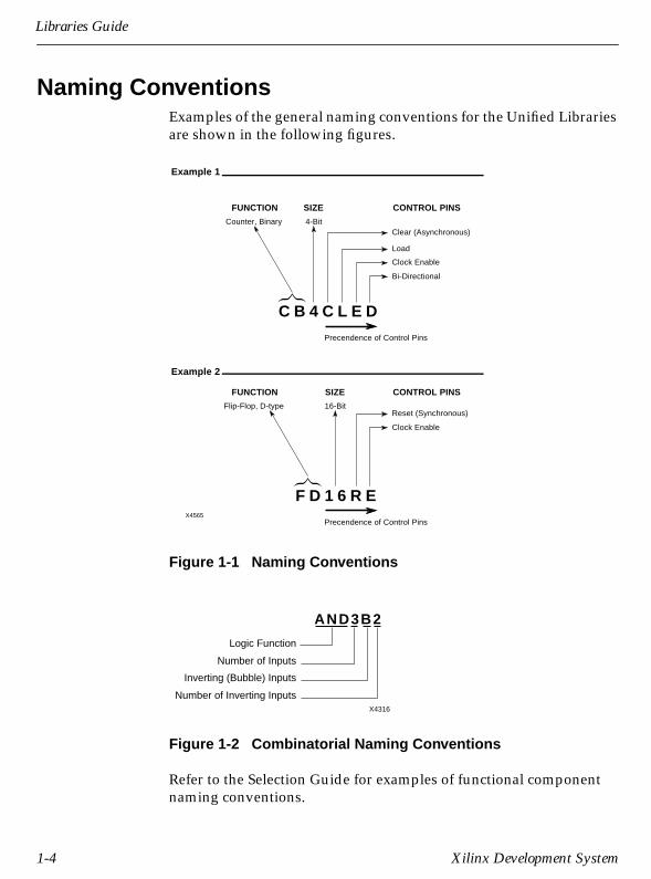
Naming ConventionsExamples of the general naming conventions for the Unified Librariesare shown in the following figures.
Figure 1-1 Naming Conventions
Figure 1-2 Combinatorial Naming Conventions
Refer to the Selection Guide for examples of functional componentnaming conventions.
X4565
Clear (Asynchronous)4-BitCounter, Binary
Precendence of Control Pins
Load
Clock Enable
Bi-Directional
C B 4 C L E D
CONTROL PINSSIZEFUNCTION
Example 1
Example 2
16-BitFlip-Flop, D-type
Precendence of Control Pins
Reset (Synchronous)
Clock Enable
F D 1 6 R E
CONTROL PINSSIZEFUNCTION
X4316
AND3B2
Logic Function
Number of Inputs
Inverting (Bubble) Inputs
Number of Inverting Inputs
1-4 Xilinx Development System

Xilinx Unified Libraries
Flip-Flop, Counter, and Register PerformanceAll counter, register, and storage functions are derived from the flip-flops (and latches in XC2000) available in the Configurable LogicBlocks (CLBs).
The D flip-flop is the basic building block for all four architectures.Differences occur from the availability of asynchronous Clear (CLR)and Preset (PRE) inputs, and the source of the synchronous controlsignals, such as, Clock Enable (CE), Clock (C), Load enable (L),synchronous Reset (R), and synchronous Set (S). The basic flip-flopconfiguration for each architecture follows.
The basic XC2000 and XC7000 flip-flops have both Clear and Presetinputs.
The XC3000 has a direct-connect Clock Enable input and a Clearinput.
The XC4000 has a direct-connect Clock Enable input and a choice ofeither the Clear or the Preset inputs, but not both.
Q
D
C
FDCP
PRE
CLR X4397
X3717CLR
C
CE
QDFDCE
X3717CLR
C
CE
QDFDCE
X3721
FDPE
C
CE
QD
PRE
Libraries Guide 1-5

Libraries Guide
The asynchronous and synchronous control functions, when used,have a priority that is consistent across all devices and architectures.These inputs can be either active-High or active-Low as defined bythe macro. The priority, from highest to lowest is as follows.
● Asynchronous Clear (C)
● Asynchronous Preset (PRE)
● Synchronous Set (S)
● Synchronous Reset (R)
● Load Enable (L)
● Shift Left/Right (LEFT)
● Clock Enable (CE)
Note: The asynchronous C and PRE inputs, by definition, have prior-ity over all the synchronous control and clock inputs.
The Clock Enable (CE) function is implemented using two differentmethods in the Xilinx Unified Libraries; both are shown in thefollowing figure. In method 1, CE is implemented by connecting theCE pin of the macro directly to the dedicated Enable Clock (EC) pin ofthe internal Configurable Logic Block (CLB) flip-flop. In method 2,CE is implemented using function generator logic. CE takes prece-dence over the L, S, and R inputs in method 1. CE has the samepriority as the L, S, and R inputs in method 2. The method used in aparticular macro is indicated in the macro’s description.
1-6 Xilinx Development System

Xilinx Unified Libraries
Figure 1-3 Clock Enable Implementation Methods
X4675
EC
Method 1 CE implemented
using dedicated EC pin.
Method 2 CE implemented as a
function generator input.
CE
C
EC
C
C
C
C1
C2
C1
C2
C1
CE
C2
C1
C2
CEQ
QFunction
Generator
FunctionGenerator
FunctionGenerator
FunctionGenerator
Libraries Guide 1-7

Libraries Guide
1-8 Xilinx Development System
Chapter 2
Libraries Guide — 0401410 01 2-1
Selection GuideThe Selection Guide briefly describes, then tabularly lists the macrologic elements that are described in detail in the “Design Elements”chapter. The tables included in this section are organized into func-tional categories specifying all the available macros from each of theXC2000, XC3000, XC4000, and XC7000 families. The tables categorizethe elements into sub-categories based on similar functions. Thesequence of each sub-category is based on an ascending order ofcomplexity. The categories are as follows.
● Arithmetic functions
● Buffers
● Comparators
● Counters
● Data registers
● Decoders
● Edge decoders
● Encoders
● Flip-Flops
● General
● Input/output flip-flops
● Input/output functions
● Input latches
● Latches
● Logic primitives
● Map elements
● Memory elements

Libraries Guide
● Multiplexers
● PLD elements
● Shift registers
● Shifters
The elements from each architecture that provide the same functionare listed adjacent to each other in the table, even though they mightnot have the same name. For particular elements, use the name speci-fied for the architecture of interest.
Note: When converting your design between FPGA families, usemacros that have equivalent functions in each of the families to mini-mize re-designing.
There are a number of standard TTL 7400-type functions in theXC2000, XC3000, XC4000, and XC7000 architectures. All 7400-typefunctions are in alphanumeric order starting with “X,” and thenumeric sequence uses ascending numbers following the “74” prefix.For example, X74_42 precedes X74_138.
Functional CategoriesThe following sections briefly describe, then tabularly list the UnifiedLibraries design element functions by category. Elements are listed inalphanumeric order according to architecture in each applicablearchitecture column. N/A means the element does not exist in thatparticular architecture.
Following these functional listings, replacement and obsoleteelements are discussed.
2-2 Xilinx Development System

Selection Guide
Arithmetic FunctionsThere are three types of arithmetic functions: accumulators (ACC),adders (ADD), and adder/subtracters (ADSU). With an ADSU, eitherunsigned binary or twos-complement operations cause an overflow.If the result crosses the overflow boundary, an overflow is generated.Similarly, when the result crosses the carry-out boundary, a carry-outis generated. The following figure shows the ADSU carry-out andoverflow boundaries.
Figure 2-1 ADSU Carry-Out and Overflow Boundaries
XC2000 XC3000 XC4000 XC7000 Description
ACC1 N/A N/A ACC1 1-Bit Accumulator with Carry-In,Carry-Out, and Synchronous Reset
N/A N/A N/A ACC1X1 1-Bit Accumulator with Carry-Out forEPLD
N/A N/A N/A ACC1X2 1-Bit Accumulator with Carry-In andCarry-Out for EPLD
N/A ACC4 ACC4 ACC4 4-Bit Accumulator with Carry-In,Carry-Out, and Synchronous Reset
N/A N/A N/A ACC4X1 4-Bit Accumulator with Carry-Out forEPLD
N/A N/A N/A ACC4X2 4-Bit Accumulator with Carry-In andCarry-Out for EPLD
N/A ACC8 ACC8 ACC8 8-Bit Accumulator with Carry-In,Carry-Out, and Synchronous Reset
TWO
SC
OM
PL
EM
EN
TO
RS
IGNED
TW
OSC
OM
PL
EM
EN
TO
RS
IGN
ED
UNS
IGN
ED
BIN
AR
Y
UN
SIG
NE
DB
INA
RY
X4720
255
-127 127
127128
0
0-1
Overflow
Carry-Out
Libraries Guide 2-3

Libraries Guide
N/A N/A N/A ACC8X1 8-Bit Accumulator with Carry-Out forEPLD
N/A N/A N/A ACC8X2 8-Bit Accumulator with Carry-In andCarry-Out for EPLD
N/A ACC16 ACC16 ACC16 16-Bit Accumulator with Carry-In,Carry-Out, and Synchronous Reset
N/A N/A N/A ACC16X1 16-Bit Accumulator with Carry-Out forEPLD
N/A N/A N/A ACC16X2 16-Bit Accumulator with Carry-In andCarry-Out for EPLD
ADD1 N/A N/A ADD1 1-Bit Full Adder with Carry-In andCarry-Out
N/A N/A N/A ADD1X1 1-Bit Adder with Carry-Out for EPLDN/A N/A N/A ADD1X2 1-Bit Adder with Carry-In and Carry-
Out for EPLDN/A ADD4 ADD4 ADD4 4-Bit Cascadable Full Adder with
Carry-In and Carry-OutN/A N/A N/A ADD4X1 4-Bit Adder with Carry-Out for EPLDN/A N/A N/A ADD4X2 4-Bit Adder with Carry-In and
Carry-Out for EPLDN/A ADD8 ADD8 ADD8 8-Bit Cascadable Full Adder with
Carry-In and Carry-OutN/A N/A N/A ADD8X1 8-Bit Adder with Carry-Out for EPLDN/A N/A N/A ADD8X2 8-Bit Adder with Carry-In and
Carry-Out for EPLDN/A ADD16 ADD16 ADD16 16-Bit Cascadable Full Adder with
Carry-In and Carry-OutN/A N/A N/A ADD16X1 16-Bit Adder with Carry-Out for EPLDN/A N/A N/A ADD16X2 16-Bit Adder with Carry-In and
Carry-Out for EPLDADSU1 N/A N/A ADSU1 1-Bit Adder/Substracter with Carry-In
and Carry-OutN/A N/A N/A ADSU1X1 1-Bit Adder/Subtracter with
Carry-Out for EPLDN/A N/A N/A ADSU1X2 1-Bit Adder/Subtracter with Carry-In
and Carry-Out for EPLDN/A ADSU4 ADSU4 ADSU4 4-Bit Cascadable Adder/Subtracter
with Carry-In and Carry-Out
XC2000 XC3000 XC4000 XC7000 Description
2-4 Xilinx Development System

Selection Guide
BuffersThe buffers in this section route high fan-out signals, 3-state signals,and clocks inside a PLD device. The “Input/Output Functions”section later in this chapter covers off-chip interface buffers.
N/A N/A N/A ADSU4X1 4-Bit Adder/Subtracter withCarry-Out for EPLD
N/A N/A N/A ADSU4X2 4-Bit Adder/Subtracter with Carry-Inand Carry-Out for EPLD
N/A ADSU8 ADSU8 ADSU8 8-Bit Adder/Subtracter with Carry-In,Carry-Out, and Overflow
N/A N/A N/A ADSU8X1 8-Bit Adder/Subtracter withCarry-Out for EPLD
N/A N/A N/A ADSU8X2 8-Bit Adder/Subtracter with Carry-Inand Carry-Out for EPLD
N/A ADSU16 ADSU16 ADSU16 16-Bit Adder/Subtracter withOverflow
N/A N/A N/A ADSU16X1 16-Bit Adder/Subtracter withCarry-Out for EPLD
N/A N/A N/A ADSU16X2 16-Bit Adder/Subtracter withCarry-In and Carry-Out for EPLD
X74_280 X74_280 X74_280 X74_280 9-Bit Odd/Even Parity Generator/Checker
X74_283 X74_283 X74_283 X74_283 4-Bit Full Adder with Carry-In andCarry-Out
XC2000 XC3000 XC4000 XC7000 Description
ACLK ACLK N/A N/A Alternate Clock BufferBUF BUF BUF BUF General Purpose BuffersN/A N/A N/A BUF4,
BUF8,BUF16
N/A N/A N/A BUFCE Global Clock-Enable Input Bufferfor EPLD
XC2000 XC3000 XC4000 XC7000 Description
Libraries Guide 2-5

Libraries Guide
ComparatorsThere are two types of comparators, identity (COMP) and magnitude(COMPM).
N/A BUFE,BUFE4,BUFE8,BUFE16
BUFE,BUFE4,BUFE8,BUFE16
BUFE,BUFE4,BUFE8,BUFE16
Internal 3-State Buffers withActive-High Enable
N/A N/A N/A BUFFOE Global Fast-Output-Enable (FOE)Input Buffer for EPLD
BUFG BUFG BUFG BUFG Global Clock BufferN/A N/A BUFGP BUFGP Primary Global Buffer for Driving
Clocks or Longlines (4 per device)N/A N/A BUFGS BUFGS Secondary Global Buffer for Driv-
ing Clocks or LonglinesN/A N/A BUFOD N/A Open-Drain BufferN/A BUFT,
BUFT4,BUFT8,BUFT16
BUFT,BUFT4,BUFT8,BUFT16
BUFT,BUFT4,BUFT8,BUFT16
Internal 3-State Buffers withActive-Low Enable
GCLK GCLK N/A N/A Global Clock Buffer
XC2000 XC3000 XC4000 XC7000 Description
COMP2 COMP2 COMP2 COMP2 2-Bit Identity ComparatorCOMP4 COMP4 COMP4 COMP4 4-Bit Identity ComparatorCOMP8 COMP8 COMP8 COMP8 8-Bit Identity ComparatorCOMP16 COMP16 COMP16 COMP16 16-Bit Identity ComparatorCOMPM2 COMPM2 COMPM2 COMPM2 2-Bit Magnitude ComparatorCOMPM4 COMPM4 COMPM4 COMPM4 4-Bit Magnitude ComparatorCOMPM8 COMPM8 COMPM8 COMPM8 8-Bit Magnitude ComparatorCOMPM16 COMPM16 COMPM16 N/A 16-Bit Magnitude ComparatorN/A N/A COMPMC8 N/A 8-Bit Magnitude ComparatorN/A N/A COMPMC16 N/A 16-Bit Magnitude ComparatorX74_L85 X74_L85 X74_L85 X74_L85 4-Bit Expandable Magnitude
Comparator
XC2000 XC3000 XC4000 XC7000 Description
2-6 Xilinx Development System

Selection Guide
CountersThere are six types of counters with various synchronous and asyn-chronous inputs. The name of the counter defines the modulo or bitsize, the counter type, and which control functions are included. Thecounter naming convention is shown in the following figure.
Figure 2-2 Counter Naming Convention
A carry-lookahead design accommodates large counters withoutextra gating. On TTL 7400-type counters with trickle clock enable(ENT), parallel clock enable (ENP), and ripple carry-out (RCO), boththe ENT and ENP inputs must be High to count. ENT is propagatedforward to enable RCO, which produces a High output with theapproximate duration of the QA output. The following figure illus-trates a carry-lookahead design.
X74_518 X74_518 X74_518 X74_518 8-Bit Identity Comparator withActive-Low Enable
X74_521 X74_521 X74_521 X74_521 8-Bit Identity Comparator withActive-Low Enable and Output
XC2000 XC3000 XC4000 XC7000 Description
X4577
Binary (B)BCD (D)Binary, Carry Logic (C)Johnson (J)Ripple (R)
Counter
Asynchronous Clear (C)Synchronous Reset (R)
Modulo (Bit Size)
Loadable
C B 1 6 C L E D
Clock Enable
Directional
Libraries Guide 2-7

Libraries Guide
Figure 2-3 Carry-Lookahead Design
The RCO output of the first stage of the ripple carry is connected tothe ENP input of the second stage and all subsequent stages. TheRCO output of second stage and all subsequent stages is connected tothe ENT input of the next stage. The ENT of the second stage isalways enabled/tied to VCC. CE is always connected to the ENTinput of the first stage. This cascading method allows the first stage ofthe ripple carry to be built as a prescaler. In other words, the firststage is built to count very fast.
X4719
ENT
ENP
RCO
ENT
ENP
RCO
ENT
ENP
RCOVcc
Vcc
ENTCE
ENP
RCO
2-8 Xilinx Development System

Selection Guide
XC2000 XC3000 XC4000 XC7000 Description
CB2CE CB2CE CB2CE CB2CE 2-Bit Cascadable Binary Counterwith Clock Enable and Asynchro-nous Clear
CB2CLE CB2CLE CB2CLE CB2CLE 2-Bit Loadable Cascadable BinaryCounter with Clock Enable andAsynchronous Clear
CB2CLED CB2CLED CB2CLED CB2CLED 2-Bit Loadable Cascadable Bidi-rectional Binary Counter withClock Enable and AsynchronousClear
CB2RE CB2RE CB2RE CB2RE 2-Bit Cascadable Binary Counterwith Clock Enable and Synchro-nous Reset
N/A N/A N/A CB2RLE 2-Bit Loadable Cascadable BinaryCounter with Clock Enable andSynchronous Reset
N/A N/A N/A CB2X1 2-Bit Loadable Cascadable Bidi-rectional Binary Counter withAsynchronous Clear for EPLD
N/A N/A N/A CB2X2 2-Bit Loadable Cascadable Bidi-rectional Binary Counter withSynchronous Reset for EPLD
CB4CE CB4CE CB4CE CB4CE 4-Bit Cascadable Binary Counterwith Clock Enable and Asynchro-nous Clear
CB4CLE CB4CLE CB4CLE CB4CLE 4-Bit Loadable Cascadable BinaryCounter with Clock Enable andAsynchronous Clear
CB4CLED CB4CLED CB4CLED CB4CLED 4-Bit Loadable Cascadable Bidi-rectional Binary Counter withClock Enable and AsynchronousClear
CB4RE CB4RE CB4RE CB4RE 4-Bit Cascadable Binary Counterwith Clock Enable and Synchro-nous Reset
Libraries Guide 2-9

Libraries Guide
N/A N/A N/A CB4RLE 4-Bit Loadable Cascadable BinaryCounter with Clock Enable andSynchronous Reset
N/A N/A N/A CB4X1 4-Bit Loadable Cascadable Bidi-rectional Binary Counter withAsynchronous Clear for EPLD
N/A N/A N/A CB4X2 4-Bit Loadable Cascadable Bidi-rectional Binary Counter withSynchronous Reset for EPLD
CB8CE CB8CE CB8CE CB8CE 8-Bit Cascadable Binary Counterwith Clock Enable and Asynchro-nous Clear
CB8CLE CB8CLE CB8CLE CB8CLE 8-Bit Loadable Cascadable BinaryCounter with Clock Enable andAsynchronous Clear
CB8CLED CB8CLED CB8CLED CB8CLED 8-Bit Loadable Cascadable Bidi-rectional Binary Counter withClock Enable and AsynchronousClear
CB8RE CB8RE CB8RE CB8RE 8-Bit Cascadable Binary Counterwith Clock Enable and Synchro-nous Reset
N/A N/A N/A CB8RLE 8-Bit Loadable Cascadable BinaryCounter with Clock Enable andSynchronous Reset
N/A N/A N/A CB8X1 8-Bit Loadable Cascadable Bidi-rectional Binary Counter withAsynchronous Clear for EPLD
N/A N/A N/A CB8X2 8-Bit Loadable Cascadable Bidi-rectional Binary Counter withSynchronous Reset for EPLD
CB16CE CB16CE CB16CE CB16CE 16-Bit Cascadable Binary Counterwith Clock Enable and Asynchro-nous Clear
CB16CLE CB16CLE CB16CLE CB16CLE 16-Bit Loadable CascadableBinary Counter with ClockEnable and Asynchronous Clear
XC2000 XC3000 XC4000 XC7000 Description
2-10 Xilinx Development System
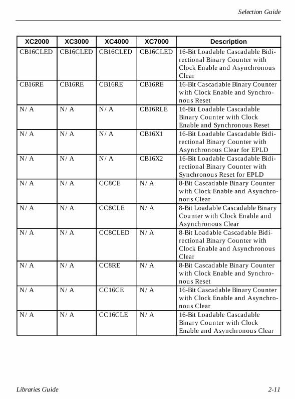
Selection Guide
CB16CLED CB16CLED CB16CLED CB16CLED 16-Bit Loadable Cascadable Bidi-rectional Binary Counter withClock Enable and AsynchronousClear
CB16RE CB16RE CB16RE CB16RE 16-Bit Cascadable Binary Counterwith Clock Enable and Synchro-nous Reset
N/A N/A N/A CB16RLE 16-Bit Loadable CascadableBinary Counter with ClockEnable and Synchronous Reset
N/A N/A N/A CB16X1 16-Bit Loadable Cascadable Bidi-rectional Binary Counter withAsynchronous Clear for EPLD
N/A N/A N/A CB16X2 16-Bit Loadable Cascadable Bidi-rectional Binary Counter withSynchronous Reset for EPLD
N/A N/A CC8CE N/A 8-Bit Cascadable Binary Counterwith Clock Enable and Asynchro-nous Clear
N/A N/A CC8CLE N/A 8-Bit Loadable Cascadable BinaryCounter with Clock Enable andAsynchronous Clear
N/A N/A CC8CLED N/A 8-Bit Loadable Cascadable Bidi-rectional Binary Counter withClock Enable and AsynchronousClear
N/A N/A CC8RE N/A 8-Bit Cascadable Binary Counterwith Clock Enable and Synchro-nous Reset
N/A N/A CC16CE N/A 16-Bit Cascadable Binary Counterwith Clock Enable and Asynchro-nous Clear
N/A N/A CC16CLE N/A 16-Bit Loadable CascadableBinary Counter with ClockEnable and Asynchronous Clear
XC2000 XC3000 XC4000 XC7000 Description
Libraries Guide 2-11

Libraries Guide
N/A N/A CC16CLED N/A 16-Bit Loadable Cascadable Bidi-rectional Binary Counter withClock Enable and AsynchronousClear
N/A N/A CC16RE N/A 16-Bit Cascadable Binary Counterwith Clock Enable and Synchro-nous Reset
CD4CE CD4CE CD4CE CD4CE 4-Bit Cascadable BCD Counterwith Clock Enable and Asynchro-nous Clear
CD4CLE CD4CLE CD4CLE CD4CLE 4-Bit Loadable Cascadable BCDCounter with Clock Enable andAsynchronous Clear
CD4RE CD4RE CD4RE CD4RE 4-Bit Cascadable BCD Counterwith Clock Enable and Synchro-nous Reset
CD4RLE CD4RLE CD4RLE CD4RLE 4-Bit Loadable Cascadable BCDCounter with Clock Enable andSynchronous Reset
CJ4CE CJ4CE CJ4CE CJ4CE 4-Bit Johnson Counter with ClockEnable and Asynchronous Clear
CJ4RE CJ4RE CJ4RE CJ4RE 4-Bit Johnson Counter with ClockEnable and Synchronous Reset
CJ5CE CJ5CE CJ5CE CJ5CE 5-Bit Johnson Counter with ClockEnable and Asynchronous Clear
CJ5RE CJ5RE CJ5RE CJ5RE 5-Bit Johnson Counter with ClockEnable and Synchronous Reset
CJ8CE CJ8CE CJ8CE CJ8CE 8-Bit Johnson Counter with ClockEnable and Asynchronous Clear
CJ8RE CJ8RE CJ8RE CJ8RE 8-Bit Johnson Counter with ClockEnable and Synchronous Reset
CR8CE CR8CE CR8CE CR8CE 8-Bit Negative-Edge Binary Rip-ple Counter with Clock Enableand Asynchronous Clear
CR16CE CR16CE CR16CE CR16CE 16-Bit Negative-Edge Binary Rip-ple Counter with Clock Enableand Asynchronous Clear
XC2000 XC3000 XC4000 XC7000 Description
2-12 Xilinx Development System

Selection Guide
X74_160 X74_160 X74_160 X74_160 4-Bit Loadable Cascadable BCDCounter with Parallel and TrickleEnables and Asynchronous Clear
X74_161 X74_161 X74_161 X74_161 4-Bit Loadable Cascadable BinaryCounter with Parallel and TrickleEnables and Asynchronous Clear
X74_162 X74_162 X74_162 X74_162 4-Bit Loadable Cascadable BCDCounter with Parallel and TrickleEnables and Synchronous Reset
X74_163 X74_163 X74_163 X74_163 4-Bit Loadable Cascadable BinaryCounter with Parallel and TrickleEnables and Synchronous Reset
X74_168 X74_168 X74_168 X74_168 4-Bit Loadable Cascadable Bidi-rectional BCD Counter with Par-allel and Trickle Enables
X74_390 X74_390 X74_390 X74_390 4-Bit BCD/Bi-Quinary RippleCounter with Negative-EdgeClocks and Asynchronous Clear
XC2000 XC3000 XC4000 XC7000 Description
Libraries Guide 2-13

Libraries Guide
Data RegistersThere are three TTL 7400-type data registers designed to functionexactly as the TTL elements for which they are named.
DecodersDecoder names, shown in the following figure, indicate the numberof inputs and outputs and if an enable is available. Decoders with anenable can be used as multiplexers. This group includes some stan-dard TTL 7400-type decoders whose names have an “X74” prefix.
Figure 2-4 Decoder Naming Convention
XC2000 XC3000 XC4000 XC7000 Description
X74_174 X74_174 X74_174 X74_174 6-Bit Data Register with Active-Low Asynchronous Clear
X74_273 X74_273 X74_273 X74_273 8-Bit Data Register with Active-Low Asynchronous Clear
X74_377 X74_377 X74_377 X74_377 8-Bit Data Register with Active-Low Clock Enable
XC2000 XC3000 XC4000 XC7000 Description
D2_4E D2_4E D2_4E D2_4E 2- to 4-Line Decoder/Demulti-plexer with Enable
D3_8E D3_8E D3_8E D3_8E 3- to 8-Line Decoder/Demulti-plexer with Enable
D4_16E D4_16E D4_16E D4_16E 4- to 16-Line Decoder/Demulti-plexer with Enable
X74_42 X74_42 X74_42 X74_42 4- to 10-Line BCD-to-DecimalDecoder with Active-Low Outputs
X4619
D 2 _ 4 EDecoder
Number of Inputs
Number of Outputs
Output Enable
2-14 Xilinx Development System

Selection Guide
Edge DecodersEdge decoders are open-drain wired-AND gates that are available indifferent bit sizes.
EncodersThere are two priority encoders (ENCPR) that function like the TTL7400-type elements they are named after. There is a 10- to 4-line BCDencoder and an 8- to 3-line binary encoder.
X74_138 X74_138 X74_138 X74_138 3- to 8-Line Decoder/Demulti-plexer with Active-Low Outputsand Three Enables
X74_139 X74_139 X74_139 X74_139 2- to 4-Line Decoder/Demulti-plexer with Active-Low Outputsand Active-Low Enable
X74_154 X74_154 X74_154 X74_154 4- to 16-Line Decoder/Demulti-plexer with Two Enables andActive-Low Outputs
XC2000 XC3000 XC4000 XC7000 Description
N/A N/A DECODE4 N/A 4-Bit Active-Low DecoderN/A N/A DECODE8 N/A 8-Bit Active-Low DecoderN/A N/A DECODE16 N/A 16-Bit Active-Low Decoder
XC2000 XC3000 XC4000 XC7000 Description
X74_147 X74_147 X74_147 X74_147 10- to 4-Line Priority Encoder withActive-Low Inputs and Outputs
X74_148 X74_148 X74_148 X74_148 8- to 3-Line Cascadable PriorityEncoder with Active-Low Inputsand Outputs
XC2000 XC3000 XC4000 XC7000 Description
Libraries Guide 2-15
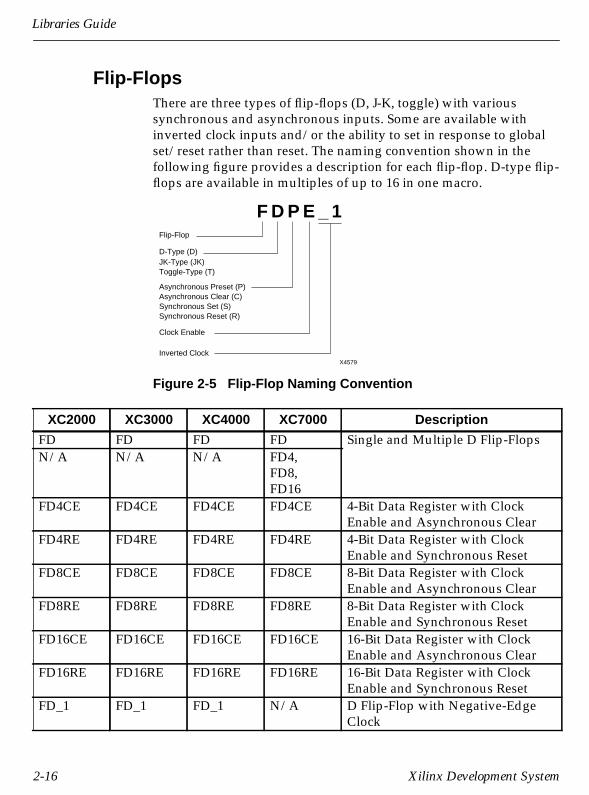
Libraries Guide
Flip-FlopsThere are three types of flip-flops (D, J-K, toggle) with varioussynchronous and asynchronous inputs. Some are available withinverted clock inputs and/or the ability to set in response to globalset/reset rather than reset. The naming convention shown in thefollowing figure provides a description for each flip-flop. D-type flip-flops are available in multiples of up to 16 in one macro.
Figure 2-5 Flip-Flop Naming Convention
XC2000 XC3000 XC4000 XC7000 Description
FD FD FD FD Single and Multiple D Flip-FlopsN/A N/A N/A FD4,
FD8,FD16
FD4CE FD4CE FD4CE FD4CE 4-Bit Data Register with ClockEnable and Asynchronous Clear
FD4RE FD4RE FD4RE FD4RE 4-Bit Data Register with ClockEnable and Synchronous Reset
FD8CE FD8CE FD8CE FD8CE 8-Bit Data Register with ClockEnable and Asynchronous Clear
FD8RE FD8RE FD8RE FD8RE 8-Bit Data Register with ClockEnable and Synchronous Reset
FD16CE FD16CE FD16CE FD16CE 16-Bit Data Register with ClockEnable and Asynchronous Clear
FD16RE FD16RE FD16RE FD16RE 16-Bit Data Register with ClockEnable and Synchronous Reset
FD_1 FD_1 FD_1 N/A D Flip-Flop with Negative-EdgeClock
X4579
D-Type (D)
Flip-Flop
JK-Type (JK)Toggle-Type (T)
Asynchronous Preset (P)Asynchronous Clear (C)Synchronous Set (S)Synchronous Reset (R)
Inverted Clock
Clock Enable
F D P E _ 1
2-16 Xilinx Development System

Selection Guide
FDC FDC FDC FDC D Flip-Flop with AsynchronousClear
FDC_1 FDC_1 FDC_1 N/A D Flip-Flop with Negative-EdgeClock and Asynchronous Clear
FDCE FDCE FDCE FDCE D Flip-Flop with Clock Enable andAsynchronous Clear
FDCE_1 FDCE_1 FDCE_1 N/A D Flip-Flop with Negative-EdgeClock, Clock Enable, and Asyn-chronous Clear
FDCP N/A N/A FDCP D Flip-Flop with AsynchronousPreset and Clear
FDCPE N/A N/A FDCPE D Flip-Flop with Clock Enable andAsynchronous Preset and Clear
N/A N/A FDP FDP D Flip-Flop with AsynchronousPreset
N/A N/A FDP_1 N/A D Flip-Flop with Negative-EdgeClock and Asynchronous Preset
N/A N/A FDPE FDPE D Flip-Flop with Clock Enable andAsynchronous Preset
N/A N/A FDPE_1 N/A D Flip-Flop with Negative-EdgeClock, Clock Enable, and Asyn-chronous Preset
FDR FDR FDR FDR D Flip-Flop with SynchronousReset
FDRE FDRE FDRE FDRE D Flip-Flop with Clock Enable andSynchronous Reset
FDRS FDRS FDRS FDRS D Flip-Flop with SynchronousReset and Synchronous Set
FDRSE FDRSE FDRSE FDRSE D Flip-Flop with SynchronousReset and Set and Clock Enable
FDS FDS FDS FDS D Flip-Flop with Synchronous SetFDSE FDSE FDSE FDSE D Flip-Flop with Clock Enable and
Synchronous SetFDSR FDSR FDSR FDSR D Flip-Flop with Synchronous Set
and ResetFDSRE FDSRE FDSRE FDSRE D Flip-Flop with Synchronous Set
and Reset and Clock Enable
XC2000 XC3000 XC4000 XC7000 Description
Libraries Guide 2-17

Libraries Guide
FJKC FJKC FJKC FJKC J-K Flip-Flop with AsynchronousClear
FJKCE FJKCE FJKCE FJKCE J-K Flip-Flop with Clock Enableand Asynchronous Clear
FJKCP N/A N/A FJKCP J-K Flip-Flop with AsynchronousClear and Preset
FJKCPE N/A N/A FJKCPE J-K Flip-Flop with AsynchronousClear and Preset and Clock Enable
N/A N/A FJKP FJKP J-K Flip-Flop with AsynchronousPreset
N/A N/A FJKPE FJKPE J-K Flip-Flop with Clock Enableand Asynchronous Preset
FJKRSE FJKRSE FJKRSE FJKRSE J-K Flip-Flop with Clock Enableand Synchronous Reset and Set
FJKSRE FJKSRE FJKSRE FJKSRE J-K Flip-Flop with Clock Enableand Synchronous Set and Reset
FTC FTC FTC FTC Toggle Flip-Flop with ToggleEnable and Asynchronous Clear
FTCE FTCE FTCE FTCE Toggle Flip-Flop with Toggle andClock Enable and AsynchronousClear
FTCLE FTCLE FTCLE FTCLE Toggle/Loadable Flip-Flop withToggle and Clock Enable and Asyn-chronous Clear
FTCP N/A N/A FTCP Toggle Flip-Flop with ToggleEnable and Asynchronous Clearand Preset
FTCPE N/A N/A FTCPE Toggle Flip-Flop with Toggle andClock Enable and AsynchronousClear and Preset
FTCPLE N/A N/A FTCPLE Loadable Toggle Flip-Flop withToggle and Clock Enable and Asyn-chronous Clear and Preset
N/A N/A FTP FTP Toggle Flip-Flop with ToggleEnable and Asynchronous Preset
N/A N/A FTPE FTPE Toggle Flip-Flop with Toggle andClock Enable and AsynchronousPreset
XC2000 XC3000 XC4000 XC7000 Description
2-18 Xilinx Development System
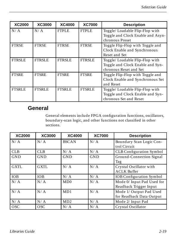
Selection Guide
GeneralGeneral elements include FPGA configuration functions, oscillators,boundary-scan logic, and other functions not classified in othersections.
N/A N/A FTPLE FTPLE Toggle/Loadable Flip-Flop withToggle and Clock Enable and Asyn-chronous Preset
FTRSE FTRSE FTRSE FTRSE Toggle Flip-Flop with Toggle andClock Enable and SynchronousReset and Set
FTRSLE FTRSLE FTRSLE FTRSLE Toggle/Loadable Flip-Flop withToggle and Clock Enable and Syn-chronous Reset and Set
FTSRE FTSRE FTSRE FTSRE Toggle Flip-Flop with Toggle andClock Enable and Synchronous Setand Reset
FTSRLE FTSRLE FTSRLE FTSRLE Toggle/Loadable Flip-Flop withToggle and Clock Enable and Syn-chronous Set and Reset
XC2000 XC3000 XC4000 XC7000 Description
N/A N/A BSCAN N/A Boundary Scan Logic Con-trol Circuit
CLB CLB N/A N/A CLB Configuration SymbolGND GND GND GND Ground-Connection Signal
TagGXTL GXTL N/A N/A Crystal Oscillator with
ACLK BufferIOB IOB N/A N/A IOB Configuration SymbolN/A N/A MD0 N/A Mode 0/Input Pad Used for
Readback Trigger InputN/A N/A MD1 N/A Mode 1/Output Pad Used
for Readback Data OutputN/A N/A MD2 N/A Mode 2/Input PadOSC OSC N/A N/A Crystal Oscillator
XC2000 XC3000 XC4000 XC7000 Description
Libraries Guide 2-19

Libraries Guide
N/A N/A OSC4 N/A Internal 5-Frequency Clock-Signal Generator
N/A N/A PULLDOWN N/A Resistor to GND for InputPads
N/A PULLUP PULLUP PULLUP Resistor to VCC for InputPADs, Open-Drain and3-State Outputs
N/A N/A READBACK N/A FPGA Bitstream ReadbackController
N/A N/A STARTUP N/A User Interface to GlobalClock, Reset, and 3-StateControls
N/A N/A TCK N/A Boundary-Scan Test ClockInput Pad
N/A N/A TDI N/A Boundary-Scan Test DataInput Pad
N/A N/A TDO N/A Boundary-Scan Data Out-put Pad
N/A TIMEGRP TIMEGRP N/A Schematic-Level Table ofBasic Timing SpecificationGroups
N/A TIMESPEC TIMESPEC TIMESPEC Schematic-Level TimingRequirement Table
N/A N/A TMS N/A Boundary-Scan Test ModeSelect Input Pad
XC2000 XC3000 XC4000 XC7000 Description
2-20 Xilinx Development System

Selection Guide
Input/Output Flip-FlopsInput/output flip-flops are configured in IOBs. They include flip-flops whose outputs are enabled by 3-state buffers, flip-flops that canbe set upon global set/reset rather than reset, and flip-flops withinverted clock inputs. The naming convention specifies each flip-flopfunction and is illustrated in the following figure.
Figure 2-6 Input/Output Flip-Flop Naming Convention
XC2000 XC3000 XC4000 XC7000 Description
IFD,IFD4,IFD8,IFD16
IFD,IFD4,IFD8,IFD16
IFD,IFD4,IFD8,IFD16
IFD,IFD4,IFD8,IFD16
Single- and Multiple-InputD Flip-Flops
IFD_1 IFD_1 IFD_1 N/A D Flip-Flop with Inverted ClockN/A N/A N/A IFDX1,
IFD4X1,IFD8X1,IFD16X1
Input D Flip-Flops with ClockEnable for EPLD
N/A N/A IFDI N/A Input D Flip-Flop (AsynchronousSet)
N/A N/A IFDI_1 N/A D Flip-Flop with Inverted Clock(Asynchronous Set)
N/A OFD,OFD4,OFD8,OFD16
OFD,OFD4,OFD8,OFD16
OFD,OFD4,OFD8,OFD16
Single- and Multiple-OutputD Flip-Flops
N/A OFD_1 OFD_1 N/A Output D Flip-Flop with InvertedClock
X4580
Output (O), Input (I)
Flip-Flop
D-Type
Active High Enable (E)Active Low Enable (T)
Inverse of Normal Initial State
Inverted Clock
O F D E I _ 1
Libraries Guide 2-21

Libraries Guide
N/A OFDE,OFDE4,OFDE8,OFDE16
OFDE,OFDE4,OFDE8,OFDE16
OFDE,OFDE4,OFDE8,OFDE16
D Flip-Flops with Active-High3-State Output Buffers
N/A OFDE_1 OFDE_1 N/A D Flip-Flop with Active-High3-State Output Buffer and InvertedClock
N/A N/A OFDEI N/A D Flip-Flop with Active-High3-State Output Buffer (Asynchro-nous Set)
N/A N/A OFDEI_1 N/A D Flip-Flop with Active-High3-State Output Buffer and InvertedClock (Asynchronous Set)
N/A N/A OFDI N/A Output D Flip-Flop (AsynchronousSet)
N/A N/A OFDI_1 N/A Output D Flip-Flop with InvertedClock (Asynchronous Set)
N/A OFDT,OFDT4,OFDT8,OFDT16
OFDT,OFDT4,OFDT8,OFDT16
OFDT,OFDT4,OFDT8,OFDT16
Single and Multiple D Flip-Flopswith Active-Low 3-State OutputBuffers
N/A OFDT_1 OFDT_1 N/A D Flip-Flop with Active-Low3-State Output Buffer and InvertedClock
N/A N/A OFDTI N/A D Flip-Flop with Active-Low3-State Output Buffer (Asynchro-nous Set)
N/A N/A OFDTI_1 N/A D Flip-Flop with Active-Low3-State Output Buffer and InvertedClock (Asynchronous Set)
XC2000 XC3000 XC4000 XC7000 Description
2-22 Xilinx Development System

Selection Guide
Input/Output FunctionsInput/Output Block (IOB) resources are configured into variousI/O primitives and macros for convenience, such as, output buffers(OBUFs) and output buffers with an enable (OBUFEs). Pads used toconnect the circuit to PLD device pins are also included.
XC2000 XC3000 XC4000 XC7000 Description
IBUF,IBUF4,IBUF8,IBUF16
IBUF,IBUF4,IBUF8,IBUF16
IBUF,IBUF4,IBUF8,IBUF16
IBUF,IBUF4,IBUF8,IBUF16
Single- and Multiple-InputBuffers
IOPAD,IOPAD4,IOPAD8,IOPAD16
IOPAD,IOPAD4,IOPAD8,IOPAD16
IOPAD,IOPAD4,IOPAD8,IOPAD16
IOPAD,IOPAD4,IOPAD8,IOPAD16
Single- and Multiple-Input/Output Pads
IPAD,IPAD4,IPAD8,IPAD16
IPAD,IPAD4,IPAD8,IPAD16
IPAD,IPAD4,IPAD8,IPAD16
IPAD,IPAD4,IPAD8,IPAD16
Single- and Multiple-Input Pads
OBUF,OBUF4,OBUF8,OBUF16
OBUF,OBUF4,OBUF8,OBUF16
OBUF,OBUF4,OBUF8,OBUF16
OBUF,OBUF4,OBUF8,OBUF16
Single- and Multiple-OutputBuffers
OBUFE,OBUFE4,OBUFE8,OBUFE16
OBUFE,OBUFE4,OBUFE8,OBUFE16
OBUFE,OBUFE4,OBUFE8,OBUFE16
OBUFE,OBUFE4,OBUFE8,OBUFE16
3-State Output Buffers withActive-High Fast Output Enable
N/A N/A N/A OBUFEX1,OBUFE4X1,OBUFE8X1,OBUFEX2
3-State Output Buffers withActive-High Fast Output Enablefor EPLD
OBUFT,OBUFT4,OBUFT8,OBUFT16
OBUFT,OBUFT4,OBUFT8,OBUFT16
OBUFT,OBUFT4,OBUFT8,OBUFT16
OBUFT,OBUFT4,OBUFT8,OBUFT16
Single and Multiple 3-StateOutput Buffers with Active-LowEnable
OPAD,OPAD4,OPAD8,OPAD16
OPAD,OPAD4,OPAD8,OPAD16
OPAD,OPAD4,OPAD8,OPAD16
OPAD,OPAD4,OPAD8,OPAD16
Single- and Multiple-Output Pads
Libraries Guide 2-23

Libraries Guide
Input LatchesSingle and multiple input latches can hold transient data entering achip. Input latches use the same naming convention as I/O flip-flops.
LatchesLatches (LD) are only available in the XC2000 and XC7000 architec-tures. XC3000 and XC4000 latches that existed in previous macrolibraries are not recommended for new designs.
UPAD UPAD UPAD UPAD Connects the I/O Node of an IOBto the Internal PLD Circuit
VCC VCC VCC VCC VCC Connection Signal Tag
XC2000 XC3000 XC4000 XC7000 Description
N/A ILD,ILD4,ILD8,ILD16
ILD,ILD4,ILD8,ILD16
ILD,ILD4,ILD8,ILD16
Input Transparent Data Latches
N/A ILD_1 ILD_1 N/A Transparent Input Data Latch withInverted Gate
N/A N/A ILDI N/A Input Transparent Data Latch(Asynchronous Set)
N/A N/A ILDI_1 N/A Transparent Input Data Latch withInverted Gate (Synchronous Set)
XC2000 XC3000 XC4000 XC7000 Description
LD N/A N/A LD Single and Multiple TransparentData LatchesN/A N/A N/A LD4,
LD8,LD16
LD_1 N/A N/A N/A Transparent Data Latch withInverted Gate
LDC N/A N/A N/A Transparent Data Latch with Asyn-chronous Clear
LD4CE,LD8CE,LD16CE
N/A N/A N/A Transparent Data Latches withAsynchronous Clear and ClockEnable
XC2000 XC3000 XC4000 XC7000 Description
2-24 Xilinx Development System

Selection Guide
Logic PrimitivesCombinatorial logic gates that implement the basic Boolean functionsare available in XC2000, XC3000, XC4000, and XC7000 architectureswith up to five inputs in all combinations of inverted and non-inverted inputs, and with six to nine inputs non-inverted.
LDCP N/A N/A N/A Transparent Data Latch with Asyn-chronous Clear and Preset
LDCPE N/A N/A N/A Transparent Data Latch with Asyn-chronous Clear and Preset andClock Enable
LDC_1 N/A N/A N/A Transparent Data Latch with Asyn-chronous Clear and Inverted GateInput
XC2000 XC3000 XC4000 XC7000 Description
AND2,AND2B1,AND2B2,AND3,AND3B1,AND3B2,AND3B3,AND4,AND4B1,AND4B2,AND4B3,AND4B4,AND5,AND5B1,AND5B2,AND5B3,AND5B4,AND5B5,AND6,AND7,AND8,AND9
AND2,AND2B1,AND2B2,AND3,AND3B1,AND3B2,AND3B3,AND4,AND4B1,AND4B2,AND4B3,AND4B4,AND5,AND5B1,AND5B2,AND5B3,AND5B4,AND5B5,AND6,AND7,AND8,AND9
AND2,AND2B1,AND2B2,AND3,AND3B1,AND3B2,AND3B3,AND4,AND4B1,AND4B2,AND4B3,AND4B4,AND5,AND5B1,AND5B2,AND5B3,AND5B4,AND5B5,AND6,AND7,AND8,AND9
AND2,AND2B1,AND2B2,AND3,AND3B1,AND3B2,AND3B3,AND4,AND4B1,AND4B2,AND4B3,AND4B4,AND5,AND5B1,AND5B2,AND5B3,AND5B4,AND5B5,AND6,AND7,AND8,AND9
2- to 9-Input AND Gateswith Inverted andNon-Inverted Inputs
XC2000 XC3000 XC4000 XC7000 Description
Libraries Guide 2-25

Libraries Guide
INV,INV4,INV8,INV16
INV,INV4,INV8,INV16
INV,INV4,INV8,INV16
INV,INV4,INV8,INV16
Single and MultipleInverters
NAND2,NAND2B1,NAND2B2,NAND3,NAND3B1,NAND3B2,NAND3B3,NAND4,NAND4B1,NAND4B2,NAND4B3,NAND4B4,NAND5,NAND5B1,NAND5B2,NAND5B3,NAND5B4,NAND5B5,NAND6,NAND7,NAND8,NAND9
NAND2,NAND2B1,NAND2B2,NAND3,NAND3B1,NAND3B2,NAND3B3,NAND4,NAND4B1,NAND4B2,NAND4B3,NAND4B4,NAND5,NAND5B1,NAND5B2,NAND5B3,NAND5B4,NAND5B5,NAND6,NAND7,NAND8,NAND9
NAND2,NAND2B1,NAND2B2,NAND3,NAND3B1,NAND3B2,NAND3B3,NAND4,NAND4B1,NAND4B2,NAND4B3,NAND4B4,NAND5,NAND5B1,NAND5B2,NAND5B3,NAND5B4,NAND5B5,NAND6,NAND7,NAND8,NAND9
NAND2,NAND2B1,NAND2B2,NAND3,NAND3B1,NAND3B2,NAND3B3,NAND4,NAND4B1,NAND4B2,NAND4B3,NAND4B4,NAND5,NAND5B1,NAND5B2,NAND5B3,NAND5B4,NAND5B5,NAND6,NAND7,NAND8,NAND9
2- to 9-Input NANDGates with Inverted andNon-Inverted Inputs
XC2000 XC3000 XC4000 XC7000 Description
2-26 Xilinx Development System

Selection Guide
NOR2,NOR2B1,NOR2B2,NOR3,NOR3B1,NOR3B2,NOR3B3,NOR4,NOR4B1,NOR4B2,NOR4B3,NOR4B4,NOR5,NOR5B1,NOR5B2,NOR5B3,NOR5B4,NOR5B5,NOR6,NOR7,NOR8,NOR9
NOR2,NOR2B1,NOR2B2,NOR3,NOR3B1,NOR3B2,NOR3B3,NOR4,NOR4B1,NOR4B2,NOR4B3,NOR4B4,NOR5,NOR5B1,NOR5B2,NOR5B3,NOR5B4,NOR5B5,NOR6,NOR7,NOR8,NOR9
NOR2,NOR2B1,NOR2B2,NOR3,NOR3B1,NOR3B2,NOR3B3,NOR4,NOR4B1,NOR4B2,NOR4B3,NOR4B4,NOR5,NOR5B1,NOR5B2,NOR5B3,NOR5B4,NOR5B5,NOR6,NOR7,NOR8,NOR9
NOR2,NOR2B1,NOR2B2,NOR3,NOR3B1,NOR3B2,NOR3B3,NOR4,NOR4B1,NOR4B2,NOR4B3,NOR4B4,NOR5,NOR5B1,NOR5B2,NOR5B3,NOR5B4,NOR5B5,NOR6,NOR7,NOR8,NOR9
2- to 9-Input NOR Gateswith Inverted andNon-Inverted Inputs
XC2000 XC3000 XC4000 XC7000 Description
Libraries Guide 2-27

Libraries Guide
OR2,OR2B1,OR2B2,OR3,OR3B1,OR3B2,OR3B3,OR4,OR4B1,OR4B2,OR4B3,OR4B4,OR5,OR5B1,OR5B2,OR5B3,OR5B4,OR5B5,OR6,OR7,OR8,OR9
OR2,OR2B1,OR2B2,OR3,OR3B1,OR3B2,OR3B3,OR4,OR4B1,OR4B2,OR4B3,OR4B4,OR5,OR5B1,OR5B2,OR5B3,OR5B4,OR5B5,OR6,OR7,OR8,OR9
OR2,OR2B1,OR2B2,OR3,OR3B1,OR3B2,OR3B3,OR4,OR4B1,OR4B2,OR4B3,OR4B4,OR5,OR5B1,OR5B2,OR5B3,OR5B4,OR5B5,OR6,OR7,OR8,OR9
OR2,OR2B1,OR2B2,OR3,OR3B1,OR3B2,OR3B3,OR4,OR4B1,OR4B2,OR4B3,OR4B4,OR5,OR5B1,OR5B2,OR5B3,OR5B4,OR5B5,OR6,OR7,OR8,OR9
2- to 9-Input OR Gateswith Inverted andNon-Inverted Inputs
SOP3,SOP3B1A,SOP3B1B,SOP3B2A,SOP3B2B,SOP3B3,SOP4,SOP4B1,SOP4B2A,SOP4B2B,SOP4B3,SOP4B4
SOP3,SOP3B1A,SOP3B1B,SOP3B2A,SOP3B2B,SOP3B3,SOP4,SOP4B1,SOP4B2A,SOP4B2B,SOP4B3,SOP4B4
SOP3,SOP3B1A,SOP3B1B,SOP3B2A,SOP3B2B,SOP3B3,SOP4,SOP4B1,SOP4B2A,SOP4B2B,SOP4B3,SOP4B4
SOP3,SOP3B1A,SOP3B1B,SOP3B2A,SOP3B2B,SOP3B3,SOP4,SOP4B1,SOP4B2A,SOP4B2B,SOP4B3,SOP4B4
Sum of Products
N/A N/A WAND1,WAND4,WAND8,WAND16
N/A Open-Drain Buffers
XC2000 XC3000 XC4000 XC7000 Description
2-28 Xilinx Development System

Selection Guide
N/A N/A WOR2AND N/A 2-Input OR Gate withWired-AND Open-DrainBuffer Output
XNOR2,XNOR3,XNOR4,XNOR5,XNOR6,XNOR7,XNOR8,XNOR9
XNOR2,XNOR3,XNOR4,XNOR5,XNOR6,XNOR7,XNOR8,XNOR9
XNOR2,XNOR3,XNOR4,XNOR5,XNOR6,XNOR7,XNOR8,XNOR9
XNOR2,XNOR3,XNOR4,XNOR5,XNOR6,XNOR7,XNOR8,XNOR9
2- to 9-Input XNOR Gateswith Non-Inverted Inputs
XOR2,XOR3,XOR4,XOR5,XOR6,XOR7,XOR8,XOR9
XOR2,XOR3,XOR4,XOR5,XOR6,XOR7,XOR8,XOR9
XOR2,XOR3,XOR4,XOR5,XOR6,XOR7,XOR8,XOR9
XOR2,XOR3,XOR4,XOR5,XOR6,XOR7,XOR8,XOR9
2- to 9-Input XOR Gateswith Non-Inverted Inputs
XC2000 XC3000 XC4000 XC7000 Description
Libraries Guide 2-29
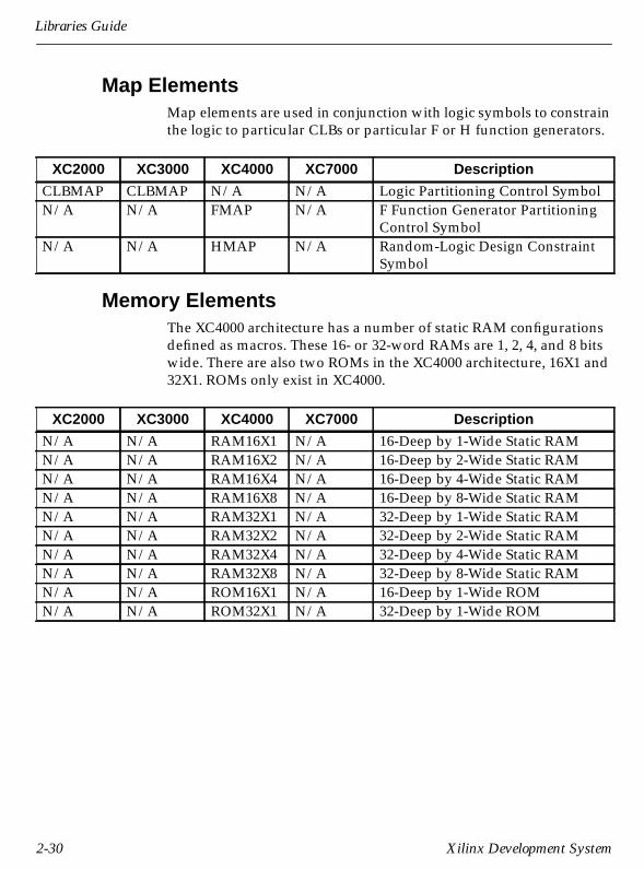
Libraries Guide
Map ElementsMap elements are used in conjunction with logic symbols to constrainthe logic to particular CLBs or particular F or H function generators.
Memory ElementsThe XC4000 architecture has a number of static RAM configurationsdefined as macros. These 16- or 32-word RAMs are 1, 2, 4, and 8 bitswide. There are also two ROMs in the XC4000 architecture, 16X1 and32X1. ROMs only exist in XC4000.
XC2000 XC3000 XC4000 XC7000 Description
CLBMAP CLBMAP N/A N/A Logic Partitioning Control SymbolN/A N/A FMAP N/A F Function Generator Partitioning
Control SymbolN/A N/A HMAP N/A Random-Logic Design Constraint
Symbol
XC2000 XC3000 XC4000 XC7000 Description
N/A N/A RAM16X1 N/A 16-Deep by 1-Wide Static RAMN/A N/A RAM16X2 N/A 16-Deep by 2-Wide Static RAMN/A N/A RAM16X4 N/A 16-Deep by 4-Wide Static RAMN/A N/A RAM16X8 N/A 16-Deep by 8-Wide Static RAMN/A N/A RAM32X1 N/A 32-Deep by 1-Wide Static RAMN/A N/A RAM32X2 N/A 32-Deep by 2-Wide Static RAMN/A N/A RAM32X4 N/A 32-Deep by 4-Wide Static RAMN/A N/A RAM32X8 N/A 32-Deep by 8-Wide Static RAMN/A N/A ROM16X1 N/A 16-Deep by 1-Wide ROMN/A N/A ROM32X1 N/A 32-Deep by 1-Wide ROM
2-30 Xilinx Development System

Selection Guide
MultiplexersThe multiplexer naming convention shown in the following figure,indicates the number of inputs and outputs and if an enable is avail-able. There are a number of TTL 7400-type multiplexers that haveactive-Low or inverted outputs.
Figure 2-7 Multiplexer Naming Convention
XC2000 XC3000 XC4000 XC7000 Description
M2_1 M2_1 M2_1 M2_1 2-to-1 MultiplexerM2_1B1 M2_1B1 M2_1B1 M2_1B1 2-to-1 Multiplexer with D0
InvertedM2_1B2 M2_1B2 M2_1B2 M2_1B2 2-to-1 Multiplexer with D0 and D1
InvertedM2_1E M2_1E M2_1E M2_1E 2-to-1 Multiplexer with EnableM4_1E M4_1E M4_1E M4_1E 4-to-1 Multiplexer with EnableM8_1E M8_1E M8_1E M8_1E 8-to-1 Multiplexer with EnableM16_1E M16_1E M16_1E M16_1E 16-to-1 Multiplexer with EnableX74_150 X74_150 X74_150 X74_150 16-to-1 Multiplexer with Active-
Low Enable and OutputX74_151 X74_151 X74_151 X74_151 8-to-1 Multiplexer with Active-
Low Enable and ComplementaryOutputs
X74_152 X74_152 X74_152 X74_152 8-to-1 Multiplexer with Active-Low Output
X74_153 X74_153 X74_153 X74_153 Dual 4-to-1 Multiplexer withActive-Low Enables and CommonSelect Input
X74_157 X74_157 X74_157 X74_157 Quadruple 2-to-1 Multiplexer withCommon Select and Active-LowEnable
X4620
M 8 _ 1 EMultiplexer
Number of Inputs
Number of Outputs
Output Enable
Libraries Guide 2-31

Libraries Guide
PLD ElementsPLD elements represent custom logic functions that are defined by anequation file in EPLD designs.
X74_158 X74_158 X74_158 X74_158 Quadruple 2-to-1 Multiplexer withCommon Select, Active-LowEnable, and Active-Low Outputs
X74_298 X74_298 X74_298 X74_298 Quadruple 2-Input Multiplexerwith Storage and Negative-EdgeClock
X74_352 X74_352 X74_352 X74_352 Dual 4-to-1 Multiplexer withActive-Low Enables and Outputs
XC2000 XC3000 XC4000 XC7000 Description
N/A N/A N/A PL20PIN Generic PLD Symbols for EPLDN/A N/A N/A PL24PINN/A N/A N/A PL48PINN/A N/A N/A PL20V8 20V8-Compatible PLD Symbol for
EPLDN/A N/A N/A PL22V10 22V10-Compatible PLD Symbol for
EPLDN/A N/A N/A PLFB9 EPLD High-Density Function
Block PLD SymbolN/A N/A N/A PLFFB9 EPLD Fast Function Block PLD
Symbol
XC2000 XC3000 XC4000 XC7000 Description
2-32 Xilinx Development System
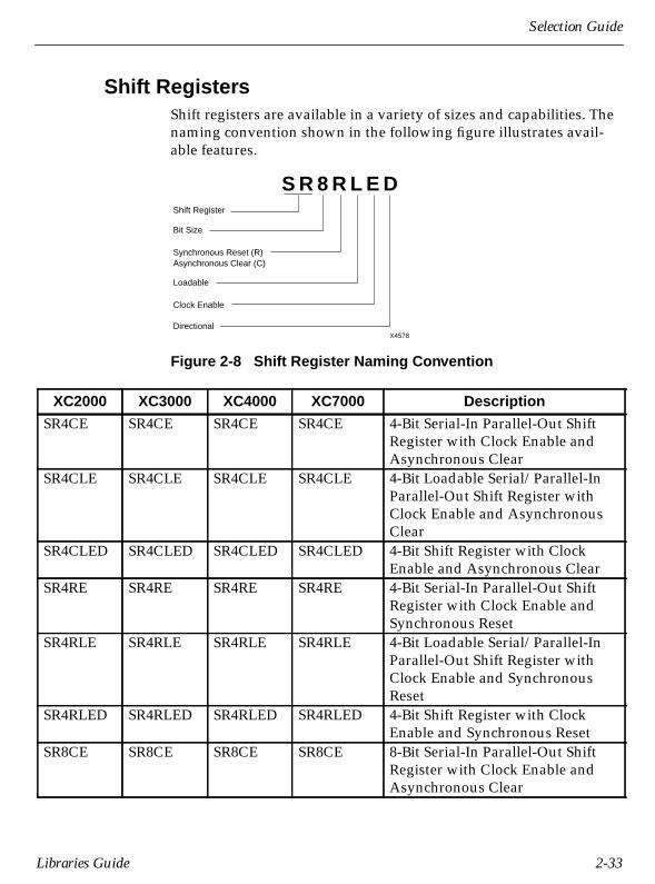
Selection Guide
Shift RegistersShift registers are available in a variety of sizes and capabilities. Thenaming convention shown in the following figure illustrates avail-able features.
Figure 2-8 Shift Register Naming Convention
XC2000 XC3000 XC4000 XC7000 Description
SR4CE SR4CE SR4CE SR4CE 4-Bit Serial-In Parallel-Out ShiftRegister with Clock Enable andAsynchronous Clear
SR4CLE SR4CLE SR4CLE SR4CLE 4-Bit Loadable Serial/Parallel-InParallel-Out Shift Register withClock Enable and AsynchronousClear
SR4CLED SR4CLED SR4CLED SR4CLED 4-Bit Shift Register with ClockEnable and Asynchronous Clear
SR4RE SR4RE SR4RE SR4RE 4-Bit Serial-In Parallel-Out ShiftRegister with Clock Enable andSynchronous Reset
SR4RLE SR4RLE SR4RLE SR4RLE 4-Bit Loadable Serial/Parallel-InParallel-Out Shift Register withClock Enable and SynchronousReset
SR4RLED SR4RLED SR4RLED SR4RLED 4-Bit Shift Register with ClockEnable and Synchronous Reset
SR8CE SR8CE SR8CE SR8CE 8-Bit Serial-In Parallel-Out ShiftRegister with Clock Enable andAsynchronous Clear
X4578
Bit Size
Shift Register
Asynchronous Clear (C)Synchronous Reset (R)
Clock Enable
Loadable
S R 8 R L E D
Directional
Libraries Guide 2-33

Libraries Guide
SR8CLE SR8CLE SR8CLE SR8CLE 8-Bit Loadable Serial/Parallel-InParallel-Out Shift Register withClock Enable and AsynchronousClear
SR8CLED SR8CLED SR8CLED SR8CLED 8-Bit Shift Register with ClockEnable and Asynchronous Clear
SR8RE SR8RE SR8RE SR8RE 8-Bit Serial-In Parallel-Out ShiftRegister with Clock Enable andSynchronous Reset
SR8RLE SR8RLE SR8RLE SR8RLE 8-Bit Loadable Serial/Parallel-InParallel-Out Shift Register withClock Enable and SynchronousReset
SR8RLED SR8RLED SR8RLED SR8RLED 8-Bit Shift Register with ClockEnable and Synchronous Reset
SR16CE SR16CE SR16CE SR16CE 16-Bit Serial-In Parallel-Out ShiftRegister with Clock Enable andAsynchronous Clear
SR16CLE SR16CLE SR16CLE SR16CLE 16-Bit Loadable Serial/Parallel-InParallel-Out Shift Register withClock Enable and AsynchronousClear
SR16CLED SR16CLED SR16CLED SR16CLED 16-Bit Shift Register with ClockEnable and Asynchronous Clear
SR16RE SR16RE SR16RE SR16RE 16-Bit Serial-In Parallel-Out ShiftRegister with Clock Enable andSynchronous Reset
SR16RLE SR16RLE SR16RLE SR16RLE 16-Bit Loadable Serial/Parallel-InParallel-Out Shift Register withClock Enable and SynchronousReset
SR16RLED SR16RLED SR16RLED SR16RLED 16-Bit Shift Register with ClockEnable and Synchronous Reset
X74_164 X74_164 X74_164 X74_164 8-Bit Serial-In Parallel-Out ShiftRegister with Active-Low Asyn-chronous Clear
XC2000 XC3000 XC4000 XC7000 Description
2-34 Xilinx Development System

Selection Guide
ShiftersShifters are barrel shifters (BRLSHFT) of four and eight bits.
Obsolete MacrosXilinx maintains software libraries with thousands of functionaldesign elements (primitives and macros) for different device architec-tures. When new elements are introduced that can provide additionalfunctions, greater flexibility, increased speed, or enhanced systemperformance, it is necessary to remove or replace existing elements.
In some cases, design elements in the following tables have beenobsoleted because their names changed to conform with the UnifiedLibraries’ naming conventions. In other cases, duplicate functionshave been eliminated. If you want a function that appears in thefollowing tables, and an exact or functionally similar replacementdoes not exist, check the appropriate functional table listed in theSelection Guide, earlier in this chapter to determine the appropriatecurrent macro.
X74_165S X74_165S X74_165S X74_165S 8-Bit Loadable Serial/Parallel-InParallel-Out Shift Register withClock Enable
X74_194 X74_194 X74_194 X74_194 4-Bit Loadable Directional Serial/Parallel-In Parallel-Out Shift Regis-ter
X74_195 X74_195 X74_195 X74_195 4-Bit Loadable Serial/Parallel-InParallel-Out Shift Register
XC2000 XC3000 XC4000 XC7000 Description
N/A BRLSHFT4 BRLSHFT4 BRLSHFT4 4-Bit Barrel ShifterN/A BRLSHFT8 BRLSHFT8 BRLSHFT8 8-Bit Barrel Shifter
XC2000 XC3000 XC4000 XC7000 Description
Libraries Guide 2-35

Libraries Guide
The Unified Libraries make certain types of elements obsolete for thefollowing reasons.
● Simple gates with names ending in B.
(Bs indicate inversion of all inputs) The gates are still available asoptions for the generic macro (for example, for AND3B, refer toAND).
● Some redundancies have been eliminated.
● Some macros have been eliminated because they were meaning-less inside an FPGA (for example, X74-240).
● Some macros have been eliminated because they were inefficientor had sub–optimal implementation.
If you have active designs that were created with former Xilinxlibraries’ primitives or macros, you may need to change references tothe design elements that you were using to reflect the new UnifiedLibraries elements.
The following tables list Unified Libraries exact replacements andsubstitutions for existing elements that you can use to update yourdesigns. Exact replacements are just that; you can use them forexactly the same function(s) as before. Substitutions provide at leastthe same functionality, but may afford additional advantages.Elements listed as obsolete are not recommended for new designs.They can still be found in some macro libraries, but support for themis being discontinued.
The elements are listed in alphanumeric order by architecture.Previous library element names appear in the left-most columnfollowed by their exact Unified Libraries’ replacement, if available. Ifan exact replacement does not exist, the closest substitution/anelement with similar functions is provided in the third column. If youare not sure of the function provided by an exact replacement orsubstitution, refer to the Selection Guide, earlier in this chapter.Macro functions that are no longer supported are indicated in theObsolete column.
2-36 Xilinx Development System

Selection Guide
XC2000 Replacement and Obsolete Macro Functions
ExistingXC2000Name
ExactUnified
Replacement
ClosestUnified
ReplacementObsolete
ASHEET ASHEETPBPAD IOPADBSHEET BSHEETLC2BCR CB2REC2BCRD CB2CEC2BP CB2CLEC2BR CB2REC2BRD CB2CLEC4BCP CB4CLEC4BCR CB2REC4BCRD CB2CEC4JCR CJ4REC6JCR CJ4REC8BCP CB4CLEC8BCR CB4REC8BCRD CB4CLEC8JCR CJ4REC10BCPRD CD4CLEC10BCRD CD4CEC10BPRD CD4CLEC10JCR CJ5REC12JCR CJ8REC16BARD CB4CEC16BCPR CB4CLEC16BCPRD CB4CLEC16BCRD CB4CEC16BPRD CB4CLEC16BUDRD CB4CLED
Libraries Guide 2-37

Libraries Guide
C16JCR CJ8REC256FCRD CB8CLEDCSHEET CSHEETLD2-4 D2_4ED2-4E D2_4ED3-8 D3_8ED3-8E D3_8EDFF FDDLAT LDCPDSHEET DSHEETLESHEET ESHEETLFDC FDCEFDCR FDREFDCS FDSEFDM ObsoleteFDMR ObsoleteFDMRD ObsoleteFDMS ObsoleteFDMSD ObsoleteFDRD FDCFDSD FDCPFDSRD FDCPFJK FJKCFJKRD FJKCFJKS FJKSREFJKSD FJKCPFJKSRD FJKCPFRS ObsoleteFSR ObsoleteFT FTC
ExistingXC2000Name
ExactUnified
Replacement
ClosestUnified
ReplacementObsolete
2-38 Xilinx Development System

Selection Guide
FT0 FTCFT0R FTRSEFT2 FTCEFT2R FTRSEFTP FTCPFTPRD FTRSLEFTR FTSREFTRD FTCFTS FTSREGADD ADD1GCOMP COMP2GEQGT ObsoleteGMAJ ObsoleteGMUX M2_1GOSC ObsoleteGPAR ObsoleteGXOR XOR2GXOR2 ObsoleteINFF IFDLDM ObsoleteLDMRD ObsoleteLDMSD ObsoleteLDRD LDCLDSD LDPLDSRD LDCPM3-1 M4_1M3-1E M4_1EM4-1 M4_1M4-1E M4_1EM8-1 M8_1
ExistingXC2000Name
ExactUnified
Replacement
ClosestUnified
ReplacementObsolete
Libraries Guide 2-39

Libraries Guide
M8-1E M8_1ENDFF ObsoleteOBUFZ OBUFTOUTFF OFDPAD IOPADPAL2RA10 ObsoletePAL6L16A ObsoletePAL8L14A ObsoletePAL10H8 ObsoletePAL10H20 ObsoletePAL10L8 ObsoletePAL12H6 ObsoletePAL12L6 ObsoletePAL12L10 ObsoletePAL14H4 ObsoletePAL14L4 ObsoletePAL14L8 ObsoletePAL16A4 ObsoletePAL16C1 ObsoletePAL16H2 ObsoletePAL16L2 ObsoletePAL16L6 ObsoletePAL16L8 ObsoletePAL16P8 ObsoletePAL16P8A ObsoletePAL16R4 ObsoletePAL16R4A ObsoletePAL16R6 ObsoletePAL16R6A ObsoletePAL16R8 Obsolete
ExistingXC2000Name
ExactUnified
Replacement
ClosestUnified
ReplacementObsolete
2-40 Xilinx Development System

Selection Guide
PAL16R8A ObsoletePAL16X4 ObsoletePAL16RA8 ObsoletePAL16RP4 ObsoletePAL16RP6 ObsoletePAL16RP8 ObsoletePAL18L4 ObsoletePAL20C1 ObsoletePAL20L2 ObsoletePAL20L8 ObsoletePAL20L10 ObsoletePAL20R4 ObsoletePAL20R6 ObsoletePAL20R8 ObsoletePAL20R10 ObsoletePAL20RS4 ObsoletePAL20RS8 ObsoletePAL20S10 ObsoletePAL20X4 ObsoletePAL20X8 ObsoletePAL20X10 ObsoletePAL22RX8 ObsoletePAL22V10 ObsoletePAL32R16 ObsoletePAL32V10 ObsoletePAL64R32 ObsoleteRD4 FD4RERD8 FD8CERD8CR FD8RERS4 SR4CE
ExistingXC2000Name
ExactUnified
Replacement
ClosestUnified
ReplacementObsolete
Libraries Guide 2-41

Libraries Guide
RS8 SR8CERS8CR SR8RERS8PR SR8RLERS8R SR8REZMX2000 ObsoleteZXPAL ObsoleteZX2000 Obsolete74-42 X74_4274-138 X74_13874-139 X74_13974-151 X74_15174-152 X74_15274-160 X74_16074-161 X74_16174-164 X74_16474-194 X74_19474-195 X74_19574-352 X74_352
ExistingXC2000Name
ExactUnified
Replacement
ClosestUnified
ReplacementObsolete
2-42 Xilinx Development System

Selection Guide
XC3000 Replacement and Obsolete Macro Functions
ExistingXC3000Name
ExactUnified
Replacement
ClosestUnified
ReplacementObsolete
ASHEET ASHEETPBPAD IOPADBRM ObsoleteBRM2 ObsoleteBSHEET BSHEETLCBINRIP ObsoleteCDECRIP CD4CECSHEET CSHEETLC2BCP ObsoleteC2BCPRD CB2CLEC2BCR CB2REC2BCRD CB2CEC2BP CB2CLEC2BR CB2REC2BRD CB2CLEC3BIT8 ObsoleteC3BIT8O7 ObsoleteC3SQUARE ObsoleteC4BCP CB4CLEC4BCPRD CB2CLEC4BCR CB2REC4BCRD CB2CEC4JX CJ4CEC4JXC CJ4CEC4JXCR CJ4REC4JXCRD CJ4CEC4JXRD CJ4CEC5BIT32 Obsolete
Libraries Guide 2-43

Libraries Guide
C5SQUARE ObsoleteC6JCR CJ4REC8BCP CB4CLEC8BCPRD CB4CLEC8BCR CB4REC8BCRD CB4CLEC8JCR CJ4REC8UDLD ObsoleteC10BCPRD CD4CLEC10BCRD CD4CEC10BPRD CD4CLEC10JCR CJ5REC12JCR CJ8REC16BARD CB4CEC16BCP CB4CLEC16BCPR CB4CLEC16BCPRD CB4CLEC16BCRD CB4CEC16BPRD CB4CLEC16BUDRD CB4CLEDC16DNLD CB4CLEDC16JCR CJ8REC16UDLD CB4CLEDC16UPLD CB4CLEDC256BCP CB8CLEC256BCPR CB8CLEC256BCR CB8REC256BCRD CB8CEC256FCRD CB8CLEDDFF FD
ExistingXC3000Name
ExactUnified
Replacement
ClosestUnified
ReplacementObsolete
2-44 Xilinx Development System

Selection Guide
DSHEET DSHEETLD2-4 D2_4ED2-4E D2_4ED3-8 D3_8ED3-8E D3_8EESHEET ESHEETLFDC FDCEFDCR FDREFDCRD FDCEFDCS FDSEFDM ObsoleteFDMR ObsoleteFDMRD ObsoleteFDMS ObsoleteFDRD FDCFJK FJKCFJKRD FJKCFJKS FJKSREFRS ObsoleteFSR ObsoleteFT FTCFT0 FTCFT0R FTRSEFTP FTCPFTPRD FTRSLEFTRD FTCFTS FTSREGADD ADD1GCOMP COMP2GLTGT COMPM2
ExistingXC3000Name
ExactUnified
Replacement
ClosestUnified
ReplacementObsolete
Libraries Guide 2-45

Libraries Guide
GMUX M2_1GOSC ObsoleteHX42 X74_42HX48 ObsoleteHX77 ObsoleteHX125 ObsoleteHX138 X74_138HX139 X74_139HX147 X74_147HX148 X74_148HX151 X74_151HX152 X74_152HX153 X74_153HX154 X74_154HX157 X74_157HX158 X74_158HX160 X74_160HX161 X74_161HX162 X74_162HX163 X74_163HX164 X74_164HX166 ObsoleteHX168 X74_168HX169 ObsoleteHX174 X74_174HX179 ObsoleteHX194 X74_194HX195 X74_195HX198 ObsoleteHX199 Obsolete
ExistingXC3000Name
ExactUnified
Replacement
ClosestUnified
ReplacementObsolete
2-46 Xilinx Development System

Selection Guide
HX240 ObsoleteHX241 ObsoleteHX244 ObsoleteHX257 ObsoleteHX258 ObsoleteHX259 ObsoleteHX273 X74_273HX278 ObsoleteHX280 X74_280HX283 X74_283HX298 X74_298HX352 X74_352HX373 ObsoleteHX374 ObsoleteHX377 X74_377HX390 X74_390HX393 ObsoleteHX518 X74_518HX521 X74_521HX541 ObsoleteHX577 ObsoleteHX590 ObsoleteHX595 ObsoleteINFF IFDINLAT ILDM3-1 M4_1M3-1E M4_1EM4-1 M4_1M4-1C ObsoleteM4-1E M4_1E
ExistingXC3000Name
ExactUnified
Replacement
ClosestUnified
ReplacementObsolete
Libraries Guide 2-47

Libraries Guide
M4-2 M2_1M8-1 M8_1M8-1E M8_1EOBUFZ OBUFTOUTFF OFDOUTFFT OFDTOUTFFZ OFDTPAD IOPADPAL2RA10 ObsoletePAL6L16A ObsoletePAL8L14A ObsoletePAL10H8 ObsoletePAL10H20 ObsoletePAL10L8 ObsoletePAL12H6 ObsoletePAL12L6 ObsoletePAL12L10 ObsoletePAL14H4 ObsoletePAL14L4 ObsoletePAL14L8 ObsoletePAL16A4 ObsoletePAL16C1 ObsoletePAL16H2 ObsoletePAL16L2 ObsoletePAL16L6 ObsoletePAL16L8 ObsoletePAL16P8 ObsoletePAL16P8A ObsoletePAL16RA8 ObsoletePAL16RP4 Obsolete
ExistingXC3000Name
ExactUnified
Replacement
ClosestUnified
ReplacementObsolete
2-48 Xilinx Development System
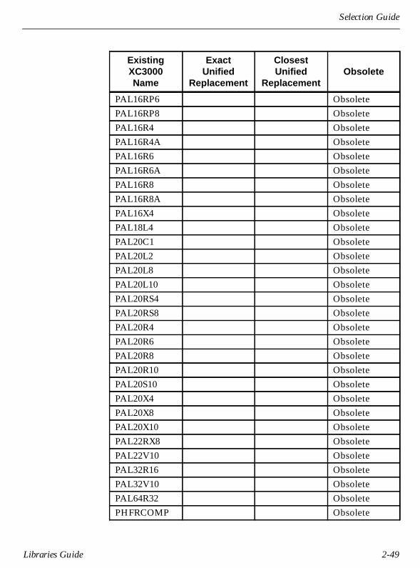
Selection Guide
PAL16RP6 ObsoletePAL16RP8 ObsoletePAL16R4 ObsoletePAL16R4A ObsoletePAL16R6 ObsoletePAL16R6A ObsoletePAL16R8 ObsoletePAL16R8A ObsoletePAL16X4 ObsoletePAL18L4 ObsoletePAL20C1 ObsoletePAL20L2 ObsoletePAL20L8 ObsoletePAL20L10 ObsoletePAL20RS4 ObsoletePAL20RS8 ObsoletePAL20R4 ObsoletePAL20R6 ObsoletePAL20R8 ObsoletePAL20R10 ObsoletePAL20S10 ObsoletePAL20X4 ObsoletePAL20X8 ObsoletePAL20X10 ObsoletePAL22RX8 ObsoletePAL22V10 ObsoletePAL32R16 ObsoletePAL32V10 ObsoletePAL64R32 ObsoletePHFRCOMP Obsolete
ExistingXC3000Name
ExactUnified
Replacement
ClosestUnified
ReplacementObsolete
Libraries Guide 2-49

Libraries Guide
RD4 FD4RERD4RD FD4RERD8 FD8CERD8CR FD8RERD8RD FD8RERS4 SR4CERS4C SR4CERS4CR SR4RERS4CRD SR4CERS4RD SR4RERS8 SR8CERS8C SR8CERS8CR SR8RERS8CRD SR8CERS8PR SR8RLERS8R SR8RERS8RD SR8RESAR ObsoleteTBUF BUFTWM8-1 ObsoleteWM16-1 ObsoleteX74160D ObsoleteX74160U X74_160X74161D ObsoleteX74161U X74_161X74165A X74_165SX74165S X74_165SX7474 FDCPZMX3000 ObsoleteZX3000 Obsolete
ExistingXC3000Name
ExactUnified
Replacement
ClosestUnified
ReplacementObsolete
2-50 Xilinx Development System

Selection Guide
ZXPAL ObsoleteZXTTL Obsolete74-42 X74_4274-138 X74_13874-139 X74_13974-151 X74_15174-152 X74_15274-160 X74_16074-161 X74_16174-162 X74_16274-163 X74_16374-164 X74_16474-194 X74_19474-195 X74_19574-352 X74_352
ExistingXC3000Name
ExactUnified
Replacement
ClosestUnified
ReplacementObsolete
Libraries Guide 2-51

Libraries Guide
XC4000 Replacement and Obsolete Macro Functions
ExistingXC4000Name
ExactUnified
Replacement
ClosestUnified
ReplacementObsolete
ACC8H ACC8ACC16H ACC16ADD1 ADD4ADD2 ADD4ADD12 ADD16ADD24 ObsoleteADD32 ObsoleteADDSUB1 ADSU4ADSU8H ADSU8ADSU16H ADSU16ASHEET ASHEETPBIDI4 ObsoleteBIDI8 ObsoleteBIDI16 ObsoleteBPAD IOPADBSHEET BSHEETLCDECRIP CD4CECOMP8H COMP8COMP16H COMP16COMP32 ObsoleteCOMPM8H COMPMC8COMPM16H COMPMC16COMPM32 ObsoleteCSHEET CSHEETLCUP8H CB8CLECUP16H CB16CLEC2BCPRD CB2CLEC2BCR CB2RE
2-52 Xilinx Development System

Selection Guide
C2BCRD CB2CEC2BINRIP CB2CEC4BCPRD CB2CLEC4BCR CB2REC4BCRD CB2CEC4BINRIP CB4CEC4JXCR CJ4REC4JXCRD CJ4CEC8BCPRD CB4CLEC8BCR CB4REC8BCRD CB4CLEC8JCR CJ4REC8JCRD CJ4CEC10BCPRD CD4CLEC10BCRD CD4CEC10JCR CJ5REC10JCRD CJ5CEC16BCPRD CB4CLEC16BCR CB4REC16BCRD CB4CEC16BUDRD CB4CLEDC16JCR CJ8REC16JCRD CJ8CEC32BUDRD CB8CLEDC64BUDRD CB8CLEDC256BCPR CB8CLEC256BCR CB8REC256BCRD CB8CEDEC2-4EH X74_139DEC3-8EH X74_138
ExistingXC4000Name
ExactUnified
Replacement
ClosestUnified
ReplacementObsolete
Libraries Guide 2-53

Libraries Guide
DECODE24 ObsoleteDSHEET DSHEETLD2-4 D2_4ED2-4E D2_4ED3-8 D3_8ED3-8E D3_8ED4-16 ObsoleteD4-16E D4_16ED7SEGH ObsoleteD7SEGMH ObsoleteENCPR8H X74_148ESHEET ESHEETLFDCR FDREFDCS FDSEFDMRD ObsoleteFDMSD ObsoleteFDRD FDCEFDRDKN FDCE_1FDSD FDPEFDSDKN FDPE_1FJKRD FJKCEFJKSD FJKPEFRD FDRSEFSD FDRSEFTPRD FTRSLEIN4 IBUF4IN8 IBUF8IN16 IBUF16INFF IFDINFF4 IFD4
ExistingXC4000Name
ExactUnified
Replacement
ClosestUnified
ReplacementObsolete
2-54 Xilinx Development System

Selection Guide
INFF8 IFD8INFF16 IFD16INFFS IFDIINLAT ILDINLAT4 ILD4INLAT8 ILD8INLAT16 ILD16INLATS ILDIINREG ObsoleteINREGS ObsoleteLD ObsoleteLDE ObsoleteLDM ObsoleteLDRD ObsoleteLDSD ObsoleteLRS ObsoleteLSR ObsoleteMAJ4 ObsoleteMUX4-1H M4_1MUX8-1H M8_1MUX16-1H M16_1M2-1 M2_1M2-1E M2_1EM4-1 M4_1M4-1E M4_1EM8-1 M8_1M8-1E M8_1EM16-1 M16_1M16-1E M16_1EOUT4 OBUF4
ExistingXC4000Name
ExactUnified
Replacement
ClosestUnified
ReplacementObsolete
Libraries Guide 2-55

Libraries Guide
OUT8 OBUF8OUT16 OBUF16OUTFF OFDOUTFF4 OFD4OUTFF8 OFD8OUTFF16 OFD16OUTFFS OFDTOUTFFT OFDTOUTFFTS OFDTPAD IOPADPADU UPADPAL2RA10 ObsoletePAL6L16A ObsoletePAL8L14A ObsoletePAL10H8 ObsoletePAL10H20 ObsoletePAL10L8 ObsoletePAL12H6 ObsoletePAL12L6 ObsoletePAL12L10 ObsoletePAL14H4 ObsoletePAL14L4 ObsoletePAL14L8 ObsoletePAL16A4 ObsoletePAL16C1 ObsoletePAL16H2 ObsoletePAL16L2 ObsoletePAL16L6 ObsoletePAL16L8 ObsoletePAL16P8 Obsolete
ExistingXC4000Name
ExactUnified
Replacement
ClosestUnified
ReplacementObsolete
2-56 Xilinx Development System

Selection Guide
PAL16P8A ObsoletePAL16R4 ObsoletePAL16R4A ObsoletePAL16R6 ObsoletePAL16R6A ObsoletePAL16R8 ObsoletePAL16R8A ObsoletePAL16RA8 ObsoletePAL16RP4 ObsoletePAL16RP6 ObsoletePAL16RP8 ObsoletePAL16X4 ObsoletePAL18L4 ObsoletePAL20C1 ObsoletePAL20L2 ObsoletePAL20L8 ObsoletePAL20L10 ObsoletePAL20R4 ObsoletePAL20R6 ObsoletePAL20R8 ObsoletePAL20R10 ObsoletePAL20RS4 ObsoletePAL20RS8 ObsoletePAL20S10 ObsoletePAL20X4 ObsoletePAL20X8 ObsoletePAL20X10 ObsoletePAL22RX8 ObsoletePAL22V10 ObsoletePAL32R16 Obsolete
ExistingXC4000Name
ExactUnified
Replacement
ClosestUnified
ReplacementObsolete
Libraries Guide 2-57

Libraries Guide
PAL32V10 ObsoletePAL64R32 ObsoletePARE9H X74_280PARO9H X74_280PHFRCOMP ObsoletePRSC8-9 ObsoleteRAM64X4 RAM32X4RAM64X8 RAM32X8RAM128X4 RAM32X4RAM128X8 RAM32X8RD4 FD4CERD4R FD4RERD8 FD8CERD8H FD8RERD8R FD8RERD16 FD16CERD16H RAM16X1RD16R FD16RERF16X4 ObsoleteRF16X8 ObsoleteRF16X16 ObsoleteRF32X4 ObsoleteRF32X8 ObsoleteRF32X16 ObsoleteRM16X2H RAM16X2RM16X4H RAM16X4RM16X8H RAM16X8RM32X4H RAM32X4RM32X8H RAM32X8RM64X4H RAM32X4
ExistingXC4000Name
ExactUnified
Replacement
ClosestUnified
ReplacementObsolete
2-58 Xilinx Development System
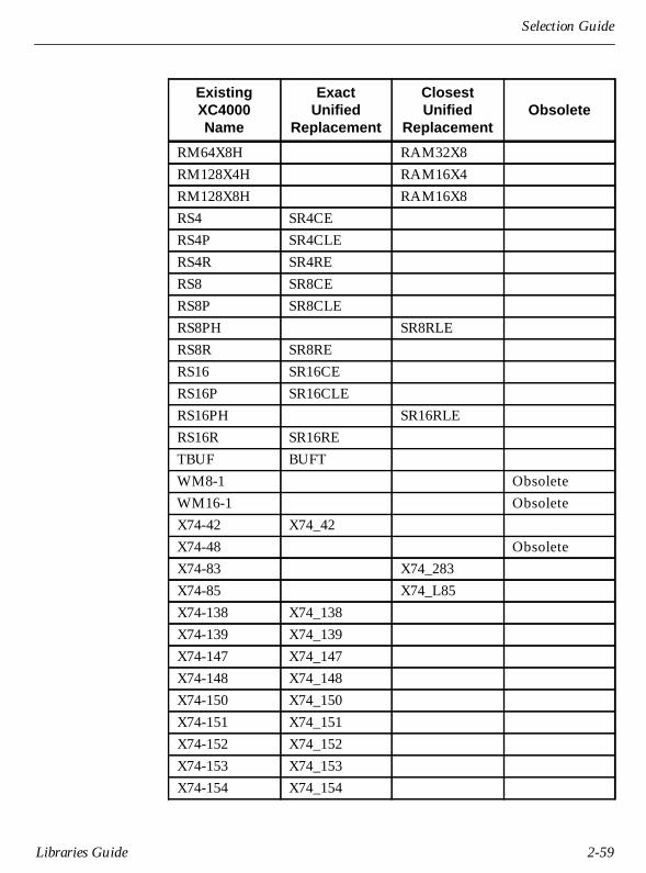
Selection Guide
RM64X8H RAM32X8RM128X4H RAM16X4RM128X8H RAM16X8RS4 SR4CERS4P SR4CLERS4R SR4RERS8 SR8CERS8P SR8CLERS8PH SR8RLERS8R SR8RERS16 SR16CERS16P SR16CLERS16PH SR16RLERS16R SR16RETBUF BUFTWM8-1 ObsoleteWM16-1 ObsoleteX74-42 X74_42X74-48 ObsoleteX74-83 X74_283X74-85 X74_L85X74-138 X74_138X74-139 X74_139X74-147 X74_147X74-148 X74_148X74-150 X74_150X74-151 X74_151X74-152 X74_152X74-153 X74_153X74-154 X74_154
ExistingXC4000Name
ExactUnified
Replacement
ClosestUnified
ReplacementObsolete
Libraries Guide 2-59
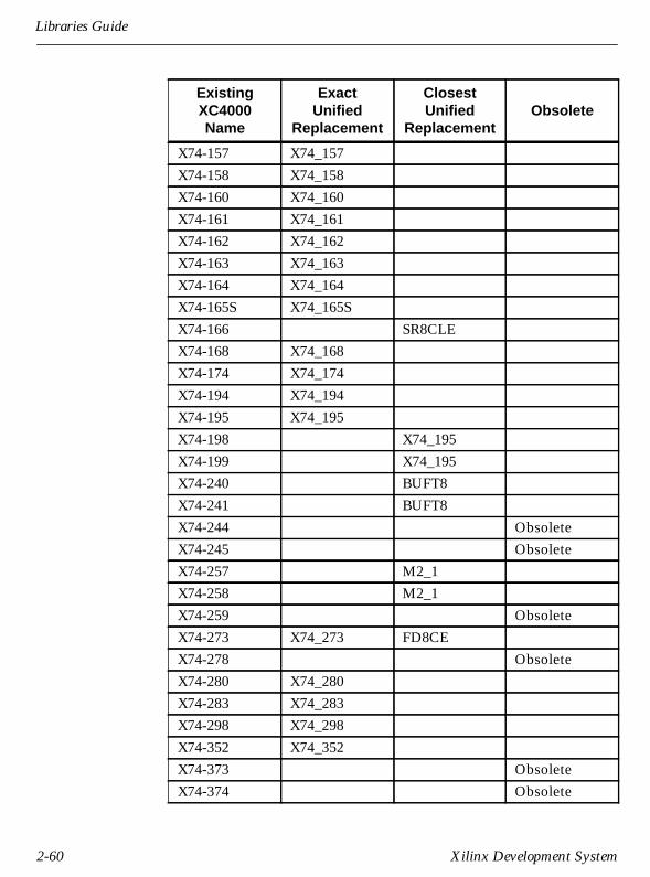
Libraries Guide
X74-157 X74_157X74-158 X74_158X74-160 X74_160X74-161 X74_161X74-162 X74_162X74-163 X74_163X74-164 X74_164X74-165S X74_165SX74-166 SR8CLEX74-168 X74_168X74-174 X74_174X74-194 X74_194X74-195 X74_195X74-198 X74_195X74-199 X74_195X74-240 BUFT8X74-241 BUFT8X74-244 ObsoleteX74-245 ObsoleteX74-257 M2_1X74-258 M2_1X74-259 ObsoleteX74-273 X74_273 FD8CEX74-278 ObsoleteX74-280 X74_280X74-283 X74_283X74-298 X74_298X74-352 X74_352X74-373 ObsoleteX74-374 Obsolete
ExistingXC4000Name
ExactUnified
Replacement
ClosestUnified
ReplacementObsolete
2-60 Xilinx Development System

Selection Guide
X74-377 X74_377X74-390 X74_390X74-518 X74_518X74-521 X74_521X74-540 ObsoleteX74-541 ObsoleteX74-577 ObsoleteX74-595 SR8CEX74160D X74_160X74160U X74_160X74161D X74_161X74161U X74_161X74_162 X74_163ZHM4000 ObsoleteZMX4000 ObsoleteZX4000 ObsoleteZXPAL Obsolete
ExistingXC4000Name
ExactUnified
Replacement
ClosestUnified
ReplacementObsolete
Libraries Guide 2-61

Libraries Guide
XC7000 Replacement and Obsolete Macro Functions
ExistingXC7000Name
ExactUnified
Replacement
ClosestUnified
ReplacementObsolete
PA7236A ObsoletePA7272A ObsoletePA7272B ObsoletePA7272C ObsoletePA73108A ObsoletePA73108B ObsoletePL00 NAND2PL02 NOR2PL04 INVPL08 AND2PL10 NAND3PL11 AND3PL20 NAND4PL21 AND4PL27 NOR3PL30 NAND8PL32 OR2PL74 FDCPPL74PZ FDPL76P FJKCPPL83 ADD4PL85 X74_L85PL86 XOR2PL126 BUFEPL138 X74_138PL139 X74_139PL148P X74_148PL150 X74_150PL151 X74_151
2-62 Xilinx Development System
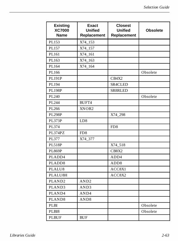
Selection Guide
PL153 X74_153PL157 X74_157PL161 X74_161PL163 X74_163PL164 X74_164PL166 ObsoletePL191P CB4X2PL194 SR4CLEDPL198P SR8RLEDPL240 ObsoletePL244 BUFT4PL266 XNOR2PL298P X74_298PL373P LD8PL374 FD8PL374PZ FD8PL377 X74_377PL518P X74_518PL869P CB8X2PLADD4 ADD4PLADD8 ADD8PLALU8 ACC8X1PLALU8H ACC8X2PLAND2 AND2PLAND3 AND3PLAND4 AND4PLAND8 AND8PLBI ObsoletePLBI8 ObsoletePLBUF BUF
ExistingXC7000Name
ExactUnified
Replacement
ClosestUnified
ReplacementObsolete
Libraries Guide 2-63

Libraries Guide
PLBUFT BUFEPLBUFT4 BUFT4PLCE BUFCEPLCEIO ObsoletePLCOMP8 COMP8PLCOMP8R ObsoletePLCTR4A X74_161PLCTR4S X74_163PLCTR8 CB8RLEPLCTR8T ObsoletePLDECOD2 X74_139PLDECOD3 X74_138PLDFF FDPLDFF8 FD8PLDFFE8 X74_377PLDFFEI IFDX1PLDFFEI8 IFD8X1PLDFFEIO ObsoletePLDFFI IFDPLDFFI8 IFD8PLDFFIO ObsoletePLDFFRSC FDCPPLDFFT8 FD8PLDLAT LDPLDLAT8 LD8PLDLATI ILDPLDLATI8 ILD8PLDLATIO ObsoletePLENCOD8 X74_148PLFCLKIO Obsolete
ExistingXC7000Name
ExactUnified
Replacement
ClosestUnified
ReplacementObsolete
2-64 Xilinx Development System

Selection Guide
PLFCOMP ObsoletePLFOE BUFFOEPLFOEIO ObsoletePLFPLA48 PL48PINPLFSTCLK BUFGPLIN IBUFPLIN8 IBUF8PLIN8A IBUF8PLIO ObsoletePLIO8 ObsoletePLJKFFC FJKCPPLMAG4 X74_L85PLMAG8 COMPM8PLMAG4R ObsoletePLMAG8R ObsoletePLMUX2 M2_1PLMUX4 M4_1EPLMUX8 X74_151PLMUX16 X74_150PLMUX2R4 X74_298PLMUX2X4 X74_157PLMUX4X2 X74_153PLNAND2 NAND2PLNAND3 NAND3PLNAND4 NAND4PLNAND8 NAND8PLNOR2 NOR2PLNOR3 NOR3PLNOR4 NOR4PLNOR8 NOR8
ExistingXC7000Name
ExactUnified
Replacement
ClosestUnified
ReplacementObsolete
Libraries Guide 2-65

Libraries Guide
PLNOT INVPLNOTT4 ObsoletePLOR2 OR2PLOR3 OR3PLOR4 OR4PLOR8 OR8PLOUT OBUFPLOUT8 OBUF8PLOUT8A OBUF8PLOUTT OBUFEX1PLOUTT8 OBUFE8X1PLPLD9 PLFB9PLPLD9F PLFFB9PLSHIF4 SR4RLEDPLSHIF4A SR4CLEDPLSHIF8 SR8RLEDPLSHIF8I X74_164PLSHIF8O ObsoletePLUPDN4 CB4X2PLUPDN8 CB8X2PLUPDN8T ObsoletePLXNOR2 XNOR2PLXOR2 XOR2PLXOR3 XOR3PLXOR4 XOR4PLXOR5 XOR5PLXOR6 XOR6PLXOR7 XOR7PLXOR8 XOR8PLXOR9 XOR9
ExistingXC7000Name
ExactUnified
Replacement
ClosestUnified
ReplacementObsolete
2-66 Xilinx Development System

Chapter 3
Libraries Guide — 0401410 01 3-1
Design ElementsThis chapter contains design elements for the XC2000, XC3000,XC4000, and XC7000 architectures. The elements are organized inalphanumeric order, with all numeric suffixes in ascending order.
ACC1
1-Bit Loadable Cascadable Accumulator withCarry-In, Carry-Out, and Synchronous Reset
* not supported for XC7272 or XC7336 designs
ACC1 can add or subtract a 1-bit unsigned-binary word to or fromthe contents of a 1-bit data register and store the results in theregister. The register can be loaded with a 1-bit word. The synchro-nous reset (R) has priority over all other inputs and, when High,causes the output to go to logic level zero. Clock (C) transitions areignored when clock enable (CE) is Low.
The accumulator is asynchronously reset, output Low, when power isapplied or when global reset, GR, is active (Low).
LoadWhen the load input (L) is High, CE is ignored and the data on theinput D0 is loaded into the 1-bit register.
XC2000 XC3000 XC4000 XC7000
Macro N/A N/A Primitive*
X3862
ACC1
C
D0
B0
CI Q0
CO
L
CE
ADD
R

Libraries Guide
AddWhen control inputs ADD and CE are both High, the accumulatoradds a 1-bit word (B0) and carry-in (CI) to the contents of the 1-bitregister. The result is stored in the register and appears on output Q0during the Low-to-High clock transition. The carry-out (CO) is notregistered synchronously with the data output. CO always reflectsthe accumulation of input B0 and the contents of the register, whichallows cascading of ACC1s by connecting CO of one stage to CI of thenext stage. In add mode, CO acts as a carry-out, and CO and CI areactive-High.
SubtractWhen ADD is Low and CE is High, the 1-bit word B0 and CI aresubtracted from the contents of the register. The result is stored in theregister and appears on output Q0 during the Low-to-High clocktransition. The carry-out (CO) is not registered synchronously withthe data output. CO always reflects the accumulation of input B0 andthe contents of the register, which allows cascading of ACC1s byconnecting CO of one stage to CI of the next stage. In subtract mode,CO acts as a borrow, and CO and CI are active-Low.
Figure 3-1 ACC1 XC2000 Implementation
R
CE
B0
C
R_L_CE
R_SD0
COADD
CI
D0
Q0
Q0SD0
L
S0
GND
SD0
D0
D1O
S0
M2_1
CI
COB0ADD
ADSU1
A0
S0
OR3
AND2B1
Q0
FDCE
QD
CLR
CE
C
3-2 Xilinx Development System

Design Elements
For the XC7000 EPLD architecture, the CO output is not valid duringload (L=High), during reset (R=High), or while CE is inactive (Low).Also, the CI and CO pins are not implemented using the EPLD arith-metic carry path and should be used to cascade accumulators. Referto “ACC1X1” and “ACC1X2” for descriptions of cascadable EPLDaccumulators.
Libraries Guide 3-3
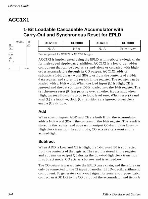
Libraries Guide
ACC1X1
1-Bit Loadable Cascadable Accumulator withCarry-Out and Synchronous Reset for EPLD
*not supported for XC7272 or XC7336 designs
ACC1X1 is implemented using the EPLD arithmetic carry-logic chainfor high-speed ripple-carry addition. ACC1X1 is a low-order addercomponent that can be used as a stand-alone or cascaded with high-order accumulators through its CO output. ACC1X1 adds orsubtracts a 1-bit binary word (B0) to or from the contents of a 1-bitdata register and stores the results in the register. The register can beloaded with a 1-bit word. When the load input (L) is High, CE isignored and the data on input D0 is loaded into the 1-bit register. Thesynchronous reset (R) has priority over all other inputs and, whenHigh, causes all outputs to go to logic level zero. When reset (R) andload (L) are inactive, clock (C) transitions are ignored when clockenable (CE) is Low.
AddWhen control inputs ADD and CE are both High, the accumulatoradds a 1-bit word (B0) to the contents of the 1-bit register. The result isstored in the register and appears on output Q0 during the Low-to-High clock transition. In add mode, CO acts as a carry-out and isactive-High.
SubtractWhen ADD is Low and CE is High, the 1-bit word B0 is subtractedfrom the contents of the register. The result is stored in the registerand appears on output Q0 during the Low-to-High clock transition.In subtract mode, CO acts as a borrow and is active-Low.
The CO output is passed into the EPLD carry chain, and therefore canonly be connected to the CI input of another EPLD-specific arithmeticcomponent. To generate a carry-out signal for general-purpose logic,connect an ADD1X2 to the CO output of the accumulator and tie its A
XC2000 XC3000 XC4000 XC7000
N/A N/A N/A Primitive*
X4240
ACC1X1
C
D0
B0
Q0
CO
L
CE
ADD
R
3-4 Xilinx Development System

Design Elements
and B inputs to GND; the S output becomes the carry-out. If a carry-in is required from general-purpose logic, use an ACC1X2 for theleast-significant accumulator and connect an ADD1X1 to its CI input.Then connect your carry-in signal to both the A and B inputs of theADD1X1 (the S output is not used) to generate a carry into the carrychain for the first bit of the accumulator. The accumulator register isinitialized to zero when powered is applied or when the deviceMaster Reset input is activated. The clock (C) input can be driven byeither the EPLD FastCLK global net (represented by a BUFG symbol),an ordinary input, or other on-chip logic.
d, q, b = state of referenced input one set-up time prior to active clock transition
Inputs Outputs
R L CE B0 D0 C ADD Q0 CO
1 X X X X ↑ X 0 00 1 X X D0 ↑ X d 00 0 0 X X X X No Chg 00 0 1 B0 X ↑ 1 q+b CO0 0 1 B0 X ↑ 0 q-b CO
Libraries Guide 3-5

Libraries Guide
ACC1X2
1-Bit Loadable Cascadable Accumulator withCarry-In, Carry-Out, and Synchronous Reset
* not supported for XC7272 or XC7336 designs
ACC1X2 is implemented using the EPLD arithmetic carry-logic chainfor high-speed ripple-carry addition. ACC1X2 is a high-order addercomponent cascaded to lower-order accumulators through its CIinput. ACC1X2 adds or subtracts a 1-bit binary word (B0) to or fromthe contents of a 1-bit data register and stores the results in theregister. The register can be loaded with a 1-bit word. When the loadinput (L) is High, CE is ignored and the data on input D0 is loadedinto the 1-bit register. The synchronous reset (R) has priority over allother inputs and, when High, causes all outputs to go to logic levelzero. When reset (R) and load (L) are inactive, clock (C) transitions areignored when clock enable (CE) is Low.
AddWhen control inputs ADD and CE are both High, the accumulatoradds a 1-bit word (B0) and carry-in (CI) to the contents of the 1-bitregister. The result is stored in the register and appears on output Q0during the Low-to-High clock transition. In add mode, CO acts as acarry-out, and CO and CI are active-High.
SubtractWhen ADD is Low and CE is High, the 1-bit word B0 and CI aresubtracted from the contents of the register. The result is stored in theregister and appears on output Q0 during the Low-to-High clocktransition. In subtract mode, CO acts as a borrow, and CO and CI areactive-Low.
The CI input is taken from the EPLD carry chain, and therefore, mustonly be connected to the CO output of another EPLD-specific arith-metic component. The CO output is passed into the EPLD carrychain, and can only be connected to the CI input of another
XC2000 XC3000 XC4000 XC7000
N/A N/A N/A Primitive*
X4241
ACC1X2
C
D0
B0
CI Q0
CO
L
CE
ADD
R
3-6 Xilinx Development System
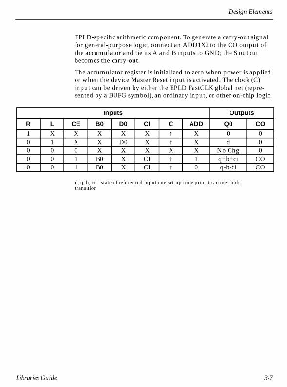
Design Elements
EPLD-specific arithmetic component. To generate a carry-out signalfor general-purpose logic, connect an ADD1X2 to the CO output ofthe accumulator and tie its A and B inputs to GND; the S outputbecomes the carry-out.
The accumulator register is initialized to zero when power is appliedor when the device Master Reset input is activated. The clock (C)input can be driven by either the EPLD FastCLK global net (repre-sented by a BUFG symbol), an ordinary input, or other on-chip logic.
d, q, b, ci = state of referenced input one set-up time prior to active clocktransition
Inputs Outputs
R L CE B0 D0 CI C ADD Q0 CO
1 X X X X X ↑ X 0 00 1 X X D0 X ↑ X d 00 0 0 X X X X X No Chg 00 0 1 B0 X CI ↑ 1 q+b+ci CO0 0 1 B0 X CI ↑ 0 q-b-ci CO
Libraries Guide 3-7

Libraries Guide
ACC4
4-Bit Loadable Cascadable Accumulator withCarry-In, Carry-Out, and Synchronous Reset
* not supported for XC7272 or XC7336 designs
ACC4 can add or subtract a 4-bit unsigned-binary or twos-comple-ment word to or from the contents of a 4-bit data register and storethe results in the register. The register can be loaded with a 4-bitword. In the XC4000 family, the accumulator is implemented usingcarry logic and relative location constraints, which assure most effi-cient logic placement. The synchronous reset (R) has priority over allother inputs, and when High, causes all outputs to go to logic levelzero. Clock (C) transitions are ignored when clock enable (CE) is Low.
The accumulator is asynchronously reset, output Low, when power isapplied or when global reset (GR for XC3000) or global set/reset(GSR for XC4000) is active. GR is active Low; the GSR active level isprogrammable.
LoadWhen the load input (L) is High, CE is ignored and the data on inputsD3 – D0 is loaded into the 4-bit register.
Unsigned Binary Versus Twos-ComplementACC4 can operate on either 4-bit unsigned binary numbers or 4-bittwos-complement numbers. If the inputs are interpreted as unsignedbinary, the result can be interpreted as unsigned binary. If the inputsare interpreted as twos complement, the output can be interpreted astwos complement. The only functional difference between anunsigned binary operation and a twos-complement operation is howthey determine when “overflow” occurs. Unsigned binary uses CO,while twos-complement uses OFL to determine when “overflow”occurs.
For the XC7000 EPLD architecture, the CO output is not valid duringload (L=High), during reset (R=High), or while CE is inactive (Low).
XC2000 XC3000 XC4000 XC7000
N/A Macro Macro Primitive*
X3863
ACC4
C
D3
D2
D1
Q3
CO
L
CE
ADD
D0
B0
CI
B1
B3
B2
OFL
Q1
Q2
Q0
R
3-8 Xilinx Development System
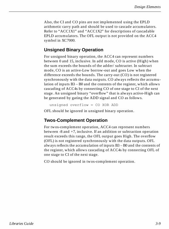
Design Elements
Also, the CI and CO pins are not implemented using the EPLDarithmetic carry path and should be used to cascade accumulators.Refer to “ACC1X1” and “ACC1X2” for descriptions of cascadableEPLD accumulators. The OFL output is not provided on the ACC4symbol in XC7000.
Unsigned Binary OperationFor unsigned binary operation, the ACC4 can represent numbersbetween 0 and 15, inclusive. In add mode, CO is active (High) whenthe sum exceeds the bounds of the adder/subtracter. In subtractmode, CO is an active-Low borrow-out and goes Low when thedifference exceeds the bounds. The carry-out (CO) is not registeredsynchronously with the data outputs. CO always reflects the accumu-lation of inputs B3 – B0 and the contents of the register, which allowscascading of ACC4s by connecting CO of one stage to CI of the nextstage. An unsigned binary “overflow” that is always active-High canbe generated by gating the ADD signal and CO as follows.
unsigned overflow = CO XOR ADD
OFL should be ignored in unsigned binary operation.
Twos-Complement OperationFor twos-complement operation, ACC4 can represent numbersbetween -8 and +7, inclusive. If an addition or subtraction operationresult exceeds this range, the OFL output goes High. The overflow(OFL) is not registered synchronously with the data outputs. OFLalways reflects the accumulation of inputs B3 – B0 and the contents ofthe register, which allows cascading of ACC4s by connecting OFL ofone stage to CI of the next stage.
CO should be ignored in twos-complement operation.
Libraries Guide 3-9

Libraries Guide
XC4000 Topology
X3662
Q 3
CO
OFL
Q 2
Q 1
Q 0
B 3A 3
B 2A 2
B 1A 1
B 0A 0
CI
3-10 Xilinx Development System

Design Elements
ACC4X1
4-Bit Loadable Cascadable Accumulator withCarry-Out and Synchronous Reset for EPLD
* not supported for XC7272 or XC7336 designs
ACC4X1 is implemented using the EPLD arithmetic carry-logic chainfor high-speed ripple-carry addition. ACC4X1 is a low-order addercomponent, which can be used as a stand-alone or cascaded withhigh-order accumulators through its CO output. ACC4X1 adds orsubtracts a 4-bit binary word (B3 – B0) to or from the contents of a4-bit data register and stores the results in the register. The registercan be loaded with a 4-bit word. When the load input (L) is High, CEis ignored and the data on inputs D3 – D0 is loaded into the 4-bitregister. The synchronous reset (R) has priority over all other inputsand, when High, causes all outputs to go to logic level zero. Whenreset (R) and load (L) are inactive, clock (C) transitions are ignoredwhen clock enable (CE) is Low.
AddWhen control inputs ADD and CE are both High, the accumulatoradds a 4-bit word (B3 – B0) to the contents of the 4-bit register. Theresult is stored in the register and appears on outputs Q3 – Q0 duringthe Low-to-High clock transition. In add mode, CO acts as a carry-out and is active-High.
SubtractWhen ADD is Low and CE is High, the 4-bit word B3 – B0 issubtracted from the contents of the register. The result is stored in theregister and appears on outputs Q3 – Q0 during the Low-to-Highclock transition. In subtract mode, CO acts as a borrow and is active-Low.
The CO output is passed into the EPLD carry chain, and therefore canonly be connected to the CI input of another EPLD-specific arithmeticcomponent. To generate a carry-out signal for general-purpose logic,
XC2000 XC3000 XC4000 XC7000
N/A N/A N/A Primitive*
X4244
ACC4X1
C
D3
D2
D1
Q3
CO
L
CE
ADD
D0
B0
B1
B3
B2
Q1
Q2
Q0
R
Libraries Guide 3-11

Libraries Guide
connect an ADD1X2 to the CO output of the accumulator and tie its Aand B inputs to GND; the S output becomes the carry-out. If acarry-in is required from general-purpose logic, use an ACC4X2 forthe least-significant accumulator and connect an ADD1X1 to its CIinput. Then connect your carry-in signal to both the A and B inputs ofthe ADD1X1 (the S output is not used) to generate a carry into thecarry chain for the first bit of the accumulator.
The accumulator register is initialized to zero when power is appliedor when the device Master Reset pin is activated. The clock (C) inputcan be driven by either the EPLD FastCLK global net (represented bya BUFG symbol), an ordinary input, or other on-chip logic.
Refer to “ACC1X1” for truth table derivation.
3-12 Xilinx Development System

Design Elements
ACC4X2
4-Bit Loadable Cascadable Accumulator withCarry-In, Carry-Out, and Synchronous Reset
* not supported for XC7272 or XC7336 designs
ACC4X2 is implemented using the EPLD arithmetic carry-logic chainfor high-speed ripple-carry addition. ACC4X2 is a high-order addercomponent cascaded to lower-order accumulators through its CIinput. ACC4X2 adds or subtracts a 4-bit binary word (B3 – B0) to orfrom the contents of a 4-bit data register and stores the results in theregister. The register can be loaded with a 4-bit word. When the loadinput (L) is High, CE is ignored and the data on inputs D3 – D0 isloaded into the 4-bit register. The synchronous reset (R) has priorityover all other inputs and, when High, causes all outputs to go to logiclevel zero. When reset (R) and load (L) are inactive, clock (C) transi-tions are ignored when clock enable (CE) is Low.
AddWhen control inputs ADD and CE are both High, the accumulatoradds a 4-bit word (B3 – B0) and carry-in (CI) to the contents of the4-bit register. The result is stored in the register and appears onoutputs Q3 – Q0 during the Low-to-High clock transition. In addmode, CO acts as a carry-out, and CO and CI are active-High.
SubtractWhen ADD is Low and CE is High, the 4-bit word B3 – B0 and CI aresubtracted from the contents of the register. The result is stored in theregister and appears on outputs Q3 – Q0 during the Low-to-Highclock transition. In subtract mode, CO acts as a borrow, and CO andCI are active-Low.
The CI input is taken from the EPLD carry chain, and therefore mustonly be connected to the CO output of another EPLD-specific arith-metic component. The CO output is passed into the EPLD carry chainand can only be connected to the CI input of another EPLD-specific
XC2000 XC3000 XC4000 XC7000
N/A N/A N/A Primitive*
X4245
ACC4X2
C
D3
D2
D1
Q3
CO
L
CE
ADD
D0
B0
CI
B1
B3
B2
Q1
Q2
Q0
R
Libraries Guide 3-13

Libraries Guide
arithmetic component. To generate a carry-out signal for general-purpose logic, connect an ADD1X2 to the CO output of the accumu-lator and tie its A and B inputs to GND; the S output becomes thecarry-out.
The accumulator register is initialized to zero when power is appliedor when the device Master Reset pin is activated. The clock (C) inputcan be driven by either the EPLD FastCLK global net (represented bya BUFG symbol), an ordinary input, or other on-chip logic.
Refer to “ACC1X2” for truth table derivation.
3-14 Xilinx Development System

Design Elements
ACC8
8-Bit Loadable Cascadable Accumulator withCarry-In, Carry-Out, and Synchronous Reset
* not supported for XC7272 or XC7336 designs
ACC8 can add or subtract an 8-bit unsigned-binary or twos- comple-ment word to or from the contents of an 8-bit data register and storethe results in the register. The register can be loaded with an 8-bitword. In the XC4000 family, the accumulator is implemented usingcarry logic and relative location constraints, which assure most effi-cient logic placement. The synchronous reset (R) has priority over allother inputs, and when High, causes all outputs to go to logic levelzero. Clock (C) transitions are ignored when clock enable (CE) is Low.
The accumulator is asynchronously reset, output Low, when power isapplied or when global reset (GR for XC3000) or global set/reset(GSR for XC4000) is active. GR is active Low; the GSR active level isprogrammable.
LoadWhen the load input (L) is High, CE is ignored and the data on inputsD7 – D0 is loaded into the 8-bit register.
Unsigned Binary Versus Twos-ComplementACC8 can operate on either 8-bit unsigned binary numbers or 8-bittwos-complement numbers. If the inputs are interpreted as unsignedbinary, the result can be interpreted as unsigned binary. If the inputsare interpreted as twos complement, the output can be interpreted astwos complement. The only functional difference between anunsigned binary operation and a twos-complement operation is howthey determine when “overflow” occurs. Unsigned binary uses CO,while twos-complement uses OFL to determine when “overflow”occurs.
For the XC7000 EPLD architecture, the CO output is not valid duringload (L=High), during reset (R=High), or while CE is inactive (Low).
XC2000 XC3000 XC4000 XC7000
N/A Macro Macro Macro*
X4374
ACC8
C
D[7:0]
B[7:0]
CI
L
CE
ADD
R
CO
Q[7:0]
OFL
Libraries Guide 3-15
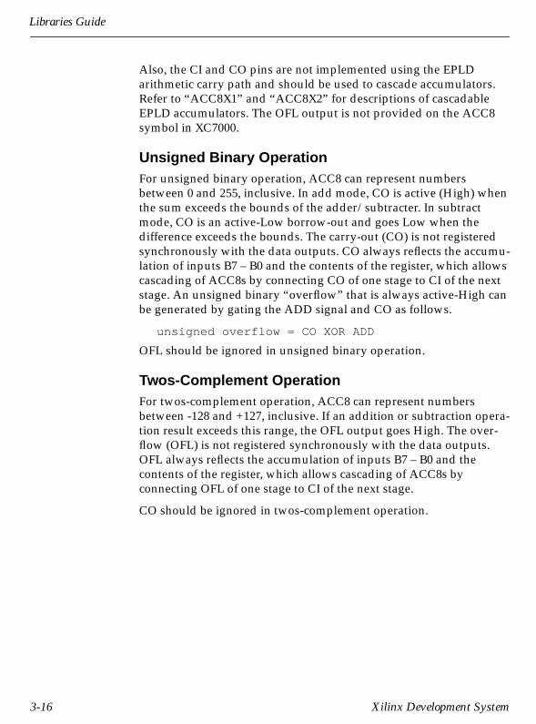
Libraries Guide
Also, the CI and CO pins are not implemented using the EPLDarithmetic carry path and should be used to cascade accumulators.Refer to “ACC8X1” and “ACC8X2” for descriptions of cascadableEPLD accumulators. The OFL output is not provided on the ACC8symbol in XC7000.
Unsigned Binary OperationFor unsigned binary operation, ACC8 can represent numbersbetween 0 and 255, inclusive. In add mode, CO is active (High) whenthe sum exceeds the bounds of the adder/subtracter. In subtractmode, CO is an active-Low borrow-out and goes Low when thedifference exceeds the bounds. The carry-out (CO) is not registeredsynchronously with the data outputs. CO always reflects the accumu-lation of inputs B7 – B0 and the contents of the register, which allowscascading of ACC8s by connecting CO of one stage to CI of the nextstage. An unsigned binary “overflow” that is always active-High canbe generated by gating the ADD signal and CO as follows.
unsigned overflow = CO XOR ADD
OFL should be ignored in unsigned binary operation.
Twos-Complement OperationFor twos-complement operation, ACC8 can represent numbersbetween -128 and +127, inclusive. If an addition or subtraction opera-tion result exceeds this range, the OFL output goes High. The over-flow (OFL) is not registered synchronously with the data outputs.OFL always reflects the accumulation of inputs B7 – B0 and thecontents of the register, which allows cascading of ACC8s byconnecting OFL of one stage to CI of the next stage.
CO should be ignored in twos-complement operation.
3-16 Xilinx Development System

Design Elements
XC4000 Topology
X3663
Q 7
CO
OFL
Q 6
Q 5
Q 4
B 7A 7
B 6A 6
B 5A 5
B 4A 4
CI
Q 3
Q 2
Q 1
Q 0
B 3A 3
B 2A 2
B 1A 1
B 0A 0
Libraries Guide 3-17
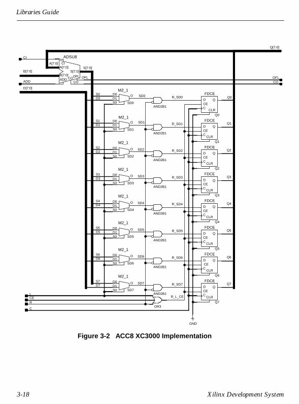
Libraries Guide
Figure 3-2 ACC8 XC3000 Implementation
R_SD3
R_L_CE
CI
ADD
D[7:0]
D0
D1
D2
D3
D4
D5
D6
D7
B[7:0]
LCE
OFLCO
Q7
Q5
Q3
Q1
Q0
Q[7:0]
Q2
Q4
Q6
S4
S3
S2
S1
S[7:0]
S0
S5
S6
S7
C
Q1
FDCE
QD
CLR
CEC
SD7
D0D1
O
S0
M2_1
SD6
D0D1
O
S0
M2_1
GND
SD3
D0D1
O
S0
M2_1
SD0
D0D1
O
S0
M2_1
SD1
D0D1
O
S0
M2_1
SD2
D0D1
O
S0
M2_1
SD4
D0D1
O
S0
M2_1
SD5
D0D1
O
S0
M2_1
Q0
FDCE
QD
CLR
CEC
Q2
FDCE
QD
CLR
CEC
Q3
FDCE
QD
CLR
CEC
Q4
FDCE
QD
CLR
CEC
Q5
FDCE
QD
CLR
CEC
Q6
FDCE
QD
CLR
CEC
Q7
FDCE
QD
CLR
CEC
OFLCO
A[7:0]
ADSU8
R_SD1SD1
AND2B1
SD0 R_SD0
AND2B1
R_SD2SD2
AND2B1
SD3
AND2B1
SD6 R_SD6
AND2B1
R_SD5SD5
AND2B1
SD4 R_SD4
AND2B1
R_SD7
AND2B1
SD7
ROR3
A[7:0]S[7:0]
B[7:0]ADD
OFL
CI
CO
3-18 Xilinx Development System

Design Elements
Figure 3-3 ACC8 XC4000 Implementation
Q1RLOC=R4C1.FFY
FDCE
QD
CLR
CEC
Q5RLOC=R2C1.FFY
FDCE
QD
CLR
CEC
Q4RLOC=R2C1.FFX
FDCE
QD
CLR
CEC
ADD
CI
ADSU8
B[7:0]
A[7:0]
COOFL
OR3
R_L_CE
R
SD7
AND2B1
R_SD7
AND2B1
R_SD4SD4
AND2B1
SD5 R_SD5
AND2B1
R_SD6SD6
AND2B1
R_SD3SD3
AND2B1
SD2 R_SD2
AND2B1
R_SD0SD0
AND2B1
SD1 R_SD1
Q7RLOC=R1C1.FFY
FDCE
QD
CLR
CEC
Q6RLOC=R1C1.FFX
FDCE
QD
CLR
CEC
Q3RLOC=R3C1.FFY
FDCE
QD
CLR
CEC
Q2RLOC=R3C1.FFX
FDCE
QD
CLR
CEC
Q0RLOC=R4C1.FFX
FDCE
QD
CLR
CEC
SD5
D0D1 O
S0
M2_1
SD4
D0D1 O
S0
M2_1
SD2
D0D1 O
S0
M2_1
RLOC=R2C1.F
I1I2I3I4
O
FMAP
RLOC=R1C1.G
I1I2I3I4
O
FMAP
RLOC=R4C1.F
I1I2I3I4
O
FMAP
RLOC=R4C1.G
I1I2I3I4
O
FMAP
RLOC=R3C1.F
I1I2I3I4
O
FMAP
RLOC=R3C1.G
I1I2I3I4
O
FMAP
RLOC=R2C1.G
I1I2I3I4
O
FMAP
RLOC=R1C1.F
I1I2I3I4
O
FMAP
SD1
D0D1 O
S0
M2_1
SD0
D0D1 O
S0
M2_1
SD3
D0D1 O
S0
M2_1
GND
SD6
D0D1 O
S0
M2_1
SD7
D0D1 O
S0
M2_1
C
S7
S6
S5
S0
S[7:0]
S1
S2
S3
S4
R
L
S1
S2
S3D3
D2
D1
L
L
L
L
S0D0
S4
S5
S6
S7D7
D6
D5
D4
L
L
L
R
R
RR
R
R
R
Q6
Q4
Q2
Q[7:0]
Q0
Q1
Q3
Q5
Q7
COOFL
CEL
B[7:0]
D7
D6
D5
D4
D3
D2
D1
D0
D[7:0]
ADD
CI
R_SD2
R_SD1
R_SD3
R_SD0 R_SD4
R_SD5
R_SD6
R_SD7
ACC8.4K
Libraries Guide 3-19

Libraries Guide
Figure 3-4 ACC8 XC7000 Implementation
ADD1X2
S0B0
A0
CO
CI
CO6
ADD1X2
S0B0
A0
CO
CI
Q7
D0B0
Q0
LADDCEC R
CICO
ACC1X2
Q0
D0B0 Q0
LADDCEC R
CICO
ACC1X2
Q7
Q3
Q[7:0]Q0Q1Q2
Q7Q6Q5Q4
D2
D7D6D5D4D3
D[7:0]D0D1
B2
B7B6B5B4B3
B[7:0]B0B1
GND
GND
VCC
CO
Q0
CI
RC
CEADD
LD0B0
B1
B2
B3
B4
B5
B6
D1
D2
D3
D4
D5
D6
L
L
L
L
L
L
ADD
ADD
ADD
ADD
ADD
ADD
CE
CE
CE
CE
CE
CE
C
C
C
C
C
C
R
R
R
R
R
R
L
CEADD
CR
B7D7
Q1
Q2
Q3
Q4
Q5
Q6
CI
CO
ADD1X1
S0B0
A0
Q1
D0B0
Q0
LADDCEC R
CICO
ACC1X2
Q2
D0B0
Q0
LADDCEC R
CICO
ACC1X2
Q3
D0B0
Q0
LADDCEC R
CICO
ACC1X2
Q4
D0B0
Q0
LADDCEC R
CICO
ACC1X2
Q5
D0B0
Q0
LADDCEC R
CICO
ACC1X2
Q6
D0B0
Q0
LADDCEC R
CICO
ACC1X2
ACC8.7K
3-20 Xilinx Development System

Design Elements
ACC8X1
8-Bit Loadable Cascadable Accumulator withCarry-Out and Synchronous Reset for EPLD
* not supported for XC7272 or XC7336 designs
ACC8X1 is implemented using the EPLD arithmetic carry-logic chainfor high-speed ripple-carry addition. ACC8X1 is a low-order addercomponent, which can be used as a stand-alone or cascaded withhigh-order accumulators through its CO output. ACC8X1 adds orsubtracts an 8-bit binary word (B7 – B0) to or from the contents of an8-bit data register and stores the results in the register. The registercan be loaded with an 8-bit word. When the load input (L) is High,CE is ignored and the data on inputs D7 – D0 is loaded into the 8-bitregister. The synchronous reset (R) has priority over all other inputsand, when High, causes all outputs to go to logic level zero. Whenreset (R) and load (L) are inactive, clock (C) transitions are ignoredwhen clock enable (CE) is Low.
AddWhen control inputs ADD and CE are both High, the accumulatoradds an 8-bit word (B7 – B0) to the contents of the 8-bit register. Theresult is stored in the register and appears on outputs Q7 – Q0 duringthe Low-to-High clock transition. In add mode, CO acts as a carry-out and is active-High.
SubtractWhen ADD is Low and CE is High, the 8-bit word B7 – B0 issubtracted from the contents of the register. The result is stored in theregister and appears on outputs Q7 – Q0 during the Low-to-Highclock transition. In subtract mode, CO acts as a borrow and is active-Low.
The CO output is passed into the EPLD carry chain, and therefore canonly be connected to the CI input of another EPLD-specific arithmeticcomponent. To generate a carry-out signal for general-purpose logic,
XC2000 XC3000 XC4000 XC7000
N/A N/A N/A Primitive*
X4246
ACC8X1
C
D[7:0]
B[7:0]
L
CE
ADD
R
CO
Q[7:0]
Libraries Guide 3-21

Libraries Guide
connect an ADD1X2 to the CO output of the accumulator and tie its Aand B inputs to GND; the S output becomes the carry-out. If acarry-in is required from general-purpose logic, use an ACC8X2 forthe least-significant accumulator and connect an ADD1X1 to its CIinput. Then connect your carry-in signal to both the A and B inputs ofthe ADD1X1 (the S output is not used) to generate a carry into thecarry chain for the first bit of the accumulator.
The accumulator register is initialized to zero when power is appliedor when the device Master Reset pin is activated. The clock (C) inputcan be driven by either the EPLD FastCLK global net (represented bya BUFG symbol), an ordinary input, or other on-chip logic.
Refer to “ACC1X1” for truth table derivation.
3-22 Xilinx Development System

Design Elements
ACC8X2
8-Bit Loadable Cascadable Accumulator withCarry-In, Carry-Out, and Synchronous Reset
* not supported for XC7272 or XC7336 designs
ACC8X2 is implemented using the EPLD arithmetic carry-logic chainfor high-speed ripple-carry addition. ACC8X2 is a high-order addercomponent cascaded to lower-order accumulators though its CIinput. ACC8X2 adds or subtracts an 8-bit binary word (B7 – B0) to orfrom the contents of an 8-bit data register and stores the results in theregister. The register can be loaded with an 8-bit word. When the loadinput (L) is High, CE is ignored and the data on inputs D7 – D0 isloaded into the 8-bit register. The synchronous reset (R) has priorityover all other inputs and, when High, causes all outputs to go to logiclevel zero. When reset (R) and load (L) are inactive, clock (C) transi-tions are ignored when clock enable (CE) is Low.
AddWhen control inputs ADD and CE are both High, the accumulatoradds an 8-bit word (B7 – B0) and carry-in (CI) to the contents of the8-bit register. The result is stored in the register and appears onoutputs Q7 – Q0 during the Low-to-High clock transition. In addmode, CO acts as a carry-out, and CO and CI are active-High.
SubtractWhen ADD is Low and CE is High, the 8-bit word B7 – B0 and CI aresubtracted from the contents of the register. The result is stored in theregister and appears on outputs Q7 – Q0 during the Low-to-Highclock transition. In subtract mode, CO acts as a borrow, and CO andCI are active-Low.
The CI input is taken from the EPLD carry chain, and therefore mustonly be connected to the CO output of another EPLD-specific arith-metic component. The CO output is passed into the EPLD carrychain, and therefore can only be connected to the CI input of another
XC2000 XC3000 XC4000 XC7000
N/A N/A N/A Primitive*
X4247
ACC8X2
C
D[7:0]
B[7:0]
L
CE
ADD
R
CO
Q[7:0]CI
Libraries Guide 3-23

Libraries Guide
EPLD-specific arithmetic component. To generate a carry-out signalfor general-purpose logic, connect an ADD1X2 to the CO output ofthe accumulator and tie its A and B inputs to GND; the S outputbecomes the carry-out.
The accumulator register is initialized to zero when power is appliedor when the device Master Reset pin is activated. The clock (C) inputcan be driven by either the EPLD FastCLK global net (represented bya BUFG symbol), an ordinary input, or other on-chip logic.
Refer to “ACC1X2” for truth table derivation.
3-24 Xilinx Development System

Design Elements
ACC16
16-Bit Loadable Cascadable Accumulator withCarry-In, Carry-Out, and Synchronous Reset
* not supported for XC7272 or XC7336 designs
ACC16 can add or subtract a 16-bit unsigned-binary or twos-comple-ment word to or from the contents of a 16-bit data register and storethe results in the register. The register can be loaded with a 16-bitword. In the XC4000 family, the accumulator is implemented usingcarry logic and relative location constraints, which assure most effi-cient logic placement. The synchronous reset (R) has priority over allother inputs, and when High, causes all outputs to go to logic levelzero. Clock (C) transitions are ignored when clock enable (CE) is Low.
The accumulator is asynchronously reset, output Low, when power isapplied or when global reset (GR for XC3000) or global set/reset(GSR for XC4000) is active. GR is active Low; the GSR active level isprogrammable.
LoadWhen the load input (L) is High, CE is ignored and the data on inputsD15 – D0 is loaded into the 16-bit register.
Unsigned Binary Versus Twos-ComplementACC16 can operate on either 16-bit unsigned binary numbers or16-bit twos-complement numbers. If the inputs are interpreted asunsigned binary, the result can be interpreted as unsigned binary. Ifthe inputs are interpreted as twos complement, the output can beinterpreted as twos complement. The only functional differencebetween an unsigned binary operation and a twos-complement oper-ation is how they determine when “overflow” occurs. Unsignedbinary uses CO, while twos-complement uses OFL to determinewhen “overflow” occurs.
For the XC7000 EPLD architecture, the CO output is not valid duringload (L=High), during reset (R=High), or while CE is inactive (Low).
XC2000 XC3000 XC4000 XC7000
N/A Macro Macro Macro*
X4375
ACC16
C
D[15:0]
B[15:0]
CI
L
CE
ADD
R
CO
Q[15:0]
OFL
Libraries Guide 3-25
Libraries Guide
Also, the CI and CO pins are not implemented using the EPLD arith-metic carry path and should be used to cascade accumulators. Referto “ACC8X1” and “ACC8X2” for descriptions of cascadable EPLDaccumulators. The OFL output is not provided on the ACC16 symbolin XC7000.
Unsigned Binary OperationFor unsigned binary operation, ACC16 can represent numbersbetween 0 and 65535, inclusive. In add mode, CO is active (High)when the sum exceeds the bounds of the adder/subtracter. Insubtract mode, CO is an active-Low borrow-out and goes Low whenthe difference exceeds the bounds. The carry-out (CO) is not regis-tered synchronously with the data outputs. CO always reflects theaccumulation of inputs B15 – B0 and the contents of the register,which allows cascading of ACC16s by connecting CO of one stage toCI of the next stage. An unsigned binary “overflow” that is alwaysactive-High can be generated by gating the ADD signal and CO asfollows.
unsigned overflow = CO XOR ADD
OFL should be ignored in unsigned binary operation.
Twos-Complement OperationFor twos-complement operation, ACC16 can represent numbersbetween -32768 and +32767, inclusive. If an addition or subtractionoperation result exceeds this range, the OFL output goes High. Theoverflow (OFL) is not registered synchronously with the dataoutputs. OFL always reflects the accumulation of inputs B15 – B0 andthe contents of the register, which allows cascading of ACC16s byconnecting OFL of one stage to CI of the next stage.
CO should be ignored in twos-complement operation.
3-26 Xilinx Development System

Design Elements
XC4000 Topology
X3664
Q 15
CO
OFL
Q 14
Q 13
Q 12
B 15A 15
CI
Q 11
Q 10
Q 9
Q 8
B 9A 9
B 8A 8
Q 7
Q 6
Q 5
Q 4
B 7A 7
B 6A 6
B 5A 5
B 4A 4
Q 3
Q 2
Q 1
Q 0
B 3A 3
B 2A 2
B 1A 1
B 0A 0
B 14A 14
B 13A 13
B 12A 12
B 11A 11
B 10A 10
Libraries Guide 3-27

Libraries Guide
ACC16X1
16-Bit Loadable Cascadable Accumulator withCarry-Out and Synchronous Reset for EPLD
* not supported for XC7272 or XC7336 designs
ACC16X1 is implemented using the EPLD arithmetic carry-logicchain for high-speed ripple-carry addition. ACC16X1 is a low-orderadder component, which can be used as a stand-alone or cascadedwith high-order accumulators though its CO output. ACC16X1 addsor subtracts a 16-bit binary word (B15 – B0) to or from the contents ofa 16-bit data register and stores the results in the register. The registercan be loaded with a 16-bit word. When the load input (L) is High, CEis ignored and the data on inputs D15 – D0 is loaded into the16-bit register. The synchronous reset (R) has priority over all otherinputs and, when High, causes all outputs to go to logic level zero.When reset (R) and load (L) are inactive, clock (C) transitions areignored when clock enable (CE) is Low.
AddWhen control inputs ADD and CE are both High, the accumulatoradds a 16-bit word (B15 – B0) to the contents of the 16-bit register. Theresult is stored in the register and appears on outputs Q15 – Q0during the Low-to-High clock transition. In add mode, CO acts as acarry-out and is active-High.
SubtractWhen ADD is Low and CE is High, the 16-bit word B15 – B0 issubtracted from the contents of the register. The result is stored in theregister and appears on outputs Q15 – Q0 during the Low-to-Highclock transition. In subtract mode, CO acts as a borrow and is active-Low.
The CO output is passed into the EPLD carry chain, and therefore canonly be connected to the CI input of another EPLD-specific arithmeticcomponent. To generate a carry-out signal for general-purpose logic,
XC2000 XC3000 XC4000 XC7000
N/A N/A N/A Macro*
X4321
ACC16X1
C
D[15:0]
B[15:0]
L
CE
ADD
R
CO
Q[15:0]
3-28 Xilinx Development System

Design Elements
connect an ADD1X2 to the CO output of the accumulator and tie itsA and B inputs to GND; the S output becomes the carry-out. If acarry-in is required from general-purpose logic, use an ACC16X2 forthe least-significant accumulator and connect an ADD1X1 to its CIinput. Then connect your carry-in signal to both the A and B inputs ofthe ADD1X1 (the S output is not used) to generate a carry into thecarry chain for the first bit of the accumulator.
The accumulator register is initialized to zero when power is appliedor when the device Master Reset pin is activated. The clock (C) inputcan be driven by either the EPLD FastCLK global net (represented bya BUFG symbol), an ordinary input, or other on-chip logic.
Refer to “ACC1X1” for truth table derivation.
Figure 3-5 ACC16X1 XC7000 Implementation
R
CCE
L
B[15:8]
B[15:0]
B[7:0]
D[15:0]
D[7
:0]
D[15:8]
ADD
CO
Q[15:0]
Q[15:8]
Q[7:0]
S7_0
RCCE
D[7:0]
ADDL
B[7:0]
ACC8X1
Q[7:0]CO
S15_8
ACC8X2
CI
RCCE
D[7:0]
ADDL
Q[7:0]B[7:0] CO
Libraries Guide 3-29

Libraries Guide
ACC16X2
16-Bit Loadable Cascadable Accumulator withCarry-In, Carry-Out, and Synchronous Reset
* not supported for XC7272 or XC7336 designs
ACC16X2 is implemented using the EPLD arithmetic carry-logicchain for high-speed ripple-carry addition. ACC16X2 is a high-orderadder component cascaded to lower-order accumulators through itsCI input. ACC16X2 adds or subtracts a 16-bit binary word (B15 – B0)to or from the contents of a 16-bit data register and stores the resultsin the register. The register can be loaded with a 16-bit word. Whenthe load input (L) is High, CE is ignored and the data on inputsD15 – D0 is loaded into the 16-bit register. The synchronous reset (R)has priority over all other inputs and, when High, causes all outputsto go to logic level zero. When reset (R) and load (L) are inactive,clock (C) transitions are ignored when clock enable (CE) is Low.
AddWhen control inputs ADD and CE are both High, the accumulatoradds a 16-bit word (B15 – B0) and carry-in (CI) to the contents of the16-bit register. The result is stored in the register and appears onoutputs Q15 – Q0 during the Low-to-High clock transition. In addmode, CO acts as a carry-out, and CO and CI are active-High.
SubtractWhen ADD is Low and CE is High, the 16-bit word B15 – B0 and CIare subtracted from the contents of the register. The result is stored inthe register and appears on outputs Q15 – Q0 during the Low-to-High clock transition. In subtract mode, CO acts as a borrow, and COand CI are active-Low.
The CI input is taken from the EPLD carry chain, and therefore mustonly be connected to the CO output of another EPLD-specific arith-metic component. The CO output is passed into the EPLD carrychain, and therefore can only be connected to the CI input of another
XC2000 XC3000 XC4000 XC7000
N/A N/A N/A Macro*
X4322
ACC16X2
C
D[15:0]
B[15:0]
L
CE
ADD
R
CO
Q[15:0]CI
3-30 Xilinx Development System

Design Elements
EPLD-specific arithmetic component. To generate a carry-out signalfor general-purpose logic, connect an ADD1X2 to the CO output ofthe accumulator and tie its A and B inputs to GND; the S outputbecomes the carry-out.
The accumulator register is initialized to zero when power is appliedor when the device Master Reset pin is activated. The clock (C) inputcan be driven by either the EPLD FastCLK global net (represented bya BUFG symbol), an ordinary input, or other on-chip logic.
Refer to “ACC1X2” for truth table derivation.
Figure 3-6 ACC16X2 XC7000 Implementation
R
CCE
L
B[15:8]
B[15:0]
B[7:0]
D[15:0]
D[7
:0]
D[15:8]
ADD
CI
CO
Q[15:0]
Q[15:8]
Q[7:0]
S7_0
ACC8X2
CI
RCCE
D[7:0]
ADDL
Q[7:0]
B[7:0] CO
S15_8
ACC8X2
CI
RCCE
D[7:0]
ADDL
Q[7:0]
B[7:0] CO
Libraries Guide 3-31
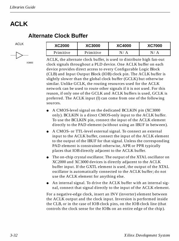
Libraries Guide
ACLK
Alternate Clock Buffer
ACLK, the alternate clock buffer, is used to distribute high fan-outclock signals throughout a PLD device. One ACLK buffer on eachdevice provides direct access to every Configurable Logic Block(CLB) and Input Output Block (IOB) clock pin. The ACLK buffer isslightly slower than the global clock buffer (GCLK) but otherwisesimilar. Unlike GCLK, the routing resources used for the ACLKnetwork can be used to route other signals if it is not used. For thisreason, if only one of the GCLK and ACLK buffers is used, GCLK ispreferred. The ACLK input (I) can come from one of the followingsources.
● A CMOS-level signal on the dedicated BCLKIN pin (XC3000only). BCLKIN is a direct CMOS-only input to the ACLK buffer.To use the BCLKIN pin, connect the input of the ACLK elementdirectly to the PAD element (without using an IBUF in between).
● A CMOS- or TTL-level external signal. To connect an externalinput to the ACLK buffer, connect the input of the ACLK elementto the output of the IBUF for that signal. Unless the correspondingPAD element is constrained otherwise, APR or PPR typicallyplaces that IOB directly adjacent to the ACLK buffer.
● The on-chip crystal oscillator. The output of the XTAL oscillator onXC2000 and XC3000 devices is directly adjacent to the ACLKbuffer input. If the GXTL element is used, the output of the XTALoscillator is automatically connected to the ACLK buffer; do notuse the ACLK element for anything else.
● An internal signal. To drive the ACLK buffer with an internal sig-nal, connect that signal directly to the input of the ACLK element.
For a negative-edge clock, insert an INV (inverter) element betweenthe ACLK output and the clock input. Inversion is performed insidethe CLB, or in the case of IOB clock pins, on the IOB clock line (thatcontrols the clock sense for the IOBs on an entire edge of the chip).
XC2000 XC3000 XC4000 XC7000
Primitive Primitive N/A N/A
ACLK
X3883
3-32 Xilinx Development System
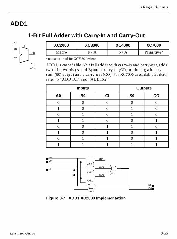
Design Elements
ADD1
1-Bit Full Adder with Carry-In and Carry-Out
* not supported for XC7336 designs
ADD1, a cascadable 1-bit full adder with carry-in and carry-out, addstwo 1-bit words (A and B) and a carry-in (CI), producing a binarysum (S0) output and a carry-out (CO). For XC7000 cascadable adders,refer to “ADD1X1” and “ADD1X2.”
Figure 3-7 ADD1 XC2000 Implementation
XC2000 XC3000 XC4000 XC7000
Macro N/A N/A Primitive*
Inputs Outputs
A0 B0 CI S0 CO
0 0 0 0 01 0 0 1 00 1 0 1 01 1 0 0 10 0 1 1 01 0 1 0 10 1 1 0 11 1 1 1 1
A0
S0
CO
CI
X4034
B0
AND2
AND2
AND2
XOR3
OR3B0CI
A0CI
AB0
CI
A0
S0
B0
CO
Libraries Guide 3-33

Libraries Guide
ADD1X1
1-Bit Cascadable Full Adder with Carry-Out for EPLD
* not supported for XC7336 designs
ADD1X1 is implemented using the EPLD arithmetic carry-logic chainfor high-speed ripple-carry addition. ADD1X1 is a low-order addercomponent, which can be used as a stand-alone or cascaded withhigh-order adders through its CO output. ADD1X2 adds two words(A0 and B0) and produces a sum output (ADD1X2) and carry-out(CO).
The CO output is passed into the EPLD carry chain, and therefore canonly be connected to the CI input of another EPLD-specific arithmeticcomponent. To generate a carry-out for general-purpose logic, use anadder (or cascaded adders) with one extra bit and tie the most-signif-icant A and B inputs to GND; the most-significant S output becomesthe carry-out. If a carry-in is required from general-purpose logic,extend the length of the adder by one additional bit and connect thecarry-in signal to both the least-significant A and B inputs (the least-significant S output is not used) to generate a carry into the carrychain for the second bit of the adder.
Refer to “ADD1” for truth table derivation.
XC2000 XC3000 XC4000 XC7000
N/A N/A N/A Primitive*
A0
S0
CO
X4224
B0
3-34 Xilinx Development System

Design Elements
ADD1X2
1-Bit Cascadable Full Adder with Carry-In andCarry-Out for EPLD
* not supported for XC7336 designs
ADD1X2 is implemented using the EPLD arithmetic carry-logic chainfor high-speed ripple-carry addition. ADD1X2 is a high-order addercomponent cascaded to lower-order adders through its CI input.ADD1X2 adds two words (A0 and B0) and a carry-in (CI), producinga sum output (S0) and carry-out (CO).
The CI input is taken from the EPLD carry chain, and therefore mustonly be connected to the CO output of another EPLD-specific arith-metic component. The CO output is passed into the EPLD carrychain, and therefore can only be connected to the CI input of anotherEPLD-specific arithmetic component. To generate a carry-out forgeneral-purpose logic, use an adder (or cascaded adders) with oneextra bit and tie the most-significant A and B inputs to GND; themost-significant S output becomes the carry-out.
Refer to “ADD1” for truth table derivation.
XC2000 XC3000 XC4000 XC7000
N/A N/A N/A Primitive*A0
S0
CO
CI
X4225
B0
Libraries Guide 3-35
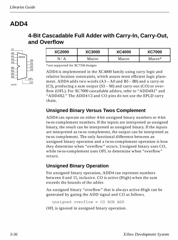
Libraries Guide
ADD4
4-Bit Cascadable Full Adder with Carry-In, Carry-Out,and Overflow
* not supported for XC7336 designs
ADD4 is implemented in the XC4000 family using carry logic andrelative location constraints, which assure most efficient logic place-ment. ADD4 adds two words (A3 – A0 and B3 – B0) and a carry-in(CI), producing a sum output (S3 – S0) and carry-out (CO) or over-flow (OFL). For XC7000 cascadable adders, refer to “ADD4X1” and“ADD4X2.” The ADD4 CI and CO pins do not use the EPLD carrychain.
Unsigned Binary Versus Twos ComplementADD4 can operate on either 4-bit unsigned binary numbers or 4-bittwos-complement numbers. If the inputs are interpreted as unsignedbinary, the result can be interpreted as unsigned binary. If the inputsare interpreted as twos complement, the output can be interpreted astwos complement. The only functional difference between anunsigned binary operation and a twos-complement operation is howthey determine when “overflow” occurs. Unsigned binary uses CO,while twos-complement uses OFL to determine when “overflow”occurs.
Unsigned Binary OperationFor unsigned binary operation, ADD4 can represent numbersbetween 0 and 15, inclusive. CO is active (High) when the sumexceeds the bounds of the adder.
An unsigned binary “overflow” that is always active-High can begenerated by gating the ADD signal and CO as follows.
unsigned overflow = CO XOR ADD
OFL is ignored in unsigned binary operation.
XC2000 XC3000 XC4000 XC7000
N/A Macro Macro Macro*A0
CI
ADD4
COX4376
A1A2A3
B0B1B2B3
S0S1S2S3
OFL
3-36 Xilinx Development System

Design Elements
Twos-Complement OperationFor twos-complement operation, ADD4 can represent numbersbetween -8 and +7, inclusive. OFL is active (High) when the sumexceeds the bounds of the adder.
CO is ignored in twos-complement operation.
XC4000 Topology
X3665
S 3
CO
OFL
S 2
S 1
S 0
B 3A 3
B 2A 2
B 1A 1
B 0A 0
CI
Libraries Guide 3-37
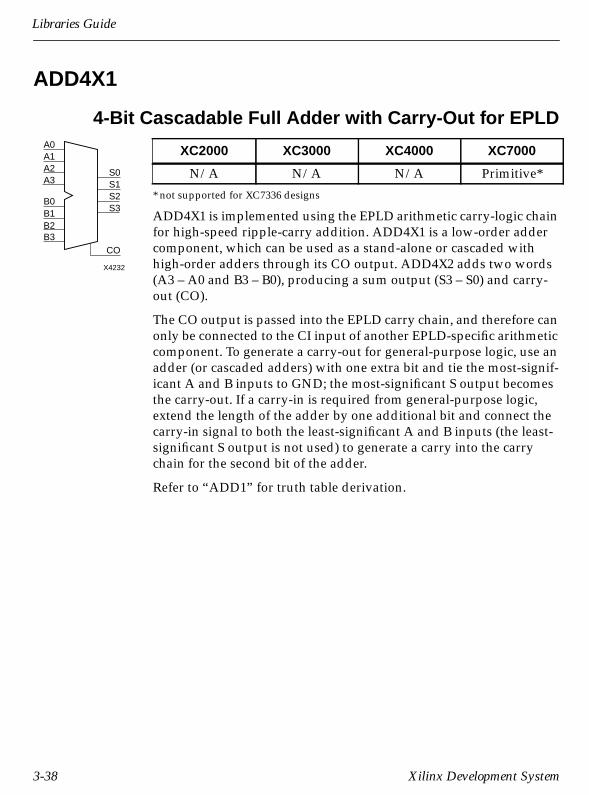
Libraries Guide
ADD4X1
4-Bit Cascadable Full Adder with Carry-Out for EPLD
* not supported for XC7336 designs
ADD4X1 is implemented using the EPLD arithmetic carry-logic chainfor high-speed ripple-carry addition. ADD4X1 is a low-order addercomponent, which can be used as a stand-alone or cascaded withhigh-order adders through its CO output. ADD4X2 adds two words(A3 – A0 and B3 – B0), producing a sum output (S3 – S0) and carry-out (CO).
The CO output is passed into the EPLD carry chain, and therefore canonly be connected to the CI input of another EPLD-specific arithmeticcomponent. To generate a carry-out for general-purpose logic, use anadder (or cascaded adders) with one extra bit and tie the most-signif-icant A and B inputs to GND; the most-significant S output becomesthe carry-out. If a carry-in is required from general-purpose logic,extend the length of the adder by one additional bit and connect thecarry-in signal to both the least-significant A and B inputs (the least-significant S output is not used) to generate a carry into the carrychain for the second bit of the adder.
Refer to “ADD1” for truth table derivation.
XC2000 XC3000 XC4000 XC7000
N/A N/A N/A Primitive*A2A1
A3
B0B1B2B3
S2S1S0
S3
CO
A0
X4232
3-38 Xilinx Development System
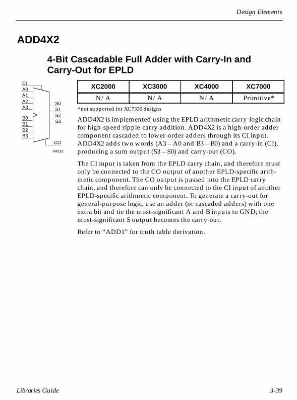
Design Elements
ADD4X2
4-Bit Cascadable Full Adder with Carry-In andCarry-Out for EPLD
* not supported for XC7336 designs
ADD4X2 is implemented using the EPLD arithmetic carry-logic chainfor high-speed ripple-carry addition. ADD4X2 is a high-order addercomponent cascaded to lower-order adders through its CI input.ADD4X2 adds two words (A3 – A0 and B3 – B0) and a carry-in (CI),producing a sum output (S3 – S0) and carry-out (CO).
The CI input is taken from the EPLD carry chain, and therefore mustonly be connected to the CO output of another EPLD-specific arith-metic component. The CO output is passed into the EPLD carrychain, and therefore can only be connected to the CI input of anotherEPLD-specific arithmetic component. To generate a carry-out forgeneral-purpose logic, use an adder (or cascaded adders) with oneextra bit and tie the most-significant A and B inputs to GND; themost-significant S output becomes the carry-out.
Refer to “ADD1” for truth table derivation.
XC2000 XC3000 XC4000 XC7000
N/A N/A N/A Primitive*A2A1
CI
A3
B0B1B2B3
S2S1S0
S3
CO
A0
X4233
Libraries Guide 3-39

Libraries Guide
ADD8
8-Bit Cascadable Full Adder with Carry-In, Carry-Out,and Overflow
* not supported for XC7336 designs
ADD8 is implemented in the XC4000 family using carry logic andrelative location constraints, which assure most efficient logic place-ment. ADD8 adds two words (A7 – A0 and B7 – B0) and a carry-in(CI), producing a sum output (S7 – S0) and carry-out (CO) or over-flow (OFL). For XC7000 cascadable adders, refer to “ADD8X1” and“ADD8X2.” The ADD8 CI and CO pins do not use the EPLD carrychain.
Unsigned Binary Versus Twos-ComplementADD8 can operate on either 8-bit unsigned binary numbers or 8-bittwos-complement numbers. If the inputs are interpreted as unsignedbinary, the result can be interpreted as unsigned binary. If the inputsare interpreted as twos complement, the output can be interpreted astwos complement. The only functional difference between anunsigned binary operation and a twos-complement operation is howthey determine when “overflow” occurs. Unsigned binary uses CO,while twos-complement uses OFL to determine when “overflow”occurs.
Unsigned Binary OperationFor unsigned binary operation, ADD8 can represent numbersbetween 0 and 255, inclusive. CO is active (High) when the sumexceeds the bounds of the adder.
An unsigned binary “overflow” that is always active-High can begenerated by gating the ADD signal and CO as follows.
unsigned overflow = CO XOR ADD
OFL is ignored in unsigned binary operation.
XC2000 XC3000 XC4000 XC7000
N/A Macro Macro Macro*A[7:0]
S[7:0]
CO
CI
X4377
B[7:0]
OFL
3-40 Xilinx Development System

Design Elements
Twos-Complement OperationFor twos-complement operation, ADD8 can represent numbersbetween -128 and +127, inclusive. OFL is active (High) when the sumexceeds the bounds of the adder.
CO is ignored in twos-complement operation.
XC4000 Topology
X3666
S 7
CO
OFL
S 6
S 5
S 4
B 7A 7
B 6A 6
B 5A 5
B 4A 4
CI
S 3
S 2
S 1
S 0
B 3A 3
B 2A 2
B 1A 1
B 0A 0
Libraries Guide 3-41

Libraries Guide
Figure 3-8 ADD8 XC3000 Implementation
OFL
OR3
XOR3
XOR3
OR3
XOR3
XOR3
OR3
OR3AND2
AND2
AND2
AND2
AND2
AND2
AND2
AND2
AND2 AND2
AND2
AND2
AND2
AND2
AND2
AND2
AND2
OR3
XOR3
OR3
XOR3
OR3
XOR3
AND2
AND2 AND2
AND2
AND2
OR3
XOR3
AND2
A7C6
AB6
AB5
AB4
AB3
AB2
AB1
A1C0
A2C1
A3C2
A4C3
A5C4
A6C5
B7C6
B6C5
B5C4
B4C3
B3C2
B2C1
B1C0
B0CI
AB0
C4
C5
C6C2
C1
CI
C0
CO
C3
A0CI
AB7
AND2XOR2
XNOR2
AND2
AABXSAAB
AXB
B7
B4
B5
B6
B[7:0]
B3
B0
B1
B2A2
A7
A6
A5
A4
A[7:0]
A3
A1
A0
S2
S3
S1
S0 S4
S5
S6
S7
S[7:0]
AND2
3-42 Xilinx Development System

Design Elements
Figure 3-9 ADD8 XC4000 Implementation
CO
OFL
OOR3
XOR2
OR3
OOR1
OOR2
I1I2I3I4
O
FMAPOR3
COR2
CO
COR1
COR3
C6A7
S6
S7B7
S[7:0]S7
C5
C4
C3
B4
B5
B6A6
A5
A4
S3
S4
S5
S6
S4
S5
C2
C1
B2
B3A3
A2S2
S2
S3
C0
B1A1
S1
S1
A0
ADD
B1
A1
B0
CY4
CIN
COUT
(F3)
(F1)
(F2)
(G4)
(G1)
CARRY MODE
S2XOR3
S1XOR3
C1
A0
ADD
B1A1B0
CY4
CIN
COUT
COUT0
(F3)
(F1)(F2)(G4)(G1)
CARRY MODE
C_INCY4_13ADDSUB-FG-CI
CY4_13
S0
XOR3
B0A0C_IN
S0
I1I2I3I4
O
FMAP
CI
B[7:0]
B0
B1
CY4_39FORCE-F1
A[7:0]
A0
A1
S0
C3
A0
ADD
B1
A1
B0
CIN
COUT
COUT0
(F3)
(F1)
(F2)
(G4)
(G1)
CARRY MODE
CY4_13
S3XOR3
S4XOR3
B2
B3
A3
A2
A0
ADD
B1
A1
B0
CY4
CIN
COUT
COUT0
(F1)
(F2)
(G4)
(G1)
CARRY MODE
ADDSUB-FG-CI
S6
XOR3S5
XOR3
B5
B4A5
A4
C5CY4_12ADDSUB-F-CI
S7XOR3
B6A6
A7
AND2
AND2
AND2
A0
ADD
B1
A1
B0
CY4
CIN
COUT
COUT0
(F3)
(F1)
(F2)
(G4)
(G1)
CARRY MODE
CY4_42EXAMINE-CI
C7
B7A7C7
AND2
B7
B7
AND2
AND2
A7
C7_M
C4
C2
C0
I1I2I3I4
O
FMAP
I1I2I3I4
O
FMAP
I1I2I3I4
O
FMAP
I1I2I3I4
O
FMAP
I1I2I3I4
O
FMAP
I1I2I3I4
O
FMAP
I1I2I3I4
O
FMAP
OFLA7C7
B7
I1I2I3I4
O
FMAP
X4333
C6
COUT0
COUT0
A0
ADD
B1
A1
B0
(F3)
(F1)
(F2)
(G4)
(G1) COUT
CY4
CY4
CARRY MODE
ADDSUB-FG-CI
(F3)
RLOC=R0C0.F
RLOC=R0C0.G
RLOC=R1C0.G
RLOC=R1C0.F
RLOC=R2C0.G
RLOC=R2C0.F
RLOC=R3C0.G
RLOC=R3C0.F
RLOC=R4C0.G
RLOC=R4C0.F
RLOC=R0C0
RLOC=R1C0
RLOC=R2C0
RLOC=R3C0
RLOC=R4C0
RLOC=R5C0
Libraries Guide 3-43

Libraries Guide
ADD8X1
8-Bit Loadable Cascadable Full Adder with Carry-Outfor EPLD
* not supported for XC7336 designs
ADD8X1 is implemented using the EPLD arithmetic carry-logic chainfor high-speed ripple-carry addition. ADD8X1 is a low-order addercomponent that can be used stand-alone or cascaded with high-orderadders through its CO output. ADD8X2 adds two words (A7 – A0and B7 – B0), producing a sum output (S7 – S0) and carry-out (CO).The CO output passes into the EPLD carry chain, and therefore canonly be connected to the CI input of another EPLD-specific arithmeticcomponent. To generate a carry-out for general-purpose logic, use anadder (or cascaded adders) with one extra bit and tie the most-signif-icant A and B inputs to GND; the most-significant S output becomesthe carry-out. If a carry-in is required from general-purpose logic,extend the length of the adder by one additional bit and connect thecarry-in signal to both the least-significant A and B inputs (the least-significant S output is not used). This procedure generates a carryinto the carry chain for the second bit of the adder.
Refer to “ADD1” for truth table derivation.
XC2000 XC3000 XC4000 XC7000
N/A N/A N/A Primitive*
A[7:0]
S[7:0]
CO
X4236
B[7:0]
3-44 Xilinx Development System

Design Elements
ADD8X2
8-Bit Cascadable Full Adder with Carry-In andCarry-Out for EPLD
* not supported for XC7336 designs
ADD8X2 is implemented using the EPLD arithmetic carry-logic chainfor high-speed ripple-carry addition. ADD8X2 is a high-order addercomponent cascaded to lower-order adders through its CI input.ADD8X2 adds two words (A7 – A0 and B7 – B0) and a carry-in (CI),producing a sum output (S7 – S0) and carry-out (CO).
The CI input is taken from the EPLD carry chain, and therefore mustonly be connected to the CO output of another EPLD-specific arith-metic component. The CO output is passed into the EPLD carrychain, and therefore can only be connected to the CI input of anotherEPLD-specific arithmetic component. To generate a carry-out forgeneral-purpose logic, use an adder (or cascaded adders) with oneextra bit and tie the most-significant A and B inputs to GND; themost-significant S output becomes the carry-out.
Refer to “ADD1” for truth table derivation.
XC2000 XC3000 XC4000 XC7000
N/A N/A N/A Primitive*A[7:0]
S[7:0]
CO
CI
X4237
B[7:0]
Libraries Guide 3-45

Libraries Guide
ADD16
16-Bit Cascadable Full Adder with Carry-In,Carry-Out, and Overflow
* not supported for XC7336 designs
ADD16 is implemented in the XC4000 family using carry logic andrelative location constraints, which assure most efficient logic place-ment. ADD16 adds two words (A15 – A0 and B15 – B0) and a carry-in(CI), producing a sum output (S15 – S0) and carry-out (CO) or over-flow (OFL). For XC7000 cascadable adders, refer to “ADD16X1” and“ADD16X2.” The ADD16 CI and CO pins do not use the EPLD carrychain.
Unsigned Binary Versus Twos-ComplementADD16 can operate on either 16-bit unsigned binary numbers or16-bit twos-complement numbers. If the inputs are interpreted asunsigned binary, the result can be interpreted as unsigned binary. Ifthe inputs are interpreted as twos complement, the output can beinterpreted as twos complement. The only functional differencebetween an unsigned binary operation and a twos-complement oper-ation is how they determine when “overflow” occurs. Unsignedbinary uses CO, while twos-complement uses OFL to determinewhen “overflow” occurs.
Unsigned Binary OperationFor unsigned binary operation, ADD16 can represent numbersbetween 0 and 65535, inclusive. CO is active (High) when the sumexceeds the bounds of the adder.
An unsigned binary “overflow” that is always active-High can begenerated by gating the ADD signal and CO as follows.
unsigned overflow = CO XOR ADD
OFL is ignored in unsigned binary operation.
XC2000 XC3000 XC4000 XC7000
N/A Macro Macro Macro*
A[15:0]
S[15:0]
CO
CI
X4378
B[15:0]
OFL
3-46 Xilinx Development System

Design Elements
Twos-Complement OperationFor twos-complement operation, ADD16 can represent numbersbetween -32768 and +32767, inclusive. OFL is active (High) when thesum exceeds the bounds of the adder.
CO is ignored in twos-complement operation.
XC4000 Topology
X3667
S 15
CO
OFL
S 14
S 13
S 12
B 15A 15
CI
S 11
S 10
S 9
S 8
B 9A 9
B 8A 8
S 7
S 6
S 5
S 4
B 7A 7
B 6A 6
B 5A 5
B 4A 4
S 3
S 2
S 1
S 0
B 3A 3
B 2A 2
B 1A 1
B 0A 0
B 14A 14
B 13A 13
B 12A 12
B 11A 11
B 10A 10
Libraries Guide 3-47

Libraries Guide
Figure 3-10 ADD16 XC7000 Implementation
B[15:8]
B15
B[15:0]
B[7:0]
A[15:8]
A15
A[15:0]
A[7:0]
S15
S[15:0]
S[7:0]
S[15:8]
OFL_OUT
OR2
OFL_NEG
AND3B1
OFL_POS
AND3B2
CO15
ADD1X2
S0B0
A0
CO
CI
CI0
CO
ADD1X1
S0B0
A0
OFL
CO
S7_0
ADD8X2
CO
A[7:0]
B[7:0]S[7:0]
CI
S15_8
ADD8X2
CO
A[7:0]
B[7:0]S[7:0]
CI
CI
GND
3-48 Xilinx Development System

Design Elements
ADD16X1
16-Bit Cascadable Full Adder with Carry-Out forEPLD
* not supported for XC7336 designs
ADD16X1 is implemented using the EPLD arithmetic carry-logicchain for high-speed ripple-carry addition. ADD16X1 is a low-orderadder component, which can be used as a stand-alone or cascadedwith high-order adders through its CO output. ADD16X2 adds twowords (A15 – A0 and B15 – B0), producing a sum output (S15 – S0)and carry-out (CO).
The CO output is passed into the EPLD carry chain, and therefore canonly be connected to the CI input of another EPLD-specific arithmeticcomponent. To generate a carry-out for general-purpose logic, use anadder (or cascaded adders) with one extra bit and tie the most-signif-icant A and B inputs to GND; the most-significant S output becomesthe carry-out. If a carry-in is required from general-purpose logic,extend the length of the adder by one additional bit and connect thecarry-in signal to both the least-significant A and B inputs (the least-significant S output is not used) to generate a carry into the carrychain for the second bit of the adder.
Refer to “ADD1” for truth table derivation.
XC2000 XC3000 XC4000 XC7000
N/A N/A N/A Macro*
A[15:0]
S[15:0]
CO
X4317
B[15:0]
Libraries Guide 3-49
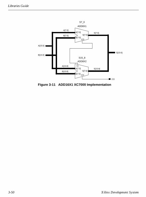
Libraries Guide
Figure 3-11 ADD16X1 XC7000 Implementation
S[15:0]
S[15:8]
S[7:0]
B[15:0]
B[7:0]
B[15:8]
A[15:0]
A[15:8]
A[7:0]
CO
S15_8
ADD8X2
CO
A[7:0]
B[7:0]
S[7:0]
CI
S7_0
ADD8X1
S[7:0]B[7:0]
A[7:0]
CO
3-50 Xilinx Development System

Design Elements
ADD16X2
16-Bit Cascadable Full Adder with Carry-In andCarry-Out for EPLD
* not supported for XC7336 designs
ADD16X2 is implemented using the EPLD arithmetic carry-logicchain for high-speed ripple-carry addition. ADD16X2 is a high-orderadder component cascaded to lower-order adders through its CIinput. ADD16X2 adds two words (A15 – A0 and B15 – B0) and acarry-in (CI), producing a sum output (S15 – S0) and carry-out (CO).
The CI input is taken from the EPLD carry chain, and therefore mustonly be connected to the CO output of another EPLD-specific arith-metic component. The CO output is passed into the EPLD carrychain, and therefore can only be connected to the CI input of anotherEPLD-specific arithmetic component. To generate a carry-out forgeneral-purpose logic, use an adder (or cascaded adders) with oneextra bit and tie the most-significant A and B inputs to GND; themost-significant S output becomes the carry-out. Refer to “ADD1” fortruth table derivation.
Figure 3-12 ADD16X2 XC7000 Implementation
XC2000 XC3000 XC4000 XC7000
N/A N/A N/A Macro*A[15:0]
S[15:0]
CO
CI
X4318
B[15:0]
CI
S15_8
ADD8X2
CO
A[7:0]
B[7:0]S[7:0]
CI
CO
A[7:0]
A[15:8]
A[15:0]
B[15:8]
B[7:0]
B[15:0]
S[7:0]
S[15:8]
S[15:0]
S7_0
ADD8X2
CO
A[7:0]
B[7:0]S[7:0]
CI
Libraries Guide 3-51

Libraries Guide
ADSU1
1-Bit Cascadable Adder/Subtracter with Carry-In andCarry-Out
* not supported for XC7336 designs
When the ADD input is High, two 1-bit words (A0 and B0) are addedwith a carry-in (CI), producing a 1-bit output (S0) and a carry-out(CO). When the ADD input is Low, B0 is subtracted from A0,producing a result (S0) and borrow (CO). In add mode, CO representsa carry-out, and CO and CI are active-High. In subtract mode, COrepresents a borrow, and CO and CI are active-Low. Refer to“ADSU1X1” and “ADSU1X2” for cascadable EPLD symbols.
Add Function, ADD=1
XC2000 XC3000 XC4000 XC7000
Macro N/A N/A Primitive*
Inputs Outputs
A0 B0 CI S0 CO
0 0 0 0 00 1 0 1 01 0 0 1 01 1 0 0 10 0 1 1 00 1 1 0 11 0 1 0 11 1 1 1 1
A0
S0
ADD CO
CI
X4035
B0
3-52 Xilinx Development System

Design Elements
Subtract Function, ADD=0
Figure 3-13 ADSU1 XC2000 Implementation
Inputs Outputs
A0 B0 CI S0 CO
0 0 0 1 00 1 0 0 01 0 0 0 11 1 0 1 00 0 1 0 10 1 1 1 01 0 1 1 11 1 1 0 1
ADD
ADD_C0
SUB_C0A1CI
A3_0
A2_0
A1_0
A0_0
CO
B0A0
CI
S0
A2CICO
D0D1
O
S0
M2_1AND2B1
OR2B1
OR2
AND2
AND2 OR2
AND2OR2
XNOR4
Libraries Guide 3-53
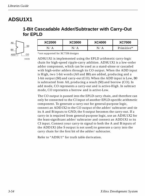
Libraries Guide
ADSU1X1
1-Bit Cascadable Adder/Subtracter with Carry-Outfor EPLD
* not supported for XC7336 designs
ADSU1X1 is implemented using the EPLD arithmetic carry-logicchain for high-speed ripple-carry addition. ADSU1X1 is a low-orderadder component, which can be used as a stand-alone or cascadedwith high-order adders through its CO output. When the ADD inputis High, two 1-bit words (A0 and B0) are added, producing and a1-bit output (S0) and carry-out (CO). When the ADD input is Low, B0is subtracted from A0, producing a result (S0) and borrow (CO). Inadd mode, CO represents a carry-out and is active-High. In subtractmode, CO represents a borrow and is active-Low.
The CO output is passed into the EPLD carry chain, and therefore canonly be connected to the CI input of another EPLD-specific arithmeticcomponent. To generate a carry-out for general-purpose logic,connect an ADD1X2 to the CO output of the adder/subtracter and tieits A and B inputs to GND; the S output becomes the carry-out. If acarry-in is required from general-purpose logic, use an ADSU1X2 forthe least-significant adder/subtracter and connect an ADD1X1 to itsCI input. Connect your carry-in signal to both the A and B inputs ofthe ADD1X1 (the S output is not used) to generate a carry into thecarry chain for the first bit of the adder/subtracter.
Refer to “ADSU1” for truth table derivation.
XC2000 XC3000 XC4000 XC7000
N/A N/A N/A Primitive*
A0
S0
ADD CO
X4226
B0
3-54 Xilinx Development System

Design Elements
ADSU1X2
1-Bit Cascadable Adder/Subtracter with Carry-In andCarry-Out for EPLD
* not supported for XC7336 designs
ADSU1X2 is implemented using the EPLD arithmetic carry-logicchain for high-speed ripple-carry addition. ADSU1X2 is a high-orderadder component cascaded to lower-order adders through its CIinput. When the ADD input is High, two 1-bit words (A0 and B0) areadded with a carry-in (CI), producing a 1-bit output (S0) and carry-out (CO). When the ADD input is Low, B0 is subtracted from A0,producing a result (S0) and borrow (CO). In add mode, CO repre-sents a carry-out, and CO and CI are active-High. In subtract mode,CO represents a borrow, and CO and CI are active-Low.
The CI input is taken from the EPLD carry chain, and therefore mustonly be connected to the CO output of another EPLD-specific arith-metic component. The CO output is passed into the EPLD carrychain, and therefore can only be connected to the CI input of anotherEPLD-specific arithmetic component. To generate a carry-out signalfor general-purpose logic, connect an ADD1X2 to the CO output ofthe adder/subtracter and tie its A and B inputs to GND; the S outputbecomes the carry-out.
Refer to “ADSU1” for truth table derivation.
XC2000 XC3000 XC4000 XC7000
N/A N/A N/A Primitive*A0
S0
ADD CO
CI
X4227
B0
Libraries Guide 3-55

Libraries Guide
ADSU4
4-Bit Cascadable Adder/Subtracter with Carry-In,Carry-Out, and Overflow
* not supported for XC7336 designs
ADSU4 is implemented in the XC4000 family using carry logic andrelative location constraints, which assure most efficient logic place-ment. When the ADD input is High, two 4-bit words (A3 – A0 andB3 – B0) are added with a carry-in (CI), producing a 4-bit sum(S3 – S0) and carry-out (CO) or overflow (OFL). When the ADD inputis Low, B3 – B0 is subtracted from A3 – A0, producing a 4-bit differ-ence (S3 – S0) and CO or OFL. In add mode, CO and CI are active-High. In subtract mode, CO and CI are active-Low. For cascadableEPLD symbols, refer to “ADSU4X1” and “ADSU4X2.” ADSU4 CI andCO pins do not use the EPLD carry chain.
Unsigned Binary Versus Twos-ComplementADSU4 can operate on either 4-bit unsigned binary numbers or 4-bittwos-complement numbers. If the inputs are interpreted as unsignedbinary, the result can be interpreted as unsigned binary. If the inputsare interpreted as twos complement, the output can be interpreted astwos complement. The only functional difference between anunsigned binary operation and a twos-complement operation is howthey determine when “overflow” occurs. Unsigned binary uses CO,while twos-complement uses OFL to determine when “overflow”occurs.
With adder/subtracters, either unsigned binary or twos-complementoperations cause an overflow. If the result crosses the overflowboundary, an overflow is generated. Similarly, when the result crossesthe carry-out boundary, a carry-out is generated. The following figureshows the ADSU carry-out and overflow boundaries.
XC2000 XC3000 XC4000 XC7000
N/A Macro Macro Macro*A2A1
CI
A3
B0B1B2B3ADD
S2S1S0
S3
CO
A0
X4379
OFL
3-56 Xilinx Development System

Design Elements
Figure 3-14 ADSU Carry-Out and Overflow Boundaries
Unsigned Binary OperationFor unsigned binary operation, ADSU4 can represent numbersbetween 0 and 15, inclusive. In add mode, CO is active (High) whenthe sum exceeds the bounds of the adder/subtracter. In subtractmode, CO is an active-Low borrow-out and goes Low when thedifference exceeds the bounds.
An unsigned binary “overflow” that is always active-High can begenerated by gating the ADD signal and CO as follows.
unsigned overflow = CO XOR ADD
OFL is ignored in unsigned binary operation.
Twos-Complement OperationFor twos-complement operation, ADSU4 can represent numbersbetween -8 and +7, inclusive. If an addition or subtraction operationresult exceeds this range, the OFL output goes High.
CO is ignored in twos-complement operation.
TWO
SC
OM
PL
EM
EN
TO
RS
IGNED
TW
OSC
OM
PL
EM
EN
TO
RS
IGN
ED
UNS
IGN
ED
BIN
AR
Y
UN
SIG
NE
DB
INA
RY
X4720
255
-127 127
127128
0
0-1
Overflow
Carry-Out
Libraries Guide 3-57

Libraries Guide
XC4000 Topology
X3668
CO
OFL
CI
S 3
S 2
S 1
S 0
B 3A 3
B 2A 2
B 1A 1
B 0A 0
3-58 Xilinx Development System
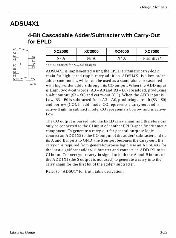
Design Elements
ADSU4X1
4-Bit Cascadable Adder/Subtracter with Carry-Outfor EPLD
* not supported for XC7336 designs
ADSU4X1 is implemented using the EPLD arithmetic carry-logicchain for high-speed ripple-carry addition. ADSU4X1 is a low-orderadder component, which can be used as a stand-alone or cascadedwith high-order adders through its CO output. When the ADD inputis High, two 4-bit words (A3 – A0 and B3 – B0) are added, producinga 4-bit output (S3 – S0) and carry-out (CO). When the ADD input isLow, B3 – B0 is subtracted from A3 – A0, producing a result (S3 – S0)and borrow (CO). In add mode, CO represents a carry-out and isactive-High. In subtract mode, CO represents a borrow and is active-Low.
The CO output is passed into the EPLD carry chain, and therefore canonly be connected to the CI input of another EPLD-specific arithmeticcomponent. To generate a carry-out for general-purpose logic,connect an ADD1X2 to the CO output of the adder/subtracter and tieits A and B inputs to GND; the S output becomes the carry-out. If acarry-in is required from general-purpose logic, use an ADSU4X2 forthe least-significant adder/subtracter and connect an ADD1X1 to itsCI input. Connect your carry-in signal to both the A and B inputs ofthe ADD1X1 (the S output is not used) to generate a carry into thecarry chain for the first bit of the adder/subtracter.
Refer to “ADSU1” for truth table derivation.
XC2000 XC3000 XC4000 XC7000
N/A N/A N/A Primitive*A2A1
A3
B0B1B2B3ADD
S2S1S0
S3
CO
A0
X4234
Libraries Guide 3-59

Libraries Guide
ADSU4X2
4-Bit Cascadable Adder/Subtracter with Carry-In andCarry-Out for EPLD
* not supported for XC7336 designs
ADSU4X2 is implemented using the EPLD arithmetic carry-logicchain for high-speed ripple-carry addition. ADSU4X2 is a high-orderadder component cascaded to lower-order adders through its CIinput. When the ADD input is High, two 4-bit words (A3 – A0 andB3 – B0) are added with a carry-in (CI), producing a 4-bit output(S3 – S0) and carry-out (CO). When the ADD input is Low, B3 – B0 issubtracted from A3 – A0, producing a result (S3 – S0) and borrow(CO). In add mode, CO represents a carry-out, and CO and CI areactive-High. In subtract mode, CO represents a borrow, and CO andCI are active-Low.
The CI input is taken from the EPLD carry chain, and therefore mustonly be connected to the CO output of another EPLD-specific arith-metic component. The CO output is passed into the EPLD carrychain, and therefore can only be connected to the CI input of anotherEPLD-specific arithmetic component. To generate a carry-out signalfor general-purpose logic, connect an ADD1X2 to the CO output ofthe adder/subtracter and tie its A and B inputs to GND; the S outputbecomes the carry-out.
Refer to “ADSU1” for truth table derivation.
XC2000 XC3000 XC4000 XC7000
N/A N/A N/A Primitive*A2A1
CI
A3
B0B1B2B3ADD
S2S1S0
S3
CO
A0
X4235
3-60 Xilinx Development System

Design Elements
ADSU8
8-Bit Cascadable Adder/Subtracter with Carry-In,Carry-Out, and Overflow
* not supported for XC7336 designs
ADSU8 is implemented in the XC4000 family using carry logic andrelative location constraints, which assure most efficient logic place-ment. When the ADD input is High, two 8-bit words (A7 – A0 andB7 – B0) are added with a carry-in (CI), producing an 8-bit sum(S7 – S0) and carry-out (CO) or overflow (OFL). When the ADD inputis Low, B7 – B0 is subtracted from A7 – A0, producing an 8-bit differ-ence (S7 – S0) and CO or OFL. In add mode, CO and CI are active-High. In subtract mode, CO and CI are active-Low. OFL is active-High in add and subtract modes. For cascadable EPLD symbols, referto “ADSU8X1” and “ADSU8X2.” ADSU8 CI and CO pins do not usethe EPLD carry chain.
Unsigned Binary Versus Twos-ComplementADSU8 can operate on either 8-bit unsigned binary numbers or 8-bittwos-complement numbers. If the inputs are interpreted as unsignedbinary, the result can be interpreted as unsigned binary. If the inputsare interpreted as twos complement, the output can be interpreted astwos complement. The only functional difference between anunsigned binary operation and a twos-complement operation is howthey determine when “overflow” occurs. Unsigned binary uses CO,while twos-complement uses OFL to determine when “overflow”occurs.
With adder/subtracters, either unsigned binary or twos-complementoperations cause an overflow. If the result crosses the overflowboundary, an overflow is generated. Similarly, when the resultcrosses the carry-out boundary, a carry-out is generated. Thefollowing figure shows the ADSU carry-out and overflow bound-aries.
XC2000 XC3000 XC4000 XC7000
N/A Macro Macro Macro*
A[7:0]
S[7:0]
ADDCO
CI
X4380
B[7:0]
OFL
Libraries Guide 3-61

Libraries Guide
Figure 3-15 ADSU Carry-Out and Overflow Boundaries
Unsigned Binary OperationFor unsigned binary operation, ADSU8 can represent numbersbetween 0 and 255, inclusive. In add mode, CO is active (High) whenthe sum exceeds the bounds of the adder/subtracter. In subtractmode, CO is an active-Low borrow-out and goes Low when thedifference exceeds the bounds.
An unsigned binary “overflow” that is always active-High can begenerated by gating the ADD signal and CO as follows.
unsigned overflow = CO XOR ADD
OFL is ignored in unsigned binary operation.
Twos-Complement OperationFor twos-complement operation, ADSU8 can represent numbersbetween -128 and +127, inclusive. If an addition or subtraction opera-tion result exceeds this range, the OFL output goes High.
CO is ignored in twos complement operation.
TWO
SC
OM
PL
EM
EN
TO
RS
IGNED
TW
OSC
OM
PL
EM
EN
TO
RS
IGN
ED
UNS
IGN
ED
BIN
AR
Y
UN
SIG
NE
DB
INA
RY
X4720
255
-127 127
127128
0
0-1
Overflow
Carry-Out
3-62 Xilinx Development System

Design Elements
XC4000 Topology
X3669
S 7
CO
OFL
S 6
S 5
S 4
B 7A 7
B 6A 6
B 5A 5
B 4A 4
CI
S 3
S 2
S 1
S 0
B 3A 3
B 2A 2
B 1A 1
B 0A 0
Libraries Guide 3-63

Libraries Guide
Figure 3-16 ADSU8 XC3000 Implementation
S7
S0
S1
S2
S3
S[7:0]
S4
S5
S6
ADD
A7
A[7:0]
A1
A0
A2
A3
A5
A4
A6
ADD_COA2C6
A3_7 OR2
C6
D0D1 O
S0
M2_1
C5
D0D1 O
S0
M2_1
C4
D0D1 O
S0
M2_1AND2B1
C0
D0D1 O
S0
M2_1
OR2OR2B1
AND2
OR2 AND2 OR2
AND2
XNOR4
C3
D0D1 O
S0
M2_1
OR2B1
AND2
AND2 OR2
AND2 OR2
C1
D0D1 O
S0
M2_1
XNOR4
AND2B1
XNOR4
OR2AND2
OR2AND2
XNOR4
OR2AND2
OR2AND2OR2
OR2B1
AND2B1
C2
D0D1 O
S0
M2_1
AND2
OR2
OR2B1
AND2B1
OR2
AND2 AND2
OR2
AND2B1
OR2B1
OR2
AND2
AND2B1
OR2B1
OR2 AND2 OR2
AND2 OR2
XNOR4
AND2 OR2
AND2 OR2
XNOR4
AND2B1
XNOR4
OR2AND2
AND2
AND2
OR2B1 CO
D0D1
O
S0
M2_1
XNOR4
AND2
OR2AND2OR2
AND2
OR2B1 OR2
AND2B1
A1C6
A0_7
A3_6
A2_6
C5
A1_6
A0_6
A2_5
A1_5
A0_5
A2_7
A1_7
A3_5
A3_4
A2_4
A1_4
A0_4
A1_3
A0_3
A3_3
A2_3
A3_2
A2_2
A1_2
A3_1
A2_1
A1_1
A0_1
A3_0
A1CI
A2_0
A0_0
A1_0
A2C5
A1C5
A2C4
A2C3
A2C2
A1C2
A2C1
A1C1
A1C0
SUB_CO
ADD_C6
SUB_C6
A1C4
ADD_C5
SUB_C5
ADD_C4
C4SUB_C4
C3
C2
ADD_C3
CI
SUB_C0
ADD_C0A2CI
SUB_C3
SUB_C2
ADD_C2
A2C0
SUB_C1
ADD_C1
C0
C1
C6
A1C3
A0_2
CO
B7
B0
B1
B2
B3
B[7:0]
B6
B5
B4
XNOR2
AND2XOR2
XNOR2
AND2
AABXSAAB
B_M
OFL
AXB
3-64 Xilinx Development System

Design Elements
Figure 3-17 ADSU8 XC4000 Implementation
CO
OFL
OFOR3
XOR2
OR3
OFOR1
OFOR2
OR3
OFL
COR2
COR1
COR3
C6A7
S6
S7B7ADD
A7
ADD
C7_M
B7
S[7:0]S7
ADD
ADD
ADD
C5
C4
C3
B4
B5
B6A6
A5
A4
S3
S4
S5
S6
S4
S5
ADD
ADD
C2
C1
B2
B3A3
A2S2
S2
S3
ADD
C0
B1A1
S1
S1
A0
ADD
B1
A1
B0
CY4
CIN
COUT
(F3)
(F1)
(F2)
(G4)
(G1)
CARRY MODE
S2XNOR4
S1XNOR4
C1
A0
ADD
B1A1B0
CY4
CIN
COUT
COUT0
(F3)
(F1)(F2)(G4)(G1)
CARRY MODE
C_INCY4_13ADDSUB-FG-CI
CY4_13
S0
XNOR4
ADDB0A0C_IN
S0
I1I2I3I4
O
FMAP
CI
B[7:0]
B0
B1
ADD
CY4_39FORCE-F1
A[7:0]
A0
A1
S0
C3
A0
ADD
B1
A1
B0
CIN
COUT
COUT0
(F3)
(F1)
(F2)
(G4)
(G1)
CARRY MODE
CY4_13
S3XNOR4
S4XNOR4
B2
B3
A3
A2
A0
ADD
B1
A1
B0
CY4
CIN
COUT
COUT0
(F1)
(F2)
(G4)
(G1)
CARRY MODE
ADDSUB-FG-CI
S6
XNOR4S5
XNOR4
B5
B4A5
A4
C5
CY4_12ADDSUB-F-CI
S7XNOR4
B6A6
A7
AND2
B7_M2XNOR2
AND2
AND2A0
ADD
B1
A1
B0
CY4
CIN
COUT
COUT0
(F3)
(F1)
(F2)
(G4)
(G1)
CARRY MODE
CY4_42EXAMINE-CI
C7
AND2XNOR2
B7
B7
B7
B7_M1
AND2
AND2
A7
C7_M
C4
C2
C0
I1I2I3I4
O
FMAP
I1I2I3I4
O
FMAP
I1I2I3I4
O
FMAP
I1I2I3I4
O
FMAP
I1I2I3I4
O
FMAP
I1I2I3I4
O
FMAP
I1I2I3I4
O
FMAP
I1I2I3I4
O
FMAP
X4280
C6
COUT0
COUT0
A0
ADD
B1
A1
B0
(F3)
(F1)
(F2)
(G4)
(G1) COUT
CY4
CY4
CARRY MODE
ADDSUB-FG-CI
I1I2I3I4
O
FMAP
CO
ADDB7A7C7_M
RLOC=R0C0.G
RLOC=R0C0.F
RLOC=R1C0.G
RLOC=R1C0.F
RLOC=R2C0.G
RLOC=R2C0.F
RLOC=R3C0.G
RLOC=R3C0.F
RLOC=R4C0.G
RLOC=R4C0.F
RLOC=R0C0
Libraries Guide 3-65
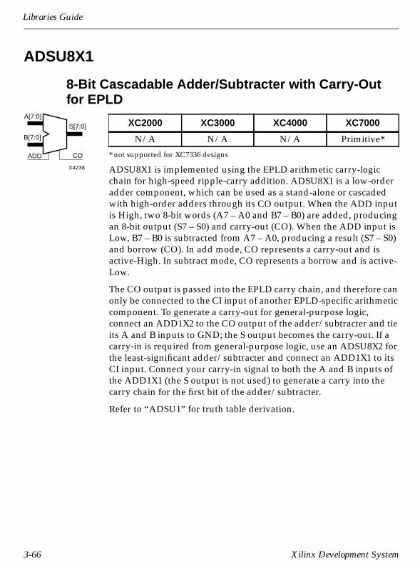
Libraries Guide
ADSU8X1
8-Bit Cascadable Adder/Subtracter with Carry-Outfor EPLD
* not supported for XC7336 designs
ADSU8X1 is implemented using the EPLD arithmetic carry-logicchain for high-speed ripple-carry addition. ADSU8X1 is a low-orderadder component, which can be used as a stand-alone or cascadedwith high-order adders through its CO output. When the ADD inputis High, two 8-bit words (A7 – A0 and B7 – B0) are added, producingan 8-bit output (S7 – S0) and carry-out (CO). When the ADD input isLow, B7 – B0 is subtracted from A7 – A0, producing a result (S7 – S0)and borrow (CO). In add mode, CO represents a carry-out and isactive-High. In subtract mode, CO represents a borrow and is active-Low.
The CO output is passed into the EPLD carry chain, and therefore canonly be connected to the CI input of another EPLD-specific arithmeticcomponent. To generate a carry-out for general-purpose logic,connect an ADD1X2 to the CO output of the adder/subtracter and tieits A and B inputs to GND; the S output becomes the carry-out. If acarry-in is required from general-purpose logic, use an ADSU8X2 forthe least-significant adder/subtracter and connect an ADD1X1 to itsCI input. Connect your carry-in signal to both the A and B inputs ofthe ADD1X1 (the S output is not used) to generate a carry into thecarry chain for the first bit of the adder/subtracter.
Refer to “ADSU1” for truth table derivation.
XC2000 XC3000 XC4000 XC7000
N/A N/A N/A Primitive*
A[7:0]
S[7:0]
ADD CO
X4238
B[7:0]
3-66 Xilinx Development System

Design Elements
ADSU8X2
8-Bit Cascadable Adder/Subtracter with Carry-In andCarry-Out for EPLD
* not supported for XC7336 designs
ADSU8X2 is implemented using the EPLD arithmetic carry-logicchain for high-speed ripple-carry addition. ADSU8X2 is a high-orderadder component cascaded to lower-order adders through its CIinput. When the ADD input is High, two 8-bit words (A7 – A0 andB7 – B0) are added with a carry-in (CI), producing an 8-bit output(S7 – S0) and carry-out (CO). When the ADD input is Low, B7 – B0 issubtracted from A7 – A0, producing a result (S7 – S0) and borrow(CO). In add mode, CO represents a carry-out, and CO and CI areactive-High. In subtract mode, CO represents a borrow, and CO andCI are active-Low.
The CI input is taken from the EPLD carry chain, and therefore mustonly be connected to the CO output of another EPLD-specific arith-metic component. The CO output is passed into the EPLD carrychain, and therefore can only be connected to the CI input of anotherEPLD-specific arithmetic component. To generate a carry-out signalfor general-purpose logic, connect an ADD1X2 to the CO output ofthe adder/subtracter and tie its A and B inputs to GND; the S outputbecomes the carry-out.
Refer to “ADSU1” for truth table derivation.
XC2000 XC3000 XC4000 XC7000
N/A N/A N/A Primitive*A[7:0]
S[7:0]
ADD CO
CI
X4239
B[7:0]
Libraries Guide 3-67
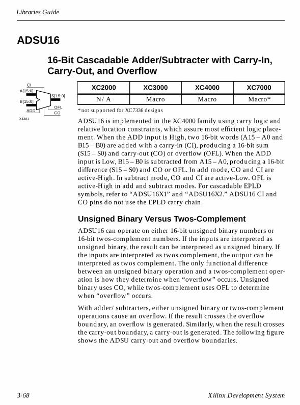
Libraries Guide
ADSU16
16-Bit Cascadable Adder/Subtracter with Carry-In,Carry-Out, and Overflow
* not supported for XC7336 designs
ADSU16 is implemented in the XC4000 family using carry logic andrelative location constraints, which assure most efficient logic place-ment. When the ADD input is High, two 16-bit words (A15 – A0 andB15 – B0) are added with a carry-in (CI), producing a 16-bit sum(S15 – S0) and carry-out (CO) or overflow (OFL). When the ADDinput is Low, B15 – B0 is subtracted from A15 – A0, producing a 16-bitdifference (S15 – S0) and CO or OFL. In add mode, CO and CI areactive-High. In subtract mode, CO and CI are active-Low. OFL isactive-High in add and subtract modes. For cascadable EPLDsymbols, refer to “ADSU16X1” and “ADSU16X2.” ADSU16 CI andCO pins do not use the EPLD carry chain.
Unsigned Binary Versus Twos-ComplementADSU16 can operate on either 16-bit unsigned binary numbers or16-bit twos-complement numbers. If the inputs are interpreted asunsigned binary, the result can be interpreted as unsigned binary. Ifthe inputs are interpreted as twos complement, the output can beinterpreted as twos complement. The only functional differencebetween an unsigned binary operation and a twos-complement oper-ation is how they determine when “overflow” occurs. Unsignedbinary uses CO, while twos-complement uses OFL to determinewhen “overflow” occurs.
With adder/subtracters, either unsigned binary or twos-complementoperations cause an overflow. If the result crosses the overflowboundary, an overflow is generated. Similarly, when the result crossesthe carry-out boundary, a carry-out is generated. The following figureshows the ADSU carry-out and overflow boundaries.
XC2000 XC3000 XC4000 XC7000
N/A Macro Macro Macro*A[15:0]
B[15:0]S[15:0]
ADDOFL
CI
X4381
CO
3-68 Xilinx Development System
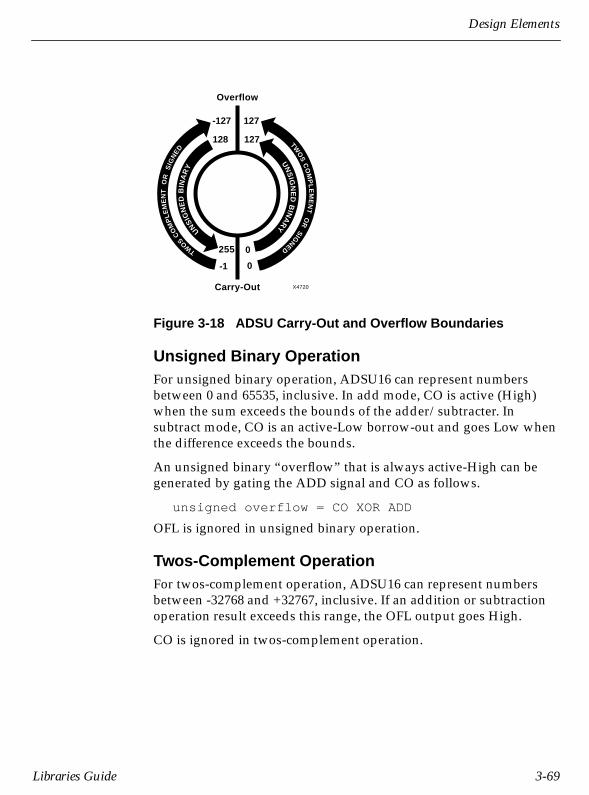
Design Elements
Figure 3-18 ADSU Carry-Out and Overflow Boundaries
Unsigned Binary OperationFor unsigned binary operation, ADSU16 can represent numbersbetween 0 and 65535, inclusive. In add mode, CO is active (High)when the sum exceeds the bounds of the adder/subtracter. Insubtract mode, CO is an active-Low borrow-out and goes Low whenthe difference exceeds the bounds.
An unsigned binary “overflow” that is always active-High can begenerated by gating the ADD signal and CO as follows.
unsigned overflow = CO XOR ADD
OFL is ignored in unsigned binary operation.
Twos-Complement OperationFor twos-complement operation, ADSU16 can represent numbersbetween -32768 and +32767, inclusive. If an addition or subtractionoperation result exceeds this range, the OFL output goes High.
CO is ignored in twos-complement operation.
TWO
SC
OM
PL
EM
EN
TO
RS
IGNED
TW
OSC
OM
PL
EM
EN
TO
RS
IGN
ED
UNS
IGN
ED
BIN
AR
Y
UN
SIG
NE
DB
INA
RY
X4720
255
-127 127
127128
0
0-1
Overflow
Carry-Out
Libraries Guide 3-69

Libraries Guide
XC4000 Topology
X3670
S 15
CO
OFL
S 14
S 13
S 12
B 15A 15
CI
S 11
S 10
S 9
S 8
B 9A 9
B 8A 8
S 7
S 6
S 5
S 4
B 7A 7
B 6A 6
B 5A 5
B 4A 4
S 3
S 2
S 1
S 0
B 3A 3
B 2A 2
B 1A 1
B 0A 0
B 14A 14
B 13A 13
B 12A 12
B 11A 11
B 10A 10
3-70 Xilinx Development System

Design Elements
Figure 3-19 ADSU16 XC7000 Implementation
ADD
CO
ADD1X1
S0B0
A0
OFL_OUT
OFL_NEG_SUB
OFL_POS_SUB
OFL_NEG_ADD
OFL_POS_ADD
OFL
B[15:0]
B[15:8]
B[7:0]
ADD1X2
S0
B0
A0
CO
CI
CO15
CO
CI
S15_8
S7_0
CI0
A[7:0]
A[15:0]
A[15:8]
ADSU8X2
ADD
CI
S[7:0]B[7:0]
A[7:0]
CO
S[7:0]
ADSU8X2
ADD
CI
S[7:0]B[7:0]
A[7:0]
COS[15:8]
GND
AND4B2
AND4B1
AND4B2
AND4B3
OR4
S[15:0]
B15A15
S15
Libraries Guide 3-71

Libraries Guide
ADSU16X1
16-Bit Cascadable Adder/Subtracter with Carry-Outfor EPLD
* not supported for XC7336 designs
ADSU16X1 is implemented using the EPLD arithmetic carry-logicchain for high-speed ripple-carry addition. ADSU16X1 is a low-orderadder component, which can be used as a stand-alone or cascadedwith high-order adders through its CO output. When the ADD inputis High, two 16-bit words (A15 – A0 and B15 – B0) are added,producing a 16-bit output (S15 – S0) and carry-out (CO). When theADD input is Low, B15 – B0 is subtracted from A15 – A0, producing aresult (S15 – S0) and borrow (CO). In add mode, CO represents acarry-out and is active-High. In subtract mode, CO represents aborrow and is active-Low.
The CO output is passed into the EPLD carry chain, and therefore canonly be connected to the CI input of another EPLD-specific arithmeticcomponent. To generate a carry-out for general-purpose logic,connect an ADD1X2 to the CO output of the adder/subtracter and tieits A and B inputs to GND; the S output becomes the carry-out. If acarry-in is required from general-purpose logic, use an ADSU16X2for the least-significant adder/subtracter and connect an ADD1X1 toits CI input. Connect your carry-in signal to both the A and B inputsof the ADD1X1 (the S output is not used) to generate a carry into thecarry chain for the first bit of the adder/subtracter.
Refer to “ADSU1” for truth table derivation.
XC2000 XC3000 XC4000 XC7000
N/A N/A N/A Macro*
A[15:0]
S[15:0]
ADD CO
X4319
B[15:0]
3-72 Xilinx Development System

Design Elements
Figure 3-20 ADSU16X1 XC7000 Implementation
S15_8
ADSU8X2
ADD
CI
S[7:0]B[7:0]
A[7:0]
CO
CO
A[7:0]
A[15:8]
A[15:0]
B[15:8]
B[7:0]
B[15:0]
S[7:0]
S[15:8]
S[15:0]
ADD
S7_0
ADSU8X1
ADD
S[7:0]B[7:0]
A[7:0]
CO
Libraries Guide 3-73
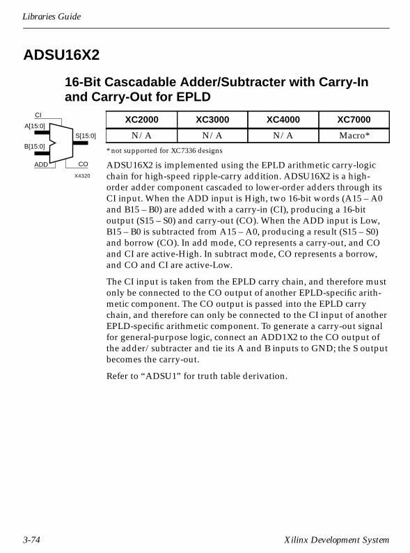
Libraries Guide
ADSU16X2
16-Bit Cascadable Adder/Subtracter with Carry-Inand Carry-Out for EPLD
* not supported for XC7336 designs
ADSU16X2 is implemented using the EPLD arithmetic carry-logicchain for high-speed ripple-carry addition. ADSU16X2 is a high-order adder component cascaded to lower-order adders through itsCI input. When the ADD input is High, two 16-bit words (A15 – A0and B15 – B0) are added with a carry-in (CI), producing a 16-bitoutput (S15 – S0) and carry-out (CO). When the ADD input is Low,B15 – B0 is subtracted from A15 – A0, producing a result (S15 – S0)and borrow (CO). In add mode, CO represents a carry-out, and COand CI are active-High. In subtract mode, CO represents a borrow,and CO and CI are active-Low.
The CI input is taken from the EPLD carry chain, and therefore mustonly be connected to the CO output of another EPLD-specific arith-metic component. The CO output is passed into the EPLD carrychain, and therefore can only be connected to the CI input of anotherEPLD-specific arithmetic component. To generate a carry-out signalfor general-purpose logic, connect an ADD1X2 to the CO output ofthe adder/subtracter and tie its A and B inputs to GND; the S outputbecomes the carry-out.
Refer to “ADSU1” for truth table derivation.
XC2000 XC3000 XC4000 XC7000
N/A N/A N/A Macro*A[15:0]
S[15:0]
ADD CO
CI
X4320
B[15:0]
3-74 Xilinx Development System
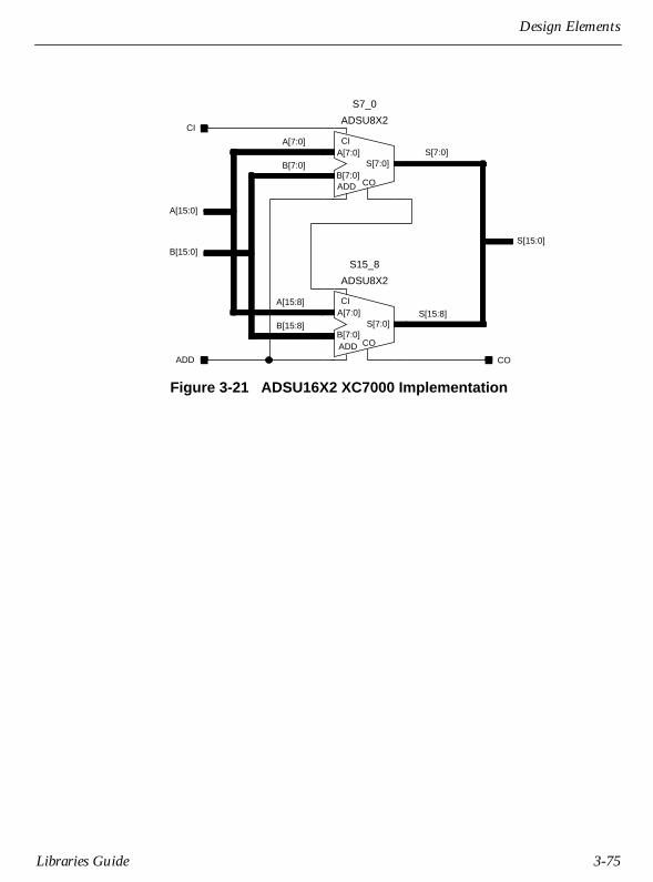
Design Elements
Figure 3-21 ADSU16X2 XC7000 Implementation
S15_8
ADSU8X2
ADD
CI
S[7:0]B[7:0]
A[7:0]
CO
S7_0
ADSU8X2
ADD
CI
S[7:0]B[7:0]
A[7:0]
CO
CI
CO
A[7:0]
A[15:8]
A[15:0]
B[15:8]
B[7:0]
B[15:0]
S[7:0]
S[15:8]
S[15:0]
ADD
Libraries Guide 3-75
Libraries Guide
AND
2- to 9-Input AND Gates with Inverted andNon-Inverted Inputs
The AND function is performed in the Configurable Logic Block(CLB) function generators for XC2000, XC3000, and XC4000 architec-tures. AND functions of up to five inputs are available in any combi-nation of inverting and non-inverting inputs. AND functions of six tonine inputs are available with only non-inverting inputs. To makesome or all inputs inverting, use external inverters. Because eachinput uses a CLB resource in FPGAs, replace functions with unusedinputs with functions having the appropriate number of inputs.
Available AND gates are shown in the following figure. Refer to theOverview chapter for the combinatorial/AND gate naming conven-tion.
Name XC2000 XC3000 XC4000 XC7000
AND2 – AND4B4 Primitive Primitive Primitive PrimitiveAND5 – AND5B5 Macro Primitive Primitive PrimitiveAND6, AND7, AND8, AND9 Macro Macro Macro Primitive
3-76 Xilinx Development System

Design Elements
Figure 3-22 AND Gate Representations
AND2B1
AND2B2
AND3
AND3B1
AND3B2
AND3B3
AND4
AND4B2
AND4B3
AND4B4
AND5
AND5B1
AND5B2
AND5B3
AND5B5
AND6
AND7
AND8
AND9
AND4B1
AND2
AND5B4
Libraries Guide 3-77
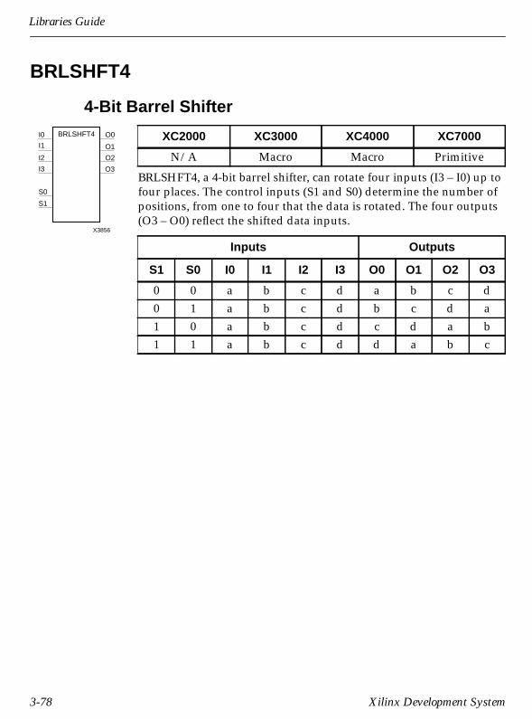
Libraries Guide
BRLSHFT4
4-Bit Barrel Shifter
BRLSHFT4, a 4-bit barrel shifter, can rotate four inputs (I3 – I0) up tofour places. The control inputs (S1 and S0) determine the number ofpositions, from one to four that the data is rotated. The four outputs(O3 – O0) reflect the shifted data inputs.
XC2000 XC3000 XC4000 XC7000
N/A Macro Macro Primitive
Inputs Outputs
S1 S0 I0 I1 I2 I3 O0 O1 O2 O3
0 0 a b c d a b c d0 1 a b c d b c d a1 0 a b c d c d a b1 1 a b c d d a b c
X3856
BRLSHFT4
S1
I2
I1
I0 O0
O3
O1
O2
I3
S0
3-78 Xilinx Development System

Design Elements
BRLSHFT8
8-Bit Barrel Shifter
BRLSHFT8, an 8-bit barrel shifter, can rotate the eight inputs, I7 – I0,up to eight places. The control inputs (S2 – S0) determine the numberof positions, from one to eight that the data is rotated. The eightoutputs (O7 – O0) reflect the shifted data inputs.
XC2000 XC3000 XC4000 XC7000
N/A Macro Macro Primitive
Inputs Output
S2 S1 S0 I0 I1 I2 I3 I4 I5 I6 I7 O0 O1 O2 O3 O4 O5 O6 O7
0 0 0 a b c d e f g h a b c d e f g h0 0 1 a b c d e f g h b c d e f g h a0 1 0 a b c d e f g h c d e f g h a b0 1 1 a b c d e f g h d e f g h a b c1 0 0 a b c d e f g h e f g h a b c d1 0 1 a b c d e f g h f g h a b c d e1 1 0 a b c d e f g h g h a b c d e f1 1 1 a b c d e f g h h a b c d e f g
X3857
BRLSHFT8
S2
O4
O7
O5
O6
O0
O3
O1
O2
I6
I5
I4
I7
I2
I1
I0
I3
S0
S1
Libraries Guide 3-79
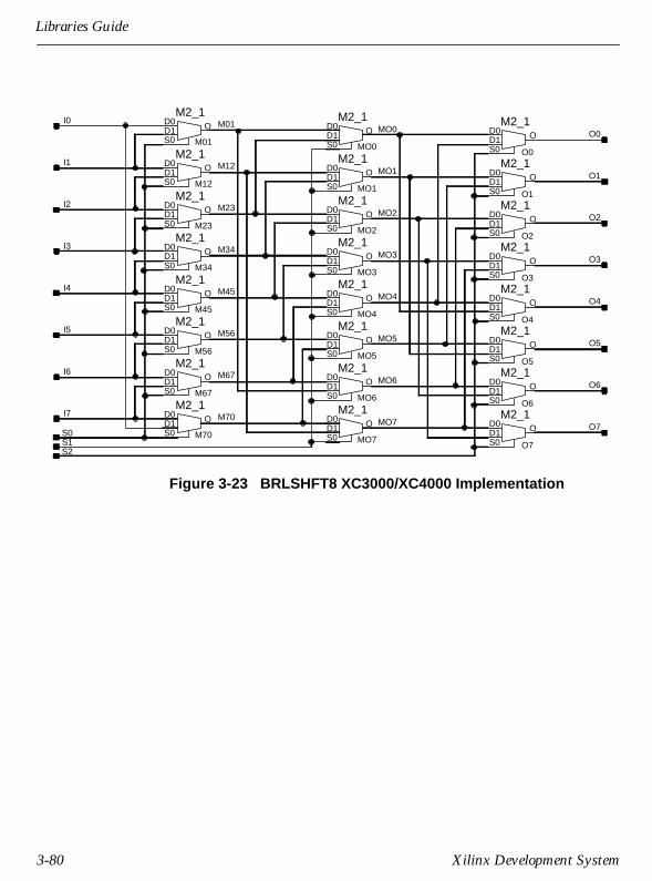
Libraries Guide
Figure 3-23 BRLSHFT8 XC3000/XC4000 Implementation
O0
D0D1 O
S0
M2_1
O1
D0D1 O
S0
M2_1
O7
D0D1 O
S0
M2_1O6
D0D1 O
S0
M2_1O5
D0D1 O
S0
M2_1O4
D0D1 O
S0
M2_1O3
D0D1 O
S0
M2_1O2
D0D1 O
S0
M2_1
M45
D0D1 O
S0
M2_1
M56
D0D1 O
S0
M2_1
M67
D0D1 O
S0
M2_1
M34
D0D1 O
S0
M2_1
M01
D0D1 O
S0
M2_1
M12
D0D1 O
S0
M2_1
M23
D0D1 O
S0
M2_1
O0
MO4
MO5
MO6
MO7 O7
O6
O5
O4
O3
O2
O1M12
M34
M45
M23
M56
M67
M70
S0
MO0
I1
I2
I3
I4
I5
I6
I7
MO3
MO2
MO7
D0D1 O
S0
M2_1
S1S2
M70
D0D1 O
S0
M2_1
I0 M01
MO1
MO0
D0D1 O
S0
M2_1
MO1
D0D1 O
S0
M2_1
MO2
D0D1 O
S0
M2_1
MO3
D0D1 O
S0
M2_1
MO4
D0D1 O
S0
M2_1
MO5
D0D1 O
S0
M2_1
MO6
D0D1 O
S0
M2_1
3-80 Xilinx Development System

Design Elements
BSCAN
Boundary Scan Logic Control Circuit
The BSCAN symbol indicates that boundary scan logic should beenabled after PLD configuration is complete. It also provides optionalaccess to some special features of the XC4000 boundary scan logic.An overview of the boundary scan interface follows, for completedetails, refer to the application note “Boundary Scan in XC4000Devices” in the Programmable Logic Data Book.
To indicate that boundary scan remain enabled after configuration,connect the BSCAN symbol to the TDI, TMS, TCK, and TDO padsshown in the following figure. The other pins on BSCAN do not needto be connected, unless those special functions are needed. A signalon the TDO1 input is passed to the external TDO output when theUSER1 instruction is executed; the SEL1 output goes High to indicatethat the USER1 instruction is active. The TDO2 and SEL2 pinsperform a similar function for the USER2 instruction. The DRCKoutput provides access to the data register clock (generated by theTAP controller). The IDLE output provides access to a version of theTCK input, which is only active while the TAP controller is in theRun-Test-Idle state.
If boundary scan is used only before configuration is complete, donot include the BSCAN symbol in the design, so the TDI, TMS, TCK,and TDO pins can be used for user functions.
XC2000 XC3000 XC4000 XC7000
N/A N/A Primitive N/A
X3910
TDO2
TDO1
TCK
TMS
SEL2
BSCANTDI
SEL1
IDLE
DRCK
TDO
X4323
BSCAN
TDO1
TDO2
TDO
IDLE
DRCK
SEL2
SEL1
TDI
TMS
TCK ToUserLogicFrom
UserLogic
Libraries Guide 3-81

Libraries Guide
BUF, BUF4, BUF8, and BUF16
General-Purpose Buffers
BUF is a general purpose, non-inverting buffer. In FPGA architecture,BUF is usually not necessary and is removed by the partitioning soft-ware (XNFMap for XC2000/XC3000 and PPR for XC4000). The BUFelement can be preserved for reducing the delay on a high fan-outnet, for example, by splitting the net and reducing capacitive loading.In this case, the buffer is preserved by attaching an X (explicit)attribute to both the input and output nets of the BUF.
In EPLD architecture, BUF is usually removed, unless you inhibitoptimization by applying the OPT=OFF attribute to the BUF symbolor by using the LOGIC_OPT=OFF global attribute.
Name XC2000 XC3000 XC4000 XC7000
BUF Primitive Primitive Primitive PrimitiveBUF4, BUF8, BUF16 N/A N/A N/A Primitive
X3830
X4614
BUF4
BUF8
X4615
BUF16
X4616
3-82 Xilinx Development System

Design Elements
BUFCE
Global Clock-Enable Buffer for EPLD
* not supported for XC7236, XC7272, or XC7336 designs
BUFCE, an EPLD-specific global buffer, distributes global clock-enable signals throughout the input-pad registers of an EPLD device.Global clock-enable pins are available on most XC7300 series devices;consult device data sheets for applicability.
BUFCE always acts as an input buffer. To use it in a schematic,connect the input of the BUFCE symbol to an IPAD or an IOPAD thatrepresents the clock-enable signal source. Clock-enable signals gener-ated on-chip must be passed through an OBUF-type buffer beforethey are connected to a BUFCE. The output of a BUFCE can only beconnected to the CE input of an EPLD-specific input-pad registersymbol, IFDX1. Each BUFCE can drive any number of IFDX1 regis-ters in a design. The CE input of IFDX1 is active-Low and cannot beinverted.
XC2000 XC3000 XC4000 XC7000
N/A N/A N/A Primitive*X4209
Libraries Guide 3-83

Libraries Guide
BUFE, BUFE4, BUFE8, and BUFE16
Internal 3-State Buffers
BUFE, BUFE4, BUFE8, and BUFE16 are single or multiple 3-statebuffers with inputs I, I3 – I0, I7 – I0, and so forth; outputs O, O3 – O0,O7 – O0, and so forth; and active-High output enable (E). When E isHigh, data on the inputs of the buffers is transferred to the corre-sponding outputs. When E is Low, the output is high impedance(Z state or off). The outputs of the buffers are connected to horizontallonglines in FPGA architectures.
The outputs of separate BUFE symbols can be tied together to form abus or a multiplexer. Make sure that only one E is High at one time. Ifnone of the E inputs is active-High, a “weak-keeper” circuit (FPGA)keeps the output bus from floating, but does not guarantee that thebus remains at the last value driven onto it.
The E in XC3000/XC4000 BUFE macros is implemented by using aBUFT with an inverter on the active-Low enable (T) pin. This invertercan add an extra level of logic to the data path. Pull-up resistors canbe used to establish a High logic level if all BUFE elements are off.Pull-up resistors are always assumed for EPLD designs. Thefollowing figure shows BUFE XC3000/XC4000 implementation.
Figure 3-24 BUFE XC3000/XC4000 Implementation
XC2000 XC3000 XC4000 XC7000
N/A Macro Macro Primitive
BUFE
X3790
E
X3797
BUFE4
E
BUFE8
X3809
E
BUFE16
X3821
E
BUFT
X4716
TE
I O
3-84 Xilinx Development System
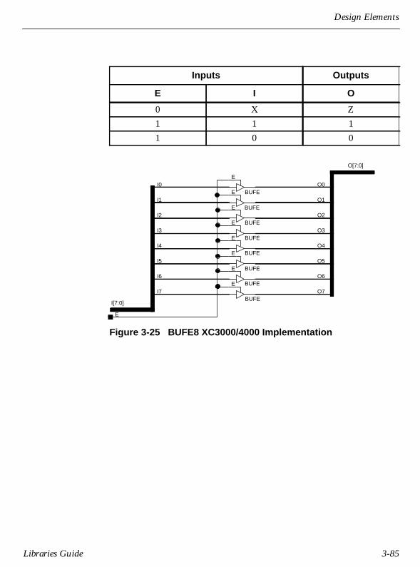
Design Elements
Figure 3-25 BUFE8 XC3000/4000 Implementation
Inputs Outputs
E I O
0 X Z1 1 11 0 0
E
I[7:0]
I7
I6
I5
I4
I3
I2
I1
I0
O7
O5
O4
O3
O2
O1
O0
O[7:0]
O6BUFE
E BUFE
E BUFE
E BUFE
E BUFE
E BUFE
E BUFE
E
BUFE
E
Libraries Guide 3-85

Libraries Guide
BUFFOE
Global Fast Output Enable Buffer for EPLD
* not supported for XC7272 designs
BUFFOE, an EPLD-specific global buffer, distributes global output-enable signals throughout the output pad drivers of an EPLD device.Global Fast Output Enable (FOE) pins are available on most XC7000architecture devices; consult device data sheets for applicability.
BUFFOE always acts as an input buffer. To use it in a schematic,connect the input of the BUFFOE symbol to an IPAD or an IOPADrepresenting the FOE signal source. FOE signals generated on-chipmust be passed through an OBUF-type buffer before they areconnected to the BUFFOE. The output of a BUFFOE can only connectto the E input of an EPLD-specific 3-state output buffer symbol,OBUFEX1. Each BUFFOE can drive any number of OBUFEX1 buffersin a design. The E input of OBUFEX1 is active-High and cannot beinverted.
XC2000 XC3000 XC4000 XC7000
N/A N/A N/A Primitive*X4210
3-86 Xilinx Development System
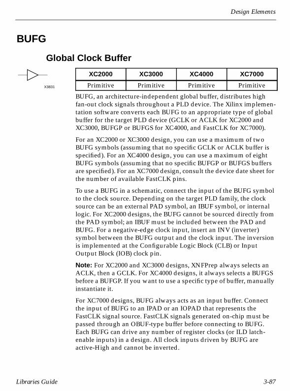
Design Elements
BUFG
Global Clock Buffer
BUFG, an architecture-independent global buffer, distributes highfan-out clock signals throughout a PLD device. The Xilinx implemen-tation software converts each BUFG to an appropriate type of globalbuffer for the target PLD device (GCLK or ACLK for XC2000 andXC3000, BUFGP or BUFGS for XC4000, and FastCLK for XC7000).
For an XC2000 or XC3000 design, you can use a maximum of twoBUFG symbols (assuming that no specific GCLK or ACLK buffer isspecified). For an XC4000 design, you can use a maximum of eightBUFG symbols (assuming that no specific BUFGP or BUFGS buffersare specified). For an XC7000 design, consult the device date sheet forthe number of available FastCLK pins.
To use a BUFG in a schematic, connect the input of the BUFG symbolto the clock source. Depending on the target PLD family, the clocksource can be an external PAD symbol, an IBUF symbol, or internallogic. For XC2000 designs, the BUFG cannot be sourced directly fromthe PAD symbol; an IBUF must be included between the PAD andBUFG. For a negative-edge clock input, insert an INV (inverter)symbol between the BUFG output and the clock input. The inversionis implemented at the Configurable Logic Block (CLB) or InputOutput Block (IOB) clock pin.
Note: For XC2000 and XC3000 designs, XNFPrep always selects anACLK, then a GCLK. For XC4000 designs, it always selects a BUFGSbefore a BUFGP. If you want to use a specific type of buffer, manuallyinstantiate it.
For XC7000 designs, BUFG always acts as an input buffer. Connectthe input of BUFG to an IPAD or an IOPAD that represents theFastCLK signal source. FastCLK signals generated on-chip must bepassed through an OBUF-type buffer before connecting to BUFG.Each BUFG can drive any number of register clocks (or ILD latch-enable inputs) in a design. All clock inputs driven by BUFG areactive-High and cannot be inverted.
XC2000 XC3000 XC4000 XC7000
Primitive Primitive Primitive PrimitiveX3831
Libraries Guide 3-87

Libraries Guide
BUFGP
Primary Global Buffer for Driving Clocks orLonglines (Four per PLD Device)
BUFGP, a primary global buffer, is used to distribute high fan-outclock or control signals throughout PLD devices. In XC7000 EPLDdesigns, BUFGP is treated like BUFG. A BUFGP provides directaccess to Configurable Logic Block (CLB) and Input Output Block(IOB) clock pins and limited access to other CLB inputs. FourBUFGPs are available on each XC4000 device, one in each corner. Theinput to a BUFGP comes only from a dedicated IOB.
Alongside each column of CLBs in an XC4000 device are four globalvertical lines, which are in addition to the standard vertical longlines.Each one of the four global vertical lines can drive the CLB clock (K)pin directly. In addition, one of the four lines can drive the F3 pin, asecond line can drive the G1 pin, a third can drive the C3 pin, and afourth can drive the C1 pin. Each of the four BUFGPs drives one ofthese global vertical lines. These same vertical lines are also used forthe secondary global buffers (refer to “BUFGS” for more informa-tion).
Because of its structure, a BUFGP can always access a clock pindirectly. However, it can access only one of the F3, G1, C3, or C1 pins,depending on the corner in which the BUFGP is placed. When therequired pin cannot be accessed directly from the vertical line, PPRfeeds the signal through another CLB and uses general purposerouting to access the load pin.
To use a BUFGP in a schematic, connect the input of the BUFGPelement directly to the PAD symbol. Do not use any IBUFs, becausethe signal comes directly from a dedicated IOB. The output of theBUFGP is then used throughout the schematic. For a negative-edgeclock, insert an INV (inverter) element between the output of theBUFGP and the clock input. This inversion is performed inside eachCLB or IOB.
XC2000 XC3000 XC4000 XC7000
N/A N/A Primitive PrimitiveX3902
3-88 Xilinx Development System

Design Elements
A BUFGP can be sourced by an internal signal, but PPR must use thededicated IOB to drive the BUFGP, which means that the IOB is notavailable for use by other signals. If possible, use a BUFGS instead,because they can be sourced internally without using an IOB.
The dedicated inputs for BUFGPs are identified by the names PGCK1through PGCK4 in XC4000 pinouts. The package pin that drives theBUFGP depends on which corner the BUFGP is placed by PPR.
Libraries Guide 3-89
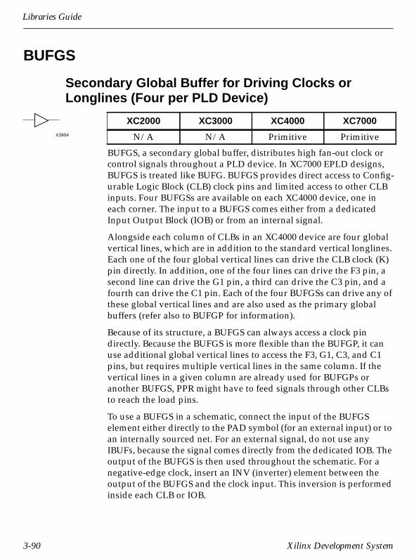
Libraries Guide
BUFGS
Secondary Global Buffer for Driving Clocks orLonglines (Four per PLD Device)
BUFGS, a secondary global buffer, distributes high fan-out clock orcontrol signals throughout a PLD device. In XC7000 EPLD designs,BUFGS is treated like BUFG. BUFGS provides direct access to Config-urable Logic Block (CLB) clock pins and limited access to other CLBinputs. Four BUFGSs are available on each XC4000 device, one ineach corner. The input to a BUFGS comes either from a dedicatedInput Output Block (IOB) or from an internal signal.
Alongside each column of CLBs in an XC4000 device are four globalvertical lines, which are in addition to the standard vertical longlines.Each one of the four global vertical lines can drive the CLB clock (K)pin directly. In addition, one of the four lines can drive the F3 pin, asecond line can drive the G1 pin, a third can drive the C3 pin, and afourth can drive the C1 pin. Each of the four BUFGSs can drive any ofthese global vertical lines and are also used as the primary globalbuffers (refer also to BUFGP for information).
Because of its structure, a BUFGS can always access a clock pindirectly. Because the BUFGS is more flexible than the BUFGP, it canuse additional global vertical lines to access the F3, G1, C3, and C1pins, but requires multiple vertical lines in the same column. If thevertical lines in a given column are already used for BUFGPs oranother BUFGS, PPR might have to feed signals through other CLBsto reach the load pins.
To use a BUFGS in a schematic, connect the input of the BUFGSelement either directly to the PAD symbol (for an external input) or toan internally sourced net. For an external signal, do not use anyIBUFs, because the signal comes directly from the dedicated IOB. Theoutput of the BUFGS is then used throughout the schematic. For anegative-edge clock, insert an INV (inverter) element between theoutput of the BUFGS and the clock input. This inversion is performedinside each CLB or IOB.
XC2000 XC3000 XC4000 XC7000
N/A N/A Primitive PrimitiveX3904
3-90 Xilinx Development System

Design Elements
The dedicated inputs for BUFGSs are identified by the names SGCK1through SGCK4 in XC4000 pinouts. The package pin that drives theBUFGS depends on which corner the BUFGS is placed by PPR.
Libraries Guide 3-91

Libraries Guide
BUFOD
Open-Drain Buffer
BUFOD is a buffer with input (I) and open-drain output (O). Whenthe input is Low, the output is Low. When the input is High, theoutput is off. To establish an output High level, a pull-up resistors istied to output O. One pull-up resistor uses the least power; two pull-up resistors achieve the fastest Low-to-High speed.
To indicate two pull-up resistors, append a DOUBLE parameter tothe pull-up symbol attached to the output (O) node. Refer to theappropriate CAE tool interface user guide for details.
Figure 3-26 BUFOD XC4000 Implementation
XC2000 XC3000 XC4000 XC7000
N/A N/A Macro N/AX3903
WAND1
OI
3-92 Xilinx Development System
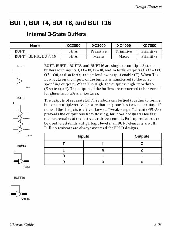
Design Elements
BUFT, BUFT4, BUFT8, and BUFT16
Internal 3-State Buffers
BUFT, BUFT4, BUFT8, and BUFT16 are single or multiple 3-statebuffers with inputs I, I3 – I0, I7 – I0, and so forth; outputs O, O3 – O0,O7 – O0, and so forth; and active-Low output enable (T). When T isLow, data on the inputs of the buffers is transferred to the corre-sponding outputs. When T is High, the output is high impedance(Z state or off). The outputs of the buffers are connected to horizontallonglines in FPGA architectures.
The outputs of separate BUFT symbols can be tied together to form abus or a multiplexer. Make sure that only one T is Low at one time. Ifnone of the T inputs is active (Low), a “weak-keeper” circuit (FPGAs)prevents the output bus from floating, but does not guarantee thatthe bus remains at the last value driven onto it. Pull-up resistors canbe used to establish a High logic level if all BUFT elements are off.Pull-up resistors are always assumed for EPLD designs.
Name XC2000 XC3000 XC4000 XC7000
BUFT N/A Primitive Primitive PrimitiveBUFT4, BUFT8, BUFT16 N/A Macro Macro Primitive
Inputs Outputs
T I O
1 X Z0 1 10 0 0
BUFT
X3789
T
X3796
BUFT4
T
BUFT8
X3808
T
BUFT16
X3820
T
Libraries Guide 3-93

Libraries Guide
Figure 3-27 BUFT8 XC3000/4000 Implementation
O6
O[7:0]
O0
O1
O2
O3
O4
O5
O7
I0
I1
I2
I3
I4
I5
I6
I7
I[7:0]BUFT
T
BUFT
T
BUFT
T
BUFT
T
BUFT
T
BUFT
T
BUFT
T
BUFT
T
T
3-94 Xilinx Development System

Design Elements
CB2CE
2-Bit Cascadable Binary Counter with Clock Enableand Asynchronous Clear
CB2CE is a 2-stage, 2-bit, synchronous, clearable, cascadable binarycounter. The asynchronous clear (CLR) is the highest priority input.When CLR is High, all other inputs are ignored and data (Q1 – Q0)and terminal count (TC) outputs go to logic level zero, independentof clock transitions. The outputs (Q1 – Q0) increment when the clockenable input (CE) is High during the Low-to-High clock (C) transi-tion. The counter ignores clock transitions when CE is Low. The TCoutput is High when both Q outputs are High.
Larger counters are created by connecting the count enable out (CEO)output of the first stage to the CE input of the next stage andconnecting the C and CLR inputs in parallel. CEO is active (High)when TC and CE are High. The maximum length of the counter isdetermined by the accumulated CE-to-TC propagation delays versusthe clock period. The clock period must be greater than n(tCE-TC),where “n” is the number of stages and “tCE-TC” is the CE-to-TCpropagation delay of each stage.
The counter is asynchronously reset, output Low, when power isapplied or when global reset (GR for XC2000, XC3000) or globalset/reset (GSR for XC4000) is active. GR is active-Low; the GSR activelevel is programmable. When cascading counters, use the CEOoutput if the counter uses the CE input; use the TC output if it doesnot.
XC2000 XC3000 XC4000 XC7000
Macro Macro Macro PrimitiveQ1
X4353CLR
C
CB2CE
CE CEO
TC
Q0
Libraries Guide 3-95

Libraries Guide
TC = (Q1•Q0)
CEO = (TC•CE)
Inputs Outputs
CLR CE C Q1 – Q0 TC CEO
1 X X 0 0 00 0 X No Chg No Chg 00 1 ↑ Inc TC CEO
3-96 Xilinx Development System
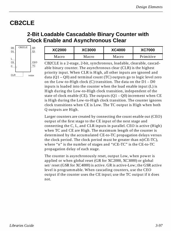
Design Elements
CB2CLE
2-Bit Loadable Cascadable Binary Counter withClock Enable and Asynchronous Clear
CB2CLE is a 2-stage, 2-bit, synchronous, loadable, clearable, cascad-able binary counter. The asynchronous clear (CLR) is the highestpriority input. When CLR is High, all other inputs are ignored anddata (Q1 – Q0) and terminal count (TC) outputs go to logic level zeroon the Low-to-High clock (C) transition. The data on the D1 – D0inputs is loaded into the counter when the load enable input (L) isHigh during the Low-to-High clock transition, independent of thestate of clock enable (CE). The outputs (Q1 – Q0) increment when CEis High during the Low-to-High clock transition. The counter ignoresclock transitions when CE is Low. The TC output is High when bothQ outputs are High.
Larger counters are created by connecting the count enable out (CEO)output of the first stage to the CE input of the next stage andconnecting the C, L, and CLR inputs in parallel. CEO is active (High)when TC and CE are High. The maximum length of the counter isdetermined by the accumulated CE-to-TC propagation delays versusthe clock period. The clock period must be greater than n(tCE-TC),where “n” is the number of stages and “tCE-TC” is the CE-to-TCpropagation delay of each stage.
The counter is asynchronously reset, output Low, when power isapplied or when global reset (GR for XC2000, XC3000) or globalset/reset (GSR for XC4000) is active. GR is active-Low; the GSR activelevel is programmable. When cascading counters, use the CEOoutput if the counter uses the CE input; use the TC output if it doesnot.
XC2000 XC3000 XC4000 XC7000
Macro Macro Macro Primitive
Q0
X4354
CB2CLE
C
CLR
CE
Q1
TC
CEO
L
D1
D0
Libraries Guide 3-97

Libraries Guide
TC = (Q1•Q0)
CEO = (TC•CE)
dn = state of referenced input one set-up time prior to active clock transition
Inputs Outputs
CLR L CE C D1 – D0 Q1 – Q0 TC CEO
1 X X X X 0 0 00 1 X ↑ D d1 – d0 TC CEO0 0 0 X X No Chg No Chg 00 0 1 ↑ X Inc TC CEO
3-98 Xilinx Development System

Design Elements
CB2CLED
2-Bit Loadable Cascadable Bidirectional BinaryCounter with Clock Enable and Asynchronous Clear
CB2CLED is a 2-stage, 2-bit, synchronous, loadable, clearable, cascad-able, bidirectional binary counter. The asynchronous clear (CLR) isthe highest priority input. When CLR is High, all other inputs areignored and data (Q1 – Q0) and terminal count (TC) outputs go tologic level zero, independent of clock transitions. The data on theD1 – D0 inputs is loaded into the counter when the load enable input(L) is High during the Low-to-High clock (C) transition, independentof the state of clock enable (CE). The outputs (Q1 – Q0) decrementwhen CE is High and UP is Low during the Low-to-High clock tran-sition. The outputs (Q1 – Q0) increment when CE and UP are High.The counter ignores clock transitions when CE is Low.
For counting up, the TC output is High when all Q outputs and UPare High. For counting down, the TC output is High when all Qoutputs and UP are Low. To cascade counters, the clock enable out(CEO) output of each counter is connected to the CE pin of the nextstage. The clock, UP, L, and CLR inputs are connected in parallel.CEO is active (High) when TC and CE are High. The maximumlength of the counter is determined by the accumulated CE-to-TCpropagation delays versus the clock period. The clock period must begreater than n(tCE-TC), where “n” is the number of stages and“tCE-TC” is the CE-to-TC propagation delay of each stage. For EPLDdesigns, refer to “CB2X1” for high-performance cascadable, bidirec-tional counters.
The counter is asynchronously reset, output Low, when power isapplied or when global reset (GR for XC2000, XC3000) or globalset/reset (GSR for XC4000) is active. GR is active-Low; the GSR activelevel is programmable. When cascading counters, use the CEOoutput if the counter uses the CE input; use the TC output if it doesnot.
XC2000 XC3000 XC4000 XC7000
Macro Macro Macro Primitive
Q0
X4355
CB2CLED
C
CLR
CE
TC
CEO
Q1
L
UP
D1
D0
Libraries Guide 3-99

Libraries Guide
TC = (Q1•Q0•UP) + (Q1•Q0•UP)
CEO = (TC•CE)
dn = state of referenced input one set-up time prior to active clock transition
Inputs Outputs
CLR L CE C UP D1 – D0 Q1 – Q0 TC CEO
1 X X X X X 0 0 00 1 X ↑ X D d1 – d0 TC CEO0 0 0 X X X No Chg No Chg 00 0 1 ↑ 1 X Inc TC CEO0 0 1 ↑ 0 X Dec TC CEO
3-100 Xilinx Development System

Design Elements
CB2RE
2-Bit Cascadable Binary Counter with Clock Enableand Synchronous Reset
CB2RE is a 2-stage, 2-bit, synchronous, resettable, cascadable binarycounter. The synchronous reset (R) is the highest priority input.When R is High, all other inputs are ignored and data (Q1 – Q0) andterminal count (TC) outputs go to logic level zero, independent ofclock transitions. The outputs (Q1 – Q0) increment when the clockenable input (CE) is High during the Low-to-High clock (C) transi-tion. The counter ignores clock transitions when CE is Low. The TCoutput is High when both Q outputs are High.
Larger counters are created by connecting the count enable out (CEO)output of the first stage to the CE input of the next stage andconnecting the C and R inputs in parallel. CEO is active (High) whenTC and CE are High. The maximum length of the counter is deter-mined by the accumulated CE-to-TC propagation delays versus theclock period. The clock period must be greater than n(tCE-TC), where“n” is the number of stages and “tCE-TC” is the CE-to-TC propaga-tion delay of each stage.
The counter is asynchronously reset, output Low, when power isapplied or when global reset (GR for XC2000, XC3000) or globalset/reset (GSR for XC4000) is active. GR is active-Low; the GSR activelevel is programmable. When cascading counters, use the CEOoutput if the counter uses the CE input; use the TC output if it doesnot.
XC2000 XC3000 XC4000 XC7000
Macro Macro Macro PrimitiveQ1
X4356R
C
CB2RE
CE CEO
TC
Q0
Libraries Guide 3-101

Libraries Guide
TC = (Q1•Q0)
CEO = (TC•CE)
Inputs Outputs
R CE C Q1 – Q0 TC CEO
1 X ↑ 0 0 00 0 X No Chg No Chg 00 1 ↑ Inc TC CEO
3-102 Xilinx Development System

Design Elements
CB2RLE
2-Bit Loadable Cascadable Binary Counter withClock Enable and Synchronous Reset
CB2RLE is a 2-stage, 2-bit, synchronous, loadable, resettable, cascad-able binary counter. The synchronous reset (R) is the highest priorityinput. The synchronous R, when High, overrides all other inputs andresets the Q1 – Q0, terminal count (TC), and clock enable out (CEO)outputs to Low on the Low-to-High clock (C) transition.
The data on the D1 – D0 inputs is loaded into the counter when theload enable input (L) is High during the Low-to-High clock (C) tran-sition, independent of the state of CE. The outputs (Q1 – Q0) incre-ment when CE is High during the Low-to-High clock transition. Thecounter ignores clock transitions when CE is Low. The TC output isHigh when all Q outputs are High. The CEO output is High when allQ outputs and CE are High to allow direct cascading of counters.Larger counters are created by connecting the CEO output of the firststage to the CE input of the next stage and by connecting the C, L,and R inputs in parallel. The maximum length of the counter is deter-mined by the accumulated CE-to-CEO propagation delays versus theclock period.
The counter is asynchronously reset, output Low, when power isapplied or when global reset or master reset is active. Whencascading counters, use the CEO output if the counter uses the CEinput; use the TC output if it does not.
XC2000 XC3000 XC4000 XC7000
N/A N/A N/A Primitive
Q0
X4513
CB2RLE
C
R
CE
Q1
CEO
TC
L
D1
D0
Libraries Guide 3-103

Libraries Guide
TC = Q1•Q0
CEO = TC•CE
dn = state of referenced input one set-up time prior to active clock transition
Inputs Outputs
R L CE C D1 – D0 Q1 – Q0 TC CEO
1 X X ↑ X 0 0 00 1 X ↑ D d1 – d0 TC CEO0 0 0 X X No Chg No Chg 00 0 1 ↑ X Inc TC CEO
3-104 Xilinx Development System

Design Elements
CB2X1
2-Bit Loadable Cascadable Bidirectional BinaryCounter with Clock Enable and Asynchronous Clear
CB2X1 is a 2-stage, 2-bit, synchronous, loadable, clearable, bidirec-tional binary counter. CB2X1 has separate count-enable inputs andsynchronous terminal-count outputs for up and down directions tosupport high-speed cascading in the EPLD architecture.
The asynchronous clear (CLR) is the highest priority input. WhenCLR is High, all other inputs are ignored, data outputs (Q1 – Q0) goto logic level zero, and terminal count outputs TCU and TCD go tozero and one, respectively, independent of clock transitions. The dataon the D1 – D0 inputs loads into the counter on the Low-to-Highclock (C) transition when the load enable input (L) is High, indepen-dent of the CE inputs.
The outputs (Q1 – Q0) increment when CEU is High, provided CLRand L are Low, during the Low-to-High clock transition. The outputs(Q1 – Q0) decrement when CED is High, provided CLR and L areLow. The counter ignores clock transitions when CEU and CED areLow. Both CEU and CED should not be High during the same clocktransition; the CEOU and CEOD outputs might not function properlyfor cascading when CEU and CED are both High.
For counting up, the CEOU output is High when all Q outputs andCEU are High. For counting down, the CEOD output is High whenall Q outputs are Low and CED is High. To cascade counters, theCEOU and CEOD outputs of each counter are connected directly tothe CEU and CED inputs, respectively, of the next stage. The clock, Land CLR inputs are connected in parallel.
In Xilinx EPLD devices, the maximum clocking frequency of thesecounter components is unaffected by the number of cascaded stagesfor all counting and loading functions. The TCU terminal countoutput is High when all Q outputs are High, regardless of CEU. TheTCD output is High when all Q outputs are Low, regardless of CED.
XC2000 XC3000 XC4000 XC7000
N/A N/A N/A Primitive
X4194
CB2X1
C
D1
D0 QO
Q1
CEU
L
CED
CLR
TCU
TCD
CEOU
CEOD
Libraries Guide 3-105

Libraries Guide
When cascading counters, the final terminal count signals can beproduced by AND wiring all the TCU outputs (for the up direction)and all the TCD outputs (for the down direction). The TCU, CEOU,and CEOD outputs are produced by optimizable AND gates withinthe component, resulting in zero propagation from the CEU and CEDinputs and from the Q outputs, provided all connections from eachsuch output remain on-chip. Otherwise, a macrocell buffer delay isintroduced. The counter is initialized to zero (TCU Low and TCDHigh) when the device is powered-up or when the device MasterReset pin is activated. The clock (C) input can be driven by either theEPLD FastCLK global net (represented by a BUFG symbol), an ordi-nary input, or other on-chip logic.
TCU = Q1•Q0
TCD = Q1•Q0
CEOU = TCU•CEU
CEOD = TCD•CED
dn = state of referenced input one set-up time prior to active clock transition
Inputs Outputs
CLR L CEU CED C D1 – D0 Q1 – Q0 TCU TCD CEOU CEOD
1 X X X X X 0 0 1 0 CEOD0 1 X X ↑ D d1 – d0 TCU TCD CEOU CEOD0 0 0 0 X X No Chg No Chg No Chg 0 00 0 1 0 ↑ X Inc TCU TCD CEOU 00 0 0 1 ↑ X Dec TCU TCD 0 CEOD0 0 1 1 ↑ X Inc TCU TCD Invalid Invalid
3-106 Xilinx Development System

Design Elements
CB2X2
2-Bit Loadable Cascadable Bidirectional BinaryCounter with Clock Enable and Synchronous Reset
CB2X2 is a 2-stage, 2-bit, synchronous, loadable, resettable, bidirec-tional binary counter. CB2X2 has separate count-enable inputs andsynchronous terminal-count outputs for up and down directions tosupport high-speed cascading in the EPLD architecture.
The synchronous reset (R) is the highest priority input. When R isHigh, all other inputs are ignored, data outputs (Q1 – Q0) go to logiclevel zero, and terminal count outputs TCU and TCD go to zero andone, respectively, on the Low-to-High clock (C) transition. The dataon the D1 – D0 inputs loads into the counter on the Low-to-Highclock (C) transition when the load enable input (L) is High, indepen-dent of the CE inputs.
The outputs (Q1 – Q0) increment when CEU is High, provided R andL are Low during the Low-to-High clock transition. The outputs(Q1 – Q0) decrement when CED is High, provided R and L are Low.The counter ignores clock transitions when CEU and CED are Low.Both CEU and CED should not be High during the same clock transi-tion; the CEOU and CEOD outputs might not function properly forcascading when CEU and CED are both High.
For counting up, the CEOU output is High when all Q outputs andCEU are High. For counting down, the CEOD output is High whenall Q outputs are Low and CED is High. To cascade counters, theCEOU and CEOD outputs of each counter are connected directly tothe CEU and CED inputs, respectively, of the next stage. The C, L,and R inputs are connected in parallel.
In Xilinx EPLD devices, the maximum clocking frequency of thesecounter components is unaffected by the number of cascaded stagesfor all counting and loading functions. The TCU terminal countoutput is High when all Q outputs are High, regardless of CEU. TheTCD output is High when all Q outputs are Low, regardless of CED.
XC2000 XC3000 XC4000 XC7000
N/A N/A N/A Primitive
X4195
CB2X2
C
D1
D0 QO
Q1
CEU
L
CED
R
TCU
TCD
CEOU
CEOD
Libraries Guide 3-107

Libraries Guide
When cascading counters, the final terminal count signals can beproduced by AND wiring all the TCU outputs (for the up direction)and all the TCD outputs (for the down direction). The TCU, CEOU,and CEOD outputs are produced by optimizable AND gates withinthe component, resulting in zero propagation from the CEU and CEDinputs and from the Q outputs, provided all connections from eachsuch output remain on-chip. Otherwise, a macrocell buffer delay isintroduced. The counter is initialized to zero (TCU Low and TCDHigh) when power is applied or when the device Master Reset pin isactivated. The clock (C) input can be driven by either the EPLDFastCLK global net (represented by a BUFG symbol), an ordinaryinput, or other on-chip logic.
TCU = Q1•Q0
TCD = Q1•Q0
CEOU = TCU•CEU
CEOD = TCD•CED
dn = state of referenced input one set-up time prior to active clock transition
Inputs Outputs
R L CEU CED C D1 – D0 Q1 – Q0 TCU TCD CEOU CEOD
1 X X X ↑ X 0 0 1 0 CEOD0 1 X X ↑ D d1 – d0 TCU TCD CEOU CEOD0 0 0 0 X X No Chg No Chg No Chg 0 00 0 1 0 ↑ X Inc TCU TCD CEOU 00 0 0 1 ↑ X Dec TCU TCD 0 CEOD0 0 1 1 ↑ X Inc TCU TCD Invalid Invalid
3-108 Xilinx Development System

Design Elements
CB4CE
4-Bit Cascadable Binary Counter with Clock Enableand Asynchronous Clear
CB4CE is a 4-stage, 4-bit, synchronous, clearable, cascadable binarycounter. The asynchronous clear (CLR) is the highest priority input.When CLR is High, all other inputs are ignored and data (Q3 – Q0)and terminal count (TC) outputs go to logic level zero, independentof clock transitions. The outputs (Q3 – Q0) increment when the clockenable input (CE) is High during the Low-to-High clock (C) transi-tion. The counter ignores clock transitions when CE is Low. The TCoutput is High when all Q outputs are High.
Larger counters are created by connecting the count enable out (CEO)output of the first stage to the CE input of the next stage andconnecting the C and CLR inputs in parallel. CEO is active (High)when TC and CE are High. The maximum length of the counter isdetermined by the accumulated CE-to-TC propagation delays versusthe clock period. The clock period must be greater than n(tCE-TC),where “n” is the number of stages and “tCE-TC” is the CE-to-TCpropagation delay of each stage.
The counter is asynchronously reset, output Low, when power isapplied or when global reset (GR for XC2000, XC3000) or globalset/reset (GSR for XC4000) is active. GR is active-Low; the GSR activelevel is programmable. When cascading counters, use the CEOoutput if the counter uses the CE input; use the TC output if it doesnot.
XC2000 XC3000 XC4000 XC7000
Macro Macro Macro PrimitiveQ2
X4357
CB4CE
C
CLR
CE CEO
TC
Q1
Q0
Q3
Libraries Guide 3-109

Libraries Guide
TC = (Q3•Q2•Q1•Q0)
CEO = (TC•CE)
Inputs Outputs
CLR CE C Q3 – Q0 TC CEO
1 X X 0 0 00 0 X No Chg No Chg 00 1 ↑ Inc TC CEO
3-110 Xilinx Development System

Design Elements
CB4CLE
4-Bit Loadable Cascadable Binary Counter withClock Enable and Asynchronous Clear
CB4CLE is a 4-stage, 4-bit, synchronous, loadable, clearable, cascad-able binary counter. The asynchronous clear (CLR) is the highestpriority input. When CLR is High, all other inputs are ignored anddata (Q3 – Q0) and terminal count (TC) outputs go to logic level zero,independent of clock transitions. The data on the D3 – D0 inputs isloaded into the counter when the load enable input (L) is Highduring the Low-to-High clock (C) transition, independent of the stateof clock enable (CE). The outputs (Q3 – Q0) increment when CE isHigh during the Low-to-High clock transition. The counter ignoresclock transitions when CE is Low. The TC output is High when all Qoutputs are High.
Larger counters are created by connecting the count enable out (CEO)output of the first stage to the CE input of the next stage andconnecting the C, L, and CLR inputs in parallel. CEO is active (High)when TC and CE are High. The maximum length of the counter isdetermined by the accumulated CE-to-TC propagation delays versusthe clock period. The clock period must be greater than n(tCE-TC),where “n” is the number of stages and “tCE-TC” is the CE-to-TCpropagation delay of each stage.
The counter is asynchronously reset, output Low, when power isapplied or when global reset (GR for XC2000, XC3000) or globalset/reset (GSR for XC4000) is active. GR is active-Low; the GSR activelevel is programmable. When cascading counters, use the CEOoutput if the counter uses the CE input; use the TC output if it doesnot.
XC2000 XC3000 XC4000 XC7000
Macro Macro Macro Primitive
X4358
CB4CLE
L
CE
C
D3
D2
D1
D0
Q3
Q2
Q1
Q0
CLR
CEO
TC
Libraries Guide 3-111

Libraries Guide
TC = (Q3•Q2•Q1•Q0)
CEO = (TC•CE)
dn = state of referenced input one set-up time prior to active clock transition
Inputs Outputs
CLR L CE C D3 – D0 Q3 – Q0 TC CEO
1 X X X X 0 0 00 1 X ↑ D d3 – d0 TC CEO0 0 0 X X No Chg No Chg 00 0 1 ↑ X Inc TC CEO
3-112 Xilinx Development System

Design Elements
CB4CLED
4-Bit Loadable Cascadable Bidirectional BinaryCounter with Clock Enable and Asynchronous Clear
CB4CLED is a 4-stage, 4-bit, synchronous, loadable, clearable, cascad-able, bidirectional binary counter. The asynchronous clear (CLR) isthe highest priority input. When CLR is High, all other inputs areignored and data (Q3 – Q0) and terminal count (TC) outputs go tologic level zero, independent of clock transitions. The data on theD3 – D0 inputs is loaded into the counter when the load enable input(L) is High during the Low-to-High clock (C) transition, independentof the state of clock enable (CE). The outputs (Q3 – Q0) decrementwhen CE is High and UP is Low during the Low-to-High clock tran-sition. The outputs (Q3 – Q0) increment when CE and UP are High.The counter ignores clock transitions when CE is Low.
For counting up, the TC output is High when all Q outputs and UPare High. For counting down, the TC output is High when all Qoutputs and UP are Low. To cascade counters, the count enable out(CEO) output of each counter is connected to the CE pin of the nextstage. The clock, UP, L, and CLR inputs are connected in parallel.CEO is active (High) when TC and CE are High. The maximumlength of the counter is determined by the accumulated CE-to-TCpropagation delays versus the clock period. The clock period must begreater than n(tCE-TC), where “n” is the number of stages and“tCE-TC” is the CE-to-TC propagation delay of each stage. For EPLDdesigns, refer to “CB4X1” for high-performance cascadable, bidirec-tional counters.
The counter is asynchronously reset, output Low, when power isapplied or when global reset (GR for XC2000, XC3000) or globalset/reset (GSR for XC4000) is active. GR is active-Low; the GSR activelevel is programmable. When cascading counters, use the CEOoutput if the counter uses the CE input; use the TC output if it doesnot.
XC2000 XC3000 XC4000 XC7000
Macro Macro Macro Primitive
X4359
CB4CLED
L
CE
C
D3
D2
D1
D0
Q3
Q2
Q1
Q0
CLR
CEO
TC
UP
Libraries Guide 3-113
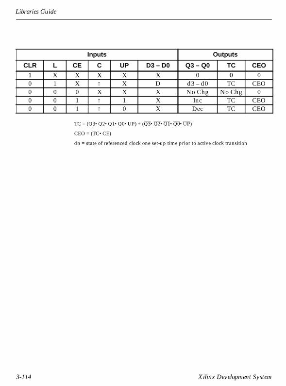
Libraries Guide
TC = (Q3•Q2•Q1•Q0•UP) + (Q3•Q2•Q1•Q0•UP)
CEO = (TC•CE)
dn = state of referenced clock one set-up time prior to active clock transition
Inputs Outputs
CLR L CE C UP D3 – D0 Q3 – Q0 TC CEO
1 X X X X X 0 0 00 1 X ↑ X D d3 – d0 TC CEO0 0 0 X X X No Chg No Chg 00 0 1 ↑ 1 X Inc TC CEO0 0 1 ↑ 0 X Dec TC CEO
3-114 Xilinx Development System

Design Elements
CB4RE
4-Bit Cascadable Binary Counter with Clock Enableand Synchronous Reset
CB4CE is a 4-stage, 4-bit, synchronous, resettable, cascadable binarycounter. The synchronous reset (R) is the highest priority input.When R is High, all other inputs are ignored and data (Q3 – Q0) andterminal count (TC) outputs go to logic level zero on the Low-to-Highclock (C) transition. The outputs (Q3 – Q0) increment when the clockenable input (CE) is High during the Low-to-High clock transition.The counter ignores clock transitions when CE is Low. The TC outputis High when all Q outputs are High.
Larger counters are created by connecting the count enable out (CEO)output of the first stage to the CE input of the next stage andconnecting the C and R inputs in parallel. CEO is active (High) whenTC and CE are High. The maximum length of the counter is deter-mined by the accumulated CE-to-TC propagation delays versus theclock period. The clock period must be greater than n(tCE-TC), where“n” is the number of stages and “tCE-TC” is the CE-to-TC propaga-tion delay of each stage.
The counter is asynchronously reset, output Low, when power isapplied or when global reset (GR for XC2000, XC3000) or globalset/reset (GSR for XC4000) is active. GR is active-Low; the GSR activelevel is programmable. When cascading counters, use the CEOoutput if the counter uses the CE input; use the TC output if it doesnot.
XC2000 XC3000 XC4000 XC7000
Macro Macro Macro PrimitiveQ2
X4360
CB4RE
C
R
CE
Q3
TC
Q1
Q0
CEO
Libraries Guide 3-115

Libraries Guide
TC = (Q3•Q2•Q2•Q0)
CEO = (TC•CE)
Inputs Outputs
R CE C Q3 – Q0 TC CEO
1 X ↑ 0 0 00 0 X No Chg No Chg 00 1 ↑ Inc TC CEO
3-116 Xilinx Development System

Design Elements
CB4RLE
4-Bit Loadable Cascadable Binary Counter withClock Enable and Synchronous Reset
CB4RLE is a 4-stage, 4-bit, synchronous, loadable, resettable, cascad-able binary counter. The synchronous reset (R) is the highest priorityinput. The synchronous R, when High, overrides all other inputs andresets the Q3 – Q0, TC, and CEO outputs to Low on the Low-to-Highclock (C) transition. The data on the D3 – D0 inputs is loaded into thecounter when the load enable input (L) is High during the Low-to-High clock (C) transition, independent of the state of CE. The outputs(Q3 – Q0) increment when CE is High during the Low-to-High clocktransition. The counter ignores clock transitions when CE is Low. TheTC output is High when all Q outputs are High. The CEO output isHigh when all Q outputs and CE are High to allow direct cascadingof counters.
Larger counters are created by connecting the CEO output of the firststage to the CE input of the next stage and by connecting the C, L,and R inputs in parallel. The maximum length of the counter is deter-mined by the accumulated CE-to-CEO propagation delays versus theclock period.
The counter is asynchronously reset, output Low, when power isapplied or when global reset or master reset is active. Whencascading counters, use the CEO output if the counter uses the CEinput; use the TC output if it does not.
XC2000 XC3000 XC4000 XC7000
N/A N/A N/A Primitive
X4514
CB4RLE
C
R
CE CEO
TC
Q3
L
D3
D2
D1
D0
Q2
Q1
Q0
Libraries Guide 3-117
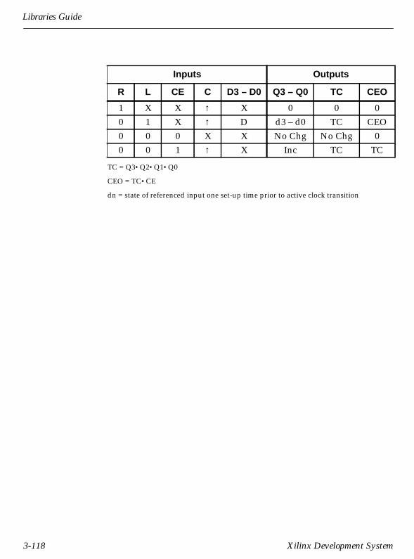
Libraries Guide
TC = Q3•Q2•Q1•Q0
CEO = TC•CE
dn = state of referenced input one set-up time prior to active clock transition
Inputs Outputs
R L CE C D3 – D0 Q3 – Q0 TC CEO
1 X X ↑ X 0 0 00 1 X ↑ D d3 – d0 TC CEO0 0 0 X X No Chg No Chg 00 0 1 ↑ X Inc TC TC
3-118 Xilinx Development System

Design Elements
CB4X1
4-Bit Loadable Cascadable Bidirectional BinaryCounter with Clock Enable and Asynchronous Clear
CB4X1 is a 4-stage, 4-bit, synchronous, loadable, clearable, bidirec-tional binary counter. CB4X1 has separate count-enable inputs andsynchronous terminal-count outputs for up and down directions, tosupport high-speed cascading in the EPLD architecture.
The asynchronous clear (CLR) is the highest priority input. WhenCLR is High, all other inputs are ignored, data outputs (Q3 – Q0) goto logic level zero, and terminal count outputs TCU and TCD go tozero and one, respectively, independent of clock transitions. The dataon the D3 – D0 inputs loads into the counter on the Low-to-Highclock (C) transition when the load enable input (L) is High, indepen-dent of the CE inputs.
The outputs (Q3 – Q0) increment when CEU is High, provided CLRand L are Low, during the Low-to-High clock transition. The outputs(Q3 – Q0) decrement when CED is High, provided CLR and L areLow. The counter ignores clock transitions when CEU and CED areLow. Both CEU and CED should not be High during the same clocktransition; the CEOU and CEOD outputs might not function properlyfor cascading when CEU and CED are both High.
For counting up, the CEOU output is High when all Q outputs andCEU are High. For counting down, the CEOD output is High whenall Q outputs are Low and CED is High. To cascade counters, theCEOU and CEOD outputs of each counter are connected directly tothe CEU and CED inputs, respectively, of the next stage. The clock, L,and CLR inputs are connected in parallel.
In Xilinx EPLD devices, the maximum clocking frequency of thesecounter components is unaffected by the number of cascaded stagesfor all counting and loading functions. The TCU terminal countoutput is High when all Q outputs are High, regardless of CEU. TheTCD output is High when all Q outputs are Low, regardless of CED.
XC2000 XC3000 XC4000 XC7000
N/A N/A N/A Primitive
X4196
CB4X1
C
Q2
Q3
CEU
L
CED
CLR
TCU
TCD
CEOU
CEOD
D3
D0
D2
D1
Q0
Q1
Libraries Guide 3-119

Libraries Guide
When cascading counters, the final terminal count signals can beproduced by AND wiring all the TCU outputs (for the up direction)and all the TCD outputs (for the down direction). The TCU, CEOU,and CEOD outputs are produced by optimizable AND gates withinthe component, resulting in zero propagation from the CEU and CEDinputs and from the Q outputs, provided all connections from eachsuch output remain on-chip. Otherwise, a macrocell buffer delay isintroduced. The counter is initialized to zero (TCU Low and TCDHigh) when the device is powered-up or when the device MasterReset pin is activated. The clock (C) input can be driven by either theEPLD FastCLK global net (represented by a BUFG symbol), an ordi-nary input, or other on-chip logic.
TCU = Q3•Q2•Q1•Q0
TCD = Q3•Q2•Q1•Q0
CEOU = TCU•CEU
CEOD = TCD•CED
dn = state of referenced input one set-up time prior to active clock transition
Inputs Outputs
CLR L CEU CED C D3 – D0 Q3 – Q0 TCU TCD CEOU CEOD
1 X X X X X 0 0 1 0 CEOD0 1 X X ↑ D d3 – d0 TCU TCD CEOU CEOD0 0 0 0 X X No Chg No Chg No Chg 0 00 0 1 0 ↑ X Inc TCU TCD CEOU 00 0 0 1 ↑ X Dec TCU TCD 0 CEOD0 0 1 1 ↑ X Inc TCU TCD Invalid Invalid
3-120 Xilinx Development System

Design Elements
CB4X2
4-Bit Loadable Cascadable Bidirectional BinaryCounter with Clock Enable and Synchronous Reset
CB4X2 is a 4-stage, 4-bit, synchronous, loadable, resettable, bidirec-tional binary counter. CB4X2 has separate count-enable inputs andsynchronous terminal-count outputs for up and down directions tosupport high-speed cascading in the EPLD architecture.
The synchronous reset (R) is the highest priority input. When R isHigh, all other inputs are ignored, data outputs (Q3 – Q0) go to logiclevel zero, and terminal count outputs TCU and TCD go to zero andone, respectively, on the Low-to-High clock (C) transition. The dataon the D3 – D0 inputs loads into the counter on the Low-to-Highclock (C) transition when the load enable input (L) is High, indepen-dent of the CE inputs.
The outputs (Q3 – Q0) increment when CEU is High, provided R andL are Low, during the Low-to-High clock transition. The outputs(Q3 – Q0) decrement when CED is High, provided R and L are Low.The counter ignores clock transitions when CEU and CED are Low.Both CEU and CED should not be High during the same clock transi-tion; the CEOU and CEOD outputs might not function properly forcascading when CEU and CED are both High.
For counting up, the CEOU output is High when all Q outputs andCEU are High. For counting down, the CEOD output is High whenall Q outputs are Low and CED is High. To cascade counters, theCEOU and CEOD outputs of each counter are connected directly tothe CEU and CED inputs, respectively, of the next stage. The C, L,and R inputs are connected in parallel.
In Xilinx EPLD devices, the maximum clocking frequency of thesecounter components is unaffected by the number of cascaded stagesfor all counting and loading functions. The TCU terminal countoutput is High when all Q outputs are High, regardless of CEU. TheTCD output is High when all Q outputs are Low, regardless of CED.
XC2000 XC3000 XC4000 XC7000
N/A N/A N/A Primitive
X4197
CB4X2
C
Q2
Q3
CEU
L
CED
R
TCU
TCD
CEOU
CEOD
D3
D0
D2
D1
Q0
Q1
Libraries Guide 3-121

Libraries Guide
When cascading counters, the final terminal count signals can beproduced by AND wiring all the TCU outputs (for the up direction)and all the TCD outputs (for the down direction). The TCU, CEOU,and CEOD outputs are produced by optimizable AND gates withinthe component resulting in zero propagation from the CEU and CEDinputs and from the Q outputs, provided all connections from eachsuch output remain on-chip. Otherwise, a macrocell buffer delay isintroduced. The counter is initialized to zero (TCU Low and TCDHigh) when the device is powered-up or when the device MasterReset pin is activated. The clock (C) input can be driven by either theEPLD FastCLK global net (represented by a BUFG symbol), an ordi-nary input, or other on-chip logic.
TCU = Q3•Q2•Q1•Q0
TCD = Q3•Q2•Q1•Q0
CEOU = TCU•CEU
CEOD = TCD•CED
dn = state of referenced input one set-up time prior to active clock transition
Inputs Outputs
R L CEU CED C D3 – D0 Q3 – Q0 TCU TCD CEOU CEOD
1 X X X ↑ X 0 0 1 0 CED0 1 X X ↑ D d3 – d0 TCU TCD CEOU CEOD0 0 0 0 X X No Chg No Chg No Chg 0 00 0 1 0 ↑ X Inc TCU TCD TCU 00 0 0 1 ↑ X Dec TCU TCD 0 TCD0 0 1 1 ↑ X Inc TCU TCD Invalid Invalid
3-122 Xilinx Development System

Design Elements
CB8CE
8-Bit Cascadable Binary Counter with Clock Enableand Asynchronous Clear
CB8CE is an 8-stage, 8-bit, synchronous, clearable, cascadable binarycounter. The asynchronous clear (CLR) is the highest priority input.When CLR is High, all other inputs are ignored and data (Q7 – Q0)and terminal count (TC) outputs go to logic level zero, independentof clock transitions. The outputs (Q7 – Q0) increment when the clockenable input (CE) is High during the Low-to-High clock (C) transi-tion. The counter ignores clock transitions when CE is Low. The TCoutput is High when all Q outputs are High.
Larger counters are created by connecting the count enable out (CEO)output of the first stage to the CE input of the next stage andconnecting the C and CLR inputs in parallel. CEO is active (High)when TC and CE are High. The maximum length of the counter isdetermined by the accumulated CE-to-TC propagation delays versusthe clock period. The clock period must be greater than n(tCE-TC),where “n” is the number of stages and “tCE-TC” is the CE-to-TCpropagation delay of each stage.
The counter is asynchronously reset, output Low, when power isapplied or when global reset (GR for XC2000, XC3000) or globalset/reset (GSR for XC4000) is active. GR is active-Low; the GSR activelevel is programmable. When cascading counters, use the CEOoutput if the counter uses the CE input; use the TC output if it doesnot.
XC2000 XC3000 XC4000 XC7000
Macro Macro Macro Primitive
Q[7:0]
X4361
CB8CE
C
CLR
CE CEO
TC
Libraries Guide 3-123
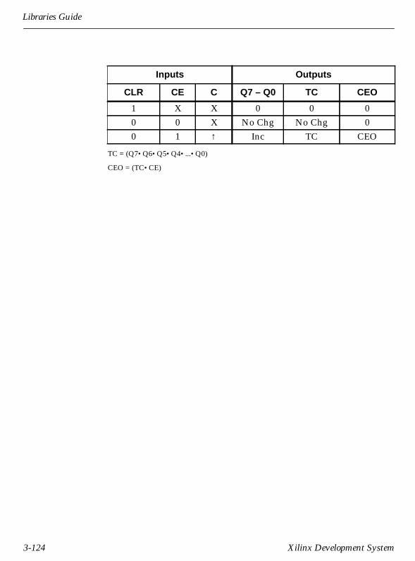
Libraries Guide
TC = (Q7•Q6•Q5•Q4•...•Q0)
CEO = (TC•CE)
Inputs Outputs
CLR CE C Q7 – Q0 TC CEO
1 X X 0 0 00 0 X No Chg No Chg 00 1 ↑ Inc TC CEO
3-124 Xilinx Development System
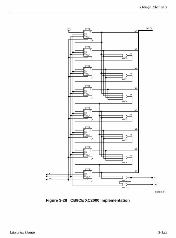
Design Elements
Figure 3-28 CB8CE XC2000 Implementation
CEO
AND2
AND2
TC
CE
AND3
AND2
AND4
T4
T3
AND3
AND2
AND4
T6
Q1
QT
CLR
CEC
FTCE
Q0
QT
CLR
CEC
FTCE
Q4
QT
CLR
CEC
FTCE
Q3
QT
CLR
CEC
FTCE
Q2
QT
CLR
CEC
FTCE
VCC
Q5
QT
CLR
CEC
FTCE
Q6
QT
CLR
CEC
FTCE
Q7
QT
CLR
CEC
FTCE
T2
C
CLR
T5
Q7
Q4
Q1
Q0Q[7:0]
Q2
Q3
Q5
Q6
T7
CB8CE.2K
Libraries Guide 3-125

Libraries Guide
Figure 3-29 CB8CE XC3000/XC4000 Implementation
CEO
TC
AND2
CE
T6
T5
T4
AND4
AND3
Q1
QT
CLRCEC
FTCE
Q0
QT
CLRCEC
FTCE
Q4
QT
CLRCEC
FTCE
Q3
QT
CLRCEC
FTCE
Q2
QT
CLRCEC
FTCE
VCC
AND4
AND3Q5
QT
CLRCEC
FTCE
Q6
QT
CLRCEC
FTCE
Q7
QT
CLRCEC
FTCE
AND2
AND5
T3
T2
T7
C
CLR
Q7
Q6
Q5
Q3
Q2
Q[7:0]Q0
Q1
Q4
AND2
CB8CE.3K, 4K
3-126 Xilinx Development System

Design Elements
CB8CLE
8-Bit Loadable Cascadable Binary Counter withClock Enable and Asynchronous Clear
CB8CLE is an 8-stage, 8-bit, synchronous, loadable, clearable, cascad-able binary counter. The asynchronous clear (CLR) is the highestpriority input. When CLR is High, all other inputs are ignored anddata (Q7 – Q0) and terminal count (TC) outputs go to logic level zero,independent of clock transitions. The data on the D7 – D0 inputs isloaded into the counter when the load enable input (L) is Highduring the Low-to-High clock (C) transition, independent of the stateof clock enable (CE). The outputs (Q7 – Q0) increment when CE isHigh during the Low-to-High clock transition. The counter ignoresclock transitions when CE is Low. The TC output is High when all Qoutputs are High.
Larger counters are created by connecting the count enable out (CEO)output of the first stage to the CE input of the next stage and byconnecting the C, L, and CLR inputs in parallel. CEO is active (High)when TC and CE are High. The maximum length of the counter isdetermined by the accumulated CE-to-TC propagation delays versusthe clock period. The clock period must be greater than n(tCE-TC),where “n” is the number of stages and “tCE-TC” is the CE-to-TCpropagation delay of each stage.
The counter is asynchronously reset, output Low, when power isapplied or when global reset (GR for XC2000, XC3000) or globalset/reset (GSR for XC4000) is active. GR is active-Low; the GSR activelevel is programmable. When cascading counters, use the CEOoutput if the counter uses the CE input; use the TC output if it doesnot.
XC2000 XC3000 XC4000 XC7000
Macro Macro Macro Primitive
Q[7:0]
X4362
CB8CLE
C
CLR
CE
TC
D[7:0]
LCEO
Libraries Guide 3-127

Libraries Guide
TC = (Q7•Q6•Q5•Q4•...•Q0)
CEO = (TC•CE)
dn = state of referenced input one set-up time prior to active clock transition
Inputs Outputs
CLR L CE C D7 – D0 Q7 – Q0 TC CEO
1 X X X X 0 0 00 1 X ↑ D d7 – d0 TC CEO0 0 0 X X No Chg No Chg 00 0 1 ↑ X Inc TC CEO
3-128 Xilinx Development System

Design Elements
Figure 3-30 CB8CLE XC2000 Implementation
CE
L
AND2
TC
AND2
CEO
T7
AND4
T6
AND3
AND2
T4
AND4
T3
AND3
AND2
C
CLR
T5
T2
D0
D2
D3
D6
D[7:0] D7
D5
D4
D1
Q6
CET
CLR
QLD
C
FTCLE
Q5
CET
CLR
QLD
C
FTCLE
VCC
Q4
CET
CLR
QLD
C
FTCLE
Q1
CET
CLR
QLD
C
FTCLE
Q0
CET
CLR
QLD
C
FTCLE
Q2
CET
CLR
QLD
C
FTCLE
Q3
CET
CLR
QLD
C
FTCLE
Q5
Q4
Q3
Q2
Q1
Q0
Q[7:0]
Q7
Q6
Q7
CET
CLR
QLD
C
FTCLE
CB8CLE.2K
Libraries Guide 3-129

Libraries Guide
Figure 3-31 CB8CLE XC3000/4000 Implementation
CE
AND2
Q6
Q4
Q3
Q2
Q1
Q0
Q[7:0]
Q7
Q5
C
CLR
T2
T3
D0
D2
D3
D6
D[7:0] D7
D5
D4
D1
Q6
CET
CLR
QLD
C
FTCLE
AND3Q5
CET
CLR
QLD
C
FTCLE
AND2
VCC
Q4
CET
CLR
QLD
C
FTCLE
Q1
CET
CLR
QLD
C
FTCLE
Q0
CET
CLR
QLD
C
FTCLE
Q2
CET
CLR
QLD
C
FTCLE
Q3
CET
CLR
QLD
C
FTCLE
AND3
AND4
AND4
Q7
CET
CLR
QLD
C
FTCLE
T4
T6
T5
T7
AND2
AND5
TC
CEO
L
CB8CLE.3K, 4K
3-130 Xilinx Development System

Design Elements
CB8CLED
8-Bit Loadable Cascadable Bidirectional BinaryCounter with Clock Enable and Asynchronous Clear
CB8CLED is an 8-stage, 8-bit, synchronous, loadable, clearable,cascadable, bidirectional binary counter. The asynchronous clear(CLR) is the highest priority input. When CLR is High, all otherinputs are ignored and data (Q7 – Q0) and terminal count (TC)outputs go to logic level zero, independent of clock transitions. Thedata on the D7 – D0 inputs is loaded into the counter when the loadenable input (L) is High during the Low-to-High clock (C) transition,independent of the state of CE. The outputs (Q7 – Q0) decrementwhen CE is High and UP is Low during the Low-to-High clock tran-sition. The outputs (Q7 – Q0) increment when CE and UP are High.The counter ignores clock transitions when CE is Low.
For counting up, the TC output is High when all Q outputs and UPare High. For counting down, the TC output is High when all Qoutputs and UP are Low. To cascade counters, the count enable out(CEO) output of each counter is connected to the CE pin of the nextstage. The clock, UP, L, and CLR inputs are connected in parallel.CEO is active (High) when TC and CE are High. The maximumlength of the counter is determined by the accumulated CE-to-TCpropagation delays versus the clock period. The clock period must begreater than n(tCE-TC), where “n” is the number of stages and“tCE-TC” is the CE-to-TC propagation delay of each stage. For EPLDdesigns, refer to “CB8X1” for high-performance cascadable, bidirec-tional counters.
The counter is asynchronously reset, output Low, when power isapplied or when global reset (GR for XC2000, XC3000) or globalset/reset (GSR for XC4000) is active. GR is active-Low; the GSR activelevel is programmable. When cascading counters, use the CEOoutput if the counter uses the CE input; use the TC output if it doesnot.
XC2000 XC3000 XC4000 XC7000
Macro Macro Macro Primitive
Q[7:0]
X4363
CB8CLED
C
CLR
CE
D[7:0]
L
UP
TC
CEO
Libraries Guide 3-131

Libraries Guide
TC = (Q7•Q6•Q5•...•Q0•UP) + (Q7•Q6•Q5•...•Q0•UP)
CEO = (TC•CE)
dn = state of referenced clock one set-up time prior to active clock transition
Inputs Outputs
CLR L CE C UP D7 – D0 Q7 – Q0 TC CEO
1 X X X X X 0 0 00 1 X ↑ X D d7 – d0 TC CEO0 0 0 X X X No Chg No Chg 00 0 1 ↑ 1 X Inc TC CEO0 0 1 ↑ 0 X Dec TC CEO
3-132 Xilinx Development System

Design Elements
Figure 3-32 CB8CLED XC2000 Implementation
CE
L
CEO
Q7
CET
CLR
QLD
C
FTCLE
C
CLR
D4
D5
D7
D6
D2
D1
D0
D[7:0]
D3
T7
T5_UP
T5_DN
T4
T4_UP
T4_DN
T2_DN
T2_UP
T1
T3_DN
T3_UP
T4
D0D1 O
S0
M2_1
T5
D0D1 O
S0
M2_1Q4
CET
CLR
QLD
C
FTCLE
Q0
CET
CLR
QLD
C
FTCLE
Q1
CET
CLR
QLD
C
FTCLE
T2
D0D1 O
S0
M2_1
VCC
T1
D0
S0
OD1
M2_1B1
T3
D0D1 O
S0
M2_1Q2
CET
CLR
QLD
C
FTCLE
Q5
CET
CLR
QLD
C
FTCLE
Q3
CET
CLR
QLD
C
FTCLE
Q6
CET
CLR
QLD
C
FTCLE
T6
T5
T6
D0D1 O
S0
M2_1T6_DN
T6_UP
T7_DN
T7_UP T7
D0D1 O
S0
M2_1
TC_DN
TC_UP TC
D0D1 O
S0
M2_1
AND2B2 T2
AND2
AND3B3
AND3
AND2B1
AND2
AND3B2
AND3
Q6
Q4
Q3
Q2
Q1
Q0
Q7 Q[7:0]
Q5
AND2B1
AND2
AND3B2
AND3
AND2B1
AND2UP
TC
T3
AND2CB8CLED.2K
Libraries Guide 3-133

Libraries Guide
Figure 3-33 CB8CLED XC3000 Implementation
CE
AND2
UP
Q7
Q4
Q3
Q2
Q1
Q0
Q5
Q6
Q[7:0]
T6
T7_DN
T7_UP
T7
TC_DN
TC_UP
D3
D[7:0]
D0
D1
D2
D6
D7
D5
D4
T5_UP
T5_DN
T4
T4_UP
T4_DN
T2_DN
T2_UP
T2
T1
T3_DN
T3_UP
T6_DN
T6_UP
T3
T5
CLRC
T4
D0D1 OS0
M2_1
Q6
CET
CLR
QLD
C
FTCLE
AND3
Q7
CET
CLR
QLD
C
FTCLE AND2
T7
D0D1 OS0
M2_1
T5
D0D1 OS0
M2_1
AND2
Q4
CET
CLR
QLD
C
FTCLE
Q0
CET
CLR
QLD
C
FTCLE
Q1
CET
CLR
QLD
C
FTCLE
AND2B2
T2
D0D1 OS0
M2_1
VCC
T1
D0
S0OD1
M2_1B1
T3
D0D1 OS0
M2_1Q2
CET
CLR
QLD
C
FTCLE
AND3B3
AND2
AND3
Q5
CET
CLR
QLD
C
FTCLE
T6
D0D1 OS0
M2_1
Q3
CET
CLR
QLD
C
FTCLE
AND4
AND3
AND2B1
AND3B2
AND4B3
AND2B1
AND3B2
TC
D0D1 OS0
M2_1
CEO
TC
L
CB8CLED.3K
3-134 Xilinx Development System

Design Elements
Figure 3-34 CB8CLED XC4000 Implementation
T2
AND2B1
T4
Q1
Q0
Q2
Q3
Q5
Q6
Q[7:0]
Q7
Q4
TC_UP
TC
C
L
CLR
CE
T2_DN
T2_UP
UP
T1
T4_UP
T4_DN
T3
T3_DN
T3_UP
T5_DN
T5_UP
T5
D7
D6
D5
D4
D3
D2
D1
D0
D[7:0]
T6_DN
T6
T7
T7_DN
T7_UP
TC_DN
AND5
Q0
CET
CLR
QLD
C
FTCLE
AND4
Q1
CET
CLR
QLD
C
FTCLE
AND2B2
T2
D0D1 O
S0
M2_1
VCC+5
T1
D0
S0
OD1
M2_1B1
AND3
T3
D0D1
O
S0
M2_1Q2
CET
CLR
QLD
C
FTCLE
Q3
CET
CLR
Q
LD
C
FTCLE
AND3B3
AND4B4
AND4
Q5
CET
CLR
QLD
C
FTCLE
AND2
AND3
AND2
Q7
CET
CLR
QLD
C
FTCLE
Q4
CET
CLR
QLD
C
FTCLE
Q6
CET
CLR
QLD
C
FTCLE
T6
D0D1
O
S0
M2_1
T7
D0D1
O
S0
M2_1
TC
D0D1
O
S0
M2_1
T5
D0D1
O
S0
M2_1
T4
D0D1 O
S0
M2_1
AND3B2
AND4B3
AND5B4
T6_UP
X4046
AND2
CEO
Libraries Guide 3-135
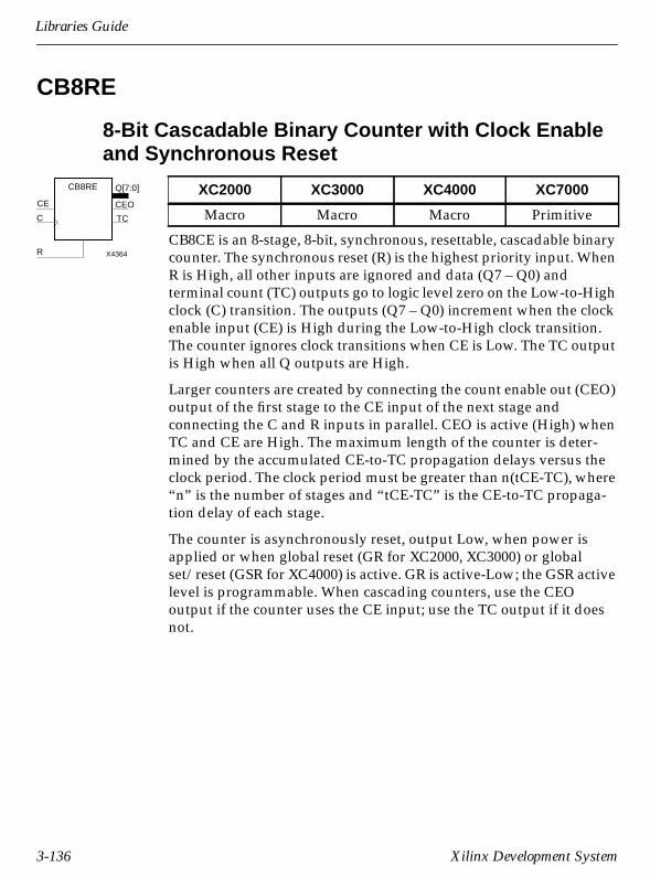
Libraries Guide
CB8RE
8-Bit Cascadable Binary Counter with Clock Enableand Synchronous Reset
CB8CE is an 8-stage, 8-bit, synchronous, resettable, cascadable binarycounter. The synchronous reset (R) is the highest priority input. WhenR is High, all other inputs are ignored and data (Q7 – Q0) andterminal count (TC) outputs go to logic level zero on the Low-to-Highclock (C) transition. The outputs (Q7 – Q0) increment when the clockenable input (CE) is High during the Low-to-High clock transition.The counter ignores clock transitions when CE is Low. The TC outputis High when all Q outputs are High.
Larger counters are created by connecting the count enable out (CEO)output of the first stage to the CE input of the next stage andconnecting the C and R inputs in parallel. CEO is active (High) whenTC and CE are High. The maximum length of the counter is deter-mined by the accumulated CE-to-TC propagation delays versus theclock period. The clock period must be greater than n(tCE-TC), where“n” is the number of stages and “tCE-TC” is the CE-to-TC propaga-tion delay of each stage.
The counter is asynchronously reset, output Low, when power isapplied or when global reset (GR for XC2000, XC3000) or globalset/reset (GSR for XC4000) is active. GR is active-Low; the GSR activelevel is programmable. When cascading counters, use the CEOoutput if the counter uses the CE input; use the TC output if it doesnot.
XC2000 XC3000 XC4000 XC7000
Macro Macro Macro Primitive
Q[7:0]
X4364
CB8RE
C
R
CE CEO
TC
3-136 Xilinx Development System

Design Elements
TC = (Q7•Q6•Q5•...•Q0)
CEO = (TC•CE)
Inputs Outputs
R CE C Q7 – Q0 TC CEO
1 X ↑ 0 0 00 0 X No Chg No Chg 00 1 ↑ Inc TC CEO
Libraries Guide 3-137

Libraries Guide
Figure 3-35 CB8RE XC2000 Implementation
GND CEOAND2
AND3
AND2
T4
AND4
AND2
AND3
T6
T5
AND4
T3
Q0
CCE
R
T S Q
FTRSE
Q1
CCE
R
T S Q
FTRSE
Q2
CCE
R
T S Q
FTRSE
Q3
CCE
R
T S Q
FTRSE
Q4
CCE
R
T S Q
FTRSE
Q5
CCE
R
T S Q
FTRSE
Q6
CCE
R
T S Q
FTRSE
VCC
Q7
CCE
R
T S Q
FTRSE
T2
C
R
Q6
Q4
Q3
Q2
Q0
Q1
Q5
Q[7:0]Q7
T7
AND2TC
CE
CB8RE.2K
3-138 Xilinx Development System

Design Elements
Figure 3-36 CB8RE XC3000/4000 Implementation
CEO
TC
AND2
CE
AND5
AND4
AND3
AND2
AND4
AND3
Q0
CCE
R
T S Q
FTRSE
Q1
CCE
R
T S Q
FTRSE
Q2
CCE
R
T S Q
FTRSE
Q3
CCE
R
T S Q
FTRSE
Q4
CCE
R
T S Q
FTRSE
Q5
CCE
R
T S Q
FTRSE
Q6
CCE
R
T S Q
FTRSE
VCC
GND
Q7
CCE
R
T S Q
FTRSEQ7
Q6
Q5
Q1
Q0
Q2
Q3
Q4
Q[7:0]
T4
T6
T5
T3
T2
C
R
T7
AND2
CB8RE.3K, 4K
Libraries Guide 3-139
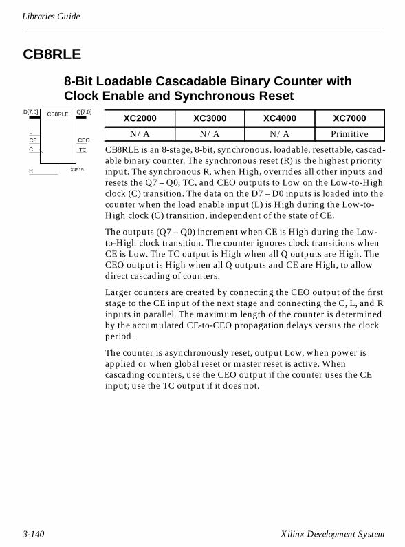
Libraries Guide
CB8RLE
8-Bit Loadable Cascadable Binary Counter withClock Enable and Synchronous Reset
CB8RLE is an 8-stage, 8-bit, synchronous, loadable, resettable, cascad-able binary counter. The synchronous reset (R) is the highest priorityinput. The synchronous R, when High, overrides all other inputs andresets the Q7 – Q0, TC, and CEO outputs to Low on the Low-to-Highclock (C) transition. The data on the D7 – D0 inputs is loaded into thecounter when the load enable input (L) is High during the Low-to-High clock (C) transition, independent of the state of CE.
The outputs (Q7 – Q0) increment when CE is High during the Low-to-High clock transition. The counter ignores clock transitions whenCE is Low. The TC output is High when all Q outputs are High. TheCEO output is High when all Q outputs and CE are High, to allowdirect cascading of counters.
Larger counters are created by connecting the CEO output of the firststage to the CE input of the next stage and connecting the C, L, and Rinputs in parallel. The maximum length of the counter is determinedby the accumulated CE-to-CEO propagation delays versus the clockperiod.
The counter is asynchronously reset, output Low, when power isapplied or when global reset or master reset is active. Whencascading counters, use the CEO output if the counter uses the CEinput; use the TC output if it does not.
XC2000 XC3000 XC4000 XC7000
N/A N/A N/A Primitive
Q[7:0]
X4515
CB8RLE
C
R
CE CEO
TC
D[7:0]
L
3-140 Xilinx Development System

Design Elements
TC = Q7•Q6•...•Q0
CEO = TC•CE
dn = state of referenced input one set-up time prior to active clock transition
Inputs Outputs
R L CE C D7 – D0 Q7 – Q0 TC CEO
1 X X ↑ X 0 0 00 1 X ↑ D d7 – d0 TC CEO0 0 0 X X No Chg No Chg 00 0 1 ↑ X Inc TC CEO
Libraries Guide 3-141

Libraries Guide
CB8X1
8-Bit Loadable Cascadable Bidirectional BinaryCounter with Clock Enable and Asynchronous Clear
CB8X1 is an 8-stage, 8-bit, synchronous, loadable, clearable, bidirec-tional binary counter. CB8X1 has separate count-enable inputs andsynchronous terminal-count outputs for up and down directions tosupport high-speed cascading in the EPLD architecture.
The asynchronous clear (CLR) is the highest priority input. WhenCLR is High, all other inputs are ignored, data outputs (Q7 – Q0) goto logic level zero, and terminal count outputs TCU and TCD go tozero and one, respectively, independent of clock transitions. The dataon the D7 – D0 inputs loads into the counter on the Low-to-Highclock (C) transition when the load enable input (L) is High, indepen-dent of the CE inputs.
The outputs (Q7 – Q0) increment when CEU is High, provided CLRand L are Low, during the Low-to-High clock transition. The outputs(Q7 – Q0) decrement when CED is High, provided CLR and L areLow. The counter ignores clock transitions when CEU and CED areLow. Both CEU and CED should not be High during the same clocktransition; the CEOU and CEOD outputs might not function properlyfor cascading when CEU and CED are both High.
For counting up, the CEOU output is High when all Q outputs andCEU are High. For counting down, the CEOD output is High whenall Q outputs are Low and CED is High. To cascade counters, theCEOU and CEOD outputs of each counter are connected directly tothe CEU and CED inputs, respectively, of the next stage. The C, L, andCLR inputs are connected in parallel.
In Xilinx EPLD devices, the maximum clocking frequency of thesecounter components is unaffected by the number of cascaded stagesfor all counting and loading functions. The TCU terminal countoutput is High when all Q outputs are High, regardless of CEU. TheTCD output is High when all Q outputs are Low, regardless of CED.When cascading counters, the final terminal count signals can be
XC2000 XC3000 XC4000 XC7000
N/A N/A N/A Primitive
X4198
CB8X1
C
Q[7:0]
CEU
L
CED
CLR
TCU
TCD
CEOU
CEOD
D[7:0]
3-142 Xilinx Development System
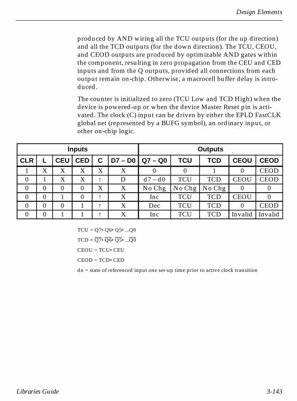
Design Elements
produced by AND wiring all the TCU outputs (for the up direction)and all the TCD outputs (for the down direction). The TCU, CEOU,and CEOD outputs are produced by optimizable AND gates withinthe component, resulting in zero propagation from the CEU and CEDinputs and from the Q outputs, provided all connections from eachoutput remain on-chip. Otherwise, a macrocell buffer delay is intro-duced.
The counter is initialized to zero (TCU Low and TCD High) when thedevice is powered-up or when the device Master Reset pin is acti-vated. The clock (C) input can be driven by either the EPLD FastCLKglobal net (represented by a BUFG symbol), an ordinary input, orother on-chip logic.
TCU = Q7•Q6•Q5•...Q0
TCD = Q7•Q6•Q5•...Q0
CEOU = TCU•CEU
CEOD = TCD•CED
dn = state of referenced input one set-up time prior to active clock transition
Inputs Outputs
CLR L CEU CED C D7 – D0 Q7 – Q0 TCU TCD CEOU CEOD
1 X X X X X 0 0 1 0 CEOD0 1 X X ↑ D d7 – d0 TCU TCD CEOU CEOD0 0 0 0 X X No Chg No Chg No Chg 0 00 0 1 0 ↑ X Inc TCU TCD CEOU 00 0 0 1 ↑ X Dec TCU TCD 0 CEOD0 0 1 1 ↑ X Inc TCU TCD Invalid Invalid
Libraries Guide 3-143
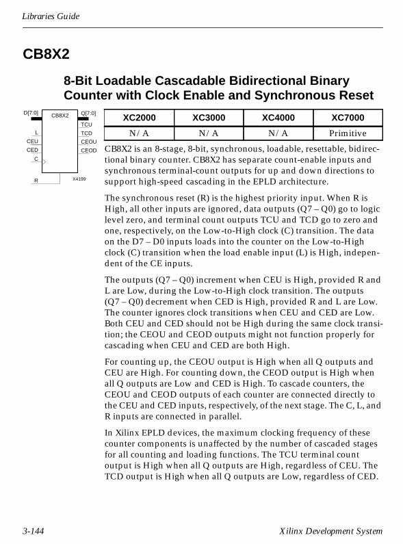
Libraries Guide
CB8X2
8-Bit Loadable Cascadable Bidirectional BinaryCounter with Clock Enable and Synchronous Reset
CB8X2 is an 8-stage, 8-bit, synchronous, loadable, resettable, bidirec-tional binary counter. CB8X2 has separate count-enable inputs andsynchronous terminal-count outputs for up and down directions tosupport high-speed cascading in the EPLD architecture.
The synchronous reset (R) is the highest priority input. When R isHigh, all other inputs are ignored, data outputs (Q7 – Q0) go to logiclevel zero, and terminal count outputs TCU and TCD go to zero andone, respectively, on the Low-to-High clock (C) transition. The dataon the D7 – D0 inputs loads into the counter on the Low-to-Highclock (C) transition when the load enable input (L) is High, indepen-dent of the CE inputs.
The outputs (Q7 – Q0) increment when CEU is High, provided R andL are Low, during the Low-to-High clock transition. The outputs(Q7 – Q0) decrement when CED is High, provided R and L are Low.The counter ignores clock transitions when CEU and CED are Low.Both CEU and CED should not be High during the same clock transi-tion; the CEOU and CEOD outputs might not function properly forcascading when CEU and CED are both High.
For counting up, the CEOU output is High when all Q outputs andCEU are High. For counting down, the CEOD output is High whenall Q outputs are Low and CED is High. To cascade counters, theCEOU and CEOD outputs of each counter are connected directly tothe CEU and CED inputs, respectively, of the next stage. The C, L, andR inputs are connected in parallel.
In Xilinx EPLD devices, the maximum clocking frequency of thesecounter components is unaffected by the number of cascaded stagesfor all counting and loading functions. The TCU terminal countoutput is High when all Q outputs are High, regardless of CEU. TheTCD output is High when all Q outputs are Low, regardless of CED.
XC2000 XC3000 XC4000 XC7000
N/A N/A N/A Primitive
X4199
CB8X2
C
Q[7:0]
CEU
L
CED
R
TCU
TCD
CEOU
CEOD
D[7:0]
3-144 Xilinx Development System

Design Elements
When cascading counters, the final terminal count signals can beproduced by AND wiring all the TCU outputs (for the up direction)and all the TCD outputs (for the down direction). The TCU, CEOU,and CEOD outputs are produced by optimizable AND-gates withinthe component, resulting in zero propagation from the CEU and CEDinputs and from the Q outputs, provided all connections from eachoutput remain on-chip. Otherwise, a macrocell buffer delay is intro-duced.
The counter is initialized to zero (TCU Low and TCD High) when thedevice is powered-up or when the device Master Reset pin is acti-vated. The clock (C) input can be driven by either the EPLD FastCLKglobal net (represented by a BUFG symbol), an ordinary input, orother on-chip logic.
TCU = Q7•Q6•Q5•...Q0
TCD = Q7•Q6•Q5•...Q0
CEOU = TCU•CEU
CEOD = TCD•CED
dn = state of referenced input one set-up time prior to active clock transition
Inputs Outputs
R L CEU CED C D7 – D0 Q7 – Q0 TCU TCD CEOU CEOD
1 X X X ↑ X 0 0 1 0 CEOD0 1 X X ↑ D d7 – d0 TCU TCD CEOU CEOD0 0 0 0 X X No Chg No Chg No Chg 0 00 0 1 0 ↑ X Inc TCU TCD CEOU 00 0 0 1 ↑ X Dec TCU TCD 0 CEOD0 0 1 1 ↑ X Inc TCU TCD Invalid Invalid
Libraries Guide 3-145

Libraries Guide
CB16CE
16-Bit Cascadable Binary Counter with Clock Enableand Asynchronous Clear
CB16CE is a 16-stage, 16-bit, synchronous, clearable, cascadablebinary counter. The asynchronous clear (CLR) is the highest priorityinput. When CLR is High, all other inputs are ignored and data(Q15 – Q0) and terminal count (TC) outputs go to logic level zero,independent of clock transitions. The outputs (Q15 – Q0) incrementwhen the clock enable input (CE) is High during the Low-to-Highclock (C) transition. The counter ignores clock transitions when CE isLow. The TC output is High when all Q outputs are High.
Larger counters are created by connecting the count enable out (CEO)output of the first stage to the CE input of the next stage andconnecting the C and CLR inputs in parallel. CEO is active (High)when TC is High and CE is High. The maximum length of the counteris determined by the accumulated CE-to-TC propagation delaysversus the clock period. The clock period must be greater than n(tCE-TC), where “n” is the number of stages and “tCE-TC” is the CE-to-TCpropagation delay of each stage.
The counter is asynchronously reset, output Low, when power isapplied or when global reset (GR for XC2000, XC3000) or globalset/reset (GSR for XC4000) is active. GR is active-Low; the GSR activelevel is programmable. When cascading counters, use the CEOoutput if the counter uses the CE input; use the TC output if it doesnot.
XC2000 XC3000 XC4000 XC7000
Macro Macro Macro Primitive
Q[15:0]
X4365
CB16CE
C
CLR
CEOCE
TC
3-146 Xilinx Development System

Design Elements
TC = (Q15•Q14•Q13•Q12...•Q0)
CEO = (TC•CE)
Inputs Outputs
CLR CE C Q15 – Q0 TC CEO
1 X X 0 0 00 0 X No Chg No Chg 00 1 ↑ Inc TC CEO
Libraries Guide 3-147

Libraries Guide
CB16CLE
16-Bit Loadable Cascadable Binary Counter withClock Enable and Asynchronous Clear
CB16CLE is a 16-stage, 16-bit, synchronous, loadable, clearable,cascadable binary counter. The asynchronous clear (CLR) is thehighest priority input. When CLR is High, all other inputs areignored and data (Q15 – Q0) and terminal count (TC) outputs go tologic level zero, independent of clock transitions. The data on theD15 – D0 inputs is loaded into the counter when the load enableinput (L) is High during the Low-to-High clock (C) transition, inde-pendent of the state of clock enable (CE). The outputs (Q15 – Q0)increment when CE is High during the Low-to-High clock transition.The counter ignores clock transitions when CE is Low. The TC outputis High when all Q outputs are High.
Larger counters are created by connecting the count enable out (CEO)output of the first stage to the CE input of the next stage andconnecting the C, L, and CLR inputs in parallel. CEO is active (High)when TC and CE are High. The maximum length of the counter isdetermined by the accumulated CE-to-TC propagation delays versusthe clock period. The clock period must be greater than n(tCE-TC),where “n” is the number of stages and “tCE-TC” is the CE-to-TCpropagation delay of each stage.
The counter is asynchronously reset, output Low, when power isapplied or when global reset (GR for XC2000, XC3000) or globalset/reset (GSR for XC4000) is active. GR is active-Low; the GSR activelevel is programmable. When cascading counters, use the CEOoutput if the counter uses the CE input; use the TC output if it doesnot.
XC2000 XC3000 XC4000 XC7000
Macro Macro Macro Primitive
Q[15:0]
X4366
CB16CLE
C
CLR
CE
TC
D[15:0]
L
CEO
3-148 Xilinx Development System

Design Elements
TC = (Q15•Q14•Q13•Q12...•Q0)
CEO = (TC•CE)
dn = state of referenced input one set-up time prior to active clock transition
Inputs Outputs
CLR L CE C D15 – D0 Q15 – Q0 TC CEO
1 X X X X 0 0 00 1 X ↑ D d15 – d0 TC CEO0 0 0 X X No Chg No Chg 00 0 1 ↑ X Inc TC CEO
Libraries Guide 3-149

Libraries Guide
CB16CLED
16-Bit Loadable Cascadable Bidirectional BinaryCounter with Clock Enable and Asynchronous Clear
CB16CLED is a 16-stage, 16-bit, synchronous, loadable, clearable,cascadable, bidirectional binary counter. The asynchronous clear(CLR) is the highest priority input. When CLR is High, all otherinputs are ignored and data (Q15 – Q0) and terminal count (TC)outputs go to logic level zero, independent of clock transitions. Thedata on the D15 – D0 inputs is loaded into the counter when the loadenable input (L) is High during the Low-to-High clock (C) transition,independent of the state of clock enable (CE). The outputs (Q15 – Q0)decrement when CE is High and UP is Low during the Low-to-Highclock transition. The outputs (Q15 – Q0) increment when CE and UPare High. The counter ignores clock transitions when CE is Low.
For counting up, the TC output is High when all Q outputs and UPare High. For counting down, the TC output is High when all Qoutputs and UP are Low. To cascade counters, the count enable out(CEO) output of each counter is connected to the CE pin of the nextstage. The clock, UP, L, and CLR inputs are connected in parallel.CEO is active (High) when TC and CE are High. The maximumlength of the counter is determined by the accumulated CE-to-TCpropagation delays versus the clock period. The clock period must begreater than n(tCE-TC), where “n” is the number of stages and“tCE-TC” is the CE-to-TC propagation delay of each stage. For EPLDdesigns, refer to “CB16X1” for high-performance cascadable, bidirec-tional counters.
The counter is asynchronously reset, output Low, when power isapplied or when global reset (GR for XC2000, XC3000) or globalset/reset (GSR for XC4000) is active. GR is active-Low; the GSR activelevel is programmable. When cascading counters, use the CEOoutput if the counter uses the CE input; use the TC output if it doesnot.
XC2000 XC3000 XC4000 XC7000
Macro Macro Macro Primitive
Q[15:0]
X4367
CB16CLED
C
CLR
CE
D[15:0]
L
UP
TC
CEO
3-150 Xilinx Development System

Design Elements
TC = (Q15•Q14•Q13...•Q0•UP) + (Q15•Q14•Q13...•Q0•UP)
CEO = (TC•CE)
dn = state of referenced clock one set-up time prior to active clock transition
Inputs Outputs
CLR L CE C UP D15 – D0 Q15 – Q0 TC CEO
1 X X X X X 0 0 00 1 X ↑ X D d15 – d0 TC CEO0 0 0 X X X No Chg No Chg 00 0 1 ↑ 1 X Inc TC CEO0 0 1 ↑ 0 X Dec TC CEO
Libraries Guide 3-151
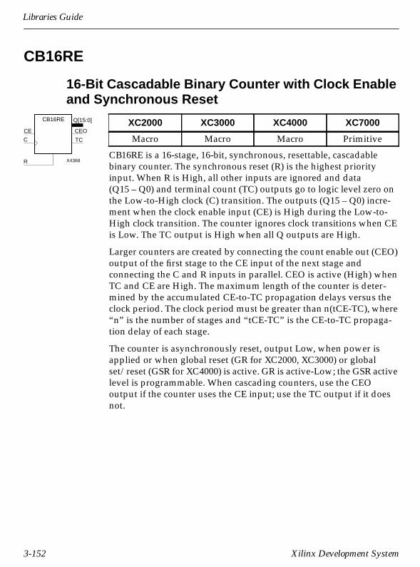
Libraries Guide
CB16RE
16-Bit Cascadable Binary Counter with Clock Enableand Synchronous Reset
CB16RE is a 16-stage, 16-bit, synchronous, resettable, cascadablebinary counter. The synchronous reset (R) is the highest priorityinput. When R is High, all other inputs are ignored and data(Q15 – Q0) and terminal count (TC) outputs go to logic level zero onthe Low-to-High clock (C) transition. The outputs (Q15 – Q0) incre-ment when the clock enable input (CE) is High during the Low-to-High clock transition. The counter ignores clock transitions when CEis Low. The TC output is High when all Q outputs are High.
Larger counters are created by connecting the count enable out (CEO)output of the first stage to the CE input of the next stage andconnecting the C and R inputs in parallel. CEO is active (High) whenTC and CE are High. The maximum length of the counter is deter-mined by the accumulated CE-to-TC propagation delays versus theclock period. The clock period must be greater than n(tCE-TC), where“n” is the number of stages and “tCE-TC” is the CE-to-TC propaga-tion delay of each stage.
The counter is asynchronously reset, output Low, when power isapplied or when global reset (GR for XC2000, XC3000) or globalset/reset (GSR for XC4000) is active. GR is active-Low; the GSR activelevel is programmable. When cascading counters, use the CEOoutput if the counter uses the CE input; use the TC output if it doesnot.
XC2000 XC3000 XC4000 XC7000
Macro Macro Macro Primitive
Q[15:0]
X4368
CB16RE
C
R
CEOCE
TC
3-152 Xilinx Development System

Design Elements
TC = (Q15•Q14•Q13...•Q0)
CEO = (TC•CE)
Inputs Outputs
R CE C Q15 – Q0 TC CEO
1 X ↑ 0 0 00 0 X No Chg No Chg 00 1 ↑ Inc TC CEO
Libraries Guide 3-153
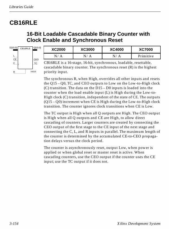
Libraries Guide
CB16RLE
16-Bit Loadable Cascadable Binary Counter withClock Enable and Synchronous Reset
CB16RLE is a 16-stage, 16-bit, synchronous, loadable, resettable,cascadable binary counter. The synchronous reset (R) is the highestpriority input.
The synchronous R, when High, overrides all other inputs and resetsthe Q15 – Q0, TC, and CEO outputs to Low on the Low-to-High clock(C) transition. The data on the D15 – D0 inputs is loaded into thecounter when the load enable input (L) is High during the Low-to-High clock (C) transition, independent of the state of CE. The outputs(Q15 – Q0) increment when CE is High during the Low-to-High clocktransition. The counter ignores clock transitions when CE is Low.
The TC output is High when all Q outputs are High. The CEO outputis High when all Q outputs and CE are High, to allow directcascading of counters. Larger counters are created by connecting theCEO output of the first stage to the CE input of the next stage andconnecting the C, L, and R inputs in parallel. The maximum length ofthe counter is determined by the accumulated CE-to-CEO propaga-tion delays versus the clock period.
The counter is asynchronously reset, output Low, when power isapplied or when global reset or master reset is active. Whencascading counters, use the CEO output if the counter uses the CEinput; use the TC output if it does not.
XC2000 XC3000 XC4000 XC7000
N/A N/A N/A Primitive
Q[15:0]
X4516
CB16RLE
C
R
CE CEO
TC
D[15:0]
L
3-154 Xilinx Development System

Design Elements
TC = Q15•Q14•...•Q0
CEO = TC•CE
dn = state of referenced input one set-up time prior to clock transition
Inputs Outputs
R L CE C D15 – D0 Q15 – Q0 TC CEO
1 X X ↑ X 0 0 00 1 X ↑ D d15 – d0 TC CEO0 0 0 X X No Chg No Chg 00 0 1 ↑ X Inc TC CEO
Libraries Guide 3-155

Libraries Guide
CB16X1
16-Bit Loadable Cascadable Bidirectional BinaryCounter with Clock Enable and Asynchronous Clear
CB16X1 is a 16-stage, 16-bit, synchronous, loadable, clearable, bidirec-tional binary counter. CB16X1 has separate count-enable inputs andsynchronous terminal-count outputs for up and down directions tosupport high-speed cascading in the EPLD architecture.
The asynchronous clear (CLR) is the highest priority input. WhenCLR is High, all other inputs are ignored, data outputs (Q15 – Q0) goto logic level zero, and terminal count outputs TCU and TCD go tozero and one, respectively, independent of clock transitions. The dataon the D15 – D0 inputs loads into the counter on the Low-to-Highclock (C) transition, when the load enable input (L) is High, indepen-dent of the CE inputs.
The outputs (Q15 – Q0) increment when CEU is High, provided CLRand L are Low, during the Low-to-High clock transition. The outputs(Q15 – Q0) decrement when CED is High, provided CLR and L areLow. The counter ignores clock transitions when CEU and CED areLow. Both CEU and CED should not be High during the same clocktransition; the CEOU and CEOD outputs might not function properlyfor cascading when CEU and CED are both High.
For counting up, the CEOU output is High when all Q outputs andCEU are High. For counting down, the CEOD output is High whenall Q outputs are Low and CED is High. To cascade counters, theCEOU and CEOD outputs of each counter are connected directly tothe CEU and CED inputs, respectively, of the next stage. The clock, L,and CLR inputs are connected in parallel.
In Xilinx EPLD devices, the maximum clocking frequency of thesecounter components is unaffected by the number of cascaded stagesfor all counting and loading functions. The TCU terminal countoutput is High when all Q outputs are High, regardless of CEU. TheTCD output is High when all Q outputs are Low, regardless of CED.
XC2000 XC3000 XC4000 XC7000
N/A N/A N/A Primitive
X4200
CB16X1
C
Q[15:0]
CEU
L
CED
CLR
TCU
TCD
CEOU
CEOD
D[15:0]
3-156 Xilinx Development System

Design Elements
When cascading counters, the final terminal count signals can beproduced by AND wiring all the TCU outputs (for the up direction)and all the TCD outputs (for the down direction). The TCU, CEOU,and CEOD outputs are produced by optimizable AND gates withinthe component, resulting in zero propagation from the CEU and CEDinputs and from the Q outputs, provided all connections from eachoutput remain on-chip. Otherwise, a macrocell buffer delay is intro-duced. The counter is initialized to zero (TCU Low and TCD High)when the device is powered-up or when the device Master Reset pinis activated. The clock (C) input can be driven by either the EPLDFastCLK global net (represented by a BUFG symbol), an ordinaryinput, or other on-chip logic.
TCU = Q15•Q14•Q13•...•Q0
TCD = Q15•Q14•Q13•...•Q0
CEOU = TCU•CEU
CEOD = TCD•CED
dn = state of referenced input one set-up time prior to active clock transition
Inputs Outputs
CLR L CEU CED C D15 – D0 Q15 – Q0 TCU TCD CEOU CEOD
1 X X X X X 0 0 1 0 CEOD0 1 X X ↑ D d15 – d0 TCU TCD CEOU CEOD0 0 0 0 X X No Chg No Chg No Chg 0 00 0 1 0 ↑ X Inc TCU TCD CEOU 00 0 0 1 ↑ X Dec TCU TCD 0 CEOD0 0 1 1 ↑ X Inc TCU TCD Invalid Invalid
Libraries Guide 3-157

Libraries Guide
CB16X2
16-Bit Loadable Cascadable Bidirectional BinaryCounter with Clock Enable and Synchronous Reset
CB16X2 is a 16-stage, 16-bit, synchronous, loadable, resettable, bidi-rectional binary counter. CB16X2 has separate count-enable inputsand synchronous terminal-count outputs for up and down directions,to support high-speed cascading in the EPLD architecture.
The synchronous reset (R) is the highest priority input. When R isHigh, all other inputs are ignored, data outputs (Q15 – Q0) go to logiclevel zero, and terminal count outputs TCU and TCD go to zero andone, respectively, on the Low-to-High clock (C) transition. The dataon the D15 – D0 inputs loads into the counter on the Low-to-Highclock (C) transition when the load enable input (L) is High, indepen-dent of the CE inputs. The outputs (Q15 – Q0) increment when CEUis High, provided R and L are Low, during the Low-to-High clocktransition. The outputs (Q15 – Q0) decrement when CED is High,provided R and L are Low.
The counter ignores clock transitions when CEU and CED are Low.Both CEU and CED should not be High during the same clock transi-tion; the CEOU and CEOD outputs might not function properly forcascading when CEU and CED are both High. For counting up, theCEOU output is High when all Q outputs and CEU are High. Forcounting down, the CEOD output is High when all Q outputs areLow and CED is High. To cascade counters, the CEOU and CEODoutputs of each counter are connected directly to the CEU and CEDinputs, respectively, of the next stage. The C, L, and R inputs areconnected in parallel.
In Xilinx EPLD devices, the maximum clocking frequency of thesecounter components is unaffected by the number of cascaded stagesfor all counting and loading functions. The TCU terminal countoutput is High when all Q outputs are High, regardless of CEU. TheTCD output is High when all Q outputs are Low, regardless of CED.
XC2000 XC3000 XC4000 XC7000
N/A N/A N/A Primitive
X4201
CB16X2
C
Q[15:0]
CEU
L
CED
R
TCU
TCD
CEOU
CEOD
D[15:0]
3-158 Xilinx Development System
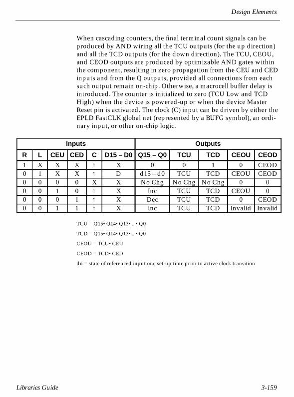
Design Elements
When cascading counters, the final terminal count signals can beproduced by AND wiring all the TCU outputs (for the up direction)and all the TCD outputs (for the down direction). The TCU, CEOU,and CEOD outputs are produced by optimizable AND gates withinthe component, resulting in zero propagation from the CEU and CEDinputs and from the Q outputs, provided all connections from eachsuch output remain on-chip. Otherwise, a macrocell buffer delay isintroduced. The counter is initialized to zero (TCU Low and TCDHigh) when the device is powered-up or when the device MasterReset pin is activated. The clock (C) input can be driven by either theEPLD FastCLK global net (represented by a BUFG symbol), an ordi-nary input, or other on-chip logic.
TCU = Q15•Q14•Q13•...•Q0
TCD = Q15•Q14•Q13•...•Q0
CEOU = TCU•CEU
CEOD = TCD•CED
dn = state of referenced input one set-up time prior to active clock transition
Inputs Outputs
R L CEU CED C D15 – D0 Q15 – Q0 TCU TCD CEOU CEOD
1 X X X ↑ X 0 0 1 0 CEOD0 1 X X ↑ D d15 – d0 TCU TCD CEOU CEOD0 0 0 0 X X No Chg No Chg No Chg 0 00 0 1 0 ↑ X Inc TCU TCD CEOU 00 0 0 1 ↑ X Dec TCU TCD 0 CEOD0 0 1 1 ↑ X Inc TCU TCD Invalid Invalid
Libraries Guide 3-159

Libraries Guide
CC8CE
8-Bit Cascadable Binary Counter with Clock Enableand Asynchronous Clear
CC8CE is an 8-stage, 8-bit, synchronous, clearable, cascadable binarycounter. The counter is implemented using carry logic with relativelocation restraints, which assures most efficient logic placement. Theasynchronous clear (CLR) is the highest priority input. When CLR isHigh, all other inputs are ignored and data (Q7 – Q0) and terminalcount (TC) outputs go to logic level zero, independent of clock transi-tions. The outputs (Q7 – Q0) increment when the clock enable input(CE) is High during the Low-to-High clock (C) transition. Thecounter ignores clock transitions when CE is Low. The TC output isHigh when all Q outputs are High.
Larger counters are created by connecting the count enable out (CEO)output of the first stage to the CE input of the next stage andconnecting the C and CLR inputs in parallel. CEO is active (High)when TC and CE are High. The maximum length of the counter isdetermined by the accumulated CE-to-TC propagation delays versusthe clock period. The clock period must be greater than n(tCE-TC),where “n” is the number of stages and “tCE-TC” is the CE-to-TCpropagation delay of each stage.
The counter is asynchronously reset, output Low, when power isapplied or when global set/reset (GSR) is active. The GSR active levelis programmable. When cascading counters, use the CEO output ifthe counter uses the CE input; use the TC output if it does not.
XC2000 XC3000 XC4000 XC7000
N/A N/A Macro N/A
Q[7:0]
X4290
CC8CE
C
CLR
CE CEO
TC
3-160 Xilinx Development System
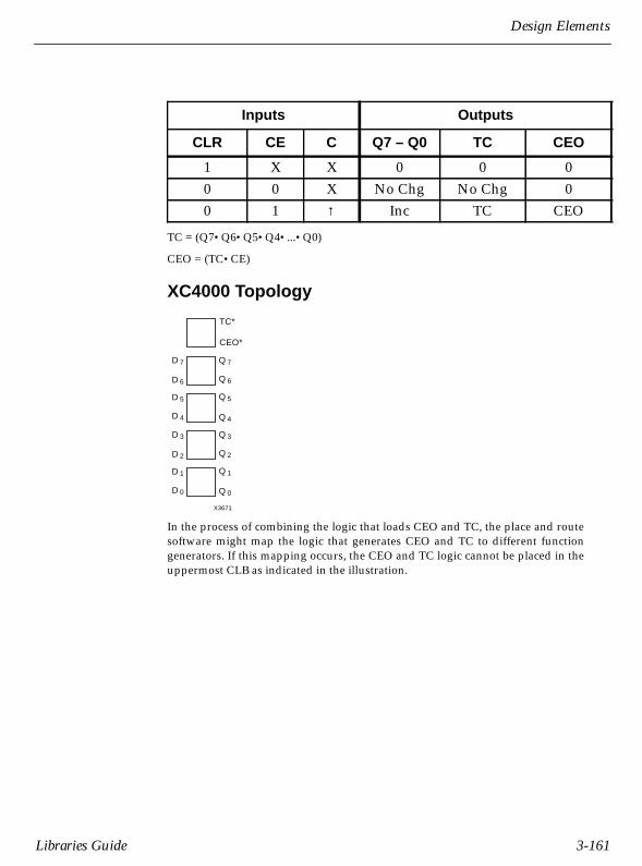
Design Elements
TC = (Q7•Q6•Q5•Q4•...•Q0)
CEO = (TC•CE)
XC4000 Topology
In the process of combining the logic that loads CEO and TC, the place and routesoftware might map the logic that generates CEO and TC to different functiongenerators. If this mapping occurs, the CEO and TC logic cannot be placed in theuppermost CLB as indicated in the illustration.
Inputs Outputs
CLR CE C Q7 – Q0 TC CEO
1 X X 0 0 00 0 X No Chg No Chg 00 1 ↑ Inc TC CEO
X3671
TC*
CEO*
Q 7
Q 6
Q 5
Q 4
D 7
D 6
D 5
D 4
Q 3
Q 2
Q 1
Q 0
D 3
D 2
D 1
D 0
Libraries Guide 3-161

Libraries Guide
Figure 3-37 CC8CE XC4000 Implementation
Q0
C1
Q2
Q3
Q5
Q[7:0]
Q7
Q6
Q4
Q1
Q0
CY4_19
INC-FG-1
CEO
AND2
TQ5
TQ0
TQ5
TQ4
TQ3
TQ2
TQ1
TQ7
C4
C3
C0
Q7
Q1
Q2
Q3
Q4
Q5
C1
C2
C3
C4
C5
C6
TQ1
TQ3
C2
C0
C5
Q6
TQ2
TQ7
TQ6
TQ6
TQ0
TQ4
CY4_18INC-FG-CI
CY4_18
INC-FG-CI
CY4_18
INC-FG-CI
XOR2
XOR2
XOR2
XOR2
XOR2
XOR2
XOR2
RLOC=R4C0.G
I1I2I3I4
O
FMAP
RLOC=R3C0.F
I1I2I3I4
O
FMAP
RLOC=R3C0.G
I1I2I3I4
O
FMAP
RLOC=R2C0.F
I1I2I3I4
O
FMAP
RLOC=R2C0.G
I1I2I3I4
O
FMAP
RLOC=R1C0.F
I1I2I3I4
O
FMAP
RLOC=R0C0
A0ADD
B1A1B0
CY4
CIN
COUT
COUT0
(F3)(F1)(F2)(G4)(G1)
CARRY MODE
CY4_42EXAMINE-CI
RLOC=R2C0
A0ADD
B1A1B0
CY4
CIN
COUT
COUT0
(F3)(F1)(F2)(G4)(G1)
CARRY MODE
RLOC=R1C0
A0ADD
B1A1B0
CY4
CIN
COUT
COUT0
(F3)(F1)(F2)(G4)(G1)
CARRY MODE
RLOC=R3C0
A0ADD
B1A1B0
CY4
CIN
COUT
COUT0
(F3)(F1)(F2)(G4)(G1)
CARRY MODE
RLOC=R1C0.G
I1I2I3I4
O
FMAP
RLOC=R4C0.F
I1I2I3I4
O
FMAP
Q0RLOC=R4C0.FFX
FDCE
QD
CLR
CEC
Q1RLOC=R4C0.FFY
FDCE
QD
CLR
CEC
Q2
RLOC=R3C0.FFX
FDCE
QD
CLR
CEC
Q3RLOC=R3C0.FFY
FDCE
QD
CLR
CEC
Q4
RLOC=R2C0.FFX
FDCE
QD
CLR
CEC
Q5RLOC=R2C0.FFY
FDCE
QD
CLR
CEC
Q6
RLOC=R1C0.FFX
FDCE
QD
CLR
CEC
Q7RLOC=R1C0.FFY
FDCE
QD
CLR
CEC
C6
TC
INV
RLOC=R4C0
A0ADD
B1A1B0
CY4
CIN
COUT
COUT0
(F3)(F1)(F2)(G4)(G1)
CARRY MODE
CEC
CLR
CC8CE.4K
3-162 Xilinx Development System
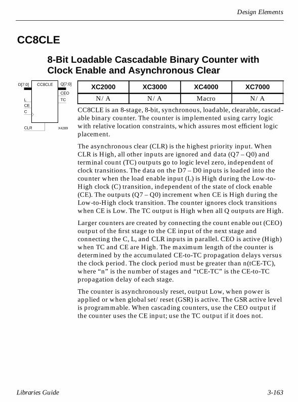
Design Elements
CC8CLE
8-Bit Loadable Cascadable Binary Counter withClock Enable and Asynchronous Clear
CC8CLE is an 8-stage, 8-bit, synchronous, loadable, clearable, cascad-able binary counter. The counter is implemented using carry logicwith relative location constraints, which assures most efficient logicplacement.
The asynchronous clear (CLR) is the highest priority input. WhenCLR is High, all other inputs are ignored and data (Q7 – Q0) andterminal count (TC) outputs go to logic level zero, independent ofclock transitions. The data on the D7 – D0 inputs is loaded into thecounter when the load enable input (L) is High during the Low-to-High clock (C) transition, independent of the state of clock enable(CE). The outputs (Q7 – Q0) increment when CE is High during theLow-to-High clock transition. The counter ignores clock transitionswhen CE is Low. The TC output is High when all Q outputs are High.
Larger counters are created by connecting the count enable out (CEO)output of the first stage to the CE input of the next stage andconnecting the C, L, and CLR inputs in parallel. CEO is active (High)when TC and CE are High. The maximum length of the counter isdetermined by the accumulated CE-to-TC propagation delays versusthe clock period. The clock period must be greater than n(tCE-TC),where “n” is the number of stages and “tCE-TC” is the CE-to-TCpropagation delay of each stage.
The counter is asynchronously reset, output Low, when power isapplied or when global set/reset (GSR) is active. The GSR active levelis programmable. When cascading counters, use the CEO output ifthe counter uses the CE input; use the TC output if it does not.
XC2000 XC3000 XC4000 XC7000
N/A N/A Macro N/A
Q[7:0]
X4289
CC8CLE
C
CLR
CE
D[7:0]
L
CEO
TC
Libraries Guide 3-163
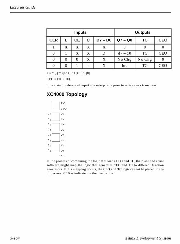
Libraries Guide
TC = (Q7•Q6•Q5•Q4•...•Q0)
CEO = (TC•CE)
dn = state of referenced input one set-up time prior to active clock transition
XC4000 Topology
In the process of combining the logic that loads CEO and TC, the place and routesoftware might map the logic that generates CEO and TC to different functiongenerators. If this mapping occurs, the CEO and TC logic cannot be placed in theuppermost CLB as indicated in the illustration.
Inputs Outputs
CLR L CE C D7 – D0 Q7 – Q0 TC CEO
1 X X X X 0 0 00 1 X X D d7 – d0 TC CEO0 0 0 X X No Chg No Chg 00 0 1 ↑ X Inc TC CEO
X3673
TC*
CEO*
Q 7
Q 6
Q 5
Q 4
D 7
D 6
D 5
D 4
Q 3
Q 2
Q 1
Q 0
D 3
D 2
D 1
D 0
3-164 Xilinx Development System

Design Elements
Figure 3-38 CC8CLE XC4000 Implementation
L
D0D[7:0]
D6
D1
D3
D7
D5
D2
D4
Q2
Q3
Q5
Q[7:0]
Q7
Q6
Q4
Q1
Q0
CE
MD0
CY4_19
INC-FG-1
AND2
RLOC=R0C0
A0ADD
B1A1B0
CY4
CIN
COUT
COUT0
(F3)(F1)(F2)(G4)(G1)
CARRY MODE
Q1RLOC=R4C0.FFY
FDCE
QD
CLR
CEC
Q0L
L
L
L
L
L
MD7
MD1
MD2
MD3
MD4
MD5
MD6
C4
C3
C0
D7
D1
D2
D3
D4
D5
C1
C2
C3
C4
C5
C6
D0
MD1
MD3
MD0
C1
C2
C0
C6
D6
TQ7
TQ6
TQ5
TQ4
TQ3
TQ2
TQ1
TQ0
MD5
MD2
MD7
MD6
LQ7
LQ6
Q1
Q2
Q3
Q4
Q5
MD4
XOR2
XOR2
XOR2
XOR2
XOR2
XOR2
XOR2
RLOC=R4C0.G
I1I2I3I4
O
FMAP
RLOC=R3C0.F
I1I2I3I4
O
FMAP
RLOC=R3C0.G
I1I2I3I4
O
FMAP
RLOC=R2C0.F
I1I2I3I4
O
FMAP
RLOC=R2C0.G
I1I2I3I4
O
FMAP
RLOC=R1C0.F
I1I2I3I4
O
FMAP
CY4_42EXAMINE-CI
CY4_18INC-FG-CI
CY4_18INC-FG-CI
RLOC=R2C0
A0ADD
B1A1B0
CY4
CIN
COUT
COUT0
(F3)(F1)(F2)(G4)(G1)
CARRY MODE
CY4_18INC-FG-CI
RLOC=R1C0
A0ADD
B1A1B0
CY4
CIN
COUT
COUT0
(F3)(F1)(F2)(G4)(G1)
CARRY MODE
RLOC=R4C0
A0ADD
B1A1B0
CY4
CIN
COUT
COUT0
(F3)(F1)(F2)(G4)(G1)
CARRY MODE
RLOC=R3C0
A0ADD
B1A1B0
CY4
CIN
COUT
COUT0
(F3)(F1)(F2)(G4)(G1)
CARRY MODE
RLOC=R1C0.G
I1I2I3I4
O
FMAP
RLOC=R4C0.F
I1I2I3I4
O
FMAP
Q2
RLOC=R3C0.FFX
FDCE
QD
CLR
CEC
Q3RLOC=R3C0.FFY
FDCE
QD
CLR
CEC
Q4
RLOC=R2C0.FFX
FDCE
QD
CLR
CEC
Q5RLOC=R2C0.FFY
FDCE
QD
CLR
CEC
Q6
RLOC=R1C0.FFX
FDCE
QD
CLR
CEC
Q7RLOC=R1C0.FFY
FDCE
QD
CLR
CEC
MD7
D0D1
O
S0
M2_1
MD6
D0D1
O
S0
M2_1
MD5
D0D1
O
S0
M2_1
MD4
D0D1
O
S0
M2_1
MD3
D0D1
O
S0
M2_1
MD2
D0D1
O
S0
M2_1
MD1
D0D1
O
S0
M2_1
MD0
D0D1
O
S0
M2_1
C5
TC
CEO
INV
Q0RLOC=R4C0.FFX
FDCE
QD
CLR
CECOR2
L_CE
CLRC
CC8CLE.4K
Libraries Guide 3-165

Libraries Guide
CC8CLED
8-Bit Loadable Cascadable Bidirectional BinaryCounter with Clock Enable and Asynchronous Clear
CC8CLED is an 8-stage, 8-bit, synchronous, loadable, clearable,cascadable, bidirectional binary counter. The counter is implementedusing carry logic with relative location constraints, which assuresmost efficient logic placement.
The asynchronous clear (CLR) is the highest priority input. WhenCLR is High, all other inputs are ignored and data (Q7 – Q0) andterminal count (TC) outputs go to logic level zero, independent ofclock transitions. The data on the D7 – D0 inputs is loaded into thecounter when the load enable input (L) is High during the Low-to-High clock (C) transition, independent of the state of clock enable(CE). The outputs (Q7 – Q0) decrement when CE is High and UP isLow during the Low-to-High clock transition. The outputs (Q7 – Q0)increment when CE and UP are High. The counter ignores clock tran-sitions when CE is Low.
For counting up, the TC output is High when all Q outputs and UPare High. For counting down, the TC output is High when all Qoutputs and UP are Low. To cascade counters, the count enable out(CEO) output of each counter is connected to the CE pin of the nextstage. The clock, UP, L, and CLR inputs are connected in parallel.CEO is active (High) when TC and CE are High. The maximumlength of the counter is determined by the accumulated CE-to-TCpropagation delays versus the clock period. The clock period must begreater than n(tCE-TC), where “n” is the number of stages and“tCE-TC” is the CE-to-TC propagation delay of each stage.
The counter is asynchronously reset, output Low, when power isapplied or when global set/reset (GSR) is active. The GSR active levelis programmable. When cascading counters, use the CEO output ifthe counter uses the CE input; use the TC output if it does not.
XC2000 XC3000 XC4000 XC7000
N/A N/A Macro N/A
Q[7:0]
X4287
CC8CLED
C
CLR
CE
D[7:0]
L
UP
CEO
TC
3-166 Xilinx Development System

Design Elements
TC = (Q7•Q6•Q5•...•Q0•UP) + (Q7•Q6•Q5•...•Q0•UP)
CEO = (TC•CE)
dn = state of referenced clock one set-up time prior to active clock transition
XC4000 Topology
In the process of combining the logic that loads CEO and TC, the place and routesoftware might map the logic that generates CEO and TC to different functiongenerators. If this mapping occurs, the CEO and TC logic cannot be placed in theuppermost CLB as indicated in the illustration.
Inputs Outputs
CLR L CE C UP D7 – D0 Q7 – Q0 TC CEO
1 X X X X X 0 0 00 1 X X X D d7 – d0 TC CEO0 0 0 X X X No Chg No Chg 00 0 1 ↑ 1 X Inc TC CEO0 0 1 ↑ 0 X Dec TC CEO
X4339
D 7
D 6
D 5
D 4
TC*
CEO*
Q 7
Q 6
Q 5
Q 4
Q 3
Q 2
Q 1
Q 0
D 3
D 2
D 1
D 0
Libraries Guide 3-167

Libraries Guide
LCE
C
UP
D0Q0
L
MD2_UP
MD2_UP
MD4_UP
MD5_UP
MD6_UP
D7Q7
L
MD6_UP
D[7:0]
D0
D1
D2
D3
D4
D5
D6
D7
TQ6_UP
C4_UP
C3_UP
C2_UP
C1_UP
C0_UP
C6_UP
MD4_UP
MD0_UP
MD3_UP
MD1_UP
TQ5_UP
TQ4_UP
TQ3_UP
TQ2_UP
TQ1_UP
TQ0_UP
C0_UPD1Q1
L
LQ2
C1_UP
C2_UPD3Q3
L
C3_UPD4Q4
L
LQ5
C4_UP
LQ6D6
C5_UP
TQ7_UPC6_UP
C5_UP
MD7_UP
MD0_UP
MD1_UP
MD3_UP
CO_UP CO_DN
D5
D2
MD5_UP
RLOC=R1C0.G
I1I2I3I4
O
FMAP
RLOC=R1C0.F
I1I2I3I4
O
FMAP
XOR2
MD6_UP
D0D1
O
S0
M2_1
CY4_19INC-FG-1
RLOC=R3C0
A0ADD
B1A1B0
CY4
CIN
COUT
COUT0
(F3)(F1)(F2)(G4)(G1)
CARRY MODE
RLOC=R4C0
A0ADD
B1A1B0
CY4
CIN
COUT
COUT0
(F3)(F1)(F2)(G4)(G1)
RLOC=R1C0
A0ADD
B1A1B0
CY4
CIN
COUT
COUT0
(F3)(F1)(F2)(G4)(G1)
CARRY MODE
CY4_18INC-FG-CI
RLOC=R2C0
A0ADD
B1A1B0
CY4
CIN
COUT
COUT0
(F3)(F1)(F2)(G4)(G1)
CARRY MODE
CY4_18INC-FG-CI
CY4_18INC-FG-CI
CY4_42EXAMINE-CI
RLOC=R0C0
A0ADD
B1A1B0
CY4
CIN
COUT
COUT0
(F3)(F1)(F2)(G4)(G1)
CARRY MODE
RLOC=R4C1
A0ADD
B1A1B0
CY4
CIN
COUT
COUT0
(F3)(F1)(F2)(G4)(G1)
DEC-FG-CICY4_25
DEC-FG-CICY4_25
DEC-FG-CICY4_25
XOR2
XOR2
XOR2
XOR2
XOR2
RLOC=R3C1
A0ADD
B1A1B0
CY4
CIN
COUTCOUT0
(F3)(F1)(F2)(G4)(G1)
RLOC=R2C1
A0ADD
B1A1B0
CY4
CIN
COUT
COUT0
(F3)(F1)(F2)(G4)(G1)
CY4_42EXAMINE-CI
RLOC=R0C1
A0ADD
B1A1B0
CY4
CIN
COUT
COUT0
(F3)(F1)(F2)(G4)(G1)
CARRY
MD0_UP
D0D1
O
S0
M2_1
MD1_UP
D0D1
O
S0
M2_1
MD2_UP
D0D1
O
S0
M2_1
MD3_UP
D0D1
O
S0
M2_1
MD5_UP
D0D1
O
S0
M2_1
CY4_26DEC-FG-0
INV
RLOC=R1C1
A0ADD
B1A1B0
CY4
CIN
COUT
COUT0
(F3)(F1)(F2)(G4)(G1)
RLOC=R4C0.F
I1I2I3I4
O
FMAP
RLOC=R3C0.F
I1I2I3I4
O
FMAP
RLOC=R2C0.G
I1I2I3I4
O
FMAP
RLOC=R2C0.F
I1I2I3I4
O
FMAP
RLOC=R3C0.G
I1I2I3I4
O
FMAP
RLOC=R4C0.G
I1I2I3I4
O
FMAP
XOR2
MD7_UP
D0D1
O
S0
M2_1
MD4_UP
D0D1
O
S0
M2_1
MD7_UP
CLR
MODE
CARRYMODE
CARRYMODE
CARRYMODE
CARRYMODE
C1_DN
C6_DN
C0_DN
C2_DN
C3_DN
C4_DN
C5_DN
LCE
C
UP
CLR
MD0_UP
MD4_UP
MD7_UP
CO_UP
MD6_UP
MD1_UP
MD2_UP
MD3_UP
MD5_UP
CC8CLED.4K A
3-168 Xilinx Development System

Design Elements
Figure 3-39 CC8CLED XC4000 Implementation
LCE
C
UP
CLR
L_CE
TC
AND2
TC_UP
TC_DN
MD0
TQ7_DN
TQ6_DN
MD7
MD6
TQ5_DN
TQ4_DN
MD5
TQ3_DN
TQ2_DN
MD3
MD2
MD1
TQ1_DN
TQ0_DN
MD4
MD7
C6_DNMD7_UP
Q7L_UP
MD6
C5_DNMD6_UP
Q6L_UP
MD5
C4_DNMD5_UP
Q5L_UP
L_UPQ4
MD4_UPC3_DN
MD4
L_UPQ3
MD3_UPC2_DN
MD3
MD2
C1_DNMD2_UP
Q2L_UP
L_UPQ1
MD1_UPC0_DN
MD1
L_UPQ0
MD0_UP
MD0
MD0
D0D1
O
S0
M2_1
OR2
OR2
Q7
RLOC=R1C1.FFY
FDCE
QD
CLRCEC
Q5RLOC=R2C1.FFY
FDCE
QD
CLRCEC
Q4RLOC=R2C1.FFX
FDCE
QD
CLRCEC
Q3RLOC=R3C1.FFY
FDCE
QD
CLRCEC
Q2RLOC=R3C1.FFX
FDCE
QD
CLRCEC
Q0
RLOC=R4C1.FFX
FDCE
QD
CLRCEC
Q1
RLOC=R4C1.FFY
FDCE
QD
CLRCEC
MD5
D0D1 O
S0
M2_1
MD4
D0D1 O
S0
M2_1
MD2
D0D1
O
S0
M2_1
MD3
D0D1 O
S0
M2_1
MD1
D0D1 O
S0
M2_1
MD7
D0D1 O
S0
M2_1
XNOR2
XNOR2
XNOR2
XNOR2
XNOR2
XNOR2
INV
Q6RLOC=R1C1.FFX
FDCE
QD
CLRCEC
MD6
D0D1 O
S0
M2_1
XNOR2
OR2
RLOC=R1C1.G
I1I2I3I4
O
FMAP
RLOC=R1C1.F
I1I2I3I4
O
FMAP
RLOC=R2C1.G
I1I2I3I4
O
FMAP
RLOC=R2C1.F
I1I2I3I4
O
FMAP
RLOC=R3C1.G
I1I2I3I4
O
FMAP
RLOC=R3C1.F
I1I2I3I4
O
FMAP
RLOC=R4C1.G
I1I2I3I4
O
FMAP
RLOC=R4C1.F
I1I2I3I4
O
FMAP
AND2
AND2B2
CEO
L_UP
Q7
Q[7:0]
Q1
Q0
Q2
Q3
Q4
Q5
Q6
CC8CLED.4K B
CO_DN
C1_DN
C6_DN
C0_DN
C2_DN
C3_DN
C4_DN
C5_DN
MD0_UP
MD4_UP
MD7_UP
CO_UP
MD6_UP
MD1_UP
MD2_UP
MD3_UP
MD5_UP
Libraries Guide 3-169
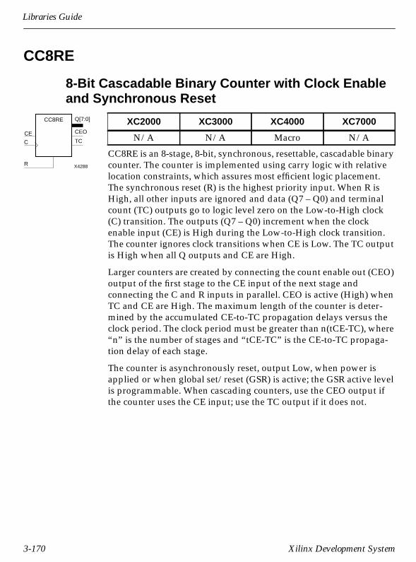
Libraries Guide
CC8RE
8-Bit Cascadable Binary Counter with Clock Enableand Synchronous Reset
CC8RE is an 8-stage, 8-bit, synchronous, resettable, cascadable binarycounter. The counter is implemented using carry logic with relativelocation constraints, which assures most efficient logic placement.The synchronous reset (R) is the highest priority input. When R isHigh, all other inputs are ignored and data (Q7 – Q0) and terminalcount (TC) outputs go to logic level zero on the Low-to-High clock(C) transition. The outputs (Q7 – Q0) increment when the clockenable input (CE) is High during the Low-to-High clock transition.The counter ignores clock transitions when CE is Low. The TC outputis High when all Q outputs and CE are High.
Larger counters are created by connecting the count enable out (CEO)output of the first stage to the CE input of the next stage andconnecting the C and R inputs in parallel. CEO is active (High) whenTC and CE are High. The maximum length of the counter is deter-mined by the accumulated CE-to-TC propagation delays versus theclock period. The clock period must be greater than n(tCE-TC), where“n” is the number of stages and “tCE-TC” is the CE-to-TC propaga-tion delay of each stage.
The counter is asynchronously reset, output Low, when power isapplied or when global set/reset (GSR) is active; the GSR active levelis programmable. When cascading counters, use the CEO output ifthe counter uses the CE input; use the TC output if it does not.
XC2000 XC3000 XC4000 XC7000
N/A N/A Macro N/A
Q[7:0]
X4288
CC8RE
C
R
CE CEO
TC
3-170 Xilinx Development System

Design Elements
TC = (Q7•Q6•Q5•...•Q0•CE)
CEO = (TC•CE)
XC4000 Topology
In the process of combining the logic that loads CEO and TC, the place and routesoftware might map the logic that generates CEO and TC to different functiongenerators. If this mapping occurs, the CEO and TC logic cannot be placed in theuppermost CLB as indicated in the illustration.
Inputs Outputs
R CE C Q7 – Q0 TC CEO
1 X ↑ 0 0 00 0 X No Chg No Chg 00 1 ↑ Inc TC CEO
X3675
Q 7
TC*
CEO*
Q 6
Q 5
Q 4
D 7
D 6
D 5
D 4
Q 3
Q 2
Q 1
Q 0
D 3
D 2
D 1
D 0
Libraries Guide 3-171

Libraries Guide
Figure 3-40 CC8RE XC4000 Implementation
CY4_19INC-FG-1
CEO
TC
VCC
CO
C5
AND2
TQ2
GND
AND2B1XOR2
D0D1
O
S0
M2_1
AND2B1
D0D1
O
S0
M2_1
Q2
RLOC=R3C0.FFX
FDCE
QD
CLR
CECAND2B1
D0D1
O
S0
M2_1
XOR2
Q3
RLOC=R3C0.FFY
FDCE
QD
CLR
CEC
RLOC=R2C0.FFX
Q4
FDCE
QD
CLR
CEC
RLOC=R2C0.FFYQ5
FDCE
QD
CLR
CEC
RLOC=R1C0.FFXQ6
FDCE
QD
CLR
CEC
RLOC=R4C0.F
I1I2I3I4
O
FMAP
RLOC=R1C0.G
I1I2I3I4
O
FMAP
RLOC=R3C0
A0ADD
B1A1B0
CY4
CIN
COUT
COUT0
(F3)(F1)(F2)(G4)(G1)
CARRY MODE
RLOC=R4C0
A0ADD
B1A1B0
CY4
CIN
COUT
COUT0
(F3)(F1)(F2)(G4)(G1)
CARRY MODE
RLOC=R1C0
A0ADD
B1A1B0
CY4
CIN
COUT
COUT0
(F3)(F1)(F2)(G4)(G1)
CARRY MODE
CY4_18
INC-FG-CI
RLOC=R2C0
A0ADD
B1A1B0
CY4
CIN
COUT
COUT0
(F3)(F1)(F2)(G4)(G1)
CARRY MODE
CY4_18
INC-FG-CI
CY4_18
INC-FG-CI
CY4_42EXAMINE-CI
RLOC=R0C0
A0ADD
B1A1B0
CY4
CIN
COUT
COUT0
(F3)(F1)(F2)(G4)(G1)
CARRY MODE
RLOC=R1C0.F
I1I2I3I4
O
FMAP
RLOC=R2C0.G
I1I2I3I4
O
FMAP
RLOC=R2C0.F
I1I2I3I4
O
FMAP
RLOC=R3C0.G
I1I2I3I4
O
FMAP
RLOC=R3C0.F
I1I2I3I4
O
FMAP
RLOC=R4C0.G
I1I2I3I4
O
FMAP
XOR2
D0D1
O
S0
M2_1
XOR2
D0D1
O
S0
M2_1
AND2B1
XOR2
D0D1
O
S0
M2_1
AND2B1
Q1
RLOC=R4C0.FFY
FDCE
QD
CLR
CECXOR2
D0D1
O
S0
M2_1
AND2B1
Q0
RLOC=R4C0.FFX
FDCE
QD
CLR
CEC
AND2B1
D0D1
O
S0
M2_1
XOR2 AND2B1
RLOC=R1C0.FFY
Q7
FDCE
QD
CLR
CEC
CE
CE_M7
C0
C6
C1
R_TQ7
R_TQ6
R_TQ5
R_TQ4
R_TQ3
R_TQ2
R_TQ1
Q7
R_TQ0
Q6
Q0
C6
C5
C4
C3
C2
C1
Q5
Q4
Q3
Q2
Q1C0
R
R
R
R
R
R
R
R
C4
CE_M6
C3
C2
TQ4CE_M4
CE_M5 R_TQ5
TQ7
TQ6
TQ5
TQ3
TQ1
TQ0
CE_M3
CE_M2
CE_M1
CE_M0R_TQ0
R_TQ1
R_TQ3
R_TQ2
R_TQ4
R_TQ6CE
CE
CE
CE
CE
CE
CE
R_TQ7
AND2
Q7
Q3
Q0
Q1
Q2
Q4
Q5
Q6
Q[7:0]
INV
CCE
R
CC8RE.4K
3-172 Xilinx Development System

Design Elements
CC16CE
16-Bit Cascadable Binary Counter with Clock Enableand Asynchronous Clear
CC16CE is a 16-stage, 16-bit, synchronous, clearable, cascadablebinary counter. The counter is implemented using carry logic withrelative location restraints, which assures the most efficient logicplacement. The asynchronous clear (CLR) is the highest priorityinput. When CLR is High, all other inputs are ignored and data(Q15 – Q0) and terminal count (TC) outputs go to logic level zero,independent of clock transitions. The outputs (Q15 – Q0) incrementwhen the clock enable input (CE) is High during the Low-to-Highclock (C) transition. The counter ignores clock transitions when CE isLow. The TC output is High when all Q outputs are High.
Larger counters are created by connecting the count enable out (CEO)output of the first stage to the CE input of the next stage andconnecting the C and CLR inputs in parallel. CEO is active (High)when TC and CE are High. The maximum length of the counter isdetermined by the accumulated CE-to-TC propagation delays versusthe clock period. The clock period must be greater than n(tCE-TC),where “n” is the number of stages and “tCE-TC” is the CE-to-TCpropagation delay of each stage.
The counter is asynchronously reset, output Low, when power isapplied or when global set/reset (GSR) is active. The GSR active levelis programmable. When cascading counters, use the CEO output ifthe counter uses the CE input; use the TC output if it does not.
XC2000 XC3000 XC4000 XC7000
N/A N/A Macro N/A
Q[15:0]
X4286
CC16CE
C
CLR
CE CEO
TC
Libraries Guide 3-173

Libraries Guide
TC = (Q15•Q14•Q13•Q12•...•Q0)
CEO = (TC•CE)
XC4000 Topology
In the process of combining the logic that loads CEO and TC, the place and routesoftware might map the logic that generates CEO and TC to different functiongenerators. If this mapping occurs, the CEO and TC logic cannot be placed in theuppermost CLB as indicated in the illustration.
Inputs Outputs
CLR CE C Q15 – Q0 TC CEO
1 X X 0 0 00 0 X No Chg No Chg 00 1 ↑ Inc TC CEO
X3672
Q 15
TC*
CEO*
Q 14
Q 13
Q 12
Q 11
Q 10
Q 9
Q 8
D 9
D 8
Q 7
Q 6
Q 5
Q 4
D 7
D 6
D 5
D 4
Q 3
Q 2
Q 1
Q 0
D 3
D 2
D 1
D 0
D 15
D 14
D 13
D 12
D 11
D 10
3-174 Xilinx Development System

Design Elements
CC16CLE
16-Bit Loadable Cascadable Binary Counter withClock Enable and Asynchronous Clear
CC16CLE is a 16-stage, 16-bit, synchronous, loadable, clearable,cascadable binary counter. The counter is implemented using carrylogic with relative location constraints, which assures the most effi-cient logic placement.
The asynchronous clear (CLR) is the highest priority input. WhenCLR is High, all other inputs are ignored and data (Q15 – Q0) andterminal count (TC) outputs go to logic level zero, independent ofclock transitions. The data on the D15 – D0 inputs is loaded into thecounter when the load enable input (L) is High during the Low-to-High clock (C) transition, independent of the state of clock enable(CE). The outputs (Q15 – Q0) increment when CE is High during theLow-to-High clock transition. The counter ignores clock transitionswhen CE is Low. The TC output is High when all Q outputs are High.
Larger counters are created by connecting the count enable out (CEO)output of the first stage to the CE input of the next stage andconnecting the C, L, and CLR inputs in parallel. CEO is active (High)when TC and CE are High. The maximum length of the counter isdetermined by the accumulated CE-to-TC propagation delays versusthe clock period. The clock period must be greater than n(tCE-TC),where “n” is the number of stages and “tCE-TC” is the CE-to-TCpropagation delay of each stage.
The counter is asynchronously reset, output Low, when power isapplied or when global set/reset (GSR) is active. The GSR active levelis programmable. When cascading counters, use the CEO output ifthe counter uses the CE input; use the TC output if it does not.
XC2000 XC3000 XC4000 XC7000
N/A N/A Macro N/A
Q[15:0]
X4284
CC16CLE
C
CLR
CE
D[15:0]
L
CEO
TC
Libraries Guide 3-175

Libraries Guide
TC = (Q15•Q14•Q13•Q12•...•Q0)
CEO = (TC•CE)
dn = state of referenced input one set-up time prior to active clock transition
XC4000 Topology
In the process of combining the logic that loads CEO and TC, the place and routesoftware might map the logic that generates CEO and TC to different functiongenerators. If this mapping occurs, the CEO and TC logic cannot be placed in theuppermost CLB as indicated in the illustration.
Inputs Outputs
CLR L CE C D15 – D0 Q15 – Q0 TC CEO
1 X X X X 0 0 00 1 X X D d15 – d0 TC CEO0 0 0 X X No Chg No Chg 00 0 1 ↑ X Inc TC CEO
X3674
TC*
CEO*
Q 15
Q 14
Q 13
Q 12
D 15
D 14
D 13
D 12
Q 11
Q 10
Q 9
Q 8
D 11
D 10
D 9
D 8
Q 7
Q 6
Q 5
Q 4
D 7
D 6
D 5
D 4
Q 3
Q 2
Q 1
Q 0
D 3
D 2
D 1
D 0
3-176 Xilinx Development System

Design Elements
CC16CLED
16-Bit Loadable Cascadable Bidirectional BinaryCounter with Clock Enable and Asynchronous Clear
CC16CLED is a 16-stage, 16-bit, synchronous, loadable, clearable,cascadable, bidirectional binary counter. The counter is implementedusing carry logic with relative location constraints, which assuresmost efficient logic placement.
The asynchronous clear (CLR) is the highest priority input. WhenCLR is High, all other inputs are ignored and data (Q15 – Q0) andterminal count (TC) outputs go to logic level zero, independent ofclock transitions. The data on the D15 – D0 inputs is loaded into thecounter when the load enable input (L) is High during the Low-to-High clock (C) transition, independent of the state of clock enable(CE). The outputs (Q15 – Q0) decrement when CE is High and UP isLow during the Low-to-High clock transition. The outputs (Q15 –Q0) increment when CE and UP are High. The counter ignores clocktransitions when CE is Low.
For counting up, the TC output is High when all Q outputs and UPare High. For counting down, the TC output is High when all Qoutputs and UP are Low. To cascade counters, the count enable out(CEO) output of each counter is connected to the CE pin of the nextstage. The clock, UP, L, and CLR inputs are connected in parallel.CEO is active (High) when TC and CE are High. The maximumlength of the counter is determined by the accumulated CE-to-TCpropagation delays versus the clock period. The clock period must begreater than n(tCE-TC), where “n” is the number of stages and“tCE-TC” is the CE-to-TC propagation delay of each stage.
The counter is asynchronously reset, output Low, when power isapplied or when global set/reset (GSR) is active. The GSR active levelis programmable. When cascading counters, use the CEO output ifthe counter uses the CE input; use the TC output if it does not.
XC2000 XC3000 XC4000 XC7000
N/A N/A Macro N/A
Q[15:0]
X4285
CC16CLED
C
CLR
CE
D[15:0]
L
UP
CEO
TC
Libraries Guide 3-177

Libraries Guide
TC = (Q15•Q14•Q13•...•Q0•UP) + (Q15•Q14•Q13•...•Q0•UP)
CEO = (TC•CE)
dn = state of referenced clock one set-up time prior to active clock transition
XC4000 Topology
In the process of combining the logic that loads CEO and TC, the place and routesoftware might map the logic that generates CEO and TC to different functiongenerators. If this mapping occurs, the CEO and TC logic cannot be placed in theuppermost CLB as indicated in the illustration.
Inputs Outputs
CLR L CE C UP D15 – D0 Q15 – Q0 TC CEO
1 X X X X X 0 0 00 1 X X X D d15 – d0 TC CEO0 0 0 X X X No Chg No Chg 00 0 1 ↑ 1 X Inc TC CEO0 0 1 ↑ 0 X Dec TC CEO
X4340
D 15
D 14
D 13
D 12
TC*
CEO*
Q 15
Q 14
Q 13
Q 12
Q 11
Q 10
Q 9
Q 8
D 11
D 10
D 9
D 8
D 7
D 6
D 5
D 4
Q 7
Q 6
Q 5
Q 4
Q 3
Q 2
Q 1
Q 0
D 3
D 2
D 1
D 0
3-178 Xilinx Development System

Design Elements
CC16RE
16-Bit Cascadable Binary Counter with Clock Enableand Synchronous Reset
CC16RE is a 16-stage, 16-bit, synchronous, resettable, cascadablebinary counter. The counter is implemented using carry logic withrelative location constraints, which assures most efficient logic place-ment. The synchronous reset (R) is the highest priority input. When Ris High, all other inputs are ignored and data (Q15 – Q0) and terminalcount (TC) outputs go to logic level zero on the Low-to-High clock(C) transition. The outputs (Q15 – Q0) increment when the clockenable input (CE) is High during the Low-to-High clock transition.The counter ignores clock transitions when CE is Low. The TC outputis High when all Q outputs and CE are High.
Larger counters are created by connecting the count enable out (CEO)output of the first stage to the CE input of the next stage andconnecting the C and R inputs in parallel. CEO is active (High) whenTC and CE are High. The maximum length of the counter is deter-mined by the accumulated CE-to-TC propagation delays versus theclock period. The clock period must be greater than n(tCE-TC), where“n” is the number of stages and “tCE-TC” is the CE-to-TC propaga-tion delay of each stage.
The counter is asynchronously reset, output Low, when power isapplied or when global set/reset (GSR) is active. The GSR active levelis programmable. When cascading counters, use the CEO output ifthe counter uses the CE input; use the TC output if it does not.
XC2000 XC3000 XC4000 XC7000
N/A N/A Macro N/A
Q[15:0]
X4283
CC16RE
C
R
CE CEO
TC
Libraries Guide 3-179

Libraries Guide
TC = (Q15•Q14•Q13•...•Q0)
CEO = (TC•CE)
XC4000 Topology
In the process of combining the logic that loads CEO and TC, the place and routesoftware might map the logic that generates CEO and TC to different functiongenerators. If this mapping occurs, the CEO and TC logic cannot be placed in theuppermost CLB as indicated in the illustration.
Inputs Outputs
R CE C Q15 – Q0 TC CEO
1 X ↑ 0 0 00 0 X No Chg No Chg 00 1 ↑ Inc TC CEO
X3676
Q 15
TC*
CEO*
Q 14
Q 13
Q 12
D 15
D 14
D 13
D 12
Q 11
Q 10
Q 9
Q 8
D 11
D 10
D 9
D 8
Q 7
Q 6
Q 5
Q 4
D 7
D 6
D 5
D 4
Q 3
Q 2
Q 1
Q 0
D 3
D 2
D 1
D 0
3-180 Xilinx Development System

Design Elements
CD4CE
4-Bit Cascadable BCD Counter with Clock Enableand Asynchronous Clear
CD4CE is a 4-stage, 4-bit, synchronous, clearable, cascadable binary-coded-decimal (BCD) counter. The asynchronous clear input (CLR) isthe highest priority input. When CLR is High, all other inputs areignored and data (Q3 – Q0) and terminal count (TC) outputs go tologic level zero, independent of clock transitions. The outputs(Q3 – Q0) increment when clock enable (CE) is High during the Low-to-High clock (C) transition. The counter ignores clock transitionswhen CE is Low. The TC output is High when Q3 and Q0 are Highand Q2 and Q1 are Low.
The counter recovers from any of six possible illegal states andreturns to a normal count sequence within two clock cycles forXC2000, XC3000, and XC4000 architectures, as shown in thefollowing state diagram. For XC7000, the counter resets to zero orrecovers within the first clock cycle.
Larger counters are created by connecting the count enable out (CEO)output of the first stage to the CE input of the next stage andconnecting the CLR and clock inputs in parallel. CEO is active (High)when TC and CE are High. The maximum length of the counter isdetermined by the accumulated CE-to-TC propagation delays versusthe clock period. The clock period must be greater than n(tCE-TC),where “n” is the number of stages and “tCE-TC” is the CE-to-TCpropagation delay of each stage.
XC2000 XC3000 XC4000 XC7000
Macro Macro Macro PrimitiveQ2
X4369
CD4CE
C
CLR
CE
Q3
TC
Q1
Q0
CEO
0 1 2 3 4
F 5
E 6
D 7
C B A 9 8
X2355
Libraries Guide 3-181
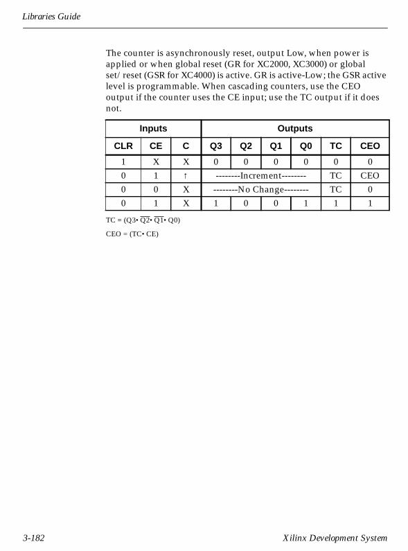
Libraries Guide
The counter is asynchronously reset, output Low, when power isapplied or when global reset (GR for XC2000, XC3000) or globalset/reset (GSR for XC4000) is active. GR is active-Low; the GSR activelevel is programmable. When cascading counters, use the CEOoutput if the counter uses the CE input; use the TC output if it doesnot.
TC = (Q3•Q2•Q1•Q0)
CEO = (TC•CE)
Inputs Outputs
CLR CE C Q3 Q2 Q1 Q0 TC CEO
1 X X 0 0 0 0 0 00 1 ↑ --------Increment-------- TC CEO0 0 X --------No Change-------- TC 00 1 X 1 0 0 1 1 1
3-182 Xilinx Development System
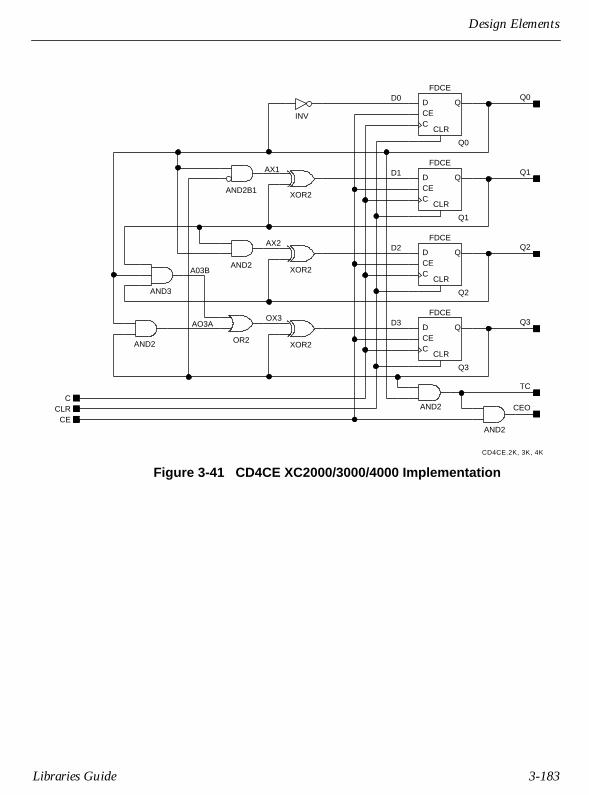
Design Elements
Figure 3-41 CD4CE XC2000/3000/4000 Implementation
AND2
Q3
Q0
FDCE
QD
CLR
CEC
Q1
FDCE
QD
CLR
CEC
Q2
FDCE
QD
CLR
CEC
Q3
FDCE
QD
CLR
CEC
C
AND2
XOR2
INV
AND2B1
XOR2AND2
OR2XOR2
AND3
CLR
D0
AO3A
AX1
AX2
OX3
A03B
Q1D1
D2
D3
Q2
CE
TC
Q0
CEOAND2
CD4CE.2K, 3K, 4K
Libraries Guide 3-183

Libraries Guide
CD4CLE
4-Bit Loadable Cascadable BCD Counter with ClockEnable and Asynchronous Clear
CD4CLE is a 4-stage, 4-bit, synchronous, loadable, clearable, binary-coded-decimal (BCD) counter. The asynchronous clear input (CLR) isthe highest priority input. When CLR is High, all other inputs areignored and the data (Q3 – Q0) and terminal count (TC) outputs go tologic level zero, independent of clock transitions. The data on theD3 – D0 inputs is loaded into the counter when the load enable input(L) is High during the Low-to-High clock (C) transition. The outputs(Q3 – Q0) increment when clock enable input (CE) is High during theLow- to-High clock transition. The counter ignores clock transitionswhen CE is Low. The TC output is High when Q3 and Q0 are Highand Q2 and Q1 are Low.
The counter recovers from any of six possible illegal states andreturns to a normal count sequence within two clock cycles forXC2000, XC3000, and XC4000, as shown in the following statediagram. For XC7000, the counter resets to zero or recovers within thefirst clock cycle.
Larger counters are created by connecting the count enable out (CEO)output of the first stage to the CE input of the next stage andconnecting the CLR, L, and C inputs in parallel. CEO is active (High)when TC and CE are High. The maximum length of the counter isdetermined by the accumulated CE-to-TC propagation delays versusthe clock period. The clock period must be greater than n(tCE-TC),
XC2000 XC3000 XC4000 XC7000
Macro Macro Macro Primitive
X4370
CD4CLE
L
CE
C
D3
D2
D1
D0
Q3
Q2
Q1
Q0
CLR
CEO
TC
0 1 2 3 4
F 5
E 6
D 7
C B A 9 8
X2355
3-184 Xilinx Development System

Design Elements
where “n” is the number of stages and “tCE-TC” is the CE-to-TCpropagation delay of each stage.
The counter is asynchronously reset, output Low, when power isapplied or when global reset (GR for XC2000, XC3000) or globalset/reset (GSR for XC4000) is active. GR is active-Low; the GSR activelevel is programmable. When cascading counters, use the CEOoutput if the counter uses the CE input; use the TC output if it doesnot.
TC = (Q3•Q2•Q1•Q0)
CEO = (TC•CE)
dn = state of referenced input one set-up time prior to active clock transition
Inputs Outputs
CLR L CE D3 – D0 C Q3 Q2 Q1 Q0 TC CEO
1 X X X X 0 0 0 0 0 00 1 X D3 – D0 ↑ d3 d2 d1 d0 TC CEO0 0 1 X ↑ ---------Increment---------- TC CEO0 0 0 X X --------No Change--------- TC 00 0 1 X X 1 0 0 1 1 1
Libraries Guide 3-185

Libraries Guide
Figure 3-42 CD4CLE XC2000/3000/4000 Implementation
AND4B2
TQ03Q3
CET
CLR
QLD
C
FTCLE
D2
VCC+5
T2
OR2
T3TQ2
T1
AND2
C
CLR
D1
D0
Q1
CET
CLR
QLD
C
FTCLE
Q2
CET
CLR
QLD
C
FTCLE
Q0
CET
CLR
QLD
C
FTCLE
AND3B1
AND3
L
D3
AND2
Q0
CE
Q2
Q1
AND2
TC
CEO
Q3
CD4CLE.4K
3-186 Xilinx Development System

Design Elements
CD4RE
4-Bit Cascadable BCD Counter with Clock Enableand Synchronous Reset
CD4RE is a 4-stage, 4-bit, synchronous, resettable, cascadable binary-coded-decimal (BCD) counter. The synchronous reset input (R) is thehighest priority input. When R is High, all other inputs are ignoredand (Q3 – Q0) and terminal count (TC) outputs go to logic level zeroon the Low-to-High clock (C) transition. The outputs (Q3 – Q0) incre-ment when the clock enable input (CE) is High during the Low-to-High clock transition. The counter ignores clock transitions when CEis Low. The TC output is High when Q3 and Q0 are High and Q2 andQ1 are Low.
The counter recovers from any of six possible illegal states andreturns to a normal count sequence within two clock cycles forXC2000, XC3000, and XC4000, as shown in the following statediagram. For XC7000, the counter resets to zero or recovers withinthe first clock cycle.
Larger counters are created by connecting the count enable out (CEO)output of the first stage to the CE input of the next stage andconnecting the R and clock inputs in parallel. CEO is active (High)when TC and CE are High. The maximum length of the counter isdetermined by the accumulated CE-to-TC propagation delays versusthe clock period. The clock period must be greater than n(tCE-TC)where “n” is the number of stages and “tCE-TC” is the CE-to-TCpropagation delay of each stage.
XC2000 XC3000 XC4000 XC7000
Macro Macro Macro PrimitiveQ2
X4371
CD4RE
C
R
CE CEO
TC
Q1
Q0
Q3
0 1 2 3 4
F 5
E 6
D 7
C B A 9 8
X2355
Libraries Guide 3-187

Libraries Guide
The counter is asynchronously reset, output Low, when power isapplied or when global reset (GR for XC2000, XC3000) or globalset/reset (GSR for XC4000) is active. GR is active-Low; the GSR activelevel is programmable. When cascading counters, use the CEOoutput if the counter uses the CE input; use the TC output if it doesnot.
TC = (Q3•Q2•Q1•Q0)
CEO = (TC•CE)
Inputs Outputs
R CE C Q3 Q2 Q1 Q0 TC CEO
1 X ↑ 0 0 0 0 0 00 1 ↑ ---------Increment-------- TC CEO0 0 X --------No Change-------- TC 00 1 X 1 0 0 1 1 1
3-188 Xilinx Development System

Design Elements
Figure 3-43 CD4RE XC2000/3000/4000 Implementation
R
C
AND2
Q1
AND4B2
Q3
TC
CEO
Q2
A03B
OX3
AX2
AX1
AO3A
AND3
XOR2OR2
AND2XOR2
AND2B1
INV
XOR2
Q0
D1
D2
D3
D0
CE
AND2
Q3
FDRE
R
QD
CE
C
Q2
FDRE
R
QD
CE
C
Q1
FDRE
R
QD
CE
C
Q0
FDRE
R
QD
CE
C
CD4RE.4K
Libraries Guide 3-189

Libraries Guide
CD4RLE
4-Bit Loadable Cascadable BCD Counter with ClockEnable and Synchronous Reset
CD4RLE is a 4-stage, 4-bit, synchronous, loadable, resettable, binary-coded-decimal (BCD) counter. The synchronous reset input (R) is thehighest priority input. When R is High, all other inputs are ignoredand the data (Q3 – Q0) and terminal count (TC) outputs go to logiclevel zero on the Low-to-High clock transitions. The data on the D3 –D0 inputs is loaded into the counter when the load enable input (L) isHigh during the Low-to-High clock (C) transition. The outputs(Q3 – Q0) increment when the clock enable input (CE) is High duringthe Low-to-High clock transition. The counter ignores clock transi-tions when CE is Low. The TC output is High when Q3 and Q0 areHigh and Q2 and Q1 are Low.
The counter recovers from any of six possible illegal states andreturns to a normal count sequence within two clock cyclesforXC2000, XC3000, and XC4000, as shown in the following statediagram. For XC7000, the counter resets to zero or recovers within thefirst clock cycle.
Larger counters are created by connecting the count enable out (CEO)output of the first stage to the CE input of the next stage andconnecting the R, L, and C inputs in parallel. CEO is active (High)when TC and CE are High. The maximum length of the counter isdetermined by the accumulated CE-to-TC propagation delays versusthe clock period. The clock period must be greater than n(tCE-TC),
XC2000 XC3000 XC4000 XC7000
Macro Macro Macro Primitive
X4372
CD4RLE
L
CE
C
D3
D2
D1
D0
Q3
Q2
Q1
Q0
R
CEO
TC
0 1 2 3 4
F 5
E 6
D 7
C B A 9 8
X2355
3-190 Xilinx Development System

Design Elements
where “n” is the number of stages and “tCE-TC” is the CE-to-TCpropagation delay of each stage.
The counter is asynchronously reset, output Low, when power isapplied or when global reset (GR for XC2000, XC3000) or globalset/reset (GSR for XC4000) is active. GR is active-Low; the GSR activelevel is programmable. When cascading counters, use the CEOoutput if the counter uses the CE input; use the TC output if it doesnot.
TC = (Q3•Q2•Q1•Q0)
CEO = (TC•CE)
dn = state of referenced input one set-up time prior to active clock transition
Inputs Outputs
R L CE D3 – D0 C Q3 Q2 Q1 Q0 TC CEO
1 X X X ↑ 0 0 0 0 0 00 1 X D3 – D0 ↑ d3 d2 d1 d0 TC CEO0 0 1 X ↑ ----------Increment--------- TC CEO0 0 0 X X --------No Change--------- TC 00 0 1 X X 1 0 0 1 1 1
Libraries Guide 3-191

Libraries Guide
Figure 3-44 CD4RLE XC2000/3000/4000 Implementation
Q3
Q2
CEO
AND2
TC
AND4B2
GND
TQ03
Q1
Q0
T1
VCC
Q3
FTRSLE
CET
S
R
QLD
CAND3
C
AND2 OR2
D3TQ2 T3
R
Q2
FTRSLE
CET
S
R
QLD
C
D2
Q0
FTRSLE
CET
S
R
QLD
C
Q1
FTRSLE
CET
S
R
QLD
CAND3B1
D0
D1
L
T2
AND2
CE
CD4RLE.2K, 3K, 4K
3-192 Xilinx Development System

Design Elements
CJ4CE
4-Bit Johnson Counter with Clock Enable andAsynchronous Clear
CJ4CE is a clearable Johnson/shift counter. The asynchronous clear(CLR) input, when High, overrides all other inputs and causes thedata outputs (Q3 – Q0) to go to logic level zero, independent of clock(C) transitions. The counter increments (shifts Q0 to Q1, Q1 to Q2,andso forth) when the clock enable input (CE) is High during the Low-to-High clock transition. Clock transitions are ignored when CE is Low.The Q3 output is inverted and fed back to input Q0 to provide contin-uous counting operation.
The counter is asynchronously reset, output Low, when power isapplied or when global reset (GR for XC2000, XC3000) or globalset/reset (GSR for XC4000) is active. GR is active-Low; the GSR activelevel is programmable.
qn = state of referenced output one set-up time prior to active clock transition
XC2000 XC3000 XC4000 XC7000
Macro Macro Macro Primitive
Inputs Outputs
CLR CE C Q0 Q1 Q2 Q3
1 X X 0 0 0 00 0 X --------No Change--------0 1 ↑ q3 q0 q1 q2
Q1
X4112CLR
C
CJ4CE
CE Q2
Q3
Q0
Libraries Guide 3-193

Libraries Guide
Figure 3-45 CJ4CE XC2000/3000/4000 Implementation
Q3
FDCEQD
CLR
CEC
Q2
FDCEQD
CLR
CEC
Q1
FDCEQD
CLR
CEC
Q0
FDCEQD
CLR
CEC
INV
Q3
Q2
Q1
CCE
CLR
Q0Q3B
3-194 Xilinx Development System

Design Elements
CJ4RE
4-Bit Johnson Counter with Clock Enable andSynchronous Reset
CJ4RE is a resettable Johnson/shift counter. The synchronous reset(R) input, when High, overrides all other inputs causes the dataoutputs (Q3 – Q0) to go to logic level zero during the Low-to-Highclock (C) transition. The counter increments (shifts Q0 to Q1, Q1 toQ2, and so forth) when the clock enable input (CE) is High during theLow-to-High clock transition. Clock transitions are ignored when CEis Low. The Q3 output is inverted and fed back to input Q0 to providecontinuous counting operation.
The counter is asynchronously reset, output Low, when power isapplied or when global reset (GR for XC2000, XC3000) or globalset/reset (GSR for XC4000) is active. GR is active-Low; the GSR activelevel is programmable.
qn = state of referenced output one set-up time prior to active clock transition
XC2000 XC3000 XC4000 XC7000
Macro Macro Macro Primitive
Inputs Outputs
R CE C Q0 Q1 Q2 Q3
1 X ↑ 0 0 0 00 0 X --------No Change--------0 1 ↑ q3 q0 q1 q2
Q1
X4113R
C
CJ4RE
CE Q2
Q3
Q0
Libraries Guide 3-195
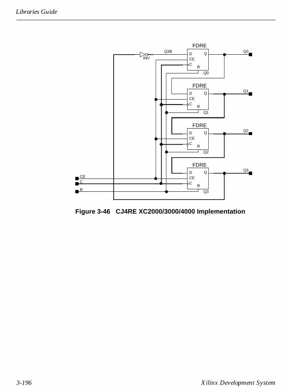
Libraries Guide
Figure 3-46 CJ4RE XC2000/3000/4000 Implementation
Q0
Q0
FDRE
R
QDCEC
Q1
FDRE
R
QDCEC
Q3
FDRE
R
QDCEC
Q2
FDRE
R
QDCEC
R
C
Q2
Q1
Q3
INV
Q3B
CE
3-196 Xilinx Development System

Design Elements
CJ5CE
5-Bit Johnson Counter with Clock Enable andAsynchronous Clear
CJ5CE is a clearable Johnson/shift counter. The asynchronous clear(CLR) input, when High, overrides all other inputs and causes thedata outputs (Q4 – Q0) to go to logic level zero, independent of clock(C) transitions. The counter increments (shifts Q0 to Q1, Q1 to Q2,and so forth) when the clock enable input (CE) is High during theLow-to-High clock transition. Clock transitions are ignored when CEis Low. The Q4 output is inverted and fed back to input Q0 to providecontinuous counting operation.
The counter is asynchronously reset, output Low, when power isapplied or when global reset (GR for XC2000, XC3000) or globalset/reset (GSR for XC4000) is active. GR is active-Low; the GSR activelevel is programmable.
qn = state of referenced output one set-up time prior to active clock transition
XC2000 XC3000 XC4000 XC7000
Macro Macro Macro Primitive
Inputs Outputs
CLR CE C Q0 Q1 Q2 Q3 Q4
1 X X 0 0 0 0 00 0 X ------------No Change------------0 1 ↑ q4 q0 q1 q2 q3
Q2
X4114CLR
C
CJ5CE
CE Q3
Q4
Q1
Q0
Libraries Guide 3-197
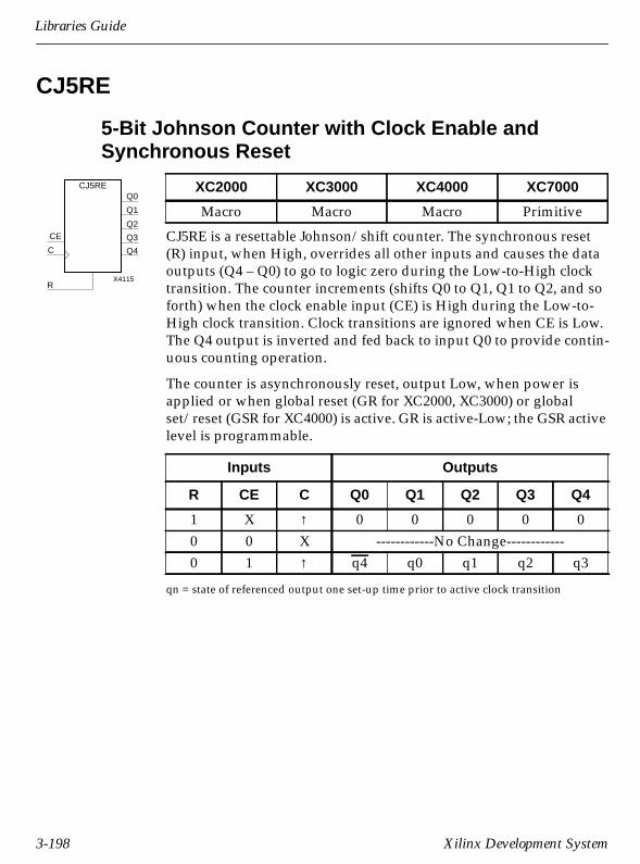
Libraries Guide
CJ5RE
5-Bit Johnson Counter with Clock Enable andSynchronous Reset
CJ5RE is a resettable Johnson/shift counter. The synchronous reset(R) input, when High, overrides all other inputs and causes the dataoutputs (Q4 – Q0) to go to logic zero during the Low-to-High clocktransition. The counter increments (shifts Q0 to Q1, Q1 to Q2, and soforth) when the clock enable input (CE) is High during the Low-to-High clock transition. Clock transitions are ignored when CE is Low.The Q4 output is inverted and fed back to input Q0 to provide contin-uous counting operation.
The counter is asynchronously reset, output Low, when power isapplied or when global reset (GR for XC2000, XC3000) or globalset/reset (GSR for XC4000) is active. GR is active-Low; the GSR activelevel is programmable.
qn = state of referenced output one set-up time prior to active clock transition
XC2000 XC3000 XC4000 XC7000
Macro Macro Macro Primitive
Inputs Outputs
R CE C Q0 Q1 Q2 Q3 Q4
1 X ↑ 0 0 0 0 00 0 X ------------No Change------------0 1 ↑ q4 q0 q1 q2 q3
Q2
X4115R
C
CJ5RE
CE Q3
Q4
Q1
Q0
3-198 Xilinx Development System
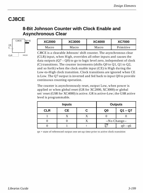
Design Elements
CJ8CE
8-Bit Johnson Counter with Clock Enable andAsynchronous Clear
CJ8CE is a clearable Johnson/shift counter. The asynchronous clear(CLR) input, when High, overrides all other inputs and causes thedata outputs (Q7 – Q0) to go to logic level zero, independent of clock(C) transitions. The counter increments (shifts Q0 to Q1, Q1 to Q2,and so forth) when the clock enable input (CE) is High during theLow-to-High clock transition. Clock transitions are ignored when CEis Low. The Q7 output is inverted and fed back to input Q0 to providecontinuous counting operation.
The counter is asynchronously reset, output Low, when power isapplied or when global reset (GR for XC2000, XC3000) or globalset/reset (GSR for XC4000) is active. GR is active-Low; the GSR activelevel is programmable.
qn = state of referenced output one set-up time prior to active clock transition
XC2000 XC3000 XC4000 XC7000
Macro Macro Macro Primitive
Inputs Outputs
CLR CE C Q0 Q1 – Q7
1 X X 0 00 0 X --No Change--0 1 ↑ q7 q0 – q6
X4118
CJ8CE
C
CLR
CE
Q[7:0]
Libraries Guide 3-199

Libraries Guide
Figure 3-47 CJ8CE XC2000/3000/4000 Implementation
CCLR
Q0
FDCEQD
CLRCEC
Q1
FDCEQD
CLRCEC
Q[7:0]Q7
Q4
Q6
Q5
Q7Q3
Q2
Q1
Q0 Q3
Q2
FDCEQD
CLRCEC
Q3
FDCEQD
CLRCEC
Q4
FDCEQD
CLRCEC
Q5
FDCEQD
CLRCEC
Q6
FDCEQD
CLRCEC
Q7
FDCEQD
CLRCEC
INV
CE
Q7B
3-200 Xilinx Development System
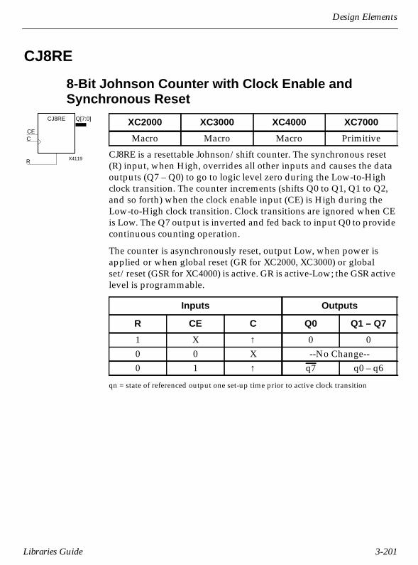
Design Elements
CJ8RE
8-Bit Johnson Counter with Clock Enable andSynchronous Reset
CJ8RE is a resettable Johnson/shift counter. The synchronous reset(R) input, when High, overrides all other inputs and causes the dataoutputs (Q7 – Q0) to go to logic level zero during the Low-to-Highclock transition. The counter increments (shifts Q0 to Q1, Q1 to Q2,and so forth) when the clock enable input (CE) is High during theLow-to-High clock transition. Clock transitions are ignored when CEis Low. The Q7 output is inverted and fed back to input Q0 to providecontinuous counting operation.
The counter is asynchronously reset, output Low, when power isapplied or when global reset (GR for XC2000, XC3000) or globalset/reset (GSR for XC4000) is active. GR is active-Low; the GSR activelevel is programmable.
qn = state of referenced output one set-up time prior to active clock transition
XC2000 XC3000 XC4000 XC7000
Macro Macro Macro Primitive
Inputs Outputs
R CE C Q0 Q1 – Q7
1 X ↑ 0 00 0 X --No Change--0 1 ↑ q7 q0 – q6
X4119
CJ8RE
C
R
CE
Q[7:0]
Libraries Guide 3-201
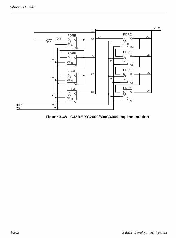
Libraries Guide
Figure 3-48 CJ8RE XC2000/3000/4000 Implementation
CECR
INV
Q3Q0
Q1
Q2
Q3 Q7
Q5
Q6
Q4
Q7
Q[7:0]
Q7
FDRE
R
QDCEC
Q6
FDRE
R
QDCEC
Q5
FDRE
R
QDCEC
Q4
FDRE
R
QDCEC
Q3
FDRE
R
QDCEC
Q2
FDRE
R
QDCEC
Q1
FDRE
R
QDCEC
Q0
FDRE
R
QDCEC
Q7B
3-202 Xilinx Development System

Design Elements
CLB
CLB Configuration Symbol
The CLB symbol enables you to manually specify a CLB configura-tion. It allows you to enter portions of a logic design directly in termsof the physical CLB, rather than schematically. Using the CLB symbolprovides precise partitioning control and requires knowledge of theCLB architecture. Use it in place of the equivalent captured logic andnot in conjunction with it.
XC2000 XC3000 XC4000 XC7000
Primitive Primitive N/A N/A
X4650
RD
K
EC
O1
E
D
C
B
A
Y
X
CLB
X4647
K
D
C
BCLBA
Y
XCLB
XC2000
XC3000
Libraries Guide 3-203
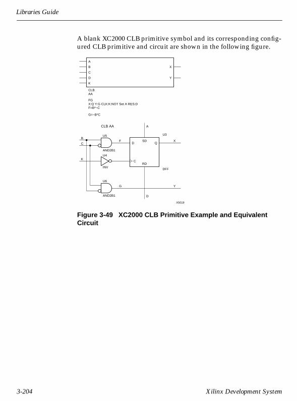
Libraries Guide
A blank XC2000 CLB primitive symbol and its corresponding config-ured CLB primitive and circuit are shown in the following figure.
Figure 3-49 XC2000 CLB Primitive Example and EquivalentCircuit
X5019
CLBAA
FGX:Q Y:G CLK:K:NOT Set A RES:DF=B*~C
A
B
C
X
D
K
Y
QD
C
F X
U3
SD
RD
U5
AND2B1
U4
INV
G
U6
AND2B1
Y
DFF
A
D
B
C
K
CLB AA
G=~B*C
3-204 Xilinx Development System

Design Elements
A blank XC3000 CLB primitive symbol and its corresponding config-ured CLB primitive and circuit are shown in the following figure.
Figure 3-50 XC3000 CLB Primitive Example and EquivalentCircuit
CLB symbol pins correspond to actual CLB pins. Signals connected tothese pins in a schematic are connected to the corresponding CLBpins in the design. You must specify the BASE, CONFIG, andEQUATE commands for the CLB. These commands are entered onthe schematic and the translator puts them into the CFG records inthe LCA Xilinx netlist file. It is not necessary for the translatorprogram to parse the commands specifying the CLB configuration.The mapping program from the LCA Xilinx netlist to the LCA designchecks these commands for errors.
X5021
CLB
FGX:QX Y:QY DX:Y DY:G CLK:K ENCLK:ECF=A*B*E*QYG=QX*A*E*QY
A
B
C X
D
E
Y
QD
CE
F X
U4U3
AND4
FDCE
A
O1
EC
K
RD
AA
BE
C
QD
CE
G Y
U5U6
AND4
FDCE
D
C
K
CE
Libraries Guide 3-205

Libraries Guide
The configuration commands must be consistent with the connec-tions. For example, if you use the A input in an equation, connect asignal to the A pin. Refer to the applicable CAE tool interface userguide for more information on specifying the CLB configurationcommands in the schematic.
You can specify the location of a CLB on the device using the LOCattribute. When specifying the LOC attribute, a valid CLB name (AA,AB, and so forth) must be used. Refer to the “Attributes, Constraints,and Carry Logic” chapter for more information on the LOC attribute.
3-206 Xilinx Development System

Design Elements
CLBMAP
Logic-Partitioning Control Symbol
The CLBMAP symbol is used to control logic partitioning intoXC2000 and XC3000 family CLBs. Unlike the CLB symbol, theCLBMAP symbol is not a substitute for logic. It is used in addition tocombinatorial gates, latches, and flip-flops for mapping control.
At the schematic level, you can implement a portion of logic usinggates, latches, and flip-flops and specify that the logic be groupedinto a single CLB by using the CLBMAP symbol. You must name thesignals that are the inputs and outputs of the CLB, then draw thesignals to appropriate pins of the CLBMAP symbol or name theCLBMAP signals and logic signals correspondingly. The symbol canhave unconnected pins, but all signals on the logic group to bemapped must be specified on a symbol pin.
CLBMAP primitives and equivalent circuits are shown for XC2000and XC3000 families in the following figures.
XC2000 XC3000 XC4000 XC7000
Primitive Primitive N/A N/A
X4648
K
C
A
D
BX
Y
CLBMAP
XC2000
XC3000
X4651
RD
EC
E
K
DI
X
Y
D
B
C
A CLBMAP
Libraries Guide 3-207

Libraries Guide
Figure 3-51 XC2000 CLBMAP Primitive Example and Equivalent
X4454
U10
AND2
U2
IBUF
A0INU1
PAD
A0U9
XOR2
U4
IBUF
B0INU3
PAD
B0
U6
IBUF
A1INU5
PAD
A1U11
XOR2
U8
IBUF
B1INU7
PAD
B1
U12
XOR2
U13
AND2
U14
AND2
U15
AND2
U16
XOR3
U17
OBUF
SUM0 S0
U18
OBUF
SUM1 S1
U19
OBUF
SUM2 S2
A
BSUM1
D
K
SUM2
X
Y
CLBMAP
A0
B0
A1
B1C
3-208 Xilinx Development System

Design Elements
Figure 3-52 XC3000 CLBMAP Primitive Example and Equivalent
Use the MAP=type parameter with the CLBMAP symbol to furtherdefine how much latitude you want to give the mapping program.The following table shows MAP option characters and their mean-ings.
Character Function
P PinsC Closed – Adding logic to or removing logic
from the CLB is not allowed.L Locked – Locking CLB pinsO Open – Adding logic to or removing logic from
the CLB is allowed.U Unlocked – No locking on CLB pins.
X5022
U10
AND2
U2
IBUF
A0INU1
PAD
A0U9
XOR2
U4
IBUF
B0INU3
PAD
B0
U6
IBUF
A1INU5
PAD
A1U11
XOR2
U8
IBUF
B1INU7
PAD
B1
U12
XOR2
U13
AND2
U14
AND2
U15
AND2
U16
XOR3
U17
OBUF
SUM0 S0
U18
OBUF
SUM1 S1
U19
OBUF
SUM2 S2
A
BSUM1
D
E
DISUM2
K
RD
X
Y
CLBMAP
A0
A1
B0
B1C
EC
Libraries Guide 3-209

Libraries Guide
Possible types of MAP parameters for FMAP are: MAP=PUC,MAP=PLC, MAP=PLO, and MAP=PUO. The default parameter isPUC. If one of the “open” parameters is used (PLO or PUO), only theoutput signals must be specified.
You can lock individual pins using the “P” (Pin lock) parameter onthe CLBMAP pin in conjunction with the PUC parameter. Refer to theappropriate CAE tool interface user guide for information onchanging symbol parameters for your schematic editor.
3-210 Xilinx Development System
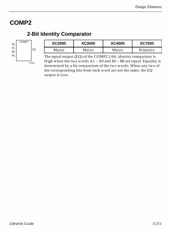
Design Elements
COMP2
2-Bit Identity Comparator
The equal output (EQ) of the COMP2 2-bit, identity comparator isHigh when the two words A1 – A0 and B1 – B0 are equal. Equality isdetermined by a bit comparison of the two words. When any two ofthe corresponding bits from each word are not the same, the EQoutput is Low.
XC2000 XC3000 XC4000 XC7000
Macro Macro Macro PrimitiveEQ
X4122
COMP2A0
A1
B0
B1
Libraries Guide 3-211
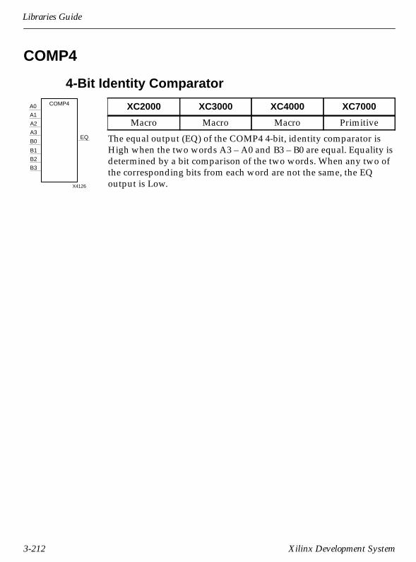
Libraries Guide
COMP4
4-Bit Identity Comparator
The equal output (EQ) of the COMP4 4-bit, identity comparator isHigh when the two words A3 – A0 and B3 – B0 are equal. Equality isdetermined by a bit comparison of the two words. When any two ofthe corresponding bits from each word are not the same, the EQoutput is Low.
XC2000 XC3000 XC4000 XC7000
Macro Macro Macro Primitive
X4126
COMP4
B1
B2
B3
B0
A3
A2
A1
A0
EQ
3-212 Xilinx Development System
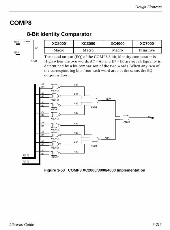
Design Elements
COMP8
8-Bit Identity Comparator
The equal output (EQ) of the COMP8 8-bit, identity comparator isHigh when the two words A7 – A0 and B7 – B0 are equal. Equality isdetermined by a bit comparison of the two words. When any two ofthe corresponding bits from each word are not the same, the EQoutput is Low.
Figure 3-53 COMP8 XC2000/3000/4000 Implementation
XC2000 XC3000 XC4000 XC7000
Macro Macro Macro PrimitiveEQ
A[7:0] COMP8
B[7:0]
X4131
AND2
AND4
AND4
EQ
A1
A0
A2
A3
A4
A5
A6
A7
A[7:0]
AB6
AB5B5
B4
B3
B2
B1
B0
B6
B7
B[7:0]
AB47
AB03
AB0
AB1
AB2
AB3
AB7
AB4
XNOR2
XNOR2
XNOR2
XNOR2
XNOR2
XNOR2
XNOR2
XNOR2
Libraries Guide 3-213

Libraries Guide
COMP16
16-Bit Identity Comparator
The equal output (EQ) of the COMP16 16-bit, identity comparator isHigh when the two words A15 – A0 and B15 – B0 are equal. Equalityis determined by a bit comparison of the two words. When any twoof the corresponding bits from each word are not the same, the EQoutput is Low.
XC2000 XC3000 XC4000 XC7000
Macro Macro Macro Primitive
A[15:0] COMP16
B[15:0]
EQ
X4133
3-214 Xilinx Development System

Design Elements
COMPM2
2-Bit Magnitude Comparator
COMPM2 is a 2-bit, magnitude comparator that compares two posi-tive binary-weighted words A1 – A0 and B1 – B0, where A1 and B1are the most significant bits. The greater-than output (GT) is Highwhen A>B, and the less-than output (LT) is High when A<B. Whenthe two words are equal, both GT and LT are Low. Equality can bemeasured with this macro by comparing both outputs with a NORgate.
XC2000 XC3000 XC4000 XC7000
Macro Macro Macro Primitive
Inputs Outputs
A1 B1 A0 B0 GT LT
0 0 0 0 0 00 0 1 0 1 00 0 0 1 0 10 0 1 1 0 01 1 0 0 0 01 1 1 0 1 01 1 0 1 0 11 1 1 1 0 01 0 X X 1 00 1 X X 0 1
X4123
COMPM2A0
A1
B0
B1
GT
LT
Libraries Guide 3-215

Libraries Guide
COMPM4
4-Bit Magnitude Comparator
* not supported for XC7336 designs
COMPM4 is a 4-bit, magnitude comparator that compares two posi-tive binary-weighted words A3 – A0 and B3 – B0, where A3 and B3are the most significant bits. The greater-than output (GT) is Highwhen A>B, and the less-than output (LT) is High when A<B. Whenthe two words are equal, both GT and LT are Low. Equality can bemeasured with this macro by comparing both outputs with a NORgate.
XC2000 XC3000 XC4000 XC7000
Macro Macro Macro Primitive*
Inputs Outputs
A3, B3 A2, B2 A1, B1 A0, B0 GT LT
A3>B3 X X X 1 0A3<B3 X X X 0 1A3=B3 A2>B2 X X 1 0A3=B3 A2<B2 X X 0 1A3=B3 A2=B2 A1>B1 X 1 0A3=B3 A2=B2 A1<B1 X 0 1A3=B3 A2=A2 A1=B1 A0>B0 1 0A3=B3 A2=B2 A1=B1 A0<B0 0 1A3=B3 A2=B2 A1=B1 A0=B0 0 0
X4127
COMPM4
B1
B2
B3
B0
A3
A2
A1
A0
LT
GT
3-216 Xilinx Development System

Design Elements
COMPM8
8-Bit Magnitude Comparator
* not supported for XC7336 designs
COMPM8 is an 8-bit, magnitude comparator that compares two posi-tive binary-weighted words A7 – A0 and B7 – B0, where A7 and B7are the most significant bits. The greater-than output (GT) is Highwhen A>B, and the less-than output (LT) is High when A<B. Whenthe two words are equal, both GT and LT are Low. Equality can bemeasured with this macro by comparing both outputs with a NORgate. Refer to the “COMPM4” section earlier in this chapter for arepresentative truth table.
XC2000 XC3000 XC4000 XC7000
Macro Macro Macro Primitive*
A[7:0] COMPM8
B[7:0]LT
GT
X4132
Libraries Guide 3-217

Libraries Guide
Figure 3-54 COMPM8 XC2000/3000/4000 Implementation
LTC
GT_7
LT_5
GT_5
GE4_5
LE4_5
GE0_1
LTD
EQ6_7
EQ4_5
GTC
GTB
LTB
GT2_3
LT2_3
LT4_5
GT4_5
GTD
LT_7
GE6_7
LE6_7EQ_7
EQ_5
GT0_1
LT0_1
GT
LT
LTA
LT_1
LE0_1
GT_1
LE2_3
GT_3
LT_3
GE2_3
EQ_3
EQ_1
EQ2_3
GTA
A[7:0] A7
A6
A5
A4
A3
A2
A1
A0
B[7:0] B7
B6
B5
B4
B3
B2
B1
B0
AND2B1
OR4
NOR2
AND3OR2
OR2
OR2
AND3B1
AND3B1
AND3B1
AND3B1
XNOR2
AND2B1
XNOR2
AND2B1
AND2B1
OR2
AND2B1
AND2
AND2
NOR2
OR2
AND2B1
AND2B1
XNOR2
AND2B1
XNOR2
AND3B1
AND3B1
AND3B1
AND3B1
OR2
OR2
OR2
AND4
AND4
AND3
NOR2
OR4
3-218 Xilinx Development System
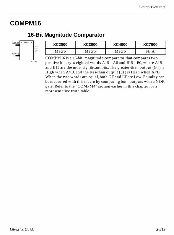
Design Elements
COMPM16
16-Bit Magnitude Comparator
COMPM16 is a 16-bit, magnitude comparator that compares twopositive binary-weighted words A15 – A0 and B15 – B0, where A15and B15 are the most significant bits. The greater-than output (GT) isHigh when A>B, and the less-than output (LT) is High when A<B.When the two words are equal, both GT and LT are Low. Equality canbe measured with this macro by comparing both outputs with a NORgate. Refer to the “COMPM4” section earlier in this chapter for arepresentative truth table.
XC2000 XC3000 XC4000 XC7000
Macro Macro Macro N/A
A[15:0] COMPM16
B[15:0]LT
GT
X4134
Libraries Guide 3-219

Libraries Guide
COMPMC8
8-Bit Magnitude Comparator
COMPMC8 is an 8-bit, magnitude comparator that compares twopositive binary-weighted words A7 – A0 and B7 – B0, where A7 andB7 are the most significant bits. The comparator is implemented usingcarry logic with relative location constraints, which assures most effi-cient logic placement. The greater-than output (GT) is High whenA>B, and the less-than output (LT) is High when A<B. When the twowords are equal, both GT and LT are Low. Equality can be measuredwith this macro by comparing both outputs with a NOR gate. Refer tothe “COMPM4” section earlier in this chapter for a representativetruth table.
XC4000 Topology
In the process of combining the logic that loads GT and LT, the place and routesoftware might map the logic that generates GT and LT to different functiongenerators. If this mapping occurs, the GT and LT logic cannot be placed in theuppermost CLB, as indicated in the illustration.
XC2000 XC3000 XC4000 XC7000
N/A N/A Macro N/A
A[7:0] COMPMC8
B[7:0]LT
GT
X4264
X4341
GT*
LT*
B 7
B 6
B 5
B 4
B 3
B 2
B 1
B 0
A 7
A 6
A 5
A 4
A 3
A 2
A 1
A 0
3-220 Xilinx Development System

Design Elements
Figure 3-55 COMPMC8 XC4000 Implementation
RLOC=R4C0
I1I2I3
O
HMAP
RLOC=R3C0
I1I2I3
O
HMAP
RLOC=R2C0
I1I2I3
O
HMAP
S01
S23
S45
S5
S4
EQ
S7
LT
AND4NOR2
S3
AND2
S5
AND2
S4
A2
A4B4
B2
B1A1
B0A0
B3A3
A5
A6
A7B7
B6
B5
A7
A[7:0]
A0
A1
A2
A3
A4
A5
A6
RLOC=R1C0.G
I1I2I3I4
O
FMAP
XNOR2
XNOR2
XNOR2
XNOR2
CY4_38FORCE-1
INV
RLOC=R3C0.G
I1I2I3I4
O
FMAP
RLOC=R1C0.F
I1I2I3I4
O
FMAP
RLOC=R2C0.G
I1I2I3I4
O
FMAP
RLOC=R2C0.F
I1I2I3I4
O
FMAP
RLOC=R3C0.F
I1I2I3I4
O
FMAP
RLOC=R4C0.G
I1I2I3I4
O
FMAP
SUB-FG-CICY4_07
SUB-FG-CICY4_07
SUB-FG-CICY4_07
CY4_42EXAMINE-CI
RLOC=R5C0
A0ADD
B1A1B0
CY4
CIN
COUTCOUT0
(F3)(F1)(F2)(G4)(G1)
CARRY MODE
RLOC=R4C0
A0ADD
B1A1B0
CY4
CIN
COUTCOUT0
(F3)(F1)(F2)(G4)(G1)
CARRY MODE
RLOC=R0C0
A0ADD
B1A1B0
CY4
CIN
COUTCOUT0
(F3)(F1)(F2)(G4)(G1)
CARRY MODE
RLOC=R2C0
A0ADD
B1A1B0
CY4
CIN
COUTCOUT0
(F3)(F1)(F2)(G4)(G1)
RLOC=R3C0
A0ADD
B1A1B0
CY4
CIN
COUTCOUT0
(F3)(F1)(F2)(G4)(G1)
RLOC=R4C0.F
I1I2I3I4
O
FMAP
RLOC=R1C0
A0ADD
B1A1B0
CY4
CIN
COUTCOUT0
(F3)(F1)(F2)(G4)(G1)
XNOR2
XNOR2
XNOR2
XNOR2
S6
AND2
S2
GT
S3
S2
S1
S0
SUB-FG-CICY4_07
B7
B[7:0]
B0
B1
B2
B3
B4
B5
B6
S45
S23
S67
S1
AND2
S0
S01
RLOC=R1C0
I1I2I3
O
HMAP
S6
S7
S67
C_IN
C2
C4
CO
C6
CARRY MODE
CARRY MODE
CARRY MODE
COMPMC8.4K
Libraries Guide 3-221

Libraries Guide
COMPMC16
16-Bit Magnitude Comparator
COMPMC16 is a 16-bit, magnitude comparator that compares twopositive binary-weighted words A15 – A0 and B15 – B0, where A15and B15 are the most significant bits. The comparator is implementedusing carry logic with relative location constraints, which assuresmost efficient logic placement. The greater-than output (GT) is Highwhen A>B, and the less-than output (LT) is High when A<B. Whenthe two words are equal, both GT and LT are Low. Equality can bemeasured with this macro by comparing both outputs with a NORgate. Refer to the “COMPM4” section earlier in this chapter for arepresentative truth table.
XC2000 XC3000 XC4000 XC7000
N/A N/A Macro N/A
A[15:0] COMPMC16
B[15:0]LT
GT
X4265
3-222 Xilinx Development System

Design Elements
XC4000 Topology
In the process of combining the logic that loads GT and LT, the place and routesoftware might map the logic that generates GT and LT to different functiongenerators. If this mapping occurs, the GT and LT logic cannot be placed in theuppermost CLB, as indicated in the illustration.
X4342
GT*
LT*
B 15
B 14
B 13
B 12
B 11
B 10
B 9
B 8
A 15
A 14
A 13
A 12
A 11
A 10
A 9
A 8
B 7
B 6
B 5
B 4
B 3
B 2
B 1
B 0
A 7
A 6
A 5
A 4
A 3
A 2
A 1
A 0
Libraries Guide 3-223

Libraries Guide
CR8CE
8-Bit Negative-Edge Binary Ripple Counter withClock Enable and Asynchronous Clear
CR8CE is an 8-bit, cascadable, clearable, binary, ripple counter. Theasynchronous clear (CLR), when High, overrides all other inputs andcauses the outputs (Q7 – Q0) to go to logic level zero. The counterincrements when the clock enable input (CE) is High during theHigh-to-Low clock (C) transition. The counter ignores clock transi-tions when CE is Low.
Larger counters can be created by connecting the Q7 output of thefirst stage to the clock input of the next stage. CLR and CE inputs areconnected in parallel. The clock period is not affected by the overalllength of a ripple counter. The overall clock-to-output propagation isn(TC - Q), where n is the number of stages and TC - Q is the C-to-Q7propagation delay of each stage.
The counter is asynchronously reset, output Low, when power isapplied or when global reset (GR for XC2000, XC3000) or globalset/reset (GSR for XC4000) is active. GR is active-Low; the GSR activelevel is programmable. For XC7000, the clock (C) cannot be driven bya FastCLK (BUFG).
XC2000 XC3000 XC4000 XC7000
Macro Macro Macro Primitive
Inputs Outputs
CLR CE C Q7 – Q0
1 X X 00 0 X No Chg0 1 ↓ Inc
X4116
CR8CE
C
CLR
CE
Q[7:0]
3-224 Xilinx Development System

Design Elements
Figure 3-56 CR8CE XC2000/3000/4000 Implementation
CLR
Q5
Q6
Q7
Q4Q0
Q3
Q3
Q2
Q1
Q[7:0]
INVTQ0
C
CE
TQ1
TQ2
TQ3
TQ4
TQ5
TQ6
TQ7
Q3
CECLR
Q
C
D
FDCE_1
Q2
CECLR
Q
C
D
FDCE_1
Q0
CECLR
Q
C
D
FDCE_1
Q1
CECLR
Q
C
D
FDCE_1
Q7
CECLR
Q
C
D
FDCE_1
Q6
CECLR
Q
C
D
FDCE_1
Q5
CECLR
Q
C
D
FDCE_1
Q4
CECLR
Q
C
D
FDCE_1
INV
INV
INV
INVINV
INV
INV
Libraries Guide 3-225

Libraries Guide
CR16CE
16-Bit Negative-Edge Binary Ripple Counter withClock Enable and Asynchronous Clear
CR16CE is a 16-bit, cascadable, clearable, binary, ripple counter. Theasynchronous clear (CLR), when High, overrides all other inputs andcauses the outputs (Q15 – Q0) to go to logic level zero. The counterincrements when the clock enable input (CE) is High during theHigh-to-Low clock (C) transition. The counter ignores clock transi-tions when CE is Low.
Larger counters can be created by connecting the Q15 output of thefirst stage to the clock input of the next stage. CLR and CE inputs areconnected in parallel. The clock period is not affected by the overalllength of a ripple counter. The overall clock-to-output propagation isn(TC - Q), where n is the number of stages and TC - Q is the C-to-Q15propagation delay of each stage.
The counter is asynchronously reset, output Low, when power isapplied or when global reset (GR for XC2000, XC3000) or globalset/reset (GSR for XC4000) is active. GR is active-Low; the GSR activelevel is programmable. For XC7000, the clock (C) cannot be driven bya FastCLK (BUFG).
XC2000 XC3000 XC4000 XC7000
Macro Macro Macro Primitive
Inputs Outputs
CLR CE C Q15 – Q0
1 X X 00 0 X No Chg0 1 ↓ Inc
X4120
CR16CE
C
CLR
CE
Q[15:0]
3-226 Xilinx Development System

Design Elements
D2_4E
2- to 4-Line Decoder/Demultiplexer with Enable
When the enable (EN) input of the D2_4E decoder/demultiplexer isHigh, one of four active-High outputs (D3 – D0) is selected with a2-bit binary address (A1 – A0) input. The non-selected outputs areLow. Also, when the EN input is Low, all outputs are Low. In demul-tiplexer applications, the EN input is the data input.
Figure 3-57 D2_4E XC2000/3000/4000 Implementation
XC2000 XC3000 XC4000 XC7000
Macro Macro Macro Primitive
Inputs Outputs
A1 A0 E D3 D2 D1 D0
X X 0 0 0 0 00 0 1 0 0 0 10 1 1 0 0 1 01 0 1 0 1 0 01 1 1 1 0 0 0
X3853
D2_4E
E
A1
D0
D3
D1
D2
A0
A0
A1
E
AND3B2
D0
D1
D2AND3B1
AND3B1D3
AND3
Libraries Guide 3-227

Libraries Guide
D3_8E
3- to 8-Line Decoder/Demultiplexer with Enable
When the enable (EN) input of the D3_8E decoder/demultiplexer isHigh, one of eight active-High outputs (D7 – D0) is selected with a3-bit binary address (A2 – A0) input. The non-selected outputs areLow. Also, when the EN input is Low, all outputs are Low. In demul-tiplexer applications, the EN input is the data input.
XC2000 XC3000 XC4000 XC7000
Macro Macro Macro Primitive
Inputs Outputs
A2 A1 A0 E D7 D6 D5 D4 D3 D2 D1 D0
X X X 0 0 0 0 0 0 0 0 00 0 0 1 0 0 0 0 0 0 0 10 0 1 1 0 0 0 0 0 0 1 00 1 0 1 0 0 0 0 0 1 0 00 1 1 1 0 0 0 0 1 0 0 01 0 0 1 0 0 0 1 0 0 0 01 0 1 1 0 0 1 0 0 0 0 01 1 0 1 0 1 0 0 0 0 0 01 1 1 1 1 0 0 0 0 0 0 0
X3854
D3_8E
E
D4
D7
D5
D6
A2
A1
A0 D0
D3
D1
D2
3-228 Xilinx Development System

Design Elements
Figure 3-58 D3_8E XC2000/3000/4000 Implementation
D7
D6
D5
D4
D3
D2
D1
D0
D[7:0]
AND4B3
AND4B2
AND4B2
AND4B1
AND4B2
AND4B1
AND4B1
AND4
E
A0
A1
A2
Libraries Guide 3-229

Libraries Guide
D4_16E
4- to 16-Line Decoder/Demultiplexer with Enable
When the enable (EN) input of the D4_16E decoder/demultiplexer isHigh, one of 16 active-High outputs (D15 – D0) is selected with a 4-bitbinary address (A3 – A0) input. The non-selected outputs are Low.Also, when the EN input is Low, all outputs are Low. In demulti-plexer applications, the EN input is the data input. Refer to “D3_8E”for truth table derivation.
XC2000 XC3000 XC4000 XC7000
Macro Macro Macro Primitive
X3855
D4_16E
E
D12
D15
D13
D14
A2
A1
A0
D8
D11
D9
D10
D4
D7
D5
D6
D0
D3
D1
D2
A3
3-230 Xilinx Development System
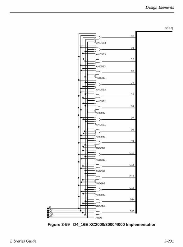
Design Elements
Figure 3-59 D4_16E XC2000/3000/4000 Implementation
AND5B4
AND5B3
AND5B3
AND5B2
AND5B3
AND5B2
AND5B1
AND5B2
AND5
AND5B1
AND5B1
AND5B2
AND5B1
AND5B2
AND5B2
AND5B3
E
A2A3
A1A0
D15
D[15:0]
D0
D1
D2
D3
D4
D5
D6
D7
D8
D9
D10
D11
D12
D13
D14
Libraries Guide 3-231

Libraries Guide
DECODE4, DECODE8, and DECODE 16
4-, 8-, and 16-Bit Active-Low Edge Decoders
These decoders are open-drain wired-AND gates. When one or moreof the inputs (I) are Low, output (O) is Low. When all of the inputs areHigh, the output is High or “Off.” A pull-up resistor must beconnected to the output node to achieve a true logic High. A doublepull-up resistor can be used to achieve faster performance but usesmore power.
The XACT software implements these macros using the open-drainAND gates around the periphery of the XC4000 devices.
Note: Diamonds in library symbols indicate an open-drain output.
A pull-up resistor must be connected to the output to establish High−level drivecurrent.
XC2000 XC3000 XC4000 XC7000
N/A N/A Macro N/A
Inputs Outputs
I0 I1 ... In – 1 O
1 1 1 1 10 X X X 0X 0 X X 0X X X 0 0
X3907
DECODE4
A3
A2
A1
A0
O
X3908
A7
A6
A5
A4
O
DECODE8
A3
A2
A1
A0
X3909
A15
A14
A13
A12
O
DECODE16
A11
A10
A9
A8
A7
A6
A5
A4
A3
A2
A1
A0
3-232 Xilinx Development System
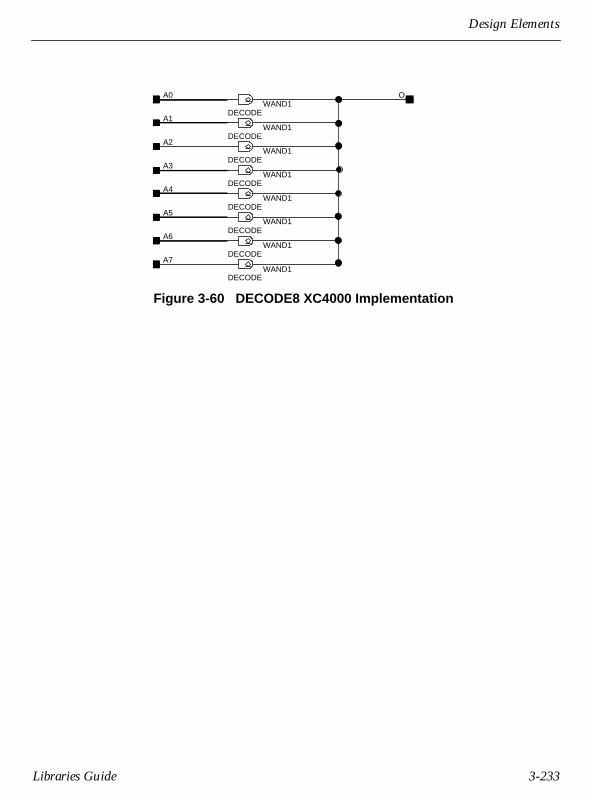
Design Elements
Figure 3-60 DECODE8 XC4000 Implementation
A7
A5
A4
A1
A0
A6
DECODEWAND1
DECODEWAND1
DECODEWAND1
O
DECODEWAND1
DECODEWAND1
DECODEWAND1
DECODEWAND1
DECODEWAND1
A2
A3
Libraries Guide 3-233

Libraries Guide
FD, FD4, FD8, and FD16
Single and Multiple D Flip-Flops
FD is a single D-type flip-flop with data input (D) and data output(Q). FD4, FD8, and FD16 are 4-bit, 8-bit, and 16-bit registers, eachwith a common clock (C). The data on the D inputs is loaded into theflip-flop during the Low-to-High clock (C) transition.
The flip-flop is asynchronously reset, output Low, when power isapplied or when global reset (GR for XC2000, XC3000) or globalset/reset (GSR for XC4000) is active. GR is active-Low; the GSR activelevel is programmable.
Figure 3-61 FD XC2000 Implementation
Element XC2000 XC3000 XC4000 XC7000
FD Macro Macro Macro PrimitiveFD4,FD8,FD16
N/A N/A N/A Primitive
Inputs Outputs
D C Q
0 ↑ 01 ↑ 1
Q
X3715
D FD
C
Q0
X4608
D0 FD4
C
Q1D1
Q2D2
Q3D3
Q[7:0]D[7:0]
X4609
FD8
C
Q[15:0]D[15:0]
X4610
FD16
C
C
Q
GND
D
CCLR
DPRE
Q
FDCP
3-234 Xilinx Development System

Design Elements
Figure 3-62 FD XC3000/4000 Implementation
FDCE
QD
CLR
CEC
D
VCC
C
Q
GND
Libraries Guide 3-235

Libraries Guide
FD_1
D Flip-Flop with Negative-Edge Clock
FD_1 is a single D-type flip-flop with data input (D) and data output(Q). The data on the D input is loaded into the flip-flop during theHigh-to-Low clock (C) transition.
The flip-flop is asynchronously reset, output Low, when power isapplied or when global reset (GR for XC2000, XC3000) or globalset/reset (GSR for XC4000) is active. GR is active-Low; the GSR activelevel is programmable.
Figure 3-63 FD_1 XC2000 Implementation
Figure 3-64 FD_1 XC3000/4000 Implementation
XC2000 XC3000 XC4000 XC7000
Macro Macro Macro N/A
Inputs Outputs
D C Q
0 ↓ 01 ↓ 1
Q
X3726
D FD_1
C
CBC
GND
QD
INVC
CLR
D PRE Q
FDCP
CBC
GND
Q
VCC
DFDCE
QD
CLR
CEC
INV
3-236 Xilinx Development System

Design Elements
FD4CE
4-Bit Data Register with Clock Enable andAsynchronous Clear
When clock enable (CE) is High, and asynchronous clear (CLR) isLow, the data on the four data inputs (D3 – D0) of FD4CE is trans-ferred to the corresponding data outputs (Q3 – Q0) during the Low-to-High clock (C) transition. When CLR is High, it overrides all otherinputs and resets the data outputs (Q3 – Q0) Low. When CE is Low,clock transitions are ignored.
The flip-flops are asynchronously reset, outputs Low, when power isapplied or when global reset (GR for XC2000, XC3000) or globalset/reset (GSR for XC4000) is active. GR is active-Low; the GSR activelevel is programmable.
dn = state of corresponding input one set-up time prior to active clock transition
XC2000 XC3000 XC4000 XC7000
Macro Macro Macro Primitive
Inputs Outputs
CLR CE D3 – D0 C Q3 – Q0
1 X X X 00 0 X X No Chg0 1 Dn ↑ dn
X3733
FD4CE
C
CE
D3D2
D1
D0
CLR
Q3Q2
Q1
Q0
Libraries Guide 3-237
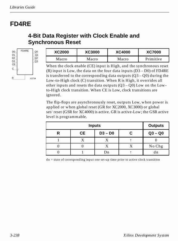
Libraries Guide
FD4RE
4-Bit Data Register with Clock Enable andSynchronous Reset
When the clock enable (CE) input is High, and the synchronous reset(R) input is Low, the data on the four data inputs (D3 – D0) of FD4REis transferred to the corresponding data outputs (Q3 – Q0) during theLow-to-High clock (C) transition. When R is High, it overrides allother inputs and resets the data outputs (Q3 – Q0) Low on the Low-to-High clock transition. When CE is Low, clock transitions areignored.
The flip-flops are asynchronously reset, outputs Low, when power isapplied or when global reset (GR for XC2000, XC3000) or globalset/reset (GSR for XC4000) is active. GR is active-Low; the GSR activelevel is programmable.
dn = state of corresponding input one set-up time prior to active clock transition
XC2000 XC3000 XC4000 XC7000
Macro Macro Macro Primitive
Inputs Outputs
R CE D3 – D0 C Q3 – Q0
1 X X ↑ 00 0 X X No Chg0 1 Dn ↑ dn
X3734
D3
FD4RE
C
R
D2D1D0
Q3Q2Q1Q0
CE
3-238 Xilinx Development System
Design Elements
FD8CE
8-Bit Data Register with Clock Enable andAsynchronous Clear
When clock enable (CE) is High, and asynchronous clear (CLR) isLow, the data on the eight data inputs (D7 – D0) of FD8CE is trans-ferred to the corresponding data outputs (Q7 – Q0) during the Low-to-High clock (C) transition. When CLR is High, it overrides all otherinputs and resets the data outputs (Q7 – Q0) Low. When CE is Low,clock transitions are ignored.
The flip-flops are asynchronously reset, outputs Low, when power isapplied or when global reset (GR for XC2000, XC3000) or globalset/reset (GSR for XC4000) is active. GR is active-Low; the GSR activelevel is programmable.
dn = state of corresponding input one set-up time prior to active clock transition
XC2000 XC3000 XC4000 XC7000
Macro Macro Macro Primitive
Inputs Outputs
CLR CE D7 – D0 C Q7 – Q0
1 X X X 00 0 X X No Chg0 1 Dn ↑ dn
X3850
FD8CE
C
CLR
CE
D[7:0] Q[7:0]
Libraries Guide 3-239
Libraries Guide
Figure 3-65 FD8CE XC2000/3000/4000 Implementation
Q7
FDCEQD
CLR
CEC
Q6
FDCEQD
CLR
CEC
Q4
FDCEQD
CLR
CEC
Q5
FDCEQD
CLR
CEC
Q0
FDCEQD
CLR
CEC
Q[7:0]
Q3
Q2
Q1
Q0
Q7
Q6
Q5
Q4
CECCLR
D[7:0]
D0
D1
D2
D3 D7
D6
D5
D4
Q1
FDCEQD
CLR
CEC
Q2
FDCEQD
CLR
CEC
Q3
FDCE
QD
CLR
CEC
3-240 Xilinx Development System

Design Elements
FD8RE
8-Bit Data Register with Clock Enable andSynchronous Reset
When the clock enable (CE) input is High, and the synchronous reset(R) input is Low, the data on the eight data inputs (D7 – D0) of FD8REis transferred to the corresponding data outputs (Q7 – Q0) during theLow-to-High clock (C) transition. When R is High, it overrides allother inputs and resets the data outputs (Q7 – Q0) Low on the Low-to-High clock transition. When CE is Low, clock transitions areignored.
The flip-flops are asynchronously reset, outputs Low, when power isapplied or when global reset (GR for XC2000, XC3000) or globalset/reset (GSR for XC4000) is active. GR is active-Low; the GSR activelevel is programmable.
dn = state of corresponding input one set-up time prior to active clock transition
XC2000 XC3000 XC4000 XC7000
Macro Macro Macro Primitive
Inputs Outputs
R CE D7 – D0 C Q7 – Q0
1 X X ↑ 00 0 X X No Chg0 1 Dn ↑ dn
X3735
FD8RE
C
R
CE
D[7:0] Q[7:0]
Libraries Guide 3-241

Libraries Guide
Figure 3-66 FD8RE XC2000/3000/4000 Implementation
Q7
FDRE
R
QDCEC
R
Q2
FDRE
R
QDCEC
Q6
FDRE
R
QDCEC
Q4
FDRE
R
QDCEC
CEC
Q4
Q[7:0]
Q3
Q2
Q1
Q0
Q7
Q6
Q5
Q0
FDRE
R
QDCEC
Q1
FDRE
R
QDCEC
Q3
FDRE
R
QDCEC
D[7:0]
D5
D6
D7D3
D2
D1
D0 D4
Q5
FDRE
R
QDCEC
3-242 Xilinx Development System

Design Elements
FD16CE
16-Bit Data Register with Clock Enable andAsynchronous Clear
When clock enable (CE) is High, and asynchronous clear (CLR) isLow, the data on the 16 data inputs (D15 – D0) of FD16CE is trans-ferred to the corresponding data outputs (Q15 – Q0) during the Low-to-High clock (C) transition. When CLR is High, it overrides all otherinputs and resets the data outputs (Q15 – Q0) Low. When CE is Low,clock transitions are ignored.
The flip-flops are asynchronously reset, outputs Low, when power isapplied or when global reset (GR for XC2000, XC3000) or globalset/reset (GSR for XC4000) is active. GR is active-Low; the GSR activelevel is programmable.
dn = state of corresponding input one set-up time prior to active clock transition
XC2000 XC3000 XC4000 XC7000
Macro Macro Macro Primitive
Inputs Outputs
CLR CE D15 – D0 C Q15 – Q0
1 X X X 00 0 X X No Chg0 1 Dn ↑ dn
X3736
FD16CE
C
CLR
CE
D[15:0] Q[15:0]
Libraries Guide 3-243
Libraries Guide
FD16RE
16-Bit Data Register with Clock Enable andSynchronous Reset
When the clock enable (CE) input is High, and the synchronous reset(R) input is Low, the data on the 16 data inputs (D15 – D0) of FD16REis transferred to the corresponding data outputs (Q15 – Q0) duringthe Low-to-High clock (C) transition. When R is High, it overrides allother inputs and resets the data outputs (Q15 – Q0) Low on the Low-to-High clock transition. When CE is Low, clock transitions areignored.
The flip-flops are asynchronously reset, outputs Low, when power isapplied or when global reset (GR for XC2000, XC3000) or globalset/reset (GSR for XC4000) is active. GR is active-Low; the GSR activelevel is programmable.
dn = state of corresponding input one set-up time prior to active clock transition
XC2000 XC3000 XC4000 XC7000
Macro Macro Macro Primitive
Inputs Outputs
R CE D15 – D0 C Q15 – Q0
1 X X ↑ 00 0 X X No Chg0 1 Dn ↑ dn
X3737
C
R
CE
D[15:0] Q[15:0]FD16RE
3-244 Xilinx Development System
Design Elements
FDC
D Flip-Flop with Asynchronous Clear
FDC is a single D-type flip-flop with data (D) and asynchronous clear(CLR) inputs and data output (Q). The asynchronous CLR, whenHigh, overrides all other inputs and sets the Q output Low. The dataon the D input is loaded into the flip-flop when CLR is Low on theLow-to-High clock transition.
The flip-flop is asynchronously reset, output Low, when power isapplied or when global reset (GR for XC2000, XC3000) or globalset/reset (GSR for XC4000) is active. GR is active-Low; the GSR activelevel is programmable.
Figure 3-67 FDC XC2000 Implementation
Figure 3-68 FDC XC3000/4000 Implementation
XC2000 XC3000 XC4000 XC7000
Macro Macro Macro Primitive
Inputs Outputs
CLR D C Q
1 X X 00 1 ↑ 10 0 ↑ 0
X3716CLR
C
QDFDC
GND
CLR
C
QD
CCLR
D PRE Q
FDCP
CLR
C
VCC
QD
FDCEQD
CLR
CEC
Libraries Guide 3-245

Libraries Guide
FDC_1
D Flip-Flop with Negative-Edge Clock andAsynchronous Clear
FDC_1 is a single D-type flip-flop with data input (D), asynchronousclear input (CLR) and data output (Q). The asynchronous CLR, whenactive, overrides all other inputs and sets the Q output Low. The dataon the D input is loaded into the flip-flop during the High-to-Lowclock (C) transition.
The flip-flop is asynchronously reset, output Low, when power isapplied or when global reset (GR for XC2000, XC3000) or globalset/reset (GSR for XC4000) is active. GR is active-Low; the GSR activelevel is programmable.
Figure 3-69 FDC_1 XC2000 Implementation
XC2000 XC3000 XC4000 XC7000
Macro Macro Macro N/A
Inputs Outputs
CLR D C Q
1 X X 00 1 ↓ 10 0 ↓ 0
Q
X3847
D FDC_1
C
CLR
CBCINV
Q
CLR
D
GND
CCLR
D PRE Q
FDCP
3-246 Xilinx Development System

Design Elements
Figure 3-70 FDC_1 XC3000/4000 Implementation
CBC
INV
FDCE
QD
CLR
CEC
Q
VCC
CLR
D
Libraries Guide 3-247
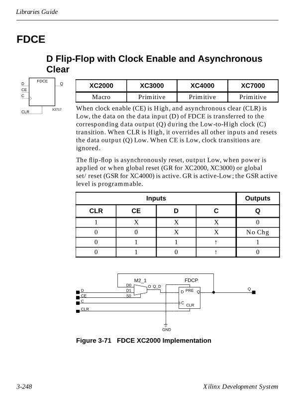
Libraries Guide
FDCE
D Flip-Flop with Clock Enable and AsynchronousClear
When clock enable (CE) is High, and asynchronous clear (CLR) isLow, the data on the data input (D) of FDCE is transferred to thecorresponding data output (Q) during the Low-to-High clock (C)transition. When CLR is High, it overrides all other inputs and resetsthe data output (Q) Low. When CE is Low, clock transitions areignored.
The flip-flop is asynchronously reset, output Low, when power isapplied or when global reset (GR for XC2000, XC3000) or globalset/reset (GSR for XC4000) is active. GR is active-Low; the GSR activelevel is programmable.
Figure 3-71 FDCE XC2000 Implementation
XC2000 XC3000 XC4000 XC7000
Macro Primitive Primitive Primitive
Inputs Outputs
CLR CE D C Q
1 X X X 00 0 X X No Chg0 1 1 ↑ 10 1 0 ↑ 0
X3717CLR
C
CE
QDFDCE
Q
CEC
DQ_D
CLR
GND
D0D1
O
S0
M2_1
CCLR
D PRE Q
FDCP
3-248 Xilinx Development System

Design Elements
FDCE_1
D Flip-Flop with Negative-Edge Clock, Clock Enable,and Asynchronous Clear
FDCE_1 is a single D-type flip-flop with data (D), clock enable (CE),and asynchronous clear (CLR) inputs and data output (Q). The asyn-chronous CLR input, when High, overrides all other inputs and setsthe Q output Low. The data on the D input is loaded into the flip-flopwhen CLR is Low and CE is High on the High-to-Low clock (C) tran-sition. When CE is Low, the clock transitions are ignored.
The flip-flop is asynchronously reset, output Low, when power isapplied or when global reset (GR for XC2000, XC3000) or globalset/reset (GSR for XC4000) is active. GR is active-Low; the GSR activelevel is programmable.
XC2000 XC3000 XC4000 XC7000
Macro Macro Macro N/A
Inputs Outputs
CLR CE D C Q
1 X X X 00 0 X ↓ No Chg0 1 1 ↓ 10 1 0 ↓ 0
Q
X3727
D FDCE_1
C
CLR
CE
Libraries Guide 3-249

Libraries Guide
Figure 3-72 FDCE_1 XC2000 Implementation
Figure 3-73 FDCE_1 XC3000/4000 Implementation
CB
D0D1
O
S0
M2_1
GND
CLR
Q_DDCE
Q
INV
C CCLR
D PRE Q
FDCP
CB
CLR
QFDCE
QD
CLR
CEC
INV
C
DCE
3-250 Xilinx Development System

Design Elements
FDCP
D Flip-Flop with Asynchronous Preset and Clear
* not supported for XC7336 designs
FDCP is a single D-type flip-flop with data (D), asynchronous preset(PRE) and clear (CLR) inputs, and data output (Q). The asynchronousPRE, when High, sets the Q output High; CLR, when High, resets theoutput Low. When both PRE and CLR are active, the flip-flop iscleared. Data on the D input is loaded into the flip-flop when PREand CLR are Low on the Low-to-High clock (C) transition.
The flip-flop is asynchronously reset, output Low, when power isapplied or when global reset (GR) is active (Low).
XC2000 XC3000 XC4000 XC7000
Primitive N/A N/A Primitive*
Inputs Outputs
CLR PRE D C Q
1 X X X 00 1 X X 10 0 0 ↑ 00 0 1 ↑ 1
Q
D
C
FDCP
PRE
CLR X4397
Libraries Guide 3-251

Libraries Guide
FDCPE
D Flip-Flop with Clock Enable and AsynchronousPreset and Clear
* not supported for XC7336 designs
FDCPE is a single D-type flip-flop with data (D), clock enable (CE),asynchronous preset (PRE), and asynchronous clear (CLR) inputs anddata output (Q). The asynchronous PRE, when High, sets the Qoutput High; CLR, when High, resets the output Low. When bothPRE and CLR are active, the flip-flop is cleared. Data on the D input isloaded into the flip-flop when PRE and CLR are Low and CE is Highon the Low-to-High clock (C) transition. When CE is Low, the clocktransitions are ignored.
The flip-flop is asynchronously reset, output Low, when power isapplied or when global reset (GR) is active (Low).
XC2000 XC3000 XC4000 XC7000
Macro N/A N/A Primitive*
Inputs Outputs
CLR PRE CE D C Q
1 X X X X 00 1 X X X 10 0 0 X X No Chg0 0 1 0 ↑ 00 0 1 1 ↑ 1
Q
D
C
FDCPE
CE
PRE
CLR X4389
3-252 Xilinx Development System

Design Elements
Figure 3-74 FDCPE XC2000 Implementation
PRECE
Q
D0D1
O
S0
M2_1
CCLR
DPRE
Q
FDCP
CLR
Q_DD
C
Libraries Guide 3-253

Libraries Guide
FDP
D Flip-Flop with Asynchronous Preset
FDP is a single D-type flip-flop with data (D) and asynchronouspreset (PRE) inputs, and data output (Q). The asynchronous PRE,when High, overrides all other inputs and presets the Q output High.The data on the D input is loaded into the flip-flop when PRE is Lowon the Low-to-High clock (C) transition. The flip-flop is asynchro-nously set, output High, when global set/reset (GSR) is active; theGSR active level is programmable.
Figure 3-75 FDP XC4000 Implementation
XC2000 XC3000 XC4000 XC7000
N/A N/A Macro Primitive
Inputs Outputs
PRE C D Q
1 X X 10 ↑ 1 10 ↑ 0 0
Q
X3720
DFDP
C
PRE
VCC
C
CE
DPRE
Q
FDPE
C
QD
PRE
3-254 Xilinx Development System
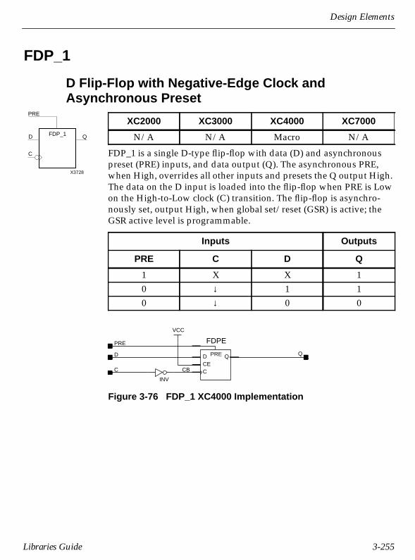
Design Elements
FDP_1
D Flip-Flop with Negative-Edge Clock andAsynchronous Preset
FDP_1 is a single D-type flip-flop with data (D) and asynchronouspreset (PRE) inputs, and data output (Q). The asynchronous PRE,when High, overrides all other inputs and presets the Q output High.The data on the D input is loaded into the flip-flop when PRE is Lowon the High-to-Low clock (C) transition. The flip-flop is asynchro-nously set, output High, when global set/reset (GSR) is active; theGSR active level is programmable.
Figure 3-76 FDP_1 XC4000 Implementation
XC2000 XC3000 XC4000 XC7000
N/A N/A Macro N/A
Inputs Outputs
PRE C D Q
1 X X 10 ↓ 1 10 ↓ 0 0
Q
X3728
D FDP_1
C
PRE
CBC
INV
Q
CCED PRE Q
FDPE
VCC
D
PRE
Libraries Guide 3-255

Libraries Guide
FDPE
D Flip-Flop with Clock Enable and AsynchronousPreset
FDPE is a single D-type flip-flop with data (D), clock enable (CE), andasynchronous preset (PRE) inputs and data output (Q). The asynchro-nous PRE, when High, overrides all other inputs and sets the Qoutput High. Data on the D input is loaded into the flip-flop whenPRE is Low and CE is High on the Low-to-High clock (C) transition.When CE is Low, the clock transitions are ignored. The flip-flop isasynchronously set, output High, when global set/reset (GSR) isactive; the GSR active level is programmable.
XC2000 XC3000 XC4000 XC7000
N/A N/A Primitive Primitive
Inputs Outputs
PRE CE D C Q
1 X X X 10 0 X X No Chg0 1 0 ↑ 00 1 1 ↑ 1
X3721
FDPE
C
CE
QD
PRE
3-256 Xilinx Development System
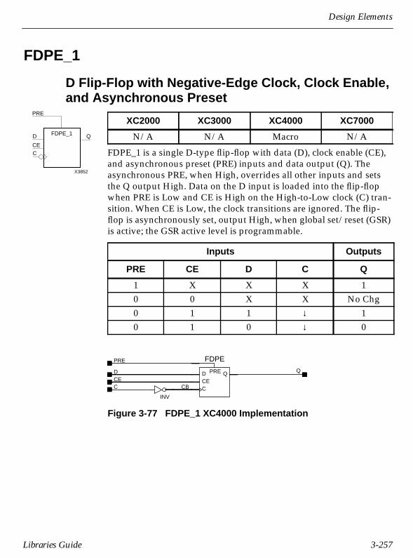
Design Elements
FDPE_1
D Flip-Flop with Negative-Edge Clock, Clock Enable,and Asynchronous Preset
FDPE_1 is a single D-type flip-flop with data (D), clock enable (CE),and asynchronous preset (PRE) inputs and data output (Q). Theasynchronous PRE, when High, overrides all other inputs and setsthe Q output High. Data on the D input is loaded into the flip-flopwhen PRE is Low and CE is High on the High-to-Low clock (C) tran-sition. When CE is Low, the clock transitions are ignored. The flip-flop is asynchronously set, output High, when global set/reset (GSR)is active; the GSR active level is programmable.
Figure 3-77 FDPE_1 XC4000 Implementation
XC2000 XC3000 XC4000 XC7000
N/A N/A Macro N/A
Inputs Outputs
PRE CE D C Q
1 X X X 10 0 X X No Chg0 1 1 ↓ 10 1 0 ↓ 0
Q
X3852
D FDPE_1
C
PRE
CE
PRE
CCED PRE Q
FDPE
Q
INV
C CB
DCE
Libraries Guide 3-257

Libraries Guide
FDR
D Flip-Flop with Synchronous Reset
FDR is a single D-type flip-flop with data (D) and synchronous reset(R) inputs and data output (Q). The synchronous reset (R) input,when High, overrides all other inputs and resets the Q output Low onthe Low-to-High clock (C) transition. The data on the D input isloaded into the flip-flop when R is Low during the Low-to-High clocktransition.
The flip-flop is asynchronously reset, output Low, when power isapplied or when global reset (GR for XC2000, XC3000) or globalset/reset (GSR for XC4000) is active. GR is active-Low; the GSR activelevel is programmable.
Figure 3-78 FDR XC2000/3000/4000 Implementation
XC2000 XC3000 XC4000 XC7000
Macro Macro Macro Primitive
Inputs Outputs
R D C Q
1 X ↑ 00 1 ↑ 10 0 ↑ 0
Q
X3718
D
R
C
FDR
D_R
C
DQ
C
D Q
FD
AND2B1
R
3-258 Xilinx Development System

Design Elements
FDRE
D Flip-Flop with Clock Enable and SynchronousReset
FDRE is a single D-type flip-flop with data (D), clock enable (CE), andsynchronous reset (R) inputs and data output (Q). The synchronousreset (R) input, when High, overrides all other inputs and resets the Qoutput Low on the Low-to-High clock (C) transition. The data on theD input is loaded into the flip-flop when R is Low and CE is Highduring the Low-to-High clock transition.
The flip-flop is asynchronously reset, output Low, when power isapplied or when global reset (GR for XC2000, XC3000) or globalset/reset (GSR for XC4000) is active. GR is active-Low; the GSR activelevel is programmable.
Figure 3-79 FDRE XC2000/3000/4000 Implementation
XC2000 XC3000 XC4000 XC7000
Macro Macro Macro Primitive
Inputs Outputs
R CE D C Q
1 X X ↑ 00 0 X X No Chg0 1 1 ↑ 10 1 0 ↑ 0
X3719
FDRE
C
CE
QD
R
QD
C
D Q
FDD
CE
C
A0A1
QAND3B1
AND3B2 OR2
R
Libraries Guide 3-259

Libraries Guide
FDRS
D Flip-Flop with Synchronous Reset andSynchronous Set
FDRS is a single D-type flip-flop with data (D), synchronous set (S),and synchronous reset (R) inputs and data output (Q). The synchro-nous reset (R) input, when High, overrides all other inputs and resetsthe Q output Low during the Low-to-High clock (C) transition. (Resethas precedence over Set.) When S is High and R is Low, the flip-flop isset, output High, during the Low-to-High clock transition. When Rand S are Low, data on the (D) input is loaded into the flip-flopduring the Low-to-High clock transition.
The flip-flop is asynchronously reset, output Low, when power isapplied or when global reset (GR for XC2000, XC3000) or globalset/reset (GSR for XC4000) is active. GR is active-Low; the GSR activelevel is programmable.
Figure 3-80 FDRS XC2000/3000/4000 Implementation
XC2000 XC3000 XC4000 XC7000
Macro Macro Macro Primitive
Inputs Outputs
R S D C Q
1 X X ↑ 00 1 X ↑ 10 0 1 ↑ 10 0 0 ↑ 0
Q
X3731
DFDRS
C
S
R
R
SD
OR2
Q
C
D_SFDR
R
QD
C
3-260 Xilinx Development System

Design Elements
FDRSE
D Flip-Flop with Synchronous Reset and Set andClock Enable
FDRSE is a single D-type flip-flop with synchronous reset (R),synchronous set (S), and clock enable (CE) inputs and data output(Q). The reset (R) input, when High, overrides all other inputs andresets the Q output Low during the Low-to-High clock transition.(Reset has precedence over Set.) When the set (S) input is High and Ris Low, the flip-flop is set, output High, during the Low-to-High clock(C) transition. Data on the D input is loaded into the flip-flop when Rand S are Low and CE is High during the Low-to-High clock transi-tion.
The flip-flop is asynchronously reset, output Low, when power isapplied or when global reset (GR for XC2000, XC3000) or globalset/reset (GSR for XC4000) is active. GR is active-Low; the GSR activelevel is programmable.
Figure 3-81 FDRSE XC2000/3000/4000 Implementation
XC2000 XC3000 XC4000 XC7000
Macro Macro Macro Primitive
Inputs Outputs
R S CE D C Q
1 X X X ↑ 00 1 X X ↑ 10 0 0 X X No Chg0 0 1 1 ↑ 10 0 1 0 ↑ 0
X3732
FDRSE
C
CE
QD
R
S
SD
CE
FDRE
R
QDCEC
Q
OR2
OR2
C
R
CE_S
D_S
Libraries Guide 3-261

Libraries Guide
FDS
D Flip-Flop with Synchronous Set
FDS is a single D-type flip-flop with data (D) and synchronous set (S)inputs and data output (Q). The synchronous set input, when High,sets the Q output High on the Low-to-high clock (C) transition. Thedata on the D input is loaded into the flip-flop when S is Low duringthe Low-to-High clock (C) transition.
The flip-flop is asynchronously reset, output Low, when power isapplied or when global reset (GR for XC2000, XC3000) or globalset/reset (GSR for XC4000) is active. GR is active-Low; the GSR activelevel is programmable.
Figure 3-82 FDS XC2000/3000/4000 Implementation
XC2000 XC3000 XC4000 XC7000
Macro Macro Macro Primitive
Inputs Outputs
S D C Q
1 X ↑ 10 1 ↑ 10 0 ↑ 0
Q
X3722
D FDS
C
S
C
D Q
FDQ
DS
OR2C
D_S
3-262 Xilinx Development System

Design Elements
FDSE
D Flip-Flop with Clock Enable and Synchronous Set
FDSE is a single D-type flip-flop with data (D), clock enable (CE), andsynchronous set (S) inputs and data output (Q). The synchronous set(S) input, when High, overrides the clock enable (CE) input and setsthe Q output High during the Low-to-High clock (C) transition. Thedata on the D input is loaded into the flip-flop when S is Low and CEis High during the Low-to-High clock (C) transition.
The flip-flop is asynchronously reset, output Low, when power isapplied or when global reset (GR for XC2000, XC3000) or globalset/reset (GSR for XC4000) is active. GR is active-Low; the GSR activelevel is programmable.
Figure 3-83 FDSE XC2000/3000/4000 Implementation
XC2000 XC3000 XC4000 XC7000
Macro Macro Macro Primitive
Inputs Outputs
S CE D C Q
1 X X ↑ 10 0 X X No Chg0 1 1 ↑ 10 1 0 ↑ 0
X3723
FDSE
C
CE
QD
S
CE
Q
A1
C
A0S
DAND2
AND2B1
C
D Q
FDOR3
A_S
Libraries Guide 3-263

Libraries Guide
FDSR
D Flip-Flop with Synchronous Set and Reset
FDSR is a single D-type flip-flop with data (D), synchronous reset (R)and synchronous set (S) inputs and data output (Q). When the set (S)input is High, it overrides all other inputs and sets the Q output Highduring the Low-to-High clock transition. (Set has precedence overReset.) When reset (R) is High and S is Low, the flip-flop is reset,output Low, on the Low-to-High clock transition. Data on the D inputis loaded into the flip-flop when S and R are Low on the Low-to-Highclock transition.
The flip-flop is asynchronously reset, output Low, when power isapplied or when global reset (GR for XC2000, XC3000) or globalset/reset (GSR for XC4000) is active. GR is active-Low; the GSR activelevel is programmable.
Figure 3-84 FDSR XC2000/3000/4000 Implementation
XC2000 XC3000 XC4000 XC7000
Macro Macro Macro Primitive
Inputs Outputs
S R D C Q
1 X X ↑ 10 1 X ↑ 00 0 1 ↑ 10 0 0 ↑ 0
X3729
FDSR
C
QD
R
S
AND2B1C
D QS
FDS
C
QRDS
D_R
3-264 Xilinx Development System

Design Elements
FDSRE
D Flip-Flop with Synchronous Set and Reset andClock Enable
FDSRE is a single D-type flip-flop with synchronous set (S), synchro-nous reset (R), and clock enable (CE) inputs and data output (Q).When synchronous set (S) is High, it overrides all other inputs andsets the Q output High during the Low-to-High clock transition. (Sethas precedence over Reset.) When synchronous reset (R) is High andS is Low, output Q is reset Low during the Low-to-High clock transi-tion. Data is loaded into the flip-flop when S and R are Low and CE isHigh during the Low-to-high clock transition. When CE is Low, clocktransitions are ignored.
The flip-flop is asynchronously reset, output Low, when power isapplied or when global reset (GR for XC2000, XC3000) or globalset/reset (GSR for XC4000) is active. GR is active-Low; the GSR activelevel is programmable.
Figure 3-85 FDSRE XC2000/3000/4000 Implementation
XC2000 XC3000 XC4000 XC7000
Macro Macro Macro Primitive
Inputs Outputs
S R CE D C Q
1 X X X ↑ 10 1 X X ↑ 00 0 0 X X No Chg0 0 1 1 ↑ 10 0 1 0 ↑ 0
X3730
FDSRE
C
CE
QD
R
S
QD_R
AND2B1
FDSES
QDCEC
CE_R
DR
C
S
OR2CE
Libraries Guide 3-265

Libraries Guide
FJKC
J-K Flip-Flop with Asynchronous Clear
FJKC is a single J-K-type flip-flop with J, K, and asynchronous clear(CLR) inputs and data output (Q). The asynchronous clear (CLR)input, when High, overrides all other inputs and resets the Q outputLow. When CLR is Low, the output responds to the state of the J andK inputs, as shown in the following truth table, during the Low-to-High clock (C) transition.
The flip-flop is asynchronously reset, output Low, when power isapplied or when global reset (GR for XC2000, XC3000) or globalset/reset (GSR for XC4000) is active. GR is active-Low; the GSR activelevel is programmable.
Figure 3-86 FJKC XC2000/3000/4000 Implementation
XC2000 XC3000 XC4000 XC7000
Macro Macro Macro Primitive
Inputs Outputs
CLR J K C Q
1 X X X 00 0 0 ↑ No Chg0 0 1 ↑ 00 1 0 ↑ 10 1 1 ↑ Toggle
Q
X3753
J
CLR
C
FJKC
K
Q
AND2B1
OR3AND3B1
AND3B2
A1A0
KJ
A2
C
CLR
AD
QD
CLRC
FDC
3-266 Xilinx Development System

Design Elements
FJKCE
J-K Flip-Flop with Clock Enable and AsynchronousClear
FJKCE is a single J-K-type flip-flop with J, K, clock enable (CE), andasynchronous clear (CLR) inputs and data output (Q). The asynchro-nous clear (CLR), when High, overrides all other inputs and resetsthe Q output Low during the Low-to-High clock (C) transition. WhenCLR is Low and CE is High, Q responds to the state of the J and Kinputs, as shown in the following truth table, during the Low-to-High clock transition. When CE is Low, the clock transitions areignored.
The flip-flop is asynchronously reset, output Low, when power isapplied or when global reset (GR for XC2000, XC3000) or globalset/reset (GSR for XC4000) is active. GR is active-Low; the GSR activelevel is programmable.
XC2000 XC3000 XC4000 XC7000
Macro Macro Macro Primitive
Inputs Outputs
CLR CE J K C Q
1 X X X X 00 0 X X X No Chg0 1 0 0 X No Chg0 1 0 1 ↑ 00 1 1 0 ↑ 10 1 1 1 ↑ Toggle
Q
X3756
J
CLR
C
FJKCE
K
CE
Libraries Guide 3-267

Libraries Guide
Figure 3-87 FJKCE XC2000/3000/4000 Implementation
ADA2
CLR
J
CE
K
C
A0A1
Q
FDCE
QD
CLR
CEC
AND3B2
AND3B1 OR3
AND2B1
3-268 Xilinx Development System

Design Elements
FJKCP
J-K Flip-Flop with Asynchronous Clear and Preset
* not supported for XC7336 designs
FJKCP is a single J-K-type flip-flop with J, K, asynchronous clear(CLR), and asynchronous preset (PRE) inputs and data output (Q).The asynchronous clear input (CLR), when High, overrides all otherinputs and resets the Q output Low on the High-to-Low clock (C)transition. The asynchronous preset (PRE) input, when High(provided CLR is Low), overrides all other inputs and sets the Qoutput High on the Low-to-High clock (C) transition. When CLR andPRE are Low, Q responds to the state of the J and K inputs during theLow-to-High clock transition, as shown in the following truth table.
The flip-flop is asynchronously reset, output Low, when power isapplied or when global reset (GR) is active (Low).
XC2000 XC3000 XC4000 XC7000
Macro N/A N/A Primitive*
Inputs Outputs
CLR PRE J K C Q
1 X X X X 00 1 X X X 10 0 0 0 X No Chg0 0 0 1 ↑ 00 0 1 0 ↑ 10 0 1 1 ↑ Toggle
Q
J
C
FJKCP
K
PRE
CLR X4390
Libraries Guide 3-269
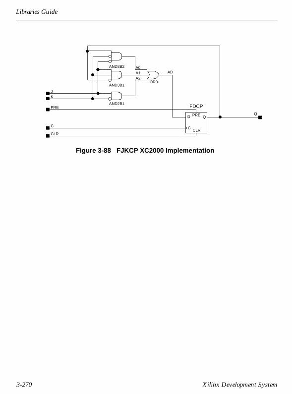
Libraries Guide
Figure 3-88 FJKCP XC2000 Implementation
CLR
PREAND2B1
OR3AND3B1
AND3B2
A1A0
C
A2
AD
Q
KJ
CCLR
D PRE Q
FDCP
3-270 Xilinx Development System
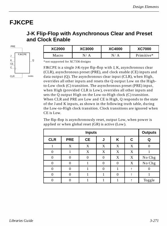
Design Elements
FJKCPE
J-K Flip-Flop with Asynchronous Clear and Presetand Clock Enable
* not supported for XC7336 designs
FJKCPE is a single J-K-type flip-flop with J, K, asynchronous clear(CLR), asynchronous preset (PRE), and clock enable (CE) inputs anddata output (Q). The asynchronous clear input (CLR), when High,overrides all other inputs and resets the Q output Low on the High-to-Low clock (C) transition. The asynchronous preset (PRE) input,when High (provided CLR is Low), overrides all other inputs andsets the Q output High on the Low-to-High clock (C) transition.When CLR and PRE are Low and CE is High, Q responds to the stateof the J and K inputs, as shown in the following truth table, duringthe Low-to-High clock transition. Clock transitions are ignored whenCE is Low.
The flip-flop is asynchronously reset, output Low, when power isapplied or when global reset (GR) is active (Low).
XC2000 XC3000 XC4000 XC7000
Macro N/A N/A Primitive*
Inputs Outputs
CLR PRE CE J K C Q
1 X X X X X 00 1 X X X X 10 0 0 0 X X No Chg0 0 1 0 0 X No Chg0 0 1 0 1 ↑ 00 0 1 1 0 ↑ 10 0 1 1 1 ↑ Toggle
Q
J
C
FJKCPE
K
PRE
CE
CLR X4391
Libraries Guide 3-271

Libraries Guide
Figure 3-89 FJKCPE XC2000 Implementation
CE
CLR
JK
Q
ADA2
C
A0A1
AND3B2
AND3B1 OR3
AND2B1PRE
C
CED Q
CLR
PRE
FDCPE
3-272 Xilinx Development System

Design Elements
FJKP
J-K Flip-Flop with Asynchronous Preset
FJKP is a single J-K-type flip-flop with J, K, and asynchronous preset(PRE) inputs and data output (Q). The asynchronous preset (PRE)input, when High, overrides all other inputs and sets the Q outputHigh on the Low-to-High clock (C) transition. When PRE is Low, theQ output responds to the state of the J and K inputs, as shown in thefollowing truth table, during the Low-to-High clock transition. Theflip-flop is asynchronously set, output High, when global set/resetGSR) is active. The GSR active level is programmable.
Figure 3-90 FJKP XC4000 Implementation
XC2000 XC3000 XC4000 XC7000
N/A N/A Macro Primitive
Inputs Outputs
PRE J K C Q
1 X X X 10 0 0 X No Chg0 0 1 ↑ 00 1 0 ↑ 10 1 1 ↑ Toggle
Q
X3754
J
C
FJKP
K
PRE
QPRED
C
FDP
J
PRE
K
Q
ADA2
C
A0A1
AND3B2
AND3B1 OR3
AND2B1
Libraries Guide 3-273

Libraries Guide
FJKPE
J-K Flip-Flop with Clock Enable and AsynchronousPreset
FJKPE is a single J-K-type flip-flop with J, K, clock enable (CE), andasynchronous preset (PRE) inputs and data output (Q). The asynchro-nous preset (PRE), when high, overrides all other inputs and sets theQ output High. When PRE is Low and CE is High, the Q outputresponds to the state of the J and K inputs, according to the followingtruth table, during the Low-to-High clock (C) transition. When CE isLow, clock transitions are ignored. The flip-flop is asynchronouslyset, output High, when global set/reset (GSR) is active. The GSRactive level is programmable.
XC2000 XC3000 XC4000 XC7000
N/A N/A Macro Primitive
Inputs Outputs
PRE CE J K C Q
1 X X X X 10 0 X X X No Chg0 1 0 0 X No Chg0 1 0 1 ↑ 00 1 1 0 ↑ 10 1 1 1 ↑ Toggle
Q
X3757
J
C
FJKPE
K
PRE
X3757
CE
3-274 Xilinx Development System

Design Elements
Figure 3-91 FJKPE XC4000 Implementation
CCED PRE Q
FDPEAND2B1
OR3AND3B1
AND3B2
A1A0
C
A2AD
Q
K
CE
PRE
J
Libraries Guide 3-275
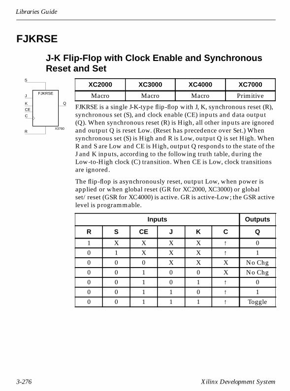
Libraries Guide
FJKRSE
J-K Flip-Flop with Clock Enable and SynchronousReset and Set
FJKRSE is a single J-K-type flip-flop with J, K, synchronous reset (R),synchronous set (S), and clock enable (CE) inputs and data output(Q). When synchronous reset (R) is High, all other inputs are ignoredand output Q is reset Low. (Reset has precedence over Set.) Whensynchronous set (S) is High and R is Low, output Q is set High. WhenR and S are Low and CE is High, output Q responds to the state of theJ and K inputs, according to the following truth table, during theLow-to-High clock (C) transition. When CE is Low, clock transitionsare ignored.
The flip-flop is asynchronously reset, output Low, when power isapplied or when global reset (GR for XC2000, XC3000) or globalset/reset (GSR for XC4000) is active. GR is active-Low; the GSR activelevel is programmable.
XC2000 XC3000 XC4000 XC7000
Macro Macro Macro Primitive
Inputs Outputs
R S CE J K C Q
1 X X X X ↑ 00 1 X X X ↑ 10 0 0 X X X No Chg0 0 1 0 0 X No Chg0 0 1 0 1 ↑ 00 0 1 1 0 ↑ 10 0 1 1 1 ↑ Toggle
Q
J
C
FJKRSE
K
S
CE
RX3760
3-276 Xilinx Development System
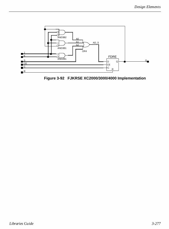
Design Elements
Figure 3-92 FJKRSE XC2000/3000/4000 Implementation
R
CCES
AD_S
JK
AND3B2
AND3B1
AND2B1Q
A0A1A2
OR4
FDRE
R
QDCEC
Libraries Guide 3-277

Libraries Guide
FJKSRE
J-K Flip-Flop with Clock Enable and SynchronousSet and Reset
FJKSRE is a single J-K-type flip-flop with J, K, synchronous set (S),synchronous reset (R), and clock enable (CE) inputs and data output(Q). When synchronous set (S) is High, all other inputs are ignoredand output Q is set High. (Set has precedence over Reset.) Whensynchronous reset (R) is High and S is Low, output Q is reset Low.When S and R are Low and CE is High, output Q responds to the stateof the J and K inputs, as shown in the following truth table, duringthe Low-to-High clock (C) transition. When CE is Low, clock transi-tions are ignored.
The flip-flop is asynchronously reset, output Low, when power isapplied or when global reset (GR for XC2000, XC3000) or globalset/reset (GSR for XC4000) is active. GR is active-Low; the GSR activelevel is programmable.
XC2000 XC3000 XC4000 XC7000
Macro Macro Macro Primitive
Inputs Outputs
S R CE J K C Q
1 X X X X ↑ 10 1 X X X ↑ 00 0 0 X X X No Chg0 0 1 0 0 X No Chg0 0 1 0 1 ↑ 00 0 1 1 0 ↑ 10 0 1 1 1 ↑ Toggle
Q
J
C
FJKSRE
K
S
CE
RX3759
3-278 Xilinx Development System
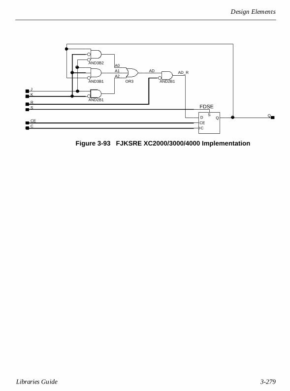
Design Elements
Figure 3-93 FJKSRE XC2000/3000/4000 Implementation
A2
A0A1
AND3B2
AND3B1 OR3
AD
AND2B1
AD_R
QCEC
SR
K
FDSE
SQD
CEC
J
AND2B1
Libraries Guide 3-279
Libraries Guide
FMAP
F Function Generator Partitioning Control Symbol
The FMAP symbol is used to control logic partitioning into XC4000family 4-input function generators. The place and route softwarechooses an F or a G function generator as a default, unless you specifyan F or G. Refer to the appropriate CAE tool interface user guide forinformation about specifying this attribute in your schematic designeditor.
The FMAP symbol is usually used with the HMAP symbol, whichpartitions logic into the 3-input generator of the Configurable LogicBlock (CLB). You can implement a portion of logic using gates,latches, and flip-flops, and specify the logic to be grouped into F, G,and H function generators by naming logic signals andFMAP/HMAP signals correspondingly. These symbols are used formapping control in addition to the actual gates, latches, and flip-flops, not as a substitute for them.
XC2000 XC3000 XC4000 XC7000
N/A N/A Primitive N/A
X4646
FMAP
I1
I2
I3
I4
O
3-280 Xilinx Development System

Design Elements
The following figure gives an example of how logic can be placedusing FMAP and HMAP symbols.
Figure 3-94 Partitioning Logic Using FMAP and HMAP Symbols
The MAP=type parameter can be used with the FMAP symbol tofurther define how much latitude you want to give the mappingprogram. The following table shows MAP option characters and theirmeanings.
Possible types of MAP parameters for FMAP are: MAP=PUC,MAP=PLC, MAP=PLO, and MAP=PUO. The default parameter is
Character Function
P PinsC Closed – Adding logic to or removing
logic from the CLB is not allowed.L Locked – Locking CLB pinsO Open – Adding logic to or removing logic
from the CLB is allowed.U Unlocked – No locking on CLB pins.
D0D1
SE
O
U3
M2-1
F_FUNC
U1
AND4
IN_F1
IN_F2
IN_F3
IN_F4
IN_G1D0
D1
SE
EN
O
U2
M2-1E
G_FUNCH_FUNC
IN_F1
IN_F2
IN_F3
IN_F4
I1
I2
I3
I4
O
U4
FMAPCLB_R*C*.F
F_FUNC
G_FUNC
I1
I2
I3
I4
O
U5
FMAPCLB_R*C*.G
IN_G1
IN_G2
IN_G3
IN_G2
IN_G3
IN_G4
IN_H1
IN_G4
F_FUNC
G_FUNCI1
I2
I3
O
U6
HMAP
H_FUNC
IN_H1
IN_H1
IN_F1
IN_F2
IN_F3
IN_F4F
HH_FUNC
G
IN_G1
IN_G2IN_G3
IN_G4
X1882
Libraries Guide 3-281

Libraries Guide
PUC. If one of the “open” parameters is used (PLO or PUO), only theoutput signals must be specified.
The FMAP symbol can be assigned to specific CLB locations usingLOC attributes. Refer to the appropriate CAE tool interface userguide for more information on assigning LOC attributes.
3-282 Xilinx Development System

Design Elements
FTC
Toggle Flip-Flop with Toggle Enable andAsynchronous Clear
FTC is a synchronous, resettable toggle flip-flop. The asynchronousclear (CLR) input, when High, overrides all other inputs and resetsthe data output (Q) Low. The Q output toggles, or changes state,when the toggle enable (T) input is High and CLR is Low during theLow-to-High clock transition.
The flip-flop is asynchronously reset, output Low, when power isapplied or when global reset (GR for XC2000, XC3000) or globalset/reset (GSR for XC4000) is active. GR is active-Low; the GSR activelevel is programmable.
Figure 3-95 FTC XC2000/3000/4000 Implementation
XC2000 XC3000 XC4000 XC7000
Macro Macro Macro Primitive
Inputs Outputs
CLR T C Q
1 X X 00 0 X No Chg0 1 ↑ Toggle
Q
X3761
T
CLR
C
FTC
XOR2
QTQ
CLR
C
T QD
CLRC
FDC
Libraries Guide 3-283
Libraries Guide
FTCE
Toggle Flip-Flop with Toggle and Clock Enable andAsynchronous Clear
When the asynchronous clear (CLR) input is High, all other inputsare ignored and the data output (Q) is reset Low. When CLR is Lowand toggle enable (T) and clock enable (CE) are High, Q outputtoggles, or changes state, during the Low-to-High clock (C) transi-tion. When CE is Low, clock transitions are ignored.
The flip-flop is asynchronously reset, output Low, when power isapplied or when global reset (GR for XC2000, XC3000) or globalset/reset (GSR for XC4000) is active. GR is active-Low; the GSR activelevel is programmable.
Figure 3-96 FTCE XC2000/3000/4000 Implementation
XC2000 XC3000 XC4000 XC7000
Macro Macro Macro Primitive
Inputs Outputs
CLR CE T C Q
1 X X X 00 0 X X No Chg0 1 0 X No Chg0 1 1 ↑ Toggle
QT FTCE
C
CLRX3764
CE
T
CEQ
XOR2
TQ FDCEQD
CLR
CECC
CLR
3-284 Xilinx Development System

Design Elements
FTCLE
Toggle/Loadable Flip-Flop with Toggle and ClockEnable and Asynchronous Clear
When the asynchronous clear input (CLR) is High, all other inputsare ignored and output Q is reset Low. When load enable input (L) isHigh and CLR is Low, clock enable (CE) is overridden and the dataon data input (D) is loaded into the flip-flop during the Low-to-Highclock (C) transition. When toggle enable (T) and CE are High and Land CLR are Low, output Q toggles, or changes state, during theLow- to-High clock transition. When CE is Low, clock transitions areignored.
The flip-flop is asynchronously reset, output Low, when power isapplied or when global reset (GR for XC2000, XC3000) or globalset/reset (GSR for XC4000) is active. GR is active-Low; the GSR activelevel is programmable.
XC2000 XC3000 XC4000 XC7000
Macro Macro Macro Primitive
Inputs Outputs
CLR L CE T D C Q
1 X X X X X 00 1 X X 1 ↑ 10 1 X X 0 ↑ 00 0 0 X X X No Chg0 0 1 0 X X No Chg0 0 1 1 X ↑ Toggle
X3769
FTCLE
C
CE
T
L
D
CLR
Q
Libraries Guide 3-285

Libraries Guide
Figure 3-97 FTCLE XC2000/3000/4000 Implementation
FDCE
QD
CLR
CEC
D0D1
O
S0
M2_1XOR2
T
CLR
MD
Q
TQ
D
C
L_CE
L
CE
OR2
3-286 Xilinx Development System

Design Elements
FTCP
Toggle Flip-Flop with Toggle Enable andAsynchronous Clear and Preset
* not supported for XC7336 designs
When the asynchronous clear (CLR) input is High, all other inputsare ignored and the output (Q) is reset Low. When the asynchronouspreset (PRE) input is High (provided CLR is Low), all other inputsare ignored and Q is set High. When the toggle enable input (T) isHigh and CLR and PRE are Low, output Q toggles, or changes state,during the Low-to-High clock (C) transition.
The flip-flop is asynchronously reset, output Low, when power isapplied or when global reset (GR) is active (Low).
Figure 3-98 FTCP XC2000 Implementation
XC2000 XC3000 XC4000 XC7000
Macro N/A N/A Primitive*
Inputs Outputs
CLR PRE T C Q
1 X X X 00 1 X X 10 0 0 X No Chg0 0 1 ↑ Toggle
Q
T
C
FTCP
PRE
CLR X4392
XOR2
QTQ
C
T
CLR
PRE
C CLR
D PRE Q
FDCP
Libraries Guide 3-287
Libraries Guide
FTCPE
Toggle Flip-Flop with Toggle and Clock Enable andAsynchronous Clear and Preset
* not supported for XC7336 designs
When the asynchronous clear (CLR) input is High, all other inputsare ignored and the output (Q) is reset Low. When the asynchronouspreset (PRE) input is High (provided CLR is Low), all other inputs areignored and Q is set High. When the toggle enable input (T) and theclock enable input (CE) are High and CLR and PRE are Low, outputQ toggles, or changes state, during the Low-to-High clock (C) transi-tion. Clock transitions are ignored when CE is Low.
The flip-flop is asynchronously reset, output Low, when power isapplied or when global reset (GR) is active (Low).
Figure 3-99 FTCPE XC2000 Implementation
XC2000 XC3000 XC4000 XC7000
Macro N/A N/A Primitive*
Inputs Outputs
CLR PRE CE T C Q
1 X X X X 00 1 X X X 10 0 0 X X No Chg0 0 1 0 X No Chg0 0 1 1 ↑ Toggle
Q
T
C
FTCPE
CE
PRE
CLR X4393
CE
CLR
C
XOR2
QTQT
PRE
C
CED Q
CLR
PRE
PFE
3-288 Xilinx Development System
Design Elements
FTCPLE
Loadable Toggle Flip-Flop with Toggle and ClockEnable and Asynchronous Clear and Preset
* not supported for XC7336 designs
When the asynchronous clear (CLR) input is High, all other inputsare ignored and the output (Q) is reset Low. When the asynchronouspreset (PRE) input is High (provided CLR is Low), all other inputsare ignored and Q is set High. The load input (L) loads the data oninput D into the flip-flop on the Low-to-High clock transition, regard-less of the state of the clock enable (CE). When the toggle enableinput (T) and the clock enable input (CE) are High and CLR, PRE,and L are Low, output Q toggles, or changes state, during the Low-to-High clock (C) transition. Clock transitions are ignored when CE isLow.
The flip-flop is asynchronously reset, output Low, when power isapplied or when global reset (GR) is active (Low).
XC2000 XC3000 XC4000 XC7000
Macro N/A N/A Primitive*
Inputs Outputs
CLR PRE L CE T C D Q
1 X X X X X X 00 1 X X X X X 10 0 1 X X ↑ 0 00 0 1 X X ↑ 1 10 0 0 0 X X X No Chg0 0 0 1 0 X X No Chg0 0 0 1 1 ↑ X Toggle
Q
D
C
FTCPLE
CE
PRE
CLR X4394
T
L
Libraries Guide 3-289

Libraries Guide
Figure 3-100 FTCPLE XC2000 Implementation
PRE
CCED Q
CLR
PRE
FDCPE
C
CLR
CEL_CE
D0D1
O
S0
M2_1XOR2
T
MD
TQ
DL
Q
OR2
3-290 Xilinx Development System

Design Elements
FTP
Toggle Flip-Flop with Toggle Enable andAsynchronous Preset
When the asynchronous preset (PRE) input is High, all other inputsare ignored and output Q is set High. When toggle enable input (T) isHigh and PRE is Low, output Q toggles, or changes state, during theLow-to-High clock (C) transition. The flip-flop is asynchronously set,output High, when global set/reset (GSR) is active. The GSR activelevel is programmable.
Figure 3-101 FTP XC4000 Implementation
XC2000 XC3000 XC4000 XC7000
N/A N/A Macro Primitive
Inputs Outputs
PRE T C Q
1 X X 10 0 X No Chg0 1 ↑ Toggle
Q
X3762
TFTP
C
PRE
QTQ
PRE
XOR2C
T QPRED
C
FDP
Libraries Guide 3-291

Libraries Guide
FTPE
Toggle Flip-Flop with Toggle and Clock Enable andAsynchronous Preset
When the asynchronous preset (PRE) input is High, all other inputsare ignored and output Q is set High during the Low-to-High clock(C) transition. When the toggle enable input (T) is High, clock enable(CE) is High, and PRE is Low, output Q toggles, or changes state,during the Low-to-High clock transition. When CE is Low, clock tran-sitions are ignored. The flip-flop is asynchronously set, output High,when global set/reset (GSR) is active. The GSR active level isprogrammable.
Figure 3-102 FTPE XC4000 Implementation
XC2000 XC3000 XC4000 XC7000
N/A N/A Macro Primitive
Inputs Outputs
PRE CE T C Q
1 X X X 10 0 X X No Chg0 1 0 X No Chg0 1 1 ↑ Toggle
X3765
FTPE
C
CE
QT
PRE
CCED
PREQ
FDPE
QT
XOR2
TQ
CEC
PRE
3-292 Xilinx Development System

Design Elements
FTPLE
Toggle/Loadable Flip-Flop with Toggle and ClockEnable and Asynchronous Preset
When the asynchronous preset input (PRE) is High, all other inputsare ignored and output Q is set High during the Low-to-High clock(C) transition. When the load enable input (L) is High and PRE isLow, the clock enable (CE) is overridden and the data on input (D) isloaded into the flip-flop during the Low-to-High clock transition.When L and PRE are Low and toggle enable input (T) and CE areHigh, output Q toggles, or changes state, during the Low-to-Highclock transition. When CE is Low, clock transitions are ignored. Theflip-flop is asynchronously set, output High, when global set/reset(GSR) is active. The GSR active level is programmable.
XC2000 XC3000 XC4000 XC7000
N/A N/A Macro Primitive
Inputs Outputs
PRE L CE T D C Q
1 X X X X X 10 1 X X 1 ↑ 10 1 X X 0 ↑ 00 0 0 X X X No Chg0 0 1 0 X X No Chg0 0 1 1 X ↑ Toggle
X3770
C
CE
T
L
D
Q
PRE
FTPLE
Libraries Guide 3-293

Libraries Guide
Figure 3-103 FTPLE XC4000 Implementation
C
PRE
CE
OR2CCED PRE Q
FDPE
D
TQ
Q
T
XOR2 D0D1
O
S0
M2_1
L
MD
3-294 Xilinx Development System

Design Elements
FTRSE
Toggle Flip-Flop with Toggle and Clock Enable andSynchronous Reset and Set
When the synchronous reset input (R) is High, it overrides all otherinputs and the data output (Q) is reset Low. When the synchronousset input (S) is High and R is Low, clock enable input (CE) is over-ridden and output Q is set High. (Reset has precedence over Set.)When toggle enable input (T) and CE are High and R and S are Low,output Q toggles, or changes state, during the Low-to-High clocktransition.
The flip-flop is asynchronously reset, output Low, when power isapplied or when global reset (GR for XC2000, XC3000) or globalset/reset (GSR for XC4000) is active. GR is active-Low; the GSR activelevel is programmable.
Figure 3-104 FTRSE XC2000/3000/4000 Implementation
XC2000 XC3000 XC4000 XC7000
Macro Macro Macro Primitive
Inputs Outputs
R S CE T C Q
1 X X X ↑ 00 1 X X ↑ 10 0 0 X X No Chg0 0 1 0 X No Chg0 0 1 1 ↑ Toggle
X3768
FTRSE
C
CE
QT
R
S
S
T
RCCE
OR2
QCE_S
XOR2 D_S
TQ
FDRE
R
QDCEC
OR2
Libraries Guide 3-295

Libraries Guide
FTRSLE
Toggle/Loadable Flip-Flop with Toggle and ClockEnable and Synchronous Reset and Set
The synchronous reset input (R), when High, overrides all otherinputs and resets the data output (Q) Low. (Reset has precedence overSet.) When R is Low and synchronous set input (S) is High, the clockenable input (CE) is overridden and output Q is set High. When Rand S are Low and load enable input (L) is High, CE is overriddenand data on data input (D) is loaded into the flip-flop during theLow-to-High clock transition. When R, S, and L are Low and CE isHigh, output Q toggles, or changes state, during the Low-to-Highclock transition. When CE is Low, clock transitions are ignored.
The flip-flop is asynchronously reset, output Low, when power isapplied or when global reset (GR for XC2000, XC3000) or globalset/reset (GSR for XC4000) is active. GR is active-Low; the GSR activelevel is programmable.
XC2000 XC3000 XC4000 XC7000
Macro Macro Macro Primitive
Inputs Outputs
R S L CE T D C Q
1 0 X X X X ↑ 00 1 X X X X ↑ 10 0 1 X X 1 ↑ 10 0 1 X X 0 ↑ 00 0 0 0 X X X No Chg0 0 0 1 0 X X No Chg0 0 0 1 1 X ↑ Toggle
X3773
FTRSLE
C
CE
T
L
D
R
Q
S
3-296 Xilinx Development System

Design Elements
Figure 3-105 FTRSLE XC2000/3000/4000 Implementation
SL
R
C
CE_S_L
MD_S
Q
TQT
D
XOR2D0D1
O
S0
M2_1MD
FDRE
R
QDCEC
CEOR3
OR2
Libraries Guide 3-297

Libraries Guide
FTSRE
Toggle Flip-Flop with Toggle and Clock Enable andSynchronous Set and Reset
The synchronous set input, when High, overrides all other inputs andsets data output (Q) High. (Set has precedence over Reset.) Whensynchronous reset input (R) is High and S is Low, clock enable input(CE) is overridden and output Q is reset Low. When toggle enableinput (T) and CE are High and S and R are Low, output Q toggles, orchanges state, during the Low-to-High clock transition.
The flip-flop is asynchronously reset, output Low, when power isapplied or when global reset (GR for XC2000, XC3000) or globalset/reset (GSR for XC4000) is active. GR is active-Low; the GSR activelevel is programmable.
Figure 3-106 FTSRE XC2000/3000/4000 Implementation
XC2000 XC3000 XC4000 XC7000
Macro Macro Macro Primitive
Inputs Outputs
S R CE T C Q
1 X X X ↑ 10 1 X X ↑ 00 0 0 X X No Chg0 0 1 0 X No Chg0 0 1 1 ↑ Toggle
X3767
FTSRE
C
CE
QT
R
S
COR2
Q
FDSE
SQD
CE
C
CE_R
XOR2
T
AND2B1
R
CE
S
D_R
TQ
3-298 Xilinx Development System

Design Elements
FTSRLE
Toggle/Loadable Flip-Flop with Toggle and ClockEnable and Synchronous Set and Reset
The synchronous set input (S), when High, overrides all other inputsand sets data output (Q) High. (Set has precedence over Reset.) Whensynchronous reset (R) is High and S is Low, clock enable input (CE) isoverridden and output Q is reset Low. When load enable input (L) isHigh and S and R are Low, CE is overridden and data on data input(D) is loaded into the flip-flop during the Low-to-High clock transi-tion. When the toggle enable input (T) and CE are High and S, R, andL are Low, output Q toggles, or changes state, during the Low-to-High clock transition. When CE is Low, clock transitions are ignored.
The flip-flop is asynchronously reset, output Low, when power isapplied or when global reset (GR for XC2000, XC3000) or globalset/reset (GSR for XC4000) is active. GR is active-Low; the GSR activelevel is programmable.
XC2000 XC3000 XC4000 XC7000
Macro Macro Macro Primitive
Inputs Outputs
S R L CE T D C Q
1 0 X X X X ↑ 10 1 X X X X ↑ 00 0 1 X X 1 ↑ 10 0 1 X X 0 ↑ 00 0 0 0 X X X No Chg0 0 0 1 0 X X No Chg0 0 0 1 1 X ↑ Toggle
X3772
FTSRLE
C
CE
T
L
D
R
Q
S
Libraries Guide 3-299

Libraries Guide
Figure 3-107 FTSRLE XC2000/3000/4000 Implementation
AND2B1
MDD0D1
O
S0
M2_1XOR2
D
TTQ
CE
Q
S
LR
OR3
FDSES
QDCEC
C
CE_R_L
MD_S
3-300 Xilinx Development System
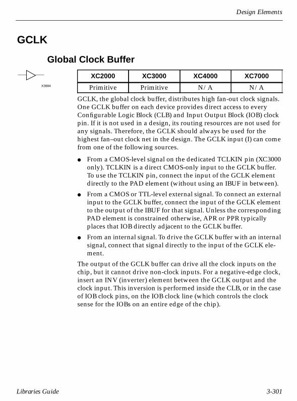
Design Elements
GCLK
Global Clock Buffer
GCLK, the global clock buffer, distributes high fan-out clock signals.One GCLK buffer on each device provides direct access to everyConfigurable Logic Block (CLB) and Input Output Block (IOB) clockpin. If it is not used in a design, its routing resources are not used forany signals. Therefore, the GCLK should always be used for thehighest fan–out clock net in the design. The GCLK input (I) can comefrom one of the following sources.
● From a CMOS-level signal on the dedicated TCLKIN pin (XC3000only). TCLKIN is a direct CMOS-only input to the GCLK buffer.To use the TCLKIN pin, connect the input of the GCLK elementdirectly to the PAD element (without using an IBUF in between).
● From a CMOS or TTL-level external signal. To connect an externalinput to the GCLK buffer, connect the input of the GCLK elementto the output of the IBUF for that signal. Unless the correspondingPAD element is constrained otherwise, APR or PPR typicallyplaces that IOB directly adjacent to the GCLK buffer.
● From an internal signal. To drive the GCLK buffer with an internalsignal, connect that signal directly to the input of the GCLK ele-ment.
The output of the GCLK buffer can drive all the clock inputs on thechip, but it cannot drive non-clock inputs. For a negative-edge clock,insert an INV (inverter) element between the GCLK output and theclock input. This inversion is performed inside the CLB, or in the caseof IOB clock pins, on the IOB clock line (which controls the clocksense for the IOBs on an entire edge of the chip).
XC2000 XC3000 XC4000 XC7000
Primitive Primitive N/A N/AX3884
Libraries Guide 3-301

Libraries Guide
GND
Ground-Connection Signal Tag
The GND signal tag, or parameter, forces a net or input function to aLow logic level. A net tied to GND cannot have any other source.
When the logic-trimming software (XNFPrep) or fitter (XEPLD)encounters a net or input function tied to GND, it removes any logicthat is disabled by the GND signal. The GND signal is only imple-mented when the disabled logic cannot be removed.
XC2000 XC3000 XC4000 XC7000
Primitive Primitive Primitive PrimitiveX3858
3-302 Xilinx Development System

Design Elements
GXTL
Crystal Oscillator with ACLK Buffer
The GXTL element drives an internal ACLK buffer with a frequencyderived from an external crystal-controlled oscillator. The GXTL (orACLK) output is connected to an internal clock net.
There are two dedicated input pins (XTAL 1 and XTAL 2) on eachFPGA device that are internally connected to pads and input/outputblocks that are in turn connected to the GXTL amplifier. The externalcomponents are connected as shown in the following example. Referto The Programmable Gate Array Data Book for details on componentselection and tolerances.
Figure 3-108 GXTL XC2000/3000 Implementation
XC2000 XC3000 XC4000 XC7000
Macro Macro N/A N/A
X3886
ACLK
@PULSELO=@PULSEL
@PULSEHI=@PULSEH
OSC
OSC_OUT O
Libraries Guide 3-303

Libraries Guide
HMAP
H Function Generator Partitioning Control Symbol
The HMAP symbol is used to control logic partitioning into XC4000family 3-input H function generators. It is usually used with FMAP,which partitions logic into F and G function generators. You canimplement a portion of logic using gates, latches, and flip-flops andspecify the logic to be grouped into F, G, and H function generatorsby naming logic signals and HMAP/FMAP signals correspondingly.These symbols are used for mapping control in addition to the actualgates, latches, and flip-flops and not as a substitute for them. Thefollowing figure gives an example of how logic can be placed usingHMAP and FMAP symbols.
Figure 3-109 Partitioning Logic Using FMAP and HMAPSymbols
XC2000 XC3000 XC4000 XC7000
N/A N/A Primitive N/A
X4659
HMAP
I1
I2
I3
O
D0D1
SE
O
U3
M2-1
F_FUNC
U1
AND4
IN_F1
IN_F2
IN_F3
IN_F4
IN_G1D0
D1
SE
EN
O
U2
M2-1E
G_FUNCH_FUNC
IN_F1
IN_F2
IN_F3
IN_F4
I1
I2
I3
I4
O
U4
FMAPCLB_R*C*.F
F_FUNC
G_FUNC
I1
I2
I3
I4
O
U5
FMAPCLB_R*C*.G
IN_G1
IN_G2
IN_G3
IN_G2
IN_G3
IN_G4
IN_H1
IN_G4
F_FUNC
G_FUNCI1
I2
I3
O
U6
HMAP
H_FUNC
IN_H1
IN_H1
IN_F1
IN_F2
IN_F3
IN_F4
F
HH_FUNC
G
IN_G1
IN_G2IN_G3
IN_G4
X1882
3-304 Xilinx Development System
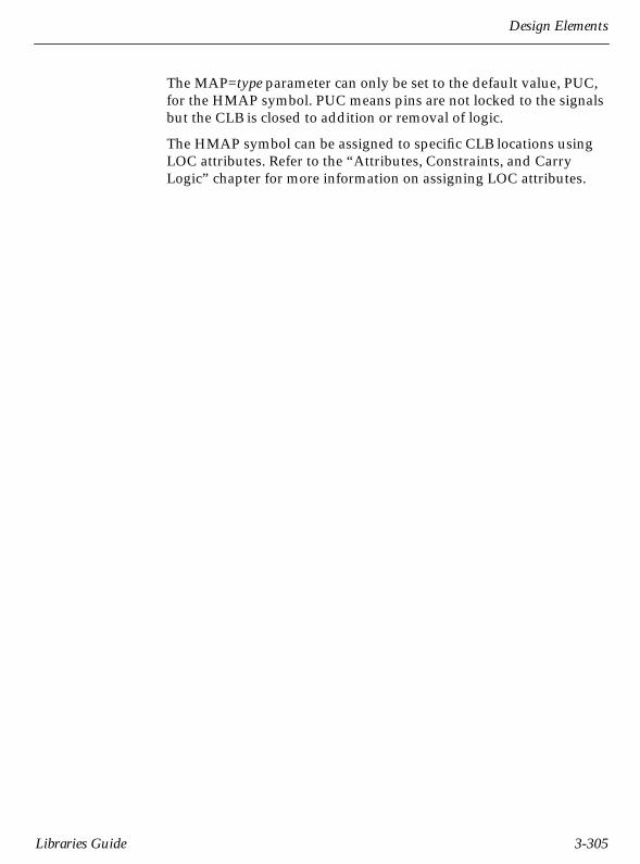
Design Elements
The MAP=type parameter can only be set to the default value, PUC,for the HMAP symbol. PUC means pins are not locked to the signalsbut the CLB is closed to addition or removal of logic.
The HMAP symbol can be assigned to specific CLB locations usingLOC attributes. Refer to the “Attributes, Constraints, and CarryLogic” chapter for more information on assigning LOC attributes.
Libraries Guide 3-305

Libraries Guide
IBUF, IBUF4, IBUF8, and IBUF16
Single- and Multiple-Input Buffers
IBUF, IBUF4, IBUF8, and IBUF16 are single and multiple inputbuffers. An IBUF isolates the internal circuit from the signals cominginto a chip. IBUFs are contained in input/output blocks (IOB). IBUFinputs (I) are connected to an IPAD or an IOPAD. IBUF outputs (O)are connected to the internal circuit.
Figure 3-110 IBUF8 XC2000/3000/4000/7000 Implementation
Name XC2000 XC3000 XC4000 XC7000
IBUF Primitive Primitive Primitive PrimitiveIBUF4,IBUF8,IBUF16
Macro Macro Macro Macro
X3784
X3791
IBUF4
IBUF8
X3803
IBUF16
X3815
IBUF
IBUF
IBUF
IBUF
IBUF
IBUF
IBUF
IBUF
O7
O6
O[7:0]
O0
O1
O2
O3
O4
O5
I[7:0]
I0
I1
I2
I3
I4
I5
I6
I7
3-306 Xilinx Development System
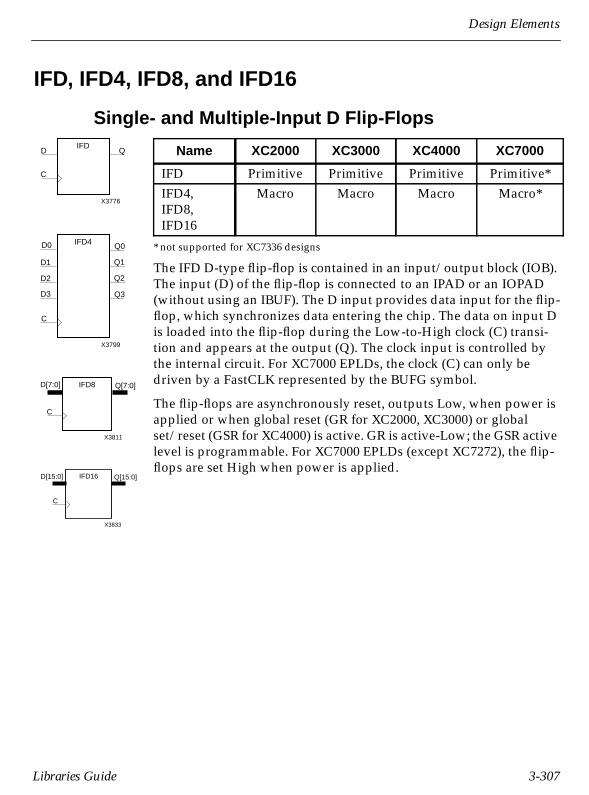
Design Elements
IFD, IFD4, IFD8, and IFD16
Single- and Multiple-Input D Flip-Flops
* not supported for XC7336 designs
The IFD D-type flip-flop is contained in an input/output block (IOB).The input (D) of the flip-flop is connected to an IPAD or an IOPAD(without using an IBUF). The D input provides data input for the flip-flop, which synchronizes data entering the chip. The data on input Dis loaded into the flip-flop during the Low-to-High clock (C) transi-tion and appears at the output (Q). The clock input is controlled bythe internal circuit. For XC7000 EPLDs, the clock (C) can only bedriven by a FastCLK represented by the BUFG symbol.
The flip-flops are asynchronously reset, outputs Low, when power isapplied or when global reset (GR for XC2000, XC3000) or globalset/reset (GSR for XC4000) is active. GR is active-Low; the GSR activelevel is programmable. For XC7000 EPLDs (except XC7272), the flip-flops are set High when power is applied.
Name XC2000 XC3000 XC4000 XC7000
IFD Primitive Primitive Primitive Primitive*IFD4,IFD8,IFD16
Macro Macro Macro Macro*
Q
X3776
DIFD
C
Q[7:0]
X3811
D[7:0] IFD8
C
Q[15:0]
X3833
D[15:0] IFD16
C
X3799
IFD4
C
D3
D2
D1
D0
Q3
Q2
Q1
Q0
Libraries Guide 3-307

Libraries Guide
Refer to the following figures for legal IFD/ILD combinations forXC3000 and XC4000 respectively.
Figure 3-111 Legal Combinations of IFD and ILD for a SingleDevice Edge of XC3000 IOB
Figure 3-112 Legal Combinations of IFD and ILD for a SingleXC4000 IOB
dn = state of referenced input one set-up time prior to active clock transition
Inputs Outputs
Dn C Qn
Dn ↑ dn
X4690
D Q
D Q
G
C C
ILD
IFD_1
IPAD
IPADD Q
D Q
G
ILD_1
IFD
IPAD
IPAD
X4688
D Q
D Q
G
C C
ILD
IFD_1
IPAD
D Q
D Q
G
ILD_1
IFD
IPAD
CLOCKCLOCK
3-308 Xilinx Development System

Design Elements
Figure 3-113 IFD8 XC2000/3000/4000/7000 Implementation
D[7:0]
D7
D6
D5
D0
D1
D2
D3
D4
C
Q[7:0]
Q0
Q2
Q3
Q4
Q5
Q7
Q6
Q1
Q7
IFD
QD
C
Q6
IFD
QD
C
Q5
IFD
QD
C
Q4
IFDQD
C
Q3
IFD
QD
C
Q2
IFDQD
C
Q1
IFDQD
C
Q0
IFD
QD
C
Libraries Guide 3-309

Libraries Guide
IFD_1
Input D Flip-Flop with Inverted Clock
The IFD_1 D-type flip-flop is contained in an input/output block(IOB). The input (D) of the flip-flop is connected to an IPAD or anIOPAD. The D input also provides data input for the flip-flop, whichsynchronizes data entering the chip. The data on input D is loadedinto the flip-flop during the High-to-Low clock (C) transition andappears at the output (Q). The clock input is controlled by the internalcircuit.
The flip-flop is asynchronously reset, output Low, when power isapplied or when global reset (GR for XC2000, XC3000) or globalset/reset (GSR for XC4000) is active. GR is active-Low; the GSR activelevel is programmable.
Refer to the following figures for legal IFD/ILD combinations forXC3000 and XC4000 respectively.
Figure 3-114 Legal Combinations of IFD and ILD for a SingleDevice Edge of XC3000 IOB
XC2000 XC3000 XC4000 XC7000
Macro Macro Macro N/A
Q
X3777
DIFD_1
C
X4690
D Q
D Q
G
C C
ILD
IFD_1
IPAD
IPADD Q
D Q
G
ILD_1
IFD
IPAD
IPAD
3-310 Xilinx Development System

Design Elements
Figure 3-115 Legal Combinations of IFD and ILD for a SingleXC4000 IOB
d = state of referenced input one set-up time prior to active clock transition
Figure 3-116 IFD_1 XC2000/3000/4000 Implementation
Inputs Outputs
D C Q
D ↓ d
X4688
D Q
D Q
G
C C
ILD
IFD_1
IPAD
D Q
D Q
G
ILD_1
IFD
IPAD
CLOCKCLOCK
CB
Q
C
D
INV
IFDQD
C
Libraries Guide 3-311

Libraries Guide
IFDX1, IFD4X1, IFD8X1, and IFD16X1
Input D Flip-Flops for EPLD
* not supported for XC7236, XC7272, or XC7336 designs
The IFDX1 symbols are D-type flip-flops with synchronous clockenable implemented in the input blocks of an EPLD device. They arecommonly used to synchronize and store data entering a chip. Thedata input (D) of the flip-flop is connected directly to an IPAD or anIOPAD (without using an IBUF). When the clock enable (CE) input isLow, the data on input D is loaded into the flip-flop during the Low-to-High clock (C) transition and appears at the output (Q). The flip-flop ignores clock transitions when CE is High.
The clock input (C) must be driven by a global FastCLK net of theEPLD device, represented by the BUFG symbol. The clock enableinput (CE) must be driven by a global clock enable net of the EPLDdevice, represented by the BUFCE symbol.
The flip-flops are asynchronously set, outputs High, when power isapplied or when the device Master Reset pin is activated.
Name XC2000 XC3000 XC4000 XC7000
IFDX1 N/A N/A N/A Primitive*IFD4X1,IFD8X1,IFD16X1
N/A N/A N/A Macro*
Inputs Outputs
D CE C Q
X 1 X No Chg0 0 ↑ 01 0 ↑ 1
X4213
IFDX1
CCE
D Q
X4216
IFD4X1
C
D3
D2
D1
D0 Q0
Q1
Q2
Q3CE
X4219
IFD8X1
CCE
D[7:0] Q[7:0]
X4222
IFD16X1
CCE
D[15:0] Q[15:0]
3-312 Xilinx Development System

Design Elements
Figure 3-117 IFD8X1 XC7000 Implementation
Q6
C
IFDX1
QDCE
Q1
Q6
Q7
Q5
Q4
Q3
Q2
Q0
Q[7:0]
C
D4
D3
D2
D1
D0
D5
D6
D7
D[7:0]
CE
Q0
C
IFDX1
QDCE
Q1
C
IFDX1
QDCE
Q2
C
IFDX1
QDCE
Q3
C
IFDX1
QDCE
Q4
C
IFDX1
QDCE
Q5
C
IFDX1
QDCE
Q7
C
IFDX1
QDCE
Libraries Guide 3-313
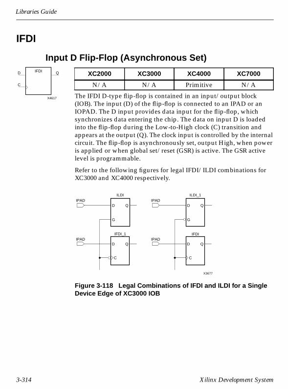
Libraries Guide
IFDI
Input D Flip-Flop (Asynchronous Set)
The IFDI D-type flip-flop is contained in an input/output block(IOB). The input (D) of the flip-flop is connected to an IPAD or anIOPAD. The D input provides data input for the flip-flop, whichsynchronizes data entering the chip. The data on input D is loadedinto the flip-flop during the Low-to-High clock (C) transition andappears at the output (Q). The clock input is controlled by the internalcircuit. The flip-flop is asynchronously set, output High, when poweris applied or when global set/reset (GSR) is active. The GSR activelevel is programmable.
Refer to the following figures for legal IFDI/ILDI combinations forXC3000 and XC4000 respectively.
Figure 3-118 Legal Combinations of IFDI and ILDI for a SingleDevice Edge of XC3000 IOB
XC2000 XC3000 XC4000 XC7000
N/A N/A Primitive N/A
Q
X4617
D IFDI
C
X3677
D Q
D Q
G
C C
ILDI
IFDI_1
IPAD
IPADD Q
D Q
G
ILDI_1
IFDI
IPAD
IPAD
3-314 Xilinx Development System

Design Elements
Figure 3-119 Legal Combinations of IFDI and ILDI for a SingleXC4000 IOB
d = state of referenced input one set-up time prior to active clock transition
Inputs Outputs
D C Q
D ↑ d
X4511
D Q
D Q
G
C C
ILDI
IFDI_1
IPAD
D Q
D Q
G
ILDI_1
IFDI
IPAD
CLOCKCLOCK
Libraries Guide 3-315

Libraries Guide
IFDI_1
D Flip-Flop with Inverted Clock (Asynchronous Set)
The IFDI_1 D-type flip-flop is contained in an input/output block(IOB). The input (D) of the flip-flop is connected to an IPAD or anIOPAD. The D input provides data input for the flip-flop, whichsynchronizes data entering the chip. The data on input D is loadedinto the flip-flop during the High-to-Low clock (C) transition andappears at the output (Q). The clock input is controlled by the internalcircuit. The flip-flop is asynchronously set, output High, when poweris applied or when global set/reset (GSR) is active. The GSR activelevel is programmable.
Refer to the following figures for legal IFDI/ILDI combinations forXC3000 and XC4000 respectively.
Figure 3-120 Legal Combinations of IFDI and ILDI for a SingleXC4000 IOB
d = state of referenced input one set-up time prior to active clock transition
XC2000 XC3000 XC4000 XC7000
N/A N/A Macro N/A
Inputs Outputs
D C Q
D ↓ d
Q
X4386
D IFDI_1
C
X4511
D Q
D Q
G
C C
ILDI
IFDI_1
IPAD
D Q
D Q
G
ILDI_1
IFDI
IPAD
CLOCKCLOCK
3-316 Xilinx Development System
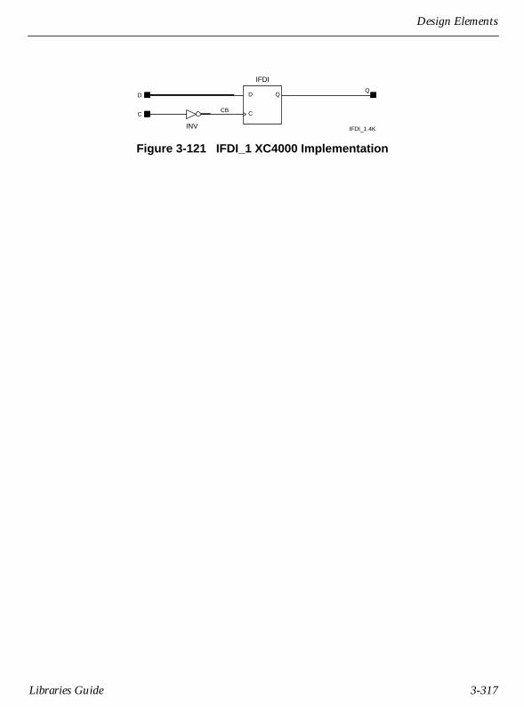
Design Elements
Figure 3-121 IFDI_1 XC4000 Implementation
CB
Q
C
D
INV
C
D Q
IFDI
IFDI_1.4K
Libraries Guide 3-317

Libraries Guide
ILD, ILD4, ILD8, and ILD16
Input Transparent Data Latches
* not supported for XC7336 designs
ILD, ILD4, ILD8, and ILD16 are single or multiple transparent datalatches, which can be used to hold transient data entering a chip. Thelatch input (D) is connected to an IPAD or an IOPAD (without usingan IBUF). When the gate input (G) is High, data on the inputs (D)appears on the outputs (Q). Data on the D inputs during the High-to-Low G transition is stored in the latch. For XC7000 EPLDs, the gateinput (G) must be driven by a FastCLK, represented by the BUFGsymbol.
The latch is reset, output Low, when power is applied or when globalreset (GR for XC3000) or global set/reset (GSR for XC4000) is active.GR is active-Low; the GSR active level is programmable. For XC7000EPLDs (except XC7272) the latches are set High when power isapplied.
XC4000 ILDThe XC4000 ILD is actually the input flip-flop master latch. It ispossible to access two different outputs from the input flip-flop: onethat responds to the level of the clock signal and another thatresponds to an edge of the clock signal. When using both outputsfrom the same input flip-flop, a transparent High latch (ILD) corre-sponds to a falling edge-triggered flip-flop (IFD_1). Similarly, a trans-parent Low latch (ILD_1) corresponds to a rising edge-triggered flip-flop (IFD). Refer to the following figure for XC4000 legal IFD/ILDcombinations.
Name XC2000 XC3000 XC4000 XC7000
ILD N/A Primitive Macro Primitive*ILD4,ILD8,ILD16
N/A Macro Macro Macro*
Q
X3774
D ILD
G
X3798
ILD4
G
D3
D2
D1
D0
Q3
Q2
Q1
Q0
Q[7:0]
X3810
D[7:0] ILD8
G
Q[15:0]
X3832
D[15:0] ILD16
G
3-318 Xilinx Development System
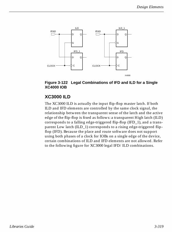
Design Elements
Figure 3-122 Legal Combinations of IFD and ILD for a SingleXC4000 IOB
XC3000 ILDThe XC3000 ILD is actually the input flip-flop master latch. If bothILD and IFD elements are controlled by the same clock signal, therelationship between the transparent sense of the latch and the activeedge of the flip-flop is fixed as follows: a transparent High latch (ILD)corresponds to a falling edge-triggered flip-flop (IFD_1), and a trans-parent Low latch (ILD_1) corresponds to a rising edge-triggered flip-flop (IFD). Because the place and route software does not supportusing both phases of a clock for IOBs on a single edge of the device,certain combinations of ILD and IFD elements are not allowed. Referto the following figure for XC3000 legal IFD/ILD combinations.
X4688
D Q
D Q
G
C C
ILD
IFD_1
IPAD
D Q
D Q
G
ILD_1
IFD
IPAD
CLOCKCLOCK
Libraries Guide 3-319

Libraries Guide
Figure 3-123 Legal Combinations of IFD and ILD for a SingleDevice Edge of XC3000 IOB
d = state of referenced input one set-up time prior to High-to-Low gate transition
Figure 3-124 ILD XC4000 Implementation
Inputs Outputs
G D Q
1 1 11 0 0↓ D d
X4690
D Q
D Q
G
C C
ILD
IFD_1
IPAD
IPADD Q
D Q
G
ILD_1
IFD
IPAD
IPAD
GB
Q
G
D
INV
ILD_1
D Q
G
ILD.4K
3-320 Xilinx Development System

Design Elements
Figure 3-125 ILD8 XC3000/4000/7000 Implementation
Q7G
D Q
ILD
Q5G
D Q
ILD
Q6G
D Q
ILD
Q4G
D Q
ILDQ3
G
D Q
ILDQ2
G
D Q
ILDQ1
G
D Q
ILDQ0
G
D Q
ILD
G
Q[7:0]
Q1
Q6
Q7
Q5
Q4
Q3
Q2
Q0
D7
D6
D5
D0
D1
D2
D3
D4
D[7:0]
Libraries Guide 3-321

Libraries Guide
ILD_1
Transparent Input Data Latch with Inverted Gate
ILD_1 is a transparent data latch, which can be used to hold transientdata entering a chip. When the gate input (G) is Low, data on the datainput (D) appears on the data output (Q). Data on D during the Low-to-High G transition is stored in the latch. For implementation details,refer to the “ILD, ILD4, ILD8, and ILD16” section earlier in thischapter.
The latch is reset, output Low, when power is applied or when globalreset (GR for XC3000) or global set/reset (GSR for XC4000) is active.GR is active-Low; the GSR active level is programmable.
Refer to the following figures for legal IFD/ILD combinations, forXC3000 and XC4000 respectively.
Figure 3-126 Legal Combinations of IFD and ILD for a SingleDevice Edge of XC3000 IOB
XC2000 XC3000 XC4000 XC7000
N/A Macro Primitive N/A
Q
X4387
D ILD_1
G
X4690
D Q
D Q
G
C C
ILD
IFD_1
IPAD
IPADD Q
D Q
G
ILD_1
IFD
IPAD
IPAD
3-322 Xilinx Development System
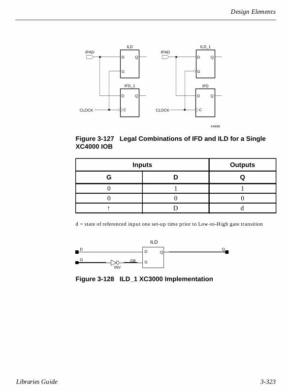
Design Elements
Figure 3-127 Legal Combinations of IFD and ILD for a SingleXC4000 IOB
d = state of referenced input one set-up time prior to Low-to-High gate transition
Figure 3-128 ILD_1 XC3000 Implementation
Inputs Outputs
G D Q
0 1 10 0 0↑ D d
X4688
D Q
D Q
G
C C
ILD
IFD_1
IPAD
D Q
D Q
G
ILD_1
IFD
IPAD
CLOCKCLOCK
D
G
Q
ILD
INV
D
G
Q
GB
Libraries Guide 3-323

Libraries Guide
ILDI
Input Transparent Data Latch (Asynchronous Set)
ILDI is a transparent data latch, which can hold transient dataentering a chip. When the gate input (G) is High, data on the input(D) appears on the output (Q). Data on the D input during the High-to-Low G transition is stored in the latch.
The ILDI is actually the input flip-flop master latch. It is possible toaccess two different outputs from the input flip-flop: one thatresponds to the level of the clock signal and another that responds toan edge of the clock signal. When using both outputs from the sameinput flip-flop, a transparent High latch (ILDI) corresponds to afalling edge-triggered flip-flop (IFDI_1). Similarly, a transparent Lowlatch (ILDI_1) corresponds to a rising edge-triggered flip-flop (IFDI).Refer to the following figures for legal IFDI/ILDI combinations forXC3000 and XC4000 respectively.
Figure 3-129 Legal Combinations of IFDI and ILDI for a SingleXC4000 IOB
The latch is set, output High, when power is applied or when globalset/reset (GSR) is active. The GSR active level is programmable.
XC2000 XC3000 XC4000 XC7000
N/A N/A Macro N/A
Q
X4388
D ILDI
G
X4511
D Q
D Q
G
C C
ILDI
IFDI_1
IPAD
D Q
D Q
G
ILDI_1
IFDI
IPAD
CLOCKCLOCK
3-324 Xilinx Development System

Design Elements
d = state of referenced input one set-up time prior to High-to-Low gate transition
Figure 3-130 ILDI XC4000 Implementation
Inputs Outputs
G D Q
1 1 11 0 0↓ D d
GB
Q
G
D
INV
QD
G
ILDI_1
ILDI_1.4K
Libraries Guide 3-325

Libraries Guide
ILDI_1
Transparent Input Data Latch with Inverted Gate(Asynchronous Set)
ILDI_1 is a transparent data latch, which can hold transient dataentering a chip. When the gate input (G) is Low, data on the datainput (D) appears on the data output (Q). Data on D during the Low-to-High G transition is stored in the latch. For implementation details,refer to the “ILD, ILD4, ILD8, and ILD16” section earlier in thischapter.
The latch is set, output High, when power is applied or when globalset/reset (GSR) is active. The GSR active level is programmable.
Refer to the following figures for legal IFDI/ILDI combinations forXC3000 and XC4000 respectively.
Figure 3-131 Legal Combinations of IFDI and ILDI for a SingleXC4000 IOB
XC2000 XC3000 XC4000 XC7000
N/A N/A Primitive N/A
Q
X4618
D ILDI_1
G
X4511
D Q
D Q
G
C C
ILDI
IFDI_1
IPAD
D Q
D Q
G
ILDI_1
IFDI
IPAD
CLOCKCLOCK
3-326 Xilinx Development System

Design Elements
d = state of referenced input one set-up time prior to Low-to-High gate transition
Inputs Outputs
G D Q
0 1 10 0 0↑ D d
Libraries Guide 3-327

Libraries Guide
INV, INV4, INV8, and INV16
Single and Multiple Inverters
These single and multiple inverters identify signal inversions in aschematic.
Figure 3-132 INV8 XC2000/3000/4000 Implementation
Name XC2000 XC3000 XC4000 XC7000
INV Primitive Primitive Primitive PrimitiveINV4,INV8,INV16
Macro Macro Macro Primitive
X3795
X3788
X3807
X3819
O7
O6
O[7:0]
O0
O1
O2
O3
O4
O5
I[7:0]
I0
I1
I2
I3
I4
I5
I6
I7
INV
INV
INV
INV
INV
INV
INV
INV
3-328 Xilinx Development System
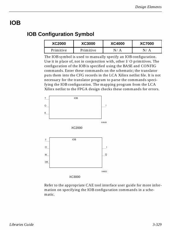
Design Elements
IOB
IOB Configuration Symbol
The IOB symbol is used to manually specify an IOB configuration.Use it in place of, not in conjunction with, other I/O primitives. Theconfiguration of the IOB is specified using the BASE and CONFIGcommands. Enter these commands on the schematic; the translatorputs them into the CFG records in the LCA Xilinx netlist file. It is notnecessary for the translator program to parse the commands speci-fying the IOB configuration. The mapping program from the LCAXilinx netlist to the FPGA design checks these commands for errors.
Refer to the appropriate CAE tool interface user guide for more infor-mation on specifying the IOB configuration commands in a sche-matic.
XC2000 XC3000 XC4000 XC7000
Primitive Primitive N/A N/A
XC2000
XC3000
X4649
K
O
T
I
IOB
X4652
OK
IK
O I
T
Q
IOB
Libraries Guide 3-329

Libraries Guide
The XC2000 blank IOB primitive symbol and its correspondingconfigured IOB primitive and circuit are shown in the followingfigure.
Figure 3-133 XC2000 IOB Primitive Example and EquivalentCircuit
X4674
TIOB
O
K
I
P12
I:Q BUF:TRI
Q
IOB P12
D
C
IFD
K
U3
PADP12
T
O
I
U2
0
U1
OBUFT
3-330 Xilinx Development System

Design Elements
The XC3000 blank IOB primitive symbol and its correspondingconfigured IOB primitive and circuit are shown in the followingfigure.
Figure 3-134 XC3000 IOB Primitive Example and EquivalentCircuit
The configuration commands must be consistent with the connec-tions to the pins on the symbol. For example, if the configurationcommands specify the IOB as a 3-state buffer, the T and O pins mustbe connected to signals.
You can specify the location of the IOB on the device. When speci-fying the LOC attribute, a valid IOB location name must be used.Refer to the “Attributes, Constraints, and Carry Logic’’ chapter formore information the LOC attribute.
X4673
TIOB
O
IK
OK
I
Q
J13
IOIN:IQ:LATCH OUT:OQ TRI:T
D
C
Q
OUTFFT
U4
D
L
INLAT
IK
U5
PADJ13
T
O
OK
I
Q
n
U2
0
Libraries Guide 3-331

Libraries Guide
IOPAD, IOPAD4, IOPAD8, and IOPAD16
Input/Output Pads
IOPAD, IOPAD4, IOPAD8, and IOPAD16 are single and multipleinput/output pads. The IOPAD is a connection point from a devicepin, used as a bidirectional signal, to a PLD device. The IOPAD isconnected internally to an input/output block (IOB), which is config-ured by the XACT software as a bidirectional block. Bidirectionalblocks can consist of any combinations of a 3-state output buffer(such as OBUFT or OFDE) and any available input buffer (such asIBUF or IFD). Refer to the appropriate CAE tool interface user guidefor details on assigning pin location and identification.
Figure 3-135 IOPAD8 XC2000/3000/4000/7000 Implementation
Name XC2000 XC3000 XC4000 XC7000
IOPAD Primitive Primitive Primitive PrimitiveIOPD4,IOPAD8,IOPAD16
Macro Macro Macro Macro
X3828
X3841
IO[7:0]
X3845
IO[15:0]
X3838
IO0
IO1
IO2
IO3
IOPAD4
IOPAD
IOPAD
IOPAD
IOPAD
IOPAD
IOPAD
IOPAD
IOPAD
IO0
IO7
IO[7:0]
IO1
IO2
IO3
IO4
IO5
IO6
3-332 Xilinx Development System
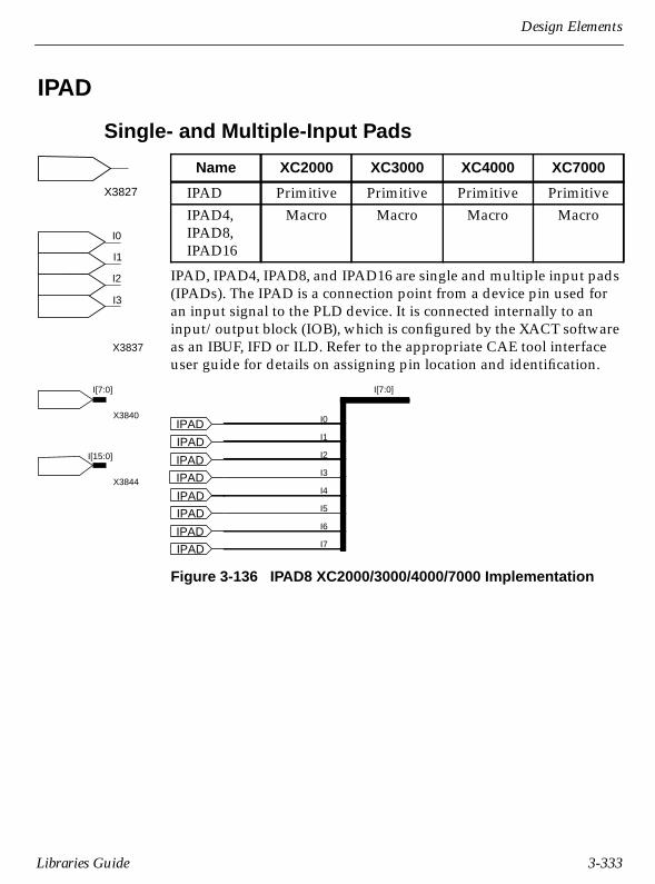
Design Elements
IPAD
Single- and Multiple-Input Pads
IPAD, IPAD4, IPAD8, and IPAD16 are single and multiple input pads(IPADs). The IPAD is a connection point from a device pin used foran input signal to the PLD device. It is connected internally to aninput/output block (IOB), which is configured by the XACT softwareas an IBUF, IFD or ILD. Refer to the appropriate CAE tool interfaceuser guide for details on assigning pin location and identification.
Figure 3-136 IPAD8 XC2000/3000/4000/7000 Implementation
Name XC2000 XC3000 XC4000 XC7000
IPAD Primitive Primitive Primitive PrimitiveIPAD4,IPAD8,IPAD16
Macro Macro Macro Macro
X3827
I0
X3837
I1
I2
I3
X3840
I[7:0]
X3844
I[15:0]
I3
I5
I0
I7
I1
I2
I4
I6
I[7:0]
IPAD
IPAD
IPAD
IPAD
IPAD
IPAD
IPAD
IPAD
Libraries Guide 3-333

Libraries Guide
LD, LD4, LD8, and LD16
Single and Multiple Transparent Data Latches
* not supported for XC7336 designs
The data output (Q) of the latch reflects the data (D) input while thegate enable (G) input is High. The data on the D input during theHigh-to-Low gate transition is stored in the latch. The data on the Qoutput remains unchanged as long as G remains Low. LD4, LD8, andLD16 have 4, 8, and 16 transparent latches, respectively, with acommon Gate enable (G).
The latch is reset, output Low, when power is applied or when globalreset (GR) is active. For EPLD designs, the G input may not be drivenby a FastCLK signal (BUFG).
d = state of input one set-up time prior to High-to-Low gate transition
Figure 3-137 LD XC2000 Implementation
Element XC2000 XC3000 XC4000 XC7000
LD Macro N/A N/A Primitive*LD4,LD8,LD16
N/A N/A N/A Primitive*
Inputs Outputs
G D Q
1 0 01 1 10 X No Chg↓ D d
Q
X3740
D LD
G
Q0
X4611
D0 LD4
G
Q1D1
Q2D2
Q3D3
Q[7:0]D[7:0]
X4612
LD8
G
Q[15:0]D[15:0]
X4613
LD16
G
LDCP
CLR
D
G
PRE Q
G
Q
GND
D
3-334 Xilinx Development System

Design Elements
LD_1
Transparent Data Latch with Inverted Gate
The data output (Q) of the latch reflects the data (D) input while thegate enable (G) input is Low. The data on the D input during theLow-to-High gate transition is stored in the latch. The data on the Qoutput remains unchanged as long as G remains High.
The latch is reset, output Low, when power is applied or when globalreset (GR) is active.
d = state of input one set-up time prior to Low-to-High gate transition
Figure 3-138 LD_1 XC2000 Implementation
XC2000 XC3000 XC4000 XC7000
Macro N/A N/A N/A
Inputs Outputs
G D Q
0 0 00 1 11 X No Chg↑ D d
Q
X3741
D LD_1
G
INV
D Q
GND
G GB
LDCP
CLR
D
G
PREQ
Libraries Guide 3-335

Libraries Guide
LDC
Transparent Data Latch with Asynchronous Clear
When the asynchronous clear input (CLR) is High, it overrides theother inputs and resets the data (Q) output Low. Q reflects the data(D) input while the gate enable (G) input is High and CLR is Low. Thedata on the D input during the High-to-Low gate transition is storedin the latch. The data on the Q output remains unchanged as long asG remains Low.
The latch is reset, output Low, when power is applied or when globalreset (GR) is active.
d = state of input one set-up time prior to High-to-Low gate transition
Figure 3-139 LDC XC2000 Implementation
XC2000 XC3000 XC4000 XC7000
Macro N/A N/A N/A
Inputs Outputs
CLR G D Q
1 X X 00 1 1 10 1 0 00 0 X No Chg0 ↓ D d
Q
X4070
D LDC
G
CLR
D Q
CLR
GND
LDCP
CLR
D
G
PREQ
G
3-336 Xilinx Development System

Design Elements
LD4CE, LD8CE, and LD16CE
Transparent Data Latches with Asynchronous Clearand Clock Enable
LD4CE, LD8CE, and LD16CE have 4, 8, and 16 transparent datalatches, respectively. When the asynchronous clear input (CLR) isHigh, it overrides the other inputs and resets the data (Q) outputsLow. Q reflects the data (D) inputs while the gate enable (G) input isHigh, clock enable (CE) is High, and CLR is Low. If CE is Low, dataon D cannot be latched. The data on the D input during the High-to-Low gate transition is stored in the latch. The data on the Q outputremains unchanged as long as G or CE remains Low.
The latch is reset, output Low, when power is applied or when globalreset (GR) is active.
Dn = referenced input, for example, D0, D1, D2
Qn = referenced output, for example, Q0, Q1, Q2
dn = referenced input state, one set-up time prior to High-to-Low gate transition
XC2000 XC3000 XC4000 XC7000
Macro N/A N/A N/A
Inputs Outputs
CLR CE G Dn Qn
1 X X X 00 0 X X No Chg0 1 1 1 10 1 1 0 00 1 0 X No Chg0 1 ↓ Dn dn
X3747
LD4CE
CLR
G
CE
D3
D2
D1
D0
Q3
Q2
Q1
Q0
X3748
LD8CE
G
CE
D[7:0]
CLR
Q[7:0]
X3749
LD16CE
G
CE
D[15:0] Q[15:0]
CLR
Libraries Guide 3-337

Libraries Guide
Figure 3-140 LD4CE XC2000 Implementation
GND
Q0
GCED Q
CLR
PRE
LDCPE
Q1
GCED Q
CLR
PRE
LDCPE
Q2
GCED Q
CLR
PRE
LDCPE
Q3
GCED Q
CLR
PRE
LDCPE
CE
D2
D1
D0
Q1
Q2
Q3
Q0
G
CLR
D3
3-338 Xilinx Development System

Design Elements
Figure 3-141 LD8CE XC2000 Implementation
GND
Q1
GCED Q
CLR
PRE
LDCPE
Q2
GCED Q
CLR
PRE
LDCPE
Q3
GCED Q
CLR
PRE
LDCPE
Q4
GCED Q
CLR
PRE
LDCPE
Q5
GCED Q
CLR
PRE
LDCPE
Q6
GCED Q
CLR
PRE
LDCPE
Q7
GCED Q
CLR
PRE
LDCPE
D[7:0]
D4
D5
D6
D7D3
D2
D1
D0
CE
Q4
Q5
Q6
Q7
Q0
Q1
Q2
Q3
Q[7:0]
CLR
Q0
GCED Q
CLR
PRE
LDCPE
G
Libraries Guide 3-339
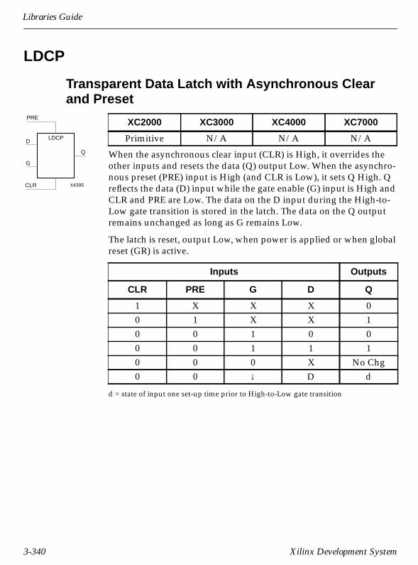
Libraries Guide
LDCP
Transparent Data Latch with Asynchronous Clearand Preset
When the asynchronous clear input (CLR) is High, it overrides theother inputs and resets the data (Q) output Low. When the asynchro-nous preset (PRE) input is High (and CLR is Low), it sets Q High. Qreflects the data (D) input while the gate enable (G) input is High andCLR and PRE are Low. The data on the D input during the High-to-Low gate transition is stored in the latch. The data on the Q outputremains unchanged as long as G remains Low.
The latch is reset, output Low, when power is applied or when globalreset (GR) is active.
d = state of input one set-up time prior to High-to-Low gate transition
XC2000 XC3000 XC4000 XC7000
Primitive N/A N/A N/A
Inputs Outputs
CLR PRE G D Q
1 X X X 00 1 X X 10 0 1 0 00 0 1 1 10 0 0 X No Chg0 0 ↓ D d
Q
D
G
LDCP
PRE
CLR X4395
3-340 Xilinx Development System

Design Elements
LDCPE
Transparent Data Latch with Asynchronous Clearand Preset and Clock Enable
When the asynchronous clear input (CLR) is High, it overrides theother inputs and resets the data (Q) output Low. When the asynchro-nous preset (PRE) input is High (and CLR is Low), it sets Q High. Qreflects the data (D) input while the gate enable (G) input and clockenable (CE) are High and CLR and PRE are Low. If CE is Low, data onD cannot be latched. The data on the D input during the High-to-Lowgate transition is stored in the latch. The data on the Q outputremains unchanged as long as G or CE remains Low.
The latch is reset, output Low, when power is applied or when globalreset (GR) is active.
d = state of input one set-up time prior to High-to-Low gate transition
XC2000 XC3000 XC4000 XC7000
Macro N/A N/A N/A
Inputs Outputs
CLR PRE CE G D Q
1 X X X X 00 1 X X X 10 0 0 X X No Chg0 0 1 1 1 10 0 1 1 0 00 0 1 0 X No Chg0 0 1 ↓ D d
Q
D
G
LDCPE
PRE
CLR X4396
CE
Libraries Guide 3-341

Libraries Guide
Figure 3-142 LDCPE XC2000 Implementation
G
DQ_D
CLR
D0D1
O
S0
M2_1
Q
CEPRE LDCP
CLR
D
G
PRE Q
3-342 Xilinx Development System
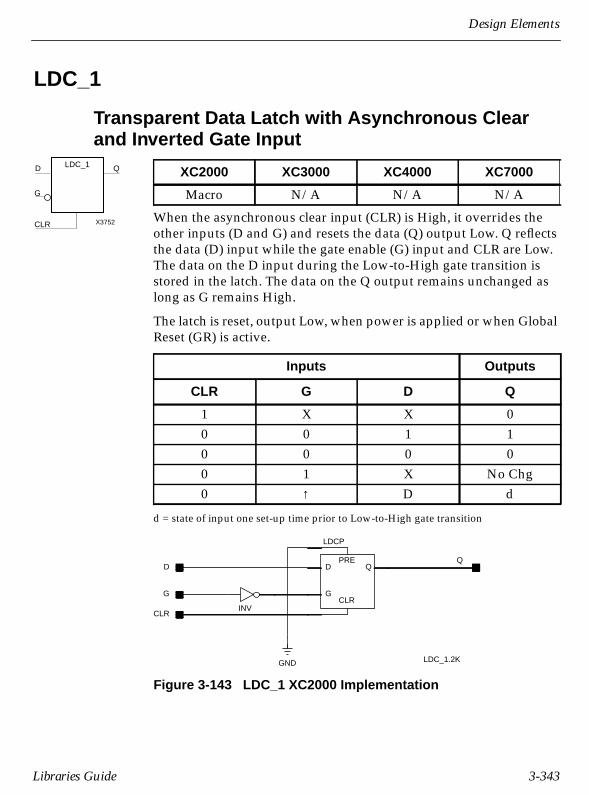
Design Elements
LDC_1
Transparent Data Latch with Asynchronous Clearand Inverted Gate Input
When the asynchronous clear input (CLR) is High, it overrides theother inputs (D and G) and resets the data (Q) output Low. Q reflectsthe data (D) input while the gate enable (G) input and CLR are Low.The data on the D input during the Low-to-High gate transition isstored in the latch. The data on the Q output remains unchanged aslong as G remains High.
The latch is reset, output Low, when power is applied or when GlobalReset (GR) is active.
d = state of input one set-up time prior to Low-to-High gate transition
Figure 3-143 LDC_1 XC2000 Implementation
XC2000 XC3000 XC4000 XC7000
Macro N/A N/A N/A
Inputs Outputs
CLR G D Q
1 X X 00 0 1 10 0 0 00 1 X No Chg0 ↑ D d
Q
X3752
D LDC_1
G
CLR
GND
D
CLR
Q
INV
G
LDC_1.2K
LDCP
CLR
D
G
PREQ
Libraries Guide 3-343

Libraries Guide
MD0
Mode 0/Input Pad Used for Readback Trigger Input
The MD0 input pad is connected to the Mode 0 (M0) input pin, whichis used to determine the configuration mode on an XC4000 device.Following configuration, MD0 can be used as an input pad, but itmust be connected through an IBUF to the user circuit. However, theuser input signal must not interfere with the device configuration.The MD0 pad cannot be used as an output pad and the IOB associ-ated with it has no flip-flop or latch. For compatibility with XC2000and XC3000 devices, this pad is usually connected to the RTRIG inputof the READBACK function.
XC2000 XC3000 XC4000 XC7000
N/A N/A Primitive N/AX3896
MD0
3-344 Xilinx Development System

Design Elements
MD1
Mode 1/Output Pad Used for Readback Data Output
The MD1 input pad is connected to the Mode 1 (M1) input pin, whichis used to determine the configuration mode on an XC4000 device.Following configuration, MD1 can be used as a 3-state or simpleoutput pad, but it must be connected through an OBUF or an OBUFTto the user circuit. However, the user output signal must not interferewith the device configuration. An MD1 pad cannot be used as aninput pad and the IOB associated with it has no flip-flop or latch. Thispad is usually connected to the DATA output of the READBACKfunction, and the output-enable input of the 3-state OBUFT isconnected to the RIP output of the READBACK function.
XC2000 XC3000 XC4000 XC7000
N/A N/A Primitive N/AX3898
MD1
Libraries Guide 3-345

Libraries Guide
MD2
Mode 2/Input Pad
The MD2 input pad is connected to the Mode 2 (M2) input pin, whichis used to determine the configuration mode on an XC4000 device.Following configuration, MD2 can be used as an input pad, but itmust be connected through an IBUF to the user circuit. However, theuser input signal must not interfere with the device configuration. AnMD2 pad cannot be used as an output pad and the IOB associatedwith it has no flip-flop or latch.
XC2000 XC3000 XC4000 XC7000
N/A N/A Primitive N/AX3900
MD2
3-346 Xilinx Development System
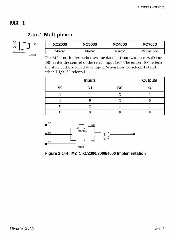
Design Elements
M2_1
2-to-1 Multiplexer
The M2_1 multiplexer chooses one data bit from two sources (D1 orD0) under the control of the select input (S0). The output (O) reflectsthe state of the selected data input. When Low, S0 selects D0 andwhen High, S0 selects D1.
Figure 3-144 M2_1 XC2000/3000/4000 Implementation
XC2000 XC3000 XC4000 XC7000
Macro Macro Macro Primitive
Inputs Outputs
S0 D1 D0 O
1 1 X 11 0 X 00 X 1 10 X 0 0
D0
D1
S0
O
X4026
AND2
OR2
AND2B1O
M0
M1
D0
D1
S0
Libraries Guide 3-347

Libraries Guide
M2_1B1
2-to-1 Multiplexer with D0 Inverted
The M2_1B1 multiplexer chooses one data bit from two sources (D1or D0) under the control of select input (S0). When S0 is Low, theoutput (O) reflects the state of D0. When S0 is High, O reflects thestate of D1.
Figure 3-145 M2_1B1 XC2000/3000/4000 Implementation
XC2000 XC3000 XC4000 XC7000
Macro Macro Macro Primitive
Inputs Outputs
S0 D1 D0 O
1 1 X 11 0 X 00 X 1 00 X 0 1
D0
D1
S0
O
X4027
S0
D1
D0
M1
M0
O
OR2
AND2
AND2B2
3-348 Xilinx Development System

Design Elements
M2_1B2
2-to-1 Multiplexer with D0 and D1 Inverted
The M2_1B2 multiplexer chooses one data bit from two sources (D1or D0) under the control of select input (S0). When S0 is Low, theoutput (O) reflects the state of D0. When S0 is High, O reflects thestate of D1.
Figure 3-146 M2_1B2 XC2000/3000/4000 Implementation
XC2000 XC3000 XC4000 XC7000
Macro Macro Macro Primitive
Inputs Outputs
S0 D1 D0 O
1 1 X 01 0 X 10 X 1 00 X 0 1
D0
D1
S0
O
X4028
OR2
O
M0
M1
D0
D1
S0
AND2B1
AND2B2
Libraries Guide 3-349

Libraries Guide
M2_1E
2-to-1 Multiplexer with Enable
When the enable input (E) is High, the M2_1E chooses one data bitfrom two sources (D1 or D0) under the control of select input (S0).When E is High, the output (O) reflects the state of the selected input.When Low, S0 selects D0 and when High, S0 selects D1. When E isLow, the output is Low.
Figure 3-147 M2_1E XC2000/3000/4000 Implementation
XC2000 XC3000 XC4000 XC7000
Macro Macro Macro Primitive
Inputs Outputs
E S0 D1 D0 O
0 X X X 01 0 X 1 11 0 X 0 01 1 1 X 11 1 0 X 0
D0
D1
S0
O
X4029E
D1
S0
D0M0
M1
O
AND3
AND3B1
OR2
E
M2_1E.2K
3-350 Xilinx Development System

Design Elements
M4_1E
4-to-1 Multiplexer with Enable
When the enable input (E) is High, the M4_1E multiplexer choosesone data bit from four sources (D3, D2, D1, or D0) under the controlof the select inputs (S1 – S0). The output (O) reflects the state of theselected input as shown in the truth table. When E is Low, the outputis Low.
XC2000 XC3000 XC4000 XC7000
Macro Macro Macro Primitive
Inputs Outputs
E S1 S0 D0 D1 D2 D3 O
0 X X X X X X 01 0 0 D0 X X X D01 0 1 X D1 X X D11 1 0 X X D2 X D21 1 1 X X X D3 D3
D0
O
X4030
D1D2D3S0S1E
Libraries Guide 3-351
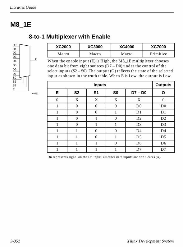
Libraries Guide
M8_1E
8-to-1 Multiplexer with Enable
When the enable input (E) is High, the M8_1E multiplexer choosesone data bit from eight sources (D7 – D0) under the control of theselect inputs (S2 – S0). The output (O) reflects the state of the selectedinput as shown in the truth table. When E is Low, the output is Low.
Dn represents signal on the Dn input; all other data inputs are don’t-cares (X).
XC2000 XC3000 XC4000 XC7000
Macro Macro Macro Primitive
Inputs Outputs
E S2 S1 S0 D7 – D0 O
0 X X X X 01 0 0 0 D0 D01 0 0 1 D1 D11 0 1 0 D2 D21 0 1 1 D3 D31 1 0 0 D4 D41 1 0 1 D5 D51 1 1 0 D6 D61 1 1 1 D7 D7
D0
O
X4031
D1D2
D7S0S1S2
D3
D4
D5
D6
E
3-352 Xilinx Development System

Design Elements
Figure 3-148 M8_1E XC2000/3000/4000 Implementation
S0
M23M01
D0
D2
D1
D4D5
D3
D6D7
M45M67
M47M03
O
S1
E
M01
D0D1
O
S0
M2_1
M23
D0D1
O
S0
M2_1
M45
D0D1
O
S0
M2_1
M67
D0D1
O
S0
M2_1
M03
D0D1
O
S0
M2_1
M47
D0D1
O
S0
M2_1
OD1D0
O
ES0
M2_1E
S2
Libraries Guide 3-353

Libraries Guide
M16_1E
16-to-1 Multiplexer with Enable
When the enable input (E) is High, the M16_1E multiplexer choosesone data bit from 16 sources (D15 – D0) under the control of the selectinputs (S3 – S0). The output (O) reflects the state of the selected inputas shown in the truth table. When E is Low, the output is Low.
Dn represents signal on the Dn input; all other data inputs are don’t-cares (X).
XC2000 XC3000 XC4000 XC7000
Macro Macro Macro Primitive
Inputs Outputs
E S3 S2 S1 S0 D15 – D0 O
0 X X X X X 01 0 0 0 0 D0 D01 0 0 0 1 D1 D11 0 0 1 0 D2 D21 0 0 1 1 D3 D3...
.
.
.
.
.
.
.
.
.
.
.
.
.
.
.
.
.
.1 1 1 0 0 D12 D121 1 1 0 1 D13 D131 1 1 1 0 D14 D141 1 1 1 1 D15 D15
D0
O
X4032
D1D2
D15
S0S1
S2
D3
D4
D5
D6
S3
D7D8D9D10D11D12D13D14
E
3-354 Xilinx Development System

Design Elements
NAND
2- to 9-Input NAND Gates with Inverted andNon-Inverted Inputs
The NAND function is performed in the Configurable Logic Block(CLB) function generators for XC2000, XC3000, and XC4000. NANDfunctions of up to five inputs are available in any combination ofinverting and non-inverting inputs. NAND functions of six to nineinputs are available with only non-inverting inputs. To invert someor all inputs, use external inverters. Since each input uses a CLBresource, replace functions with unused inputs with functions havingthe necessary number of inputs.
Figure 3-149 NAND Gate Representations
Name XC2000 XC3000 XC4000 XC7000
NAND2 – NAND4B4 Primitive Primitive Primitive PrimitiveNAND5 – NAND5B5 Macro Primitive Primitive PrimitiveNAND6 – NAND9 Macro Macro Macro Primitive
NAND9
NAND4
NAND4B3
NAND4B2
NAND4B1
NAND3B1
NAND3B2
NAND3B3
NAND2
NAND2B1
NAND2B2
NAND5
NAND5B1
NAND5B4
NAND5B3
NAND5B2
NAND4B4
NAND3
NAND6
NAND7
NAND8
NAND5B5
Libraries Guide 3-355
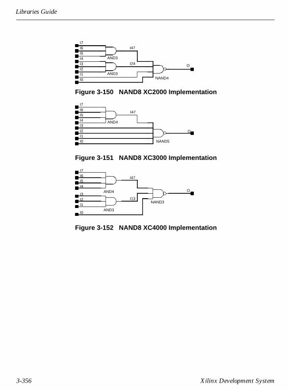
Libraries Guide
Figure 3-150 NAND8 XC2000 Implementation
Figure 3-151 NAND8 XC3000 Implementation
Figure 3-152 NAND8 XC4000 Implementation
I4
I2O
AND3I5I6I7
I47
AND3I1I0
I3 I24
NAND4
I7I6
AND4
I47
I4I5
I3I2I1I0
O
NAND5
I7
I0
I6
I3
I1I2
O
I47
I13
I4I5
AND4
AND3
NAND3
3-356 Xilinx Development System

Design Elements
NOR
2- to 9-Input NOR Gates with Inverted andNon-Inverted Inputs
The NOR function is performed in the Configurable Logic Block(CLB) function generators for XC2000, XC3000, and XC4000. NORfunctions of up to five inputs are available in any combination ofinverting and non-inverting inputs. NOR functions of six to nineinputs are available with only non-inverting inputs. To invert someor all inputs, use external inverters. Since each input uses a CLBresource, replace functions with unused inputs with functions havingthe necessary number of inputs.
Figure 3-153 NOR Gate Representations
Name XC2000 XC3000 XC4000 XC7000
NOR2 – NOR4B4 Primitive Primitive Primitive PrimitiveNOR5 – NOR5B5 Macro Primitive Primitive PrimitiveNOR6 – NOR9 Macro Macro Macro Primitive
NOR5
NOR4B3
NOR4B2
NOR4B1
NOR4
NOR3B1
NOR3B2
NOR3B3
NOR2
NOR2B1
NOR2B2NOR5B1
NOR5B2
NOR5B5
NOR5B4
NOR5B3
NOR4B4
NOR3
NOR6
NOR7
NOR8
NOR9
Libraries Guide 3-357
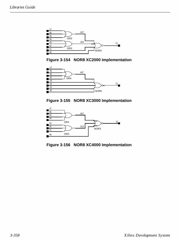
Libraries Guide
Figure 3-154 NOR8 XC2000 Implementation
Figure 3-155 NOR8 XC3000 Implementation
Figure 3-156 NOR8 XC4000 Implementation
OR3
OR3
I24I3
I0I1
I47I7I6I5
OI2
I4
NOR4
OR4
O
I0I1I2I3
I5I4
I47I6I7
NOR5
I7
I0
I6
I3
I1I2
O
I47
I13
I4I5
NOR3
OR3
OR4
3-358 Xilinx Development System

Design Elements
OBUF, OBUF4, OBUF8, and OBUF16
Single- and Multiple-Output Buffers
OBUF, OBUF4, OBUF8, and OBUF16 are single and multiple outputbuffers. An OBUF isolates the internal circuit and provides drivecurrent for signals leaving a chip. OBUFs exist in input/outputblocks (IOB). The output (O) of an OBUF is connected to an OPAD oran IOPAD. For XC7000, if a high impedance (Z) signal from anon-chip 3-state buffer (like BUFE) is applied to the input of an OBUF,it is propagated to the EPLD device output pin.
Figure 3-157 OBUF8 XC2000/3000/4000/7000 Implementation
Name XC2000 XC3000 XC4000 XC7000
OBUF Primitive Primitive Primitive PrimitiveOBUF4,OBUF8,OBUF16
Macro Macro Macro MacroX3785
X3792
OBUF4
OBUF8
X3804
OBUF16
X3816 O6
O[7:0]
O0
O1
O2
O3
O4
O5
O7
I0
I1
I2
I3
I4
I5
I6
I7
I[7:0]
OBUF
OBUF
OBUF
OBUF
OBUF
OBUF
OBUF
OBUF
Libraries Guide 3-359
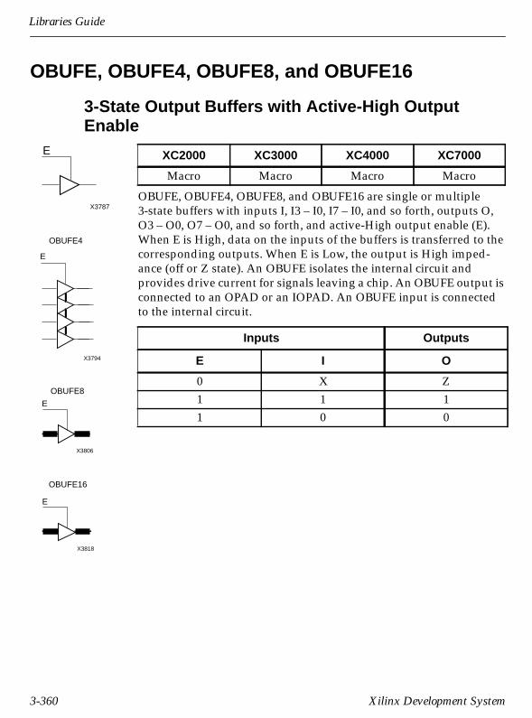
Libraries Guide
OBUFE, OBUFE4, OBUFE8, and OBUFE16
3-State Output Buffers with Active-High OutputEnable
OBUFE, OBUFE4, OBUFE8, and OBUFE16 are single or multiple3-state buffers with inputs I, I3 – I0, I7 – I0, and so forth, outputs O,O3 – O0, O7 – O0, and so forth, and active-High output enable (E).When E is High, data on the inputs of the buffers is transferred to thecorresponding outputs. When E is Low, the output is High imped-ance (off or Z state). An OBUFE isolates the internal circuit andprovides drive current for signals leaving a chip. An OBUFE output isconnected to an OPAD or an IOPAD. An OBUFE input is connectedto the internal circuit.
XC2000 XC3000 XC4000 XC7000
Macro Macro Macro Macro
Inputs Outputs
E I O
0 X Z1 1 11 0 0
X3787
E
X3794
OBUFE4
E
X3806
E
OBUFE8
OBUFE16
X3818
E
3-360 Xilinx Development System

Design Elements
Figure 3-158 OBUFE8 XC2000/3000/4000/7000 Implementation
Figure 3-159 OBUFE XC7000 Implementation
E
I[7:0]
I7
I6
I5
I4
I3
I2
I1
I0
O7
O5
O4
O3
O2
O1
O0
O[7:0]
O6E
OBUFE
E
OBUFE
E
OBUFE
E
OBUFE
E
OBUFE
E
OBUFE
E
OBUFE
E
OBUFE
I O
OBUF
EE
BUFE
Libraries Guide 3-361

Libraries Guide
OBUFEX1, OBUFE4X1, OBUFE8X1, and OBUFEX2
EPLD 3-State Output Buffers with Active-High OutputEnable
* not supported for XC7272 designs
OBUFEX1, OBUFE4X1, OBUFE8X1, and OBUFEX2 provide one, four,eight, and sixteen 3-state output buffers, respectively, with active-High output enable (E) and EPLD-style 3-state properties. OBUFEX1symbols identify signals that are driven onto EPLD device pins.When E is High, data on the inputs of the buffers is transferred to thecorresponding device outputs. When E is Low, the output is highimpedance (off or Z state). The E input can only be driven by anEPLD global Fast Output Enable (FOE) net represented by theBUFFOE symbol.
If the input (I) of an OBUFEX1 is driven by an on-chip 3-state buffer(such as BUFT), the 3-state signal is propagated through theOBUFEX1 onto the EPLD device pin, which means the output driverof the device pin is controlled by both the on-chip 3-state buffer andthe E input of the OBUFEX1. An output of an OBUFEX1 is connectedto an OPAD or an IOPAD.
Name XC2000 XC3000 XC4000 XC7000
OBUFEX1 N/A N/A N/A Primitive*OBUFE4X1,OBUFE8X1,OBUFEX2
N/A N/A N/A Macro*
Inputs Outputs
E I O
0 X Z1 1 11 0 01 Z Z
X4212
E
OBUFEX1
X4215
E
OBUFE4X1
X4218
E
I[7:0] O[7:0]
OBUFE8X1
X4221
E
OBUFEX2
I[15:0] O[15:0]
3-362 Xilinx Development System
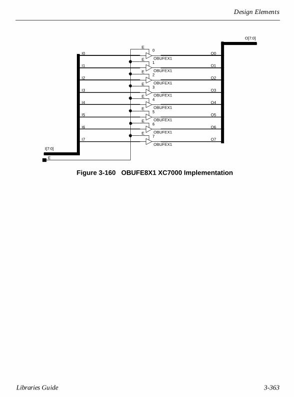
Design Elements
Figure 3-160 OBUFE8X1 XC7000 Implementation
E
I[7:0]
I7
I6
I5
I4
I3
I2
I1
I0
O7
O5
O4
O3
O2
O1
O0
O[7:0]
O6
0
OBUFEX1
E
1
OBUFEX1
E
2
OBUFEX1
E
3
OBUFEX1
E
4
OBUFEX1
E
5
OBUFEX1
E
6
OBUFEX1
E
7
OBUFEX1
E
Libraries Guide 3-363

Libraries Guide
OBUFT, OBUFT4, OBUFT8, and OBUFT16
Single and Multiple 3-State Output Buffers withActive-Low Output Enable
* not supported for XC7336 designs
OBUFT, OBUFT4, OBUFT8, and OBUFT16 are single and multiple3-state output buffers with inputs I, I3 – I0, I7 – I0, I15 – I0, outputs O,O3 – O0, O7 – O0, O15 – O0, and active-Low output enables (T).When T is Low, data on the inputs of the buffers is transferred to thecorresponding outputs. When T is High, the output is high imped-ance (off or Z state). OBUFTs isolate the internal circuit and provideextra drive current for signals leaving a chip. An OBUFT output isconnected to an OPAD or an IOPAD.
Name XC2000 XC3000 XC4000 XC7000
OBUFT Primitive Primitive Primitive Macro*OBUFT4,OBUFT8,OBUFT16
Macro Macro Macro Macro*
Inputs Outputs
T I O
1 X Z0 1 10 0 0
OBUFT
X3786
T
X3793
OBUFT4
T
OBUFT8
X3805
T
I O[8:0]
OBUFT16
X3817
T
I O[16:0]
3-364 Xilinx Development System

Design Elements
Figure 3-161 OBUFT8 XC2000/3000/4000/7000 Implementation
Figure 3-162 OBUFT XC7000 Implementation
T
I[7:0]
I7
I6
I5
I4
I3
I2
I1
I0
O7
O5
O4
O3
O2
O1
O0
O[7:0]
O6
OBUFT
T
OBUFT
T OBUFT
T
OBUFT
T OBUFT
T OBUFT
T
OBUFT
T
OBUFT
T
I O
BUFT
T
OBUF
T
Libraries Guide 3-365

Libraries Guide
OFD, OFD4, OFD8, and OFD16
Single- and Multiple-Output D Flip-Flops
OFD, OFD4, OFD8, and OFD16 are single and multiple output D flip-flops. The flip-flops exist in an input/output block (IOB) for XC3000and XC4000. The outputs (for example, Q3 – Q0) are connected toOPADs or IOPADs. The data on the D inputs is loaded into the flip-flops during the Low-to-High clock (C) transition and appears on theQ outputs.
The flip-flops are asynchronously reset, outputs Low, when power isapplied or when global reset (GR for XC3000) or global set/reset(GSR for XC4000) is active. GR is active-Low; the GSR active level isprogrammable.
dn = state of referenced input one set-up time prior to active clock transition
Name XC2000 XC3000 XC4000 XC7000
OFD N/A Primitive Primitive MacroOFD4,OFD8,OFD16
N/A Macro Macro Macro
Inputs Outputs
D C Q
D ↑ dn
Q
X3778
D OFD
C
X3800
OFD4
C
D3
D2
D1
D0
Q3
Q2
Q1
Q0
Q[7:0]
X3812
D[7:0] OFD8
C
Q[15:0]
X3834
D[15:0] OFD16
C
3-366 Xilinx Development System

Design Elements
Figure 3-163 OFD8 XC3000/4000 Implementation
Q7C
D Q
OFDQ6
C
D Q
OFDQ5
C
D Q
OFDQ4
C
D Q
OFDQ3
C
D Q
OFDQ2
C
D Q
OFDQ1
C
D Q
OFDQ0
C
D Q
OFD
Q[7:0]
Q1
Q6
Q7
Q5
Q4
Q3
Q2
Q0
C
D7
D6
D5
D0
D1
D2
D3
D4
D[7:0]
Libraries Guide 3-367

Libraries Guide
Figure 3-164 OFD8 XC7000 Implementation
Figure 3-165 OFD XC7000 Implementation
0
OBUF
Q1
FDQD
C
Q0
FDQD
C
D[7:0]
D7
D6
D5
D0
D1
D2
D3
D4
C
Q7
FDQD
C
Q6
FDQD
C
Q5
FDQD
C
Q4
FDQD
C
Q3
FDQD
C
Q2
FDQD
C
Q1
Q[7:0]
Q0
Q2
Q3
Q4
Q5
Q7
Q6
1
OBUF
2
OBUF
3
OBUF
4
OBUF
5
OBUF
6
OBUF
7
OBUF
C
O
OBUF
D Q
Q
FDQD
C
3-368 Xilinx Development System

Design Elements
OFD_1
Output D Flip-Flop with Inverted Clock
OFD_1 exists in an input/output block (IOB). The output (Q) of the Dflip-flop is connected to an OPAD or an IOPAD. The data on the Dinput is loaded into the flip-flop during the High-to-Low clock (C)transition and appears on the Q output.
The flip-flop is asynchronously reset, output Low, when power isapplied or when global reset (GR for XC2000, XC3000) or globalset/reset (GSR for XC4000) is active. GR is active-Low; the GSR activelevel is programmable.
d = state of referenced input one set-up time prior to active clock transition
Figure 3-166 OFD_1 XC3000/4000 Implementation
XC2000 XC3000 XC4000 XC7000
N/A Macro Macro N/A
Inputs Outputs
D C Q
D ↓ d
Q
X3779
D OFD_1
C
Q
C CB
D
INVC
D Q
OFD
Libraries Guide 3-369

Libraries Guide
OFDE, OFDE4, OFDE8, and OFDE16
D Flip-Flops with Active-High Enable Output Buffers
OFDE, OFDE4, OFDE8, and OFDE16 are single or multiple D flip-flops whose outputs are enabled by 3-state buffers. The flip-flop dataoutputs (Q) are connected to the inputs of output buffers (OBUFE).The OBUFE outputs (O) are connected to OPADs or IOPADs. Theseflip-flops and buffers are contained in input/output blocks (IOB) forXC3000 and XC4000. The data on the data inputs (D) is loaded intothe flip-flops during the Low-to-High clock (C) transition. When theactive-High enable inputs (E) are High, the data on the flip-flopoutputs (Q) appears on the O outputs. When E is Low, outputs arehigh impedance (Z state or off).
The flip-flops are asynchronously reset, outputs Low, when power isapplied or when global reset (GR for XC3000) or global set/reset(GSR for XC4000) is active. GR is active-Low; the GSR active level isprogrammable.
Name XC2000 XC3000 XC4000 XC7000
OFDE N/A Macro Macro MacroOFDE4,OFDE8,OFDE16
N/A Macro Macro Macro
Inputs Outputs
E D C O
0 X X Z, not off1 1 ↑ 11 0 ↑ 0
Q
X3782
D OFDE
E
C
X3802
OFDE4
C
D3
D2
D1
D0 Q0
Q1
Q2
Q3
E
Q[7:0]
X3814
D[7:0] OFDE8
C
E
Q[15:0]
X3836
D[15:0] OFDE16
C
E
3-370 Xilinx Development System

Design Elements
Figure 3-167 OFDE XC7000 Implementation
Figure 3-168 OFDE8 XC3000/4000 Implementation
E
Q
FDQD
C
OD
C
O
OBUFE
E
O6
D
C
Q
OFDEE
O5
D
C
Q
OFDEE
O4
D
C
Q
OFDEE
O3
D
C
Q
OFDEE
O2
D
C
Q
OFDEE
O1
D
C
Q
OFDEE
O0
D
C
Q
OFDEE
CE
D[7:0] D7
D5
D0
D1
D2
D3
D4
D6
O[7:0]
O7
O6
O5
O4
O3
O2
O1
O0
O7
D
C
Q
OFDEE
Libraries Guide 3-371

Libraries Guide
Figure 3-169 OFDE8 XC7000 Implementation
O0
O7
O6
O5
O4
O3
O2
O[7:0]
O1
E
Q2
FDQD
C
Q3
FDQD
C
Q4
FDQD
C
Q5
FDQD
C
Q6
FDQD
C
Q7
FDQD
C
C
D4
D3
D2
D1
D0
D5
D6
D7
D[7:0]
Q0
FDQD
C
Q1
FDQD
C
7
OBUFE
E
6
OBUFE
E
5
OBUFE
E
4
OBUFE
E
3
OBUFE
E
2
OBUFE
E
1
OBUFE
E
0
OBUFE
E
3-372 Xilinx Development System

Design Elements
OFDE_1
D Flip-Flop with Active-High Enable Output Bufferand Inverted Clock
OFDE_1 and its output buffer exist in an input/output block (IOB).The data output of the flip-flop (Q) is connected to the input of anoutput buffer or OBUF. The output of the OBUF is connected to anOPAD or an IOPAD. The data on the data input (D) is loaded into theflip-flop on the High-to-Low clock (C) transition. When the active-High enable input (E) is High, the data on the flip-flop output (Q)appears on the O output. When E is Low, the output is high imped-ance (Z state or off).
The flip-flop is asynchronously reset, output Low, when power isapplied or when global reset (GR for XC3000) or global set/reset(GSR for XC4000) is active. GR is active-Low; the GSR active level isprogrammable.
Figure 3-170 OFDE_1 XC3000/4000 Implementation
XC2000 XC3000 XC4000 XC7000
N/A Macro Macro N/A
Inputs Outputs
E D C O
0 X X Z1 1 ↓ 11 0 ↓ 0
Q
X3783
D OFDE_1
E
C
INV
Q
C
D
OFDT
OD
T
INV
E
CBC
Libraries Guide 3-373

Libraries Guide
OFDEI
D Flip-Flop with Active-High Enable Output Buffer(Asynchronous Set)
OFDEI is a D flip-flop whose output is enabled by a 3-state buffer.The data output (Q) of the flip-flop is connected to the input of anoutput buffer or OBUF. The output of the OBUF (O) is connected toan OPAD or an IOPAD. These flip-flops and buffers are contained ininput/output blocks (IOB). The data on the data input (D) is loadedinto the flip-flop during the Low-to-High clock (C) transition. Whenthe active-High enable input (E) is High, the data on the flip-flopoutput (Q) appears on the O output. When E is Low, the output ishigh impedance (Z state or off). The flip-flop is asynchronously set,output High, when power is applied or when global set/reset (GSR)is active. The GSR active level is programmable.
Figure 3-171 OFDEI XC4000 Implementation
XC2000 XC3000 XC4000 XC7000
N/A N/A Macro N/A
Inputs Outputs
E D C O
0 X X Z1 1 ↑ 11 0 ↑ 0
Q
X4382
D OFDEI
E
C
E
D
C
T
INV O
C
D Q
OFDTI
OFDEI.4K
3-374 Xilinx Development System
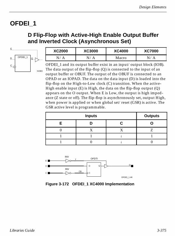
Design Elements
OFDEI_1
D Flip-Flop with Active-High Enable Output Bufferand Inverted Clock (Asynchronous Set)
OFDEI_1 and its output buffer exist in an input/output block (IOB).The data output of the flip-flop (Q) is connected to the input of anoutput buffer or OBUF. The output of the OBUF is connected to anOPAD or an IOPAD. The data on the data input (D) is loaded into theflip-flop on the High-to-Low clock (C) transition. When the active-High enable input (E) is High, the data on the flip-flop output (Q)appears on the O output. When E is Low, the output is high imped-ance (Z state or off). The flip-flop is asynchronously set, output High,when power is applied or when global set/reset (GSR) is active. TheGSR active level is programmable.
Figure 3-172 OFDEI_1 XC4000 Implementation
XC2000 XC3000 XC4000 XC7000
N/A N/A Macro N/A
Inputs Outputs
E D C O
0 X X Z1 1 ↓ 11 0 ↓ 0
Q
X4383
D OFDEI_1
E
C
C
D Q
OFDTI
INV
OD
TINV
E
CBC
OFDEI_1.4K
Libraries Guide 3-375

Libraries Guide
OFDI
Output D Flip-Flop (Asynchronous Set)
OFDI is contained in an input/output block (IOB). The output (Q) ofthe D flip-flop is connected to an OPAD or an IOPAD. The data on theD input is loaded into the flip-flop during the Low-to-High clock (C)transition and appears at the output (Q).
The flip-flop is asynchronously set, output High, when power isapplied or when global set/reset (GSR) is active. The GSR active levelis programmable.
d = state of referenced input one set-up time prior to active clock transition
XC2000 XC3000 XC4000 XC7000
N/A N/A Primitive N/A
Inputs Outputs
D C Q
D ↑ d
Q
X4582
D OFDI
C
3-376 Xilinx Development System
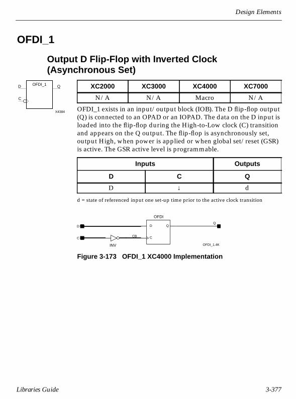
Design Elements
OFDI_1
Output D Flip-Flop with Inverted Clock(Asynchronous Set)
OFDI_1 exists in an input/output block (IOB). The D flip-flop output(Q) is connected to an OPAD or an IOPAD. The data on the D input isloaded into the flip-flop during the High-to-Low clock (C) transitionand appears on the Q output. The flip-flop is asynchronously set,output High, when power is applied or when global set/reset (GSR)is active. The GSR active level is programmable.
d = state of referenced input one set-up time prior to the active clock transition
Figure 3-173 OFDI_1 XC4000 Implementation
XC2000 XC3000 XC4000 XC7000
N/A N/A Macro N/A
Inputs Outputs
D C Q
D ↓ d
Q
X4384
D OFDI_1
C
C
D Q
OFDI
Q
CCB
D
INV OFDI_1.4K
Libraries Guide 3-377

Libraries Guide
OFDT, OFDT4, OFDT8, and OFDT16
Single and Multiple D Flip-Flops with Active-High3-State Active-Low Output Enable Buffers
* not supported for XC7336 designs
OFDT, OFDT4, OFDT8, and OFDT16 are single or multiple D flip-flops whose outputs are enabled by a 3-state buffers. The dataoutputs (Q) of the flip-flops are connected to the inputs of outputbuffers (OBUFT). The outputs of the OBUFTs (O) are connected toOPADs or IOPADs. These flip-flops and buffers exist in input/outputblocks (IOB) for XC3000 and XC4000. The data on the data inputs (D)is loaded into the flip-flops during the Low-to-High clock (C) transi-tion. When the active-Low enable inputs (T) are Low, the data on theflip-flop outputs (Q) appears on the O outputs. When T is High,outputs are high impedance (off).
The flip-flops are asynchronously reset, outputs Low, when power isapplied or when global reset (GR for XC3000) or global set/reset(GSR for XC4000) is active. GR is active-Low; the GSR active level isprogrammable.
d = state of referenced input one set-up time prior to active clock transition
Name XC2000 XC3000 XC4000 XC7000
OFDT N/A Primitive Primitive Macro*OFDT4,OFDT8,OFDT16
N/A Macro Macro Macro*
Inputs Outputs
T D C O
1 X X Z0 D ↑ d
Q
X3780
D OFDT
C
T
X3801
OFDT4
C
D3
D2
D1
D0 Q0
Q1
Q2
Q3
T
Q[7:0]
X3813
D[7:0] OFDT8
C
T
Q[15:0]
X3835
D[15:0] OFDT16
C
T
3-378 Xilinx Development System
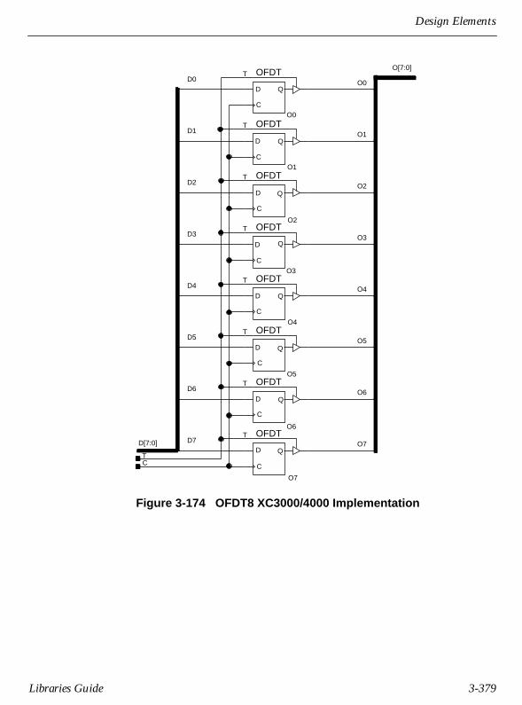
Design Elements
Figure 3-174 OFDT8 XC3000/4000 Implementation
TC
D[7:0] D7
D5
D0
D1
D2
D3
D4
D6
O[7:0]
O7
O6
O5
O4
O3
O2
O1
O0
O7
Q
C
D
OFDTTO6
Q
C
D
OFDTTO5
Q
C
D
OFDTTO4
Q
C
D
OFDTTO3
Q
C
D
OFDTTO2
Q
C
D
OFDTTO1
Q
C
D
OFDTT
O0
Q
C
D
OFDTT
Libraries Guide 3-379

Libraries Guide
Figure 3-175 OFDT8 XC7000 Implementation
Figure 3-176 OFDT XC7000 Implementation
0
OBUFT
T
1
OBUFT
T
2
OBUFT
T
3
OBUFT
T
4
OBUFT
T
5
OBUFT
T
6
OBUFT
T
7
OBUFT
T
Q1
FD
QD
C
Q0
FD
QD
C
D[7:0]
D7
D6
D5
D0
D1
D2
D3
D4
C
Q7
FD
QD
C
Q6
FD
QD
C
Q5
FD
QD
C
Q4
FD
QD
C
Q3
FD
QD
C
Q2
FD
QD
C
T
O1
O[7:0]
O2
O3
O4
O5
O6
O7
O0
O
OBUFT
T
C
D O
Q
FD
QD
C
T
3-380 Xilinx Development System

Design Elements
OFDT_1
D Flip-Flop with Active-High 3-State and Active-LowOutput Buffer and Inverted Clock
OFDT_1 and its output buffer exist in an input/output block (IOB).The flip-flop data output (Q) is connected to the input of an outputbuffer (OBUF). The OBUF output is connected to an OPAD or anIOPAD. The data on the data input (D) is loaded into the flip-flop onthe High-to-Low clock (C) transition. When the active-Low enableinput (T) is Low, the data on the flip-flop output (Q) appears on the Ooutput. When T is High, the output is high impedance (off).
The flip-flop is asynchronously reset, output Low, when power isapplied or when global reset (GR for XC3000) or global set/reset(GSR for XC4000) is active. GR is active-Low; the GSR active level isprogrammable.
Figure 3-177 OFDT_1 XC3000/4000 Implementation
XC2000 XC3000 XC4000 XC7000
N/A Macro Macro N/A
Inputs Outputs
T D C O
1 X X Z0 1 ↓ 10 0 ↓ 0
Q
X3781
D OFDT_1
T
C
INV
OD
CBC
Q
C
D
OFDTTT
Libraries Guide 3-381

Libraries Guide
OFDTI
D Flip-Flop with Active-High 3-State and Active-LowOutput Buffer (Asynchronous Set)
OFDTI and its output buffer are contained in an input/output block(IOB). The data output of the flip-flop (Q) is connected to the input ofan output buffer (OBUF). The output of the OBUF is connected to anOPAD or an IOPAD. The data on the data input (D) is loaded into theflip-flop on the Low-to-High clock (C) transition. When the active-Low enable input (T) is Low, the data on the flip-flop output (Q)appears on the output (O). When T is High, the output is high imped-ance (off).
The flip-flop is asynchronously set, output High, when power isapplied or when global set/reset (GSR) is active. The GSR active levelis programmable.
XC2000 XC3000 XC4000 XC7000
N/A N/A Primitive N/A
Inputs Outputs
T D C O
1 X X Z0 1 ↑ 10 0 ↑ 0
Q
X4581
D OFDTI
C
T
3-382 Xilinx Development System

Design Elements
OFDTI_1
D Flip-Flop with Active-High 3-State, Active-LowOutput Buffer and Inverted Clock
OFDTI_1 and its output buffer are contained in an input/outputblock (IOB). The data output of the flip-flop (Q) is connected to theinput of an output buffer (OBUF). The OBUF output is connected toan OPAD or an IOPAD. The data on the data input (D) is loaded intothe flip-flop on the High-to-Low clock (C) transition. When theactive-Low enable input (T) is Low, the data on the flip-flop output(Q) appears on the O output. When T is High, the output is highimpedance (off).
The flip-flop is asynchronously set, output High, when power isapplied or when global set/reset (GSR) is active. The GSR active levelis programmable.
Figure 3-178 OFDTI_1 XC4000 Implementation
XC2000 XC3000 XC4000 XC7000
N/A N/A Macro N/A
Inputs Outputs
T D C O
1 X X Z0 1 ↓ 10 0 ↓ 0
Q
X4385
D OFDTI_1
T
C
INV
OD
CBC
T
C
D
T
Q
OFDTI
OFDTI_1.4K
Libraries Guide 3-383

Libraries Guide
OPAD, OPAD4, OPAD8, and OPAD16
Single- and Multiple-Output Pads
OPAD, OPAD4, OPAD8, and OPAD16 are single and multiple outputpads. An OPAD connects a device pin to an output signal of a PLD. Itis internally connected to an input/output block (IOB), which isconfigured by the XACT software as an OBUF, an OBUFT, an OBUFE,an OFD, or an OFDT.
Refer to the appropriate CAE tool interface user guide for details onassigning pin location and identification.
Figure 3-179 OPAD8 XC2000/3000/4000 Implementation
Name XC2000 XC3000 XC4000 XC7000
OPAD Primitive Primitive Primitive PrimitiveOPAD4,OPAD8,OPAD16
Macro Macro Macro Macro
O0
X3839
OPAD4
O1
O2
O3
X3842
OPAD8
O[7:0]
X3846
OPAD16
O[15:0]
X3829
OPAD
O[7:0]
O1
O0
O3
O5
O7
O6
O4
O2
OPAD
OPAD
OPAD
OPAD
OPAD
OPAD
OPAD
OPAD
3-384 Xilinx Development System
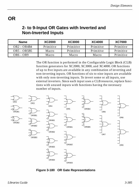
Design Elements
OR
2- to 9-Input OR Gates with Inverted andNon-Inverted Inputs
The OR function is performed in the Configurable Logic Block (CLB)function generators for XC2000, XC3000, and XC4000. OR functionsof up to five inputs are available in any combination of inverting andnon-inverting inputs. OR functions of six to nine inputs are availablewith only non-inverting inputs. To invert some or all inputs, useexternal inverters. Since each input uses a CLB resource, replace func-tions with unused inputs with functions having the necessarynumber of inputs.
Figure 3-180 OR Gate Representations
Name XC2000 XC3000 XC4000 XC7000
OR2 – OR4B4 Primitive Primitive Primitive PrimitiveOR5 – OR5B5 Macro Primitive Primitive PrimitiveOR6 – OR9 Macro Macro Macro Primitive
OR4
OR4B3
OR4B2
OR4B1
OR3B1
OR3B2
OR3B3
OR2
OR2B1
OR2B2
OR5
OR5B1
OR5B2
OR5B3
OR5B5
OR5B4
OR4B4
OR3
OR6
OR7
OR9
OR8
Libraries Guide 3-385

Libraries Guide
Figure 3-181 OR8 XC2000 Implementation
Figure 3-182 OR8 XC3000 Implementation
Figure 3-183 OR8 XC4000 Implementation
I4
I2O
I5I6I7
I47
I1I0
I3 I24
OR3
OR3
OR4
I7I6 I47
I4I5
I3I2I1I0
O
OR4
OR5
I7I6
I4I5
I1I2I3
I0
I13
I47
O
OR3
OR3
OR4
3-386 Xilinx Development System
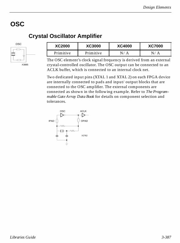
Design Elements
OSC
Crystal Oscillator Amplifier
The OSC element’s clock signal frequency is derived from an externalcrystal-controlled oscillator. The OSC output can be connected to anACLK buffer, which is connected to an internal clock net.
Two dedicated input pins (XTAL 1 and XTAL 2) on each FPGA deviceare internally connected to pads and input/output blocks that areconnected to the OSC amplifier. The external components areconnected as shown in the following example. Refer to The Program-mable Gate Array Data Book for details on component selection andtolerances.
XC2000 XC3000 XC4000 XC7000
Primitive Primitive N/A N/A
X3885
OSC
OSC
X2762
IPAD OPAD
ACLK
Libraries Guide 3-387

Libraries Guide
OSC4
Internal 5-Frequency Clock-Signal Generator
OSC4 provides internal clock signals in applications where timing isnot critical. The available frequencies are determined by FPGA devicecomponents, which are process dependent. Therefore, the availablefrequencies vary from device to device. Nominal frequencies are 8MHz, 500 KHz, 16 KHz, 490 Hz, and 15 Hz. Although there are fiveoutputs, only three can be used at a time, with 8 MHz on one outputand one frequency each on any two of the remaining four outputs. Anerror occurs if more than three outputs are used simultaneously. Theinternal circuit must be connected through buffers to OSC4 outputs.
XC2000 XC3000 XC4000 XC7000
N/A N/A Primitive N/A
X3912
F15
OSC4
F490
F16K
F500K
F8M
3-388 Xilinx Development System
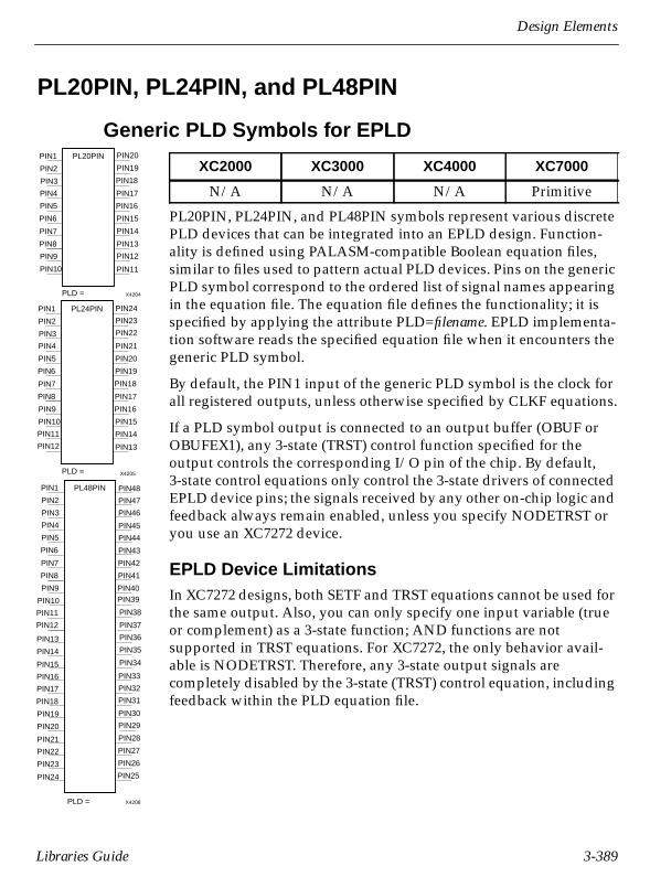
Design Elements
PL20PIN, PL24PIN, and PL48PIN
Generic PLD Symbols for EPLD
PL20PIN, PL24PIN, and PL48PIN symbols represent various discretePLD devices that can be integrated into an EPLD design. Function-ality is defined using PALASM-compatible Boolean equation files,similar to files used to pattern actual PLD devices. Pins on the genericPLD symbol correspond to the ordered list of signal names appearingin the equation file. The equation file defines the functionality; it isspecified by applying the attribute PLD=filename. EPLD implementa-tion software reads the specified equation file when it encounters thegeneric PLD symbol.
By default, the PIN1 input of the generic PLD symbol is the clock forall registered outputs, unless otherwise specified by CLKF equations.
If a PLD symbol output is connected to an output buffer (OBUF orOBUFEX1), any 3-state (TRST) control function specified for theoutput controls the corresponding I/O pin of the chip. By default,3-state control equations only control the 3-state drivers of connectedEPLD device pins; the signals received by any other on-chip logic andfeedback always remain enabled, unless you specify NODETRST oryou use an XC7272 device.
EPLD Device LimitationsIn XC7272 designs, both SETF and TRST equations cannot be used forthe same output. Also, you can only specify one input variable (trueor complement) as a 3-state function; AND functions are notsupported in TRST equations. For XC7272, the only behavior avail-able is NODETRST. Therefore, any 3-state output signals arecompletely disabled by the 3-state (TRST) control equation, includingfeedback within the PLD equation file.
XC2000 XC3000 XC4000 XC7000
N/A N/A N/A Primitive
X4204
PL20PIN
PLD =
PIN8
PIN10
PIN9
PIN7
PIN4
PIN6
PIN5
PIN1
PIN3
PIN2
PIN13
PIN16
PIN14
PIN15
PIN17
PIN20
PIN18
PIN19
PIN11
PIN12
PIN15
X4208
PL48PIN
PLD =
PIN8
PIN10
PIN9
PIN7
PIN4
PIN6
PIN5
PIN1
PIN3
PIN2
PIN42
PIN40
PIN41
PIN43
PIN46
PIN11
PIN12 PIN37
PIN38
PIN34
PIN35
PIN36
PIN47
PIN13
PIN14
PIN16
PIN44
PIN45
PIN48
PIN18
PIN17
PIN21
PIN20
PIN19
PIN24
PIN23
PIN22 PIN27
PIN25
PIN26
PIN28
PIN31
PIN32
PIN29
PIN30
PIN33
PIN39
X4205
PL24PIN
PLD =
PIN8
PIN10
PIN9
PIN7
PIN4
PIN6
PIN5
PIN1
PIN3
PIN2
PIN13
PIN16
PIN14
PIN15
PIN17
PIN20
PIN18
PIN19
PIN21
PIN22
PIN11
PIN12
PIN23
PIN24
Libraries Guide 3-389

Libraries Guide
PL20V8
20V8-Compatible PLD Symbol for EPLD
The PL20V8 symbol represents a GAL20V8 PLD covering all 24-pinmedium PAL devices. Functionality is defined using the samePALASM-compatible Boolean equation file or GAL20V8 JEDECprogramming file used to pattern an actual GAL or PAL device. Pinson the PL20V8 symbol correspond to the ordered list of signal namesappearing in the equation file (or JEDEC file). You can specify theequation file used to define the functionality by applying the attributePLD=filename. EPLD implementation software reads the specifiedequation file when it encounters the PL20V8 symbol.
GAL20V8-Compatible FunctionalityGenerally, the PL20V8 produces up to eight output functions. You cansynchronize each output with a D-type flip-flop. Flip-flops are trig-gered on the rising edge of the clock signal. By default, the PIN1input is the clock for all registers. You can invert each output.
Each output has 3-state drive capability. If the output is connected toan output buffer (OBUF or OBUFEX1), the corresponding 3-state I/Opin is controlled by the PL20V8 output-enable control input, PIN 13,or a 3-state (TRST) control equation. By default, each output specifiedby a non-registered equation is always enabled, and each registeredoutput is enabled when the PIN13 input is Low, which makes itcompatible with 24-pin medium PAL devices. Unused output pinsare always disabled to allow these pins to be reused as inputs. Asingle product term can be used to control the output enable of eachoutput (pins 15 – 22) through the 3-state (TRST) control equation.
The defaults mentioned in the previous paragraphs override thenormal defaults for the Xilinx PLUSASM equation language whenPL20V8 is the specified PLD component type.
XC2000 XC3000 XC4000 XC7000
N/A N/A N/A Primitive
X4202
PL20V8
PLD =
PIN8
PIN10
PIN9
PIN7
PIN4
PIN6
PIN5
PIN1
PIN3
PIN2
PIN13
PIN16
PIN14
PIN15
PIN17
PIN20
PIN18
PIN19
PIN23
PIN21
PIN22
PIN11
3-390 Xilinx Development System

Design Elements
GAL20V8 ExceptionsBy default, the output enable controls of a PL20V8 control only the3-state drivers of the EPLD device pins, not the signals received byany other on-chip logic. For example, if a 3-state control equation isspecified and the corresponding output only connects to otheron-chip logic symbols, the 3-state equation has no effect. You canoverride this default by using the PLUSASM NODETRST declarationin your equation file. When NODETRST is specified, the outputsignal is disabled by the 3-state control equation everywhere it occursin the design, including feedback within the PL20V8 equation file.
Extended FunctionalityAs an alternative to using the default clock, PIN1, you can take asingle product term from each registered output function and use itas the clock source (logic-controlled clocking) by specifying a CLKFcontrol equation in your equation file.
You can synchronously set and/or reset each output register usingsingle product-term functions. You can take a single product termfrom each output to control the register set or reset by specifying theSETF or the RSTF control equation. The register is forced High orLow while the set or reset product term is satisfied.
When the EPLD device is powered up or its Master Reset pin is acti-vated, all registers in the device are initialized. You can select theinitial state of each PL20V8 output flip-flop using the PLUSASMPRLD control equation. Polarity inversion is performed before theD-input to the flip-flop, making the results of reset, set, and pre-loading (power on or Master Reset) on the outputs independent ofselected polarity.
You can override the default 3-state control of registered outputsthrough PIN 13 by specifying the control equationoutput•TRST=VCC in the equation file for each output. Overridingthe default forces the output to always be enabled, allows PIN13 to beused as an ordinary logic input, and allows the associated productterm to be used as part of the output logic-defining function.
Libraries Guide 3-391

Libraries Guide
Pin DescriptionPIN1 is the default clock input. It triggers all registers on the Low-to-High transition and can be driven by a FastCLK global net (BUFGsymbol). Only the PIN1 input can be driven by a FastCLK global net.If it is driven by a FastCLK net, the signal cannot be used in any equa-tions in the PLD. PIN1 can be used as a general-purpose logic input ifit is not driven by a FastCLK.
PIN2 – PIN11, PIN14, and PIN23 are general-purpose logic inputs.
PIN13 is the default active-Low output-enable control input for regis-tered outputs. Outputs are enabled while pin 13 is Low. Pin 13 canalso be used as an ordinary logic input.
PIN15 – PIN22 are logic function outputs with optional 3-statecontrol. These pins can be used as ordinary logic inputs when nocorresponding output function is specified.
PIN12 and PIN24 are not shown on the PL20V8 symbol, because theyare the ground and VCC pins.
EPLD Device LimitationsIn XC7272 designs, both SETF and TRST equations cannot be used forthe same output. Also, only one input variable (true or complement)can be specified as a 3-state function; AND functions are notsupported in TRST equations. For XC7272, only the NODETRSTbehavior is available. Therefore, any 3-state output signals arecompletely disabled by the 3-state control equation (or pin 13 forregistered outputs), including feedback within the PL20V8 equationfile.
3-392 Xilinx Development System

Design Elements
PL22V10
22V10-Compatible PLD Symbol for EPLD
The PL22V10 symbol represents a PAL22V10 PLD. Functionality isdefined using the same PALASM-compatible Boolean equation file orPAL22V10 JEDEC programming file used to pattern an actualPAL22V10 device. The pins on the PL22V10 symbol correspond to theordered list of signal names appearing in the equation file (or JEDECfile). Specify the equation file by applying the attribute PLD=filename.EPLD implementation software reads the specified equation filewhen it encounters the PL22V10 symbol.
PAL22V10-Compatible FunctionalityGenerally, the PL22V10 produces up to 10 output functions. You cansynchronize each output with a D-type flip-flop. Flip-flops are trig-gered on the rising edge of the clock signal. By default, the PIN1input is the clock for all registers.
Each output has 3-state drive capability. If the output is connected toan output buffer (OBUF or OBUFEX1), the corresponding 3-state I/Opin is controlled by the PL22V10 output-enable (TRST) control equa-tion. By default, each output equation is always enabled. UnusedPL22V10 output pins are always disabled, allowing the symbol pin tobe re-used as an input. You can use a single product term to controlthe output enable of each output through the 3-state control equation.
You can implement global asynchronous reset by specifying a signalname in the 25th pin position in the equation file and by applying aRSTF control equation that is compatible with PALASM syntax forthe PAL22V10 architecture. Implementing global asynchronous resetcauses the EPLD implementation software to automatically replicatethe reset function on each of the outputs' reset product terms. Allregisters are forced Low while the global asynchronous reset functionis satisfied.
Similarly, you can implement global synchronous preset by speci-fying a signal name in the 25th pin position in the equation file andby applying a SETF control equation. Implementing global synchro-
XC2000 XC3000 XC4000 XC7000
N/A N/A N/A Primitive
X4203
PL22V10
PLD =
PIN8
PIN10
PIN9
PIN7
PIN4
PIN6
PIN5
PIN1
PIN3
PIN2
PIN13
PIN16
PIN14
PIN15
PIN17
PIN20
PIN18
PIN19
PIN23
PIN21
PIN22
PIN11
Libraries Guide 3-393
Libraries Guide
nous preset causes the EPLD implementation software to automati-cally replicate it into each of the registered output logic functions. Allregisters are forced High synchronously with the clock, if the globalsynchronous preset function is satisfied.
Individual output SETF and RSTF control equations are notsupported for PL22V10 equation files.
Each output can be inverted. EPLD software automatically emulatesPAL22V10 architecture by applying logic inversions to the Q-outputof the flip-flop. The results of asynchronous reset, synchronouspreset, and pre-loading (power-on) at the outputs are reversed as aresult of selecting active-Low output polarity.
The defaults mentioned in the previous paragraphs override thenormal defaults for the Xilinx PLUSASM equation language whenPL22V10 is the specified PLD component type.
PAL22V10 ExceptionsOutput-enable controls, by default, only control EPLD device pin3-state drivers, not signals received by any other on-chip logic. Forexample, if you specify a 3-state control equation and the corre-sponding output only connects to other on-chip logic symbols, the3-state equation has no effect. You can override this default using thePLUSASM NODETRST declaration in your equation file. WhenNODETRST is specified, the output signal is disabled by the 3-statecontrol equation everywhere it occurs, including feedback within thePL22V10 equation file.
Extended FunctionalityAs an alternative to using the default clock, PIN1, you can take asingle product term from each registered output function and use itas the clock source (logic-controlled clocking) by specifying a CLKFcontrol equation in your equation file.
3-394 Xilinx Development System

Design Elements
When the EPLD device is powered up or its Master Reset pin is acti-vated, all registers in the device are initialized. You can select theinitial state of each PL22V10 output flip-flop using the PLUSASMPRLD control equation.
Pin DescriptionPIN1, the default clock input, triggers all registers on the Low-to-High transition. It can be driven by a FastCLK global net (BUFGsymbol). Only the PIN1 input can be driven by a FastCLK global net.If it is driven by a FastCLK net, the signal on PIN1 cannot be used inany equations in the PLD. PIN1 can be used as a general-purposelogic input if it is not driven by a FastCLK.
PIN2 – PIN11 and PIN13 are general-purpose logic inputs.
PIN14 – PIN23 are logic function outputs with optional 3-statecontrol. These pins can be used as ordinary logic inputs when nocorresponding output function is specified.
PIN12 and PIN24 are not shown on the PL22V10 symbol, becausethey are the ground and VCC pins.
EPLD Device LimitationsIn XC7272 designs, 3-state control equations cannot be used if anasynchronous reset function is also specified. You can only specifyone input variable (true or complement) as a 3-state function; ANDfunctions are not supported in TRST equations. Only the NODETRSTbehavior is available for XC7272. Therefore, any 3-state outputsignals are completely disabled by the 3-state control equation,including feedback within the PL22V10 equation file.
Libraries Guide 3-395

Libraries Guide
PLFB9
EPLD High-Density Function Block PLD Symbol
* not supported for XC7336 designs
PLFB9 is a Xilinx-proprietary PLD configuration with all the logicand macrocell resources available in a Xilinx EPLD High-DensityFunction Block. Its features are a superset of various discrete PLDproducts, including medium PAL devices and registered-asynchro-nous devices, such as PAL20RA10.
Specify custom logic functions using the Xilinx PLUSASM Booleanequation language in a syntax upwardly compatible with the popularPALASM Boolean equation language. PLFB9 pins correspond to theordered list of signal names appearing in the equation file. The equa-tion file used to define the functionality is specified by applying theattribute PLD=filename. EPLD implementation software reads thisequation file when it encounters the PLFB9 symbol in the schematic.(For equivalent logic of XC7272 macrocells, consult the device datasheet.)
XC2000 XC3000 XC4000 XC7000
N/A N/A N/A Primitive*
PIN15
X4206
PLFB9
PLD =
PIN8
PIN10
PIN9
PIN7
PIN4
PIN6
PIN5
PIN1
PIN3
PIN2
PIN23
PIN24
PIN27
PIN25
PIN26
PIN28
PIN29
PIN11
PIN12
PIN20
PIN21
PIN22
PIN17
PIN18
PIN19
PIN16
PIN30
CO
PIN13
PIN14
PIN32
PIN31
CI
3-396 Xilinx Development System
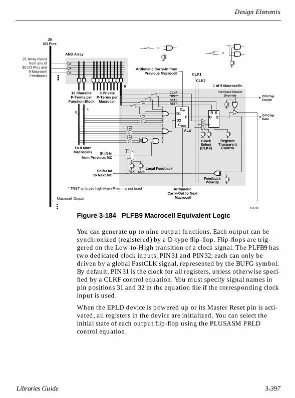
Design Elements
Figure 3-184 PLFB9 Macrocell Equivalent Logic
You can generate up to nine output functions. Each output can besynchronized (registered) by a D-type flip-flop. Flip-flops are trig-gered on the Low-to-High transition of a clock signal. The PLFB9 hastwo dedicated clock inputs, PIN31 and PIN32; each can only bedriven by a global FastCLK signal, represented by the BUFG symbol.By default, PIN31 is the clock for all registers, unless otherwise speci-fied by a CLKF control equation. You must specify signal names inpin positions 31 and 32 in the equation file if the corresponding clockinput is used.
When the EPLD device is powered up or its Master Reset pin is acti-vated, all registers in the device are initialized. You can select theinitial state of each output flip-flop using the PLUSASM PRLDcontrol equation.
Clock Select (CLKF)
Register Trasparent
Control
Local Feedback
Arithmetic Carry-Out to Next
Macrocell
Shift-In from Previous MC
Shift-Out to Next MC
To 8 More Macrocells
* TRST is forced high when P-term is not used
RSTFSETF
CLKF
5
ALU
D1
D2
C in
C out
F
R
S Q
D
MU
X
CLK1Arithmetic Carry-In from
Previous Macrocell
1 of 9 Macrocells
Macrocell Output
84
21 Array Inputsfrom any of
30 I/O Pins and9 MacrocellFeedbacks
AND Array
12 Sharable P-Terms per
Function Block
5 Private P-Terms per
Macrocell
X3598
CLK2
FBK Shift
30 I/O Pins
TRST*Feedback Enable
Override Off-Chip Enable
Off-Chip Data
Feedback Polarity
Libraries Guide 3-397

Libraries Guide
PLFB9 Inputs and OutputsEach PLFB9 output has an available feedback path that feeds backinto the logic array. Therefore, output variables defined by PLUSASMequations can be reused as inputs to the same or other equations forstate sequencing or cascaded logic. A total of 21 input channels feedinto the logic array in a high-density function block. The productterms can use both true and complement of each input. These21 input channels include any output feedback paths used by any ofthe equations, as well as inputs applied to PLFB9. The softwareautomatically allocates one of the available logic array input channelswhenever an output is reused by any of the equations. The totalnumber of input variables used by all logic equations must thereforenot exceed 21, even though the PLFB9 symbol provides more externalconnections.
PLFB9 has 30 generic I/O pins (PIN1 – PIN30) so that all logic arrayinput channels and output functions are accessible when no outputfeedbacks are used. You can attach the incoming or outgoing signalsto any of the symbol pins. Pin direction is determined according tousage. Unused symbol pins must be left unconnected and their corre-sponding positions in the equation file pin list must indicate NC (notconnected).
If a PLFB9 symbol output is connected to an output buffer (OBUF orOBUFEX1), any 3-state (TRST) control function specified for theoutput controls the corresponding I/O pin of the chip. By default,3-state control equations in the PLD only control 3-state drivers ofconnected EPLD device pins; the signals received by any other on-chip logic and feedback always remain enabled unless you specifyNODETRST or you use an XC7272 device.
EPLD Device LimitationsIn XC7272 designs, you cannot use both SETF and TRST equations forthe same output. You can specify only one input variable (true orcomplement) as a 3-state function; AND functions are not supportedin TRST equations. Only the NODETRST behavior is available inXC7272. Therefore, any 3-state output signals are completely disabledby the 3-state control equation, including feedback within the PLDequation file.
3-398 Xilinx Development System

Design Elements
Arithmetic CarryYou can specify arithmetic functions across a set of adjacent outputs.The ADD (or ADDMODE) extension in PLUSASM enables the arith-metic carry path between macrocells to build efficient, high-speed,ripple-carry adders, subtracters, magnitude comparators, and accu-mulators. The output order is defined by the equation file pin list;output variables are listed from least- to most-significant bits.
CI and CO pins represent arithmetic carry paths into and out of thefunction block. CI represents the carry-in of the first macrocell. COrepresents the carry-out from the ninth macrocell, and therefore isonly valid if an arithmetic output function is specified in the equationfile for the ninth macrocell. The CI input is from the EPLD carry chainand must only be connected to the CO output of another PLFB9 orEPLD-specific arithmetic component. The CO output passes into theEPLD carry chain and can only be connected to the CI input ofanother PLFB9 or EPLD-specific arithmetic component.
Pin DescriptionsPIN1 – PIN30 are generic I/O pins. Each pin can be used as one of the21 high-density function block (HDFB) logic array inputs or ninefunction outputs.
PIN31 and PIN32 are clock inputs that trigger registers on Low-to-High transitions. They must be driven by a FastCLK buffer (BUFG)and cannot be used in any logic equations.
CI is the arithmetic carry-in to the first macrocell of the functionblock; it can only be driven by the CO from another arithmeticcomponent or PLFB9.
CO is the arithmetic carry-out from the ninth macrocell of the func-tion block; it can only drive a CI input of another arithmetic compo-nent or PLFB9.
Libraries Guide 3-399

Libraries Guide
PLFFB9
EPLD Fast Function Block PLD Symbol
* not supported for XC7236 or XC7272 designs
PLFFB9 is a Xilinx-proprietary PLD configuration with the all logicand macrocell resources available in a Xilinx EPLD Fast FunctionBlock. Specify custom logic functions using the Xilinx PLUSASMBoolean equation language in a syntax upwardly compatible with thePALASM Boolean equation language. Pins on a PLFFB9 symbolcorrespond to the ordered list of signal names appearing in the equa-tion file. Specify the equation file used to define the functionality byapplying the attribute PLD=filename to the PLFFB9 instance in theschematic. EPLD implementation software reads this equation filewhen it encounters a PLFFB9 symbol. (For extended logic capabilitiesof XC7336 macrocells, consult the device data sheet.)
Figure 3-185 PLFFB9 Macrocell Equivalent Logic
XC2000 XC3000 XC4000 XC7000
N/A N/A N/A Primitive*
PIN15
X4207
PLFFB9
PLD =
PIN8
PIN10
PIN9
PIN7
PIN4
PIN6
PIN5
PIN1
PIN3
PIN2
PIN23
PIN24
PIN27
PIN25
PIN26
PIN28
PIN31
PIN11
PIN12
PIN20
PIN21
PIN22
PIN17
PIN18
PIN19
PIN32
PIN13
PIN14
PIN34
PIN16
PIN35
PIN29
PIN30
PIN33
Sum-of-Productsto
Next Macrocell
5
QD
CLK11 of 9 Macrocells
Macrocell Output
5 PrivateP-Terms per
Macrocell
X3595
Sum-of-Productsfrom
PreviousMacrocell
P-TermAssignment
Control
24 Array Inputsfrom any of 33 I/O Pins
(Including up to12 FastInputs)
and 9 MacrocellFeedbacks
S
0
1
RegisterTransparent
Control
CLK2
SETF
AND Array
3-400 Xilinx Development System

Design Elements
You can generate up to nine output functions. Each output can besynchronized (registered) by a D-type flip-flop. Flip-flops are trig-gered on the Low-to-High transition of a clock signal. PLFFB9 hastwo dedicated clock inputs, PIN34 and PIN35; each can only bedriven by a global FastCLK signal (represented by the BUFGsymbol). By default, PIN34 is the clock for all registers, unless other-wise specified by a CLKF control equation. Signal names must bespecified in pin positions 34 and 35 in the equation file if the corre-sponding clock input is used.
PLFFB9 Inputs and OutputsEach output has an available feedback path that feeds back into thelogic array. Output variables defined by PLUSASM equations can bereused as inputs to the same or other equations for state sequencingor cascaded logic. A total of 24 input channels are available to feedinto the logic array in a Fast Function Block. Both true and comple-ment of each input can be used by the product terms. These 24 inputchannels include any output feedback paths used by any of the equa-tions, as well as inputs applied to a PLFFB9 symbol. The softwareautomatically allocates one of the available logic array input channelswhenever an output re-uses any of the equations. The total numberof input variables used by all logic equations must not exceed 24,even though more external connections are provided.
There are 33 generic I/O pins (PIN1 – PIN33) so that all logic arrayinput channels and output functions are accessible when no outputfeedbacks are used. Any of the symbol pins can be used to attach theincoming or outgoing signals. Pin direction is determined accordingto usage. Unused symbol pins must be left unconnected and theircorresponding positions in the equation file pin list must indicate NC(not connected).
Pin DescriptionsPIN1 – PIN33 are generic I/O pins. Each pin can be used as one of the24 Fast Function Block logic array inputs or nine function outputs.
PIN34 and PIN35 are clock inputs that trigger registers on Low-to-High transitions. They must be driven by a FastCLK buffer (BUFG)and cannot be used in any logic equations.
Libraries Guide 3-401
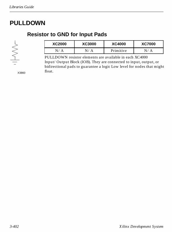
Libraries Guide
PULLDOWN
Resistor to GND for Input Pads
PULLDOWN resistor elements are available in each XC4000Input/Output Block (IOB). They are connected to input, output, orbidirectional pads to guarantee a logic Low level for nodes that mightfloat.
XC2000 XC3000 XC4000 XC7000
N/A N/A Primitive N/A
X3860
3-402 Xilinx Development System

Design Elements
PULLUP
Resistor to V CC for Input PADs, Open-Drain, and3-State Outputs
PULLUP resistor elements are available in each XC3000 and XC4000Input/Output Block (IOB). XC3000 IOBs only use PULLUP resistorson input pads. XC4000 IOBs connect PULLUP resistors to input,output, or bidirectional pads to guarantee a logic High level fornodes that might float.
The pull-up elements also establish a High logic level for open-drainelements and macros (DECODE, WAND, WORAND) or 3-statenodes (TBUF) when all the drivers are off.
The buffer outputs are connected together as a wired-AND to formthe output (O). When all the inputs are High, the output is off. Toestablish an output High level, a PULLUP resistor(s) is tied to output(O). One PULLUP resistor uses the least power, two pull-up resistorsachieve the fastest Low-to-High speed.
To indicate two PULLUP resistors, append a DOUBLE parameter tothe pull-up symbol attached to the output (O) node. Refer to theappropriate CAE tool interface user guide for details.
The PULLUP element is ignored in XC7000 designs. PULLUP is onlysupported for compatibility with FPGA designs. Internal 3-statenodes (from BUFE or BUFT) in EPLD designs are always pulled upwhen not driven.
XC2000 XC3000 XC4000 XC7000
N/A Primitive Primitive Primitive
X3861
Libraries Guide 3-403

Libraries Guide
RAM16X1
16-Deep by 1-Wide Static RAM
* Not supported for XC4010D designs
RAM16X1 is a 16-word by 1-bit static read-write random-accessmemory. When the write enable (WE) is High, the data on the datainput (D) is loaded into the word selected by the 4-bit address(A3 – A0). The data output (O) reflects the selected (addressed) word,whether WE is High or Low. When WE is Low, the RAM content isunaffected by address or input data transitions. Address inputs mustbe stable before the High-to-Low WE transition for predictableperformance.
RAM16X1 cannot be initialized during configuration, only afterconfiguration. Mode selection is shown in the following truth table.
data = word addressed by bits A3 – A0
XC2000 XC3000 XC4000 XC7000
N/A N/A Primitive* N/A
Inputs Outputs
WE(mode) D O
0(read) X data1(write) D data
X4124
RAM16X1
A3
A2
A1A0
WE
D O
3-404 Xilinx Development System

Design Elements
RAM16X2
16-Deep by 2-Wide Static RAM
* Not supported for XC4010D designs
RAM16X2 is a 16-word by 2-bit static read-write random-accessmemory. When the write enable (WE) is High, the data on data inputs(D1 – D0) is loaded into the word selected by the 4-bit address(A3 – A0). The data outputs (O1 – O0) reflect the selected (addressed)word, whether WE is High or Low. When WE is Low, the RAMcontent is unaffected by address or data input transitions. Addressinputs must be stable before the High-to-Low WE transition forpredictable performance.
RAM16X2 cannot be initialized during configuration, only afterconfiguration. Mode selection is shown in the following truth table.
data = word addressed by bits A3 – A0
XC2000 XC3000 XC4000 XC7000
N/A N/A Macro* N/A
Inputs Outputs
WE(mode) D1 – D0 O1 – O0
0(read) X data1(write) D1 – D0 data
X4128
RAM16X2 O0
A1
A2
A3
A0
WE
D1
D0
O1
Libraries Guide 3-405

Libraries Guide
RAM16X4
16-Deep by 4-Wide Static Ram
* Not supported for XC4010D designs
RAM16X4 is a 16-word by 4-bit static read-write random-accessmemory. When the write enable (WE) is High, the data on data inputs(D3 – D0) is loaded into the word selected by the 4-bit address(A3 – A0). The data outputs (O3 – O0) reflect the selected (addressed)word, whether WE is High or Low. When WE is Low, the RAMcontent is unaffected by address or data input transitions. Addressinputs must be stable before the High-to-Low WE transition forpredictable performance.
RAM16X4 cannot be initialized during configuration, only afterconfiguration. Mode selection is shown in the following truth table.
data = word addressed by bits A3 – A0
XC2000 XC3000 XC4000 XC7000
N/A N/A Macro* N/A
Inputs Outputs
WE(mode) D3 – D0 O3 – O0
0(read) X data1(write) D3 – D0 data
X4135
RAM16X4 O0
A1
A2
A3
A0
WE
D3
D2
O1
O2
O3
D1
D0
3-406 Xilinx Development System
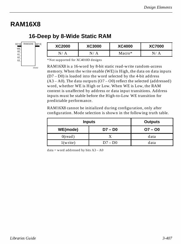
Design Elements
RAM16X8
16-Deep by 8-Wide Static RAM
* Not supported for XC4010D designs
RAM16X8 is a 16-word by 8-bit static read-write random-accessmemory. When the write enable (WE) is High, the data on data inputs(D7 – D0) is loaded into the word selected by the 4-bit address(A3 – A0). The data outputs (O7 – O0) reflect the selected (addressed)word, whether WE is High or Low. When WE is Low, the RAMcontent is unaffected by address or data input transitions. Addressinputs must be stable before the High-to-Low WE transition forpredictable performance.
RAM16X8 cannot be initialized during configuration, only afterconfiguration. Mode selection is shown in the following truth table.
data = word addressed by bits A3 – A0
XC2000 XC3000 XC4000 XC7000
N/A N/A Macro* N/A
Inputs Outputs
WE(mode) D7 – D0 O7 – O0
0(read) X data1(write) D7 – D0 data
X4142
RAM16X8
A0 WE
D[7:0] Q[7:0]
A1A2A3
Libraries Guide 3-407

Libraries Guide
Figure 3-186 RAM16X8 XC4000 Implementation
O0
A0A1A2A3
D OWE
RAM16X1
O7
O6
O0
O5
O4
O1
O2
O3
O[7:0]
A2
D[7:0]
D4
D5
D6
D7
D0
D1
D2
D3
A3
A1A0WE
O1
A0A1A2A3
D OWE
RAM16X1
O2
A0A1A2A3
D OWE
RAM16X1
O3
A0A1A2A3
D OWE
RAM16X1
O4
A0A1A2A3
D OWE
RAM16X1
O5
A0A1A2A3
D OWE
RAM16X1
O6
A0A1A2A3
D OWE
RAM16X1
O7
A0A1A2A3
D OWE
RAM16X1
3-408 Xilinx Development System
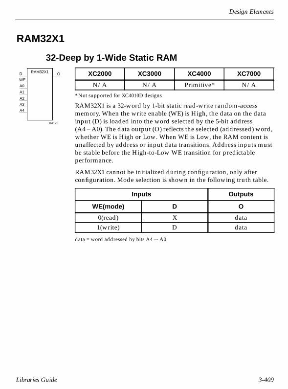
Design Elements
RAM32X1
32-Deep by 1-Wide Static RAM
* Not supported for XC4010D designs
RAM32X1 is a 32-word by 1-bit static read-write random-accessmemory. When the write enable (WE) is High, the data on the datainput (D) is loaded into the word selected by the 5-bit address(A4 – A0). The data output (O) reflects the selected (addressed) word,whether WE is High or Low. When WE is Low, the RAM content isunaffected by address or input data transitions. Address inputs mustbe stable before the High-to-Low WE transition for predictableperformance.
RAM32X1 cannot be initialized during configuration, only afterconfiguration. Mode selection is shown in the following truth table.
data = word addressed by bits A4 –- A0
XC2000 XC3000 XC4000 XC7000
N/A N/A Primitive* N/A
Inputs Outputs
WE(mode) D O
0(read) X data1(write) D data
X4125
RAM32X1 O
A2
A3
A4
A1
A0
WE
D
Libraries Guide 3-409

Libraries Guide
RAM32X2
32-Deep by 2-Wide Static RAM
* Not supported for XC4010D designs
RAM32X2 is a 32-word by 2-bit static read-write random-accessmemory. When the write enable (WE) is High, the data on the datainputs (D1 – D0) is loaded into the word selected by the address bits(A4 – A0). The data outputs (O1 – O0) reflect the selected (addressed)word, whether WE is High or Low. When WE is Low, the RAMcontent is unaffected by address or input data transitions. Addressinputs must be stable before the High-to- Low WE transition forpredictable performance.
RAM32X2 cannot be initialized during configuration, only afterconfiguration. Mode selection is shown in the following truth table.
data = word addressed by bits A4 –- A0
XC2000 XC3000 XC4000 XC7000
N/A N/A Macro* N/A
Inputs Outputs
WE(mode) D1 – D0 O1 – O0
0(read) X data1(write) D1 – D0 data
X4129
RAM32X2
O0
A2
A3
A4
A1
A0
WE
D1
D0 O1
3-410 Xilinx Development System

Design Elements
RAM32X4
32-Deep by 4-Wide Static RAM
* Not supported for XC4010D designs
RAM32X4 is a 32-word by 4-bit static read-write random-accessmemory. When the write enable (WE) is High, the data on the datainputs (D3 – D0) is loaded into the word selected by the address bits(A4 – A0). The data outputs (O3 – O0) reflect the selected (addressed)word, whether WE is High or Low. When WE is Low, the RAMcontent is unaffected by address or input data transitions. Addressinputs must be stable before the High-to- Low WE transition forpredictable performance.
RAM32X4 cannot be initialized during configuration, only afterconfiguration. Mode selection is shown in the following truth table.
data = word addressed by bits A4 –- A0
XC2000 XC3000 XC4000 XC7000
N/A N/A Macro* N/A
Inputs Outputs
WE(mode) D3 – D0 O3 – O0
0(read) X data1(write) D3 – D0 data
X4136
RAM32X4 O0
A1
A2
A3
A0
WE
D3
D2
O1
O2
O3
D1
D0
A4
Libraries Guide 3-411

Libraries Guide
RAM32X8
32-Deep by 8-Wide Static RAM
* Not supported for XC4010D designs
RAM32X8 is a 32-word by 8-bit static read-write random-accessmemory. When the write enable (WE) is High, the data on the datainputs (D7 – D0) is loaded into the word selected by the address bits(A4 – A0). The data outputs (O7 – O0) reflect the selected (addressed)word, whether WE is High or Low. When WE is Low, the RAMcontent is unaffected by address or input data transitions. Theaddress inputs must be stable before the High-to- Low WE transitionfor predictable performance.
RAM32X8 cannot be initialized during configuration, only afterconfiguration. Mode selection is shown in the following truth table.
data = word addressed by bits A4 –- A0
XC2000 XC3000 XC4000 XC7000
N/A N/A Macro* N/A
Inputs Outputs
WE(mode) D7 – D0 O7 – O0
0(read) X data1(write) D7 – D0 data
X4143
RAM32X8
A0 WE
D[7-0] Q[7-0]
A1A2A3
A4
3-412 Xilinx Development System

Design Elements
Figure 3-187 RAM32X8 XC4000 Implementation
O7A4
O
A2A1
RAM32X1DWEA0
A3
WEA0
O7
O6
O0
O5
O4
O1
O2
O3
O[7:0]
D7
D[7:0]
D4
D5
D6
D0
D1
D2
D3
A3A2A1
A4
O0A4
O
A2A1
RAM32X1DWEA0
A3
O1A4
O
A2A1
RAM32X1DWEA0
A3
O2A4
O
A2A1
RAM32X1DWEA0
A3
O3A4
O
A2A1
RAM32X1DWEA0
A3
O4A4
O
A2A1
RAM32X1DWEA0
A3
O5A4
O
A2A1
RAM32X1DWEA0
A3
O6A4
O
A2A1
RAM32X1DWEA0
A3
Libraries Guide 3-413

Libraries Guide
READBACK
FPGA Bitstream Readback Controller
The READBACK macro accesses the bitstream readback function. ALow-to-High transition on the TRIG input initiates the readbackprocess. The readback data appears on the DATA output. The RIP(readback-in-progress) output remains High during the readbackprocess. If you use the ReadAbort:Enable option in MakeBits, a High-to-Low transition on the TRIG input aborts the process. The signal onthe CLK input clocks out the readback data; if no signal is connectedto the CLK input, the internal CCLK is used. Set the ReadClk optionin MakeBits to indicate the readback clock source.
Typically, READBACK inputs are sourced by device-external inputpins and outputs drive device-external output pins. If you wantexternal input and output pins, connect READBACK pins throughIBUFs or OBUFs to pads, as with any I/O device. However, you canconnect READBACK pins to device-internal logic instead. For detailson the readback process, refer to the application note “Using theXC4000 Readback Capability” in The Programmable Logic Data Book.
Figure 3-188 READBACK XC4000 Implementation
XC2000 XC3000 XC4000 XC7000
N/A N/A Macro N/AX3918
RIP
READBACKCLK
TRIG
DATA
DATARIP
TRIG
RDBK
I
RDCLKCLK
TRIG DATARIP
3-414 Xilinx Development System
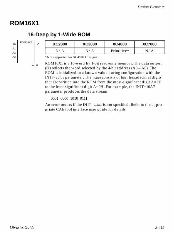
Design Elements
ROM16X1
16-Deep by 1-Wide ROM
* Not supported for XC4010D designs
ROM16X1 is a 16-word by 1-bit read-only memory. The data output(O) reflects the word selected by the 4-bit address (A3 – A0). TheROM is initialized to a known value during configuration with theINIT=value parameter. The value consists of four hexadecimal digitsthat are written into the ROM from the most-significant digit A=FHto the least-significant digit A=0H. For example, the INIT=10A7parameter produces the data stream
0001 0000 1010 0111
An error occurs if the INIT=value is not specified. Refer to the appro-priate CAE tool interface user guide for details.
XC2000 XC3000 XC4000 XC7000
N/A N/A Primitive* N/A
X4137
ROM16X1A0
A1
A2
A3
O
Libraries Guide 3-415

Libraries Guide
ROM32X1
32-Deep by 1-Wide ROM
* Not supported for XC4010D designs
ROM32X1 is a 32-word by 1-bit read-only memory. The data output(O) reflects the word selected by the 5-bit address (A4 – A0). TheROM is initialized to a known value during configuration with theINIT=value parameter. The value consists of eight hexadecimal digitsthat are written into the ROM from the most-significant digit A=1FHto the least-significant digit A=00H. For example, the INIT=10A78F39parameter produces the data stream
0001 0000 1010 0111 1000 1111 0011 1001
An error occurs if the INIT=value is not specified. Refer to the appro-priate CAE tool interface user guide for details.
XC2000 XC3000 XC4000 XC7000
N/A N/A Primitive* N/A
X4130
ROM32X1O
A2
A3
A4
A1
A0
3-416 Xilinx Development System

Design Elements
SOP
Sum Of Products
Sum Of Products macros and primitives provide common logic func-tions by OR gating the outputs of two AND functions or the outputof one AND function with one direct input. Variations of invertingand non-inverting inputs are available.
Figure 3-189 SOP Gate Representations
Name XC2000 XC3000 XC4000 XC7000
SOP3 – SOP3B3 Macro Macro Macro PrimitiveSOP4 – SOP4B4 Macro Macro Macro Primitive
SOP3B3
SOP3B2B
SOP3B2A
SOP3B1B
SOP3B1A
SOP3SOP4
SOP4B1
SOP4B2A
SOP4B2B
SOP4B3
SOP4B4
Libraries Guide 3-417

Libraries Guide
SR4CE
4-Bit Serial-In Parallel-Out Shift Register with ClockEnable and Asynchronous Clear
SR4CE is a 4-bit shift register with a shift-left serial input (SLI),parallel outputs (Q3 – Q0), and clock enable (CE) and asynchronousclear (CLR) inputs. The CLR input, when High, overrides all otherinputs and resets the data outputs (Q3 – Q0) Low. When CE is Highand CLR is Low, the data on the SLI input is loaded into the first bit ofthe shift register during the Low-to-High clock (C) transition andappears on the Q0 output. During subsequent Low-to-High clocktransitions, when CE is High and CLR is Low, data is shifted to thenext highest bit position as new data is loaded into Q0 (SLI➝Q0,Q0➝Q1, Q1➝Q2, and so forth). The register ignores clock transitionswhen CE is Low.
Registers can be cascaded by connecting the Q3 output of one stage tothe SLI input of the next stage and connecting clock, CE, and CLR inparallel.
The register is asynchronously reset, outputs Low, when power isapplied or when Global Reset (XC2000, XC3000) or Global Set/Reset(XC4000) is active. GR is active-Low; the GSR active level is program-mable.
qn-1 = state of referenced output one set-up time prior to active clock transition
XC2000 XC3000 XC4000 XC7000
Macro Macro Macro Primitive
Inputs Outputs
CLR CE SLI C Q0 Q3 – Q1
1 X X X 0 00 0 X X ---No Change---0 1 1 ↑ 1 qn-10 1 0 ↑ 0 qn-1
X4145
SR4CE
C
CE
SLI
Q3
Q2
Q1
Q0
CLR
3-418 Xilinx Development System

Design Elements
SR4CLE
4-Bit Loadable Serial/Parallel-In Parallel-Out ShiftRegister with Clock Enable and Asynchronous Clear
SR4CLE is a 4-bit shift register with a shift-left serial input (SLI),parallel inputs (D3 – D0), parallel outputs (Q3 – Q0), and threecontrol inputs – clock enable (CE), load enable (L), and asynchronousclear (CLR).The register ignores clock transitions when L and CE areLow. The asynchronous CLR, when High, overrides all other inputsand resets the data outputs (Q3 – Q0) Low. When L is High and CLRis Low, data on the D3 – D0 inputs is loaded into the correspondingQ3 – Q0 bits of the register. When CE is High and L and CLR are Low,data on the SLI input is loaded into the first bit of the shift registerduring the Low-to-High clock (C) transition and appears on the Q0output. During subsequent clock transitions, when CE is High and Land CLR are Low, the data is shifted to the next highest bit position asnew data is loaded into Q0 (SLI➝Q0, Q0➝Q1, Q1➝Q2, and so forth).
Registers can be cascaded by connecting the Q3 output of one stageto the SLI input of the next stage and connecting clock, CE, L, andCLR inputs in parallel.
The register is asynchronously reset, outputs Low, when power isapplied or when Global Reset (XC2000, XC3000) or Global Set/Reset(XC4000) is active. GR is active-Low; the GSR active level is program-mable.
dn or qn-1 = state of referenced input or output one set-up time prior to activeclock transition
XC2000 XC3000 XC4000 XC7000
Macro Macro Macro Primitive
Inputs Outputs
CLR L CE SLI D3 – D0 C Q0 Q3 – Q1
1 X X X X X 0 00 1 X X D3 – D0 ↑ d0 dn0 0 1 SLI X ↑ SLI qn-10 0 0 X X X --No Change--
X4147
C
CE
L
SR4CLE
D3
D2
D1
D0
SLI
Q3
Q2
Q1
Q0
CLR
Libraries Guide 3-419

Libraries Guide
SR4CLED
4-Bit Shift Register with Clock Enable andAsynchronous Clear
SR4CLED is a 4-bit shift register with shift-left (SLI) and shift-right(SRI) serial inputs, four parallel inputs (D3 – D0), and four controlinputs – clock enable (CE), load enable (L), shift left/right (LEFT),and asynchronous clear (CLR). The register ignores clock transitionswhen CE and L are Low. The asynchronous clear, when High, over-rides all other inputs and resets the data outputs (Q3 – Q0) Low.When L is High and CLR is Low, the data on the D3 – D0 inputs isloaded into the corresponding Q3 – Q0 bits of the register. When CEis High and L and CLR are Low, data is shifted right or left,depending on the state of the LEFT input. If LEFT is High, data on theSLI is loaded into Q0 during the Low-to-High clock transition andshifted left (to Q1, Q2, and so forth) during subsequent clock transi-tions. If LEFT is Low, data on the SRI is loaded into Q3 during theLow-to-High clock transition and shifted right (to Q2, Q1, and soforth) during subsequent clock transitions. The truth table indicatesthe state of the Q3 – Q0 outputs under all input conditions.
The register is asynchronously reset, outputs Low, when power isapplied, or when Global Reset (XC2000, XC3000) or Global Set/Reset(XC4000) is active. GR is active-Low; the GSR active level is program-mable.
dn, qn-1 or qn+1 = state of referenced input one set-up time prior to active clocktransition
XC2000 XC3000 XC4000 XC7000
Macro Macro Macro Primitive
Inputs Outputs
CLR L CE LEFT SLI SRI D3 – D0 C Q0 Q3 Q2 – Q1
1 X X X X X X X 0 0 00 1 X X X X D3 – D0 ↑ d0 d3 dn0 0 0 X X X X X ----No Change-----0 0 1 1 SLI X X ↑ SLI q2 qn-10 0 1 0 X SRI X ↑ q1 SRI qn+1
X4149
C
CE
L
SR4CLED
D3
D2
D1
D0
SLI
Q3
Q2
Q1
Q0
CLR
SRI
LEFT
3-420 Xilinx Development System

Design Elements
SR4RE
4-Bit Serial-In Parallel-Out Shift Register with ClockEnable and Synchronous Reset
SR4RE is a 4-bit shift register with shift-left serial input (SLI), paralleloutputs (Q3 – Q0), clock enable (CE), and synchronous reset (R)inputs. The R input, when High, overrides all other inputs and resetsthe data outputs (Q3 – Q0) Low. When CE is High and R is Low, thedata on the SLI is loaded into the first bit of the shift register duringthe Low-to-High clock (C) transition and appears on the Q0 output.During subsequent Low-to-High clock transitions, when CE is Highand R is Low, data is shifted to the next highest bit position as newdata is loaded into Q0 (SLI➝Q0, Q0➝Q1, Q1➝Q2, and so forth). Theregister ignores clock transitions when CE is Low.
Registers can be cascaded by connecting the Q3 output of one stageto the SLI input of the next stage and connecting clock, CE, and R inparallel.
The register is asynchronously reset, outputs Low, when power isapplied or when Global Reset (XC2000, XC3000) or Global Set/Reset(XC4000) is active. GR is active-Low; the GSR active level is program-mable.
qn-1 = state of referenced output one set-up time prior to active clock transition
XC2000 XC3000 XC4000 XC7000
Macro Macro Macro Primitive
Inputs Outputs
R CE SLI C Q0 Q3 – Q1
1 X X ↑ 0 00 0 X X ---No Change---0 1 1 ↑ 1 qn-10 1 0 ↑ 0 qn-1
X4144
SR4RE
C
CE
SLI
Q3
Q2
Q1
Q0
R
Libraries Guide 3-421

Libraries Guide
SR4RLE
4-Bit Loadable Serial/Parallel-In Parallel-Out ShiftRegister with Clock Enable and Synchronous Reset
SR4RLE is a 4-bit shift register with shift-left serial input (SLI),four parallel inputs (D3 – D0), four parallel outputs (Q3 – Q0), andthree control inputs – clock enable (CE), load enable (L), and synchro-nous reset (R). The register ignores clock transitions when L and CEare Low. The synchronous R, when High, overrides all other inputsand resets the data outputs (Q3 – Q0) Low. When L is High and R isLow, data on the D3 – D0 inputs is loaded into the correspondingQ3 – Q0 bits of the register. When CE is High and L and R are Low,data on the SLI input is loaded into the first bit of the shift registerduring the Low-to-High clock (C) transition and appears on the Q0output. During subsequent clock transitions, when CE is High and Land R are Low, the data is shifted to the next highest bit position asnew data is loaded into Q0 (SLI➝Q0, Q0➝Q1, Q1➝Q2, and so forth).
Registers can be cascaded by connecting the Q3 output of one stage tothe SLI input of the next stage and connecting clock, CE, L, and Rinputs in parallel.
The register is asynchronously reset, outputs Low, when power isapplied or when Global Reset (XC2000, XC3000) or Global Set/Reset(XC4000) is active. GR is active-Low; the GSR active level is program-mable.
dn or qn-1 = state of referenced input one set-up time prior to active clocktransition
XC2000 XC3000 XC4000 XC7000
Macro Macro Macro Primitive
Inputs Outputs
R L CE SLI D3 – D0 C Q0 Q3 – Q1
1 X X X X ↑ 0 00 1 X X D3 – D0 ↑ d0 dn0 0 1 SLI X ↑ SLI qn-10 0 0 X X X --No Change--
X4146
C
CE
L
SR4RLE
D3
D2
D1
D0
SLI
Q3
Q2
Q1
Q0
R
3-422 Xilinx Development System

Design Elements
SR4RLED
4-Bit Shift Register with Clock Enable andSynchronous Reset
SR4RLED is a 4-bit shift register with shift-left (SLI) and shift-right(SRI) serial inputs, four parallel inputs (D3 – D0), and four controlinputs – clock enable (CE), load enable (L), shift left/right (LEFT),and synchronous reset (R). The register ignores clock transitionswhen CE and L are Low. The synchronous R, when High, overridesall other inputs and resets the data outputs (Q3 – Q0) Low. When L isHigh and R is Low, the data on the D3 – D0 inputs is loaded into thecorresponding Q3 – Q0 bits of the register. When CE is High and Land R are Low, data is shifted right or left, depending on the state ofthe LEFT input. If LEFT is High, data on SLI is loaded into Q0 duringthe Low-to-High clock transition and shifted left (to Q1, Q2, and soforth) during subsequent clock transitions. If LEFT is Low, data onthe SRI is loaded into Q3 during the Low-to-High clock transitionand shifted right (to Q2, Q1, and so forth) during subsequent clocktransitions. The truth table indicates the state of the Q3 – Q0 outputsunder all input conditions.
The register is asynchronously reset, outputs Low, when power isapplied or when Global Reset (XC2000, XC3000) or Global Set/Reset(XC4000) is active. GR is active-Low; the GSR active level is program-mable.
dn, qn-1 or qn+1 = state of referenced input one set-up time prior to active clocktransition
XC2000 XC3000 XC4000 XC7000
Macro Macro Macro Primitive
Inputs Outputs
R L CE LEFT SLI SRI D3 – D0 C Q0 Q3 Q2 – Q1
1 X X X X X X ↑ 0 0 00 1 X X X X D3 – D0 ↑ d0 d3 dn0 0 0 X X X X X ----No Change-----0 0 1 1 SLI X X ↑ SLI q2 qn-10 0 1 0 X SRI X ↑ q1 SRI qn+1
X4148
C
CE
L
SR4RLED
D3
D2
D1
D0
SLI
Q3
Q2
Q1
Q0
R
SRI
LEFT
Libraries Guide 3-423

Libraries Guide
SR8CE
8-Bit Serial-In Parallel-Out Shift Register with ClockEnable and Asynchronous Clear
SR8CE is an 8-bit shift-left serial input (SLI), parallel output (Q7 – Q0)shift register with clock enable (CE) and asynchronous clear (CLR)inputs. The CLR input, when High, overrides all other inputs andresets the data outputs (Q7 – Q0) Low. When CE is High and CLR isLow, the data on the SLI is loaded into the first bit of the shift registerduring the Low-to-High clock (C) transition and appears on the Q0output. During subsequent Low-to-High clock transitions, when CEis High and CLR is Low, data is shifted to the next highest bit positionas new data is loaded into Q0 (SLI➝Q0, Q0➝Q1, Q1➝Q2, and soforth). The register ignores clock transitions when CE is Low.
Registers can be cascaded by connecting the Q7 output of one stage tothe SLI input of the next stage and connecting clock, CE, and CLR inparallel.
The register is asynchronously reset, outputs Low, when power isapplied or when Global Reset (XC2000, XC3000) or Global Set/Reset(XC4000) is active. GR is active-Low; the GSR active level is program-mable.
qn-1 = state of referenced output one set-up time prior to active clock transition
XC2000 XC3000 XC4000 XC7000
Macro Macro Macro Primitive
Inputs Outputs
CLR CE SLI C Q0 Q7 – Q1
1 X X X 0 00 0 X X --No Change---0 1 1 ↑ 1 qn-10 1 0 ↑ 0 qn-1
X4151
SR8CE
C
CE
SLIQ[7:0]
CLR
3-424 Xilinx Development System

Design Elements
Figure 3-190 SR8CE XC2000/3000/4000 Implementation
Q6
FDCEQD
CLR
CEC
Q2
FDCEQD
CLR
CEC
Q0
FDCEQD
CLR
CEC
Q1
FDCEQD
CLR
CEC
Q4
FDCEQD
CLR
CEC
Q5
FDCEQD
CLR
CEC
Q3
FDCEQD
CLR
CEC
Q7
FDCEQD
CLR
CEC
SLICE
CCLR
Q6
Q1
Q2
Q3
Q0 Q3
Q[7:0]
Q4
Q5
Q7
C
Libraries Guide 3-425
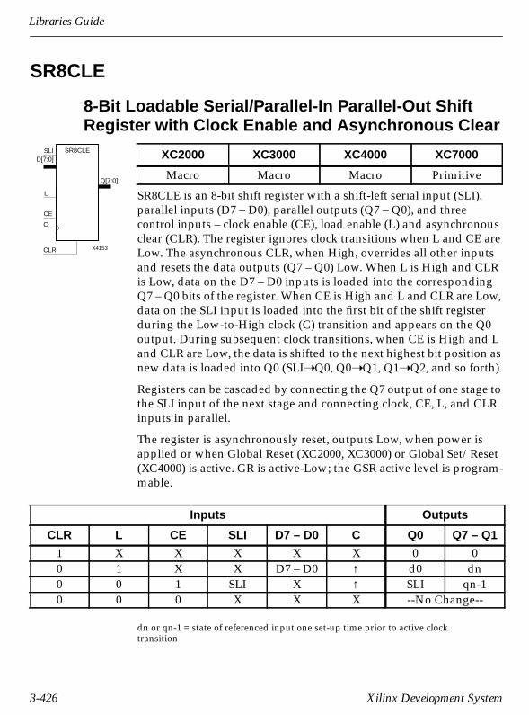
Libraries Guide
SR8CLE
8-Bit Loadable Serial/Parallel-In Parallel-Out ShiftRegister with Clock Enable and Asynchronous Clear
SR8CLE is an 8-bit shift register with a shift-left serial input (SLI),parallel inputs (D7 – D0), parallel outputs (Q7 – Q0), and threecontrol inputs – clock enable (CE), load enable (L) and asynchronousclear (CLR). The register ignores clock transitions when L and CE areLow. The asynchronous CLR, when High, overrides all other inputsand resets the data outputs (Q7 – Q0) Low. When L is High and CLRis Low, data on the D7 – D0 inputs is loaded into the correspondingQ7 – Q0 bits of the register. When CE is High and L and CLR are Low,data on the SLI input is loaded into the first bit of the shift registerduring the Low-to-High clock (C) transition and appears on the Q0output. During subsequent clock transitions, when CE is High and Land CLR are Low, the data is shifted to the next highest bit position asnew data is loaded into Q0 (SLI➝Q0, Q0➝Q1, Q1➝Q2, and so forth).
Registers can be cascaded by connecting the Q7 output of one stage tothe SLI input of the next stage and connecting clock, CE, L, and CLRinputs in parallel.
The register is asynchronously reset, outputs Low, when power isapplied or when Global Reset (XC2000, XC3000) or Global Set/Reset(XC4000) is active. GR is active-Low; the GSR active level is program-mable.
dn or qn-1 = state of referenced input one set-up time prior to active clocktransition
XC2000 XC3000 XC4000 XC7000
Macro Macro Macro Primitive
Inputs Outputs
CLR L CE SLI D7 – D0 C Q0 Q7 – Q1
1 X X X X X 0 00 1 X X D7 – D0 ↑ d0 dn0 0 1 SLI X ↑ SLI qn-10 0 0 X X X --No Change--
X4153
C
CE
L
SR8CLED[7:0]
SLI
Q[7:0]
CLR
3-426 Xilinx Development System

Design Elements
Figure 3-191 SR8CLE XC2000/3000/4000 Implementation
Q[7:0]
Q3
Q0
Q1
Q2
Q4
Q5
Q6
Q7
Q3
D[7:0]
D3
D2
D0
D1
D4
D5
D6
D7
MQ4
D0D1
O
S0
M2_1
MD5
CLR
L_OR_CE
MD7
C
MQ3
D0D1
O
S0
M2_1
L
SLI
MD2 MD6
MD4
MD3
MD1
MD0
Q1
FDCEQD
CLRCEC
Q2
FDCEQD
CLRCEC
Q3
FDCEQD
CLRCEC
Q4
FDCEQD
CLRCEC
Q6
FDCEQD
CLRCEC
Q7
FDCEQD
CLRCEC
MQ0
D0D1
O
S0
M2_1
MQ1
D0D1
O
S0
M2_1
MQ2
D0D1
O
S0
M2_1
MQ5
D0D1
O
S0
M2_1
MQ7
D0D1
O
S0
M2_1
MQ6
D0D1
O
S0
M2_1
OR2
CE
Q0
FDCEQD
CLRCEC
Q5
FDCEQD
CLRCEC
Libraries Guide 3-427

Libraries Guide
SR8CLED
8-Bit Shift Register with Clock Enable andAsynchronous Clear
SR8CLED is an 8-bit shift register with shift-left (SLI) and shift-right(SRI) serial inputs, parallel inputs (D7 – D0), and four control inputs –clock enable (CE), load enable (L), shift left/right (LEFT), and asyn-chronous clear (CLR). The register ignores clock transitions when CEand L are Low. The asynchronous CLR, when High, overrides allother inputs and resets the data outputs (Q7 – Q0) Low. When L isHigh and CLR is Low, data on the D7 – D0 inputs is loaded into thecorresponding Q7 – Q0 bits of the register. When CE is High and Land CLR are Low, data is shifted right or left depending on the stateof the LEFT input. If LEFT is High, data on the SLI is loaded into Q0during the Low-to-High clock transition and shifted left (to Q1, Q2,and so forth) during subsequent clock transitions. If LEFT is Low,data on the SRI is loaded into Q7 during the Low-to-High clock tran-sition and shifted right (to Q6, Q5, and so forth) during subsequentclock transitions. The truth table indicates the state of the Q7 – Q0outputs under all input conditions.
The register is asynchronously reset, outputs Low, when power isapplied or when Global Reset (XC2000, XC3000) or Global Set/Reset(XC4000) is active. GR is active-Low; the GSR active level is program-mable.
dn, qn-1 or qn+1 = state of referenced input one set-up time prior to active clocktransition
XC2000 XC3000 XC4000 XC7000
Macro Macro Macro Primitive
Inputs Outputs
CLR L CE LEFT SLI SRI D7 – D0 C Q0 Q7 Q6 – Q1
1 X X X X X X X 0 0 00 1 X X X X D7 – D0 ↑ d0 d7 dn0 0 0 X X X X X -----No Change-----0 0 1 1 SLI X X ↑ SLI q6 qn-10 0 1 0 X SRI X ↑ q1 SRI qn+1
X4155
C
CE
L
SR8CLEDD[7:0]
SLI
Q[7:0]
CLR
SRI
LEFT
3-428 Xilinx Development System

Design Elements
Figure 3-192 SR8CLED XC2000/3000/4000 Implementation
LEFT
OR2
L
MDR7
MDR6
MDR5
MDR4
MDR3
MDR2
MDR1
MDR0
MDL7
MDL5
MDL4
MDL3
MDL2
MDL1
MDL0
D4
D2
D1
D0
D3
D5
D6
D7D[7:0]
SLI
CE
Q0
Q1
Q2
Q3
Q4
Q5
Q6
Q7
Q[7:0]
MDL6
L_OR_CE
Q0
FDCEQD
CLR
CEC
Q1
FDCEQD
CLR
CEC
Q2
FDCEQD
CLR
CEC
Q3
FDCEQD
CLR
CEC
Q4
FDCEQD
CLRCEC
Q5
FDCEQD
CLR
CEC
Q6
FDCEQD
CLR
CEC
Q7
FDCEQD
CLRCEC
MDR4
D0D1
O
S0
M2_1
MDL6
D0D1
O
S0
M2_1
MDL5
D0D1
O
S0
M2_1
MDL4
D0D1
O
S0
M2_1
MDR5
D0D1
O
S0
M2_1
MDR6
D0D1
O
S0
M2_1
MDL7
D0D1
O
S0
M2_1
MDR7
D0D1
O
S0
M2_1
MDR3
D0D1
O
S0
M2_1
MDL3
D0D1
O
S0
M2_1
MDR2
D0D1
O
S0
M2_1
MDR1
D0D1 O
S0
M2_1
MDR0
D0D1
O
S0
M2_1OR2
MDL0
D0D1
O
S0
M2_1
MDL1
D0D1 O
S0
M2_1
MDL2
D0D1
O
S0
M2_1
SRIL_LEFT
CLRC
Libraries Guide 3-429

Libraries Guide
SR8RE
8-Bit Serial-In Parallel-Out Shift Register with ClockEnable and Synchronous Reset
SR8RE is an 8-bit shift-left serial input (SLI), parallel output (Q7 – Q0)shift register with clock enable (CE) and synchronous reset (R) inputs.The R input, when High, overrides all other inputs and resets the dataoutputs (Q7 – Q0) Low. When CE is High and R is Low, the data onthe SLI is loaded into the first bit of the shift register during the Low-to-High clock (C) transition and appears on the Q0 output. Duringsubsequent Low-to-High clock transitions, when CE is High and R isLow, data is shifted to the next highest bit position as new data isloaded into Q0 (SLI➝Q0, Q0➝Q1, Q1➝Q2, and so forth). The registerignores clock transitions when CE is Low.
Registers can be cascaded by connecting the Q7 output of one stage tothe SLI input of the next stage and by connecting clock, CE, and R inparallel.
The register is asynchronously reset, outputs Low, when power isapplied or when Global Reset (XC2000, XC3000) or Global Set/Reset(XC4000) is active. GR is active-Low; the GSR active level is program-mable.
qn-1 = state of referenced output one set-up time prior to active clock transition
XC2000 XC3000 XC4000 XC7000
Macro Macro Macro Primitive
Inputs Outputs
R CE SLI C Q0 Q7 – Q1
1 X X ↑ 0 00 0 X X --No Change---0 1 1 ↑ 1 qn-10 1 0 ↑ 0 qn-1
X4150
SR8RE
C
CE
SLIQ[7:0]
R
3-430 Xilinx Development System

Design Elements
Figure 3-193 SR8RE XC2000/3000/4000 Implementation
Q7
FDRE
R
QDCEC
Q6
FDRE
R
QDCEC
Q5
FDRE
R
QDCEC
Q4
FDRE
R
QDCEC
Q3
FDRE
R
QDCEC
Q2
FDRE
R
QDCEC
Q1
FDRE
R
QDCEC
Q0
FDRE
R
QDCEC
SLICE
R
Q6
Q1
Q2
Q3
Q0 Q3
Q[7:0]
Q4
Q5
Q7
C
Libraries Guide 3-431
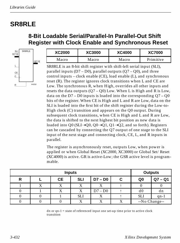
Libraries Guide
SR8RLE
8-Bit Loadable Serial/Parallel-In Parallel-Out ShiftRegister with Clock Enable and Synchronous Reset
SR8RLE is an 8-bit shift register with shift-left serial input (SLI),parallel inputs (D7 – D0), parallel outputs (Q7 – Q0), and threecontrol inputs – clock enable (CE), load enable (L), and synchronousreset (R). The register ignores clock transitions when L and CE areLow. The synchronous R, when High, overrides all other inputs andresets the data outputs (Q7 – Q0) Low. When L is High and R is Low,data on the D7 – D0 inputs is loaded into the corresponding Q7 – Q0bits of the register. When CE is High and L and R are Low, data on theSLI is loaded into the first bit of the shift register during the Low-to-High clock (C) transition and appears on the Q0 output. Duringsubsequent clock transitions, when CE is High and L and R are Low,the data is shifted to the next highest bit position as new data isloaded into Q0 (SLI➝Q0, Q0➝Q1, Q1➝Q2, and so forth). Registerscan be cascaded by connecting the Q7 output of one stage to the SLIinput of the next stage and connecting clock, CE, L, and R inputs inparallel.
The register is asynchronously reset, outputs Low, when power isapplied or when Global Reset (XC2000, XC3000) or Global Set/Reset(XC4000) is active. GR is active-Low; the GSR active level is program-mable.
dn or qn-1 = state of referenced input one set-up time prior to active clocktransition
XC2000 XC3000 XC4000 XC7000
Macro Macro Macro Primitive
Inputs Outputs
R L CE SLI D7 – D0 C Q0 Q7 – Q1
1 X X X X ↑ 0 00 1 X X D7 – D0 ↑ d0 dn0 0 1 SLI X ↑ SLI qn-10 0 0 X X X --No Change--
X4152
C
CE
L
SR8RLED[7:0]
SLI
Q[7:0]
R
3-432 Xilinx Development System

Design Elements
Figure 3-194 SR8RLE XC2000/3000/4000 Implementation
Q[7:0]
Q3
Q0
Q1
Q2
Q4
Q5
Q6
Q7
Q3
D[7:0]
D0
D1
D4
D5
D6
D7D3
D2
R
L
MD2
MD7
MD6
MD5
MD4
MD3
MD1
MD0
C
SLI
MQ0
D0D1 OS0
M2_1
MQ1
D0D1 OS0
M2_1
MQ2
D0D1 OS0
M2_1
MQ3
D0D1 OS0
M2_1
MQ4
D0D1 OS0
M2_1
MQ5
D0D1 OS0
M2_1
MQ7
D0D1 OS0
M2_1
MQ6
D0D1 OS0
M2_1
OR2
CE L_OR_CE
Q7
FDRE
R
QDCEC
Q6
FDRE
R
QDCEC
Q5
FDRE
R
QDCEC
Q4
FDRE
R
QDCEC
Q3
FDRE
R
QDCEC
Q2
FDRE
R
QDCEC
Q1
FDRE
R
QDCEC
Q0
FDRE
R
QDCEC
Libraries Guide 3-433

Libraries Guide
SR8RLED
8-Bit Shift Register with Clock Enable andSynchronous Reset
SR8RLED is an 8-bit shift register with shift-left (SLI) and shift-right(SRI) serial inputs, parallel inputs (D7 – D0), and four control inputs –clock enable (CE), load enable (L), shift left/right (LEFT), andsynchronous reset (R). The register ignores clock transitions when CEand L are Low. The synchronous R, when High, overrides all otherinputs and resets the data outputs (Q7 – Q0) Low. When L is Highand R is Low, the data on the D7 – D0 inputs is loaded into the corre-sponding Q7 – Q0 bits of the register. When CE is High and L and Rare Low, data is shifted right or left depending on the state of theLEFT input. If LEFT is High, data on SLI is loaded into Q0 during theLow-to-High clock transition and shifted left (to Q1, Q2, and so forth)during subsequent clock transitions. If LEFT is Low, data on SRI isloaded into Q7 bit during the Low-to-High clock transition andshifted right (to Q6, Q5, and so forth) during subsequent clock transi-tions. The truth table indicates the state of the Q7 – Q0 outputs underall input conditions.
The register is asynchronously reset, outputs Low, when power isapplied or when Global Reset (XC2000, XC3000) or Global Set/Reset(XC4000) is active. GR is active-Low; the GSR active level is program-mable.
dn, qn-1 or qn+1 = state of referenced input one set-up time prior to active clocktransition
XC2000 XC3000 XC4000 XC7000
Macro Macro Macro Primitive
Inputs Outputs
R L CE LEFT SLI SRI D7– D0 C Q0 Q7 Q6 – Q1
1 X X X X X X ↑ 0 0 00 1 X X X X D7 – D0 ↑ d0 d7 dn0 0 0 X X X X X ----No Change-----0 0 1 1 SLI X X ↑ SLI q6 qn-10 0 1 0 X SRI X ↑ q1 SRI qn+1
X4154
C
CE
L
SR8RLEDD[7:0]
SLI
Q[7:0]
R
SRI
LEFT
3-434 Xilinx Development System

Design Elements
Figure 3-195 SR8RLED XC2000/3000/4000 Implementation
LEFTOR2
L MDR7
D0D1
O
S0
M2_1
MDL5
D0D1
O
S0
M2_1
MDL1
D0D1
O
S0
M2_1
MDL0
D0D1
O
S0
M2_1
MDR7
MDR6
MDR5
MDR4
MDR3
MDR2
MDR1
MDR0
MDL7
MDL5
MDL4
MDL3
MDL2
MDL1
MDL0
D4
D2
D1
D0
D3
D5
D6
D7D[7:0]
SRI
SLI
CE
Q0
Q1
Q2
Q3
Q4
Q5
Q6
Q7
Q[7:0]
MDL6
L_OR_CE
Q1
FDRE
R
QDCEC
Q0
FDRE
R
QDCEC
Q2
FDRE
R
QDCEC
Q3
FDRE
R
QDCEC
Q4
FDRE
R
QDCEC
Q5
FDRE
R
QDCEC
Q6
FDRE
R
QDCEC
Q7
FDRE
R
QDCEC
MDR4
D0D1
O
S0
M2_1
MDL6
D0D1 O
S0
M2_1
MDL4
D0D1
O
S0
M2_1
MDR5
D0D1
O
S0
M2_1
MDR6
D0D1
O
S0
M2_1
MDL7
D0D1
O
S0
M2_1
MDR3
D0D1
O
S0
M2_1
MDL3
D0D1
O
S0
M2_1
MDR2
D0D1
O
S0
M2_1
MDR1
D0D1
O
S0
M2_1
MDR0
D0D1
O
S0
M2_1OR2
MDL2
D0D1
O
S0
M2_1
L_LEFT
RC
Libraries Guide 3-435

Libraries Guide
SR16CE
16-Bit Serial-In Parallel-Out Shift Register with ClockEnable and Asynchronous Clear
SR16CE is a 16-bit a shift-left serial input (SLI), parallel outputs(Q15 – Q0) shift register with clock enable (CE) and asynchronousclear (CLR) inputs. The CLR input, when High, overrides all otherinputs and resets the data outputs (Q15 – Q0) Low. When CE is Highand CLR is Low, the data on the SLI input is loaded into the first bit ofthe shift register during the Low-to-High clock (C) transition andappears on the Q0 output. During subsequent Low-to-High clocktransitions, when CE is High and CLR is Low, data is shifted to thenext highest bit position as new data is loaded into Q0 (SLI➝Q0,Q0➝Q1, Q1➝Q2, and so forth). The register ignores clock transitionswhen CE is Low. Registers can be cascaded by connecting the Q15output of one stage to the Shift Left Input (SLI) of the next stage andconnecting clock, CE, and CLR in parallel.
The register is asynchronously reset, outputs Low, when power isapplied or when Global Reset (XC2000, XC3000) or Global Set/Reset(XC4000) is active. GR is active-Low; the GSR active level is program-mable.
qn-1 = state of referenced output one set-up time prior to active clock transition
XC2000 XC3000 XC4000 XC7000
Macro Macro Macro Primitive
Inputs Outputs
CLR CE SLI C Q0 Q15 – Q1
1 X X X 0 00 0 X X ---No Change---0 1 1 ↑ 1 qn-10 1 0 ↑ 0 qn-1
X4157
SR16CE
C
CE
SLIQ[15:0]
CLR
3-436 Xilinx Development System

Design Elements
SR16CLE
16-Bit Loadable Serial/Parallel-In Parallel-Out ShiftRegister with Clock Enable and Asynchronous Clear
SR16CLE is a 16-bit shift register with shift-left serial input (SLI),parallel inputs (D15 – D0), parallel outputs (Q15 – Q0), and threecontrol inputs – clock enable (CE), load enable (L), and asynchronousclear (CLR). The register ignores clock transitions when L and CE areLow. The asynchronous CLR, when High, overrides all other inputsand resets the data outputs (Q15 – Q0) Low. When L is High and CLRis Low, data on the D15 – D0 inputs is loaded into the correspondingQ15 – Q0 bits of the register. When CE is High and L and CLR areLow, data on the SLI is loaded into the first bit of the shift registerduring the Low-to-High clock (C) transition and appears on the Q0output. During subsequent clock transitions, when CE is High and Land CLR are Low, the data is shifted to the next highest bit position asnew data is loaded into Q0 (SLI➝Q0, Q0➝Q1, Q1➝Q2, and so forth).Registers can be cascaded by connecting the Q15 output of one stageto the Shift Left Input (SLI) of the next stage and connecting clock,CE, L, and CLR inputs in parallel.
The register is asynchronously reset, outputs Low, when power isapplied or when Global Reset (XC2000, XC3000) or Global Set/Reset(XC4000) is active. GR is active-Low; the GSR active level is program-mable.
dn or qn-1 = state of referenced input one set-up time prior to active clocktransition
XC2000 XC3000 XC4000 XC7000
Macro Macro Macro Primitive
Inputs Outputs
CLR L CE SLI D15 – D0 C Q0 Q15 – Q1
1 X X X X X 0 00 1 X X D15 – D0 ↑ d0 dn0 0 1 SLI X ↑ SLI qn-10 0 0 X X X --No Change--
X4159
C
CE
L
SR16CLED[15:0]
SLI
Q[15:0]
CLR
Libraries Guide 3-437

Libraries Guide
SR16CLED
16-Bit Shift Register with Clock Enable andAsynchronous Clear
SR16CLED is a 16-bit shift register with shift-left (SLI) and shift-right(SRI) serial inputs, parallel inputs (D15 – D0), and four controlinputs – clock enable (CE), load enable (L), shift left/right (LEFT),and asynchronous clear (CLR). The register ignores clock transitionswhen CE and L are Low. The asynchronous CLR, when High, over-rides all other inputs and resets the data outputs (Q15 – Q0) Low.When L is High and CLR is Low the data on the D15 – D0 inputs isloaded into the corresponding Q15 – Q0 bits of the register. When CEis High and L and CLR are Low, data is shifted right or left dependingon the state of the LEFT input. If LEFT is High, data on SLI is loadedinto Q0 during the Low-to-High clock transition and shifted left (toQ1, Q2, and so forth) during subsequent clock transitions. If LEFT isLow, data on SRI is loaded into Q15 during the Low-to-High clocktransition and shifted right (to Q14, Q13, and so forth) during subse-quent clock transitions. The truth table indicates the state of the Q15 –Q0 outputs under all input conditions.
The register is asynchronously reset, outputs Low, when power isapplied or when Global Reset (XC2000, XC3000) or Global Set/Reset(XC4000) is active. GR is active-Low; the GSR active level is program-mable.
dn, qn-1 or qn+1 = state of referenced input one set-up time prior to active clocktransition
XC2000 XC3000 XC4000 XC7000
Macro Macro Macro Primitive
Inputs Outputs
CLR L CE LEFT SLI SRI D15 – D0 C Q0 Q15 Q14 – Q1
1 X X X X X X X 0 0 00 1 X X X X D15 – D0 ↑ d0 d15 dn0 0 0 X X X X X ----No Change-----0 0 1 1 SLI X X ↑ SLI q14 qn-10 0 1 0 X SRI X ↑ q1 SRI qn+1
X4161
C
CE
L
SR16CLEDD[15:0]
SLI
Q[15:0]
CLR
SRI
LEFT
3-438 Xilinx Development System

Design Elements
SR16RE
16-Bit Serial-In Parallel-Out Shift Register with ClockEnable and Synchronous Reset
SR16RE is a 16-bit shift-left serial input (SLI), parallel output(Q15 – Q0) shift register with clock enable (CE) and synchronousreset (R) inputs. The R input, when High, overrides all other inputsand resets the data outputs (Q15 – Q0) Low. When CE is High and Ris Low, the data on the SLI is loaded into the first bit of the shiftregister during the Low-to-High clock (C) transition and appears onthe Q0 output. During subsequent Low-to-High clock transitions,when CE is High and R is Low, data is shifted to the next highest bitposition as new data is loaded into Q0 (SLI➝Q0, Q0➝Q1, Q1➝Q2,and so forth). The register ignores clock transitions when CE is Low.Registers can be cascaded by connecting the Q15 output of one stageto the SLI input of the next stage and connecting clock, C, and R inparallel.
The register is asynchronously reset, outputs Low, when power isapplied or when Global Reset (XC2000, XC3000) or Global Set/Reset(XC4000) is active. GR is active-Low; the GSR active level is program-mable.
qn-1 = state of referenced output one set-up time prior to active clock transition
XC2000 XC3000 XC4000 XC7000
Macro Macro Macro Primitive
Inputs Outputs
R CE SLI C Q0 Q15 – Q1
1 X X ↑ 0 00 0 X X ---No Change---0 1 1 ↑ 1 qn-10 1 0 ↑ 0 qn-1
X4156
SR16RE
C
CE
SLIQ[15:0]
R
Libraries Guide 3-439

Libraries Guide
SR16RLE
16-Bit Loadable Serial/Parallel-In Parallel-Out ShiftRegister with Clock Enable and Synchronous Reset
SR16RLE is a 16-bit shift register with shift-left serial input (SLI),parallel inputs (D15 – D0), parallel outputs (Q15 – Q0), and controlinputs – clock enable (CE), load enable (L), and synchronous reset (R).The register ignores clock transitions when L and CE are Low. Thesynchronous R, when High, overrides all other inputs and resets thedata outputs (Q15 – Q0) Low. When L is High and R is Low, data onthe data D15 – D0 inputs is loaded into the corresponding Q15 – Q0bits of the register. When CE is High and L and R are Low, data on theSLI is loaded into the first bit of the shift register during the Low-to-High clock (C) transition and appears on the Q0 output. Duringsubsequent clock transitions, when CE is High and L and R are Low,the data is shifted to the next highest bit position as new data isloaded into Q0 (SLI➝Q0, Q0➝Q1, Q1➝Q2, and so forth). Registerscan be cascaded by connecting the Q15 output of one stage to theShift Left Input (SLI) of the next stage and connecting clock, CE, L,and R inputs in parallel.
The register is asynchronously reset, outputs Low, when power isapplied or when Global Reset (XC2000, XC3000) or Global Set/Reset(XC4000) is active. GR is active-Low; the GSR active level is program-mable.
dn or qn-1 = state of referenced input one set-up time prior to active clocktransition
XC2000 XC3000 XC4000 XC7000
Macro Macro Macro Primitive
Inputs Outputs
R L CE SLI D15 – D0 C Q0 Q15 – Q1
1 X X X X ↑ 0 00 1 X X D15 – D0 ↑ d0 dn0 0 1 SLI X ↑ SLI qn-10 0 0 X X X --No Change--
X4158
C
CE
L
SR16RLED[15:0]
SLI
Q[15:0]
R
3-440 Xilinx Development System

Design Elements
SR16RLED
16-Bit Shift Register with Clock Enable andSynchronous Reset
SR16RLED is a 16-bit shift register with shift-left (SLI) and shift-right(SRI) serial inputs, parallel inputs (D15 – D0), and four controlinputs – clock enable (CE), load enable (L), shift left/right (LEFT),and synchronous reset (R). The register ignores clock transitionswhen CE and L are Low. The synchronous R, when High, overridesall other inputs and resets the data Q15 – Q0 outputs Low. When L isHigh and R is Low, the data on the D15 – D0 inputs is loaded into thecorresponding Q15 – Q0 bits of the register. When CE is High and Land R are Low, data is shifted right or left depending on the state ofthe LEFT input. If LEFT is High, data on SLI is loaded into Q0 duringthe Low-to-High clock transition and shifted left (to Q1, Q2, and soforth) during subsequent clock transitions. If LEFT is Low, data onSRI is loaded into Q15 during the Low-to-High clock transition andshifted right (to Q14, Q13, and so forth) during subsequent clocktransitions. The truth table indicates the state of the Q15 – Q0 outputsunder all input conditions.
The register is asynchronously reset, outputs Low, when power isapplied or when Global Reset (XC2000, XC3000) or Global Set/Reset(XC4000) is active. GR is active-Low; the GSR active level is program-mable.
dn, qn-1 or qn+1 = state of referenced input one set-up time prior to active clocktransition
XC2000 XC3000 XC4000 XC7000
Macro Macro Macro Primitive
Inputs Outputs
R L CE LEFT SLI SRI D15 – D0 C Q0 Q15 Q14 – Q1
1 X X X X X X ↑ 0 0 00 1 X X X X D15 – D0 ↑ d0 d15 dn0 0 0 X X X X X ----No Change-----0 0 1 1 SLI X X ↑ SLI q14 qn-10 0 1 0 X SRI X ↑ q1 SRI qn+1
X4160
C
CE
L
SR16RLEDD[15:0]
SLI
Q[15:0]
R
SRI
LEFT
Libraries Guide 3-441
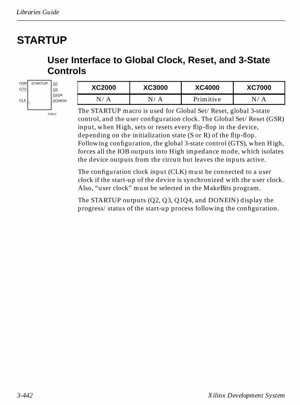
Libraries Guide
STARTUP
User Interface to Global Clock, Reset, and 3-StateControls
The STARTUP macro is used for Global Set/Reset, global 3-statecontrol, and the user configuration clock. The Global Set/Reset (GSR)input, when High, sets or resets every flip-flop in the device,depending on the initialization state (S or R) of the flip-flop.Following configuration, the global 3-state control (GTS), when High,forces all the IOB outputs into High impedance mode, which isolatesthe device outputs from the circuit but leaves the inputs active.
The configuration clock input (CLK) must be connected to a userclock if the start-up of the device is synchronized with the user clock.Also, “user clock” must be selected in the MakeBits program.
The STARTUP outputs (Q2, Q3, Q1Q4, and DONEIN) display theprogress/status of the start-up process following the configuration.
XC2000 XC3000 XC4000 XC7000
N/A N/A Primitive N/A
X3911
CLK
GTS
GSR
DONEIN
STARTUP
Q1Q4
Q3
Q2
3-442 Xilinx Development System

Design Elements
TCK
Boundary-Scan Test Clock Input Pad
The TCK input pad is connected to the boundary-scan test clock,which shifts the serial data and instructions into and out of theboundary-scan data registers. The function of the TCK pad is deviceconfiguration dependent and can be used as follows.
● During configuration TCK is connected to the boundary-scanlogic.
● After configuration, if boundary-scan is not used, the TCK pad isunrestricted and can be used by the XACT routing tools as aninput/output pad.
● After configuration, if boundary-scan is used, the TCK pad can beused for user-logic input by connecting it directly to the user logic.
XC2000 XC3000 XC4000 XC7000
N/A N/A Primitive N/AX3895
TCK
Libraries Guide 3-443
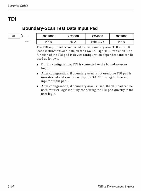
Libraries Guide
TDI
Boundary-Scan Test Data Input Pad
The TDI input pad is connected to the boundary-scan TDI input. Itloads instructions and data on the Low-to-High TCK transition. Thefunction of the TDI pad is device configuration dependent and can beused as follows.
● During configuration, TDI is connected to the boundary-scanlogic.
● After configuration, if boundary-scan is not used, the TDI pad isunrestricted and can be used by the XACT routing tools as aninput/output pad.
● After configuration, if boundary-scan is used, the TDI pad can beused for user-logic input by connecting the TDI pad directly to theuser logic.
XC2000 XC3000 XC4000 XC7000
N/A N/A Primitive N/AX3897
TDI
3-444 Xilinx Development System

Design Elements
TDO
Boundary-Scan Data Output Pad
The TDO data output pad is connected to the boundary-scan TDOoutput. It is connected to the external circuit to provide theboundary-scan data for each Low-to-High TCK transition. The func-tion of the TDO pad is device configuration dependent and can beused as follows.
● During configuration, TDO is connected to the boundary-scanlogic.
● After configuration, if boundary-scan is not used, the TDO padcan be used as a bidirectional 3-state I/O pad by the XACT rout-ing tools.
● After configuration, if boundary-scan is used, the TDO pad is stillused as an output from the boundary-scan logic.
XC2000 XC3000 XC4000 XC7000
N/A N/A Primitive N/AX3899
TDO
Libraries Guide 3-445

Libraries Guide
TIMEGRP
Schematic-Level Table of Basic Timing SpecificationGroups
The TIMEGRP primitive table defines timing groups used in “from-to” TIMESPEC statements in terms of other groups. The TIMEGRPtable is shown in the following figure.
These groups can include predefined groups, such as “ffs,” groupscreated by using TNM attributes, such as TNM-reg on schematics,and other groups defined by a statement in the TIMEGRP symbol.
The following example statement defines groups in a TIMEGRPsymbol.
=all_but_regs=ffs:except:regs
The table can contain up to 8 statements of any character length, butonly 30 characters are displayed in the symbol.
XC2000 XC3000 XC4000 XC7000
N/A Primitive Primitive N/A
X4699
TIMEGRP
3-446 Xilinx Development System

Design Elements
TIMESPEC
Schematic-Level Timing Requirement Table
* ignored in XC7000 designs
The TIMESPEC primitive is a table that specifies up to eight timingattributes (TS). TS attributes can be any length, but only 30 charactersare displayed in the TIMESPEC window. The TIMESPEC table isdisplayed in the follow figure.
XC4000 OrCAD Only Schematic-Level TimingRequirement Signal TagThe TS Signal Tag or parameter attaches timing attributes to nets inthe schematic.
Refer to the appropriate CAE tool interface user guide for detailsabout using the TIMESPEC primitive and TS Signal Tag.
XC2000 XC3000 XC4000 XC7000
N/A Primitive Primitive Primitive*
X3866
TIMESPEC
Libraries Guide 3-447

Libraries Guide
TMS
Boundary-Scan Test Mode Select Input Pad
The TMS input pad is connected to the boundary-scan TMS input. Itdetermines which boundary-scan operation is performed. The func-tion of the TMS pad is device configuration dependent and can beused as follows.
● During configuration, TMS is connected to the boundary-scanlogic.
● After configuration, if boundary-scan is not used, the TMS pad isunrestricted and can be used by the XACT routing tools as aninput/output pad.
● After configuration, if boundary-scan is used, the TMS pad can beused for user-logic input by connecting the TMS pad directly tothe user logic.
XC2000 XC3000 XC4000 XC7000
N/A N/A Primitive N/AX3901
TMS
3-448 Xilinx Development System

Design Elements
UPAD
Connects the I/O Node of an IOB to the Internal PLDCircuit
A UPAD allows the use of any unbonded IOBs in a device. It is usedthe same way as a IOPAD, except that the signal output is not visibleon any external device pins.
XC2000 XC3000 XC4000 XC7000
Primitive Primitive Primitive PrimitiveX3843
UPAD
Libraries Guide 3-449
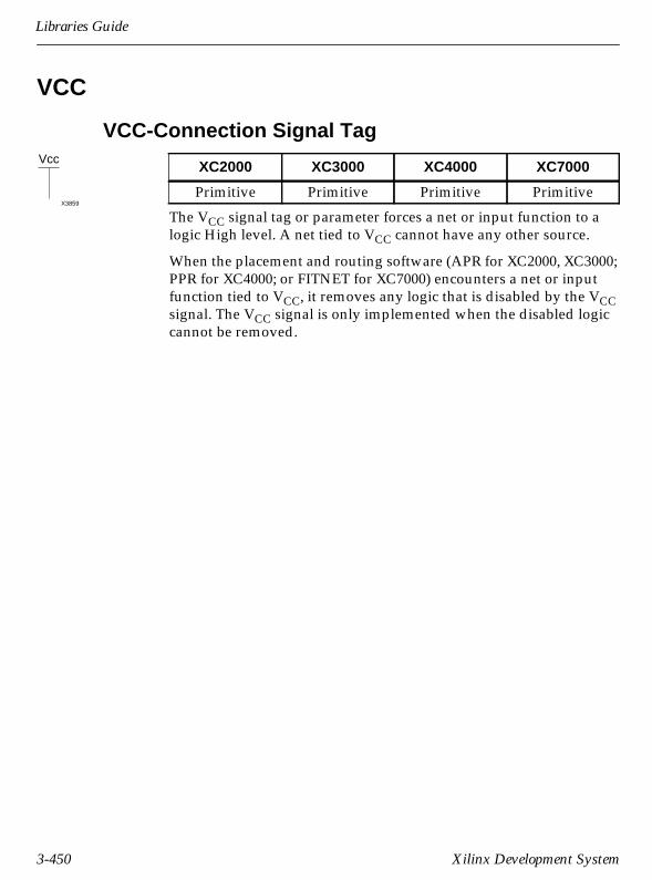
Libraries Guide
VCC
VCC-Connection Signal Tag
The VCC signal tag or parameter forces a net or input function to alogic High level. A net tied to VCC cannot have any other source.
When the placement and routing software (APR for XC2000, XC3000;PPR for XC4000; or FITNET for XC7000) encounters a net or inputfunction tied to VCC, it removes any logic that is disabled by the VCCsignal. The VCC signal is only implemented when the disabled logiccannot be removed.
XC2000 XC3000 XC4000 XC7000
Primitive Primitive Primitive PrimitiveX3859
Vcc
3-450 Xilinx Development System

Design Elements
WAND1, WAND4, WAND8, and WAND16
Open-Drain Buffers
WAND1, WAND4, WAND8, and WAND16 are single and multipleopen-drain buffers. Each buffer has an input (I) and an open-drainoutput (O). When any of the inputs is Low, the output is Low. Whenall the inputs are High, the output is off. To obtain a High output, addpull-up resistors to the output (O). One pull-up resistor uses the leastpower, and two pull-up resistors achieve the fastest Low-to-Hightransition.
To indicate two pull-up resistors, add a DOUBLE parameter to thepull-up symbol attached to the output (O) node. Refer to the appro-priate CAE tool interface user guide for details.
Figure 3-196 WAND8 XC4000 Implementation
Name XC2000 XC3000 XC4000 XC7000WAND1 N/A N/A Primitive N/AWAND4,WAND8,WAND16
N/A N/A Macro N/A
X3915
I4
I2
I1
O
WAND4
I3
X3916
O
WAND8I[7:0]
X3917
O
WAND16I[15:0]
X3905
I7
I0
I1
I2
I3
I4
I5
I6
I[7:0]
O
WAND1
WAND1
WAND1
WAND1
WAND1
WAND1
WAND1
WAND1
Libraries Guide 3-451

Libraries Guide
WOR2AND
2-Input OR Gate with Wired-AND Open-Drain BufferOutput
WOR2AND is a 2-input (I1 and I2) OR gate/buffer with an open-drain output (O). It is used in bus applications by tying multipleopen-drain outputs together. When both inputs (I1 and I2) are Low,the output (O) is Low. When either input is High, the output is off;wor2and cannot source or sink current. To establish an output Highlevel, tie a pull-up resistor(s) to the output (O). One pull-up resistoruses the least power, two pull-up resistors achieve the fastest Low-to-High speed.
To indicate two pull-up resistors, append a DOUBLE parameter tothe pull-up symbol attached to the output (O) node. Refer to theappropriate CAE tool interface user guide for details.
XC2000 XC3000 XC4000 XC7000
N/A N/A Primitive N/AX3906
3-452 Xilinx Development System

Design Elements
XNOR
2- to 9-Input XNOR Gates with Non-Inverted Inputs
* XNOR7 – XNOR9 not supported for XC7336 designs
The XNOR function is performed in the Configurable Logic Block(CLB) function generators in XC2000, XC3000, and XC4000. XNORfunctions of up to nine inputs are available. All inputs are non-inverting. Because each input uses a CLB resource, replace functionswith unused inputs with functions having the necessary number ofinputs.
Figure 3-197 XNOR8 XC2000 Implementation
Figure 3-198 XNOR8 XC3000 Implementation
Name XC2000 XC3000 XC4000 XC7000
XNOR3 – XNOR4 Primitive Primitive Primitive PrimitiveXNOR5 Macro Primitive Primitive PrimitiveXNOR6 – XNOR9 Macro Macro Macro Primitive*
XNOR2
XOR3
XNOR4
XNOR5
XNOR6
XNOR8
XNOR7
XNOR9
XOR3
XOR3
I24I3
I0I1
I47I7I6I5
OI2
I4
XNOR4
XNOR5
O
I0I1I2I3
I5I4
I47I6I7
XOR4
Libraries Guide 3-453

Libraries Guide
Figure 3-199 XNOR8 XC4000 Implementation
I5I4
I13
I47
O
I2I1
I3
I6
I0
I7
XOR4
XOR3
XNOR3
3-454 Xilinx Development System

Design Elements
XOR
2- to 9-Input XOR Gates with Non-Inverted Inputs
* XOR7 – XOR9 not supported for XC7336 designs
The XOR function is performed in the Configurable Logic Block(CLB) function generators for XC2000, XC3000, and XC4000. XORfunctions of up to nine inputs are available. All inputs are non-inverting. Because each input uses a CLB resource, replace functionswith unused inputs with functions having the necessary number ofinputs.
Figure 3-200 XOR8 XC2000 Implementation
Figure 3-201 XOR8 XC3000 Implementation
Name XC2000 XC3000 XC4000 XC7000
XOR2 – XOR4 Primitive Primitive Primitive PrimitiveXOR5 Macro Primitive Primitive PrimitiveXOR6 – XOR9 Macro Macro Macro Primitive*
XOR2
XOR3
XOR4
XOR5
XOR6
XOR7
XOR8
XOR9
I4
I2O
I5I6I7
I47
I1I0
I3 I24
XOR4
XOR3
XOR3
O
I0I1I2I3
I5I4
I47I6I7
XOR4
XOR5
Libraries Guide 3-455
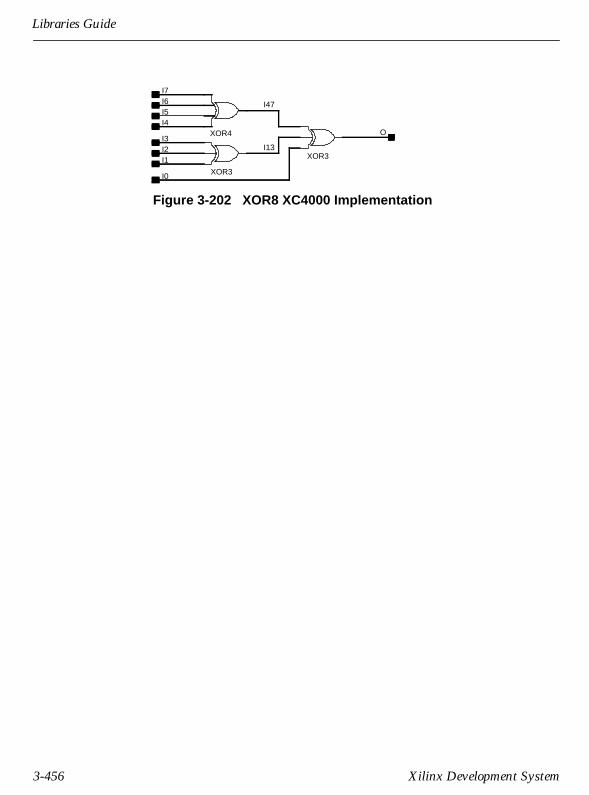
Libraries Guide
Figure 3-202 XOR8 XC4000 Implementation
I5I4
I13
I47
O
I2I1
I3
I6
I0
I7
XOR4
XOR3
XOR3
3-456 Xilinx Development System
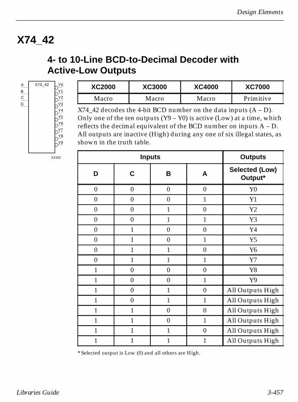
Design Elements
X74_42
4- to 10-Line BCD-to-Decimal Decoder withActive-Low Outputs
X74_42 decodes the 4-bit BCD number on the data inputs (A – D).Only one of the ten outputs (Y9 – Y0) is active (Low) at a time, whichreflects the decimal equivalent of the BCD number on inputs A – D.All outputs are inactive (High) during any one of six illegal states, asshown in the truth table.
* Selected output is Low (0) and all others are High.
XC2000 XC3000 XC4000 XC7000
Macro Macro Macro Primitive
Inputs Outputs
D C B ASelected (Low)
Output*
0 0 0 0 Y00 0 0 1 Y10 0 1 0 Y20 0 1 1 Y30 1 0 0 Y40 1 0 1 Y50 1 1 0 Y60 1 1 1 Y71 0 0 0 Y81 0 0 1 Y91 0 1 0 All Outputs High1 0 1 1 All Outputs High1 1 0 0 All Outputs High1 1 0 1 All Outputs High1 1 1 0 All Outputs High1 1 1 1 All Outputs High
X4162
X74_42
D
C
B
A
Y9
Y8
Y7
Y6
Y5
Y4
Y3
Y2
Y1
Y0
Libraries Guide 3-457

Libraries Guide
Figure 3-203 X74_42 XC2000/3000/4000 Implementation
Y9
Y8
Y7
Y6
Y5
Y4
Y3
Y2
Y1
Y0
CD
BA
NAND4B1
NAND4B3
NAND4B2
OR4
NAND4B3
NAND4B3
NAND4B3
NAND4B2
NAND4B2
NAND4B2
3-458 Xilinx Development System

Design Elements
X74_L85
4-Bit Expandable Magnitude Comparator
* not supported for XC7336 designs
X74_L85 is a 4-bit magnitude comparator that compares two 4-bitbinary-weighted words A3 – A0 and B3 – B0, where A3 and B3 arethe most significant bits. The greater-than output, AGBO, is Highwhen A>B. The less-than output, ALBO, is High when A<B, and theequal output, AEBO, is High when A=B. The expansion inputs,AGBI, ALBI, and AEBI, are the least significant bits. Words of greaterlength can be compared by cascading the comparators. The AGBO,ALBO, and AEBO outputs of the stage handling less-significant bitsare connected to the corresponding AGBI, ALBI, and AEBI inputs ofthe next stage handling more- significant bits. For proper operation,the stage handling the least significant bits must have AGBI andALBI tied Low and AEBI tied High.
XC2000 XC3000 XC4000 XC7000
Macro Macro Macro Primitive*
X4163
X74_L85
A0
ALBI
AEBI
AGBI
ALBO
AEBO
AGBO
B0
A3
A2
A1
B3
B2
B1
Libraries Guide 3-459

Libraries Guide
For XC7000, outputs differ when A=B and when more than one expansion input(AGBI, ALBI, or AEBI) is high.
Inputs Outputs
A3, B3 A2, B2 A1, B1 A0, B0 AGBI ALBI AEBI AGBO ALBO AEBO
A3>B3 X X X X X X 1 0 0A3<B3 X X X X X X 0 1 0A3=B3 A2>B2 X X X X X 1 0 0A3=B3 A2<B2 X X X X X 0 1 0A3=B3 A2=B2 A1>B1 X X X X 1 0 0A3=B3 A2=B2 A1<B1 X X X X 0 1 0A3=B3 A2=B2 A1=B1 A0>B0 X X X 1 0 0A3=B3 A2=B2 A1=B1 A0<B0 X X X 0 1 0A3=B3 A2=B2 A1=B1 A0=B0 1 0 0 1 0 0A3=B3 A2=B2 A1=B1 A0=B0 0 1 0 0 1 0A3=B3 A2=B2 A1=B1 A0=B0 0 0 1 0 0 1A3=B3 A2=B2 A1=B1 A0=B0 0 1 1 0 1 1A3=B3 A2=B2 A1=B1 A0=B0 1 0 1 1 0 1A3=B3 A2=B2 A1=B1 A0=B0 1 1 1 1 1 1A3=B3 A2=B2 A1=B1 A0=B0 1 1 0 1 1 0A3=B3 A2=B2 A1=B1 A0=B0 0 0 0 0 0 0
3-460 Xilinx Development System
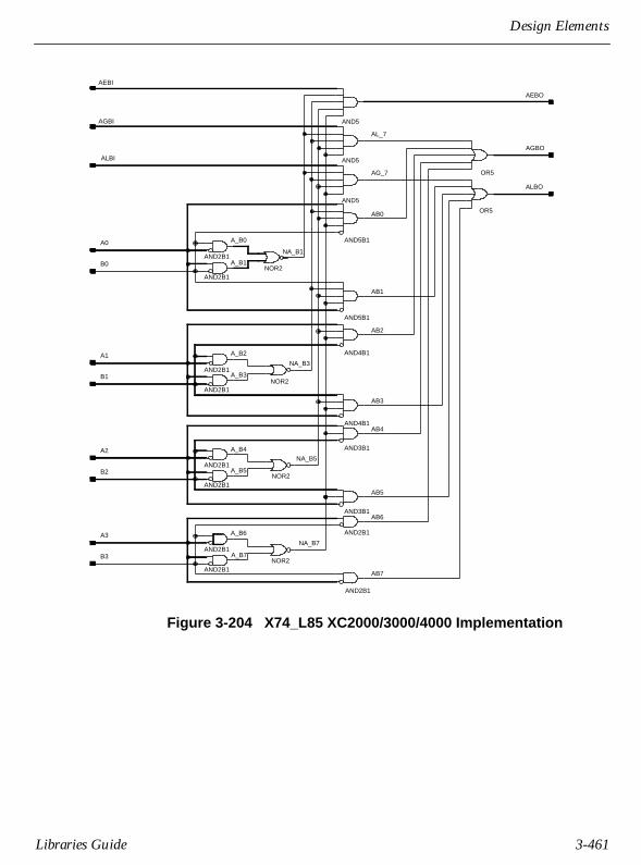
Design Elements
Figure 3-204 X74_L85 XC2000/3000/4000 Implementation
NA_B7
NOR2A_B5
A_B4
NOR2
NA_B1
B3
AGBI
ALBI
AEBI
AGBO
ALBO
A0
A1
B1
B2
A2
A3
AEBO
AND2B1
AND2B1
AND3B1
AND2B1
AND2B1
AND4B1
AND4B1
AND2B1
AND5B1
AND5B1
AND5
AND5
AND5
AND2B1
AND2B1
AND2B1
AND3B1
AND2B1
AND2B1
OR5
OR5
B0
A_B0
A_B1NOR2
NOR2
NA_B3
A_B2
A_B3
A_B7
A_B6
NA_B5
AB7
AB6
AB5
AB4
AB3
AB2
AB1
AB0
AG_7
AL_7
Libraries Guide 3-461

Libraries Guide
X74_138
3- to 8-Line Decoder/Demultiplexer with Active-LowOutputs and Three Enables
X74_138 is an expandable decoder/demultiplexer with oneactive-High enable input (G1), two active-Low enable inputs(G2A and G2B), and eight active-Low outputs (Y7 – Y0). When G1 isHigh and G2A and G2B are Low, one of the eight active-Low outputsis selected with a 3-bit binary address on address inputs A, B, and C.The non-selected outputs are High. When G1 is Low or when G2A orG2B is High, all outputs are High.
X74_138 can be used as an 8-output active-Low demultiplexer bytying the data input to one of the enable inputs.
XC2000 XC3000 XC4000 XC7000
Macro Macro Macro Primitive
Inputs Outputs
C B A G1 G2A G2B Y7 Y6 Y5 Y4 Y3 Y2 Y1 Y0
0 0 0 1 0 0 1 1 1 1 1 1 1 00 0 1 1 0 0 1 1 1 1 1 1 0 10 1 0 1 0 0 1 1 1 1 1 0 1 10 1 1 1 0 0 1 1 1 1 0 1 1 11 0 0 1 0 0 1 1 1 0 1 1 1 11 0 1 1 0 0 1 1 0 1 1 1 1 11 1 0 1 0 0 1 0 1 1 1 1 1 11 1 1 1 0 0 0 1 1 1 1 1 1 1X X X 0 X X 1 1 1 1 1 1 1 1X X X X 1 X 1 1 1 1 1 1 1 1X X X X X 1 1 1 1 1 1 1 1 1
X4164
X74_138
G1
G2B
G2A
C
B
A
Y7
Y6
Y5
Y4
Y3
Y2
Y1
Y0
3-462 Xilinx Development System

Design Elements
Figure 3-205 X74_138 XC2000/3000/4000 Implementation
Y7
Y6
Y5
Y4
Y3
Y2
Y1
Y0
Y[7:0]
C
EG2AG2B
G1
AND3B2
NAND4B3
NAND4B2
NAND4B2
NAND4B1
NAND4B2
NAND4B1
NAND4B1
NAND4
BA
Libraries Guide 3-463

Libraries Guide
X74_139
2- to 4-Line Decoder/Demultiplexer with Active-LowOutputs and Active-Low Enable
X74_139 implements one half of a standard 74139 dual 2- to 4-linedecoder/demultiplexer. When the active-Low enable input (G) isLow, one of the four active-Low outputs (Y3 – Y0) is selected with the2-bit binary address on the A and B address input lines. B is the High-order address bit. The non-selected outputs are High. Also, when G isHigh all outputs are High.
X74_139 can be used as a 4-output active-Low demultiplexer by tyingthe data input to G.
Figure 3-206 X74_139 XC2000/3000/4000 Implementation
XC2000 XC3000 XC4000 XC7000
Macro Macro Macro Primitive
Inputs Outputs
G B A Y3 Y2 Y1 Y0
0 0 0 1 1 1 00 0 1 1 1 0 10 1 0 1 0 1 10 1 1 0 1 1 11 X X 1 1 1 1
X4165
X74_139
B
Y2
Y1
Y0A
Y3G
Y0NAND3B3
Y1NAND3B2
Y2NAND3B2
Y3NAND3B1
Y0
Y1
Y2
Y3
A
B
G
3-464 Xilinx Development System

Design Elements
X74_147
10- to 4-Line Priority Encoder with Active-Low Inputsand Outputs
X74_147 is a 10-line-to-BCD-priority encoder that accepts data fromnine active-Low inputs (I9 – I1) and produces a binary-coded decimal(BCD) representation on the four active-Low outputs A, B, C, and D.The data inputs are weighted, so when more than one input is active,only the one with the highest priority is encoded, with I9 having thehighest priority. Only nine inputs are provided, because the implied“zero” condition requires no data input. “Zero” is encoded when alldata inputs are High.
XC2000 XC3000 XC4000 XC7000
Macro Macro Macro Primitive
Inputs Outputs
I9 I8 I7 I6 I5 I4 I3 I2 I1 D C B A
1 1 1 1 1 1 1 1 0 1 1 1 01 1 1 1 1 1 1 0 X 1 1 0 11 1 1 1 1 1 0 X X 1 1 0 01 1 1 1 1 0 X X X 1 0 1 11 1 1 1 0 X X X X 1 0 1 01 1 1 0 X X X X X 1 0 0 11 1 0 X X X X X X 1 0 0 01 0 X X X X X X X 0 1 1 10 X X X X X X X X 0 1 1 01 1 1 1 1 1 1 1 1 1 1 1 1
X4166
X74_147
I9
I8
I7
I6
I5
I4
I3
I2I1
D
C
B
A
Libraries Guide 3-465
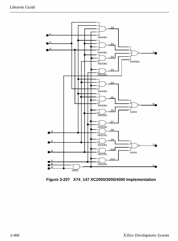
Libraries Guide
Figure 3-207 X74_147 XC2000/3000/4000 Implementation
AND2B1
AND2B1
AND2B1
NOR4
AND2B1
AND2B1
AND2B1
AND2B1
NOR4
AND4B1
AND5B1
AND4B1
AND3B1
AND4B1
NOR5B1
AND2
CI5
I4
I6
I7
I3
I2
I1
A
B
I8D
I9
D0
D1
D2
D3
D4
D5
D6
D7
D8
D9
D10
D11
3-466 Xilinx Development System
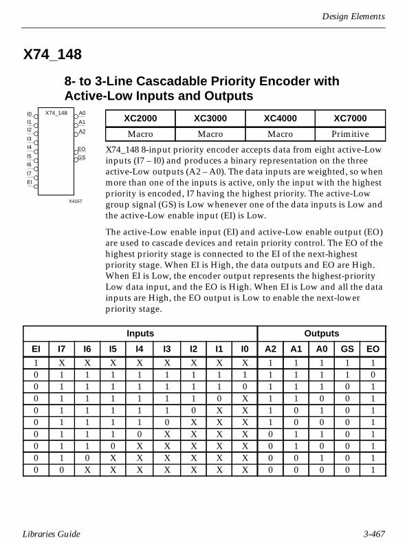
Design Elements
X74_148
8- to 3-Line Cascadable Priority Encoder withActive-Low Inputs and Outputs
X74_148 8-input priority encoder accepts data from eight active-Lowinputs (I7 – I0) and produces a binary representation on the threeactive-Low outputs (A2 – A0). The data inputs are weighted, so whenmore than one of the inputs is active, only the input with the highestpriority is encoded, I7 having the highest priority. The active-Lowgroup signal (GS) is Low whenever one of the data inputs is Low andthe active-Low enable input (EI) is Low.
The active-Low enable input (EI) and active-Low enable output (EO)are used to cascade devices and retain priority control. The EO of thehighest priority stage is connected to the EI of the next-highestpriority stage. When EI is High, the data outputs and EO are High.When EI is Low, the encoder output represents the highest-priorityLow data input, and the EO is High. When EI is Low and all the datainputs are High, the EO output is Low to enable the next-lowerpriority stage.
XC2000 XC3000 XC4000 XC7000
Macro Macro Macro Primitive
Inputs Outputs
EI I7 I6 I5 I4 I3 I2 I1 I0 A2 A1 A0 GS EO
1 X X X X X X X X 1 1 1 1 10 1 1 1 1 1 1 1 1 1 1 1 1 00 1 1 1 1 1 1 1 0 1 1 1 0 10 1 1 1 1 1 1 0 X 1 1 0 0 10 1 1 1 1 1 0 X X 1 0 1 0 10 1 1 1 1 0 X X X 1 0 0 0 10 1 1 1 0 X X X X 0 1 1 0 10 1 1 0 X X X X X 0 1 0 0 10 1 0 X X X X X X 0 0 1 0 10 0 X X X X X X X 0 0 0 0 1
X4167
X74_148
EI
I7
I6
I5
I4
I3
I2I1
A2
A1
A0I0
EO
GS
Libraries Guide 3-467
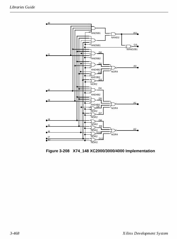
Libraries Guide
Figure 3-208 X74_148 XC2000/3000/4000 Implementation
EII7
NOR2
NAND2B1
AND5B2
AND4B2
AND3B2
NOR2
AND4B2
AND4B2
NOR2
NOR2
NOR2
NOR2
NOR2
NOR4
NOR4
NOR4
I6
A1
GS
D3
D1
D0
D2
A2
D8
D9
D10
D11
D4
D5
D6
D7
A0
EO
I2
I3
I1
I0
I4
I5
AND5B1
AND5B1
NAND2
3-468 Xilinx Development System

Design Elements
X74_150
16-to-1 Multiplexer with Active-Low Enable andOutput
When the active-Low enable input (G) is Low, the X74_150 multi-plexer chooses one data bit from 16 sources (E15 – E0) under thecontrol of select inputs A, B, C, and D. The active-Low output (W)reflects the inverse of the selected input, as shown in the truth table.When the enable input (G) is High, the output (W) is High.
XC2000 XC3000 XC4000 XC7000
Macro Macro Macro Primitive
Inputs Outputs
G D C B ASelected Input Appears
(Inverted) on W
1 X X X X 10 0 0 0 0 E00 0 0 0 1 E10 0 0 1 0 E20 0 0 1 1 E30 0 1 0 0 E40 0 1 0 1 E50 0 1 1 0 E60 0 1 1 1 E70 1 0 0 0 E80 1 0 0 1 E90 1 0 1 0 E100 1 0 1 1 E110 1 1 0 0 E120 1 1 0 1 E130 1 1 1 0 E140 1 1 1 1 E15
X4168
X74_150
E9
E8
E7
E6
E5
E4
E3
E2
E1
E0
D
C
B
A
E15
E14
E13
E12
E11
E10
G
W
Libraries Guide 3-469

Libraries Guide
Figure 3-209 X74_150 XC2000/3000/4000 Implementation
M8F
D0D1 O
S0
M2_1M8B
D0D1 O
S0
M2_1
MCF
D0D1 O
S0
M2_1
MEF
D0D1 O
S0
M2_1MCD
D0D1 O
S0
M2_1
MAB
D0D1 O
S0
M2_1M89
D0D1 O
S0
M2_1
AND3B1
AND3B2
M07
D0D1 O
S0
M2_1
M67
D0D1 O
S0
M2_1M45
D0D1 O
S0
M2_1
M47
D0D1 O
S0
M2_1
M03
D0D1 O
S0
M2_1
M23
D0D1 O
S0
M2_1M01
D0D1 O
S0
M2_1
W
XNOR2M8F
M07
E15E14
E13E12
E11E10
E9E8
E7E6
E5E4
E3E2
E1E0
M23M01
M45M67
M89MAB
MCDMEF
M47M03
M8BMCF
ABCDG
3-470 Xilinx Development System

Design Elements
X74_151
8-to-1 Multiplexer with Active-Low Enable andComplementary Outputs
When the active-Low enable (G) is Low, the X74_151 multiplexerchooses one data bit from eight sources (D7 – D0) under control of theselect inputs A, B, and C. The output (Y) reflects the state of theselected input, and the active-Low output (W) reflects the inverse ofthe selected input as shown in the truth table. When G is High, the Youtput is Low, and the W output is High.
XC2000 XC3000 XC4000 XC7000
Macro Macro Macro Primitive
Inputs Outputs
G C B A Y W
1 X X X 1 00 0 0 0 D0 D00 0 0 1 D1 D10 0 1 0 D2 D20 0 1 1 D3 D30 1 0 0 D4 D40 1 0 1 D5 D50 1 1 0 D6 D60 1 1 1 D7 D7
X4169
X74_151
D3
D2
D1
D7
D6
D5
D4
C
B
A
W
D0
G
Y
Libraries Guide 3-471

Libraries Guide
Figure 3-210 X74_151 XC2000/3000/4000 Implementation
A
YD1D0
O
ES0
M2_1E
M47
D0D1
O
S0
M2_1
M03
D0D1
O
S0
M2_1
M67
D0D1
O
S0
M2_1M45
D0D1
O
S0
M2_1
M23
D0D1
O
S0
M2_1M01
D0D1
O
S0
M2_1
M23
D2
D4D5
D3
D6D7
M45M67
M47M03
BCG
WY
E
INV
INV
M01D1D0
3-472 Xilinx Development System
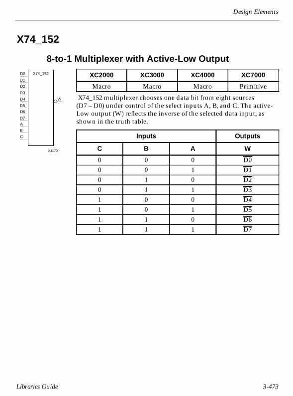
Design Elements
X74_152
8-to-1 Multiplexer with Active-Low Output
X74_152 multiplexer chooses one data bit from eight sources(D7 – D0) under control of the select inputs A, B, and C. The active-Low output (W) reflects the inverse of the selected data input, asshown in the truth table.
XC2000 XC3000 XC4000 XC7000
Macro Macro Macro Primitive
Inputs Outputs
C B A W
0 0 0 D00 0 1 D10 1 0 D20 1 1 D31 0 0 D41 0 1 D51 1 0 D61 1 1 D7
X4170
X74_152
D3
D2
D1
D0
D7
D6
D5
D4
C
B
A
W
Libraries Guide 3-473
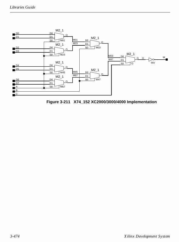
Libraries Guide
Figure 3-211 X74_152 XC2000/3000/4000 Implementation
B
D7
M03
M47 O
C
INV
A
D0
D2
D1
D4
D5
D3
D6
M23
M01
M45
M67
W
M01
D0
D1O
S0
M2_1
M23
D0
D1O
S0
M2_1
M45
D0
D1O
S0
M2_1
M67
D0
D1O
S0
M2_1
M03
D0
D1O
S0
M2_1
M47
D0
D1O
S0
M2_1
O
D0
D1O
S0
M2_1
3-474 Xilinx Development System
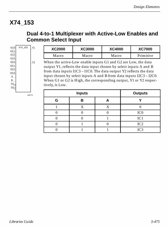
Design Elements
X74_153
Dual 4-to-1 Multiplexer with Active-Low Enables andCommon Select Input
When the active-Low enable inputs G1 and G2 are Low, the dataoutput Y1, reflects the data input chosen by select inputs A and Bfrom data inputs I1C3 – I1C0. The data output Y2 reflects the datainput chosen by select inputs A and B from data inputs I2C3 – I2C0.When G1 or G2 is High, the corresponding output, Y1 or Y2 respec-tively, is Low.
XC2000 XC3000 XC4000 XC7000
Macro Macro Macro Primitive
Inputs Outputs
G B A Y
1 X X 00 0 0 IC00 0 1 IC10 1 0 IC20 1 1 IC3
X4171
X74_153
I1C3
I1C2
I1C1
I2C3
I2C2
I2C1
I2C0
G1
B
A
Y2
I1C0
G2
Y1
Libraries Guide 3-475

Libraries Guide
Figure 3-212 X74_153 XC2000/3000/4000 Implementation
Y2
D1
D0O
E
S0
M2_1E
Y1
D1
D0O
E
S0
M2_1E
M2_23
D0
D1O
S0
M2_1
M2_01M2_01
D0
D1O
S0
M2_1
M1_23
D0
D1O
S0
M2_1
M1_01
D0
D1O
S0
M2_1
INV
INV
E1
Y1
G1
G2
B
E2
I2C3
I2C1
A
M1_01
M1_23
M2_23
I2C2
I1C1
I1C3
Y2
I1C0
I1C2
I2C0
3-476 Xilinx Development System

Design Elements
X74_154
4- to 16-Line Decoder/Demultiplexer with TwoEnables and Active-Low Outputs
When the active-Low enable inputs G1 and G2 of the X74_154decoder/demultiplexer are Low, one of 16 active-Low outputs,Y15 – Y0, is selected under the control of four binary address inputsA, B, C, and D. The non-selected inputs are High. Also, when eitherinput G1 or G2 is High, all outputs are High.
The X74_154 can be used as a 16-to-1 demultiplexer by tying the datainput to one of the G inputs and tying the other G input Low.
XC2000 XC3000 XC4000 XC7000
Macro Macro Macro Primitive
Inputs Outputs
G1 G2 D C B A Y15 Y14 Y13 Y12 Y11 Y10 Y9 ... Y0
1 X X X X X 1 1 1 1 1 1 1 ... 1X 1 X X X X 1 1 1 1 1 1 1 ... 10 0 1 1 1 1 0 1 1 1 1 1 1 ... 10 0 1 1 1 0 1 0 1 1 1 1 1 ... 10 0 1 1 0 1 1 1 0 1 1 1 1 ... 1- - - - - - - - - - - - - ... -- - - - - - - - - - - - - ... -- - - - - - - - - - - - - ... -0 0 0 0 0 0 1 1 1 1 1 1 1 ... 0
X4172
X74_154
Y9
Y8
Y7
Y6
Y5
Y4
Y3
Y2
Y1
Y0
Y15
Y14
Y13
Y12
Y11
Y10
A
C
B
D
G1
G2
Libraries Guide 3-477

Libraries Guide
Figure 3-213 X74_154 XC2000/3000/4000 Implementation
NOR2
NAND5
NAND5B1
NAND5B1
NAND5B1
NAND5B1
NAND5B2
NAND5B2
NAND5B2
NAND5B2
NAND5B2
NAND5B2
NAND5B3
NAND5B3
NAND5B3
NAND5B3
NAND5B4
G2G1
Y14
Y13
Y12
Y11
Y10
Y9
Y8
Y7
Y6
Y5
Y4
Y3
Y2
Y1
Y0
Y[15:0]
Y15AB
DC
3-478 Xilinx Development System

Design Elements
X74_157
Quadruple 2-to-1 Multiplexer with Common Selectand Active-Low Enable
When the active-Low enable input (G) is Low, a 4-bit word is selectedfrom one of two sources (A3 – A0 or B3 – B0) under the control of theselect input (S) and is reflected on the four outputs (Y4 – Y1). When Sis Low, the outputs reflect A3 – A0; when S is High, the outputsreflect B3 – B0. When G is High, the outputs are Low.
Figure 3-214 X74_157 XC2000/3000/4000 Implementation
XC2000 XC3000 XC4000 XC7000
Macro Macro Macro Primitive
Inputs Outputs
G S B A Y
1 X X X 00 1 1 X 10 1 0 X 00 0 X 1 10 0 X 0 0
X4173
X74_157
G
S
B4
A4
B3
A3
B2
A2
B1
A1
Y4
Y3
Y2
Y1
INV
A1Y1
Y2
Y4
Y3
EG
S
B4
A4
B3
A3
B2
A2
B1
Y1
D1
D0O
E
S0
M2_1E
Y2
D1
D0O
E
S0
M2_1E
Y3
D1
D0O
E
S0
M2_1E
Y4
D1
D0O
E
S0
M2_1E
Libraries Guide 3-479

Libraries Guide
X74_158
Quadruple 2-to-1 Multiplexer with Common Select,Active-Low Enable, and Active-Low Outputs
When the active-Low enable (G) is Low, a 4-bit word is selected fromone of two sources (A3 – A0 or B3 – B0) under the control of thecommon select input (S). The inverse of the selected word is reflectedon the active-Low outputs (Y4 – Y1). When S is Low, A3 – A0 appearon the outputs; when S is High, B3 – B0 appear on the outputs. WhenG is High, the outputs are High.
Figure 3-215 X74_158 XC2000/3000/4000 Implementation
XC2000 XC3000 XC4000 XC7000
Macro Macro Macro Primitive
Inputs Outputs
G S B A Y
1 X X X 10 1 1 X 00 1 0 X 10 0 X 1 00 0 X 0 1
X4174
X74_158
G
S
B4
A4
B3
A3
B2
A2
B1
A1
Y4
Y3
Y2
Y1
Y4
Y3
Y2
Y1
O4
O3
O2
O1
INV
INV
G
B1
A2B2
A3B3
A4B4S
E
A1
INV
INV
INV
O1D1D0
O
ES0
M2_1E
O2D1D0
O
ES0
M2_1E
O3D1D0
O
ES0
M2_1E
O4D1D0
O
ES0
M2_1E
3-480 Xilinx Development System

Design Elements
X74_160
4-Bit BCD Counter with Parallel and Trickle Enables,Active-Low Load Enable, and Asynchronous Clear
X74_160 is a 4-stage, 4-bit, synchronous, loadable, resettable, cascad-able, binary-coded decimal (BCD) counter. The active-Low asynchro-nous clear (CLR), when Low, overrides all other inputs and resets thedata (QD, QC, QB, QA) and ripple carry-out (RCO) outputs Lowduring the Low-to-High clock (C) transition. When the active-Lowload enable input (LOAD) is Low, parallel clock enable (ENP), andtrickle clock enable (ENT) are overridden and data on inputs A, B, C,and D are loaded into the counter during the Low-to-High clock tran-sition. The data outputs (QD, QC, QB, QA) increment when ENP,ENT LOAD, and CLR are High during the Low-to-High clock transi-tion. The counter ignores clock transitions when ENP or ENT areLow and LOAD is High. RCO is High when QD, QA, and ENT areHigh and QC and QB are Low.
RCO = (QD•QC•QB•QA•ENT)
d – a = state of referenced input one set-up time prior to active clock transition
The carry-lookahead design allows cascading of large counterswithout extra gating. Both ENT and ENP must be High to count. ENTis fed forward to enable RCO, which produces a High output pulsewith the approximate duration of the QA output. The followingfigure illustrates a carry-lookahead design.
XC2000 XC3000 XC4000 XC7000
Macro Macro Macro Primitive
Inputs Outputs
CLR LOAD ENP ENT D – A CK QD – QA RCO
0 X X X X X 0 01 0 X X D – A ↑ d – a RCO1 1 0 X X X No Chg RCO1 1 X 0 X X No Chg 01 1 1 1 X ↑ Inc RCO
X4175
X74_160
QD
QC
QB
QA
CK
ENT
ENP
LOAD
D
C
B
A
RCO
CLR
Libraries Guide 3-481

Libraries Guide
Figure 3-216 Carry-Lookahead Design
The RCO output of the first stage of the ripple carry is connected tothe ENP input of the second stage and all subsequent stages. TheRCO output of the second stage and all subsequent stages isconnected to the ENT input of the next stage. The ENT of the secondstage is always enabled/tied to VCC. CE is always connected to theENT input of the first stage. This cascading method allows the firststage of the ripple carry to be built as a prescaler. In other words, thefirst stage is built to count very fast.
The counter recovers from any of six possible illegal states andreturns to a normal count sequence within two clock cycles.
X4719
ENT
ENP
RCO
ENT
ENP
RCO
ENT
ENP
RCOVcc
Vcc
ENTCE
ENP
RCO
3-482 Xilinx Development System

Design Elements
Figure 3-217 X74_160 XC2000/3000/4000 Implementation
RCO
TQAD
AND3
AND5B2
QB
QC
D
C
B
CLR
CK
LOADA
CLRB
LB
CEENP
T1
T2TQB
T3
AND2
INV
AND3
AND3B1
QA
CET
CLR
QLD
C
FTCLE
QD
CET
CLR
QLD
C
FTCLE
QC
CET
CLR
QLD
C
FTCLE
QB
CET
CLR
QLD
C
FTCLE
VCC
AND2 OR2
INV
QD
QA
ENT
X74_160.4K
Libraries Guide 3-483
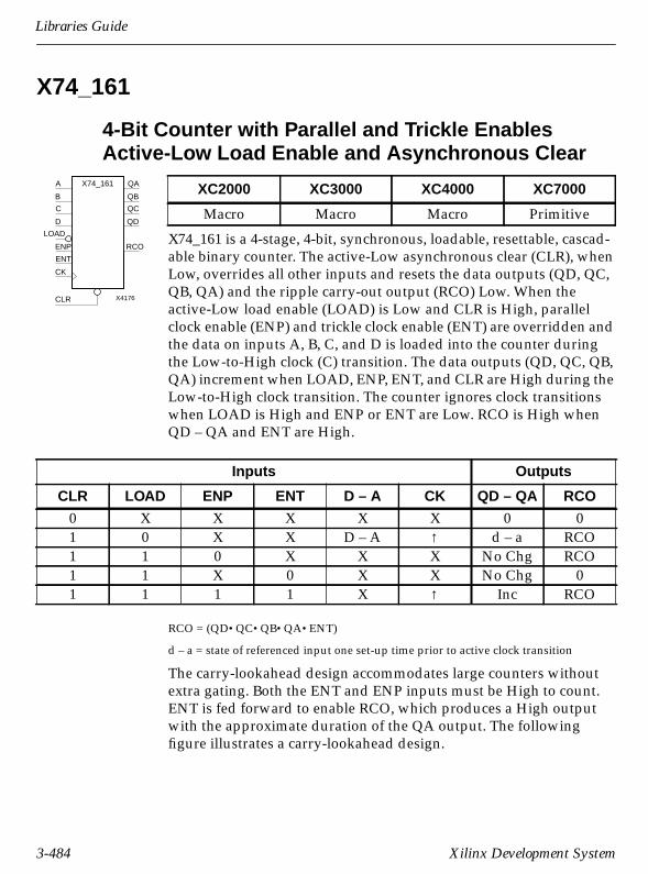
Libraries Guide
X74_161
4-Bit Counter with Parallel and Trickle EnablesActive-Low Load Enable and Asynchronous Clear
X74_161 is a 4-stage, 4-bit, synchronous, loadable, resettable, cascad-able binary counter. The active-Low asynchronous clear (CLR), whenLow, overrides all other inputs and resets the data outputs (QD, QC,QB, QA) and the ripple carry-out output (RCO) Low. When theactive-Low load enable (LOAD) is Low and CLR is High, parallelclock enable (ENP) and trickle clock enable (ENT) are overridden andthe data on inputs A, B, C, and D is loaded into the counter duringthe Low-to-High clock (C) transition. The data outputs (QD, QC, QB,QA) increment when LOAD, ENP, ENT, and CLR are High during theLow-to-High clock transition. The counter ignores clock transitionswhen LOAD is High and ENP or ENT are Low. RCO is High whenQD – QA and ENT are High.
RCO = (QD•QC•QB•QA•ENT)
d – a = state of referenced input one set-up time prior to active clock transition
The carry-lookahead design accommodates large counters withoutextra gating. Both the ENT and ENP inputs must be High to count.ENT is fed forward to enable RCO, which produces a High outputwith the approximate duration of the QA output. The followingfigure illustrates a carry-lookahead design.
XC2000 XC3000 XC4000 XC7000
Macro Macro Macro Primitive
Inputs Outputs
CLR LOAD ENP ENT D – A CK QD – QA RCO
0 X X X X X 0 01 0 X X D – A ↑ d – a RCO1 1 0 X X X No Chg RCO1 1 X 0 X X No Chg 01 1 1 1 X ↑ Inc RCO
X4176
X74_161
QD
QC
QB
QA
CK
ENT
ENP
LOAD
D
C
B
A
RCO
CLR
3-484 Xilinx Development System
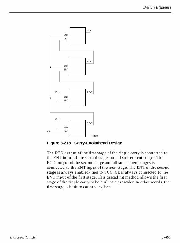
Design Elements
Figure 3-218 Carry-Lookahead Design
The RCO output of the first stage of the ripple carry is connected tothe ENP input of the second stage and all subsequent stages. TheRCO output of the second stage and all subsequent stages isconnected to the ENT input of the next stage. The ENT of the secondstage is always enabled/tied to VCC. CE is always connected to theENT input of the first stage. This cascading method allows the firststage of the ripple carry to be built as a prescaler. In other words, thefirst stage is built to count very fast.
X4719
ENT
ENP
RCO
ENT
ENP
RCO
ENT
ENP
RCOVcc
Vcc
ENTCE
ENP
RCO
Libraries Guide 3-485

Libraries Guide
Figure 3-219 X74_161 XC2000/3000/4000 Implementation
LOADB
CLRB
LOAD
INV
CK
CLR
AND5
QA
QB
QC
QD
ENP
AND2
ENT
D
C
B
AVCC
T2
AND2
AND3
T3
RCOQ3
CE
T
CLR
Q
L
D
C
FTCLE
Q2
CE
T
CLR
Q
L
D
C
FTCLE
Q1
CE
T
CLR
Q
L
D
C
FTCLE
Q0
CE
T
CLR
Q
L
D
C
FTCLE
CE
INV
3-486 Xilinx Development System

Design Elements
X74_162
4-Bit Counter with Parallel and Trickle Enables andActive-Low Load Enable and Synchronous Reset
X74_162 is a 4-stage, 4-bit, synchronous, loadable, resettable, cascad-able binary-coded decimal (BCD) counter. The active-Low synchro-nous reset (R), when Low, overrides all other inputs and resets thedata (QD, QC, QB, QA) and ripple carry-out (RCO) outputs Lowduring the Low-to-High clock (C) transition. When the active-Lowload enable input (LOAD) is Low, parallel clock enable (ENP) andtrickle clock enable (ENT) are overridden and data on inputs A, B, C,and D is loaded into the counter during the Low-to-High clock transi-tion. The data outputs (QD, QC, QB, QA) increment when ENP, ENT,LOAD, and R are High during the Low-to-High clock transition. Thecounter ignores clock transitions when ENP or ENT are Low andLOAD is High. RCO is High when QD, QA, and ENT are High andQC and QB are Low.
RCO = (QD•QC•QB•QA•ENT)
d – a = state of referenced input one set-up time prior to active clock transition
The carry-lookahead design accommodates cascading large counterswithout extra gating. Both ENT and ENP must be High to count. TheENT is fed forward to enable RCO, which produces a High outputpulse with the approximate duration of the QA output. Thefollowing figure illustrates a carry-lookahead design.
XC2000 XC3000 XC4000 XC7000
Macro Macro Macro Primitive
Inputs Outputs
R LOAD ENP ENT D – A CK QD – QA RCO
0 X X X X ↑ 0 01 0 X X D – A ↑ d – a RCO1 1 0 X X X No Chg RCO1 1 X 0 X X No Chg 01 1 1 1 X ↑ Inc RCO
X4177
X74_162
QD
QC
QB
QA
CK
ENT
ENP
LOAD
D
C
B
A
RCO
R
Libraries Guide 3-487

Libraries Guide
Figure 3-220 Carry-Lookahead Design
The RCO output of the first stage of the ripple carry is connected tothe ENP input of the second stage and all subsequent stages. TheRCO output of the second stage and all subsequent stages isconnected to the ENT input of the next stage. The ENT of the secondstage is always enabled/tied to VCC. CE is always connected to theENT input of the first stage. This cascading method allows the firststage of the ripple carry to be built as a prescaler. In other words, thefirst stage is built to count very fast.
The counter recovers from any of six possible illegal states andreturns to a normal count sequence within two clock cycles.
X4719
ENT
ENP
RCO
ENT
ENP
RCO
ENT
ENP
RCOVcc
Vcc
ENTCE
ENP
RCO
3-488 Xilinx Development System

Design Elements
Figure 3-221 X74_162 XC2000/3000/4000 Implementation
RCO
AND5B2
QA
QD
ENT
QC
QB
B
QD
FTRSLE
CET
S
R
QLD
C
D
RB
LB
CE T2 TQBT3
AND2 AND3AND2 OR2
C
INV
VCC
AND3B1
INV
T1
QB
FTRSLE
CET
S
R
QLD
C
QA
FTRSLE
CET
S
R
QLD
C
LOADA
CK
R
ENP
GND
AND3
TQAD
QC
FTRSLE
CET
S
R
QLD
C
X74_162.4K
Libraries Guide 3-489

Libraries Guide
X74_163
4-Bit Counter with Parallel and Trickle Enables,Active-Low Load Enable, and Synchronous Reset
X74_163 is a 4-stage, 4-bit, synchronous, loadable, resettable, cascad-able binary counter. The active-Low synchronous reset (R), whenLow, overrides all other inputs and resets the data outputs (QD, QC,QB, QA) and the ripple carry-out output (RCO) Low. When theactive-Low load enable (LOAD) is Low and R is High, parallel clockenable (ENP) and trickle clock enable (ENT) are overridden and thedata on inputs (A, B, C, D) is loaded into the counter during the Low-to-High clock (C) transition. The outputs (QD, QC, QB, QA) incre-ment when LOAD, ENP, ENT, and R are High during the Low-to-High clock transition. The counter ignores clock transitions whenLOAD is High and ENP or ENT are Low; RCO is High whenQD – QA and ENT are High.
RCO = (QD•QC•QB•QA•ENT)
d – a = state of referenced input one set-up time prior to active clock transition
The carry-lookahead design accommodates large counters withoutextra gating. Both the ENT and ENP inputs must be High to count.ENT is propagated forward to enable RCO, which produces a Highoutput with the approximate duration of the QA output. Thefollowing figure illustrates a carry-lookahead design.
XC2000 XC3000 XC4000 XC7000
Macro Macro Macro Primitive
Inputs Outputs
R LOAD ENP ENT D – A CK QD – QA RCO
0 X X X X ↑ 0 01 0 X X D – A ↑ d – a RCO1 1 0 X X X No Chg RCO1 1 X 0 X X No Chg 01 1 1 1 X ↑ Inc RCO
X4178
X74_163
QD
QC
QB
QA
CK
ENT
ENP
LOAD
D
C
B
A
RCO
R
3-490 Xilinx Development System

Design Elements
Figure 3-222 Carry-Lookahead Design
The RCO output of the first stage of the ripple carry is connected tothe ENP input of the second stage and all subsequent stages. TheRCO output of the second stage and all subsequent stages isconnected to the ENT input of the next stage. The ENT of the secondstage is always enabled/tied to VCC. CE is always connected to theENT input of the first stage. This cascading method allows the firststage of the ripple carry to be built as a prescaler. In other words, thefirst stage is built to count very fast.
X4719
ENT
ENP
RCO
ENT
ENP
RCO
ENT
ENP
RCOVcc
Vcc
ENTCE
ENP
RCO
Libraries Guide 3-491
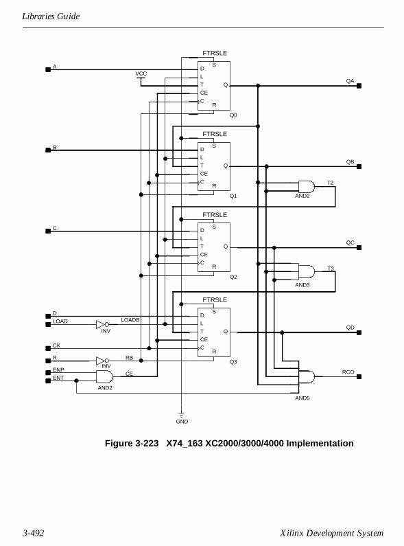
Libraries Guide
Figure 3-223 X74_163 XC2000/3000/4000 Implementation
LOADBLOAD
INV
INV
AND2
ENPCE
Q0
C
D
L
Q
R
S
T
CE
FTRSLE
RB
CK
R
QB
QC
QD
D
C
B
AVCC
T2
AND2
AND3
RCO
QA
T3
Q1
C
D
L
Q
R
S
T
CE
FTRSLE
Q2
C
D
L
Q
R
S
T
CE
FTRSLE
GND
Q3
C
D
L
Q
R
S
T
CE
FTRSLE
ENT
AND5
3-492 Xilinx Development System

Design Elements
X74_164
8-Bit Serial-In Parallel-Out Shift Register withActive-Low Asynchronous Clear
X74_164 is an 8-bit, serial input (A and B), parallel output (QH – QA)shift register with an active-Low asynchronous clear (CLR) input.The asynchronous CLR, when Low, overrides the clock input and setsthe data outputs (QH – QA) Low. When CLR is High, the AND func-tion of the two data inputs (A and B) is loaded into the first bit of theshift register during the Low-to-High clock (C) transition andappears on the QA output. During subsequent Low-to-High clocktransitions, with CLR High, the data is shifted to the next-highest bitposition as new data is loaded into QA (A and B➝QA, QA➝QB,QB➝QC, and so forth).
Registers can be cascaded by connecting the QH output of one stageto the A input of the next stage, by tying B High, and by connectingthe clock and CLR inputs in parallel.
qA – qG = state of referenced output one set-up time prior to active clocktransition
XC2000 XC3000 XC4000 XC7000
Macro Macro Macro Primitive
Inputs Outputs
CLR A B CK QA QB – QH
0 X X X 0 01 1 1 ↑ 1 qA – qG1 0 X ↑ 0 qA – qG1 X 0 ↑ 0 qA – qG
X4179
X74_164
QD
QC
QB
QA
B
A
CLR
QH
QG
QF
QE
CK
Libraries Guide 3-493

Libraries Guide
Figure 3-224 X74_164 XC2000/3000/4000 Implementation
QH
FDCE
QD
CLR
CE
C
QG
FDCE
QD
CLR
CE
C
QF
FDCE
QD
CLR
CE
C
QE
FDCE
QD
CLR
CE
C
QD
FDCE
QD
CLR
CE
C
QC
FDCE
QD
CLR
CE
C
QB
FDCE
QD
CLR
CE
C
QH
QG
QF
QE
QD
QC
QB
QAB
A
CLR
CK
VCC
INV
QA
FDCE
QD
CLR
CE
C
CLRB
AND2
SLI
3-494 Xilinx Development System

Design Elements
X74_165S
8-Bit Loadable Serial/Parallel-In Parallel-Out ShiftRegister with Clock Enable
X74_165S is an 8-bit shift register with serial-input (SI), parallel-inputs (H – A), parallel-outputs (QH – QA), and two controlinputs – clock enable (CE) and active-Low shift/load enable (S_L).When S_L is Low, data on the H – A inputs is loaded into the corre-sponding QH – QA bits of the register on the Low-to-High clock (C)transition. When CE and S_L are High, data on the SI input is loadedinto the first bit of the register during the Low-to-High clock transi-tion. During subsequent Low-to-High clock transitions, with CE andS_L High, the data is shifted to the next-highest bit position (shiftright) as new data is loaded into QA (SI➝QA, QA➝QB, QB➝QC,and so forth). The register ignores clock transitions when CE is Lowand S_L is High.
Registers can be cascaded by connecting the QH output of one stageto the SI input of the next stage and connecting clock, CE, and S_Linputs in parallel.
si, qn represent state of referenced input or output one set-up time prior to activeclock transition.
XC2000 XC3000 XC4000 XC7000
Macro Macro Macro Primitive
Inputs Outputs
S_L CE SI A – H CK QA QB – QH
0 X X A – H ↑ qa qb – qh1 0 X X X --No Change---1 1 SI X ↑ si qA – qG
X4180
X74_165S
C
B
A
G
F
E
D
CE
S_LH
QD
SI
CK
QC
QB
QA
QF
QG
QH
QE
Libraries Guide 3-495
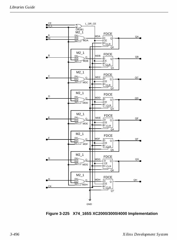
Libraries Guide
Figure 3-225 X74_165S XC2000/3000/4000 Implementation
L_OR_CE
OR2B1
AQA
QB
QC
QD
QE
QF
QG
S_L
QH
CK
CE
MDA
MDB
MDD
MD2
MDH
MDG
MDF
MDE
GND
Q0
FDCEQD
CLR
CEC
MDC
D0D1
O
S0
M2_1
MDB
D0D1 O
S0
M2_1
MDA
D0D1S0
M2_1
Q3
FDCE
QD
CLR
CEC
Q2
FDCEQD
CLR
CEC
Q1
FDCEQD
CLR
CEC
Q4
FDCEQD
CLRCEC
Q6
FDCEQD
CLRCEC
Q7
FDCEQD
CLR
CEC
MDF
D0D1
O
S0
M2_1
MDH
D0D1
O
S0
M2_1
MDG
D0D1
O
S0
M2_1
Q5
FDCE
QD
CLR
CEC
MDD
D0D1 O
S0
M2_1
MDE
D0D1
O
S0
M2_1
B
C
D
E
F
G
H
SI
3-496 Xilinx Development System
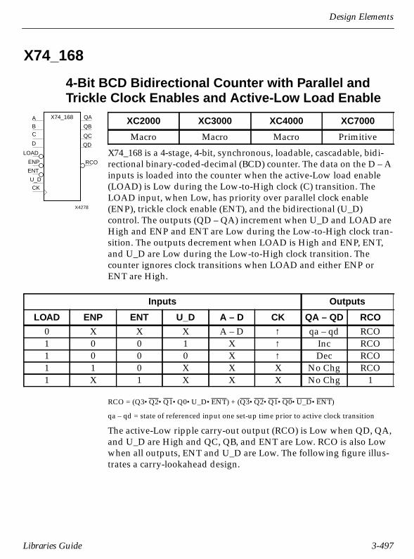
Design Elements
X74_168
4-Bit BCD Bidirectional Counter with Parallel andTrickle Clock Enables and Active-Low Load Enable
X74_168 is a 4-stage, 4-bit, synchronous, loadable, cascadable, bidi-rectional binary-coded-decimal (BCD) counter. The data on the D – Ainputs is loaded into the counter when the active-Low load enable(LOAD) is Low during the Low-to-High clock (C) transition. TheLOAD input, when Low, has priority over parallel clock enable(ENP), trickle clock enable (ENT), and the bidirectional (U_D)control. The outputs (QD – QA) increment when U_D and LOAD areHigh and ENP and ENT are Low during the Low-to-High clock tran-sition. The outputs decrement when LOAD is High and ENP, ENT,and U_D are Low during the Low-to-High clock transition. Thecounter ignores clock transitions when LOAD and either ENP orENT are High.
RCO = (Q3•Q2•Q1•Q0•U_D•ENT) + (Q3•Q2•Q1•Q0•U_D•ENT)
qa – qd = state of referenced input one set-up time prior to active clock transition
The active-Low ripple carry-out output (RCO) is Low when QD, QA,and U_D are High and QC, QB, and ENT are Low. RCO is also Lowwhen all outputs, ENT and U_D are Low. The following figure illus-trates a carry-lookahead design.
XC2000 XC3000 XC4000 XC7000
Macro Macro Macro Primitive
Inputs Outputs
LOAD ENP ENT U_D A – D CK QA – QD RCO
0 X X X A – D ↑ qa – qd RCO1 0 0 1 X ↑ Inc RCO1 0 0 0 X ↑ Dec RCO1 1 0 X X X No Chg RCO1 X 1 X X X No Chg 1
X4278
X74_168
CK
U_D
ENT
ENP
LOAD
D
CB
QC
QB
QAA
QD
RCO
Libraries Guide 3-497
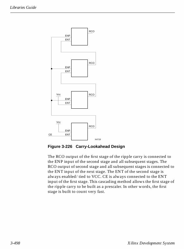
Libraries Guide
Figure 3-226 Carry-Lookahead Design
The RCO output of the first stage of the ripple carry is connected tothe ENP input of the second stage and all subsequent stages. TheRCO output of second stage and all subsequent stages is connected tothe ENT input of the next stage. The ENT of the second stage isalways enabled/tied to VCC. CE is always connected to the ENTinput of the first stage. This cascading method allows the first stage ofthe ripple carry to be built as a prescaler. In other words, the firststage is built to count very fast.
X4719
ENT
ENP
RCO
ENT
ENP
RCO
ENT
ENP
RCOVcc
Vcc
ENTCE
ENP
RCO
3-498 Xilinx Development System

Design Elements
Figure 3-227 X74_168 XC2000/3000/4000 Implementation
QD
D
UPC
XOR2
UC1
QC
QA
QB
AND2
U_DLOAD
CK
ENTCE
B
A
DB1
D0D1 OS0
M2_1DNC
XOR2
CC
DC3
DC2
OR3
UD2
AND4B1OR2
UPD
DC
Q2
FDCEQD
CLRCEC
D0D1 OS0
M2_1
UPB
UB4
UB2
AND3B2
RCO
NAND4B2
URC
OR2B2ENT_POR2
ENP
D0D1 OS0
M2_1
OR2
RC
DRC
DC1
DD1
AND4B4
D0D1 OS0
M2_1
OR4AND3B1
DD4
DD3
DD2
UB1
DB4
DB3
DB2
AND4B2
AND3B1
UDD
UDC
D0D1 OS0
M2_1
OR4
AND4B3
AND3B2
Q1
FDCEQD
CLRCEC
Q0
FDCEQD
CLRCEC
D0D1 OS0
M2_1
D0D1 OS0
M2_1
D0D1 OS0
M2_1
Q3
FDCEQD
CLRCEC
DA
DD
GND
UDAINV
AND2B1
AND2
DND
UD1
OR4
DB
UDBDNB
AND2
AND2
OR3
AND2B1
AND3
AND4B3
AND4B3
C
Libraries Guide 3-499

Libraries Guide
X74_174
6-Bit Data Register with Active-Low AsynchronousClear
The active-Low asynchronous clear input (CLR), when Low, over-rides the clock and resets the six data outputs (Q6 – Q1) Low. WhenCLR is High, the data on the six data inputs (D6 – D1) is transferred tothe corresponding data outputs on the Low-to-High clock (C) transi-tion.
dn = state of referenced input one set-up time prior to active clock transition
XC2000 XC3000 XC4000 XC7000
Macro Macro Macro Primitive
Inputs Outputs
CLR D6 – D1 CK Q6 – Q1
0 X X 01 D6 – D1 ↑ d6 – d1
X4193
X74_174
CK
D6
D5
D4
D3D2
Q3
Q2
Q1D1
Q4
Q6
Q5
CLR
3-500 Xilinx Development System
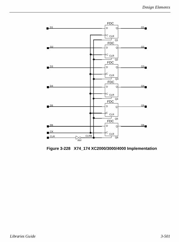
Design Elements
Figure 3-228 X74_174 XC2000/3000/4000 Implementation
CLR
CK
INV
Q5
Q4
Q3
Q2
Q1
Q6
D1
D2
D4
D3
D6
D5
CLRBQ6
QD
CLRC
FDCQ5
QD
CLRC
FDCQ4
QD
CLRC
FDCQ3
QD
CLRC
FDCQ2
QD
CLRC
FDCQ1
QD
CLRC
FDC
Libraries Guide 3-501

Libraries Guide
X74_194
4-Bit Loadable Bidirectional Serial/Parallel-InParallel-Out Shift Register
X74_194 is a 4-bit shift register with shift-right serial input (SRI), shift-left serial input (SLI), parallel inputs (D – A), parallel outputs(QD – QA), two control inputs (S1, S0), and active-Low asynchronousclear (CLR). The shift register performs the following functions.
● Clear When CLR is Low, all other inputs are ignored andoutputs QD – QA go to logic state zero during theLow-to-High clock transition.
● Load When S1 and S0 are High, the data on inputs D – Ais loaded into the corresponding output bitsQD – QA during the Low-to-High clock transition.
● Shift Right When S1 is Low and S0 is High, the data is shiftedto the next-highest bit position (right) as new datais loaded into QA (SRI➝QA, QA➝QB, QB➝QC,and so forth).
● Shift Left When S1 is High and S0 is Low, the data is shiftedto the next-lowest bit position (left) as new data isloaded into QD (SLI➝QD, QD➝QC, QC➝QB, andso forth).
Registers can be cascaded by connecting the QD output of one stageto the SRI input of the next stage, the QA output of one stage to theSRI input of the next stage, and connecting clock, S1, S0, and CLRinputs in parallel.
XC2000 XC3000 XC4000 XC7000
Macro Macro Macro Primitive
X4181
X74_194
CK
S1
S0
SRI
D
C
B
ASLI
QD
QC
QB
QA
CLR
3-502 Xilinx Development System
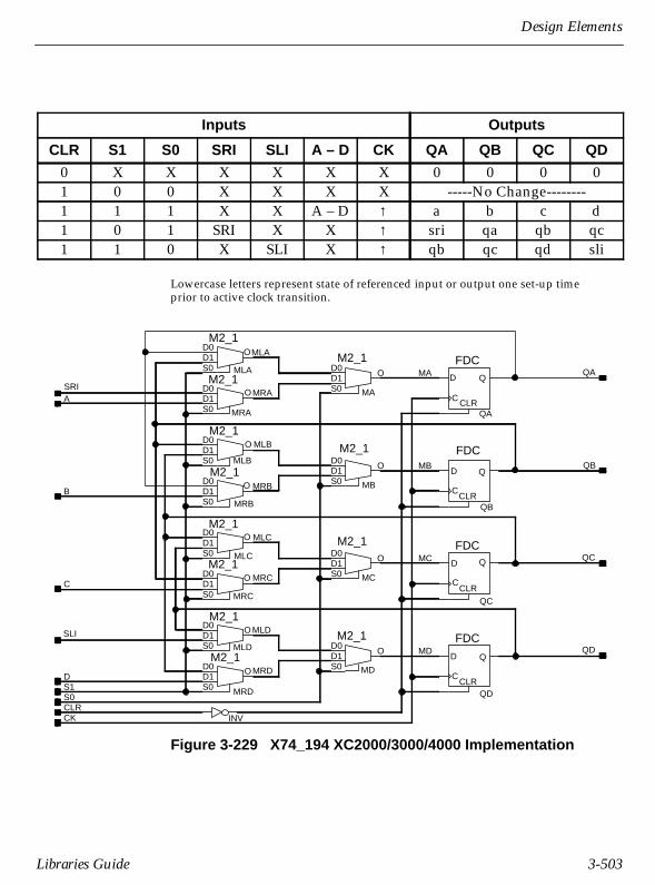
Design Elements
Lowercase letters represent state of referenced input or output one set-up timeprior to active clock transition.
Figure 3-229 X74_194 XC2000/3000/4000 Implementation
Inputs Outputs
CLR S1 S0 SRI SLI A – D CK QA QB QC QD
0 X X X X X X 0 0 0 01 0 0 X X X X -----No Change--------1 1 1 X X A – D ↑ a b c d1 0 1 SRI X X ↑ sri qa qb qc1 1 0 X SLI X ↑ qb qc qd sli
MD
D0D1
O
S0
M2_1
MA
D0D1
O
S0
M2_1
MC
D0D1
O
S0
M2_1
MB
D0D1 O
S0
M2_1
INV
MRD
D0D1
O
S0
M2_1MLD
D0D1
O
S0
M2_1
MLB
D0D1
O
S0
M2_1
MLA
D0D1
O
S0
M2_1
MRC
D0D1
O
S0
M2_1MLC
D0D1
O
S0
M2_1
MRB
D0D1
O
S0
M2_1
MRA
D0D1
O
S0
M2_1QA
QC
QB
MD
MC
MB
MA
MLD
MRD
MRB
MLA
MLB
MRC
MLC
MRA
QD
SRIA
B
C
CK
S0CLR
S1D
SLI
QD
QD
CLRC
FDC
QC
QD
CLRC
FDC
QB
QD
CLRC
FDC
QA
QD
CLRC
FDC
Libraries Guide 3-503

Libraries Guide
X74_195
4-Bit Loadable Serial/Parallel-In Parallel-Out ShiftRegister
X74_195 is a 4-bit shift register with shift-right serial inputs (J and K),parallel inputs (D – A), parallel outputs (QD – QA) and QDB,shift/load control input (S_L), and active-Low asynchronous clear(CLR). Asynchronous CLR, when Low, overrides all other inputs andresets data outputs QD – QA Low and QDB High. When S_L is Lowand CLR is High, data on the D – A inputs is loaded into the corre-sponding QD – QA bits of the register during the Low-to-High clock(C) transition. When S_L and CLR are High, the first bit of the register(QA) responds to the J and K inputs during the Low-to-High clocktransition, as shown in the truth table. During subsequent Low-to-High clock transitions, with S_L and CLR High, the data is shifted tothe next-highest bit position (shift right) as new data is loaded intoQA (J, K➝QA, QA➝QB, QB➝QC, and so forth).
Registers can be cascaded by connecting the QD and QDB outputs ofone stage to the J and K inputs, respectively, of the next stage andconnecting clock, S_L and CLR inputs in parallel.
Lowercase letters represent state of referenced input or output one set-up timeprior to active clock transition.
XC2000 XC3000 XC4000 XC7000
Macro Macro Macro Primitive
Inputs Outputs
CLR S_L J K A – D CK QA QB QC QD QDB
0 X X X X X 0 0 0 0 11 0 X X A – D ↑ a b c d d1 1 0 0 X ↑ 0 qa qb qc qc1 1 1 1 X ↑ 1 qa qb qc qc1 1 0 1 X ↑ qa qa qb qc qc1 1 1 0 X ↑ qa qa qb qc qc
X4182
X74_195
QD
QC
QB
QA
CK
S_L
K
J
D
C
B
A
CLR
QDB
3-504 Xilinx Development System

Design Elements
Figure 3-230 X74_195 XC2000/3000/4000 Implementation
CKCLR
INVCLRB
QA
QD
CLRC
FDC
QB
QD
CLRC
FDC
QC
QD
CLRC
FDC
QD
QD
CLRC
FDC
S_L
QB
QC
NAND2
NAND3B1
QD
INV
MB
D0D1
O
S0
M2_1
MC
D0D1 OS0
M2_1
MD
D0D1 OS0
M2_1
MA
D0D1 O
S0
M2_1
NAND3OR3B1
J
K
JK
D
B
A
MD
MB
MA QA
CMC
QDB
Libraries Guide 3-505
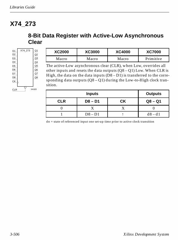
Libraries Guide
X74_273
8-Bit Data Register with Active-Low AsynchronousClear
The active-Low asynchronous clear (CLR), when Low, overrides allother inputs and resets the data outputs (Q8 – Q1) Low. When CLR isHigh, the data on the data inputs (D8 – D1) is transferred to the corre-sponding data outputs (Q8 – Q1) during the Low-to-High clock tran-sition.
dn = state of referenced input one set-up time prior to active clock transition
XC2000 XC3000 XC4000 XC7000
Macro Macro Macro Primitive
Inputs Outputs
CLR D8 – D1 CK Q8 – Q1
0 X X 01 D8 – D1 ↑ d8 – d1
X4183
X74_273
Q4
Q3
Q2
Q1
CK
D8
D7
D6
D5
D4
D3
D2
CLR
D1
Q8
Q7
Q6
Q5
3-506 Xilinx Development System

Design Elements
Figure 3-231 X74_273 XC2000/3000/4000 Implementation
CK
D8
D1
D2
D4
D3
D5
D6
D7
CLRB
Q1
Q2
Q3
Q4
Q5
Q6
Q7
Q8
INV
CLRQ8
QD
CLRC
FDCQ7
QD
CLRC
FDC Q6
QD
CLRC
FDC Q5
QD
CLRC
FDCQ4
QD
CLRC
FDCQ3
QD
CLRC
FDCQ2
QD
CLRC
FDC Q1
QD
CLRC
FDC
Libraries Guide 3-507

Libraries Guide
X74_280
9-Bit Odd/Even Parity Generator/Checker
* not supported for XC7336 designs
X74_280 parity generator/checker compares up to nine data inputs(I – A) and provides both even (EVEN) and odd parity (ODD)outputs. The EVEN output is High when an even number of inputs isHigh. The ODD output is High when an odd number of inputs isHigh.
Expansion to larger word sizes is accomplished by tying the ODDoutputs of up to nine parallel components to the data inputs of onemore X74_280; all other inputs are tied to ground.
Figure 3-232 X74_280 XC2000/3000/4000 Implementation
XC2000 XC3000 XC4000 XC7000
Macro Macro Macro Primitive*
Inputs Outputs
Number of Oneson A – I
EVEN ODD
0, 2, 4, 6, or 8 1 01, 3, 5, 7, or 9 0 1
X4184
X74_280
I
H
G
F
E
D
C
BA
ODD
EVEN
XOR5
XOR4 XNOR2
XOR2
I
HGF
EDCBA
X4
X5
EVEN
ODD
3-508 Xilinx Development System

Design Elements
X74_283
4-Bit Full Adder with Carry-In and Carry-Out
* not supported for XC7336 designs
X74_283, a 4-bit full adder with carry-in and carry-out, adds two 4-bitwords (A4 – A1 and B4 – B1) and a carry-in (C0) and produces abinary sum output (S4 – S1) and a carry-out (C4).
16(C4)+8(S4)+4(S3)+2(S2)+S1=8(A4+B4)+4(A3+B3)+2(A2+B2)+(A1+B1)+CO, where “+” = addition.
XC2000 XC3000 XC4000 XC7000
Macro Macro Macro Primitive*
X4185
X74_283
B4
B3
B2
B1
A4
A3
A2
A1CO
C4
S4
S3
S2S1
Libraries Guide 3-509

Libraries Guide
Figure 3-233 X74_283 XC2000/3000/4000 Implementation
OR3
AND2
AND2
AND2
XOR3
XOR3
OR3
AND2
AND2
AND2
AND2
AND2
AND2
AND2
AND2
AND2
OR3
XOR3
XOR3
OR3
A1
A4
A3
A2
C0
B4
B3
B2
B1
C1
C2
C3
S2
C4
S1
S3
S4
3-510 Xilinx Development System

Design Elements
X74_298
Quadruple 2-Input Multiplexer with Storage andNegative-Edge Clock
* not supported for XC7336 designs
X74_298 selects 4-bits of data from two sources (D1 – A1 or D2 – A2)under the control of a common word select input (WS). When WS isLow, D1 – A1 is chosen, and when WS is High, D2 – A2 is chosen. Theselected data is transferred into the output register (QD – QA) duringthe High-to-Low transition of the negative-edge triggered clock (CK).For XC7000, the CK input cannot be driven by a FastCLK signal(from BUFG).
an – dn = state of referenced input one set-up time prior to active clock transition
XC2000 XC3000 XC4000 XC7000
Macro Macro Macro Primitive*
Inputs Outputs
WS A1 – D1 A2 – D2 CK QA – QD
0 A1 – D1 X ↓ a1 – d11 X A2 – D2 ↓ a2 – d2
X4186
X74_298
CK
WS
D2
D1
C2
C1
B2
B1
A2
A1
QD
QC
QB
QA
Libraries Guide 3-511

Libraries Guide
Figure 3-234 X74_298 XC2000/3000/4000 Implementation
CK
QA
C
D Q
FD_1
QB
C
D Q
FD_1
QC
C
D Q
FD_1
QD
C
D Q
FD_1
D2D1
C2C1
B2B1
A2
QCMC
MD
MB
MA
QD
WS
QA
QB
A1
MD
D0D1
O
S0
M2_1
MC
D0D1
O
S0
M2_1
MB
D0D1
O
S0
M2_1
MA
D0D1
O
S0
M2_1
3-512 Xilinx Development System

Design Elements
X74_352
Dual 4-to-1 Multiplexer with Active-Low Enables andOutputs
X74_352 comprises two 4-to-1 multiplexers with separate enables(G1 and G2) but with common select inputs (A and B). When anactive-Low enable (G1 or G2) is Low, the multiplexer chooses onedata bit from the four sources associated with the particular enable(I1C3 – I1C0 for G1 and I2C3 – I2C0 for G2) under the control of thecommon select inputs (A and B). The active-Low outputs (Y1 and Y2)reflect the inverse of the selected data as shown in truth table. Y1 isassociated with G1 and Y2 is associated with G2. When an active-Low enable is High, the associated output is High.
XC2000 XC3000 XC4000 XC7000
Macro Macro Macro Primitive
Inputs Outputs
G B A IC0 IC1 IC2 IC3 Y
1 X X X X X X 10 0 0 IC0 X X X IC00 0 1 X IC1 X X IC10 1 0 X X IC2 X IC20 1 1 X X X IC3 IC3
X4187
X74_352
I1C3
I1C2
I1C1
I2C3
I2C2
I2C1
I2C0
G1
B
A
Y2
I1C0
G2
Y1
Libraries Guide 3-513
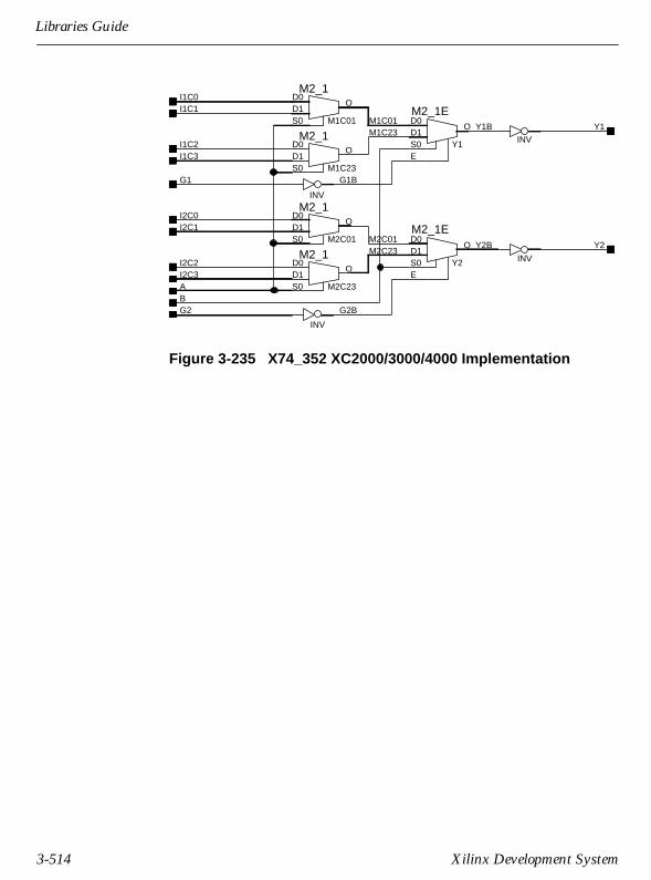
Libraries Guide
Figure 3-235 X74_352 XC2000/3000/4000 Implementation
M2C23
D0D1
O
S0
M2_1
M1C23
D0D1
O
S0
M2_1
B
M1C01
A
M2C01
D0D1
O
S0
M2_1
G1
INV
G1B
Y1
INV
Y1B
I1C2
I1C0
I1C3Y1
D1D0
O
ES0
M2_1E
M1C23
I1C1
INV
G2B
M2C01
I2C2M2C23
Y2D1D0
O
ES0
M2_1EI2C0I2C1
I2C3
Y2B
INV
Y2
G2
M1C01
D0D1
O
S0
M2_1
3-514 Xilinx Development System

Design Elements
X74_377
8-Bit Data Register with Active-Low Clock Enable
When the active-Low clock enable (G) is Low, the data on the eightdata inputs (D8 – D1) is transferred to the corresponding dataoutputs (Q8 – Q1) during the Low-to-High clock (CK) transition. Theregister ignores clock transitions when G is High.
dn = state of referenced input one set-up time prior to active clock transition
XC2000 XC3000 XC4000 XC7000
Macro Macro Macro Primitive
Inputs Outputs
G D8 – D1 CK Q8 – Q1
1 X X No Change0 D8 – D1 ↑ d8 – d1
X4188
X74_377
CK
G
D8
D7
D6
D5
D4
D3
D2
D1
Q7
Q5
Q3
Q1
Q6
Q4
Q2
Q8
Libraries Guide 3-515

Libraries Guide
Figure 3-236 X74_377 XC2000/3000/4000 Implementation
GND
INV
G
Q1D1
Q2D2
D3 Q3
D4 Q4
D5 Q5
D6 Q6
Q7D7
Q8D8
GB
CK
Q1
FDCE
QD
CLR
CE
C
Q2
FDCEQD
CLR
CE
C
Q3
FDCE
QD
CLR
CE
C
Q4
FDCEQD
CLR
CE
C
Q5
FDCEQD
CLR
CE
C
Q6
FDCE
QD
CLR
CE
C
Q7
FDCE
QD
CLR
CE
C
Q8
FDCE
QD
CLR
CE
C
3-516 Xilinx Development System

Design Elements
X74_390
4-Bit BCD/Bi-Quinary Ripple Counter withNegative-Edge Clocks and Asynchronous Clear
* not supported for XC7336 designs
X74_390 is a cascadable, resettable binary-coded decimal (BCD) orbi-quinary counter that can be used to implement cycle lengths equalto whole and/or cumulative multiples of 2 and/or 5. In BCD mode,the output QA is connected to negative-edge clock input (CKB), anddata outputs (QD – QA) increment during the High-to-Low clocktransition as shown in the truth table, provided asynchronous clear(CLR) is Low. In bi-quinary mode, output QD is connected to thenegative-edge clock input (CKA). As shown in the truth table, in bi-quinary mode, QA supplies a divide-by-five output and QB suppliesa divide-by-two output, provided asynchronous CLR is Low. Whenasynchronous CLR is High, the other inputs are overridden, and dataoutputs (QD – QA) are reset Low.
Larger ripple counters are created by connecting the QD output (BCDmode) or QA output (biquinary mode) of the first stage to the appro-priate clock input of the next stage and connecting the CLR inputs inparallel. For XC7000, CKA and CKB cannot be driven by a FastCLKsignal from (BUFG).
XC2000 XC3000 XC4000 XC7000
Macro Macro Macro Primitive*
X4189
X74_390
CLR
QC
QB
QACKA
QD
CKB
Libraries Guide 3-517

Libraries Guide
Figure 3-237 X74_390 XC2000/3000/4000 Implementation
CountBCD Bi-Quinary
QD QC QB QA QD QC QB QA
0 0 0 0 0 0 0 0 01 0 0 0 1 0 0 1 02 0 0 1 0 0 1 0 03 0 0 1 1 0 1 1 04 0 1 0 0 1 0 0 05 0 1 0 1 0 0 0 16 0 1 1 0 0 0 1 17 0 1 1 1 0 1 0 18 1 0 0 0 0 1 1 19 1 0 0 1 1 0 0 1
QD
QD
CE
CLR
Q
C
D
FDCE_1
QC
CE
CLR
Q
C
D
FDCE_1
QB
CE
CLR
Q
C
D
FDCE_1
QA
CE
CLR
Q
C
D
FDCE_1VCC
AND2B1
AND2
INV
OR2
XOR2
XOR2
NOR2
QC
QB
QA
A21
CKA
CKB
CLR
D0
AX2D2
OX3D3
D1
3-518 Xilinx Development System
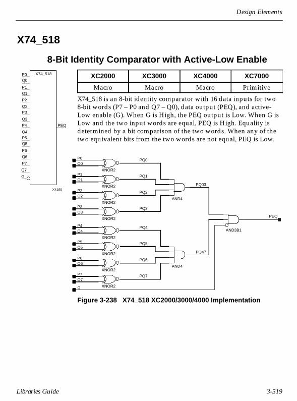
Design Elements
X74_518
8-Bit Identity Comparator with Active-Low Enable
X74_518 is an 8-bit identity comparator with 16 data inputs for two8-bit words (P7 – P0 and Q7 – Q0), data output (PEQ), and active-Low enable (G). When G is High, the PEQ output is Low. When G isLow and the two input words are equal, PEQ is High. Equality isdetermined by a bit comparison of the two words. When any of thetwo equivalent bits from the two words are not equal, PEQ is Low.
Figure 3-238 X74_518 XC2000/3000/4000 Implementation
XC2000 XC3000 XC4000 XC7000
Macro Macro Macro Primitive
X4190
X74_518
Q0
Q1
P1
P2
Q7
G
P0
P3
P4
Q3
Q4
Q2
Q5
Q6
P6
P7
P5
PEQ
G
PQ47
PQ03
AND3B1
PEQ
AND4
XNOR2
XNOR2
XNOR2
XNOR2
XNOR2
XNOR2
XNOR2
XNOR2
Q5
AND4
P0
P1
P2
P3
P4
P5
P6
P7
Q0
Q1
Q2
Q3
Q4
Q6
Q7
PQ2
PQ0
PQ6
PQ5
PQ1
PQ3
PQ7
PQ4
Libraries Guide 3-519
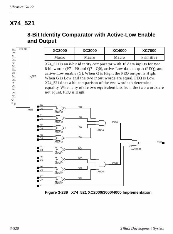
Libraries Guide
X74_521
8-Bit Identity Comparator with Active-Low Enableand Output
X74_521 is an 8-bit identity comparator with 16 data inputs for two8-bit words (P7 – P0 and Q7 – Q0), active-Low data output (PEQ), andactive-Low enable (G). When G is High, the PEQ output is High.When G is Low and the two input words are equal, PEQ is Low.X74_521 does a bit comparison of the two words to determineequality. When any of the two equivalent bits from the two words arenot equal, PEQ is High.
Figure 3-239 X74_521 XC2000/3000/4000 Implementation
XC2000 XC3000 XC4000 XC7000
Macro Macro Macro Primitive
X4191
X74_521
Q0
Q1
P1
P2
Q7
G
P0
P3
P4
Q3
Q4
Q2
Q5
Q6
P6
P7
P5
PEQ
XNOR2
XNOR2
P5
PQ4 NAND3B1
G
PQ47
PQ03
PEQ
AND4
XNOR2
XNOR2
XNOR2
XNOR2
XNOR2
XNOR2
Q5
AND4
P0
P1
P2
P3
P4
P6
P7
Q0
Q1
Q2
Q3
Q4
Q6
Q7
PQ2
PQ0
PQ6
PQ5
PQ1
PQ3
PQ7
3-520 Xilinx Development System

Chapter 4
XACT Libraries Guide — 0401410 01 4-1
Attributes, Constraints, and Carry LogicThis chapter lists and describes all the attributes and constraints thatyou can use with your schematic entry software or enter in aconstraints file. In particular, it describes the relative location (RLOC)constraint. It also describes PPR placement constraints, relationallyplaced macros (RPMs), and carry logic.
Attributes are instructions placed on symbols or nets in an FPGA orEPLD schematic to indicate their placement, implementation,naming, directionality, and so forth. This information is used by thedesign implementation software during placement and routing of adesign. Constraints, which are a type, or subset, of attributes, areused only to indicate where an element should be placed.
All the attributes listed in this chapter are available in the schematicentry tools directly supported by Xilinx unless otherwise noted, butsome may not be available in textual entry methods such as VHDL.
Attributes applicable only to a certain schematic entry tool aredescribed in the documentation for that tool. For third-party inter-faces, consult the interface user guides for information on whichattributes are available and how they are used.
AttributesThere are three types of attributes discussed in this section:
● Component attributes, which affect only the component instanceson which they are placed.
● Global attributes, which affect the entire design. These attributesapply to EPLD devices only.
● Net attributes, which affect individual component outputs orinputs and are represented by attributes applied to nets.

Libraries Guide
In some software programs, particularly Mentor Graphic’s, attributesare called properties, but their functionality is the same as that ofattributes. In this document, they are referred to as attributes.
There are two types of Mentor Graphics properties: in one, a propertyis equal to a value, for example, LOC=AA; in the other, the propertyname and the value are the same, for example, DECODE. In the firsttype, “attribute” refers to the property; in the second, “attribute”refers to the property and the value.
The attributes in this section are listed in alphabetical order.
BASE
ArchitecturesThe BASE attribute applies to the XC2000 and XC3000 families only.
DescriptionThe BASE attribute defines the base configuration of a CLB or an IOB.For an IOB primitive, it should always be set to IO. For a CLB primi-tive, it can be one of three modes in which the CLB function generatoroperates.
In XC2000 devices, these three modes are the following:
● F mode allows any function of up to four variables to be imple-mented, where one of the inputs can be the Q output of the flip-flop in the CLB.
● FG mode allows two three-input functions to be implemented,where the input can be chosen from the four inputs to the CLB andthe Q output of the flip-flop in the CLB.
● FGM mode is similar to FG mode except that the inputs must bechosen from four inputs to the CLB or the Q feedback. The B inputto the CLB acts as the control for a multiplexer between the twofour-input functions.
The three modes are very similar in XC3000 devices:
● F mode allows the CLB to implement any one function of up tofive variables.
● FG mode gives the CLB any two functions of up to four variables.
4-2 Xilinx Development System

Attributes, Constraints, and Carry Logic
Of the two sets of four variables, one input (A) must be common,two (B and C) can be either independent inputs or feedback fromthe Qx and Qy outputs of the flip-flops within the CLB, and thefourth can be either of the two other inputs to the CLB (D and E).
● FGM mode is similar to FG, but the fourth input must be the Dinput. The E input is then used to control a multiplexer betweenthe two four-input functions, allowing some six- and seven-inputfunctions to be implemented.
The following two figures illustrate the CLB and IOB base configura-tions of the XC2000 and XC3000 families, respectively. In these draw-ings, BASE F, FG, and FGM are for CLBs; BASE IO is for IOBs.
Figure 4-1 Base Configurations for XC3000 CLB and IOBPrimitives
X4708
QX
QY
F
CLB: BASE F
QX
QY
CLB: BASE FG
F
G
QX
QY
F
CLB: BASE FGM IOB: BASE IO
G
PAD
M
E
Libraries Guide 4-3

Libraries Guide
Figure 4-2 Base Configurations for XC2000 CLB and IOBPrimitives
SyntaxThe syntax of the BASE attribute is the following:
BASE=mode
where mode can be F, FG, or FGM for a CLB, or IO for an IOB.
BLKNM
Architectures The BLKNM attribute applies to all FPGA families.
DescriptionThe BLKNM attribute assigns LCA block names to qualifying primi-tives and logic elements. If the same BLKNM attribute is assigned tomore than one instance, the software attempts to map them into thesame LCA block. Conversely, two symbols with different BLKNM
X4707
QF
CLB: BASE F
Q
CLB: BASE FG
F
G
QF
CLB: BASE FGM IOB: BASE IO
G
PAD
B
M
4-4 Xilinx Development System

Attributes, Constraints, and Carry Logic
names are not mapped into the same block. Placing similar BLKNMson instances that do not fit within one LCA block creates an error.
Specifying identical BLKNM attributes on FMAP and/or HMAPsymbols tells the software to group the associated function genera-tors into a single CLB. Using BLKNM, you can partition a completeCLB without constraining the CLB to a physical location on thedevice.
For an XC4000 CLB, the maximum number of elements that can beassigned the same block name is two flip-flops, two FMAPs, and oneHMAP. For an XC3000 CLB, the maximum number of elements thatcan be assigned the same block name is two flip-flops or oneCLBMAP. For an XC2000 CLB, the maximum number is one flip-flopor one CLBMAP.
BLKNM attributes, like LOC constraints, are specified from the sche-matic. Hierarchical paths are not prefixed to BLKNM attributes, soBLKNM attributes for different CLBs must be unique throughout theentire design. See the section on the HBLKNM attribute for informa-tion on attaching hierarchy to block names.
Use the BLKNM attribute to attach a name to the following symbols:
● XC4000 flip-flop primitives (FDCE, FDPE)
● XC3000 flip-flop primitives (FDCE)
● XC2000 flip-flop and latch primitives (FDCP, LDCP)
● I/O buffers, flip-flops, and latches (IBUF, OBUF, OBUFT, ILD,IFD, OFD, OFDT)
● PAD primitives (PAD, IPAD, OPAD, BPAD, UPAD, PADU)
● I/O block primitives (IOB symbols)
● Configurable logic blocks (CLB symbols)
● 3-state buffers (BUFT symbols)
● Mapping control symbols (CLBMAP, FMAP, HMAP)
Libraries Guide 4-5
Libraries Guide
SyntaxThe syntax of the BLKNM attribute is the following:
BLKNM=blockname
where blockname is a valid LCA block name for that type of symbol.For a list of prohibited block names, see the “Naming Conventions”section of each user interface manual.
For information on assigning hierarchical block names, see theHBLKNM attribute description in this chapter.
ExampleSuppose that you want to map together two flip-flops within oneCLB. You give both the BLKNM=FFGRP1 attribute. You then trans-late, place, and route the design. When you examine it in EditLCA,you see that both flip-flops reside within a CLB named FFGRP1.
CAP
ArchitecturesThe CAP attribute applies to the XC4000H family only.
DescriptionYou can specify an XC4000H output driver as operating in eitherresistive (RES) or capacitive, “softedge” (CAP) mode. In resistivemode, the output is faster and draws more power. Use this modewhen the output is attached to purely resistive loads, or when groundbounce is not expected to be a problem with the output.
The CAP attribute allows you to specify capacitive mode. Use capaci-tive mode when connecting an output to a capacitive mode, or whenground bounce is predicted to be a problem with the output. Incapacitive mode, the pull-down transistor is slowly turned off as theoutput is pulled to ground, minimizing the likelihood of groundbounce.
See the section on the RES attribute for more information.
Use the CAP attribute on the following symbols:
4-6 Xilinx Development System
Attributes, Constraints, and Carry Logic
● IOB output symbols OBUF, OBUFT
● IOB pads OPAD, IOPAD, UPAD
● Special function access symbols TDI, TMS, TCK
SyntaxThe CAP attribute has the following syntax:
CAP
CLOCK_OPT
ArchitecturesThe CLOCK_OPT attribute applies to the XC7200 and XC7300 fami-lies only.
DescriptionThe CLOCK_OPT global attribute controls FastCLK optimization forthe entire design. FastCLK optimization changes a product-termclock to a FastCLK global signal, which reduces the number ofuniversal interconnect matrix (UIM) inputs and product termsrequired by each function block.
SyntaxUse the following syntax with the CLOCK_OPT attribute:
CLOCK_OPT={on|off}
The On setting enables FastCLK optimization; the Off setting inhibitsit. On is the default.
Libraries Guide 4-7

Libraries Guide
CMOS
ArchitecturesThe CMOS attribute applies to the XC4000H family only.
DescriptionThe CMOS attribute configures output drivers on the XC4000H todrive to CMOS-compatible levels. Similarly, it configures IOBs tohave CMOS-compatible input thresholds.
To configure output drive levels, attach the CMOS attribute to any ofthe following output symbols: OBUF, OBUFT, OUTFF/OFD,OUTFFT/OFDT.
To configure input threshold levels, attach the CMOS attribute to anyof the following input symbols: IBUF, INFF/IFD, INLAT/ILD,INREG.
See the section on the TTL attribute for more information.
SyntaxThe syntax of the CMOS attribute is the following:
CMOS
CONFIG
ArchitecturesThe CONFIG attribute applies to XC2000 and XC3000 families only.
DescriptionThe CONFIG attribute specifies logic element inputs and the storageelement function for a CLB or IOB symbol.
CONFIG attributes can only be attached to IOB and CLB symbols.
4-8 Xilinx Development System
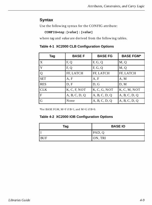
Attributes, Constraints, and Carry Logic
SyntaxUse the following syntax for the CONFIG attribute:
CONFIG=tag:[ value]:[ value]
where tag and value are derived from the following tables.
Table 4-1 XC2000 CLB Configuration Options
*For BASE FGM, M=F if B=1, and M=G if B=0.
Table 4-2 XC2000 IOB Configuration Options
Tag BASE F BASE FG BASE FGM*
X F, Q F, G, Q M, Q
Y F, Q F, G, Q M, Q
Q FF, LATCH FF, LATCH FF, LATCH
SET A, F A, F A, M
RES D, F D, G D, M
CLK K, C, F, NOT K, C, G, NOT K, C, M, NOT
F A, B, C, D, Q A, B, C, D, Q A, B, C, D, Q
G None A, B, C, D, Q A, B, C, D, Q
Tag BASE IO
I PAD, Q
BUF ON, TRI
Libraries Guide 4-9

Libraries Guide
Table 4-3 XC3000 CLB Configuration Options
*For BASE FGM, M=F if E=0, and M=G if E=1.
Table 4-4 XC3000 IOB Configuration Options
ExampleFollowing is an example of a valid XC2000 CLB CONFIG attributevalue:
X:Q Y:G CLK:K:NOT Q:FF SET:A RES:D
Here is an example of a valid XC3000 CLB CONFIG attribute value:
X:QX Y:QY DX:F DY:G CLK:K ENCLK:EC
Tag BASE F BASE FG BASE FGM*
X F, QX F, QX M, QX
Y F, QY G, QY M, QY
DX DI, F DI, F, G DI, M
DY DI, F DI, F, G DI, M
CLK K, NOT K, NOT K, NOT
RSTDIR RD RD RD
ENCLK EC EC EC
F A,B,C,D,E,QX,QY
A,B,C,D,E,QX,QY
A,B,C,D,QX,QY
G None A,B,C,D,E,QX,QY
A,B,C,D,QX,QY
Tag BASE IO
IN I, IQ, IKNOT, FF, LATCH,PULLUP
OUT O, OQ, NOT, OKNOT, FAST
TRI T, NOT
4-10 Xilinx Development System
Attributes, Constraints, and Carry Logic
DECODE
ArchitecturesThe DECODE attribute applies to the XC4000 family only.
DescriptionThe DECODE attribute defines where a wired-AND (WAND)instance is placed, either within a BUFT or an edge decoder. If theDECODE attribute is placed on a single-input WAND1 gate, the gateis implemented as an input to a wide-edge decoder in an XC4000design.
SyntaxThe syntax of the DECODE attribute is the following:
DECODE
DECODE attributes can only be attached to a WAND1 symbol.
DOUBLE
ArchitecturesThe DOUBLE attribute applies to the XC3000 family only.
DescriptionThe DOUBLE attribute specifies double pull-up resistors on the hori-zontal longline. On XC3000 parts, there are internal nets that can beset as 3-state with two programmable pull-up resistors available perline. If the DOUBLE attribute is placed on a PULLUP symbol, bothpull-ups are used, enabling a fast, high-power line. If the DOUBLEattribute is not placed on a pull-up, only one pull-up is used,resulting in a slower, lower-power line.
When the DOUBLE attribute is present, the speed of the distributedlogic is increased, as is the power consumption of the part. Whenonly half of the longline is used, there is only one pull-up at each endof the longline.
Libraries Guide 4-11

Libraries Guide
While the DOUBLE attribute can be used for the XC4000 family, it isnot recommended. PPR activates both pull-up resistors if the entirelongline (not a half-longline) is used.
SyntaxThe syntax of the DOUBLE attribute is the following:
DOUBLE
The DOUBLE attribute can only be attached to a BUFT symbol.
EQUATE_F and EQUATE_G
ArchitecturesThe EQUATE_F and EQUATE_G attributes apply to the XC2000 andXC3000 families only.
DescriptionThe EQUATE_F and EQUATE_G attributes set the logic equationsdescribing the F and G function generators of a CLB, respectively.
SyntaxThe syntax of the EQUATE_F and EQUATE_G attributes is thefollowing:
EQUATE_For EQUATE_G
The following table lists the Boolean operators used in the logic equa-tions.
Table 4-5 Valid XC2000 and XC3000 Boolean Operators
Symbol Boolean Equivalent
~ NOT
* AND
@ XOR
+ OR
( ) Group expression
4-12 Xilinx Development System

Attributes, Constraints, and Carry Logic
ExampleHere are two examples illustrating the use of the EQUATE_Fattribute:
EQUATE_F=F=((~A*B)+D))@Q
F=A@B+(C*~D)
FAST
ArchitecturesThe FAST attribute applies to XC3000, XC3000A/L, XC4000, andXC4000A families only.
DescriptionThe FAST slew-rate attribute is attached to an output buffer, outputflip-flop, or pad to increase the speed of an IOB output. It produces afaster output but may increase noise and power consumption.
The FAST attribute can be attached to the following symbols:
● IOB symbols OBUF, OBUFT, OFD, OFDI, OFDT, OFDTI, OPAD,IOPAD, UPAD
● Special function access symbols TDI, TMS, TCK
SyntaxThe syntax of the FAST attribute is the following:
FAST
FILE
ArchitecturesThe FILE attribute applies to all FPGA families.
DescriptionThe FILE attribute is placed on symbols that do not have underlyingschematics. It references the XNF file containing the Xilinx netlist for
Libraries Guide 4-13

Libraries Guide
the logic represented by the symbol. When XNFMerge encounterssuch a symbol, it looks in the design directory for the XNF file andreplaces the description of the symbol in the XNF file with the func-tionality found in the XNF file.
SyntaxUse the following syntax for the FILE attribute:
FILE= filename
where filename is the name of an XNF file without the .xnf extension.
ExampleSuppose that a symbol is created, called new_and2, whose functionmimics that of a 2-input AND gate. A Xilinx ABEL file describes thefunction of the new_and2 symbol and is translated to an XNF filecalled new_and2.xnf. A FILE attribute is placed on the symbol, andthe attribute is given a value of new_and2. The top-level designcontaining the new_and2 symbol is translated to an XNF file, and thefollowing lines are found within it:
SYM, I$2, NEW_AND2, FILE=NEW_AND2PIN, I1, I, NET_IN1PIN, I2, I, NET_IN2PIN, O1, O, NET_OUT1END
The new_and2.xnf file contains the following lines:
SYM, I$1, AND2PIN, 1, I, I1PIN, 2, I, I2PIN, O, O, O1END
4-14 Xilinx Development System
Attributes, Constraints, and Carry Logic
The top-level file is then processed by XNFMerge, which readsnew_and2.xnf and replaces the description of the symbol with thedescription of the functionality, resulting in the following lines in thetop-level design:
SYM, I$2/I$1, AND2PIN, 1, I, NET_IN1PIN, 2, I, NET_IN2PIN, O, O, NET_OUT1END
The functionality of the symbol is added to the top-level design,while the connectivity found in the top-level design is maintained.
FOE_OPT
ArchitecturesThe FOE_OPT attribute applies to the XC7200 and XC7300 familiesonly.
DescriptionThe FOE_OPT global attribute controls the optimization of the fastoutput enable (FOE) for the entire design. FOE optimization gener-ally applies only to BUFE, OBUFE, or 3-state PLD outputs driving anOBUF. FOE optimization changes a product-term 3-state signal to anFOE global control signal. Like FastCLK assignment, it reduces thenumber of UIM inputs and product terms required by each functionblock.
SyntaxUse the following syntax with the FOE_OPT attribute:
FOE_OPT={on|off}
Off inhibits FOE optimization of the entire design, and On, which isthe default, activates it.
Libraries Guide 4-15

Libraries Guide
HBLKNM
ArchitecturesThe HBLKNM attribute applies to all FPGA families.
DescriptionThe HBLKNM attribute assigns hierarchical LCA block names tologic elements and controls grouping in a flattened hierarchicaldesign. When elements on different levels of a hierarchical designcarry the same block name and the design is flattened, XNFMergeprefixes a hierarchical path name to the HBLKNM value.
Like BLKNM, the HBLKNM attribute forces function generators andflip-flops into the same CLB. Symbols with the same HBLKNMattribute map into the same CLB, if possible. However, usingHBLKNM instead of BLKNM has the advantage of adding hierarchypath names during translation, and therefore the same HBLKNMattribute and value can be used on elements within differentinstances of the same macro.
Use the HBLKNM attribute to attach a name to the followingsymbols:
● XC4000 flip-flop primitives (FDCE, FDOP)
● XC3000 flip-flop primitives (FDCE)
● XC2000 flip-flop and latch primitives (FDCP, LDCP)
● I/O buffers, flip-flops, and latches (IBUF, OBUF, OBUFT, ILD, IFD,OFD, OFDT)
● PAD primitives (PAD, IPAD, OPAD, BPAD, UPAD, PADU)
● I/O block primitives (IOB symbols)
● Configurable logic blocks (CLB symbols)
● 3-state buffers (BUFT symbols)
● Mapping control symbols (CLBMAP, FMAP, HMAP)
4-16 Xilinx Development System

Attributes, Constraints, and Carry Logic
SyntaxThe syntax of the HBLKNM attribute is the following:
HBLKNM=blockname
where blockname is a valid LCA block name for that type of symbol.For a list of prohibited block names, see the “Naming Conventions”section of each user interface manual.
ExampleA schematic is created that contains a four-input function and a flip-flop. The logic function is mapped using an FMAP symbol. Both theFMAP and the flip-flop are given the attribute HBLKNM=GROUP1.A symbol is created to represent the schematic, and both are giventhe name of FUNC. Another schematic is then created, and fourinstances of FUNC are placed on it. Because hierarchy is taken intoaccount when the design is translated, the software recognizes fourdistinct groups, as opposed to one large group called GROUP1, andeach instance of FUNC is mapped into a separate CLB.
HU_SET
ArchitecturesThe HU_SET constraint applies to the XC4000 and XC4000A/H fami-lies only.
DescriptionLike the H_SET constraint, the HU_SET constraint is defined by thedesign hierarchy. However, it also allows you to specify a set name. Itis possible to have only one H_SET constraint within a given hierar-chical element (macro) but by specifying set names, you can specifyseveral HU_SET sets.
XNFMerge hierarchically qualifies the name of the HU_SET as it flat-tens the design and attaches the hierarchical names as prefixes. Thedifference between an HU_SET constraint and an H_SET constraint isthat an HU_SET has an explicit user-defined and hierarchically quali-fied name for the set, but an H_SET constraint has only an implicithierarchically qualified name generated by the design-flatteningprogram. An HU_SET set “starts” with the symbols that are assigned
Libraries Guide 4-17

Libraries Guide
the HU_SET constraint, but an H_SET set “starts” with the instanti-ating macro one level above the symbols with the RLOC constraints.
For detailed information about this attribute, refer to the “RelativeLocation (RLOC) Constraints” section later in this chapter.
SyntaxTo designate a design element as a member of a HU_SET set, applythe following syntax to a design element:
HU_SET=name
where name is the identifier for the set; it must be unique among allthe sets in the design.
INIT
ArchitecturesThe INIT attribute applies to the XC4000 and XC4000A/H familiesonly.
DescriptionThe INIT attribute initializes ROMs.
On a ROM, the INIT attribute gives an initial value to the contents ofthe ROM. Either four or eight hexadecimal digits are required,depending on the width of the ROM.
SyntaxUse the following syntax to implement the INIT attribute:
INIT= value
For ROMs, value can be four or eight hexadecimal digits, dependingon whether the ROM is a 16- or 32-word-deep ROM, respectively.
4-18 Xilinx Development System

Attributes, Constraints, and Carry Logic
LOC
ArchitecturesThe LOC constraint applies to all families.
Description for FPGAsFor FPGAs, the LOC constraint defines where a symbol can be placedwithin an FPGA. It specifies the absolute placement of a designelement on the FPGA die. It can be a single location, a range of loca-tions, or a list of locations. The LOC constraint can only be specifiedfrom the schematic. However, statements in a constraints file can alsobe used to direct placement.
The LOC constraint can be used on the following elements:
● BUFTs
● Elements that map into a CLB: flip-flops, FMAPs, HMAPs, CLB-MAPs, CLBs
● Elements that map into an IOB: pads, IBUFs, OBUFs, INFFs, OUT-FFs, and so forth
● For XC4000 only, WANDs and clock buffers
If a LOC constraint is placed on a macro symbol, XNFMerge passes itdown onto every symbol of the appropriate type underneath thatmacro. For example, if LOC=CLB_R3C7 is placed on a macro, thatLOC constraint is passed to flip-flops and map symbols but not toBUFTs.
You can use the LOC constraint to assign a specific LCA location tothe following symbols:
● All flip-flop and latch primitives
● Xilinx soft macros (only flip-flops are affected)
● User-created symbols (only flip-flops are affected)
● Input buffers, output buffers, or pad symbols
● Clock buffers (ACLK, GCLK, BUFGP, BUFGS)
● I/O block primitives (IOB symbols) — XC2000, XC3000,XC3000A/L, XC3100, and XC3100A only
Libraries Guide 4-19

Libraries Guide
● Configurable logic blocks (CLB symbols) — XC2000, XC3000,XC3000A/L, XC3100, and XC3100A only
● 3-state buffers (BUFT symbols) — XC3000, XC3000A/L, XC3100,XC3100, and XC4000 only
● XC3000 horizontal longline pull-up resistors (PULLUP symbols)
● XC4000 wide-edge decoders (WANDn and DECODEn symbols)
● Mapping control symbols (CLBMAP, FMAP, HMAP)
You can ignore LOC constraints in the design or in various parts ofthe design by using the Ignore_xnf_locs option in XNFPrep and PPR.
You can specify multiple LOC constraints for the same symbol byusing a semicolon (;) to separate each LOC within the field. It speci-fies that the symbols be placed or prohibited from being placed in anyof the locations specified. Also, you can specify an area in which toplace a symbol or group of symbols.
The legal names are a function of the target LCA part type. However,to find the correct syntax for specifying a target location, you can loadan empty part into the XACT Design Editor (XDE). Place the cursoron any block to display its location in the lower left corner of thescreen. Do not include the pin name such as .I, .O, or .T as part of thelocation.
You can use the LOC constraint for logic that uses multiple CLBs,IOBs, soft macros, or other symbols. To do this, use the LOC attributeon a soft macro symbol, which passes the location information downto the logic on the lower level. However, the location restrictions areonly applied to the flip-flops within the logic block or to mappingsymbols or 3-state buffers in user-created macros.
Description for EPLDs For EPLDs, use the LOC=pinname attribute on a PAD symbol toassign the signal to a specific pin. The PAD symbols are IPAD, OPAD,IOPAD, and UPAD.
Pin assignments are unconditional; that is, the software does notattempt to relocate a pin if it cannot achieve the specified assignment.You can apply the LOC constraint to as many PAD symbols in yourdesign as you like. However, each pin assignment further constrains
4-20 Xilinx Development System

Attributes, Constraints, and Carry Logic
the software as it automatically allocates logic and I/O resources tointernal nodes and I/O pins with no LOC constraints.
To save all resulting pin assignments so they are preserved the nexttime you modify and re-integrate the design, use the PinSavecommand in the XDM Translate menu. This command saves the pinassignments to a design_name.vmf file. You can override individualpin assignments saved in the VMF file by changing or addingLOC=pinname attributes in the schematic.
Note: Pin assignment using the LOC attribute is not supported forbus pad symbols such as OPAD8.
Syntax for FPGAsThe syntax for specifying single LOC constraints for FPGAs is thefollowing:
LOC=location
where location is a legal LCA location for the LCA part type.
You can specify areas of CLBs or BUFTs using the LOC constraint.Specify the upper left and lower right corners of an area in whichlogic is to be placed. Use a colon (:) to separate the two boundaries.
LOC=location: location
Conversely, you can also prohibit the placement of logic into a partic-ular CLB or IOB by using the following syntax. Single locations or anentire area can be prohibited.
LOC<>location
LOC<>location: location
LOC= and LOC<> constraints can be used on the same symbol. Ifmultiple LOC= constraints are placed on a single symbol or group ofsymbols, such as a macro, they are interpreted by the software as“ORing” each of the constraints together. Multiple LOC<>constraints are interpreted as “ANDing” the constraints together. Theconvention for specifying multiple LOC constraints is to separateeach of them with a semicolon (;). Examples are shown in the “Exam-ples” section, following.
Libraries Guide 4-21

Libraries Guide
Syntax for EPLDsFor EPLDs, the LOC syntax is the following:
LOC=pinname
where the pin name is Pnn for PC packages; nn is a pin number. Thepin name is rc (row number and column number) for PG packages.Examples are LOC=P24 and LOC=G2.
ExamplesThis section gives several examples of the LOC syntax for FPGAs.
Single LOC ConstraintsExamples of the syntax for single LOC constraints are given in Table4-6.
Table 4-6 Single LOC Constraint Examples
Attribute Description
LOC=P12 Place I/O at location P12.
LOC=B Place decode logic or I/O on thebottom edge.
LOC=TL Place decode logic or I/O on thetop left edge, or global buffer in thetop left corner.
LOC=AA(XC2000 and XC3000 only)
Place logic in CLB AA.
LOC=TBUF.AC.2(XC2000 and XC3000 only)
Place BUFT in TBUF above and onecolumn to the right of CLB AC.
LOC=CLB_R3C5(XC4000 only)
Place logic in the CLB in row 3, col-umn 5.
LOC=CLB_R4C5.ffx(XC4000 only)
Place CLB flip-flop in the X flip-flopof the CLB in row 4,column 5.
LOC=CLB_R4C5.F(XC4000 only)
Place CLB function generator in theF generator of CLB-R4C5.
4-22 Xilinx Development System
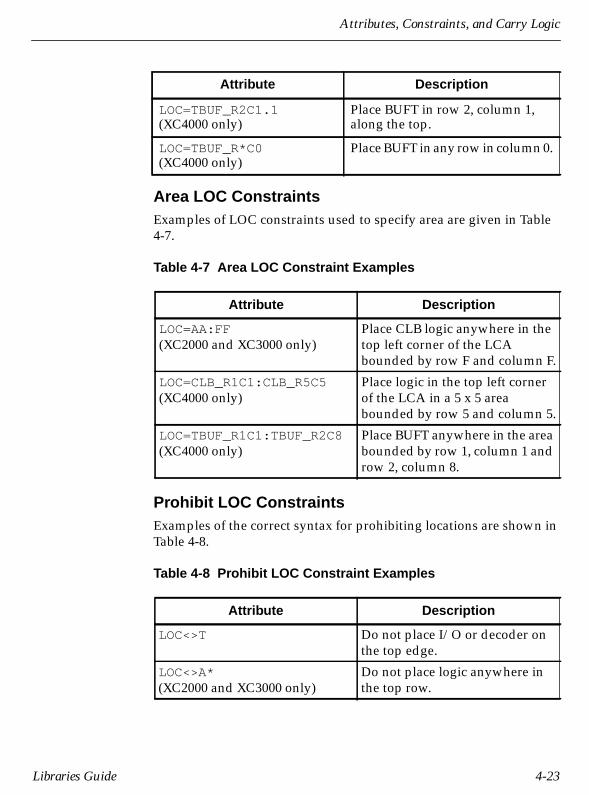
Attributes, Constraints, and Carry Logic
Area LOC ConstraintsExamples of LOC constraints used to specify area are given in Table4-7.
Table 4-7 Area LOC Constraint Examples
Prohibit LOC ConstraintsExamples of the correct syntax for prohibiting locations are shown inTable 4-8.
Table 4-8 Prohibit LOC Constraint Examples
LOC=TBUF_R2C1.1(XC4000 only)
Place BUFT in row 2, column 1,along the top.
LOC=TBUF_R*C0(XC4000 only)
Place BUFT in any row in column 0.
Attribute Description
LOC=AA:FF(XC2000 and XC3000 only)
Place CLB logic anywhere in thetop left corner of the LCAbounded by row F and column F.
LOC=CLB_R1C1:CLB_R5C5(XC4000 only)
Place logic in the top left cornerof the LCA in a 5 x 5 areabounded by row 5 and column 5.
LOC=TBUF_R1C1:TBUF_R2C8(XC4000 only)
Place BUFT anywhere in the areabounded by row 1, column 1 androw 2, column 8.
Attribute Description
LOC<>T Do not place I/O or decoder onthe top edge.
LOC<>A*(XC2000 and XC3000 only)
Do not place logic anywhere inthe top row.
Attribute Description
Libraries Guide 4-23
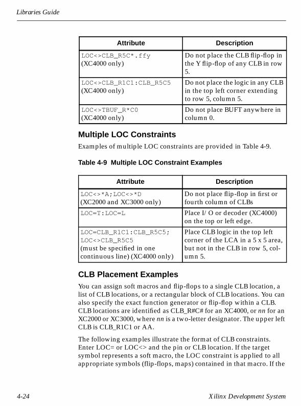
Libraries Guide
Multiple LOC ConstraintsExamples of multiple LOC constraints are provided in Table 4-9.
Table 4-9 Multiple LOC Constraint Examples
CLB Placement ExamplesYou can assign soft macros and flip-flops to a single CLB location, alist of CLB locations, or a rectangular block of CLB locations. You canalso specify the exact function generator or flip-flop within a CLB.CLB locations are identified as CLB_R#C# for an XC4000, or nn for anXC2000 or XC3000, where nn is a two-letter designator. The upper leftCLB is CLB_R1C1 or AA.
The following examples illustrate the format of CLB constraints.Enter LOC= or LOC<> and the pin or CLB location. If the targetsymbol represents a soft macro, the LOC constraint is applied to allappropriate symbols (flip-flops, maps) contained in that macro. If the
LOC<>CLB_R5C*.ffy(XC4000 only)
Do not place the CLB flip-flop inthe Y flip-flop of any CLB in row5.
LOC<>CLB_R1C1:CLB_R5C5(XC4000 only)
Do not place the logic in any CLBin the top left corner extendingto row 5, column 5.
LOC<>TBUF_R*C0(XC4000 only)
Do not place BUFT anywhere incolumn 0.
Attribute Description
LOC<>*A;LOC<>*D(XC2000 and XC3000 only)
Do not place flip-flop in first orfourth column of CLBs
LOC=T:LOC=L Place I/O or decoder (XC4000)on the top or left edge.
LOC=CLB_R1C1:CLB_R5C5;LOC<>CLB_R5C5(must be specified in onecontinuous line) (XC4000 only)
Place CLB logic in the top leftcorner of the LCA in a 5 x 5 area,but not in the CLB in row 5, col-umn 5.
Attribute Description
4-24 Xilinx Development System

Attributes, Constraints, and Carry Logic
indicated logic does not fit into the specified blocks, an error is gener-ated.
The following statements place logic in the designated CLB.
LOC=AA(XC2000 and XC3000)LOC=CLB_R1C1(XC4000)
The following statements prohibit the placement of logic in the desig-nated CLB.
LOC<>AA(XC2000 and XC3000)LOC<>CLB_R1C1(XC4000)
The following statements place logic within the first column of CLBs.The asterisk (*) is a wildcard character.
LOC=*A(XC2000 and XC3000)LOC=CLB_R*C1(XC4000)
The next two statements place logic in any of the three designatedCLBs. There is no significance to the order of the LOC statements.
LOC=AA;LOC=AB;LOC=AC(XC2000 and XC3000)LOC=CLB_R1C1;LOC=CLB_R1C2;LOC=CLB_R1C3(XC4000)
The following statements place logic within the rectangular blockdefined by the first specified CLB in the upper left corner and thesecond specified CLB in the lower right corner.
LOC=AA:HE(XC2000 and XC3000)LOC=CLB_R1C1:CLB_R8C5(XC4000)
The next statement places logic in the X flip-flop of CLB_R2C2. Forthe Y flip-flop, use the FFY tag.
LOC=CLB_R2C2.FFX(XC4000)
IOB Placement ExamplesYou can assign I/O pads, buffers, and registers to an individual IOBlocation or to a specified die edge or half-edge. IOB locations areidentified by the corresponding package pin designation or by theedge of the FPGA array.
The following examples illustrate the format of IOB constraints.Specify either LOC= or LOC<> and the pin location. If the targetsymbol represents a soft macro containing only I/O elements, for
Libraries Guide 4-25

Libraries Guide
example, INFF8, the LOC constraint is applied to all I/O elementscontained in that macro. If the indicated I/O elements do not fit intothe specified locations, an error is generated.
The following statement places the I/O element in location P13. ForPGA packages, the letter-number designation is used, for example,B3.
LOC=P13
The next statement places I/O elements in IOBs along the top edge ofthe die. For the other three die edges, use B (bottom), L (left), or R(right).
LOC=T
The following statement places I/O elements in IOBs along the tophalf of the left edge of the die. The first letter in this code representsthe die edge, and the second letter represents the desired half of thatedge. Other legal half-edge values are LB (left bottom), RT (right top),RB (right bottom), TL (top left), TR (top right), BL (bottom left), andBR (bottom right).
LOC=LT
The next statement prohibits the placement of I/O elements on theleft edge of the die.
LOC<>L
Note: The edges referred to in these constraints are die edges, whichdo not necessarily correspond to package edges. View the device inEditLCA to determine which pins are on which die edge.
BUFT Placement ExamplesYou can assign internal 3-state buffers (BUFTs) to an individual BUFTlocation, a list of BUFT locations, or a rectangular block of BUFT loca-tions. In XC4000, BUFT locations are identified by the adjacent CLB.Thus, TBUF_R1C1.1 is just above CLB_R1C1, and TBUF_R1C1.2 isjust below it in an XC4000 part. In XC2000 and XC3000, BUFT loca-tions are not as straightforward. View the device in EditLCA to deter-mine the exact BUFT names.
BUFT constraints all refer to locations with a prefix of TBUF, which isthe name of the physical element on the device.
4-26 Xilinx Development System

Attributes, Constraints, and Carry Logic
The following examples illustrate the format of BUFT LOCconstraints. Specify either LOC= or LOC<> and the BUFT location.
The following statements place the BUFT in the designated location.
LOC=TBUF.AA.1 (XC2000 and XC3000)LOC=TBUF_R1C1.1(XC4000)
The next statements place BUFTs at any location in the first column ofBUFTs. The asterisk (*) is a wildcard character.
LOC=TBUF.*A(XC2000 and XC3000)LOC=TBUF_R*C0(XC4000)
The following statements place BUFTs within the rectangular blockdefined by the first specified BUFT in the upper left corner and thesecond specified BUFT in the lower right corner.
LOC=TBUF.AA:TBUF.BH(XC2000 and XC3000)LOC=TBUF_R1C1:TBUF_R2C8(XC4000)
The following statements prohibit the placement of BUFTs at anylocation in the first row of BUFTs.
LOC<>TBUF.A*(XC2000 and XC3000)LOC<>TBUF_R1C*(XC4000)
Global Buffer Placement Examples (XC4000 Only)You can assign global buffers (BUFGP and BUFGS) to one of the fourcorners of the die. Specify either LOC= or LOC<> and the globalbuffer location. The following example illustrates the format of globalbuffer constraints.
LOC=TL
This statement places the global buffer in the top left corner of thedie. For the other three corners, use TR (top right), BL (bottom left),and BR (bottom right).
You cannot assign placement to the GCLK or ACLK buffers in theXC2000 and XC3000 families, since there is only one of each, and theirplacements are fixed on the die.
Libraries Guide 4-27

Libraries Guide
Decode Logic Placement Examples (XC4000 Only)In an XC4000 design, you can assign the decode logic to a specifieddie edge or half-edge. All elements of a single decode function mustlie along the same edge.
The following example illustrates the format of decode constraints.Specify either LOC= or LOC<> and the decode logic symbol location.If the target symbol represents a soft macro containing only decodelogic, for example, DECODE8, the LOC constraint is applied to alldecode logic contained in that macro. If the indicated decode logicdoes not fit into the specified decoders, an error is generated.
LOC=L
This statement places the decoder logic along the left edge of the die.For the other three edges, use T (top), B (bottom), or R (right).
LOGIC_OPT
ArchitecturesThe LOGIC_OPT attribute applies to the XC7200 and XC7300 familiesonly.
DescriptionThe LOGIC_OPT global attribute controls the default logic optimiza-tion for the entire design.
SyntaxThe syntax for this attribute is the following:
LOGIC_OPT={on|off}
To inhibit logic optimization for the whole design, set this attribute toOff. The default is On. You can override the global setting for indi-vidual symbols using the OPT=on or OPT=off component attribute.
4-28 Xilinx Development System
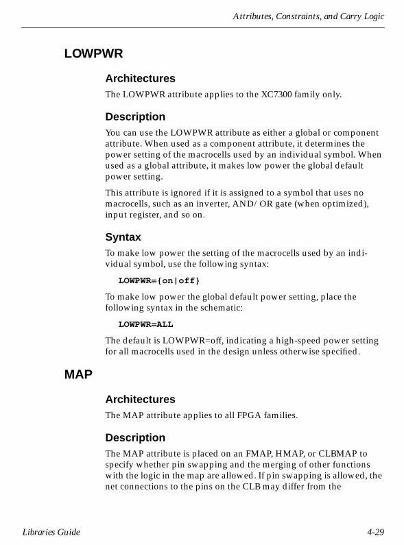
Attributes, Constraints, and Carry Logic
LOWPWR
ArchitecturesThe LOWPWR attribute applies to the XC7300 family only.
DescriptionYou can use the LOWPWR attribute as either a global or componentattribute. When used as a component attribute, it determines thepower setting of the macrocells used by an individual symbol. Whenused as a global attribute, it makes low power the global defaultpower setting.
This attribute is ignored if it is assigned to a symbol that uses nomacrocells, such as an inverter, AND/OR gate (when optimized),input register, and so on.
SyntaxTo make low power the setting of the macrocells used by an indi-vidual symbol, use the following syntax:
LOWPWR={on|off}
To make low power the global default power setting, place thefollowing syntax in the schematic:
LOWPWR=ALL
The default is LOWPWR=off, indicating a high-speed power settingfor all macrocells used in the design unless otherwise specified.
MAP
ArchitecturesThe MAP attribute applies to all FPGA families.
DescriptionThe MAP attribute is placed on an FMAP, HMAP, or CLBMAP tospecify whether pin swapping and the merging of other functionswith the logic in the map are allowed. If pin swapping is allowed, thenet connections to the pins on the CLB may differ from the
Libraries Guide 4-29
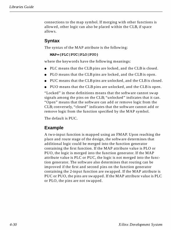
Libraries Guide
connections to the map symbol. If merging with other functions isallowed, other logic can also be placed within the CLB, if spaceallows.
SyntaxThe syntax of the MAP attribute is the following:
MAP={PLC|PUC|PLO|PUO}
where the keywords have the following meanings:
● PLC means that the CLB pins are locked, and the CLB is closed.
● PLO means that the CLB pins are locked, and the CLB is open.
● PUC means that the CLB pins are unlocked, and the CLB is closed.
● PUO means that the CLB pins are unlocked, and the CLB is open.
“Locked” in these definitions means that the software cannot swapsignals among the pins on the CLB; “unlocked” indicates that it can.“Open” means that the software can add or remove logic from theCLB; conversely, “closed” indicates that the software cannot add orremove logic from the function specified by the MAP symbol.
The default is PUC.
ExampleA two-input function is mapped using an FMAP. Upon reaching theplace and route stage of the design, the software determines thatadditional logic could be merged into the function generatorcontaining the first function. If the MAP attribute value is PLO orPUO, the logic is merged into the function generator. If the MAPattribute value is PLC or PUC, the logic is not merged into the func-tion generator. The software also determines that routing can beimproved if the first and second pins on the function generatorcontaining the 2-input function are swapped. If the MAP attribute isPUC or PUO, the pins are swapped. If the MAP attribute value is PLCor PLO, the pins are not swapped.
4-30 Xilinx Development System

Attributes, Constraints, and Carry Logic
MEDFAST and MEDSLOW
ArchitecturesThe MEDFAST and MEDSLOW attributes apply to the XC4000Afamily only.
DescriptionMEDFAST and MEDSLOW specify the slew rate of an XC4000Aoutput driver. MEDFAST decreases output transition time and isslightly faster than MEDSLOW, possibly resulting in more noise andpower consumption that an output driver specified as MEDSLOW.
The MEDFAST and MEDSLOW attributes can be attached to the I/Osymbols and the special function access symbols TDI, TMS, and TCK.
SyntaxThe syntax of the MEDFAST and MEDSLOW attributes is thefollowing:
MEDFASTor MEDSLOW
MINIMIZE
ArchitecturesThe MINIMIZE attribute applies to the XC7200 and XC7300 familiesonly.
DescriptionThe MINIMIZE global attribute determines whether or not the soft-ware minimizes the logic for the whole design. If the logic is mini-mized, any redundant or non-effective logic found in any user-speci-fied equation files is eliminated through Boolean minimization.
Libraries Guide 4-31

Libraries Guide
SyntaxThe syntax of the MINIMIZE attribute is the following:
MINIMIZE={on|off}
where On allows logic minimization, and Off inhibits it. The defaultis On.
MRINPUT
ArchitecturesThe MRINPUT attribute applies to the XC7300 family only.
DescriptionThe MRINPUT global attribute in an XC7354 or XC7336 designchanges the master reset pin to an ordinary input pin. If this attributeis set to On, the EPLD device is initialized only on power-up.
SyntaxThe syntax of the MRINPUT attribute is the following:
MRINPUT={on|off}
The On setting changes the master reset pin to an ordinary input pin.
The default is Off.
Net
ArchitecturesNet attributes apply to all families except where noted in thefollowing paragraphs.
4-32 Xilinx Development System

Attributes, Constraints, and Carry Logic
DescriptionAttaching attributes to nets affects the mapping, placement,and/or routing of the LCA design. Net attributes can be any of thefollowing values:
● C Critical (all FPGA families)
The C net attribute flags a net as critical so the software tries toroute the net earlier than others. See also W, the weight netattribute.
Note: The use of the C (critical) and W (weight net) attributes is notrecommended. In many cases, their use can degrade rather thanimprove routability and performance.
● F (XC7300 only)
The F net attribute in an XC7300 device specifies that themacrocell implementing a component output should be placed ina fast function block (FFB). When placed on the output of an IBUF,the F attribute specifies that the input signal is to use the FastInput(FI) path when the signal is used in a fast function block.
The F attribute is not valid on outputs of components that requirefeatures only present in high-density function blocks, such asPLFB9, ADD, ADSU, ACC, COMPM, LD, FDCP, FDCPE, XOR7,XOR8, and XOR9.
Note: The BUFE symbol can be assigned to FFB only when drivingan OBUF, and it must allow FOE optimization.
● G G Output (XC2000 and XC2000L only on flip-flop clock pinsand latch enable pins)
Any CLB clocks driven by this net are connected to the G functionoutput.
● H (XC7300 only)
The H net attribute in an XC7300 device specifies that themacrocell implementing a component output should be placed ina high-density function block.
The H attribute is not valid on outputs of a PLFFB9 or any of theinput/output buffer symbols.
Libraries Guide 4-33

Libraries Guide
● I C Input (XC2000 and XC2000L only on flip-flop clock pinsand latch enable pins)
Any CLB clocks driven by this net are connected to the C inputpin.
● K K Input (XC2000 and XC2000L only on flip-flop clock pinsand latch enable pins)
Any CLB clocks driven by this net are connected to the K input.
● L Longline (XC2000, XC3000, and XC3100 only)
The APR router attempts to use a longline to route this net; alongline is useful for nets with high fan-out that need low skew.
● N Non-critical (all FPGA families)
The N attribute flags a net as non-critical so the routing softwaregives this signal low priority. See also W, the weight net attribute.
Note: The use of the N (non-critical) and W (weight net) attributes isnot recommended. In many cases, their use can degrade rather thanimprove routability and performance.
● P Pin-lock (XC2000 and XC3000 only on CLBMAP primitives;XC4000 only on FMAPs and HMAPs)
The P attribute specifies that the signal should not be moved fromthe CLB pin to which it is assigned. It is useful for aligning CLBinputs with a specified longline.
● S Save (all FPGA families)
The S attribute prevents the removal of unconnected signals,which is useful when using the map-then-merge method onlower-level hierarchy. If you do not have the S attribute on a net,any signal not connected to logic and/or an I/O primitive isremoved.
● W Weight Net (all FPGA families)
The W attribute indicates the routing order of the specified net byassigning it a net weight. For XC4000 and XC3000A/L (PPR)designs, legal values are 1-99, with 0 being equivalent to the N(non-critical) attribute and 100 being equivalent to the C (critical)attribute. For XC2000 and XC3000 devices (APR), a value of 0 or 1
4-34 Xilinx Development System

Attributes, Constraints, and Carry Logic
means non-critical, 10 or higher means critical, and net weights of2 through 9 are not graded.
Note: The use of the C (critical) or N (non-critical) and W (weightnet) attributes is not recommended. In many cases, their use candegrade rather than improve routability and performance.
● X Explicit or External (all FPGA families)
With this attribute, XNFMAP or PPR ensures that a net is notmapped inside the combinational logic of a CLB, which wouldmake the net “disappear.” For example, an external net between alogic gate and a flip-flop forces the software to place thecombinational logic and the flip-flop in different CLBs. Thismapping may make the mapping of the design less efficient, but itguarantees that the flagged net exists at a CLB output, whichallows the signal to be probed in XDE.
SyntaxMethods of entering this attribute vary by user interface. Consult theappropriate user interface guide for instructions.
NODELAY
ArchitecturesThe NODELAY attribute applies to the XC4000 and XC4000A fami-lies only.
DescriptionThe default configuration of IOB flip-flops in XC4000 and XC4000Adesigns includes an input delay that results in no external hold timeon the input data path. However, this delay can be removed byplacing the NODELAY attribute on input flip-flops or latches,resulting in a smaller setup time but a positive hold time.
The NODELAY attribute can be attached to the I/O symbols and thespecial function access symbols TDI, TMS, and TCK.
Libraries Guide 4-35
Libraries Guide
SyntaxThe syntax of the NODELAY attribute is the following:
NODELAY
OPT
ArchitecturesThe OPT attribute applies to the XC7200 and XC7300 families only.
DescriptionThe OPT attribute controls the optimization of all macrocells used bya symbol.
If you build combinational logic using low-level gates and multi-plexers, the logic optimizer attempts to pack all logic boundedbetween device I/O pins and registers into a single macrocell.
The logic optimizer optimizes components forward into componentsconnected to their outputs. It also moves forward any logic, whethercombinational or sequential, that is buffered by a 3-state buffer.However, logic that itself contains a 3-state control is not movedforward.
The OPT=off attribute prevents any logic in a component from opti-mizing forward.
The OPT attribute has no effect on any symbol that contains nomacrocell logic, such as an input/output buffer.
SyntaxThe syntax of the OPT attribute is the following:
OPT={on|off}
OPT=on allows optimization of macrocell logic; OPT=off inhibitsoptimization. The default is the value of the LOGIC_OPT attribute,which is On unless otherwise specified.
4-36 Xilinx Development System

Attributes, Constraints, and Carry Logic
PLD
ArchitecturesThe PLD attribute applies to XC7200 and XC7300 families only.
DescriptionThe PLD attribute is placed on a PLD symbol to specify the name ofthe file containing the logic equations for that PLD. Use it on customprimitive symbols and the following PLDs: PL20V8, PL22V10,PL20PIN, PL24PIN, PL48PIN, PLFB9, and PLFFB9.
All PLD components in your schematic design must be assigned thePLD attribute. Running XEMake automatically assembles all equa-tion files named by all PLD=filename attributes found in the sche-matic. If you do not use XEMake, you must assemble each PLD file inthe design using PLUSASM before you run the FITNET command.
Like PLDs, user-specified (custom) primitives are defined byPLUSASM equation files. The PLD=filename attribute is not requiredbut can be applied as a convenient way to have your equation fileautomatically assembled when XEMake is invoked. If you omit thePLD attribute, FITNET will expect to find a bitmap file for the symbol(symbol_name.vmh) in your local CLIB subdirectory.
SyntaxFollowing is the syntax of the PLD attribute:
PLD=filename
Do not specify the filename extension. You must specify this filenameas the first parameter of the CHIP statement inside the equation file,as described in the “PLUSASM Language Reference” section of theXEPLD Reference Guide. Here is an example:
CHIP filename PL22V10
Libraries Guide 4-37

Libraries Guide
PRELOAD_OPT
ArchitecturesThe PRELOAD_OPT attribute applies to XC7200 and XC7300 familiesonly.
DescriptionThe PRELOAD_OPT global attribute allows the XEPLD software tochange the preload values in the design to match the preload valuessupported by specified device resources such as fast function blocksand input registers. The XEPLD software can therefore map yourdesign most efficiently, using the device resources most suited to theelements of your design. Unless you specify PRELOAD_OPT=off, thesoftware is free to change the initial register states of any component,including PLD (custom) components defined in PLUSASM. UsePRELOAD=off to preserve the initial states specified in this manualfor library components and in the PRLD equations in your PLUSASMfile for PLD or custom components.
You can set a high or low preload for high-density function blocks.The preload value of fast function blocks depends on the use of Set orReset. Input register preload values are fixed at 1, except for those onthe XC7272, which are undefined.
SyntaxThe syntax of the PRELOAD_OPT attribute is the following:
PRELOAD_OPT={on|off}
The On setting, which is the default, allows XEPLD to change thepreload values; Off preserves all preload values defined in the libraryand specified in your PLD equation files.
4-38 Xilinx Development System
Attributes, Constraints, and Carry Logic
REG_OPT
ArchitecturesThe REG_OPT attribute applies to XC7200 and XC7300 families only.
DescriptionThe REG_OPT global attribute controls input register optimizationfor the entire design. Input register optimization reduces the numberof macrocells in a design by moving simple FD registers connected toIBUFs into a pad register, provided that the IBUF has no otherfanouts. The clock by which the input register is controlled must be aFastCLK or an input that can be assigned to a FastCLK pin.
SyntaxUse the following the syntax with the REG_OPT option:
REG_OPT={on|off}
To inhibit input register optimization, set this attribute to Off. Toenable this optimization, set it to On, which is the default.
RES
ArchitecturesThe RES attribute applies to the XC4000H family only.
DescriptionYou can specify an XC4000H output driver as operating in eitherresistive (RES) or capacitive, “softedge” (CAP) mode. In resistivemode, the output is faster and draws more power. Use this modewhen the output is attached to purely resistive loads, or whenground bounce is not predicted to be a problem with the output. TheRES attribute allows you to specify resistive mode.
Libraries Guide 4-39

Libraries Guide
Use capacitive mode when connecting an output to a capacitivemode, or when ground bounce is predicted to be a problem with theoutput. In capacitive mode, the pull-down transistor is slowly turnedoff as the output is pulled to ground, minimizing the likelihood ofground bounce.
See the section on the CAP attribute for more information.
The RES attribute can be attached to the I/O symbols and the specialfunction access symbols TDI, TMS, and TCK.
SyntaxThe syntax of the RES attribute is the following:
RES
RLOC
ArchitecturesThe RLOC constraint applies to XC4000 and XC4000A/H familiesonly.
DescriptionRelative location (RLOC) constraints group logic elements intodiscrete sets and allow you to define the location of any elementwithin the set relative to other elements in the set, regardless of even-tual placement in the overall design. See the “Relative Location(RLOC) Constraints” section later in this chapter for detailed infor-mation about this type of constraint.
SyntaxUse the following syntax with the RLOC constraint:
RLOC=Rrow#Ccolumn#[. extension]
where the row and column numbers can be any positive integer,including zero.
The optional .extension can take all the values that are available withthe current absolute LOC syntax: FFX, FFY, F, G, H, 1, and 2. The 1and 2 values are available for BUFT primitives, and the rest are
4-40 Xilinx Development System

Attributes, Constraints, and Carry Logic
available for primitives associated with CLBs. Only extensions for theXC4000 family designs are currently supported.
The RLOC value cannot specify a range or a list of several locations; itmust specify a single location.
See the “Relative Location (RLOC) Constraints” section later in thischapter for information on the RLOC syntax.
RLOC_ORIGIN
ArchitecturesThe RLOC_ORIGIN constraint applies to XC4000 and XC4000A/Hfamilies only.
Description
An RLOC_ORIGIN constraint fixes the members of a set at exact dielocations. This constraint must specify a single location, not a rangeor a list of several locations. For detailed information about thisconstraint, refer to the “Relative Location (RLOC) Constraints”section later in this chapter.
The RLOC_ORIGIN constraint is required for a set that includesBUFT symbols.
SyntaxThe syntax of the RLOC_ORIGIN constraint is the following:
RLOC_ORIGIN=Rrow#Ccolumn#
where the row and column numbers are positive non-zero integers.
Libraries Guide 4-41

Libraries Guide
RLOC_RANGE
ArchitecturesThe RLOC_RANGE constraint applies to XC4000 and XC4000A/Hfamilies only.
DescriptionThe RLOC_RANGE constraint is similar to the RLOC_ORIGINconstraint except that it limits the members of a set to a certain rangeon the die. The range or list of locations is meant to apply to all appli-cable elements with RLOCs, not just to the origin of the set.
SyntaxThe RLOC_RANGE constraint has the following syntax:
RLOC_RANGE=Rrow1#Ccol#:R row2#Ccol2#
where the row numbers and the column numbers can be non-zeropositive numbers or the wildcard (*) character. This syntax allowsthree kinds of range specifications, which are defined in theRLOC_RANGE section of the “Relative Location (RLOC)Constraints” section later in this chapter.
TNM
ArchitecturesThe TNM attribute applies to XC3000A/L, XC3100A, and XC4000families only, and only when XACT-Performance is used.
DescriptionThe TNM attribute tags specific flip-flops, RAMs, pads, and inputlatches as members of a group to simplify the application of timingspecifications to the group.
See the “XACT-Performance Utility” chapter of the XACT ReferenceGuide for detailed information about this attribute.
4-42 Xilinx Development System

Attributes, Constraints, and Carry Logic
SyntaxFollowing is the syntax of the TNM attribute:
TNM=identifier
where identifier can be any combination of letters, numbers, or under-scores.
Do not use reserved words, such as FFS, LATCHES, RAMS, or PADSfor TNM identifiers.
TSidentifier
ArchitecturesThe TSidentifier attribute applies to XC3000A/L, XC3100A, andXC4000 families only.
DescriptionTSidentifier properties beginning with the letters “TS” are placed onthe TIMESPEC symbol. The value of the TSidentifier attribute corre-sponds to a specific timing specification that can then be applied topaths in the design.
See the “XACT-Performance Utility” chapter of the XACT ReferenceGuide for detailed information about this attribute.
SyntaxThe syntax of the TSidentifier attribute is the following:
TSidentifier
where identifier can be any combination of letters, numbers, or under-scores. It is commonly 01, 02, 03, and so forth. In Mentor, it must be01, 02, 03, and so forth.
Libraries Guide 4-43
Libraries Guide
TTL
ArchitecturesThe TTL attribute applies to the XC4000H family only.
DescriptionThe TTL attribute configures output drivers on the XC4000H to driveto TTL-compatible levels. Similarly, it configures IOBs to have TTL-compatible input thresholds.
To configure output drive levels, attach the TTL attribute to any of thefollowing output symbols: OBUF, OBUFT, OUTFF/OFD, OUTFFT/OFDT.
To configure input threshold levels, attach the TTL attribute to any ofthe following input symbols: IBUF, INFF/IFD, INLAT/ILD, INREG.
See the section on the CMOS attribute for more information.
SyntaxThe syntax of the TTL attribute is the following:
TTL
UIM_OPT
ArchitecturesThe UIM_OPT attribute applies to the XC7200 and XC7300 familiesonly.
DescriptionUIM optimization extracts AND expressions and inverters out ofmacrocell logic functions and moves them into the UIM, whichreduces the use of function block resources. The UIM_OPT globalattribute turns this type of optimization on or off.
4-44 Xilinx Development System

Attributes, Constraints, and Carry Logic
SyntaxThe syntax of the UIM_OPT attribute is the following:
UIM_OPT={on|off}
where On activates UIM optimization, and Off inhibits it. The Onsetting is the default.
USE_RLOC
ArchitecturesThe USE_RLOC constraint applies to the XC4000 and XC4000A/Hfamilies only.
DescriptionThe USE_RLOC constraint turns on or off the RLOC constraint for aspecific element or section of a set. For detailed information aboutthis constraint, refer to the “Relative Location (RLOC) Constraints”section later in this chapter.
SyntaxThe syntax of the USE_RLOC constraint is the following:
USE_RLOC={true|false}
where True turns on the RLOC attribute for a specific element, andFalse turns it off.
U_SET
ArchitecturesThe U_SET constraint applies to the XC4000 and XC4000A/H fami-lies only.
DescriptionThe U_SET constraint groups design elements with attached RLOCconstraints that are distributed throughout the design hierarchy intoa single set. The elements that are members of a U_SET can cross the
Libraries Guide 4-45

Libraries Guide
design hierarchy; that is, you can arbitrarily select objects withoutregard to the design hierarchy and tag them as members of a U_SET.For detailed information about this attribute, refer to the “RelativeLocation (RLOC) Constraints” section later in this chapter.
SyntaxThe syntax of the U_SET constraint is the following:
U_SET=name
where name is the identifier of the set. This name is absolute; youspecify it, and it is not prefixed by a hierarchical qualifier.
PPR Placement ConstraintsThis section describes the legal PPR placement constraints for eachtype of logic element, such as flip-flops, I/O pads, BUFTs, memories,3-state buffers, global buffers, and edge decoders in FPGA designs.Individual logic gates, such as AND or OR gates, are mapped intoCLB function generators before the constraints are read and thereforecannot be constrained. However, if gates are represented by an FMAPor HMAP symbol, you can place a placement constraint on thatsymbol.
This section first describes the syntax for using constraints on sche-matics and in a constraints (CST) file, then it gives examples showinghow both kinds of syntax are used to place constraints on the varioustypes of logic elements.
Schematic SyntaxThis section describes how to place constraints on symbols on a sche-matic. You can use LOC, RLOC, BLKNM, and HBLKNM constraintson these symbols; these constraints are described earlier in thischapter in the “Attributes” section. Although you can prohibit indi-vidual symbols from being placed in a certain location, you cannotprohibit symbol placement in general.
To specify a single location, use the following syntax:
constraint=location
4-46 Xilinx Development System
Attributes, Constraints, and Carry Logic
To specify a list of locations, use this syntax:
constraint=location; constraint=location; constraint=location...;
The following syntax defines the two corners of a bounding box:
constraint=blockname: blockname
A colon is only used to separate the corners of a bounding box.
A semicolon separates locations.
The < > arrows can be substituted for the equals sign, =, to specify a“prohibit” location constraint.
Here are some examples of location constraints:
LOC=CLB_R1C2
LOC=P12
LOC=CLB_R5C6;LOC=CLB_R6C6
LOC=CLB_R2C2:CLB_R3C3
LOC<>CLB_R1C2
LOC<>P7
Constraints File SyntaxThis section describes how to place constraints on instances andblocks in the constraints file. It also gives the syntax for all the state-ments that can be placed in the constraints file.
Instances and BlocksBecause the statements in the constraints file concern instances andblocks, these entities are defined here.
An instance is a symbol on the schematic. An instance name is thesymbol name as it appears in the XNF file. Instance constraints areused for XC4000 designs.
A block is a CLB or an IOB. A block name depends on the designfamily used. In XC3000 and XC3000A/L designs, the name isassigned by XNFMAP using BLKNM, HBLKNM, and signal names
Libraries Guide 4-47

Libraries Guide
associated with the block. In XC4000 designs, you assign the blockname with the BLKNM or HBLKNM attribute.
Place Instance ConstraintsThe Place Instance constraint instructs PPR to place or not place aninstance in a specific location.The Place Instance and NotplaceInstance constraints cannot be used for XC3000A/L or XC3100Adesigns, because the design is partitioned into CLBs before PPRprocesses it. Only the Place Block and Notplace Block statements,described in the next section, are allowed for these families, sincethese constraints operate on mapped blocks instead of mappedinstances.
The general syntax for placing PPR constraints on an instance in theconstraints file is the following:
{place|notplace} instance instance_name: location;
where the keywords are the following:
● Place Instance specifies the location of an instance to be placed.
● Notplace Instance prohibits placement of an instance in the speci-fied location.
Instance_name is the name of the instance affected by the keyword.
Location can be one of the following three types of locations:
● Single location
● List of locations separated by spaces
● Locations of two bounding box corners, which must be enclosedin square brackets and separated by spaces.
The syntax that you can use to specify locations is given in the “State-ments” section later in this chapter.
Each constraint statement must end with a semicolon(;).
A colon separates the instance name from the location in constraintstatements.
4-48 Xilinx Development System

Attributes, Constraints, and Carry Logic
Following are some examples showing how instances areconstrained:
place instance $1I2/$1I3:CLB_R5C3;
place instance $2I3/$2I5/$3I6:P12;
Place Block ConstraintsThe Place Block constraint constrains CLBs or IOBs that have beennamed by BLKNM or HBLKNM attributes, or by XNFMAP forXC3000, XC3000A/L, or XC3100A designs. The general syntax of thisconstraint is the following:
{place|notplace} block blockname: location;
where the keywords are the following:
● Place Block specifies the location of a block to be placed.
● Notplace Block prohibits placement of a block in the specifiedlocation.
For CLBs, the blockname field must match the BLKNM attribute on theindividual FMAPs, HMAPs, CLBMAPs, and/or flip-flops. For IOBs,the blockname must match the BLKNM attribute on individual I/Oelements.
The location for CLBs can be a single CLB location, a range of CLBs, ora wildcard constraint. For IOBs, the location is a package pin, such asP12 or A6, or a die edge, such as T for top. The syntax that you canuse to specify locations is given in the “Statements” section later inthis chapter. Each constraint statement must end with a semicolon(;).
A colon separates the instance name from the location in constraintstatements.
Here are some examples showing how CLBs are constrained:
place block ABC:CLB_R3C7;place block DEF:[CLB_R1C2 CLB_R5C4];place block GHI:CLB_R*C3;
The Place Block constraint differs from other PPR constraints becausethe logic is referenced by the LCA block name rather than the XNFsymbol’s instance name.
Libraries Guide 4-49

Libraries Guide
Syntactical ConventionsThe following syntactical conventions are used in the CST file state-ments given in the “Statements” section, following:
● Lower-case words are literal.
● [ 0-9] means a range of numbers between 0 and 9, inclusive.
● [ a-z] means a range of characters between A and Z, inclusive.
● ::= means “can be composed of.”
● | indicates alternatives; you must select either one or the other.
● {} means that you must choose one of the items enclosed in thebrackets.
● [] enclose items that are optional. Brackets also enclose a range.
● Items in italics are variables for which you substitute a value.
● Items in Courier , or typewriter , font are to be entered liter-ally.
WildcardsYou can use the wildcard (*) character in constraint statements asfollows.
In an instance name, a wildcard character by itself represents everysymbol of the appropriate type. For example, the following constraintapplies to every BUFT in the design:
notplace instance *: TBUF_R1C1.1;
If the wildcard character is used as part of a longer instance name, thewildcard represents one or more characters at that position. However,only symbols of the appropriate type are constrained. For example,consider the following constraint:
notplace instance cntr/q*: CLB_R7C3;
This constraint would apply to a flip-flop named cntr/q7, but not to aBUFT named cntr/q7_data.
In a location, a wildcard character can be used for either the rownumber or column number. For example, the following constraint
4-50 Xilinx Development System

Attributes, Constraints, and Carry Logic
prevents the flip-flop named cntr/q0 from being placed in any CLBin the third column:
notplace instance cntr/q0: CLB_R*C3;
Wildcard characters cannot be used in dot extensions; for example,CLB_R1C3.* is illegal.
StatementsFollowing are the statements that you can use in the CST file. It is notrecommended that you use the flag_constraint and weight_constraintstatements.
constraints ::= { place_constraint| flag_constraint| weight_constraint| time_spec| time_grp}
Place Constraintsplace_constraint ::= { place_instance| place_block}
place_instance ::= {place|notplace} instance instance_list:loc_list;
instance_list ::= alphanum [ alphanum alphanum alphanum...]
loc_list ::= loc_spec [ loc_spec loc_spec loc_spec... ]
loc_spec ::= { clb_locs| pin_locs| edge_locs| buft_locs}
clb_locs ::= { clb_loc[ bel] |[ clb_loc clb_loc][ bel]} , where [ clb_locclb_loc] is a range from the lowest to the highest.
bel ::= .{f|g|ffx|ffy|1|2}
clb_loc ::= clb_r row_col c row_col
row_col ::= number, where number can be any number between 0 and99, inclusive.
pin_locs ::= See the appropriate data book for the pin packagenames, for example, p12, or unbonded pad names, for example, u16.
edge_locs ::= {t|b|l|r|tl|tr|bl|br|rt|rb|lt|lb}
The edge locations corresponding to these terms are given in the“I/O Constraints” section later in this chapter.
Libraries Guide 4-51
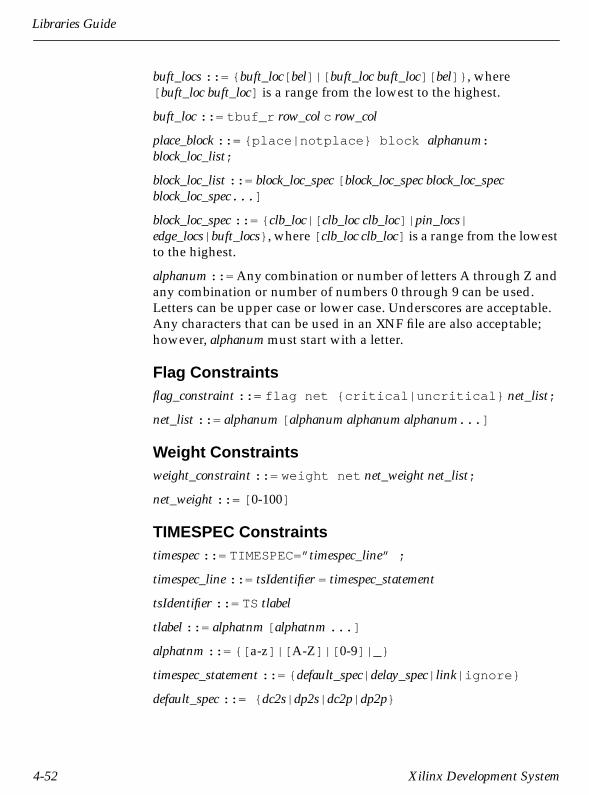
Libraries Guide
buft_locs ::= { buft_loc[ bel]|[ buft_loc buft_loc][ bel]} , where[ buft_loc buft_loc] is a range from the lowest to the highest.
buft_loc ::= tbuf_r row_col c row_col
place_block ::= {place|notplace} block alphanum:block_loc_list;
block_loc_list ::= block_loc_spec [ block_loc_spec block_loc_specblock_loc_spec... ]
block_loc_spec ::= { clb_loc|[ clb_loc clb_loc]| pin_locs|edge_locs| buft_locs} , where [ clb_loc clb_loc] is a range from the lowestto the highest.
alphanum ::= Any combination or number of letters A through Z andany combination or number of numbers 0 through 9 can be used.Letters can be upper case or lower case. Underscores are acceptable.Any characters that can be used in an XNF file are also acceptable;however, alphanum must start with a letter.
Flag Constraintsflag_constraint ::= flag net {critical|uncritical} net_list;
net_list ::= alphanum [ alphanum alphanum alphanum...]
Weight Constraintsweight_constraint ::= weight net net_weight net_list;
net_weight ::= [ 0-100]
TIMESPEC Constraintstimespec ::= TIMESPEC=” timespec_line” ;
timespec_line ::= tsIdentifier = timespec_statement
tsIdentifier ::= TS tlabel
tlabel ::= alphatnm [ alphatnm ...]
alphatnm ::= {[ a-z]|[ A-Z]|[ 0-9]|_}
timespec_statement ::= { default_spec| delay_spec| link|ignore}
default_spec ::= { dc2s| dp2s| dc2p| dp2p}
4-52 Xilinx Development System

Attributes, Constraints, and Carry Logic
delay_spec ::= { from_to| c2s| p2s| c2p| p2p}
link ::= link: tsIdentifier[: tsIdentifier: tsIdentifier...]
dc2s ::= dc2s: dmax_delay[: thi]
dp2s ::= dp2s: dmax_delay
dc2p ::= dc2p: dmax_delay
dp2p ::= dp2p: dmax_delay
from_to ::= from: group:to: group=max_delay
c2s ::= c2s: dmax_delay[: thi]
p2s ::= p2s: dmax_delay[: signame]
c2p ::= c2p: dmax_delay[: signame]
p2p ::= p2p: dmax_delay: signame: signame
dmax_delay ::= { requirement|auto|ignore}
thi ::= float_number
group ::= { tlabel| whole_class|pattern}
whole_class ::= {ffs|pads|rams|latches}
max_delay ::= { requirement|auto}
pattern ::= whole_class ( signame {: signame})
signame ::= { alphanum|*|?}[{ alphanum|*|?}...]
requirement ::= { float_number [ unit]| reference}
unit ::= {ns|us|mhz|khz}
reference ::= tsIdentifier operator float_number
operator ::= *|/ In this case, the asterisk is a multiplier, not a wild-card.
float_number ::= number [. number] , where number can be anynumber between 0 and 9, inclusive.
Libraries Guide 4-53

Libraries Guide
TIMEGRP Constraintstimegrp ::= TIMEGRP=” timegrp_line” ;
timegrp_line ::= tlabel=derived_group
derived_group ::= compound| difference| rise_fall
compound ::= group[: group : group...]
difference ::= compound:except: compound
rise_fall ::= edge: group
edge ::= {rising|falling}
RestrictionsYou should observe the following restrictions when using constraintsin the CST file.
● Use only pin_locs and edge_locs to place constraints on IOB ele-ments.
● Use only two-character edge_locs on BUFGSs and BUFGPs.
● Since BUFGs can only go in corners, “tl” means the top left corner.For IOBs, “tl” means the top left half-edge.
● Do not use Notplace Instance with decoders or WANDs having aDECODE attribute.
● BUFT_locs can only be used on BUFT elements.
● On decoders only, use full- or half-edge constraints; no pin_locs areallowed. You can only specify one location.
Determining Symbol NamesIn a constraints file, each placement constraint acts upon one or moresymbols. Every symbol in a design carries a unique name, which isdefined in the input file. Use this name in a constraint statement toidentify the symbol.
For each type of constraint described in the following sections, themethod of determining the symbol name is explained and examplesare given.
4-54 Xilinx Development System
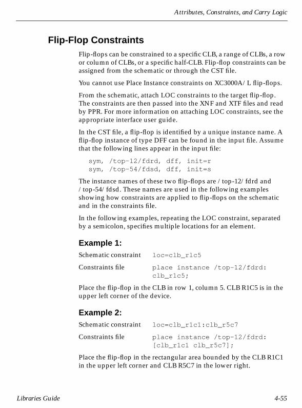
Attributes, Constraints, and Carry Logic
Flip-Flop ConstraintsFlip-flops can be constrained to a specific CLB, a range of CLBs, a rowor column of CLBs, or a specific half-CLB. Flip-flop constraints can beassigned from the schematic or through the CST file.
You cannot use Place Instance constraints on XC3000A/L flip-flops.
From the schematic, attach LOC constraints to the target flip-flop.The constraints are then passed into the XNF and XTF files and readby PPR. For more information on attaching LOC constraints, see theappropriate interface user guide.
In the CST file, a flip-flop is identified by a unique instance name. Aflip-flop instance of type DFF can be found in the input file. Assumethat the following lines appear in the input file:
sym, /top-12/fdrd, dff, init=rsym, /top-54/fdsd, dff, init=s
The instance names of these two flip-flops are /top-12/fdrd and/top-54/fdsd. These names are used in the following examplesshowing how constraints are applied to flip-flops on the schematicand in the constraints file.
In the following examples, repeating the LOC constraint, separatedby a semicolon, specifies multiple locations for an element.
Example 1:Schematic constraint loc=clb_rlc5
Constraints file place instance /top-12/fdrd:clb_r1c5;
Place the flip-flop in the CLB in row 1, column 5. CLB R1C5 is in theupper left corner of the device.
Example 2:Schematic constraint loc=clb_r1c1:clb_r5c7
Constraints file place instance /top-12/fdrd:[clb_r1c1 clb_r5c7];
Place the flip-flop in the rectangular area bounded by the CLB R1C1in the upper left corner and CLB R5C7 in the lower right.
Libraries Guide 4-55
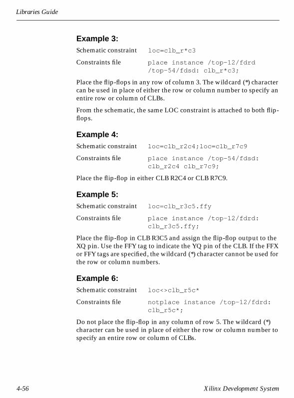
Libraries Guide
Example 3:Schematic constraint loc=clb_r*c3
Constraints file place instance /top-12/fdrd/top-54/fdsd: clb_r*c3;
Place the flip-flops in any row of column 3. The wildcard (*) charactercan be used in place of either the row or column number to specify anentire row or column of CLBs.
From the schematic, the same LOC constraint is attached to both flip-flops.
Example 4:Schematic constraint loc=clb_r2c4;loc=clb_r7c9
Constraints file place instance /top-54/fdsd:clb_r2c4 clb_r7c9;
Place the flip-flop in either CLB R2C4 or CLB R7C9.
Example 5:Schematic constraint loc=clb_r3c5.ffy
Constraints file place instance /top-12/fdrd:clb_r3c5.ffy;
Place the flip-flop in CLB R3C5 and assign the flip-flop output to theXQ pin. Use the FFY tag to indicate the YQ pin of the CLB. If the FFXor FFY tags are specified, the wildcard (*) character cannot be used forthe row or column numbers.
Example 6:Schematic constraint loc<>clb_r5c*
Constraints file notplace instance /top-12/fdrd:clb_r5c*;
Do not place the flip-flop in any column of row 5. The wildcard (*)character can be used in place of either the row or column number tospecify an entire row or column of CLBs.
4-56 Xilinx Development System
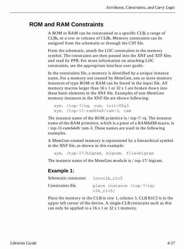
Attributes, Constraints, and Carry Logic
ROM and RAM ConstraintsA ROM or RAM can be constrained to a specific CLB, a range ofCLBs, or a row or column of CLBs. Memory constraints can beassigned from the schematic or through the CST file.
From the schematic, attach the LOC constraints to the memorysymbol. The constraints are then passed into the XNF and XTF filesand read by PPR. For more information on attaching LOCconstraints, see the appropriate interface user guide.
In the constraints file, a memory is identified by a unique instancename. For a memory not created by MemGen, one or more memoryinstances of type ROM or RAM can be found in the input file. Allmemory macros larger than 16 x 1 or 32 x 1 are broken down intothese basic elements in the XNF file. Examples of non-MemGenmemory instances in the XNF file are shown following:
sym, /top-7/rq, rom, init=05a3sym, /top-11-ram64x8/ram-3, ram
The instance name of the ROM primitive is /top-7/rq. The instancename of the RAM primitive, which is a piece of a RAM64X8 macro, is/top-11-ram64x8/ram-3. These names are used in the followingexamples.
A MemGen-created memory is represented by a hierarchical symbolin the XNF file, as shown in this example:
sym, /top-17/bigram, bigram, file=bigram
The instance name of the MemGen module is /top-17/bigram.
Example 1:Schematic constraint loc=clb_r1c5
Constraints file place instance /top-7/rq:clb_r1c5;
Place the memory in the CLB in row 1, column 5. CLB R1C5 is in theupper left corner of the device. A single-CLB constraint such as thiscan only be applied to a 16 x 1 or 32 x 1 memory.
Libraries Guide 4-57

Libraries Guide
Example 2:Schematic constraint loc=clb_r2c4;loc=clb_r7c9
Constraints file place instance /top-7/rq:clb_r2c4 clb_r7c9
Place the memory in either CLB R2C4 or CLB R7C9.
Example 3:Schematic constraint loc=clb_r1c1:clb_r5c7
Constraints file place instance /top-17/bigram/*:[clb_r1c1 clb_r5c7];
Place the MemGen module in the rectangular area bounded by theCLB R1C1 in the upper left corner and CLB R5C7 in the lower right.
From the schematic, attach the LOC constraint to the MemGensymbol.
In the CST file, the /* is appended to the end of the MemGen symbolinstance name found in the XNF file. The wildcard (*) character isused here to specify all instances that begin with the /top-17/bigram/ prefix.
Example 4:Schematic constraint loc<>clb_r5c*
Constraints file notplace instance /top11ram64x8*:clb_r5c*;
Do not place the memory in any column of row 5. The wildcard (*)character can be used in place of either the row or column number inthe CLB name to specify an entire row or column of CLBs.
From the schematic, the LOC constraint is simply attached to theRAM64X8 macro symbol and is passed through to each individualRAM in the XNF file.
In the CST file, the wildcard (*) character specifies all instances thatbegin with the /top-11-/ram64x8/ prefix.
4-58 Xilinx Development System
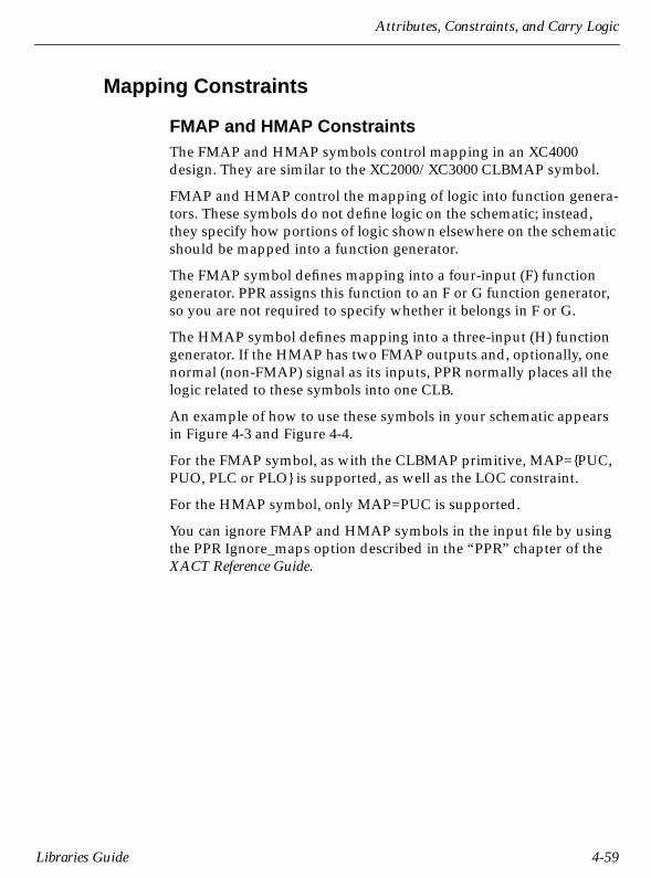
Attributes, Constraints, and Carry Logic
Mapping Constraints
FMAP and HMAP ConstraintsThe FMAP and HMAP symbols control mapping in an XC4000design. They are similar to the XC2000/XC3000 CLBMAP symbol.
FMAP and HMAP control the mapping of logic into function genera-tors. These symbols do not define logic on the schematic; instead,they specify how portions of logic shown elsewhere on the schematicshould be mapped into a function generator.
The FMAP symbol defines mapping into a four-input (F) functiongenerator. PPR assigns this function to an F or G function generator,so you are not required to specify whether it belongs in F or G.
The HMAP symbol defines mapping into a three-input (H) functiongenerator. If the HMAP has two FMAP outputs and, optionally, onenormal (non-FMAP) signal as its inputs, PPR normally places all thelogic related to these symbols into one CLB.
An example of how to use these symbols in your schematic appearsin Figure 4-3 and Figure 4-4.
For the FMAP symbol, as with the CLBMAP primitive, MAP={PUC,PUO, PLC or PLO} is supported, as well as the LOC constraint.
For the HMAP symbol, only MAP=PUC is supported.
You can ignore FMAP and HMAP symbols in the input file by usingthe PPR Ignore_maps option described in the “PPR” chapter of theXACT Reference Guide.
Libraries Guide 4-59
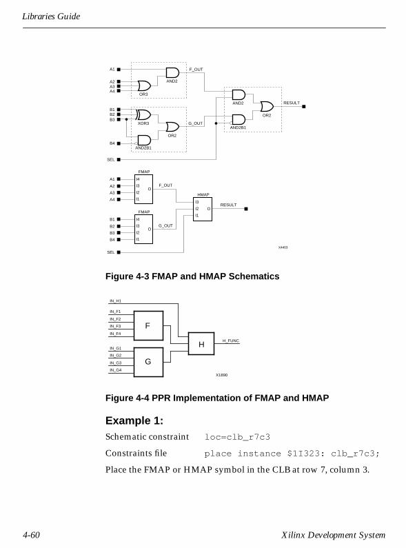
Libraries Guide
Figure 4-3 FMAP and HMAP Schematics
Figure 4-4 PPR Implementation of FMAP and HMAP
Example 1:Schematic constraint loc=clb_r7c3
Constraints file place instance $1I323: clb_r7c3;
Place the FMAP or HMAP symbol in the CLB at row 7, column 3.
X4403
A1
A2A3A4
B1B2B3
B4
SEL
A1 I4
FMAP
F_OUTI3
I2
I1
A2O
A3
A4
AND2
F_OUT
G_OUT
AND2
AND2B1
OR2
RESULT
OR3
XOR3
AND2B1
OR2
B1 I4
FMAP
G_OUTI3
I2
I1
B2O
I3
HMAP
RESULTI2
I1
O
B3
B4
SEL
IN_H1
IN_F1
IN_F2
IN_F3
IN_F4
F
HH_FUNC
G
IN_G1
IN_G2
IN_G3
IN_G4X1890
4-60 Xilinx Development System

Attributes, Constraints, and Carry Logic
Example 2:Schematic constraint loc=clb_r2c4;loc=clb_r3c4
Constraints file place instance top/dec0011:clb_r2c4 clb_r3c4;
Place the FMAP or HMAP symbol in either the CLB at row 2, column4 or the CLB at row 3, column 4.
Example 3:Schematic constraint loc=clb_r5c5:clb_r10c8
Constraints file place instance $3I27: [clb_r5c5clb_r10c8;
Place the FMAP or HMAP symbol in the area bounded by CLB R5C5in the upper left corner and CLB R10C8 in the lower right.
Example 4:Schematic constraint loc=clb_r10c11.f
Constraints file place instance top/done:clb_r1011.f;
Place the FMAP in the F function generator of CLB R10C11. The .Gextension specifies the G function generator. An HMAP can only gointo the H function generator, so there is no need to specify this place-ment explicitly.
CLBMAP ConstraintsWith the CLBMAP symbol, you can specify logic mapping at theschematic level for all XC3000 designs. It is used in conjunction withstandard logic elements, such as gates and flip-flops. It implicitlyspecifies the configuration of a CLB by defining the signals on itspins. Use the CLBMAP symbol to control mapping when the defaultmapping is not acceptable.
Enter the CLBMAP symbol on the schematic and assign signals to itspins. XNFMAP processes this symbol and maps the appropriatelogic, as defined by the input and output signals, into one CLB. Theeasiest way to define a CLBMAP is to connect a labeled wire segment
Libraries Guide 4-61

Libraries Guide
to each pin, which connects that pin to the net carrying the samelabel.
If a CLBMAP specifies an illegal CLB configuration, XNFMAPignores the CLBMAP and issues a warning explaining why theCLBMAP is illegal.
A CLBMAP can be either closed or open. A closed CLBMAP mustspecify both the input and output signals for that CLB. XNFMAPmaps a closed CLBMAP exactly as specified, unless the indicatedconfiguration is illegal. XNFMAP does not add any logic to a CLBspecified with a closed CLBMAP.
An open CLBMAP specifies only the output signals for the CLB.XNFMAP assigns those signals to the CLB output pins and maps thesource logic into the CLB as appropriate. Use an open CLBMAP tospecify the function of a CLB without specifying the exact configura-tion.
Specify whether a CLBMAP is either open or closed by attaching theappropriate MAP attribute to the symbol. See Table 4-10 for the exactconventions.
The pins on a CLBMAP can be either locked or unlocked. Specifywhether a CLBMAP has locked or unlocked pins by attaching theappropriate MAP attribute to the symbol. See Table 4-10 for the exactconventions. With an open CLBMAP, only the output pins are locked.
If a CLBMAP is indicated as having unlocked pins, you can lock indi-vidual CLBMAP pins by attaching a P (pin-lock) attribute to thecorresponding net. On an open CLBMAP, you can assign P attributesonly to output pins.
Table 4-10 Map Attributes for CLBMAP Symbols
Closed CLB Open CLB
Pins locked MAP=PLC MAP=PLO
Pins unlocked MAP=PUC MAP=PUO
4-62 Xilinx Development System

Attributes, Constraints, and Carry Logic
Example 1:Schematic constraint loc=CB
Constraints file place block top/cntq7: CB;
Place the CLBMAP in the CB CLB.
Example 2:Schematic constraint loc=AA:EE
Constraints file place block reg/bit7: [AA:EE];
Place the CLBMAP in the area bounded by CLB AA in the upper leftcorner and CLB EE in the lower right.
CLB ConstraintsYou can prohibit PPR from using a specific CLB, a range of CLBs, or arow or column of CLBs. Such prohibit constraints can be assignedonly through the constraints file. CLBs are prohibited by specifying aNotplace Instance constraint with only a wildcard (*) character as theinstance name, as shown in the following examples.
Example 1:Schematic constraint None
Constraints file notplace instance *: clb_r1c5;
Do not place any logic in the CLB in row 1, column 5. CLB R1C5 is inthe upper left corner of the device.
Example 2:Schematic constraint None
Constraints file notplace instance *: [clb_r1c1clb_r5c7];
Do not place any logic in the rectangular area bounded by the CLBR1C1 in the upper left corner and CLB R5C7 in the lower right.
Libraries Guide 4-63

Libraries Guide
Example 3:Schematic constraint None
Constraints file notplace instance *: clb_r*c3;
Do not place any logic in any row of column 3. The wildcard (*) char-acter can be used in place of either the row or column number tospecify an entire row or column of CLBs.
Example 4:Schematic constraint None
Constraints file notplace instance *: clb_r2c4clb_r7c9;
Do not place any logic in either CLB R2C4 or CLB R7C9.
I/O ConstraintsYou can constrain I/Os to one edge of the die, half an edge of the die,or a specific IOB. I/O constraints can be assigned from the schematicor through the CST file.
From the schematic, attach LOC constraints to the target PAD symbol.The constraints are then passed into the XNF and XTF files and readby PPR. For more information on attaching LOC constraints, see theappropriate interface user guide.
A pad can be found in the XNF file as an EXT record. Assume thefollowing lines appear in the XNF file.
ext, /top-102/data0, i,, blknm=data0ext, /top-117/q13, o,, blknm=out13
For a CST file constraint, the instance names of these I/Os are /top-102/data0_pad and /top-117/q13_pad.
Example 1:This example uses a pin number to lock to one pin.
Schematic constraint loc=p17
Constraints file place instance /top-102/data0_pad: p17;
4-64 Xilinx Development System

Attributes, Constraints, and Carry Logic
Place the I/O in the IOB at pin 17. For pin grid arrays, a pin namesuch as B3 or T1 is used.
Example 2:The following example uses a letter to lock to a side of the die.
Schematic constraint loc=t
Constraints file place instance /top-117/q13_pad: t;
Place the I/O in any IOB on the top edge of the die. Table 4-11 showsthe legal edge designations.
Table 4-11 Legal Edge Designations for IOBs
Note: When assigning global location constraints specifically to IOBsand edge decoders, refer to the die locations, not the package loca-tions. The package edges do not necessarily correspond to the dieedges. The die locations are rotated with respect to the package loca-tions. The only way to see where these edges are is to load the designinto EditLCA. See the EditLCA section in the “XACT Design Editor”chapter of the XACT Reference Guide for additional information.
Example 3:This example uses multiple locations.
Schematic constraint loc=t;loc=b
Constraints file place instance /top-117/q13_pad: t b;
Place the I/O in any IOB on the top or bottom edges of the die.
Edge Code Edge Location
b Bottom edge
l Left edge
r Right edge
t Top edge
Libraries Guide 4-65

Libraries Guide
Example 4:A two-letter combination is used to lock to a half-edge in thefollowing example.
Schematic constraint loc=tl
Constraints file place instance /top-102/data0_pad: tl;
Place the I/O in any IOB on the left half of the top edge of the die.Table 4-12 shows the legal half-edge designations.
Table 4-12 Legal Half-Edge Designations for IOBs
Example 5:This example constrains I/Os to the right edge of the IOB.
Schematic constraint loc=r
Constraints file place instance /top-117/q*_pad:r;
Place the I/Os in the IOBs on the right edge of the die.
From the schematic, the LOC constraint is attached to all target PADsymbols.
In the CST file, the wildcard (*) character specifies all instances thatbegin with /top-117/q and end with _pad. It identifies the externalsignals /top-117/q0_pad, /top-117/q1_pad, and so on.
Half-Edge Code Edge Location
TL Left half of top edge
TR Right half of top edge
BL Left half of bottom edge
BR Right half of bottom edge
LT Top half of left edge
LB Bottom half of left edge
RT Top half of right edge
RB Bottom half of right edge
4-66 Xilinx Development System
Attributes, Constraints, and Carry Logic
IOB ConstraintsYou can prohibit PPR from using a specific IOB. This step might betaken to keep user I/O signals away from semi-dedicated configura-tion pins. Such prohibit constraints can be assigned only through theCST file.
IOBs are prohibited by specifying a Notplace Instance constraint withonly a wildcard (*) character as the instance name, as shown in thefollowing example.
Schematic constraint None
Constraints file notplace instance *: p36 p37p41;
Do not place user I/Os in the IOBs at pins 36, 37, or 41. For pin gridarrays, pin names such as D14, C16, or H15 are used.
BUFT ConstraintsYou can constraint 3-state buffers to a specific BUFT, a range ofBUFTs, or a row or column of BUFTs. BUFT constraints can beassigned from the schematic or through the CST file. BUFTconstraints all refer to locations with a prefix of TBUF, which is thename of the physical element on the device.
From the schematic, LOC constraints are attached to the target BUFT.The constraints are then passed into the XNF and XTF files and readby PPR. For more information on attaching LOC constraints, see theappropriate user interface guide.
In a constraints file, a BUFT is identified by a unique instance name.A BUFT instance can found in the XNF file. Assume the followinglines appear in the XNF file. A BUFT symbol can be translated to theequivalent TBUF type.
sym, /top-72/rd0, TBUFsym, /top-79/ed7, TBUF
The instance names of these two BUFTs are /top-72/rd0 and/top-79/ed7. These names are used in the following examples.
Libraries Guide 4-67

Libraries Guide
Example 1:This example specifies BUFTs adjacent to a specific CLB.
Schematic constraint loc=TBUF_r1c5
Constraints file place instance /top-72/rd0:TBUF_r1c5;
Place the BUFT adjacent to CLB R1C5. You can use either the longlineabove the row of CLBs or the longline below.
Example 2:The following example places a specific BUFT.
Schematic constraint loc=TBUF_r1c5.1
Constraints file place instance /top-72/rd0:TBUF_r1c5.1;
Place the BUFT adjacent to CLB R1C5. The .1 tag specifies the longlineabove the row of CLBs. The .2 tag specifies the longline below it.
BUFTs that drive the same signal must carry consistent constraints. Ifyou specify the longline for one BUFT constraint, you must specify itfor all constraints on that line of BUFTs. However, not all BUFTs on aline need be constrained. Constraining one BUFT to a specificlongline forces the remaining BUFTs onto that line.
Example 3:The next example specifies a column of BUFTs.
Schematic constraint loc=TBUF_r*c3
Constraints file place instance /top-72/rd0top-79/ed7:TBUF_r*c3;
Place BUFTs in column 3 on any row. This constraint might be used toalign BUFTs with a common enable signal. You can use the wildcard(*) character in place of either the row or column number to specifyan entire row or column of BUFTs.
From the schematic, the same LOC constraint is attached to bothBUFTs.
4-68 Xilinx Development System

Attributes, Constraints, and Carry Logic
Example 4:This example specifies a row of BUFTs.
Schematic constraint loc=TBUF_r7c*
Constraints file place instance /top-79/ed7:TBUF_r7c*;
Place the BUFT on either the top or bottom horizontal longline in row7, in any column. You can use the wildcard (*) character in place ofeither the row or column number to specify an entire row or columnof BUFTs.
Edge Decoder ConstraintsEdge decoders can only be constrained to a single edge of the die;they cannot be split across two edges of the die. If you use decoderconstraints, you must assign all decode inputs for a given function tothe same edge. From the schematic, attach LOC constraints to thedecode logic — either a DECODE macro or a WAND gate with theDECODE attribute. The constraints are then passed into the XNF andXTF files and read by PPR. For more information on attaching LOCconstraints, see the appropriate interface user guide.
Here is an example:
Schematic constraint loc=T
Constraints file place instance dec1/$1I1:T;
Place the decoder along the top edge of the die. Table 4-13 shows thelegal edge designations.
Table 4-13 Legal Edge Designations for Edge Decoders
Edge Code Edge Location
T Top edge
B Bottom edge
L Left edge
R Right edge
TL Left half of top edge
Libraries Guide 4-69

Libraries Guide
To constrain decoders to precise positions within a side, constrain theassociated pads. However, because PPR determines decoder edgesbefore processing pad constraints, it is not enough to constrain thepads alone. To constrain decoders to a specific die side, use thefollowing rule. For every output net that you want to constrain,specify the side for at least one of its input decoders (WAND gates),using one of the following.
LOC=LLOC=TLOC=RLOC=B
Global Buffer ConstraintsYou can constrain a global buffer — BUFGP or BUFGS — to a cornerof the die. From the schematic, attach LOC constraints to the globalbuffer symbols. The constraints are then passed into the XNF andXTF files and read by PPR. For more information on attaching LOCconstraints, see the appropriate interface user guide.
Here is an example:
Schematic constraint loc=TL
Constraints file place instance buf1:TL;
Place the global buffer in the top left corner of the die. Table 4-14shows the legal corner designations.
TR Right half of top edge
BL Left half of bottom edge
BR Right half of bottom edge
LT Top half of left edge
LB Bottom half of left edge
RT Top half of right edge
RB Bottom half of right edge
Edge Code Edge Location
4-70 Xilinx Development System

Attributes, Constraints, and Carry Logic
Table 4-14 Legal Corner Designations for Global Buffers
If a global buffer is sourced by an external signal, the dedicated IOBfor that buffer must not be used by any other signal. For example, if aBUFGP is constrained to TL, the PGCK1 pin must be used to sourceit, and no other I/O can be assigned to that pin.
Relative Location (RLOC) ConstraintsThis section describes the relative location (RLOC) constraint, RLOCsets, and RLOC set constraints and modifiers.
DescriptionRelative location constraints group logic elements into discrete sets.You can define the location of any element within the set relative toother elements in the set, regardless of eventual placement in theoverall design. For example, if RLOC constraints are applied to agroup of eight flip-flops organized in a column, PPR maintains thecolumnar order and moves the entire group of flip-flops as a singleunit. In contrast, absolute location (LOC) constraints constrain designelements to specific locations on the FPGA die with no relation toother design elements.
RLOC constraints allow you to place logic blocks relative to eachother to increase speed, use die resources efficiently, and take advan-tage of the special carry logic built into the control logic blocks (CLBs)of the XC4000 devices. They provide an order and structure to relateddesign elements without requiring you to specify their absoluteplacement on the FPGA die. They allow you to replace any existinghard macro with an equivalent that can be directly simulated.
The relationally placed macro (RPM) library, which replaces the hardmacro library, uses RLOC constraints to define the order and
Corner Code Corner Location
TL Top left corner
TR Top right corner
BL Bottom left corner
BR Bottom right corner
Libraries Guide 4-71

Libraries Guide
structure of the underlying design primitives. The RPM library offersthe functionality and precision of the hard macro library with addedflexibility. You can optimize RPMs and merge other logic withinthem. Because these macros are built upon standard schematic parts,they do not have to be translated before simulation.
In the Unified Libraries, you can use RLOC constraints with BUFT-and CLB-related primitives, that is, DFF, HMAP, FMAP, and CY4primitives. You can also use them on non-primitive macro symbols.There are some restrictions on the use of RLOC constraints on BUFTsymbols. See the section on the RLOC_ORIGIN attribute later in thischapter. However, you cannot use RLOC constraints with decoders,clocks, or I/O primitives. LOC constraints, on the other hand, can beused on all primitives: BUFTs, CLBs, IOBs, decoders, and clocks.
The libraries created before the release of the Unified Libraries do notinclude RLOC constraints on the primitive symbols below the macrosymbols. To add RLOC constraints to the underlying macro primi-tives, make a copy of the library in your local directory and add theRLOC=R0C0 constraint to the underlying primitives. You can alsoattach RLOC constraints directly to non-macro primitives as you canfor the Unified Libraries.
The following symbols (primitives) accept RLOCs:
FDCEFDPEFMAPHMAPRAM16X1RAM32X1ROM16X1ROM32X1BUFT
SyntaxThe syntax of the RLOC constraint is the following:
RLOC = R row#Ccolumn#[. extension]
where the optional .extension can take all the values that are availablewith the current absolute LOC syntax: FFX, FFY, F, G, H, 1, and 2. The1 and 2 values are available for BUFT primitives, and the rest are
4-72 Xilinx Development System

Attributes, Constraints, and Carry Logic
available for primitives associated with CLBs. Only extensions for theXC4000 family designs are currently supported.
The row and column numbers can be any positive integer, includingzero. Absolute die locations, in contrast, cannot have zero as a row orcolumn number. Because row and column numbers in RLOCconstraints define only the order and relationship between designelements and not their absolute die locations, their numbering caninclude zero. Even though you can use any positive integer innumbering rows and columns for RLOC constraints, it is recom-mended that you use small integers for clarity and ease of use.
It is not the absolute values of the row and column numbers that isimportant in RLOC specifications but their relative values or differ-ences. For example, if design element A has an RLOC=R3C4constraint and design element B has an RLOC=R6C7 constraint, theabsolute values of the row numbers (3 and 6) are not important inthemselves. However, the difference between them is important; inthis case, 3 (6 -3) specifies that the location of design element B isthree rows away from the location of design element A. To capturethis information, a normalization process is used at some point in thedesign implementation. In the example just given, normalizationwould reduce the RLOC on design element A to R0C0, and the RLOCon design element B to R3C3.
In Xilinx programs, rows are numbered in increasing order from topto bottom, and columns are numbered in increasing order from left toright. RLOC constraints follow this numbering convention.
Figure 4-5a demonstrates the use of RLOC constraints. Four flip-flopprimitives named A, B, C, and D are assigned RLOC constraints asshown. These RLOC constraints require each flip-flop to be placed ina different CLB in the same column and stacked in the order shown:A above B, C, and D. Within a CLB, however, they can be placedeither in the FFX or FFY position.
If you wish to place more than one of these flip-flop primitives perCLB, you can specify the RLOCs as shown in Figure 4-5b. Thearrangement in Figure 4-5b requires that A and B be placed in asingle CLB and that C and D be placed in another CLB immediatelybelow the AB CLB. However, within a CLB, the flip-flops can beplaced in either of the two flip-flop positions, FFX or FFY.
Libraries Guide 4-73
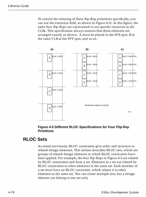
Libraries Guide
To control the ordering of these flip-flop primitives specifically, youcan use the extension field, as shown in Figure 4-5c. In this figure, thesame four flip-flops are constrained to use specific resources in theCLBs. This specification always ensures that these elements arearranged exactly as shown: A must be placed in the FFX spot, B inthe same CLB at the FFY spot, and so on.
Figure 4-5 Different RLOC Specifications for Four Flip-flopPrimitives
RLOC SetsAs noted previously, RLOC constraints give order and structure torelated design elements. This section describes RLOC sets, which aregroups of related design elements to which RLOC constraints havebeen applied. For example, the four flip-flops in Figure 4-5 are relatedby RLOC constraints and form a set. Elements in a set are related byRLOC constraints to other elements in the same set. Each member ofa set must have an RLOC constraint, which relates it to otherelements in the same set. You can create multiple sets, but a designelement can belong to one set only.
X4292
RLOC = R0C0A
(a)
RLOC = R1C0B
RLOC = R2C0C
RLOC = R3C0D
(b)
RLOC = R0C0.FFXA
(c)
RLOC = R1C0.FFXC
RLOC = R0C0.FFYB
RLOC = R1C0.FFYD
RLOC = R0C0A
RLOC = R1C0C
RLOC = R0C0B
RLOC = R1C0D
Shaded lines indicate a CLB grid.
4-74 Xilinx Development System

Attributes, Constraints, and Carry Logic
Sets can be defined in several ways: explicitly through the use of aset parameter or implicitly through the structure of the design hier-archy.
There are four distinct types of rules associated with each set:
● Definition rules define the requirements for membership in a set.
● Linkage rules specify how elements can be linked to other ele-ments to form a single set.
● Modification rules dictate how to specify parameters that modifyRLOC values of all the members of the set.
● Naming rules specify the nomenclature of sets.
These rules are discussed in the sections that follow.
The following sections discuss three different set constraints: U_SET,H_SET, and HU_SET. Elements must be tagged with both the RLOCconstraint and one of these set constraints to belong to a set.
U_SETU_SET constraints enable you to group into a single set designelements with attached RLOC constraints that are distributedthroughout the design hierarchy. The letter U in the name U_SETindicates that the set is user-defined. U_SET constraints allow you togroup elements, even though they are not directly related by thedesign hierarchy. By attaching a U_SET constraint to design elements,you can explicitly define the members of a set. The design elementstagged with a U_SET constraint can exist anywhere in the designhierarchy; they can be primitive or non-primitive symbols. Whenattached to non-primitive symbols, the U_SET constraint propagatesto all the primitive symbols with RLOC constraints that are below itin the hierarchy.
The syntax of the U_SET constraint is the following:
U_SET=name
where name is the user-specified identifier of the set. All designelements with RLOC constraints tagged with the same U_SETconstraint name belong to the same set. Names therefore must beunique among all the sets in the design.
Libraries Guide 4-75

Libraries Guide
H_SETIn contrast to the U_SET constraint, which you explicitly define bytagging design elements, the H_SET (hierarchy set) is defined implic-itly through the design hierarchy. The combination of the design hier-archy and the presence of RLOC constraints on elements defines ahierarchical set, or H_SET set. You do not use an HSET constraint totag the design elements to indicate their set membership. The set isdefined automatically by the design hierarchy. All design elementswith RLOC constraints at a single node of the design hierarchy areconsidered to be in the same H_SET set unless they are tagged withanother type of set constraint such as RLOC_ORIGIN orRLOC_RANGE. These constraints are discussed later in this chapter.If you explicitly tag any element with an RLOC_ORIGIN,RLOC_RANGE, U_SET, or HU_SET constraint, it is removed from anH_SET set. Most designs contain only H_SET constraints, since theyare the underlying mechanism for relationally placed macros.
The design-flattening program, XNFMerge, recognizes the implicitH_SET set, derives its name, or identifier, attaches the H_SETconstraint to the correct members of the set, and writes them to theoutput file.
The syntax of the H_SET constraint as generated by XNFMergefollows:
H_SET=name
Name is the identifier of the set and is unique among all the sets in thedesign. The base name for any H_SET is “hset,” to which XNFMergeadds a hierarchy path prefix to obtain unique names for differentH_SET sets in the XNFMerge output file.
4-76 Xilinx Development System
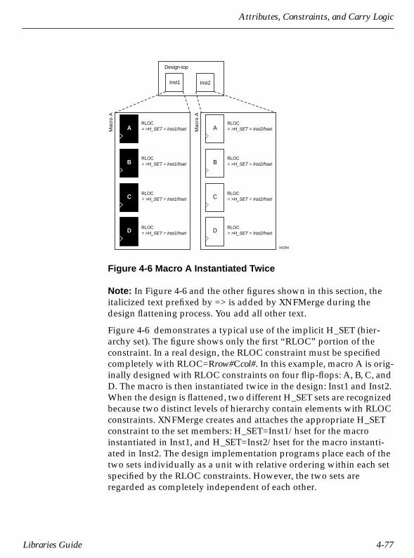
Attributes, Constraints, and Carry Logic
Figure 4-6 Macro A Instantiated Twice
Note: In Figure 4-6 and the other figures shown in this section, theitalicized text prefixed by => is added by XNFMerge during thedesign flattening process. You add all other text.
Figure 4-6 demonstrates a typical use of the implicit H_SET (hier-archy set). The figure shows only the first “RLOC” portion of theconstraint. In a real design, the RLOC constraint must be specifiedcompletely with RLOC=Rrow#Ccol#. In this example, macro A is orig-inally designed with RLOC constraints on four flip-flops: A, B, C, andD. The macro is then instantiated twice in the design: Inst1 and Inst2.When the design is flattened, two different H_SET sets are recognizedbecause two distinct levels of hierarchy contain elements with RLOCconstraints. XNFMerge creates and attaches the appropriate H_SETconstraint to the set members: H_SET=Inst1/hset for the macroinstantiated in Inst1, and H_SET=Inst2/hset for the macro instanti-ated in Inst2. The design implementation programs place each of thetwo sets individually as a unit with relative ordering within each setspecified by the RLOC constraints. However, the two sets areregarded as completely independent of each other.
Design-top
RLOC= >H_SET = Inst2/hsetA
X4294
B
C
D
Inst1 Inst2
Macr
o A
RLOC= >H_SET = Inst2/hset
RLOC= >H_SET = Inst2/hset
RLOC= >H_SET = Inst2/hset
RLOC= >H_SET = Inst1/hsetA
B
C
D
Macr
o A
RLOC= >H_SET = Inst1/hset
RLOC= >H_SET = Inst1/hset
RLOC= >H_SET = Inst1/hset
Libraries Guide 4-77

Libraries Guide
The name of the H_SET set is derived from the symbol or node in thehierarchy that includes all the RLOC elements. In Figure 4-6, Inst1 isthe node (instantiating macro) that includes the four flip-flopelements with RLOCs shown on the left of Figure 4-6. Therefore, thename of this H_SET set is the hierarchically qualified name of “Inst1”followed by “hset.” The Inst1 symbol is considered the “start” of theH_SET, which gives a convenient handle to the entire H_SET andattaches constraints that modify the entire H_SET. Constraints thatmodify sets are discussed later in this chapter.
Figure 4-6 demonstrates the simplest use of a set that is defined andconfined to a single level of hierarchy. Through linkage and modifica-tion, you can also create an H_SET set that is linked through two ormore levels of hierarchy. Linkage allows you to link elements throughthe hierarchy into a single set. On the other hand, modification allowsyou to modify RLOC values of the members of a set through the hier-archy.
Set LinkageThe example in Figure 4-7 explains and illustrates the process oflinking together elements through the design hierarchy. Again, thecomplete RLOC specification, RLOC=Rrow#Ccol#, is required for areal design.
Note: In this and other illustrations in this section, the sets are shadeddifferently to distinguish one set from another.
4-78 Xilinx Development System

Attributes, Constraints, and Carry Logic
Figure 4-7 Three H_SET Sets
As noted previously, all design elements with RLOC constraints at asingle node of the design hierarchy are considered to be in the sameH_SET set unless they are assigned another type of set constraint, anRLOC_ORIGIN constraint, or an RLOC_RANGE constraint. InFigure 4-7, RLOC constraints have been added on primitives andnon-primitives C, D, F, G, H, I, J, K, M, N, O, P, Q, and R. No RLOCconstraints were placed on B, E, L, or S. Macros C and D have anRLOC constraint at node A, so all the primitives below C and D thathave RLOCs are members of a single H_SET set. Furthermore, thename of this H_SET set is “A/hset” because it is at node A that the setstarts. The start of an H_SET set is the lowest common ancestor of allthe RLOC-tagged constraints that constitute the elements of that
RLOC
= > H_SET = A/hset
X4295
Design-top
A
G
F
B
C D ERLOC RLOC
H
I
RLOC
= > H_SET = A/hset
RLOC
= > H_SET = A/hset
RLOC
= > H_SET = A/hset
RLOC
= > H_SET = A/hset
K
J
RLOC
= > H_SET = A/hset
L
RLOC
= > H_SET = A/hset
P
O
RLOC
= > H_SET = A/hset
RLOC
= > H_SET = A/D/L/hsetQ
RLOC
= > H_SET = A/D/L/hsetR
S
RLOC
= > H_SET = A/E/hset
N
M
RLOC
= > H_SET = A/E/hset
Libraries Guide 4-79

Libraries Guide
H_SET set. Because element E does not have an RLOC constraint, it isnot linked to the A/hset set. The RLOC-tagged elements M and N,which lie below element E, are therefore in their own H_SET set. Thestart of that H_SET set is A/E, giving it the name “A/E/hset.”
Similarly, the Q and R primitives are in their own H_SET set becausethey are not linked through element L to any other design elements.The lowest common ancestor for their H_SET set is L, which gives itthe name “A/D/L/hset.” After the flattening, XNFMerge attachesH_SET=A/hset to the F, G, H, O, P, J, and K primitives; H_SET=A/D/L/hset to the Q and R primitives; and H_SET=A/E/hset to the Mand N primitives.
Consider a situation in which a set is created at the top of the design.In Figure 4-7, there would be no lowest common ancestor if macro Aalso had an RLOC constraint, since A is at the top of the design andhas no ancestor. In this case, the base name “hset” would have nohierarchically qualified prefix, and the name of the H_SET set wouldsimply be “hset.”
Set ModificationAs noted earlier, the RLOC constraint assigns a primitive an RLOCvalue (the row and column numbers with the optional extensions),specifies its membership in a set, and links together elements atdifferent levels of the hierarchy. In Figure 4-7, the RLOC constraint onmacros C and D links together all the objects with RLOC constraintsbelow them. An RLOC constraint is also used to modify the RLOCvalues of constraints below it in the hierarchy. In other words, RLOCvalues of elements affect the RLOC values of all other memberelements of the same H_SET set that lie below the given element inthe design hierarchy.
When the design is flattened, the row and column numbers of anRLOC constraint on an element are added to the row and columnnumbers of the RLOC constraints of the set members below it in thehierarchy. This feature gives you the ability to modify existing RLOCvalues in submodules and macros without changing the previouslyassigned RLOC values on the primitive symbols. This modificationprocess also applies to the optional extension field. However, whenusing extensions for modifications, you must ensure that inconsistentextensions are not attached to the RLOC value of a design elementthat may conflict with RLOC extensions placed on underlying
4-80 Xilinx Development System

Attributes, Constraints, and Carry Logic
elements. For example, if an element has an RLOC constraint withthe FFX extension, all the underlying elements with RLOCconstraints must either have the same extension, in this case FFX, orno extension at all; any underlying element with an RLOC constraintand an extension different from FFX, such as FFY or F, is flagged as anerror. After resolving all the RLOC constraints, extensions that arenot valid on primitives are removed from those primitives. Forexample, if XNFMerge generates an FFX extension to be applied on aprimitive after propagating the RLOC constraints, it applies theextension if and only if the primitive is a flip-flop. If the primitive isan element other than a flip-flop, the extension is ignored. Only theextension is ignored in this case, not the entire RLOC constraint.
Figure 4-8 illustrates the process of adding RLOC values down thehierarchy. The row and column values between the parentheses showthe addition function performed by XNFMerge. The italicized textprefixed by => is added by XNFMerge during the design flatteningprocess and replaces the original RLOC constraint that you added.
Figure 4-8 Adding RLOC Values Down the Hierarchy
A
Design-top
RLOC = R2C3
RLOC = R0C0 (+R2C3)
= >RLOC = R2C3
E
B
RLOC = R0C0 (+R5C3.FFX)= >RLOC = R5C3.FFXF
G
X4296
C
D
RLOC = R1C0 (+R2C3)
= >RLOC = R3C3
RLOC = R2C0 (+R2C3)
= >RLOC = R4C3
RLOC = R3C0.FFX (+R2C3)
= >RLOC = R5C3.FFX
XNFMerge addsR5C3.FFX below tocreate new RLOC
RLOC = R1C0 (+R5C3.FFX)= >RLOC = R6C3.FFX
XNFMerge addsR2C3 below tocreate new RLOC
Libraries Guide 4-81

Libraries Guide
The ability to modify RLOC values down the hierarchy is particularlyvaluable when instantiating the same macro more than once. Typi-cally, macros are designed with RLOC constraints that are modifiedwhen the macro is instantiated. Figure 4-9 is a variation of thesample design in Figure 4-6. The RLOC constraint on Inst1 and Inst2now link all the objects in one H_SET set. Because the RLOC=R0C0modifier on the Inst1 macro does not affect the objects below it,XNFMerge only adds the H_SET tag to the objects and leaves theRLOC values as they are. However, the RLOC=R0R1 modifier on theInst2 macro causes XNFMerge to change the RLOC values on objectsbelow it, as well as to add the H_SET tag, as shown in the italicizedtext.
Figure 4-9 Modifying RLOC Values of Same Macro and LinkingTogether as One Set
HU_SETThe HU_SET constraint is a variation of the implicit H_SET (hier-archy set). Like H_SET, HU_SET is defined by the design hierarchy.However, you can use the HU_SET constraint to assign a user-defined name to the HU_SET.
The syntax of the HU_SET constraint is the following:
HU_SET=name
Design-top
RLOC = R0C1
RLOC = R0C0 (+R0C1)
= >H_SET = hsetA
X4297
B
C
add R0C1 to shiftthe set 1 columnto the right
D
RLOC = R0C0
Inst1 Inst2
= >RLOC = R0C1
RLOC = R1C0 (+R0C1)
= >H_SET = hset= >RLOC = R1C1
RLOC = R2C0 (+R0C1)
= >H_SET = hset= >RLOC = R2C1
RLOC = R3C0 (+R0C1)
= >H_SET = hset= >RLOC = R3C1
Mac
ro A
RLOC = R0C0
= >H_SET = hsetA
B
C
D
Mac
ro A
RLOC = R1C0
= >H_SET = hset
RLOC = R2C0
= >H_SET = hset
RLOC = R3C0
= >H_SET = hset
add R0C0—nochange
4-82 Xilinx Development System

Attributes, Constraints, and Carry Logic
where name is the identifier of the set; it must be unique among all thesets in the design. You must define the base names to ensure uniquehierarchically qualified names for the sets after XNFMerge flattensthe design and attaches the hierarchical names as prefixes.
This user-defined name is the base name of the HU_SET set. Like theH_SET set, in which the base name of “hset” is prefixed by the hierar-chical name of the lowest common ancestor of the set elements, theuser-defined base name of an HU_SET set is prefixed by the hierar-chical name of the lowest common ancestor of the set elements.
The HU_SET constraint defines the start of a new set: all designelements at the same node that have the same user-defined value forthe HU_SET constraint are members of the same HU_SET set. Alongwith the HU_SET constraint, elements can also have an RLOCconstraint. The presence of an RLOC constraint in an H_SETconstraint links the element to all elements tagged with RLOCs aboveand below in the hierarchy. However, in the case of an HU_SETconstraint, the presence of an RLOC constraint along with theHU_SET constraint on a design element does not automatically linkthe element to other elements with RLOC constraints at the samehierarchy level or above.
Libraries Guide 4-83

Libraries Guide
Figure 4-10 HU_SET Constraint Linking and SeparatingElements from H_SET Sets
Figure 4-10 demonstrates how HU_SET constraints designateelements as set members, break links between elements tagged withRLOC constraints in the hierarchy to separate them from H_SET sets,and generate names as identifiers of these sets. The user-definedHU_SET constraint on E separates its underlying design elements,namely H, I, J, K, L, and M from the implicit H_SET=A/hset thatcontains primitive members B, C, F, and G. The HU_SET set that isdefined at E includes H, I, and L (through the element J). XNFMergehierarchically qualifies the name value “bar” on element E to be A/bar, since A is the lowest common ancestor for all the elements of theHU_SET set, and attaches it to the set member primitives H, I, and L.An HU_SET constraint on K starts another set that includes M, which
RLOC
= > H_SET = A/hset
X4298
Design-top
A
C
B
D
RLOC
= > H_SET = A/hset
RLOC E HU_SET = bar
RLOC
= > H_SET = A/hset
G
F
RLOC
= > H_SET = A/hset
RLOC
= > HU_SET = A/bar
I
H
J
RLOC
= > HU_SET = A/bar
RLOC K HU_SET = bar
RLOC
= > HU_SET = A/barL RLOC
= > HU_SET = A/E/barM
4-84 Xilinx Development System

Attributes, Constraints, and Carry Logic
receives the HU_SET=A/E/bar constraint after processing byXNFMerge. In Figure 4-10, the same name field is used for the twoHU_SET constraints, but because they are attached to symbols atdifferent levels of the hierarchy, they define two different sets.
Figure 4-11 Linking Two HU_SET Sets
Figure 4-11 shows how HU_SET constraints link elements in thesame node together by naming them with the same identifier.Because of the same name, “bar,” on two elements, D and E, theelements tagged with RLOC constraints below D and E become partof the same HU_SET.
Set ModifiersA modifier, as its name suggests, modifies the RLOC constraints asso-ciated with design elements. Since it modifies the RLOC constraintsof all the members of a set, it must be applied in a way that propa-gates it to all the members of the set easily and intuitively.
A
Design-top
RLOC
= > H_SET = A/hset
RLOC
HU_SET = barD E
C
B
RLOC
= > HU_SET = A/bar
RLOC
= > HU_SET = A/bar
G
F RLOC
= > HU_SET = A/bar
RLOC
= > HU_SET = A/bar
H
I
X4299
= > H_SET = A/hset
HU_SET = bar
Libraries Guide 4-85

Libraries Guide
For this reason, the RLOC modifiers of a set are placed at the start ofthat set. This section discusses the different modifiers that you canuse to modify the RLOC set constraints.
RLOCAs discussed previously, the RLOC constraint associated with adesign element modifies the values of other RLOC constraints belowthe element in the hierarchy of the set. Regardless of the set type,RLOC row, column, and extension values on an element always prop-agate down the hierarchy and are added at lower levels of the hier-archy to RLOC constraints on elements in the same set.
RLOC_ORIGINSpecifying RLOC constraints to describe the spatial relationship ofthe set members to themselves allows the members of the set to floatanywhere on the die as a unit. You can, however, fix the exact dielocation of the set members. The RLOC_ORIGIN constraint allowsyou to change the RLOC values into absolute LOC constraints thatrespect the structure of the set.
Following is the syntax of this constraint:
RLOC_ORIGIN=Rrow#Ccolumn#
where the row and column numbers are positive non-zero integervalues. When an RLOC_ORIGIN constraint is applied to a set, therow and column values of the RLOC_ORIGIN are added to the indi-vidual RLOC values of the members of the set to obtain a final LOCconstraint for each element in the set. Since the row and columnnumbers of an RLOC_ORIGIN constraint refer to actual die locations,its value must exclude zero.
Note: In the XACT 5.0 release, you must use the RLOC_ORIGIN con-straint with sets that include BUFT symbols. Sets with BUFT symbolsmust be fixed to an exact die location.
The design flattening program, XNFMerge, translates theRLOC_ORIGIN constraint into LOC constraints. The row and columnvalues of the RLOC_ORIGIN are added individually to the membersof the set after all RLOC modifications have been made to their rowand column values by addition through the hierarchy. The finalvalues are then turned into LOC constraints on individual primitives.
4-86 Xilinx Development System

Attributes, Constraints, and Carry Logic
When this constraint is used in conjunction with an implicit H_SET(hierarchy set), it must be placed on the element that is the start of theH_SET set, that is, on the lowest common ancestor of all the membersof the set. If you apply an RLOC_ORIGIN constraint to an HU_SETconstraint, place it on the element at the start of the HU_SET set, thatis, on an element with the HU_SET constraint. However, since therecould be several elements linked together with the HU_SETconstraint at the same node, the RLOC_ORIGIN constraint can beapplied to only one of these elements to prevent more than oneRLOC_ORIGIN constraint from being applied to the HU_SET set.Similarly, when used with a U_SET constraint, the RLOC_ORIGINconstraint can be placed on only one element with the U_SETconstraint. If you attach the RLOC_ORIGIN constraint to an elementthat has only an RLOC constraint, the membership of that element inany set is removed, and the element is considered the start of a newH_SET set with the specified RLOC_ORIGIN constraint attached tothe newly created set.
Libraries Guide 4-87

Libraries Guide
Figure 4-12 Using an RLOC_ORIGIN Constraint to Modify anH_SET Set
In Figure 4-12, the elements B, C, D, F, and G are members of anH_SET set with the name A/hset. This figure is the same as Figure 4-8 except for the presence of an RLOC_ORIGIN constraint at the startof the H_SET set (at A). The RLOC_ORIGIN values are added to theresultant RLOC values at each of the member elements to obtain thevalues that are then converted by XNFMerge to LOC constraints. Forexample, the RLOC value of F, given by adding the RLOC value at E(R0C1) and that at F (R0C0), is added to the RLOC_ORIGIN value(R2C3) to obtain the value of (R2C4), which is then converted to aLOC constraint, LOC = CLB_R2C4.
A
Design-top
RLOC_ORIGIN = R2C3
RLOC = R0C0 (+R2C3)
= >LOC = CLB_R2C3
RLOC = R0C1E
B
RLOC = R0C0 (+R0C1 + R2C3)
= >LOC = CLB_R2C4F
G
X4300
XNFMerge adds ROC1 and RLOC_ORIGIN(R2C3) below to get final LOC constraint
RLOC = R1C0 (+R0C1 + R2C3)
= >LOC = CLB_R3C4
RLOC = R1C0 (+R2C3)
= >LOC = CLB_R3C3C
RLOC = R2C0 (+R2C3)
= >LOC = CLB_R4C3D
XNFMerge adds RLOC_ORIGIN(R2C3) below to get final LOC constraint
4-88 Xilinx Development System
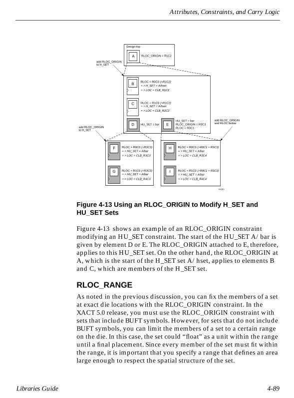
Attributes, Constraints, and Carry Logic
Figure 4-13 Using an RLOC_ORIGIN to Modify H_SET andHU_SET Sets
Figure 4-13 shows an example of an RLOC_ORIGIN constraintmodifying an HU_SET constraint. The start of the HU_SET A/bar isgiven by element D or E. The RLOC_ORIGIN attached to E, therefore,applies to this HU_SET set. On the other hand, the RLOC_ORIGIN atA, which is the start of the H_SET set A/hset, applies to elements Band C, which are members of the H_SET set.
RLOC_RANGEAs noted in the previous discussion, you can fix the members of a setat exact die locations with the RLOC_ORIGIN constraint. In theXACT 5.0 release, you must use the RLOC_ORIGIN constraint withsets that include BUFT symbols. However, for sets that do not includeBUFT symbols, you can limit the members of a set to a certain rangeon the die. In this case, the set could “float” as a unit within the rangeuntil a final placement. Since every member of the set must fit withinthe range, it is important that you specify a range that defines an arealarge enough to respect the spatial structure of the set.
A
Design-top
RLOC_ORIGIN = R1C2
RLOC = R0C0 (+R1C2)= > H_SET = A/hset
RLOC = R1C0 (+R1C2)
= > LOC = CLB_R2C2
HU_SET = bar RLOC_ORIGIN = R3C3HU_SET = bar
RLOC = R0C1D E
C
B
RLOC = R0C0 (+R3C3)= > HU_SET = A/bar
RLOC = R1C0 (+R3C3)= > HU_SET = A/bar
G
F RLOC = R0C0 (+R0C1 + R3C3)= > HU_SET = A/bar
RLOC = R1C0 (+R0C1 + R3C3)= > HU_SET = A/bar
H
I
X4301
add RLOC_ORIGINand RLOC below
add RLOC_ORIGINto H_SET
= > LOC = CLB_R1C2
= > H_SET = A/hset
= > LOC = CLB_R3C3
= > LOC = CLB_R4C3 = > LOC = CLB_R4C4
= > LOC = CLB_R3C4
add RLOC_ORIGINto H_SET
Libraries Guide 4-89
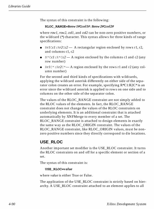
Libraries Guide
The syntax of this constraint is the following:
RLOC_RANGE=Rrow1#Ccol1#:R row2#Ccol2#
where row1, row2, col1, and col2 can be non-zero positive numbers, orthe wildcard (*) character. This syntax allows for three kinds of rangespecifications:
● Rr1Cc1:R r2Cc2 — A rectangular region enclosed by rows r1, r2,and columns c1, c2
● R*Cc1:R*C c2 — A region enclosed by the columns c1 and c2 (anyrow number)
● Rr1C*:R r2C*— A region enclosed by the rows r1 and r2 (any col-umn number)
For the second and third kinds of specifications with wildcards,applying the wildcard asterisk differently on either side of the sepa-rator colon creates an error. For example, specifying R*C1:R2C* is anerror since the wildcard asterisk is applied to rows on one side and tocolumns on the other side of the separator colon.
The values of the RLOC_RANGE constraint are not simply added tothe RLOC values of the elements. In fact, the RLOC_RANGEconstraint does not change the values of the RLOC constraints onunderlying elements. It is an additional constraint that is attachedautomatically by XNFMerge to every member of a set. TheRLOC_RANGE constraint is attached to design elements in exactlythe same way as the RLOC_ORIGIN constraint. The values of theRLOC_RANGE constraint, like RLOC_ORIGIN values, must be non-zero positive numbers since they directly correspond to die locations.
USE_RLOCAnother important set modifier is the USE_RLOC constraint. It turnsthe RLOC constraints on and off for a specific element or section of aset.
The syntax of this constraint is:
USE_RLOC=value
where value is either True or False.
The application of the USE_RLOC constraint is strictly based on hier-archy. A USE_RLOC constraint attached to an element applies to all
4-90 Xilinx Development System

Attributes, Constraints, and Carry Logic
its underlying elements that are members of the same set. If it isattached to a symbol that defines the start of a set, the constraint isapplied to all the underlying member elements, which represent theentire set. However, if it is applied to an element below the start ofthe set (for example, E in Figure 4-14), only the members of the set (Hand I) below the specified element are affected.You can also attach theUSE_RLOC constraint directly to a primitive symbol so that it affectsonly that symbol.
Figure 4-14 Using the USE_RLOC Constraint to Control RLOCApplication on H_SET and HU_SET Sets
When the USE_RLOC=false constraint is applied, the RLOC and setconstraints are removed from the affected symbols in the XNFMergeoutput file. This process is different than that followed for theRLOC_ORIGIN constraint. For RLOC_ORIGIN, XNFMerge gener-ates and outputs a LOC constraint in addition to all the set and RLOCconstraints in the output file. XNFMerge does not retain the original
A
Design-top
USE_RLOC = FALSE
RLOC = R0C0
= > H SET = A/hset
RLOC = R1C0
= > H SET = A/hset
HU_SET = bar
Parameters removed
Parameters removed
RLOC = R0C1HU_SET = bar
USE_RLOC = FALSED E
C
B
RLOC = R0C0
= > HU_SET = A/bar
RLOC = R1C0
= HU_SET = A/bar
G
F RLOC = R0C0
= > HU_SET = A/bar
RLOC = R1C0
= > HU_SET = A/bar
Parametersremoved
Parametersremoved
H
I
X4302
propagate USE_RLOCand removeset parametersbelow
applyUSE_RLOCto H_SET
Libraries Guide 4-91

Libraries Guide
constraints in the presence of a USE_RLOC=false constraint becausethese cannot be turned on again in later programs.
Figure 4-14 illustrates the use of the USE_RLOC constraint to mask anentire set as well as portions of a set.
Applying the USE_RLOC constraint on U_SET sets is a special casebecause of the lack of hierarchy in the U_SET set. Because theUSE_RLOC constraint propagates strictly in a hierarchical manner,the members of a U_SET set that are in different parts of the designhierarchy must be tagged separately with USE_RLOC constraints; nosingle USE_RLOC constraint is propagated to all the members of theset that lie in different parts of the hierarchy. If you create a U_SET setthrough an instantiating macro, you can attach the USE_RLOCconstraint to the instantiating macro to allow it to propagate hierar-chically to all the members of the set. You can create this instantiatingmacro by placing a U_SET constraint on a macro and lettingXNFMerge propagate that constraint to every symbol with an RLOCconstraint below it in the hierarchy.
Figure 4-15 illustrates an example of the use of the USE_RLOC=falseconstraint. The USE_RLOC=false on primitive E removes it from theU_SET set, and USE_RLOC=false on element F propagates to primi-tive G and removes it from the U_SET set.
Figure 4-15 Using the USE_LOC Constraint to Control RLOCApplication on U_Sets
Design-top
X4303
G
A
U_SET = barRLOC = R0C0C
D
EU_SET = bar
RLOC = R2C0
B
U_SET = barRLOC = R1C0
USE_RLOC = FALSE
FU_SET = bar
USE_RLOC = FALSE
U_SET = bar
RLOC = R3C0
propagate USE_RLOCand remove set parametersbelow
Parametersremoved
Parametersremoved
4-92 Xilinx Development System

Attributes, Constraints, and Carry Logic
While propagating the USE_RLOC constraint, XNFMerge ignoresunderlying USE_RLOC constraints if it encounters elements higherin the hierarchy that already have USE_RLOC constraints. Forexample, if XNFMerge encounters an underlying element with aUSE_RLOC=true constraint during the propagation of aUSE_RLOC=false constraint, it ignores the newly encountered Trueconstraint.
Xilinx MacrosXilinx-supplied flip-flop macros include an RLOC_R0C0 constrainton the underlying primitive, which allows you to attach an RLOC tothe macro symbol. This symbol links the underlying primitive to theset that contains the macro symbol. Simply attach an appropriateRLOC constraint to the instantiation of the actual Xilinx flip-flopmacro. XNFMerge adds the RLOC value that you specified to theunderlying primitive so that it has the desired value.
Figure 4-16 Typical Use of a Xilinx Macro
FD
RLOC=R0C0
QCE
DRC
FD
RLOC = R0C0 (+R1C1)
= > RLOC = R1C1
RLOC = R1C1
Inst 1
Propagate R1C1
FDRE Macro
FD
RE
X4304
Libraries Guide 4-93

Libraries Guide
For example, in Figure 4-16, the RLOC = R1C1 constraint is attachedto the instantiation (Inst1) of the FDRE macro. It is added to the R0C0value of the RLOC constraint on the flip-flop within the macro toobtain the new RLOC values.
If you do not put an RLOC constraint on the flip-flop macro symbol,the underlying primitive symbol is the lone member of a set.XNFMerge removes RLOC constraints from a primitive that is theonly member of a set or from a macro that has no RLOC objects belowit.
LOC Propagation Through Design FlatteningXNFMerge continues to propagate LOC constraints down the designhierarchy. It adds this constraint to appropriate objects that are notmembers of a set. While RLOC constraint propagation is limited tosets, the LOC constraint is applied from its start point all the waydown the hierarchy.
SummaryTable 4-15 summarizes the RLOC set types and the constraints thatidentify members of these sets.
Table 4-15 Summary of Set Types
Type Definition Naming Linkage Modification
Set A set is a collec-tion of elementsto which rela-tive locationconstraints areapplied.
U_SET=name
All elementswith the sameuser-taggedU_SET con-straint value aremembers of thesame U_SET set.
The name of theset is the same asthe user-definedname withoutany hierarchicalqualification.
U_SET links ele-ments to all otherelements with thesame value for theU_SET constraint.
U_SET is modi-fied by applyingRLOC_ORIGINor RLOC_RANGEconstraints on, atmost, one of theU_SET constraint-tagged elements.
4-94 Xilinx Development System
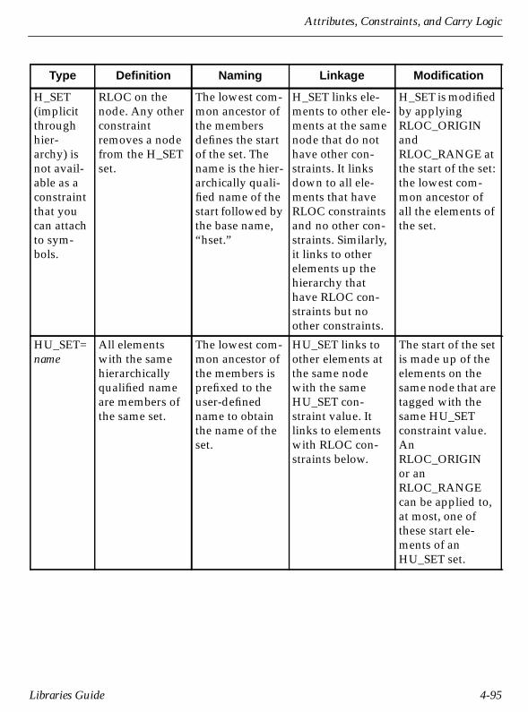
Attributes, Constraints, and Carry Logic
H_SET(implicitthroughhier-archy) isnot avail-able as aconstraintthat youcan attachto sym-bols.
RLOC on thenode. Any otherconstraintremoves a nodefrom the H_SETset.
The lowest com-mon ancestor ofthe membersdefines the startof the set. Thename is the hier-archically quali-fied name of thestart followed bythe base name,“hset.”
H_SET links ele-ments to other ele-ments at the samenode that do nothave other con-straints. It linksdown to all ele-ments that haveRLOC constraintsand no other con-straints. Similarly,it links to otherelements up thehierarchy thathave RLOC con-straints but noother constraints.
H_SET is modifiedby applyingRLOC_ORIGINandRLOC_RANGE atthe start of the set:the lowest com-mon ancestor ofall the elements ofthe set.
HU_SET=name
All elementswith the samehierarchicallyqualified nameare members ofthe same set.
The lowest com-mon ancestor ofthe members isprefixed to theuser-definedname to obtainthe name of theset.
HU_SET links toother elements atthe same nodewith the sameHU_SET con-straint value. Itlinks to elementswith RLOC con-straints below.
The start of the setis made up of theelements on thesame node that aretagged with thesame HU_SETconstraint value.AnRLOC_ORIGINor anRLOC_RANGEcan be applied to,at most, one ofthese start ele-ments of anHU_SET set.
Type Definition Naming Linkage Modification
Libraries Guide 4-95
Libraries Guide
Relationally Placed Macros (RPMs)The Xilinx libraries contain three types of elements.
● Primitives are basic logical elements such as AND2 and OR2gates.
● Soft macros are schematics made by combining primitives andsometimes other soft macros.
● Relationally placed macros (RPMs) are soft macros that containrelative location constraint (RLOC) information, carry logic sym-bols, and FMAP/HMAP symbols, where appropriate. RPMs arecurrently only available in the XC4000 library.
Designs created with RPMs can be functionally simulated.
The HM2RPM utility translates old custom hard macro files into RPMfiles. If you created your own hard macro files, you must runHM2RPM on each hard macro file and place the new XNF file in yourcurrent working directory or in a search directory specified forXNFMerge. For instructions on using the HM2RPM utility, see the“HM2RPM” chapter of the XACT Reference Guide.
RPMs can, but need not, include all the following elements:
● FMAPs, HMAPs, and CLB-grouping attributes to control map-ping. FMAPs and HMAPs have pin-lock attributes, which allowbetter control over routing. FMAPs and HMAPs are described inthe “Mapping Constraints” section of the “PPR Placement Con-straints” section earlier in this chapter.
● Relative location (RLOC) constraints to provide placement struc-ture. They allow positioning of elements relative to each other.They are discussed in the “Relative Location Constraints” sectionearlier in this chapter.
● Carry logic primitive symbols. Carry logic is discussed in the nextsection, “Carry Logic in XC4000 LCAs.”
These elements allow you to access carry logic easily and to controlmapping and block placement. Because RPMs are a super-set of ordi-nary macros, you can design them in the normal design entry envi-ronment. They can include any primitive logic. The macro logic isfully visible to you and can be easily back-annotated with timinginformation.
4-96 Xilinx Development System

Attributes, Constraints, and Carry Logic
RPMs do not include routing capability. XACT-Performance specifi-cations address timing issues more effectively.
Carry Logic in XC4000 LCAsThis section describes the use of carry logic in XC4000 CLBs and listsall the carry logic configuration mnemonics available. The XC4000carry logic modes are shown in the following figure.
Figure 4-17 XC4000 Carry Logic Modes
ADD-F-CI
CY4_01
X4460
ADD-FG-CI
CY4_02
X4461
ADD-G-F1
CY4_03
X4462
ADD-G-CI
CY4_04
X4463
ADD-G-F3
CY4_05
X4464
SUB-F-CI
CY4_06
X4465
SUB-FG-CI
CY4_07
X4466
SUB-G-1
CY4_08
X4467
SUB-G-CI
CY4_09
X4468
SUB-G-F1
CY4_10
X4469
SUB-G-F3
CY4_11
X4470
ADDSUB-F-CI
CY4_12
X4471
ADDSUB-FG-CI
CY4_13
X4472
ADDSUB-G-F1
CY4_14
X4473
ADDSUB-G-CI
CY4_15
X4474
ADDSUB-G-F3-
CY4_16
X4475
INC-F-CI
CY4_17
X4476
INC-FG-CI
CY4_18
X4477
INC-FG-1
CY4_19
X4478
INC-G-1
CY4_20
X4479
INC-G-F1
CY4_21
X4480
INC-G-CI
CY4_22
X4481
INC-G-F3-
CY4_23
X4482
DEC-F-CI
CY4_24
X4483
DEC-FG-CI
CY4_25
X4484
DEC-FG-0
CY4_26
X4485
DEC-G-0
CY4_27
X4486
DEC-G-F1
CY4_28
X4487
DEC-G-CI
CY4_29
X4488
DEC-G-F3-
CY4_30
X4489
INCDEC-FG-CI
CY4_32
X4491
INCDEC-FG-1
CY4_33
X4492
INCDEC-G-0
CY4_34
X4493
INCDEC-G-F1
CY4_35
X4494
INCDEC-G-CI
CY4_36
X4495
FORCE-0
CY4_37
X4496
FORCE-1
CY4_38
X4497
FORCE-F1
CY4_39
X4498
FORCE-CI
CY4_40
X4499
FORCE-F3-
CY4_41
X4500
EXAMINE-CI
CY4_42
X4501
INCDEC-F-CI
CY4_31
X4490
Libraries Guide 4-97

Libraries Guide
The XC4000 CLB contains a feature called dedicated carry logic. Thiscarry logic is independent of the function generators, although itshares some of the same input pins. Dedicated interconnect propa-gates carry signals through a column of CLBs. The carry logic in eachCLB can implement approximately 40 different functions, which youcan use to build faster and more efficient adders, subtracters,counters, comparators, and so forth. Figure 4-18 shows the carry logicin an XC4000 CLB.
Figure 4-18 XC4000 CLB Carry Logic
Primitives and SymbolsThe schematic capture libraries that Xilinx supports contain onegeneric carry logic primitive and several specific carry mode primi-tive symbols. The generic carry logic primitive represents thecomplete carry logic in a single CLB. The carry mode primitivesymbols represent unique carry modes, such as ADD-FG-CI. Tospecify the particular mode that you wish, connect a carry modesymbol to the C0-C7 mode pins of the carry logic symbol. It is the pairof symbols that defines the specific kind of carry logic desired.
X4592
G4
M
G3G
G2
G1
M
M
F4F4
G1
G2
G3
G4 COUT
CIN
F3
F2
F1
F3F
F2
F1
F3
F2
DOWN
UP
FCarryLogicF1
CIN
G4
Configuration Memory Bit
G1 GCarryLogicF3
COUT0
COUT1
COUT0
M
M
4-98 Xilinx Development System

Attributes, Constraints, and Carry Logic
A carry logic symbol requires you to place either a LOC or an RLOCconstraint on it. If a LOC constraint is used, it must be a single LOC=constraint; it cannot be an area or prohibit LOC constraint or usewildcards in its syntax.
Table 4-16 lists the carry mode names and symbols.
Table 4-16 Carry Modes
Carry Mode Name Symbol
ADD-F-CI cy4_01
ADD-FG-CI cy4_02
ADD-G-F1 cy4_03
ADD-G-CI cy4_04
ADD-G-F3 cy4_05
ADDSUB-F-CI cy4_12
ADDSUB-FG-CI cy4_13
ADDSUB-G-F1 cy4_14
ADDSUB-G-CI cy4_15
ADDSUB-G-F3 cy4_16
FORCE-0 cy4_37
FORCE-1 cy4_38
FORCE-F1 cy4_39
FORCE-CI cy4_40
FORCE-F3 cy4_41
EXAMINE-CI cy4_42
DEC-F-CI cy4_24
DEC-FG-CI cy4_25
DEC-FG-0 cy4_26
DEC-G-0 cy4_27
DEC-G-F1 cy4_28
DEC-G-CI cy4_29
DEC-G-F3- cy4_30
Libraries Guide 4-99

Libraries Guide
cy4 and cy4_n are not supported by XC7000.
Carry Logic Handling in XNFPrepThe XNFPrep program checks for legal connections between carrylogic symbols and also performs simple trimming on some carrymodes. CY4 symbols might be trimmed as follows:
● If neither the COUT0 pin nor the COUT pin is used, the CY4 sym-bol is removed from the design. However, if the signal on the CINpin connects to other logic, XNFPrep converts the CY4 to theEXAMINE-CI mode. An EXAMINE-CI mode CY4 is trimmedonly if there is no other load on the signal on the CIN pin.
INC-F-CI cy4_17
INC-FG-CI cy4_18
INC-FG-1 cy4_19
INC-G-1 cy4_20
INC-G-F1 cy4_21
INC-G-CI cy4_22
INC-G-F3- cy4_23
SUB-F-CI cy4_06
SUB-FG-CI cy4_07
SUB-G-1 cy4_08
SUB-G-F1 cy4_10
SUB-G-CI cy4_09
SUB-G-F3 cy4_11
INCDEC-F-CI cy4_31
INCDEC-FG-CI cy4_32
INCDEC-FG-1 cy4_33
INCDEC-G-0 cy4_34
INCDEC-G-F1 cy4_35
INCDEC-G-CI cy4_36
Carry Mode Name Symbol
4-100 Xilinx Development System

Attributes, Constraints, and Carry Logic
● If the COUT0 pin is used but the COUT pin is not, XNFPrepattempts to convert the CY4 symbol to use a 1-bit equivalentmode. That is, if the mode was originally of the form -FG-CI, itconverts it to the equivalent -F-CI mode, allowing signals to beremoved from the CY4 A1 and B1 operand inputs, which maysave routing resources.
● If the specified mode does not require any of the A0, B0, A1, B1,and/or ADD CY4 inputs, XNFPrep removes the signals fromthese pins, which may save routing resources.
Carry Mode Configuration MnemonicsThe first step in configuring a CLB for carry logic is to choose theappropriate carry mode configuration mnemonic. Each of the 42possible configurations of the carry logic has been assigned a three-part mnemonic code, for example:
ADD-FG-CI
● The first field (ADD) describes the operation performed in theCLB function generators, in this case, a binary addition. By impli-cation, the carry logic in this CLB calculates the carry for this addi-tion.
● The second field (FG) indicates which of the two function genera-tors is used in the specified operation, in this case, both F and G.
● The last field (CI) specifies the source of the carry-in signal to theCLB, in this case, the CIN pin itself.
Consider another example:
INCDEC-G-F1
This mnemonic describes a CLB in which the G function generatorperforms an increment/decrement function. The carry-in to this CLBis sourced by the F1 pin.
All available carry mode configuration mnemonics are listed in thenext section, “Carry Logic Configurations.”
To determine which carry mode primitive corresponds to whichmnemonic, see Table 4-16.
Libraries Guide 4-101

Libraries Guide
Carry Logic ConfigurationsThis section lists and describes all the available carry mode configura-tion mnemonics. The following information is given for eachmnemonic:
● The name of the mode mnemonic
● A brief description of the CLB function
● The COUT0 and COUT1 equations performed by the carry logic
● Default equations for the F and G function generators
● Default assignments for the F4, G2, and G3 inputs
The default F and G functions and default F4, G2, and G3 inputs arebased on the generic CLB function described. You can change thesedefaults as required, allowing for features such as parallel enable orsynchronous reset. However, if these defaults are changed, the CLBmay no longer function as the mnemonic describes.
The COUT0 and COUT1 equations are absolutely determined by thecarry mode configuration mnemonic. The only way to change thesecarry logic outputs is by selecting a different mnemonic.
ADD-F-CIThe ADD-F-CI configuration performs a 1-bit addition of A+B in theF function generator, with the A and B inputs on the F1 and F2 pins.The carry signal enters on the CIN pin, propagates through the Fcarry logic, and exits on the COUT pin. This configuration can beused as the MSB of an adder, with the G function generator accessingthe carry-out signal or calculating a twos-complement overflow.
F=(F1@F2)@F4
COUT0=(F1*F2) + CIN*(F1+F2)
G=
COUT1=COUT0
F4=CIN
G2=G2I (COUT0 for overflow, OFL=G2@G3, or for carry-out,CO=G2)
G3=G3I (CIN for overflow, OFL=G2@G3)
4-102 Xilinx Development System

Attributes, Constraints, and Carry Logic
ADD-FG-CIThe ADD-FG-CI configuration performs a 2-bit addition of A+B inboth the F and G function generators, with the lower-order A and Binputs on the F1 and F2 pins, and the higher-order A and B inputs onthe G1 and G4 pins. The carry signal enters on the CIN pin, propa-gates through the F and G carry logic, and exits on the COUT pin.This configuration comprises the middle bits of an adder.
F=(F1@F2)@F4
COUT0=(F1*F2) + CIN*(F1+F2)
G=(G4@G1)@G2
COUT1=(G4*G1) + COUT0*(G4+G1)
F4=CIN
G2=COUT0
G3=G3I
ADD-G-F1The ADD-G-F1 configuration performs a 1-bit addition of A+B in theG function generator, with the A and B inputs on the G1 and G4 pins.The carry signal enters on the F1 pin, propagates through the G carrylogic, and exits on the COUT pin. This configuration comprises theLSB of an adder, where the carry-in signal is routed to F1. The F func-tion generator is not used.
F=
COUT0=F1
G=(G4@G1)@G2
COUT1=(G4*G1) + COUT0*(G4+G1)
F4=F4I
G2=COUT0
G3=G3I
Libraries Guide 4-103
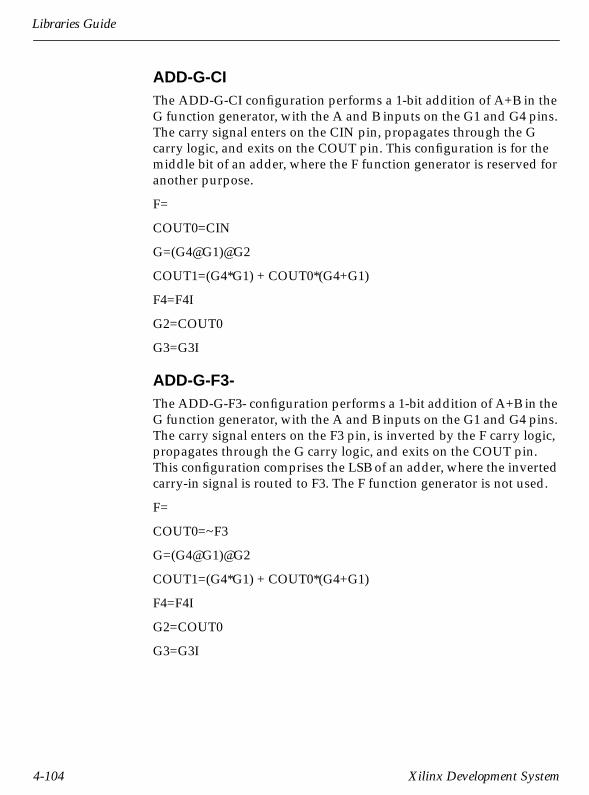
Libraries Guide
ADD-G-CIThe ADD-G-CI configuration performs a 1-bit addition of A+B in theG function generator, with the A and B inputs on the G1 and G4 pins.The carry signal enters on the CIN pin, propagates through the Gcarry logic, and exits on the COUT pin. This configuration is for themiddle bit of an adder, where the F function generator is reserved foranother purpose.
F=
COUT0=CIN
G=(G4@G1)@G2
COUT1=(G4*G1) + COUT0*(G4+G1)
F4=F4I
G2=COUT0
G3=G3I
ADD-G-F3-The ADD-G-F3- configuration performs a 1-bit addition of A+B in theG function generator, with the A and B inputs on the G1 and G4 pins.The carry signal enters on the F3 pin, is inverted by the F carry logic,propagates through the G carry logic, and exits on the COUT pin.This configuration comprises the LSB of an adder, where the invertedcarry-in signal is routed to F3. The F function generator is not used.
F=
COUT0=~F3
G=(G4@G1)@G2
COUT1=(G4*G1) + COUT0*(G4+G1)
F4=F4I
G2=COUT0
G3=G3I
4-104 Xilinx Development System

Attributes, Constraints, and Carry Logic
SUB-F-CIThe SUB-F-CI configuration performs a 1-bit twos-complementsubtraction of A-B in the F function generator, with the A input on F1and the B input on F2. The carry signal enters on the CIN pin, propa-gates through the F carry logic, and exits on the COUT pin. Thisconfiguration can be used as the MSB of a subtracter, with the G func-tion generator accessing the carry-out signal or calculating a twos-complement overflow.
F=(F1@F2)@~F4=~(F1@F2@F4)
COUT0=(F1*~F2) + CIN*(F1+~F2)
G=
COUT1=COUT0
F4=CIN
G2=G2I (COUT0 for overflow, OFL=G2@G3, or for carry-out,CO=G2)
G3=G3I (CIN for overflow, OFL=G2@G3)
SUB-FG-CIThe SUB-FG-CI configuration performs a 2-bit twos-complementsubtraction of A-B in both the F and G function generators. For thelower bit, the A input is on F1 and the B input is on F2. For the upperbit, the A input is on G4 and the B input is on G1. The carry signalenters on the CIN pin, propagates through the F and G carry logic,and exits on the COUT pin. This configuration comprises the middlebits of a subtracter.
F=(F1@F2)@~F4=~(F1@F2@F4)
COUT0=(F1*~F2) + CIN*(F1+~F2)
G=(G4@G1)@~G2=~(G4@G1@G2)
COUT1=(G4*~G1) +COUT0*(G4+~G1)
F4=CIN
G2=COUT0
G3=G3I
Libraries Guide 4-105

Libraries Guide
SUB-G-1The SUB-G-1 configuration performs a 1-bit twos-complementsubtraction of A-B in the G function generator, with the A input onG4 and the B input on G1. The carry-in is tied High (no borrow). Thecarry signal propagates through the G carry logic and exits on theCOUT pin. This configuration comprises the LSB of a subtracter withno carry-in. The F function generator is not used.
F=
COUT0=1
G=(G4@G1)
COUT1=(G4+~G1)
F4=F4I
G2=G2I
G3=G3I
SUB-G-F1The SUB-G-F1 configuration performs a 1-bit twos-complementsubtraction of A-B in the G function generator, with the A input onG4 and the B input on G1. The carry signal enters on the F1 pin, prop-agates through the G carry logic, and exits on the COUT pin. Thisconfiguration comprises the LSB of a subtracter, where the carry-insignal is routed to F1. The F function generator is not used.
F=
COUT0=F1
G=(G4@G1)@~G2=~(G4@G1@G2)
COUT1=(G4*~G1) + COUT0*(G4+~G1)
F4=F4I
G2=COUT0
G3=G3I
4-106 Xilinx Development System
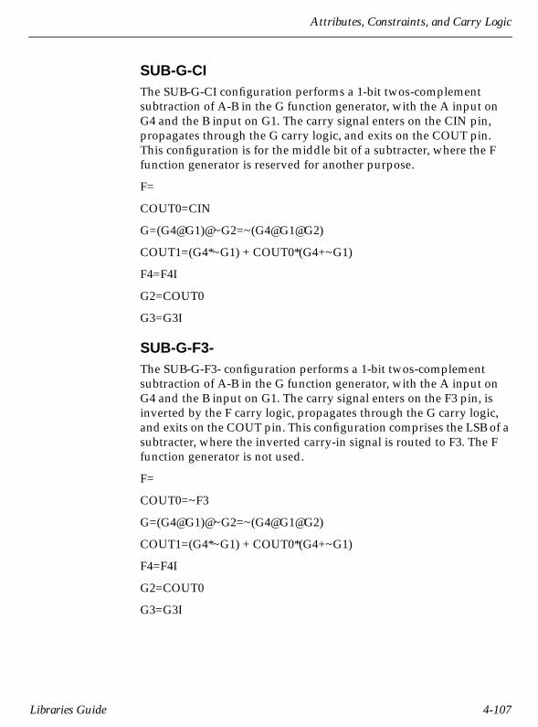
Attributes, Constraints, and Carry Logic
SUB-G-CIThe SUB-G-CI configuration performs a 1-bit twos-complementsubtraction of A-B in the G function generator, with the A input onG4 and the B input on G1. The carry signal enters on the CIN pin,propagates through the G carry logic, and exits on the COUT pin.This configuration is for the middle bit of a subtracter, where the Ffunction generator is reserved for another purpose.
F=
COUT0=CIN
G=(G4@G1)@~G2=~(G4@G1@G2)
COUT1=(G4*~G1) + COUT0*(G4+~G1)
F4=F4I
G2=COUT0
G3=G3I
SUB-G-F3-The SUB-G-F3- configuration performs a 1-bit twos-complementsubtraction of A-B in the G function generator, with the A input onG4 and the B input on G1. The carry signal enters on the F3 pin, isinverted by the F carry logic, propagates through the G carry logic,and exits on the COUT pin. This configuration comprises the LSB of asubtracter, where the inverted carry-in signal is routed to F3. The Ffunction generator is not used.
F=
COUT0=~F3
G=(G4@G1)@~G2=~(G4@G1@G2)
COUT1=(G4*~G1) + COUT0*(G4+~G1)
F4=F4I
G2=COUT0
G3=G3I
Libraries Guide 4-107

Libraries Guide
ADDSUB-F-CIThe ADDSUB-F-C1 configuration performs a 1-bit twos-complementadd/subtract of A+B in the F function generator, with the A input onF1 and the B input on F2. The carry signal enters on the CIN pin,propagates through the F carry logic, and exits on the COUT pin. TheF3 input indicates add (F3=1) or subtract (F3=0). This configurationcan be used as the MSB of an adder/subtracter, with the G functiongenerator accessing the carry-out signal or calculating a twos-comple-ment overflow.
F=(F1@F2)@F4@~F3=~(F1@F2@F4@F3)
COUT0=F3*((F1*F2) + CIN*(F1+F2)) + ~F3*((F1*~F2) +CIN*(F1+~F2))
G=
COUT1=COUT0
F4=CIN
G2=G2I (COUT0 for overflow, OFL=G2@G3, or for carry-out,CO=G2)
G3=G3I (CIN for overflow, OFL=G2@G3)
ADDSUB-FG-CIThe ADDSUB-FG-CI configuration performs a 2-bit twos- comple-ment add/subtract of A+B in both the F and G function generators.For the lower bit, the A input is on F1 and the B input is on F2. For theupper bit, the A input is on G4 and the B input is on G1. The carrysignal enters on the CIN pin, propagates through the F and G carrylogic, and exits on the COUT pin. The F3 and G3 inputs indicate add(F3=G3=1) or subtract (F3=G3=0): the add/subtract control signalmust be routed to both the F3 and G3 pins. This configurationcomprises the middle bits of an adder/subtracter.
F=(F1@F2)@F4@~F3=~(F1@F2@F4@F3)
COUT0=F3*((F1*F2) + CIN*(F1+F2)) + ~F3*((F1*~F2) +CIN*(F1+~F2))
G=(G4@G1)@G2@~G3=~(G4@G1@G2@G3)
4-108 Xilinx Development System

Attributes, Constraints, and Carry Logic
COUT1=F3*((G4*G1)+COUT0*(G4+G1))+~F3*((G4*~G1)+COUT0*(G4+~G1))
F4=CIN
G2=COUT0
G3=G3I
ADDSUB-G-F1The ADDSUB-G-F1 configuration performs a 1-bit twos-complementadd/subtract of A+B in the G function generator, with the A input onG4 and the B input on G1. The carry signal enters on the F1 pin, prop-agates through the G carry logic, and exits on the COUT pin. The F3and G3 inputs indicate add (F3=G3=1) or subtract (F3=G3=0): theadd/subtract control signal must be routed to both the F3 and G3pins. This configuration comprises the LSB of an adder/subtracter,where the carry-in signal is routed to F1. The F function generator isnot used.
F=
COUT0=F1
G=(G4@G1)@G2@~G3=~(G4@G1@G2@G3)
COUT1=F3*((G4*G1)+COUT0*(G4+G1))+~F3*((G4*~G1)+COUT0*(G4+~G1))
F4=F4I
G2=COUT0
G3=G3I
Libraries Guide 4-109

Libraries Guide
ADDSUB-G-CIThe ADDSUB-G-CI configuration performs a 1-bit twos-complementadd/subtract of A+B in the G function generator, with the A input onG4 and the B input on G1. The carry signal enters on the CIN pin,propagates through the G carry logic, and exits on the COUT pin. TheF3 and G3 inputs indicate add (F3=G3=1) or subtract (F3=G3=0): theadd/subtract control signal must be routed to both the F3 and G3pins. This configuration is for the middle bit of an adder/subtracter,where the F function generator is reserved for another purpose.
F=
COUT0=CIN
G=(G4@G1)@G2@~G3=~(G4@G1@G2@G3)
COUT1=F3*((G4*G1)+COUT0*(G4+G1))+~F3*((G4*~G1)+COUT0*(G4+~G1))
F4=F4I
G2=COUT0
G3=G3I
ADDSUB-G-F3-The ADDSUB-G-F3 configuration performs a 1-bit twos-complementadd/subtract of A+B in the G function generator, with the A input onG4 and the B input on G1. The carry signal enters on the F3 pin, isinverted by the F carry logic, propagates through the G carry logic,and exits on the COUT pin. Because the F3 input also indicates add(F3=1) or subtract (F3=0), the carry-in is always null (0 for add, 1 forsubtract). This configuration comprises the LSB of an adder/subtracter with no carry-in. The F function generator is not used.
F=
COUT0=~F3
G=(G4@G1)
COUT1=F3*G4*G1 + ~F3(G4+~G1)
F4=F4I
G2=COUT0
G3=G3I
4-110 Xilinx Development System

Attributes, Constraints, and Carry Logic
INC-F-CIThe INC-F-CI configuration performs a 1-bit increment in the F func-tion generator, with the input on the F1 pin. The carry signal enterson the CIN pin, propagates through the F carry logic, and exits on theCOUT pin. The G function generator can be used to output theterminal count of a counter.
F=(F1@F4)
COUT0=CIN*F1
G=
COUT1=COUT0
F4=CIN
G2=G2I (COUT0 for terminal count, TC=G2)
G3=G31
INC-FG-CIThe INC-FG-CI configuration performs a 2-bit increment in both theF and G function generators, with the lower-order input on the F1 pinand the higher-order input on the G4 pin. The carry signal enters onthe CIN pin, propagates through the F and G carry logic, and exits onthe COUT pin. This configuration comprises the middle bits of anincrementer.
F=(F1@F4)
COUT0=CIN*F1
G=(G4@G2)
COUT1=COUT0*G4
F4=CIN
G2=COUT0
G3=G3I
Libraries Guide 4-111
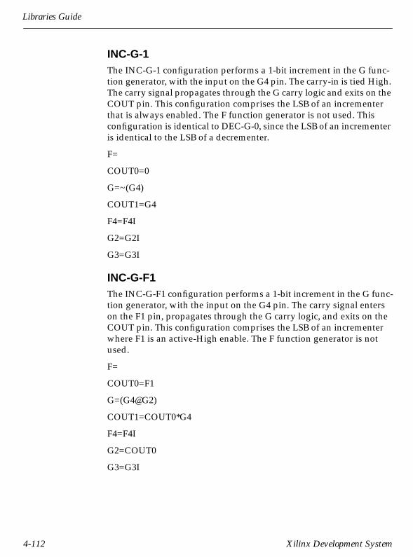
Libraries Guide
INC-G-1The INC-G-1 configuration performs a 1-bit increment in the G func-tion generator, with the input on the G4 pin. The carry-in is tied High.The carry signal propagates through the G carry logic and exits on theCOUT pin. This configuration comprises the LSB of an incrementerthat is always enabled. The F function generator is not used. Thisconfiguration is identical to DEC-G-0, since the LSB of an incrementeris identical to the LSB of a decrementer.
F=
COUT0=0
G=~(G4)
COUT1=G4
F4=F4I
G2=G2I
G3=G3I
INC-G-F1The INC-G-F1 configuration performs a 1-bit increment in the G func-tion generator, with the input on the G4 pin. The carry signal enterson the F1 pin, propagates through the G carry logic, and exits on theCOUT pin. This configuration comprises the LSB of an incrementerwhere F1 is an active-High enable. The F function generator is notused.
F=
COUT0=F1
G=(G4@G2)
COUT1=COUT0*G4
F4=F4I
G2=COUT0
G3=G3I
4-112 Xilinx Development System
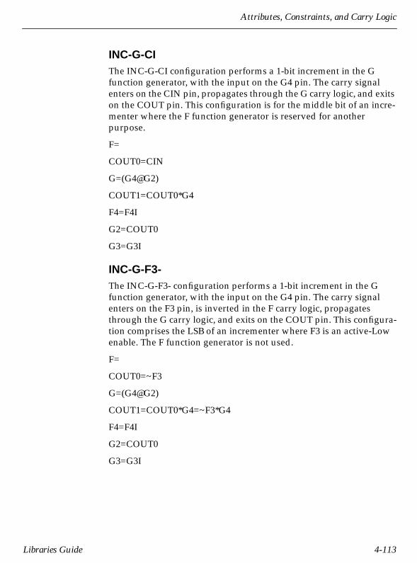
Attributes, Constraints, and Carry Logic
INC-G-CIThe INC-G-CI configuration performs a 1-bit increment in the Gfunction generator, with the input on the G4 pin. The carry signalenters on the CIN pin, propagates through the G carry logic, and exitson the COUT pin. This configuration is for the middle bit of an incre-menter where the F function generator is reserved for anotherpurpose.
F=
COUT0=CIN
G=(G4@G2)
COUT1=COUT0*G4
F4=F4I
G2=COUT0
G3=G3I
INC-G-F3-The INC-G-F3- configuration performs a 1-bit increment in the Gfunction generator, with the input on the G4 pin. The carry signalenters on the F3 pin, is inverted in the F carry logic, propagatesthrough the G carry logic, and exits on the COUT pin. This configura-tion comprises the LSB of an incrementer where F3 is an active-Lowenable. The F function generator is not used.
F=
COUT0=~F3
G=(G4@G2)
COUT1=COUT0*G4=~F3*G4
F4=F4I
G2=COUT0
G3=G3I
Libraries Guide 4-113

Libraries Guide
INC-FG-1The INC-FG-1 configuration performs a 2-bit increment in both the Fand G function generator, with the lower-order A input on the F1 pinand the higher-order A input on the G4 pin. The carry-in is tied High.The carry signal propagates through the F and G carry logic and exitson the COUT pin. This configuration comprises the two least signifi-cant bits of an incrementer that is always enabled.
F=~(F1)
COUT0=F1
G=G2@G4
COUT1=COUT0*G4
F4=F4I or CIN
G2=COUT0
G3=G3I or CIN
DEC-F-CIThe DEC-F-CI configuration performs a 1-bit decrement in the F func-tion generator, with the input on the F1 pin. The carry signal enterson the CIN pin, propagates through the F carry logic, and exits on theCOUT pin. The G function generator can be used to output theterminal count of a counter.
F=~(F1@F4)
COUT0=F1+CIN*~F1
G=
COUT1=COUT0
F4=CIN
G2=G2I (COUT0 for terminal count, TC=G2)
G3=G31
4-114 Xilinx Development System
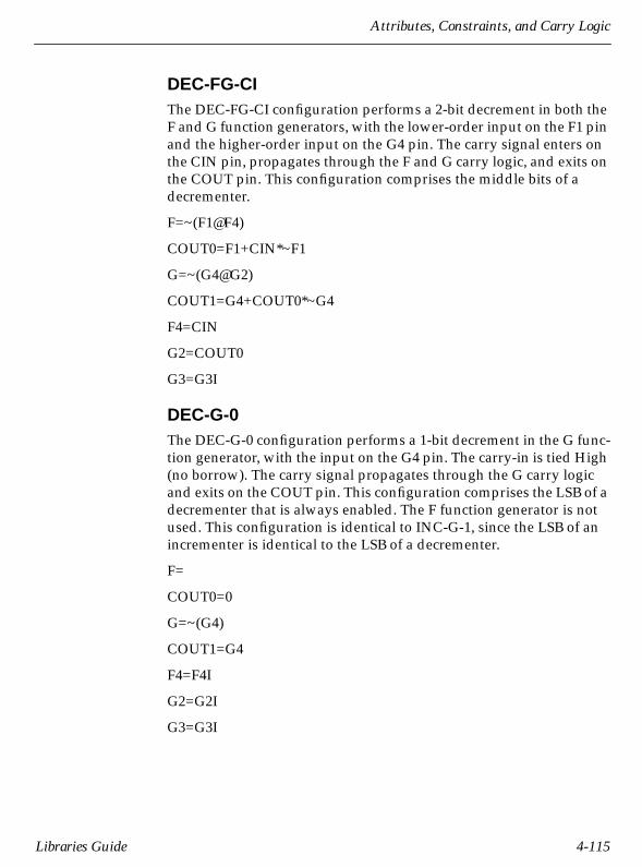
Attributes, Constraints, and Carry Logic
DEC-FG-CIThe DEC-FG-CI configuration performs a 2-bit decrement in both theF and G function generators, with the lower-order input on the F1 pinand the higher-order input on the G4 pin. The carry signal enters onthe CIN pin, propagates through the F and G carry logic, and exits onthe COUT pin. This configuration comprises the middle bits of adecrementer.
F=~(F1@F4)
COUT0=F1+CIN*~F1
G=~(G4@G2)
COUT1=G4+COUT0*~G4
F4=CIN
G2=COUT0
G3=G3I
DEC-G-0The DEC-G-0 configuration performs a 1-bit decrement in the G func-tion generator, with the input on the G4 pin. The carry-in is tied High(no borrow). The carry signal propagates through the G carry logicand exits on the COUT pin. This configuration comprises the LSB of adecrementer that is always enabled. The F function generator is notused. This configuration is identical to INC-G-1, since the LSB of anincrementer is identical to the LSB of a decrementer.
F=
COUT0=0
G=~(G4)
COUT1=G4
F4=F4I
G2=G2I
G3=G3I
Libraries Guide 4-115

Libraries Guide
DEC-G-F1The DEC-G-F1 configuration performs a 1-bit decrement in the Gfunction generator, with the input on the G4 pin. The carry signalenters on the F1 pin, propagates through the G carry logic, and exitson the COUT pin. This configuration comprises the LSB of a decre-menter where F1 is an active-Low enable. The F function generator isnot used.
F=
COUT0=F1
G=~(G4@G2)
COUT1=COUT0 + G4
F4=F4I
G2=COUT0
G3=G3I
DEC-G-CIThe DEC-G-CI configuration performs a 1-bit decrement in the Gfunction generator, with the input on the G4 pin. The carry signalenters on the CIN pin, propagates through the G carry logic, and exitson the COUT pin. This configuration is for the middle bit of a decre-menter, where the F function generator is reserved for anotherpurpose.
F=
COUT0=CIN
G=~(G4@G2)
COUT1=G4+COUT0*~G4
F4=F4I
G2=COUT0
G3=G3I
4-116 Xilinx Development System

Attributes, Constraints, and Carry Logic
DEC-G-F3-The DEC-G-F3- configuration performs a 1-bit decrement in the Gfunction generator, with the input on the G4 pin. The carry signalenters on the F3 pin, is inverted in the F carry logic, propagatesthrough the G carry logic, and exits on the COUT pin. This configura-tion comprises the LSB of a decrementer, where F3 is an active-Highenable. The F function generator is not used.
F=
COUT0=~F3
G=~(G4@G2)
COUT1=COUT0 + G4
F4=F4I
G2=COUT0
G3=G3I
DEC-FG-0The DEC-FG-0 configuration performs a 2-bit decrement in both the Fand G function generator, with the lower-order input on the F1 pinand the higher order input on the G4 pin. The carry-in is tied Low.The carry signal propagates through the F and G carry logic and exitson the COUT pin. This configuration comprises the two least signifi-cant bits of a decrementer that is always enabled.
F=~(F1)
COUT0=F1
G=~(G4@G2)
COUT=COUT1=(COUT0*~G4) + G4
F4=F4I
G2=COUT0
G3=G3I
Libraries Guide 4-117

Libraries Guide
INCDEC-F-CIThe INCDEC-F-CI configuration performs a 1-bit increment/decre-ment in the F function generator, with the input on the F1 pin. Thecarry signal enters on the CIN pin, propagates through the F carrylogic, and exits on the COUT pin. The F3 input indicates increment(F3=1) or decrement (F3=0). The G function generator can be used tooutput the terminal count of a counter.
F=(F1@F4)@~F3
COUT0=~F3*(F1+ CIN) + F3*F1*CIN
G=
COUT1=COUT0
F4=CIN
G2=G2I (COUT0 for terminal count, TC=G2)
G3=G31
INCDEC-FG-CIThe INCDEC-FG-CI configuration performs a 2-bit increment/decre-ment in both the F and G function generators, with the lower-orderinput on the F1 pin and the higher-order input on the G4 pin. Thecarry signal enters on the CIN pin, propagates through the F and Gcarry logic, and exits on the COUT pin. The F3 and G3 inputs indicateincrement (F3=G3=1) or decrement (F3=G3=0): the increment/decre-ment control signal must be routed to both the F3 and G3 pins. Thisconfiguration comprises the middle bits of an incrementer/decre-menter.
F=(F1@F4)@~F3
COUT0=~F3*(F1+ CIN) + F3*F1*CIN
G=(G4@G2)@~G3
COUT1=~F3*(G4+ COUT0) + F3*G4*COUT0
F4=CIN
G2=COUT0
G3=G3I
4-118 Xilinx Development System

Attributes, Constraints, and Carry Logic
INCDEC-G-0The INCDEC-G-0 configuration performs a 1-bit increment/decre-ment in the G function generator, with the input on the G4 pin. Thecarry-in is tied High. The carry signal propagates through the G carrylogic and exits on the COUT pin. This configuration comprises theLSB of an incrementer/decrementer that is always enabled. The Ffunction generator is not used. F3 is not required for increment/decrement control, since the LSB of an incrementer is identical to theLSB of a decrementer; this configuration is identical to INC-G-1 andDEC-G-0.
F=
COUT0=0
G=~(G4)
COUT1=G4
F4=F4I
G2=G2I
G3=G3I
INCDEC-G-F1The INCDEC-G-F1 configuration performs a 1-bit increment/decre-ment in the G function generator, with the input on the G4 pin. Thecarry signal enters on the F1 pin, propagates through the G carrylogic, and exits on the COUT pin. This configuration comprises theLSB of an incrementer/decrementer where the carry-in signal isrouted to F1. The carry-in is active-High for an increment operationand active-Low for a decrement operation. The F function generatoris not used. The F3 and G3 inputs indicate increment (F3=G3=1) ordecrement (F3=G3=0): the increment/decrement control signal mustbe routed to both the F3 and G3 pins.
F=
COUT0=F1
G=(G4@G2)@~G3
COUT1=F3*(G4*COUT0) + ~F3*(G4+COUT0)
F4=F4I
G2=COUT0
G3=G3I
Libraries Guide 4-119

Libraries Guide
4-120 Xilinx Development System
INCDEC-G-CIThe INCDEC-G-CI configuration performs a 1-bit increment/decre-ment in the G function generator, with the input on the G4 pin. Thecarry signal enters on the CIN pin, propagates through the G carrylogic, and exits on the COUT pin. The F3 and G3 inputs indicateincrement (F3=G3=1) or decrement (F3=G3=0): the increment/decre-ment control signal must be routed to both the F3 and G3 pins. Thisconfiguration is for the middle bit of an incrementer/decrementer,where the F function generator is reserved for another purpose,although the F3 pin is used by the carry logic.
F=
COUT0=CIN
G=(G4@G2)@~G3
COUT1=~F3*(G4+ COUT0) + F3*G4*COUT0
F4=F4I
G2=COUT0
G3=G3I
INCDEC-FG-1The INCDEC-FG-1 configuration performs a 2-bit increment/decre-ment in both the F and G function generator, with the lower- orderinput on the F1 pin and the higher-order input on the G4 pin. The F3and G3 inputs indicate increment (F3=G3=1) or decrement(F3=G3=0): the increment/decrement control signal must be routedto both the F3 and G3 pins. The carry-in is always active (High inincrement mode and Low in decrement mode). The carry signal prop-agates through the F and G carry logic and exits on the COUT pin.This configuration comprises the two least significant bits of an incre-menter/decrementer that is always enabled.
F=~(F1)
COUT0=F1
G=(G2@G4)@~G3
COUT=COUT1=~F3*((COUT0*~G4)+G4) + F3*(G4*COUT0)
F4=F4I
G2=COUT0
G3=G3I

Attributes, Constraints, and Carry Logic
FORCE-0The FORCE-0 configuration forces the carry-out signal on the COUTpin to be 0.
COUT0=0
COUT1=0
FORCE-1The FORCE-1 configuration forces the carry-out signal on the COUTpin to be 1.
COUT0=1
COUT1=1
FORCE-F1The FORCE-F1 configuration forces the signal on the F1 pin to passthrough to the COUT pin.
COUT0=F1
COUT1=COUT0=F1
FORCE-CIThe FORCE-CI configuration forces the signal on the CIN pin to passthrough to the COUT pin.
COUT0=CIN
COUT1=COUT0=CIN
FORCE-F3-The FORCE-F3- configuration forces the signal on the F3 pin to passinverted to the COUT pin.
COUT0=~F3
COUT1=COUT0=~F3
Libraries Guide 4-121

Libraries Guide
EXAMINE-CIThe EXAMINE-CI configuration allows the carry signal on the CINpin to be used in the F or G function generators. This configurationforces the signal on the CIN pin to pass through to the COUT pin andis equivalent to the FORCE-CI configuration. EXAMINE-CI isprovided for CLBs in which the carry logic is unused but the CINsignal is required.
COUT0=CIN
COUT1=COUT0=CIN
4-122 Xilinx Development System

Index
AACC, 4-33ACLK, 4-19, 4-27
BPAD, 4-5BUFE, 4-15BUFGP, 4-19, 4-27, 4-54, 4-70, 4-71
Libraries Guide — 0401410 01 i
ADD, 4-33ADD-F-CI, 4-102ADD-FG-CI, 4-103ADD-G-CI, 4-104ADD-G-F1, 4-103ADD-G-F3-, 4-104ADDSUB-F-C1, 4-108ADDSUB-FG-CI, 4-108ADDSUB-G-CI, 4-110ADDSUB-G-F1, 4-109ADDSUB-G-F3, 4-110ADSU, 4-33APR, 4-34
BBASE attribute
architectures, 4-2purpose, 4-2syntax, 4-4XC2000 modes, 4-2XC3000 modes, 4-2
BLKNM attribute, 4-4, 4-47architectures, 4-4Place Block constraint, 4-49purpose, 4-4symbols, 4-5syntax, 4-6, 4-46
Boolean minimization, 4-31Boolean operators
XC2000, 4-12XC3000, 4-12
BUFGS, 4-19, 4-27, 4-54, 4-70BUFT, 4-20, 4-67
constraints, 4-67LOC placement examples, 4-26placement constraint syntax, 4-52, 4-54use with BLKNM attribute, 4-5use with DECODE attribute, 4-11use with DOUBLE attribute, 4-12use with HBLKNM attribute, 4-16use with LOC constraint, 4-19, 4-21, 4-72use with net attributes, 4-33use with RLOC constraint, 4-40, 4-72use with RLOC_ORIGIN constraint, 4-41, 4-86use with RLOC_RANGE constraint, 4-89
bus pad symbols, 4-21
CC net attribute, 4-33CAP attribute
architectures, 4-6purpose, 4-6symbols, 4-6syntax, 4-7
capacitive mode, 4-6, 4-40carry logic, 4-96, 4-97
carry mode configuration mnemonics,4-101carry mode names and symbols, 4-99
Libraries Guide
carry mode primitive symbols, 4-98handling in XNFPrep, 4-100LOC constraints, 4-99primitives, 4-98RLOC constraints, 4-99
carry mode configuration mnemonics, 4-101carry mode names and symbols, 4-99carry mode primitive symbols, 4-98CIN pin, 4-100, 4-101CIN pin see also individual carry mode con-figuration mnemonicsCLBMAP, 4-20, 4-59
closed, 4-62locked pins, 4-62mapping constraints, 4-61open, 4-62unlocked pins, 4-62use with BLKNM attribute, 4-5use with HBLKNM attribute, 4-16use with LOC constraint, 4-19use with MAP attribute, 4-29use with net attributes, 4-34use with Place Block constraint, 4-49
CLBMAP constraints, 4-61CLBs, 4-55
aligning inputs with longline, 4-34base configuration, 4-2block definition, 4-47CLBMAP constraints, 4-61clocks, 4-33combinational logic, 4-35constraints, 4-63dedicated carry logic, 4-98, 4-101flip-flop constraints, 4-55LOC constraint examples, 4-24mapping gates into function generators,4-46mapping with BLKNM attribute, 4-5pin swapping, 4-29Place Block constraint, 4-49
prohibiting logic placement, 4-21ROM and RAM constraints, 4-57setting logic equations for functiongenerators, 4-12specifying functions with CONFIGattribute, 4-8symbols, 4-16, 4-20use with BLKNM attribute, 4-5use with LOC constraint, 4-19, 4-21, 4-72use with RLOC constraint, 4-73XC2000 configuration options, 4-9XC3000 configuration options, 4-10
clock buffers, 4-19CLOCK_OPT attribute
architectures, 4-7purpose, 4-7syntax, 4-7
CMOS attributearchitectures, 4-8output drive levels, 4-8purpose, 4-8symbols, 4-8syntax, 4-8
COMPM, 4-33CONFIG attribute
architectures, 4-8purpose, 4-8symbols, 4-8syntax, 4-9XC2000 CLB configuration options, 4-9XC2000 IOB configuration options, 4-9XC3000 CLB configuration options, 4-10XC3000 IOB configuration options, 4-10
constraints file see CST file, 4-46COUT pin, 4-100COUT pin see also individual carry modeconfiguration mnemonicsCOUT0 pin, 4-100, 4-102COUT1 pin, 4-102
ii Xilinx Development System
Index
CST file, 4-46BUFT constraints, 4-67CLB constraints, 4-63CLBMAP constraints, 4-61edge decoder constraints, 4-69flag constraints, 4-52flip-flop constraints, 4-55FMAP constraints, 4-59global buffer constraints, 4-70HMAP constraints, 4-59I/O constraints, 4-64IOB constraints, 4-67Notplace Block constraints, 4-49Notplace Instance constraints, 4-48, 4-54, 4-63, 4-67Place Block constraints, 4-49place constraints, 4-51Place Instance constraints, 4-48, 4-55PPR, 4-55, 4-67RAM constraints, 4-57restrictions, 4-54ROM constraints, 4-57symbol names, 4-54syntactical conventions, 4-50TIMEGRP constraints, 4-54TIMESPEC constraints, 4-52weight constraints, 4-52wildcards, 4-50, 4-66
CY4 symbols, 4-72, 4-99, 4-100
DDEC-F-CI, 4-114DEC-FG-0, 4-117DEC-FG-CI, 4-115DEC-G-0, 4-115DEC-G-CI, 4-116DEC-G-F1, 4-116DEC-G-F3-, 4-117DECODE attribute, 4-69
architectures, 4-11purpose, 4-11symbols, 4-11
syntax, 4-11decode logic, 4-28DECODE macro, 4-69DECODEn symbols, 4-20decoders, 4-72dedicated carry logic, 4-98design, 4-94design hierarchy, 4-16, 4-17, 4-45, 4-75, 4-76, 4-78, 4-79, 4-80, 4-82, 4-92DFF, 4-72DOUBLE attribute
architectures, 4-11purpose, 4-11symbols, 4-12syntax, 4-12
Eedge decoders, 4-11, 4-46
constraints, 4-69edge designations, 4-69
EditLCA, 4-6, 4-26, 4-65EQUATE_F attribute
architectures, 4-12purpose, 4-12syntax, 4-12
EQUATE_G attributearchitectures, 4-12purpose, 4-12syntax, 4-12
EXAMINE-CI, 4-100, 4-122EXT record, 4-64
FF mode, 4-2F net attribute, 4-33FAST attribute
architectures, 4-13purpose, 4-13symbols, 4-13syntax, 4-13
fast function blocks, 4-33, 4-38FastCLK, 4-39
Libraries Guide iii
Libraries Guide
optimization, 4-7FastInput path, 4-33FD registers, 4-39FDCE, 4-5, 4-72FDCP, 4-5, 4-33FDCPE, 4-33FDPE, 4-5, 4-72FFB, 4-33FG mode, 4-2FGM mode, 4-2FILE attribute
architectures, 4-13example, 4-14purpose, 4-13syntax, 4-14
FITNET command, 4-37flag constraints, 4-52flip-flops, 4-5
clock pins, 4-33constraints, 4-55CST file, 4-55IOB, 4-35macros, 4-93Q output, 4-2use with BLKNM attribute, 4-5use with FAST attribute, 4-13use with LOC constraint, 4-19, 4-24, 4-55use with RLOC constraint, 4-73, 4-78, 4-81X, 4-25XC3000A/L, 4-55XC4000 primitives, 4-5Y, 4-25
FMAPmapping constraints, 4-59placement constraints, 4-46relationally placed macros, 4-96schematics example, 4-60Unified Libraries, 4-72use with BLKNM attribute, 4-5
use with HBLKNM attribute, 4-16use with LOC constraint, 4-19, 4-20use with MAP attribute, 4-29use with net attributes, 4-34use with Place Block constraint, 4-49use with RLOC constraint, 4-72
FMAP constraints, 4-59FOE, 4-15, 4-33FOE_OPT attribute
architectures, 4-15purpose, 4-15syntax, 4-15
FORCE-0, 4-121FORCE-1, 4-121FORCE-CI, 4-121FORCE-F1, 4-121FORCE-F3-, 4-121function generators, 4-101
base configuration modes, 4-2carry logic, 4-98carry mode configuration syntax, 4-101grouping with BLKNM attribute, 4-5grouping with HBLKNM attribute, 4-16logic equations for F and G, 4-12, 4-102mapping constraints, 4-59mapping into F, 4-59mapping into H, 4-59merging with MAP attribute, 4-30placement constraints, 4-46specifying with LOC constraint, 4-24
function generators see also individual car-ry mode configuration mnemonics
GG net attribute, 4-33GCLK, 4-19, 4-27global buffers, 4-46
constraints, 4-70corner designations, 4-70LOC placement examples, 4-27
ground bounce, 4-6, 4-39
iv Xilinx Development System

Index
HH net attribute, 4-33H_SET constraint, 4-17, 4-76, 4-77, 4-87, 4-95HBLKNM attribute, 4-47
architectures, 4-16purpose, 4-16symbols, 4-16syntax, 4-17, 4-46
hierarchical design see design hierarchy, 4-16high-density function blocks, 4-33, 4-38HM2RPM utility, 4-96HMAP
mapping constraints, 4-59placement constraints, 4-46relationally placed macros, 4-96schematics example, 4-60Unified Libraries, 4-72use with BLKNM attribute, 4-5use with HBLKNM attribute, 4-16use with LOC constraint, 4-19, 4-20use with MAP attribute, 4-29use with net attributes, 4-34use with Place Block constraint, 4-49use with RLOC constraint, 4-72
HMAP constraints, 4-59horizontal longline, 4-11, 4-20, 4-69HU_SET constraint, 4-87, 4-95
architectures, 4-17purpose, 4-17purppose, 4-82syntax, 4-18, 4-82
II net attribute, 4-34I/O block primitives, 4-5, 4-16, 4-19I/O buffers, 4-5, 4-16, 4-25, 4-36I/O constraints, 4-64I/O pads, 4-25, 4-46I/O pins, 4-21, 4-36
I/O primitives, 4-34, 4-72I/O registers, 4-25I/O symbols, 4-31, 4-35, 4-40IBUF, 4-5, 4-8, 4-19, 4-33, 4-39, 4-44IFD, 4-5, 4-8, 4-44Ignore_xnf_locs option, 4-20ILD, 4-5, 4-8, 4-44INCDEC-F-CI, 4-118INCDEC-FG-1, 4-120INCDEC-FG-CI, 4-118INCDEC-G-0, 4-119INCDEC-G-CI, 4-120INCDEC-G-F1, 4-119INC-F-CI, 4-111INC-FG-1, 4-114INC-FG-CI, 4-111INC-G-1, 4-112INC-G-CI, 4-113INC-G-F1, 4-112INC-G-F3-, 4-113INFF, 4-8, 4-19, 4-44INIT attribute
architectures, 4-18purpose, 4-18syntax, 4-18
INLAT, 4-8, 4-44input buffers, 4-19input registers, 4-29, 4-38, 4-39input threshold levels, 4-8INREG, 4-8, 4-44IOBs, 4-67
base configuration, 4-2block definition, 4-47constraints, 4-54, 4-67edge designations, 4-65half-edge designations, 4-66I/O constraints, 4-64increasing output speed with FASTattribute, 4-13LOC constraint examples, 4-25Notplace Instance constraints, 4-67
Libraries Guide v

Libraries Guide
output symbols, 4-7pads, 4-7prohibiting logic placement, 4-21removing default delay, 4-35specifying function with CONFIGattribute, 4-8symbols, 4-13, 4-19use with BLKNM attribute, 4-5use with global buffers, 4-71use with LOC constraint, 4-72XC2000 configuration options, 4-9XC3000 configuration options, 4-10
IOPAD, 4-7, 4-13, 4-20IPAD, 4-5, 4-20
KK net attribute, 4-34
LL net attribute, 4-34latch enable pins, 4-33, 4-34latches, 4-5, 4-16, 4-19, 4-35, 4-42LCA block names, 4-4, 4-49LD, 4-33LDCP, 4-5LOC constraint, 4-55, 4-57
architectures, 4-19area constraints, 4-23, 4-99BUFT placement examples, 4-26carry logic, 4-99CLB placement examples, 4-24decode logic placement examples, 4-28global buffer placement examples, 4-27global buffers, 4-70IOB placement examples, 4-25multiple constraints, 4-24prohibit constraints, 4-23, 4-99propagation through flattening, 4-94purpose for EPLDs, 4-20purpose for FPGAs, 4-19single constraints, 4-22, 4-99syntax, 4-46
syntax for EPLDs, 4-22syntax for FPGAs, 4-21
logic optimization, 4-36LOGIC_OPT attribute
architectures, 4-28purpose, 4-28syntax, 4-28
LOWPWR attributearchitectures, 4-29purpose, 4-29syntax, 4-29
LSB, 4-103, 4-104, 4-106, 4-107, 4-109, 4-110, 4-112, 4-113, 4-115, 4-116, 4-117, 4-119
Mmacro symbols, 4-93macrocells, 4-29, 4-33, 4-36, 4-39, 4-44MAP attribute, 4-62
architectures, 4-29purpose, 4-29syntax, 4-30
mapping control symbols, 4-5MEDFAST attribute
architectures, 4-31purpose, 4-31syntax, 4-31
MEDSLOW attributearchitectures, 4-31purpose, 4-31syntax, 4-31
MemGen, 4-57, 4-58Mentor, 4-2, 4-43MINIMIZE attribute
architectures, 4-31purpose, 4-31syntax, 4-32
MRINPUT attributearchitectures, 4-32purpose, 4-32syntax, 4-32
MSB, 4-102, 4-105, 4-108
vi Xilinx Development System

Index
NN net attribute, 4-34net attributes
architectures, 4-32C, 4-33F, 4-33G, 4-33H, 4-33I, 4-34K, 4-34L, 4-34N, 4-34P, 4-34purpose, 4-33S, 4-34syntax, 4-35W, 4-34X, 4-35
NODELAY attributearchitectures, 4-35purpose, 4-35syntax, 4-36
Notplace Block constraints, 4-49Notplace Instance constraints, 4-48, 4-54,4-63, 4-67
OOBUF, 4-5, 4-7, 4-8, 4-13, 4-15, 4-19, 4-44OBUFE, 4-15OBUFT, 4-5, 4-7, 4-8, 4-13, 4-44OFD, 4-5, 4-8, 4-13, 4-44OFDI, 4-13OFDT, 4-5, 4-8, 4-13, 4-44OFDTI, 4-13OPAD, 4-5, 4-7, 4-13, 4-20OPT attribute
architectures, 4-36purpose, 4-36syntax, 4-36
OUTFF, 4-8, 4-19, 4-44OUTFFT, 4-8, 4-44
output buffers, 4-19output drive levels, 4-8
PP net attribute, 4-34PAD, 4-5, 4-20pad names, 4-51PAD primitives, 4-5, 4-16pad registers, 4-39PAD symbols, 4-20, 4-64, 4-66pad symbols, 4-19, 4-21pads, 4-42PADU, 4-5pin grid arrays, 4-67PinSave command, 4-21Place Block constraints, 4-49place constraints, 4-51Place Instance constraints, 4-48, 4-55PLC, 4-30PLD attribute
architectures, 4-37purpose, 4-37syntax, 4-37
PLD equation file, 4-38PLFB9, 4-33PLO, 4-30, 4-59PLUSASM, 4-37, 4-38PPR
BUFT constraints, 4-67CLB constraints, 4-63edge decoder constraints, 4-69FMAP mapping, 4-59, 4-60global buffer constraints, 4-70HMAP mapping, 4-59, 4-60I/O constraints, 4-64Ignore_maps option, 4-59Ignore-xnf_locs option, 4-20IOB constraints, 4-67LOC constraints, 4-55, 4-57Place Block constraints, 4-49Place Instance constraints, 4-48placement constraints, 4-46
Libraries Guide vii
Libraries Guide
constraints file syntax, 4-47schematic syntax, 4-46
RLOC constraints, 4-71use with DOUBLE attribute, 4-12weight net attribute values, 4-34X net attribute, 4-35
PRELOAD_OPT attributearchitectures, 4-38purpose, 4-38syntax, 4-38
PRLD equations, 4-38properties, 4-2PUC, 4-30, 4-59pull-down transistors, 4-6, 4-40pull-up resistors, 4-11, 4-12, 4-20PULLUP symbols, 4-11, 4-20PUO, 4-30, 4-59
RRAM constraints, 4-57RAM16X1, 4-72RAM32X1, 4-72RAM64X8, 4-57, 4-58RAMs, 4-42REG_OPT attribute
architectures, 4-39purpose, 4-39syntax, 4-39
registers, 4-36, 4-38relationally placed macros, 4-71, 4-96RES attribute
architectures, 4-39purpose, 4-39syntax, 4-40
resistive mode, 4-6, 4-39RLOC constraint, 4-18
architectures, 4-40carry logic, 4-99propagation, 4-94purpose, 4-40, 4-71set linkage, 4-78
set modification, 4-80set modifiers, 4-85sets, 4-74, 4-94symbols, 4-72syntax, 4-40, 4-46, 4-72use with pre-Unified Librarieselements, 4-72use with Unified Libraries elements, 4-72use with Xilinx macros, 4-93
RLOC_ORIGIN constraint, 4-72, 4-91architectures, 4-41modifying H_SET, 4-87modifying HU_SET, 4-87purpose, 4-41, 4-86syntax, 4-41, 4-86
RLOC_RANGE constraintarchitectures, 4-42purpose, 4-42, 4-89syntax, 4-42, 4-90
ROM constraints, 4-57ROM16X1, 4-72ROM32X1, 4-72ROMs, 4-18RPMs, 4-71, 4-96
SS net attribute, 4-34soft macros, 4-19, 4-20, 4-24, 4-25, 4-96special function access symbols, 4-7, 4-13,4-31, 4-35, 4-40SUB-F-CI, 4-105SUB-FG-CI, 4-105SUB-G-1, 4-106SUB-G-CI, 4-107SUB-G-F1, 4-106SUB-G-F3-, 4-107synchronous reset, 4-102
TTCK, 4-7, 4-13, 4-31, 4-35, 4-40TDI, 4-7, 4-13, 4-31, 4-35, 4-40
viii Xilinx Development System

Index
three-state buffers, 4-5, 4-46three-state PLD outputs, 4-15TIMEGRP constraints, 4-54TIMESPEC constraints, 4-52TMS, 4-7, 4-13, 4-31, 4-35, 4-40TNM attribute
architectures, 4-42purpose, 4-42syntax, 4-43
Translate menu, 4-21TSidentifier attribute
architectures, 4-43purpose, 4-43syntax, 4-43
TTL attributearchitectures, 4-44purpose, 4-44syntax, 4-44
UU_SET constraint, 4-87, 4-94
architectures, 4-45purpose, 4-45, 4-75syntax, 4-46, 4-75use with USE_RLOC constraint, 4-92
UIM optimization, 4-44UIM_OPT attribute
architectures, 4-44purpose, 4-44syntax, 4-45
Unified Libraries, 4-72universal interconnect matrix (UIM), 4-7UPAD, 4-5, 4-7, 4-13, 4-20USE_RLOC constraint
architectures, 4-45purpose, 4-45, 4-90syntax, 4-45, 4-90using with U_SET, 4-92
user-created symbols, 4-19
VVHDL, 4-1VMF file, 4-21
WW net attribute, 4-34WAND, 4-19, 4-20, 4-54, 4-69, 4-70WAND1, 4-11weight constraints, 4-52wide-edge decoders, 4-11, 4-20wildcards, 4-25, 4-27, 4-42, 4-49, 4-50, 4-53,4-56, 4-58, 4-63, 4-64, 4-66, 4-68, 4-90, 4-99
XX net attribute, 4-35XC4000H output driver, 4-6XDE, 4-20, 4-35XEMake, 4-37Xilinx macros, 4-93XNF file, 4-13, 4-55, 4-57, 4-58, 4-64, 4-67,4-69, 4-70XNFMAP, 4-35, 4-47, 4-49, 4-61XNFMerge, 4-14, 4-15, 4-17, 4-19, 4-76, 4-77, 4-81, 4-82, 4-85, 4-86, 4-91, 4-93, 4-94XNFPrep, 4-20, 4-100, 4-101XOR7, 4-33XOR8, 4-33XOR9, 4-33XTF file, 4-55, 4-57, 4-64, 4-67, 4-69, 4-70
Libraries Guide ix

Libraries Guide
x Xilinx Development System

Trademark Information
Libraries Guide — 0401410 01
, XACT, XC2064, XC3090, XC4005, and XC-DS501 are registered trademarks ofXilinx. All XC-prefix product designations, XACT-Floorplanner, XACT-Performance,XAPP, XAM, X-BLOX, X-BLOX plus, XChecker, XDM, XDS, XEPLD, XPP, XSI, BITA,Configurable Logic Cell, CLC, Dual Block, FastCLK, HardWire, LCA, Logic Cell,LogicProfessor, MicroVia, PLUSASM, SMARTswitch, UIM, VectorMaze, VersaBlock,VersaRing, and ZERO+ are trademarks of Xilinx. The Programmable Logic Company andThe Programmable Gate Array Company are service marks of Xilinx.
IBM is a registered trademark and PC/AT, PC/XT, PS/2 and Micro Channel aretrademarks of International Business Machines Corporation. DASH, Data I/O andFutureNet are registered trademarks and ABEL, ABEL-HDL and ABEL-PLA aretrademarks of Data I/O Corporation. SimuCad and Silos are registered trademarks and P-Silos and P/C-Silos are trademarks of SimuCad Corporation. Microsoft is a registeredtrademark and MS-DOS is a trademark of Microsoft Corporation. Centronics is aregistered trademark of Centronics Data Computer Corporation. PAL and PALASM areregistered trademarks of Advanced Micro Devices, Inc. UNIX is a trademark of AT&TTechnologies, Inc. CUPL, PROLINK, and MAKEPRG are trademarks of Logical Devices,Inc. Apollo and AEGIS are registered trademarks of Hewlett-Packard Corporation.Mentor and IDEA are registered trademarks and NETED, Design Architect, QuickSim,QuickSim II, and EXPAND are trademarks of Mentor Graphics, Inc. Sun is a registeredtrademark of Sun Microsystems, Inc. SCHEMA II+ and SCHEMA III are trademarks ofOmation Corporation. OrCAD is a registered trademark of OrCAD Systems Corporation.Viewlogic, Viewsim, and Viewdraw are registered trademarks of Viewlogic Systems, Inc.CASE Technology is a trademark of CASE Technology, a division of the TeradyneElectronic Design Automation Group. DECstation is a trademark of Digital EquipmentCorporation. Synopsys is a registered trademark of Synopsys, Inc. Verilog is a registeredtrademark of Cadence Design Systems, Inc.
Xilinx does not assume any liability arising out of the application or use of any productdescribed or shown herein; nor does it convey any license under its patents, copyrights, ormaskwork rights or any rights of others. Xilinx reserves the right to make changes, at anytime, in order to improve reliability, function or design and to supply the best productpossible. Xilinx will not assume responsibility for the use of any circuitry described hereinother than circuitry entirely embodied in its products. Xilinx devices and products areprotected under one or more of the following U.S. Patents: 4,642,487; 4,695,740; 4,706,216;4,713,557; 4,746,822; 4,750,155; 4,758,985; 4,820,937; 4,821,233; 4,835,418; 4,853,626;
R
Trademark Information
4,855,619; 4,855,669; 4,902,910; 4,940,909; 4,967,107; 5,012,135; 5,023,606; 5,028,821;5,047,710; 5,068,603; 5,140,193; 5,148,390; 5,155,432; 5,166,858; 5,224,056; 5,243,238;5,245,277; 5,267,187; 5,291,079; 5,295,090; 5,302,866; 5,319,252; 5,319,254; 5,321,704;5,329,174; 5,329,181; 5,331,220; 5,331,226; 5,332,929; 5,337,255; 5,343,406; 5,349,248;5,349,249; 5,349,250; 5,349,691; 5,357,153; 5,360,747; 5,361,229; 5,362,999; 5,365,125;5,367,207; 5,386,154; 5,394,104; 5,399,924; 5,399,925; 5,410,189; 5,410,194; 5,414,377; RE34,363, RE 34,444, and RE 34,808. Other U.S. and foreign patents pending. Xilinx, Inc. doesnot represent that devices shown or products described herein are free from patentinfringement or from any other third party right. Xilinx assumes no obligation to correctany errors contained herein or to advise any user of this text of any correction if such bemade. Xilinx will not assume any liability for the accuracy or correctness of anyengineering or software support or assistance provided to a user.
Xilinx products are not intended for use in life support appliances, devices, or systems.Use of a Xilinx product in such applications without the written consent of theappropriate Xilinx officer is prohibited.
Xilinx Development System