gtl2003 8-bit bidirectional low voltage translator · 1. general description the gunning...
TRANSCRIPT

1. General description
The Gunning Transceiver Logic - Transceiver Voltage Clamps (GTL-TVC) provide high-speed voltage translation with low ON-state resistance and minimal propagation delay. The GTL2003 provides eight NMOS pass transistors (Sn and Dn) with a common gate (GREF) and a reference transistor (SREF and DREF). The device allows bidirectional voltage translations between 0.8 V and 5.0 V without use of a direction pin. Voltage translation below 0.8 V can be achieved when properly biased. For more information, refer to application note AN11127 (Ref. 1).
When the Sn or Dn port is LOW, the clamp is in the ON-state and a low resistance connection exists between the Sn and Dn ports. Assuming the higher voltage is on the Dn port, when the Dn port is HIGH, the voltage on the Sn port is limited to the voltage set by the reference transistor (SREF). When the Sn port is HIGH, the Dn port is pulled to VDD1 by the pull-up resistors. This functionality allows a seamless translation between higher and lower voltages selected by the user, without the need for directional control.
All transistors have the same electrical characteristics and there is minimal deviation from one output to another in voltage or propagation delay. This is a benefit over discrete transistor voltage translation solutions, since the fabrication of the transistors is symmetrical. Because all transistors in the device are identical, SREF and DREF can be located on any of the other eight matched Sn/Dn transistors, allowing for easier board layout. The translator's transistors provide excellent ESD protection to lower voltage devices and at the same time protect less ESD-resistant devices.
2. Features and benefits
8-bit bidirectional low voltage translator
Allows voltage level translation between 0.8 V, 0.9 V, 1.0 V, 1.2 V, 1.5 V, 1.8 V, 2.5 V, 3.3 V, and 5 V buses which allows direct interface with GTL, GTL+, LVTTL/TTL and 5 V CMOS levels
Provides bidirectional voltage translation with no direction pin
Low 6.5 ON-state resistance (Ron) between input and output pins (Sn/Dn)
Supports hot insertion
No power supply required: will not latch up
5 V tolerant inputs
Low standby current
Flow-through pinout for ease of printed-circuit board trace routing
ESD protection exceeds 2000 V HBM per JESD22-A114, and 1000 V CDM per JESD22-C101
Packages offered: TSSOP20, DHVQFN20
GTL20038-bit bidirectional low voltage translatorRev. 2 — 3 July 2012 Product data sheet

NXP Semiconductors GTL20038-bit bidirectional low voltage translator
3. Applications
Any application that requires bidirectional or unidirectional voltage level translation from any voltage from 0.8 V to 5.0 V to any voltage from 0.8 V to 5.0 V
The open-drain construction with no direction pin is ideal for bidirectional low voltage (for example, 0.8 V, 0.9 V, 1.0 V, 1.2 V, 1.5 V, or 1.8 V) processor I2C-bus port translation to the normal 3.3 V and/or 5.0 V I2C-bus signal levels or GTL/GTL+ translation to LVTTL/TTL signal levels.
4. Ordering information
4.1 Ordering options
5. Functional diagram
Table 1. Ordering information
Type number Package
Name Description Version
GTL2003BQ DHVQFN20 plastic dual in-line compatible thermal enhanced very thin quad flat package; no leads; 20 terminals; body 2.5 4.5 0.85 mm
SOT764-1
GTL2003PW TSSOP20 plastic thin shrink small outline package; 20 leads; body width 4.4 mm
SOT360-1
Table 2. Ordering options
Type number Topside mark Temperature range
GTL2003BQ 2003 40 C to +85 C
GTL2003PW GTL2003 40 C to +85 C
Fig 1. Functional diagram
GREF
SREF
DREF
S1
D1
002aac641
S8
D8
GTL2003 All information provided in this document is subject to legal disclaimers. © NXP B.V. 2012. All rights reserved.
Product data sheet Rev. 2 — 3 July 2012 2 of 24

NXP Semiconductors GTL20038-bit bidirectional low voltage translator
6. Pinning information
6.1 Pinning
6.2 Pin description
[1] DHVQFN20 package die supply ground is connected to both GND pin and exposed center pad. GND pin must be connected to supply ground for proper device operation. For enhanced thermal, electrical, and board level performance, the exposed pad needs to be soldered to the board using a corresponding thermal pad on the board and for proper heat conduction through the board, thermal vias need to be incorporated in the printed-circuit board in the thermal pad region.
Fig 2. Pin configuration for TSSOP20 Fig 3. Pin configuration for DHVQFN20
GTL2003PW
GND GREF
SREF DREF
S1 D1
S2 D2
S3 D3
S4 D4
S5 D5
S6 D6
S7 D7
S8 D8
002aac639
1
2
3
4
5
6
7
8
9
10
12
11
14
13
16
15
18
17
20
19
002aac640
GTL2003BQ
Transparent top view
D7
S6
S7
D6
S5 D5
S4 D4
S3 D3
S2 D2
S1 D1
SREF DREF
S8
D8
GN
D
GR
EF
9 12
8 13
7 14
6 15
5 16
4 17
3 18
2 19
10 11
1 20
terminal 1index area
Table 3. Pin description
Symbol Pin Description
GND 1[1] ground (0 V)
SREF 2 source of reference transistor
S1 to S8 3, 4, 5, 6, 7, 8, 9, 10 Port S1 to Port S8
D1 to D8 18, 17, 16, 15, 14, 13, 12, 11 Port D1 to Port D8
DREF 19 drain of reference transistor
GREF 20 gate of reference transistor
GTL2003 All information provided in this document is subject to legal disclaimers. © NXP B.V. 2012. All rights reserved.
Product data sheet Rev. 2 — 3 July 2012 3 of 24

NXP Semiconductors GTL20038-bit bidirectional low voltage translator
7. Functional description
Refer also to Figure 1 “Functional diagram”.
7.1 Function selection
[1] GREF should be at least 1.5 V higher than SREF for best translator operation.
[2] VT is equal to the SREF voltage.
[3] Sn is not pulled up or pulled down.
[4] Sn follows the Dn input LOW.
[1] GREF should be at least 1.5 V higher than SREF for best translator operation.
[2] VT is equal to the SREF voltage.
[3] Dn is pulled up to VDD1 through an external resistor.
[4] Dn follows the Sn input LOW.
Table 4. Function selection, HIGH-to-LOW translationAssumes Dn is at the higher voltage level. H = HIGH voltage level; L = LOW voltage level; X = Don’t care
GREF[1] DREF SREF Input Dn Output Sn Transistor
H H 0 V X X off
H H VT[2] H VT
[2][3] on
H H VT[2] L L[4] on
L L 0 V VT[2] X X off
Table 5. Function selection, LOW-to-HIGH translationAssumes Dn is at the higher voltage level. H = HIGH voltage level; L = LOW voltage level; X = Don’t care
GREF[1] DREF SREF Input Sn Output Dn Transistor
H H 0 V X X off
H H VT[2] VT
[2] H[3] nearly off
H H VT[2] L L[4] on
L L 0 V VT[2] X X off
GTL2003 All information provided in this document is subject to legal disclaimers. © NXP B.V. 2012. All rights reserved.
Product data sheet Rev. 2 — 3 July 2012 4 of 24

NXP Semiconductors GTL20038-bit bidirectional low voltage translator
8. Application design-in information
8.1 Bidirectional translation
For the bidirectional clamping configuration, higher voltage to lower voltage or lower voltage to higher voltage, the GREF input must be connected to DREF and both pins pulled to HIGH side VDD1 through a pull-up resistor (typically 200 k). A filter capacitor on DREF is recommended. The processor output can be totem pole or open-drain (pull-up resistors may be required) and the chip set output can be totem pole or open-drain (pull-up resistors are required to pull the Dn outputs to VDD1). However, if either output is totem pole, data must be unidirectional or the outputs must be 3-stateable and the outputs must be controlled by some direction control mechanism to prevent HIGH-to-LOW contentions in either direction. If both outputs are open-drain, no direction control is needed. The opposite side of the reference transistor (SREF) is connected to the processor core power supply voltage. When DREF is connected through a 200 k resistor to a 3.3 V to 5.5 V VDD1 supply and SREF can be set between 0.8 V to (VDD1 1.5 V), without the need for pull-up resistors on the low voltage side. The output of each Sn will have a maximum output voltage equal to SREF and the output of each Dn has a maximum output voltage equal to VDD1. It is recommended that VDD1 be greater than 1.5 V for proper operation.
Typical bidirectional voltage translation.
Fig 4. Bidirectional translation to multiple higher voltage levels such as an I2C-bus application
GREF
DREF
002aac642
D1
D2
200 kΩ
GTL2002
CHIPSET I/O
VDD1
5 V
totem pole oropen-drain I/O
GND
SREF
S1
S2
increase bit sizeby using 8-bit GTL2003, 10-bit GTL2010,or 22-bit GTL2000
D3
D4CHIPSET I/O
VDD2
D5
Dn
3.3 V
S3
S4
S5
Sn
CPU I/O
VCORE
1.8 V1.5 V1.2 V1.0 V0.8 V
GTL2003 All information provided in this document is subject to legal disclaimers. © NXP B.V. 2012. All rights reserved.
Product data sheet Rev. 2 — 3 July 2012 5 of 24

NXP Semiconductors GTL20038-bit bidirectional low voltage translator
8.2 Unidirectional down translation
For unidirectional clamping, higher voltage to lower voltage, the GREF input must be connected to DREF and both pins pulled to the higher side VDD1 through a pull-up resistor (typically 200 k). A filter capacitor on DREF is recommended. Pull-up resistors are required if the chip set I/O are open-drain. The opposite side of the reference transistor (SREF) is connected to the processor core supply voltage. When DREF is connected through a 200 k resistor to a 3.3 V to 5.5 V VDD1 supply and SREF can be set between 0.8 V to (VDD1 1.5 V), without the need for pull-up resistors on the low voltage side. The output of each Sn will have a maximum output voltage equal to SREF. It is recommended that VDD1 be greater than 1.5 V for proper operation.
8.3 Unidirectional up translation
For unidirectional up translation, lower voltage to higher voltage, the reference transistor is connected the same as for a down translation. A pull-up resistor is required on the higher voltage side (Dn or Sn) to get the full HIGH level, since the GTL-TVC device will only pass the reference source (SREF) voltage as a HIGH when doing an up translation. The driver on the lower voltage side only needs pull-up resistors if it is open-drain.
Typical unidirectional HIGH-to-LOW voltage translation.
Fig 5. Unidirectional down translation to protect low voltage processor pins
GREFDREF
002aac061
D1D2
200 kΩ
CHIPSET I/O
VDD1
5 V
GNDSREFS1S2
CPU I/O
VCORE
1.8 V1.5 V1.2 V1.0 V
totem pole I/O
easy migration to lower voltage as processor geometry shrinks
0.8 V GTL2003
D8S8
Typical unidirectional LOW-to-HIGH voltage translation.
Fig 6. Unidirectional down translation to protect low voltage processor pins
002aac062
D1
200 kΩ
VDD1
5 V
S1VCORE
1.8 V1.5 V1.2 V1.0 V
easy migration to lower voltage as processor geometry shrinks
totem pole I/Oor open-drain
0.8 V
GREFDREF
D1D2
CHIPSET I/O
GNDSREFS1S2
CPU I/O
GTL2003
D8S8
GTL2003 All information provided in this document is subject to legal disclaimers. © NXP B.V. 2012. All rights reserved.
Product data sheet Rev. 2 — 3 July 2012 6 of 24

NXP Semiconductors GTL20038-bit bidirectional low voltage translator
8.4 Sizing pull-up resistor
The pull-up resistor value needs to limit the current through the pass transistor when it is in the ‘on’ state to about 15 mA. This will guarantee a pass voltage of 260 mV to 350 mV. If the current through the pass transistor is higher than 15 mA, the pass voltage will also be higher in the ‘on’ state. To set the current through each pass transistor at 15 mA, the pull-up resistor value is calculated as shown in Equation 1:
(1)
When using open-drain devices, it is always required to use pull-up resistors at D-side, and they must be sized so as not to overload the output. If VDD1 VSREF < 1.5 V, then pull-up resistor is required on S-side to pull up the Sn outputs to VSREF. It is important to note that if pull-up resistors are required on both the S-side and D-side, the equivalent pull-up resistor value becomes the parallel combination of the two resistors when pass transistor is ON. If VDD1 VSREF 1.5 V, then pull-up resistors on the S-side are not required.
Table 6 summarizes resistor values for various reference voltages and currents at 15 mA and also at 10 mA and 3 mA for VDD1 VSREF 1.5 V. The resistor value shown in the +10 % column or a larger value should be used to ensure that the pass voltage of the transistor would be 350 mV or less. The external driver must be able to sink the total current from the resistors on both sides of the GTL-TVC device at 0.175 V, although the 15 mA only applies to current flowing through the GTL-TVC device. See application note AN10145, “Bidirectional low voltage translators” (Ref. 2) for more information.
[1] + 10 % to compensate for VDD range and resistor tolerance.
Table 6. Pull-up resistor valuesCalculated for VOL = 0.35 V. Assumes output driver VOL = 0.175 V at stated current.
Pull-up resistor value ()
Voltage 15 mA 10 mA 3 mA
Nominal + 10 %[1] Nominal + 10 %[1] Nominal + 10 %[1]
5.0 V 310 341 465 512 1550 1705
3.3 V 197 217 295 325 983 1082
2.5 V 143 158 215 237 717 788
1.8 V 97 106 145 160 483 532
1.5 V 77 85 115 127 383 422
1.2 V 57 63 85 94 283 312
1.1 V 50 55 75 83 250 275
1.0 V 44 48 65 72 217 239
0.95 V 40 44 60 66 200 220
0.9 V 37 41 55 61 183 201
0.85 V 34 37 50 55 167 184
0.8 V 30 33 45 50 150 165
resistor value pull-up voltage V 0.35 V–0.015 A
----------------------------------------------------------------------------=
GTL2003 All information provided in this document is subject to legal disclaimers. © NXP B.V. 2012. All rights reserved.
Product data sheet Rev. 2 — 3 July 2012 7 of 24

NXP Semiconductors GTL20038-bit bidirectional low voltage translator
9. Limiting values
[1] The performance capability of a high-performance integrated circuit in conjunction with its thermal environment can create junction temperatures which are detrimental to reliability. The maximum junction temperature of this integrated circuit should not exceed 150 C.
[2] The input and output negative voltage ratings may be exceeded if the input and output clamp current ratings are observed.
10. Recommended operating conditions
[1] VSREF VDREF 1.5 V for best results in level shifting applications.
Table 7. Limiting valuesIn accordance with the Absolute Maximum Rating System (IEC 60134).[1]
Symbol Parameter Conditions Min Max Unit
VSREF voltage on pin SREF 0.5[2] +7.0 V
VDREF voltage on pin DREF 0.5[2] +7.0 V
VGREF voltage on pin GREF 0.5[2] +7.0 V
VSn voltage on port Sn 0.5[2] +7.0 V
VDn voltage on port Dn 0.5[2] +7.0 V
IIK input clamping current SREF, DREF, GREF; VI < 0 V - 50 mA
port Sn; VI < 0 V - 50 mA
port Dn; VI < 0 V - 50 mA
Ich channel current (DC) channel in ON-state - 128 mA
Tstg storage temperature 65 +150 C
Table 8. Recommended operating conditions
Symbol Parameter Conditions Min Typ Max Unit
VI/O voltage on an input/output pin
Sn, Dn 0 - 5.5 V
VSn voltage on port Sn Sn 0 - 5.5 V
VSREF voltage on pin SREF [1] 0 - 5.5 V
VDREF voltage on pin DREF 0 - 5.5 V
VGREF voltage on pin GREF 0 - 5.5 V
Isw(pass) pass switch current - - 64 mA
Tamb ambient temperature operating in free-air 40 - +85 C
GTL2003 All information provided in this document is subject to legal disclaimers. © NXP B.V. 2012. All rights reserved.
Product data sheet Rev. 2 — 3 July 2012 8 of 24

NXP Semiconductors GTL20038-bit bidirectional low voltage translator
11. Static characteristics
[1] All typical values are measured at Tamb = 25 C.
[2] Measured by the voltage drop between the Sn and the Dn terminals at the indicated current through the switch. ON-state resistance is determined by the lowest voltage of the two (Sn or Dn) terminals.
Table 9. Static characteristicsTamb = 40 C to +85 C, unless otherwise specified.
Symbol Parameter Conditions Min Typ[1] Max Unit
VOL LOW-level output voltage VDD = 3.0 V; VSREF = 1.365 V; VSn or VDn = 0.175 V; IIK = 15.2 mA
- 260 350 mV
VIK input clamping voltage II = 18 mA; VGREF = 0 V - - 1.2 V
ILI(G) gate input leakage current VI = 5 V; VGREF = 0 V - - 5 A
Cig input capacitance at gate GREF; VI = 3 V or 0 V - 56 - pF
Cio(off) off-state input/output capacitance
VO = 3 V or 0 V; VGREF = 0 V - 7.4 - pF
Cio(on) on-state input/output capacitance
VO = 3 V or 0 V; VGREF = 3 V - 18.6 - pF
Ron ON-state resistance VSn = 0 V; IO = 64 mA [2]
VGREF = 4.5 V - 3.5 5
VGREF = 3 V - 4.4 7
VGREF = 2.3 V - 5.5 9
VGREF = 1.5 V - 67 105
VSn = 0 V; IO = 30 mA; VGREF = 1.5 V [2] - 9 15
VSn = 2.4 V; IO = 15 mA; VGREF = 4.5 V [2] - 7 10
VSn = 2.4 V; IO = 15 mA; VGREF = 3 V [2] - 58 80
VSn = 1.7 V; IO = 15 mA; VGREF = 2.3 V [2] - 50 70
GTL2003 All information provided in this document is subject to legal disclaimers. © NXP B.V. 2012. All rights reserved.
Product data sheet Rev. 2 — 3 July 2012 9 of 24
NXP Semiconductors GTL20038-bit bidirectional low voltage translator
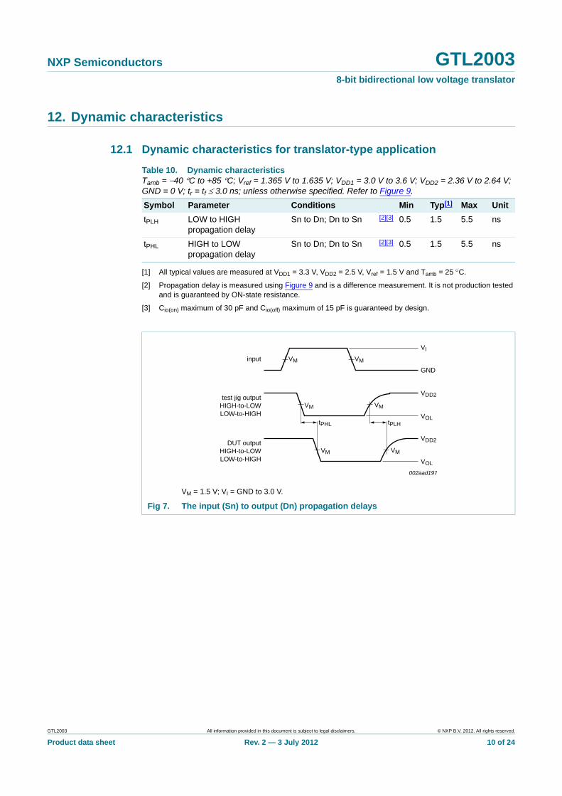
12. Dynamic characteristics
12.1 Dynamic characteristics for translator-type application
[1] All typical values are measured at VDD1 = 3.3 V, VDD2 = 2.5 V, Vref = 1.5 V and Tamb = 25 C.
[2] Propagation delay is measured using Figure 9 and is a difference measurement. It is not production tested and is guaranteed by ON-state resistance.
[3] Cio(on) maximum of 30 pF and Cio(off) maximum of 15 pF is guaranteed by design.
Table 10. Dynamic characteristicsTamb = 40 C to +85 C; Vref = 1.365 V to 1.635 V; VDD1 = 3.0 V to 3.6 V; VDD2 = 2.36 V to 2.64 V; GND = 0 V; tr = tf 3.0 ns; unless otherwise specified. Refer to Figure 9.
Symbol Parameter Conditions Min Typ[1] Max Unit
tPLH LOW to HIGH propagation delay
Sn to Dn; Dn to Sn [2][3] 0.5 1.5 5.5 ns
tPHL HIGH to LOW propagation delay
Sn to Dn; Dn to Sn [2][3] 0.5 1.5 5.5 ns
VM = 1.5 V; VI = GND to 3.0 V.
Fig 7. The input (Sn) to output (Dn) propagation delays
VI
GND
VDD2
VM VMinput
test jig outputHIGH-to-LOWLOW-to-HIGH
VM VM
VOL
VDD2DUT outputHIGH-to-LOWLOW-to-HIGH
VM VM
VOL
002aad197
tPHL tPLH
GTL2003 All information provided in this document is subject to legal disclaimers. © NXP B.V. 2012. All rights reserved.
Product data sheet Rev. 2 — 3 July 2012 10 of 24

NXP Semiconductors GTL20038-bit bidirectional low voltage translator
12.2 Dynamic characteristics for CBT-type application
[1] This parameter is warranted by the ON-state resistance, but is not production tested. The propagation delay is based on the RC time constant of the typical ON-state resistance of the switch and a load capacitance of 50 pF, when driven by an ideal voltage source (zero output impedance).
Table 11. Dynamic characteristicsTamb = 40 C to +85 C; VGREF = 5 V 0.5 V; GND = 0 V; CL = 50 pF; unless otherwise specified. Refer to Figure 10.
Symbol Parameter Conditions Min Typ Max Unit
tPD propagation delay [1] - - 250 ps
VM = 1.5 V; VI = GND to 3.0 V.
tPD is equal to the maximum of tPLH or tPHL.
Fig 8. Input (Sn) to output (Dn) propagation delays
002aab664
3.0 V
0 V
VOH
VOL
tPLH tPHL
1.5 V 1.5 Vinput
output 1.5 V1.5 V
GTL2003 All information provided in this document is subject to legal disclaimers. © NXP B.V. 2012. All rights reserved.
Product data sheet Rev. 2 — 3 July 2012 11 of 24
NXP Semiconductors GTL20038-bit bidirectional low voltage translator
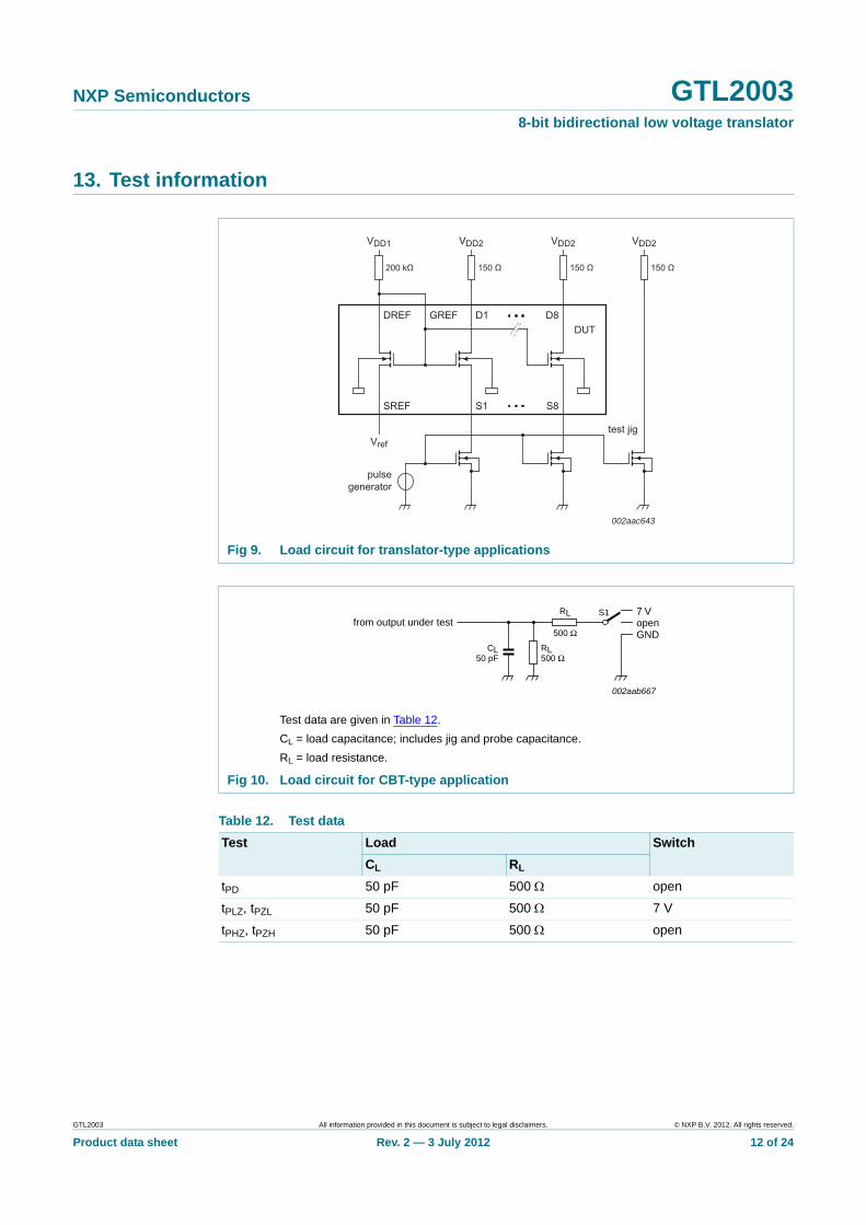
13. Test information
Fig 9. Load circuit for translator-type applications
Test data are given in Table 12.
CL = load capacitance; includes jig and probe capacitance.
RL = load resistance.
Fig 10. Load circuit for CBT-type application
Table 12. Test data
Test Load Switch
CL RL
tPD 50 pF 500 open
tPLZ, tPZL 50 pF 500 7 V
tPHZ, tPZH 50 pF 500 open
GREF
SREF
DREF
S1
D1
002aac643
S8
D8DUT
VDD1 VDD2 VDD2
200 kΩ 150 Ω 150 Ω
VDD2
150 Ω
Vref
pulsegenerator
test jig
CL50 pF
002aab667
RL500 Ω
from output under test7 VopenGND
S1RL
500 Ω
GTL2003 All information provided in this document is subject to legal disclaimers. © NXP B.V. 2012. All rights reserved.
Product data sheet Rev. 2 — 3 July 2012 12 of 24

NXP Semiconductors GTL20038-bit bidirectional low voltage translator
14. Package outline
Fig 11. Package outline SOT360-1 (TSSOP20)
UNIT A1 A2 A3 bp c D (1) E (2) (1)e HE L Lp Q Zywv θ
REFERENCESOUTLINEVERSION
EUROPEANPROJECTION ISSUE DATE
IEC JEDEC JEITA
mm 0.150.05
0.950.80
0.300.19
0.20.1
6.66.4
4.54.3
0.656.66.2
0.40.3
0.50.2
80
o
o0.13 0.10.21
DIMENSIONS (mm are the original dimensions)
Notes
1. Plastic or metal protrusions of 0.15 mm maximum per side are not included.
2. Plastic interlead protrusions of 0.25 mm maximum per side are not included.
0.750.50
SOT360-1 MO-15399-12-2703-02-19
w Mbp
D
Z
e
0.25
1 10
20 11
pin 1 index
θ
AA1
A2
Lp
Q
detail X
L
(A )3
HE
E
c
v M A
XA
y
0 2.5 5 mm
scale
TSSOP20: plastic thin shrink small outline package; 20 leads; body width 4.4 mm SOT360-1
Amax.
1.1
GTL2003 All information provided in this document is subject to legal disclaimers. © NXP B.V. 2012. All rights reserved.
Product data sheet Rev. 2 — 3 July 2012 13 of 24

NXP Semiconductors GTL20038-bit bidirectional low voltage translator
Fig 12. Package outline SOT764-1 (DHVQFN20)
terminal 1index area
0.51
A1 EhbUNIT ye
0.2
c
REFERENCESOUTLINEVERSION
EUROPEANPROJECTION ISSUE DATE
IEC JEDEC JEITA
mm 4.64.4
Dh
3.152.85
y1
2.62.4
1.150.85
e1
3.50.300.18
0.050.00
0.05 0.1
DIMENSIONS (mm are the original dimensions)
SOT764-1 MO-241 - - -- - -
0.50.3
L
0.1
v
0.05
w
0 2.5 5 mm
scale
SOT764-1DHVQFN20: plastic dual in-line compatible thermal enhanced very thin quad flat package; no leads;20 terminals; body 2.5 x 4.5 x 0.85 mm
A(1)
max.
AA1
c
detail X
yy1 Ce
L
Eh
Dh
e
e1
b
2 9
19 12
11
101
20
X
D
E
C
B A
terminal 1index area
ACC
Bv M
w M
E(1)
Note
1. Plastic or metal protrusions of 0.075 mm maximum per side are not included.
D(1)
02-10-1703-01-27
GTL2003 All information provided in this document is subject to legal disclaimers. © NXP B.V. 2012. All rights reserved.
Product data sheet Rev. 2 — 3 July 2012 14 of 24

NXP Semiconductors GTL20038-bit bidirectional low voltage translator
15. Soldering of SMD packages
This text provides a very brief insight into a complex technology. A more in-depth account of soldering ICs can be found in Application Note AN10365 “Surface mount reflow soldering description”.
15.1 Introduction to soldering
Soldering is one of the most common methods through which packages are attached to Printed Circuit Boards (PCBs), to form electrical circuits. The soldered joint provides both the mechanical and the electrical connection. There is no single soldering method that is ideal for all IC packages. Wave soldering is often preferred when through-hole and Surface Mount Devices (SMDs) are mixed on one printed wiring board; however, it is not suitable for fine pitch SMDs. Reflow soldering is ideal for the small pitches and high densities that come with increased miniaturization.
15.2 Wave and reflow soldering
Wave soldering is a joining technology in which the joints are made by solder coming from a standing wave of liquid solder. The wave soldering process is suitable for the following:
• Through-hole components
• Leaded or leadless SMDs, which are glued to the surface of the printed circuit board
Not all SMDs can be wave soldered. Packages with solder balls, and some leadless packages which have solder lands underneath the body, cannot be wave soldered. Also, leaded SMDs with leads having a pitch smaller than ~0.6 mm cannot be wave soldered, due to an increased probability of bridging.
The reflow soldering process involves applying solder paste to a board, followed by component placement and exposure to a temperature profile. Leaded packages, packages with solder balls, and leadless packages are all reflow solderable.
Key characteristics in both wave and reflow soldering are:
• Board specifications, including the board finish, solder masks and vias
• Package footprints, including solder thieves and orientation
• The moisture sensitivity level of the packages
• Package placement
• Inspection and repair
• Lead-free soldering versus SnPb soldering
15.3 Wave soldering
Key characteristics in wave soldering are:
• Process issues, such as application of adhesive and flux, clinching of leads, board transport, the solder wave parameters, and the time during which components are exposed to the wave
• Solder bath specifications, including temperature and impurities
GTL2003 All information provided in this document is subject to legal disclaimers. © NXP B.V. 2012. All rights reserved.
Product data sheet Rev. 2 — 3 July 2012 15 of 24
NXP Semiconductors GTL20038-bit bidirectional low voltage translator
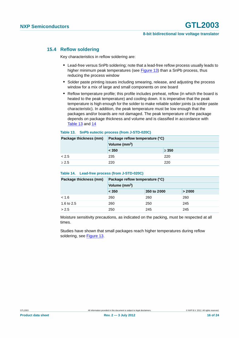
15.4 Reflow soldering
Key characteristics in reflow soldering are:
• Lead-free versus SnPb soldering; note that a lead-free reflow process usually leads to higher minimum peak temperatures (see Figure 13) than a SnPb process, thus reducing the process window
• Solder paste printing issues including smearing, release, and adjusting the process window for a mix of large and small components on one board
• Reflow temperature profile; this profile includes preheat, reflow (in which the board is heated to the peak temperature) and cooling down. It is imperative that the peak temperature is high enough for the solder to make reliable solder joints (a solder paste characteristic). In addition, the peak temperature must be low enough that the packages and/or boards are not damaged. The peak temperature of the package depends on package thickness and volume and is classified in accordance with Table 13 and 14
Moisture sensitivity precautions, as indicated on the packing, must be respected at all times.
Studies have shown that small packages reach higher temperatures during reflow soldering, see Figure 13.
Table 13. SnPb eutectic process (from J-STD-020C)
Package thickness (mm) Package reflow temperature (C)
Volume (mm3)
< 350 350
< 2.5 235 220
2.5 220 220
Table 14. Lead-free process (from J-STD-020C)
Package thickness (mm) Package reflow temperature (C)
Volume (mm3)
< 350 350 to 2000 > 2000
< 1.6 260 260 260
1.6 to 2.5 260 250 245
> 2.5 250 245 245
GTL2003 All information provided in this document is subject to legal disclaimers. © NXP B.V. 2012. All rights reserved.
Product data sheet Rev. 2 — 3 July 2012 16 of 24

NXP Semiconductors GTL20038-bit bidirectional low voltage translator
For further information on temperature profiles, refer to Application Note AN10365 “Surface mount reflow soldering description”.
MSL: Moisture Sensitivity Level
Fig 13. Temperature profiles for large and small components
001aac844
temperature
time
minimum peak temperature= minimum soldering temperature
maximum peak temperature= MSL limit, damage level
peak temperature
GTL2003 All information provided in this document is subject to legal disclaimers. © NXP B.V. 2012. All rights reserved.
Product data sheet Rev. 2 — 3 July 2012 17 of 24
NXP Semiconductors GTL20038-bit bidirectional low voltage translator
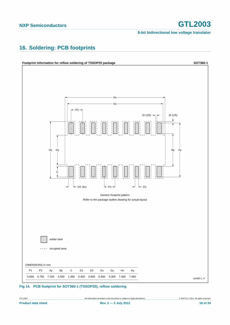
16. Soldering: PCB footprints
Fig 14. PCB footprint for SOT360-1 (TSSOP20); reflow soldering
DIMENSIONS in mm
Ay By D1 D2 Gy HyP1 C Gx
sot360-1_fr
Hx
SOT360-1
solder land
occupied area
Footprint information for reflow soldering of TSSOP20 package
AyByGy
C
Hy
Hx
Gx
P1
Generic footprint pattern
Refer to the package outline drawing for actual layout
P2
(0.125) (0.125)
D1D2 (4x)
P2
7.200 4.500 1.350 0.400 0.600 6.900 5.300 7.4507.3000.650 0.750
GTL2003 All information provided in this document is subject to legal disclaimers. © NXP B.V. 2012. All rights reserved.
Product data sheet Rev. 2 — 3 July 2012 18 of 24
NXP Semiconductors GTL20038-bit bidirectional low voltage translator
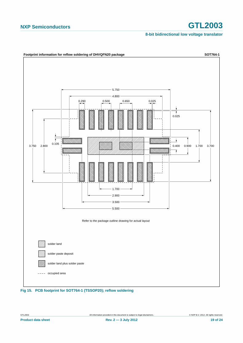
Fig 15. PCB footprint for SOT764-1 (TSSOP20); reflow soldering
SOT764-1Footprint information for reflow soldering of DHVQFN20 package
Refer to the package outline drawing for actual layout
occupied area
solder land plus solder paste
solder land
solder paste deposit
0.400
0.650 0.025
4.800
5.750
0.5000.290
1.700
2.900
3.500
5.500
0.900 1.700 3.7003.750 2.8000.105
0.025
GTL2003 All information provided in this document is subject to legal disclaimers. © NXP B.V. 2012. All rights reserved.
Product data sheet Rev. 2 — 3 July 2012 19 of 24

NXP Semiconductors GTL20038-bit bidirectional low voltage translator
17. Abbreviations
18. References
[1] AN11127, “Bidirectional voltage translators NVT2001/02/03/04/06/08/10, PCA9306, GTL2000/02/03/10” — application note; NXP Semiconductors; www.nxp.com/documents/application_note/AN11127.pdf
[2] AN10145, “Bidirectional low voltage translators” — application note; NXP Semiconductors; www.nxp.com/documents/application_note/AN10145.pdf
Table 15. Abbreviations
Acronym Description
CDM Charged Device Model
CMOS Complementary Metal Oxide Semiconductor
DUT Device Under Test
ESD ElectroStatic Discharge
GTL Gunning Transceiver Logic
HBM Human Body Model
I2C-bus Inter-Integrated Circuit bus
LVTTL Low Voltage Transistor-Transistor Logic
NMOS Negative-channel Metal Oxide Semiconductor
TTL Transistor-Transistor Logic
TVC Transceiver Voltage Clamps
GTL2003 All information provided in this document is subject to legal disclaimers. © NXP B.V. 2012. All rights reserved.
Product data sheet Rev. 2 — 3 July 2012 20 of 24

NXP Semiconductors GTL20038-bit bidirectional low voltage translator
19. Revision history
Table 16. Revision history
Document ID Release date Data sheet status Change notice Supersedes
GTL2003 v.2 20120703 Product data sheet - GTL2003 v.1
Modifications: • Section 1 “General description”:
– first paragraph, third sentence changed from “between 1.0 V and 5.0 V” to “between 0.8 V and 5.0 V”
– first paragraph: added (new) fourth sentence.
– second paragraph, third sentence: changed from “VCC” to “VDD1”
• Section 2 “Features and benefits”:
– second bullet: added “0.8 V, 0.9 V”
– tenth bullet: deleted phrase “200 V MM per JESD22-A115”
• Section 3 “Applications”:
– first bullet: changed from “1.0 V” to “0.8 V” (two places)
– second bullet: added “0.8 V, 0.9 V”
• Table 5 “Function selection, LOW-to-HIGH translation”, Table note [3]: changed from “VCC” to “VDD1”
• Section 8.1 “Bidirectional translation”:
– first sentence: changed from “VCC” to “VDD1”
– third sentence: changed from “VCC” to “VDD1”
– seventh sentence re-written
– eighth sentence re-written
– added (new) ninth sentence
– Figure 4 “Bidirectional translation to multiple higher voltage levels such as an I2C-bus application” updated
• Section 8.2 “Unidirectional down translation”:
– first sentence: changed from “VCC” to “VDD1”
– fifth sentence re-written (split into fifth and sixth sentences)
– added (new) seventh sentence
– Figure 5 “Unidirectional down translation to protect low voltage processor pins” updated
• Figure 6 “Unidirectional down translation to protect low voltage processor pins” updated
• Section 8.4 “Sizing pull-up resistor”:
– added (new) second paragraph
– third paragraph, first sentence: appended “for VDD1 VSREF 1.5 V”
– Table 6 “Pull-up resistor values”: added six rows, 1.1 V through 0.8 V
• Table 8 “Recommended operating conditions”: added row VSn
• Table 9 “Static characteristics”:
– Conditions for Ron: changed from “VI” to “VSn”
• Figure 9 “Load circuit for translator-type applications”: corrected resistors’ values from “150 k” to “150 ” (3 places)
• Added Section 16 “Soldering: PCB footprints”
• Added Section 18 “References”
GTL2003_1 20070727 Product data sheet - -
GTL2003 All information provided in this document is subject to legal disclaimers. © NXP B.V. 2012. All rights reserved.
Product data sheet Rev. 2 — 3 July 2012 21 of 24

NXP Semiconductors GTL20038-bit bidirectional low voltage translator
20. Legal information
20.1 Data sheet status
[1] Please consult the most recently issued document before initiating or completing a design.
[2] The term ‘short data sheet’ is explained in section “Definitions”.
[3] The product status of device(s) described in this document may have changed since this document was published and may differ in case of multiple devices. The latest product status information is available on the Internet at URL http://www.nxp.com.
20.2 Definitions
Draft — The document is a draft version only. The content is still under internal review and subject to formal approval, which may result in modifications or additions. NXP Semiconductors does not give any representations or warranties as to the accuracy or completeness of information included herein and shall have no liability for the consequences of use of such information.
Short data sheet — A short data sheet is an extract from a full data sheet with the same product type number(s) and title. A short data sheet is intended for quick reference only and should not be relied upon to contain detailed and full information. For detailed and full information see the relevant full data sheet, which is available on request via the local NXP Semiconductors sales office. In case of any inconsistency or conflict with the short data sheet, the full data sheet shall prevail.
Product specification — The information and data provided in a Product data sheet shall define the specification of the product as agreed between NXP Semiconductors and its customer, unless NXP Semiconductors and customer have explicitly agreed otherwise in writing. In no event however, shall an agreement be valid in which the NXP Semiconductors product is deemed to offer functions and qualities beyond those described in the Product data sheet.
20.3 Disclaimers
Limited warranty and liability — Information in this document is believed to be accurate and reliable. However, NXP Semiconductors does not give any representations or warranties, expressed or implied, as to the accuracy or completeness of such information and shall have no liability for the consequences of use of such information. NXP Semiconductors takes no responsibility for the content in this document if provided by an information source outside of NXP Semiconductors.
In no event shall NXP Semiconductors be liable for any indirect, incidental, punitive, special or consequential damages (including - without limitation - lost profits, lost savings, business interruption, costs related to the removal or replacement of any products or rework charges) whether or not such damages are based on tort (including negligence), warranty, breach of contract or any other legal theory.
Notwithstanding any damages that customer might incur for any reason whatsoever, NXP Semiconductors’ aggregate and cumulative liability towards customer for the products described herein shall be limited in accordance with the Terms and conditions of commercial sale of NXP Semiconductors.
Right to make changes — NXP Semiconductors reserves the right to make changes to information published in this document, including without limitation specifications and product descriptions, at any time and without notice. This document supersedes and replaces all information supplied prior to the publication hereof.
Suitability for use — NXP Semiconductors products are not designed, authorized or warranted to be suitable for use in life support, life-critical or safety-critical systems or equipment, nor in applications where failure or malfunction of an NXP Semiconductors product can reasonably be expected to result in personal injury, death or severe property or environmental damage. NXP Semiconductors and its suppliers accept no liability for inclusion and/or use of NXP Semiconductors products in such equipment or applications and therefore such inclusion and/or use is at the customer’s own risk.
Applications — Applications that are described herein for any of these products are for illustrative purposes only. NXP Semiconductors makes no representation or warranty that such applications will be suitable for the specified use without further testing or modification.
Customers are responsible for the design and operation of their applications and products using NXP Semiconductors products, and NXP Semiconductors accepts no liability for any assistance with applications or customer product design. It is customer’s sole responsibility to determine whether the NXP Semiconductors product is suitable and fit for the customer’s applications and products planned, as well as for the planned application and use of customer’s third party customer(s). Customers should provide appropriate design and operating safeguards to minimize the risks associated with their applications and products.
NXP Semiconductors does not accept any liability related to any default, damage, costs or problem which is based on any weakness or default in the customer’s applications or products, or the application or use by customer’s third party customer(s). Customer is responsible for doing all necessary testing for the customer’s applications and products using NXP Semiconductors products in order to avoid a default of the applications and the products or of the application or use by customer’s third party customer(s). NXP does not accept any liability in this respect.
Limiting values — Stress above one or more limiting values (as defined in the Absolute Maximum Ratings System of IEC 60134) will cause permanent damage to the device. Limiting values are stress ratings only and (proper) operation of the device at these or any other conditions above those given in the Recommended operating conditions section (if present) or the Characteristics sections of this document is not warranted. Constant or repeated exposure to limiting values will permanently and irreversibly affect the quality and reliability of the device.
Terms and conditions of commercial sale — NXP Semiconductors products are sold subject to the general terms and conditions of commercial sale, as published at http://www.nxp.com/profile/terms, unless otherwise agreed in a valid written individual agreement. In case an individual agreement is concluded only the terms and conditions of the respective agreement shall apply. NXP Semiconductors hereby expressly objects to applying the customer’s general terms and conditions with regard to the purchase of NXP Semiconductors products by customer.
No offer to sell or license — Nothing in this document may be interpreted or construed as an offer to sell products that is open for acceptance or the grant, conveyance or implication of any license under any copyrights, patents or other industrial or intellectual property rights.
Document status[1][2] Product status[3] Definition
Objective [short] data sheet Development This document contains data from the objective specification for product development.
Preliminary [short] data sheet Qualification This document contains data from the preliminary specification.
Product [short] data sheet Production This document contains the product specification.
GTL2003 All information provided in this document is subject to legal disclaimers. © NXP B.V. 2012. All rights reserved.
Product data sheet Rev. 2 — 3 July 2012 22 of 24
NXP Semiconductors GTL20038-bit bidirectional low voltage translator
Export control — This document as well as the item(s) described herein may be subject to export control regulations. Export might require a prior authorization from competent authorities.
Non-automotive qualified products — Unless this data sheet expressly states that this specific NXP Semiconductors product is automotive qualified, the product is not suitable for automotive use. It is neither qualified nor tested in accordance with automotive testing or application requirements. NXP Semiconductors accepts no liability for inclusion and/or use of non-automotive qualified products in automotive equipment or applications.
In the event that customer uses the product for design-in and use in automotive applications to automotive specifications and standards, customer (a) shall use the product without NXP Semiconductors’ warranty of the product for such automotive applications, use and specifications, and (b) whenever customer uses the product for automotive applications beyond
NXP Semiconductors’ specifications such use shall be solely at customer’s own risk, and (c) customer fully indemnifies NXP Semiconductors for any liability, damages or failed product claims resulting from customer design and use of the product for automotive applications beyond NXP Semiconductors’ standard warranty and NXP Semiconductors’ product specifications.
Translations — A non-English (translated) version of a document is for reference only. The English version shall prevail in case of any discrepancy between the translated and English versions.
20.4 TrademarksNotice: All referenced brands, product names, service names and trademarks are the property of their respective owners.
21. Contact information
For more information, please visit: http://www.nxp.com
For sales office addresses, please send an email to: [email protected]
GTL2003 All information provided in this document is subject to legal disclaimers. © NXP B.V. 2012. All rights reserved.
Product data sheet Rev. 2 — 3 July 2012 23 of 24

NXP Semiconductors GTL20038-bit bidirectional low voltage translator
22. Contents
1 General description . . . . . . . . . . . . . . . . . . . . . . 1
2 Features and benefits . . . . . . . . . . . . . . . . . . . . 1
3 Applications . . . . . . . . . . . . . . . . . . . . . . . . . . . . 2
4 Ordering information. . . . . . . . . . . . . . . . . . . . . 24.1 Ordering options . . . . . . . . . . . . . . . . . . . . . . . . 2
5 Functional diagram . . . . . . . . . . . . . . . . . . . . . . 2
6 Pinning information. . . . . . . . . . . . . . . . . . . . . . 36.1 Pinning . . . . . . . . . . . . . . . . . . . . . . . . . . . . . . . 36.2 Pin description . . . . . . . . . . . . . . . . . . . . . . . . . 3
7 Functional description . . . . . . . . . . . . . . . . . . . 47.1 Function selection. . . . . . . . . . . . . . . . . . . . . . . 4
8 Application design-in information . . . . . . . . . . 58.1 Bidirectional translation . . . . . . . . . . . . . . . . . . 58.2 Unidirectional down translation. . . . . . . . . . . . . 68.3 Unidirectional up translation . . . . . . . . . . . . . . . 68.4 Sizing pull-up resistor . . . . . . . . . . . . . . . . . . . . 7
9 Limiting values. . . . . . . . . . . . . . . . . . . . . . . . . . 8
10 Recommended operating conditions. . . . . . . . 8
11 Static characteristics. . . . . . . . . . . . . . . . . . . . . 9
12 Dynamic characteristics . . . . . . . . . . . . . . . . . 1012.1 Dynamic characteristics for translator-type
application . . . . . . . . . . . . . . . . . . . . . . . . . . . 1012.2 Dynamic characteristics for CBT-type
application . . . . . . . . . . . . . . . . . . . . . . . . . . . 11
13 Test information. . . . . . . . . . . . . . . . . . . . . . . . 12
14 Package outline . . . . . . . . . . . . . . . . . . . . . . . . 13
15 Soldering of SMD packages . . . . . . . . . . . . . . 1515.1 Introduction to soldering . . . . . . . . . . . . . . . . . 1515.2 Wave and reflow soldering . . . . . . . . . . . . . . . 1515.3 Wave soldering . . . . . . . . . . . . . . . . . . . . . . . . 1515.4 Reflow soldering . . . . . . . . . . . . . . . . . . . . . . . 16
16 Soldering: PCB footprints. . . . . . . . . . . . . . . . 18
17 Abbreviations. . . . . . . . . . . . . . . . . . . . . . . . . . 20
18 References . . . . . . . . . . . . . . . . . . . . . . . . . . . . 20
19 Revision history. . . . . . . . . . . . . . . . . . . . . . . . 21
20 Legal information. . . . . . . . . . . . . . . . . . . . . . . 2220.1 Data sheet status . . . . . . . . . . . . . . . . . . . . . . 2220.2 Definitions. . . . . . . . . . . . . . . . . . . . . . . . . . . . 2220.3 Disclaimers . . . . . . . . . . . . . . . . . . . . . . . . . . . 2220.4 Trademarks. . . . . . . . . . . . . . . . . . . . . . . . . . . 23
21 Contact information. . . . . . . . . . . . . . . . . . . . . 23
22 Contents . . . . . . . . . . . . . . . . . . . . . . . . . . . . . . 24
© NXP B.V. 2012. All rights reserved.
For more information, please visit: http://www.nxp.comFor sales office addresses, please send an email to: [email protected]
Date of release: 3 July 2012
Document identifier: GTL2003
Please be aware that important notices concerning this document and the product(s)described herein, have been included in section ‘Legal information’.