gti 5g device rf component research report...gti 5g device rf component research report 4...
TRANSCRIPT

GTI 5G Device RF Component Research Report
1
GTI 5G Device
RF Component
Research Report
http://www.gtigroup.org

GTI 5G Device RF Component Research Report
2
GTI 5G Device RF Component
Research Report
Version: V1.0
Deliverable Type Procedural Document
√ Working Document
Confidential Level √ Open to GTI Operator Members
√ Open to GTI Partners
Open to Public
Working Group Terminal WG
Task
Source members
Support members
Editor China Mobile, Qorvo, HiWafer, Soitec, Skyworks, TAIYO
YUDEN, Murata, VanChip
Last Edit Date Feb. 2nd , 2018
Approval Date Feb. 9th , 2018

GTI 5G Device RF Component Research Report
3

GTI 5G Device RF Component Research Report
4
Confidentiality: This document may contain information that is confidential and access to
this document is restricted to the persons listed in the Confidential Level. This document
may not be used, disclosed or reproduced, in whole or in part, without the prior written
authorization of GTI, and those so authorized may only use this document for the purpose
consistent with the authorization. GTI disclaims any liability for the accuracy or completeness
or timeliness of the information contained in this document. The information contained in
this document may be subject to change without prior notice.
Document History
Date Meeting # Version # Revision Contents
02-02-2018 #21 v1.0 GTI 5G Device RF Component Research Report
DD-MM-YYY
Y
DD-MM-YYY
Y
DD-MM-YYY
Y
DD-MM-YYY
Y

GTI 5G Device RF Component Research Report
5
Table of Contents
1 Executive Summary............................................................................................................ 7
2 Abbreviations ..................................................................................................................... 8
3 Introduction ..................................................................................................................... 10
4 References ....................................................................................................................... 12
5 5G Device RF Component Industry Status ....................................................................... 15
6 Sub-6GHz 5G Device RF Component ............................................................................... 18
6.1 Sub-6GHz 5G Power Amplifier ............................................................................... 18
6.1.1 Existing Mobile Device Commercial Power Amplifier ................................. 19
6.1.2 Sub-6GHz 5G Power Amplifier Design ......................................................... 22
6.2 Sub-6GHz 5G Filter ................................................................................................ 33
6.2.1 Existing Mobile Device Commercial Filter ................................................... 33
6.2.2 3.3GHz-4.2GHz 5G Filter Design .................................................................. 41
6.2.3 4.4GHz-5GHz 5G Filter Design ..................................................................... 45
6.3 Sub-6GHz 5G Low Noise Amplifier ........................................................................ 46
6.3.1 Existing Mobile Device Commercial Low Noise Amplifier Products ............ 46
6.3.2 Sub-6GHz 5G Low Noise Amplifier Design .................................................. 47
7 mmWave 5G Device RF Component ................................................................................ 49
7.1 mmWave 5G Power Amplifier ............................................................................... 49
7.2 mmWave 5G Filter ................................................................................................. 51
7.3 mmWave 5G Low Noise Amplifier ......................................................................... 53
7.4 Switches for mmWave ........................................................................................... 54
7.4.1 What makes a ‘Great’ 5G Switch? ............................................................... 54
7.4.2 SOI Technology for 5G Switching ................................................................. 55
8 Related ‘Black Technologies’ ............................................................................................ 55
8.1 Engineered Substrate ............................................................................................ 55
8.1.1 What is 'Engineered Substrate'? ................................................................. 55

GTI 5G Device RF Component Research Report
6
8.1.2 Why do we need 'Engineered Substrate'? .................................................. 57
8.1.3 Application .................................................................................................. 60
8.2 Engineered Substrate: 'Anything on Anything' ...................................................... 61
8.2.1 Smart Cut™ .................................................................................................. 62
8.2.2 Smart Stacking™ .......................................................................................... 64
8.2.3 Epitaxy ......................................................................................................... 65
8.3 CMOS on SOL ......................................................................................................... 66
8.3.1 CMOS on SOI basics ..................................................................................... 67
8.3.2 Basic SOI Advantages .................................................................................. 68
8.3.3 PD-SOI and FD-SOI – Definition ................................................................... 69
8.3.4 Floating body and Body contact .................................................................. 70
8.4 CMOS on SOI for RF ............................................................................................... 71
8.4.1 RF-SOI .......................................................................................................... 71
8.4.2 PD-SOI for RF ............................................................................................... 81
8.4.3 FD-SOI .......................................................................................................... 83
8.5 Non Silicon Engineered Substrate ......................................................................... 93
8.5.1 Non Silicon materials for RF ........................................................................ 93
8.5.2 Example 1: Indium Phosphide on Gallium Arsenide ................................... 96
8.5.3 Example 2: Piezo on Insulator ..................................................................... 97

GTI 5G Device RF Component Research Report
7
1 Executive Summary
How to realize “high efficiency and low power consumption” device is a technical issue which
should be emphasized on throughout the 5G RF component R&D process. The power
consumption should be optimized based on the deployment plan of operators and the
requirements of customers. This process should involve not only RF component vendors, but
also chipset vendors and device vendors.
RF FEM is one of the most popular solutions to realize 5G NR RF components, especially for
the large volume of high-end devices, due to its smaller layout area, better inter-stage
matching, less design inputs, shorter test process and faster time to market. So FEM is a
research and development direction worthy of attention.
According to 3GPP’s schedule, the first version of 5G standard R15 will be completed in the
middle of 2018 and R16 is going to be completed by the end of 2019. The 5G+ technical
specification will be constantly updated since 2020. It is hoped that RF components vendors
could actively participate in and track 3GPP’s discussion on the specifications of 5G RF
components as well as establish theoretical basis for the final specifications based on the
prospective simulation and test data. In order to guarantee commercial RF components in
time, RF components designers and manufactures should work together with operators,
chipset vendors, device vendors and test instrument vendors to make sure the system
verification and the pre-commercial trial could be completed in 2018 and 2019 separately
The high performance and low cost front-end RF components are expected to be provided in
proper time and volume. So the RF component vendors are supposed to cooperate with the
whole industrial chain to accomplish the goal of 5G’s commercialization by the end of 2020.
GTI 5G Device Component Research Report is expected to help people to develop 5G devices
and to promote industrial development. This report may also help people to know more
about the industrial status of 5G device RF components. Meanwhile, it may also help readers
interested in 5G device RF components to gain from the further thinking.

GTI 5G Device RF Component Research Report
8
2 Abbreviations
Abbreviation Explanation
BAW bulk acoustic wave
CC Component Carrier
CMOS Complementary Metal Oxide Semiconductor
DC Dual Connectivity
eMBB Enhanced Mobile Broadband
ESD Electro-Static discharge
FBB Forward Back Gate bias
FBAR Film Bulk Acoustic Resonator
FD Fully Depleted
gNB NR node
HEMT High Electron Mobility Transistor
HSP Harmonic Suppression Process
HPUE High Power UE
IPD Integrated Product Development
LTCC Low Temperature Co-fired Ceramic
MEMS Micro-Electro-Mechanical System
MIMO Multiple-Input Multiple-Output
mMTC Massive Machine Type Communication
mmWave Millimeter Wave
MMMB Multimode Multiband
MMIC Monolithic Microwave Integrated Circuit
MOSFET Metal–Oxide–Semiconductor Field-Effect Transistor
MU-MIMO Multi-User MIMO
NSA Non-Standalone
OFDM Orthogonal Frequency Division Multiplexing
pHEMT Pseudomorphic HEMT
PPAC Performance, Power, Area, and Cost
PAE Power Added Efficiency
PD Partially Depleted
RFeSI RF enhanced Signal Integrity
RFFE Radio Frequency Front-end

GTI 5G Device RF Component Research Report
9
SAW surface acoustic wave
SA Standalone
SOI Silicon on Insulator
SIMOX Separation by Implantation of Oxygen
SU-MIMO Single-User MIMO
UE User Equipment
URLLC Ultra-Reliable and Low Latency Communications
UTBB Ultra Thin Body and Box
3GPP The 3rd Generation Partnership Project

GTI 5G Device RF Component Research Report
10
3 Introduction
4G has completely changed our lives. While, as the society becomes much more informative,
people’s requirements increase rapidly. Devices are supposed to have better performance
and provide more qualified service. Thus more and more opportunities and changes are
created for mobile communication. Compared with 4G, 5G would have higher experiencing
speed, higher connection density and lower latency. Not only the connections between
people and people, but also people and things, things and things would be included into 5G
scope. Aiming at constructing a cross industry ecosystem and further changing people’s lives,
5G sets its sights on enhanced Mobile Broad Band (eMBB), massive Machine Type
Communication (mMTC) as well as Ultra Reliable and Low Latency Communication.
China Mobile plays an important role in prompting 5G to enter the commercial stage before
2020. As the leader of the IMT-2020 requirement group, China Mobile led to complete ‘5G
Vision and Requirement’ White Paper as well as the 5G requirements in NGMN and the 5G
requirements and scenarios in 3GPP. Aiming for 5G’s commercialization in 2020, sub-6GHz is
the focus at this moment. Considering the millimeter Wave spectrum won’t be used for
mobile telecommunication until 2019 and after that 2~3 years will be needed for spectrum
allocation in China, the commercialization of 5G mmWave might be 2022 or even later.
Before the commercialization in 2020, China Mobile will complete the 3-phase validation of
5G, the key technology test, the system test and the large-scale test. The key technology test
has been completed in 2016, and the system test has also been completed in 2017. The
large-scale test is expected to start in 2018. With the purpose of specifying the direction in
developing testing prototypes, China Mobile released ’Guideline for 3.5GHz 5G System
Prototype and Trial’ in the early 2017 and jointly released the ’GTI Sub-6GHz 5G Device
Whitepaper’ in Nov. 2017 with GTI industrial partners. The guideline and the white paper
analyzed the key technologies as well as the hot topics and difficult problems in the
implementation of 5G pre-commercial/commercial devices. Many problems are related to
5G device RF components. So the implementation of RF components has become the key
link to realize the 5G devices.
Therefore, co-operating with China Mobile 5G Innovation Center, GTI Device Working Group
leads to write this “GTI 5G Device RF Component Research Report” with the industrial
partners. This report mainly focuses on the 5G device RF components and has been carried
out in two directions respectively, the sub-6GHz RF components and the millimeter wave RF
components. Combined with the consideration of integrated circuit technology, the report
analyses the industrial status, key technologies, design challenges, alternative process and
research progress of core 5G RF components, such as power amplifier, filter, low noise
amplifier and switch. Some related ‘Black Technologies’ which may have great influence on
future RF components are also introduced in the report.
We sincerely thank all the contributors for their hard work in writing this report.

GTI 5G Device RF Component Research Report
11
Chapter 5 5G Device RF Component Industry Status: HiWafer, Soitec, Qorvo, Skyworks, TAIYO
YUDEN, Murata and VanChip, etc.
Chapter 6 Sub-6GHz 5G Device RF Component
6.1 Sub-6GHz 5G Power Amplifier: Skyworks, Qorvo, VanChip and HiWafer, etc.
6.2 Sub-6GHz 5G Filter: TAIYO YUDEN and Qorvo, ect.
6.3 Sub-6GHz 5G Low Noise Amplifier: Qorvo and HiWafer, etc.
Chapter 7 mmWave 5G Device RF Component: HiWafer, Murata and Qorvo, etc.
Chapter 8 Related ‘Black Technologies’: Soitec, Qorvo and Skyworks, etc.
Special thanks to the following contributors:
China Mobile 5G Innovation Center
China Mobile Research Institute
Dan Song, Yifan Liu, Shuai Ma, Shanpeng Xiao and Guang Yang.
Qorvo
Zhen Tao (Lawrence Tao)
Chengdu HiWafer Semiconductor Co., Ltd.
Yifeng Chen, Ting Peng, Chang Wu, Ting Fu, Xin Kong, Chunjiang Li, Yuan Zhai
Soitec
Bowen Lin (Stephen Lin), Eric Desbonnet and Manuel Sellier
Skyworks Solutions, Inc.
Yan Sun (Ryan Sun) and Kevin Walsh
TAIYO YUDEN CO., LTD.
Mike Tanahashi, Ryan Gu and Tao Ma
Murata Manufacturing Co., Ltd.
Gang Lv
VanChip Technologies
Gang Chen
This report will be continuously updated according to the research and development

GTI 5G Device RF Component Research Report
12
progress.
4 References
The following documents contain provisions which, through reference in this text, constitute
provisions of the present document.
[1] W-band low noise amplifier based on 70nm GaAs MHEMT process, Shaobing Wu, Weibo
Wang, Fangjin Guo, Jianfeng Gao and Nianning Huang, Research and progress of SSE, April
2017.
[2] Research on InP HBT device module and circus. Rui Liu, Xi'an Electronic and Engineering
University, 2014.
[3] Development and application of Inp HEMT and Inp HBT, Lihua Yao, Semiconductor
technology, November 2009.
[4] Design of X-band broadband low noise amplifier MMIC, Dezhi Zhang, Jiaxiu Zhu, Jin Xu,
Journal of Microwaves, October 2008.
[5] 60G high gain broadband monolithic integrated low noise amplifier, Yang Hou, Jian Zhang,
Lingyun Li and Xiaowei Sun, Journal of Semiconductors, July 2008
[6] A wide-band low noise amplifier at Ka band, Haoquan Hu and Xuehui Tong, Electronic
information warfare technology, July 2006.
[7] Ka-band monolithic low noise amplifier, Hao Yang, Hua Huang and Mingli Hao, Chinese
journal of electron devices, August 2007.
[8] Design of general pHEMT navigation low noise amplifier, Zhichen Tu, Zhejiang University,
2016.
[9] Research progress of w-band and above MMIC amplifiers, Hewei Li, Emiconductor
technology, July 2009.
[10] New developments of solid state microwave, millimeter-wave THz devices and circuits,

GTI 5G Device RF Component Research Report
13
Zhengping Zhao, Emiconductor technology, December 2011.
[11] Embrace a brand new cooperation in 5G era, China Mobile, Danni Song, SOI consortium
workshop Shanghai, September 2017
[12] RF circuit design using SOI, Leo Wilz, Skyworks, IMS 2017 short course
[13] High frequency and mm-wave Noise in SOI based CMOS: from Noise Principles to
Characterizations Techniques, IEMN, Gilles Dambrine, IMS 2017 short course
[14] Benefits of 45nm Advanced Node Process for RFSOI and Applicability of a Passive Inter
modulation Approach, Global Foundries, Thomas McKay, IMS 2017 short course
[15] Innovative Characterization Techniques of SOI for RF Applications, Incize, Mostafa Emam,
IMS 2017 short course
[16] RF SOI from material to devices, UCL, Prof. Jean-Pierre Raskin, IMS 2017 short course
[17] SOI, from basics to applications, UCL, Cecilia Gemino, David Bold, Denis Flandres, IMS
2017 short course
[18] Engineered SOI Substrates for RF Applications, Soitec, Frédéric Allibert, IMS 2017 short
course
[19] RFSOI-on-HR-Si Technologies for Wireless Reconfigurable Applications, Qorvo, Julio
Costa, SOI Consortium Shanghai 2015
[20] Silicon-on-Insulator (SOI) Switches for Cellular and WLAN Front-End Applications, RFMD,
Ali Tombak, IMS 2012
[21] Advanced SOI Technology for RF Applications, CEA-LETI, Christine Raynaud, SOI
conference short course, 2007
[22] An Introduction to SOI Applications : Low Power to Smart Power, Soitec, Mariam
Sadaka, S3S conference short course 2015
[23] 5G in Perspective - A Pragmatic Guide to What’s Next, Skyworks white paper, 2017The
SOI MOSFET, Tyndall National Institute, Dr Colinge, 2008
[24] Review of RF SOI Technology: a 10 years economic success story now looking toward
5G, STM, Frédéric Gianesello, S3S 2015 short course

GTI 5G Device RF Component Research Report
14
[25] SOI overview and Assessment for Analog and Mixed-signal, UCL, Denis Flandres, SOI
workshop, 2008
[26] RF SOI Device Technology Overview, UCL, Prof Raskin, S3S 2014
[27] Silicon-On-Insulator (SOI) Technology 1st Edition Manufacture and Applications, Soitec,
O. Kononchuk B.-Y. Nguyen, 2014
[28] Engineering substrates new technology to accelerate 5G high frequency, Soitec, Stephen
Lin, Eric Desbonnets, 5G High Frequency workshop China Mobile 2017
[29] Engineered silicon on insulator substrates and others structures to support
Communication road map up to 5G, Eric Desbonnets, IWPC workshop 2016
[30] https://www.soitec.com/en

GTI 5G Device RF Component Research Report
15
5 5G Device RF Component Industry Status
Based on the Navian predication, the total market size of RF front-end modules for mobile
communications devices will grow from $ 7.9 billion in 2013 to $ 21.2 billion in 2019 at a
CAGR of 15.4%.
Figure 5-1 Navian Predication on RF Front End Module Market
At present, the RF front-end chip market is mainly divided into two categories: a class of
acoustic technology-based filters to surface acoustic wave filter (SAW) and Bulk acoustic
wave (BAW) as the representative, one is the use of semiconductor technology
Manufactured circuit chip, with power amplifier (PA) and switch circuit (Switch) as the
representative.
The traditional SAW filter market has become saturated, with Muruta, TDK and Taiyo Yuden
accounting for more than 80% of the global market. Murata Manufacturing Co., Ltd.
(Kabushiki-gaisha Murata Seisakusho) is a famous Japanese manufacturer of passive
electronic components, such as capacitors and inductors, which is founded in 1940s. Ever
since the beginning of the era of communications, Murata started business in RF aspects as
well. After expanding the product lineup of filters, Murata achieved acquisition of Renesas
Electronics and Peregrine Semiconductor, which leads to an integration of the lineup of RFFE
products. Nowadays the product lineup of wireless communications department of Murata
has almost covered all of the RFFE products including SAW and Multi-layer filters, RF
switches, modules of either transceiver-end or receiver-end, power amplifiers, and RF
connectors, etc. TAIYO YUDEN, after acquired Fujitsu Media Devices Ltd. in Y2010, has
extended its technology portfolio by adding SAW and FBAR technologies in addition to LTCC
RF device technology. Now the company is providing various RF devices (Filter, Duplexer,
Diplexer, Low Pass Filter, etc.) for 2G/3G and 4G. While the company has already been
working on the development of the series of Sub-6GHz filters for 5G since very early stages,
it has also completed the initial technology validation to cover up to mmW ranges including
both 28GHz and 39GHz frequency ranges in the light of upcoming 5G requirement which is
being standardized within 3GPP group at this time. These three core technologies,
SAW/FBAR/LTCC RF technologies, are indispensable for the implementation of upcoming 5G
standard and the company will continue to enhance these technologies and develop new
products through integrating three technologies.The current BAW core technologies are

GTI 5G Device RF Component Research Report
16
mainly in the hands of Broadcom (Avago) and Qorvo, as shown in Figure 5-2. According to
HIS data, Broadcom (Avago) and Qorvo have almost split their market share.
Figure 5-2 HIS Statistics on BAW Market Share (Up to 2014)
As shown in Figure 5-3, based on Navian's 2016 statistics, the device power amplifier market
has an estimated $ 13 billion market, forming the oligarchical competition between Skyworks,
Qorvo and Broadcom (Avago), which together accounted for 90% % of the market share.
Founded in 1962, Skyworks is an industry-leading RF front-end semiconductor solution
provider that designs and manufactures radio frequency (RF) for mobile handsets, cellular
network equipment, automotive, energy management, industrial and medical applications
And complete semiconductor system solutions, products include amplifiers, filters, switches,
attenuators, diodes, directional couplers, front-end modules. Qorvo is the new merger of RF
Micro Devices and TriQuint Semiconductor, two of the industry's leading RF solutions
companies. The combined Qorvo has two key product lines: the Mobile Device Product Line,
the Base Station and the Military Device Product Line, both of which Line for different
markets, but also in complementary areas of advanced technology research and
development. Broadcom, a maker of acquisition chips for Avago Technologies, has been
renamed Broadcom Limited to focus on III-V compound semiconductor design and process
technology, providing a broad range of analog, mixed-signal and optoelectronic components
product and system design and development. At present, major product lines include
Wireless communications, cable infrastructure, enterprise storage, industrial and others.

GTI 5G Device RF Component Research Report
17
Figure 5-3 Navian Statistics for the Device Power Amplifier Market (2016)
RF-device market is almost dominated by the International RF-device companies. As the
developments of 4G and 5G communication networks, the domestic RF-device companies
get more opportunities. Vanchip, a company running the IC design, measurement and sale
business, has lots of products used in 2G/3G communications. Lansus developed domestic
PA and RF switch in 2010. Its NZ5081 PA has been used in Yulong Coopad 8180 TD-SCDMA,
which is the first PA used in domestic smart phone. The customer of Lansus includes Mi,
Coolpad, ZTE and MEIZU. Hunstersun, a domestic 2G/3G/4G RF front end IC supplier, 600
millions sales in 2015. Products involved 3-mode-8-frequency, 5-mode-17-frequency, 2G
CMOS and 3G CMOS TxM RF front end ICs. So, the domestic RF IC companies have strong
ability of product developing.
RFIC manufacturing industry is accelerating while the RFIC design houses are blooming. In
the sub-6GHz band of 5G, HiWafer has developed 2um GaAs HBT process. As the mainstream
technology, this process realized the monolithic integrations of the active and passive
devices, which can provide better linearity, stability and reliability, This process also fits for
the 3G/4G cellphone, Wifi/WiMAX, used as power amplifiers. The high frequency bands of
5G communications are near the 30GHz, 40GHz, 70GHz and 80GHz, which is a hard work for
industry. HiWafer developed 0.15um GaAs pHEMT/ED HEMT process for high frequency
bands of 5G. This process will support 20-60 GHz, which can be used for the high-speed data
transmission in small base station, user end, IOT. With the advantages of high breakdown
voltage, high electron saturation velocity and channel carrier mobility, low cost, the InP HBT
and GaAs mHEMT process will get more attention.
Manufacturing process is developing to adapt to the demand .In sub-6GHz band, GaAs HBT is
the main technology .In the Millimeter wave, that has not come to an agreement between
pHEMT, CMOS or else. HBT process technology of HiWafer is aimed at sub-6GHz market and
pHEMT process is aimed at 5G high-frequency bands market.
Consumers usually prefer the devices having advantages of lower price, higher efficiency,
better performance and lower power consumption etc. The RF-SOI/FD-SOI technology
provides possibilities for devices to realize those characteristics. Besides, SOI technology can
GTI 5G Device RF Component Research Report
18
shorten time to market and require small design modification with low cost. With the
advantages mentioned above, SOI technology has attracted more and more attentions in
semiconductor industry.
RF-SOI/FD-SOI is a kind of technology which realizing fully depleted CMOS devices on silicon
on insulator (SOI). It is the only technology that combines the flat structure of 2D CMOS
transistors with the fully depleted mode. SOI is one of the excellent technologies which have
the good Power-Performance-Area-Cost (PPAC). It uses a kind of unique substrate material
whose thickness is controlled to atomic scale and could provide excellent transistor
performance. The FD-SOI technology can work on mmW band. Thus it is applied to more and
more practical mmW applications, such as the entry-level processor for smart phones,
System-On-Chip (SoC) for autopilot and IoT devices and radar system for 5G transceiver and
automotive electronics.
Being capable of operating under extremely low power supply, the RF-SOI/FD-SOI technology
gains more and more attentions for embedded applications. Thanks to adopting RF CMOS
technology, FD-SOI enables single-chip solutions to be applied to more fields. This unique
advantage has enabled FD-SOI to enter entry-level market, such as the function-integrated
low-end smart phones and 5G mmW transceivers.
As a semiconductor materials vendor, Soitec designs and manufactures engineered
substrates that are then patterned and cut into chips to make circuits for electronic
components. In meeting the technical and economic challenges of mainstream electronics,
SOI is helping to speed up the mobile and digital revolutions as below:
- FD-SOI and PD-SOI: for Processors & connectivity SoCs up to mmW;
- RF-SOI and POI: for RF Front-end Modules;
- Photonics-SOI: for Optical Transceivers;
- Power-SOI: for Smart Power ICs;
- Imager-SOI: for Imagers
In Front End Module, substrate is the foundation of each key device. In the following report,
silicon (RF-SOI, PD-SOI, FD-SOI) and non silicon (POI, InPOGaAs, etc…) engineering substrate
technologies to address 5G challenges are presented.
6 Sub-6GHz 5G Device RF Component
6.1 Sub-6GHz 5G Power Amplifier
Frequency and power is the basic requirement in PA design, also Linearity, along with
efficiency and bandwidth, belongs to the fundamental specification of PA design in
communication systems. In a sense, efficiency and linearity are contradictory, higher

GTI 5G Device RF Component Research Report
19
efficiency may lead to worse linearity. These two parties need to be balanced during PA
design.
6.1.1 Existing Mobile Device Commercial Power Amplifier
6.1.1.1 Common Mobile Device RF Front-end Architecture
In commercial UE nowadays, PA needs to support 2G/3G/4G. Based on platform
requirements, there are difference between 2G linear PA and 2G saturated PA(GSM
saturated, EDGE linear) respectively.
In terms of RFFE architecture, usually we can see three mainstream architectures: PAMiD
architecture, MMMB PA+ASM architecture, and MMPA + TxFEM architecture. Among them,
the flagship models that support most of worldwide frequency bands mainly adopt the
PAMiD architecture. As shown in figure 6-1, it is block diagram of a commercial low band
PAMiD, integrates all RF and analog content between the transceiver and antenna, reduce
complexity, size and time-to-market for customers with demanding architectures for
advanced mobile applications.
Figure 6-1 Block diagram of a commercial LB PAMiD
As shown in figure 6-2, this is block diagram of a commercial MMMB PA. The MMMB PA
integrates 2G/3G/4G PA, connect with the antenna switch module ASM through external
filters and duplexers. There are also some products that integrate filters and diplexer into
ASM and formed the so-called FEMiD.

GTI 5G Device RF Component Research Report
20
Figure 6-2 Block diagram of a commercial MMMB PA
MMPA+ TxFEM is the most common RF front end architecture especially in the China
market. As shown in figure 6-3, MMPA only integrates 3G/4G PA. 2G PA is integrated with
ASM, which is called "TxFEM".
Figure 6-3 Block diagram of a commercial MMPA and TxFEM
PS: all the figures above are provided by Skyworks
6.1.1.2 Key Parameters
1) Pout and Gain
The output power required by different systems is not the same. In the LTE UE, there are also
different power classes like PC2 (antenna port 26dBm), PC3 (antenna port 23dBm). In order
to obtain the output power of this range, the gain of the amplifier is about 20-30dB
according to the level of the input signal.

GTI 5G Device RF Component Research Report
21
2) Efficiency and PAE
PA converts the DC power from power supply to AC signal power, during the conversion, part
of the DC power is converted to useful signal, and the rest is consumed by the PA itself and
the parasitic components in the circuit. If use PL to represent the power on the load, PD
represents the DC power provided by the power supply; then the efficiency of the PA can be
simply defined as PL/PD. But this does not fully reflect the amplification function of PA.
Therefore, PAE is introduced to fully reflect the relationship between PA output power and
power supply, which is (PL-Pin) /PD.
3) Linearity
The nonlinear distortion produced by PA is reflected on both amplitude and phase. Generally,
we evaluate the spectrum expansion by measuring the response of PA to the modulation
signal, for example, the Adjacent Channel Leakage Ratio (ACLR).
Due to nonlinear distortion, both amplitude and phase of signal will be distorted at the same
time. Therefore, we use the error between the point of the actual signal and the point of the
ideal signal to represent the linearity index, which is the Error Vector Magnitude (EVM).
6.1.1.3 Influence Factors
1) Bandwidth and signal bandwidth
The 3.3-4.2 GHz frequency of 5G NR Band n77 has a total bandwidth of 900MHz, and it is
challenging to cover such a wide band with a single PA.
Signal bandwidth is also one of the factors affecting the linearity of PA. The distortion
component of the nonlinear characteristic of PA is not constant. For example, the amplitude
and phase of the three or five order intermodulation will change with the amplitude and
bandwidth of the input signal. This distortion component depends on the amplitude and
bandwidth of the input signal, which is often called the memory effect of the power amplifier,
which affects the linearity of the PA.
In the LTE system, the signal bandwidth of a single carrier is 20MHz, and in consideration of
CA, it can be extended to 2CC 40MHz or even the potential 3CC 60MHz. But in 5GNR, the
signal bandwidth will be greatly improved, and the linear deterioration caused by the
memory effect will be a key factor in the design. NSA operation of 5G NR also calls for
concurrent UL in LTE and NR which further stresses the linearity requirement.
2) PAPR (peak-to-average power ratio)
PAPR is the ratio of peak power to average power。The peak power is the instantaneous peak
power that occurs at a certain probability, usually 0.01% of this probability.
Because of the instantaneous high power of the signal, in order to guarantee the linear index
at the instantaneous high power level, the power back off is usually used to guarantee the

GTI 5G Device RF Component Research Report
22
linearity, and it’s related with the PAPR.
The PAPR of the input signal is related to waveform and modulation, from LTE to 5G NR, the
UE uplink waveform from single carrier to multi carrier. Considering the higher order
modulation, 5G NR PAPR compared to LTE will be significantly increased.
3) Cooling capacity
With the increase of temperature, PA performance including gain, Pout and PAE will degrade
in the device product layout, some devices close to PA will deteriorate as the working
temperature increases.
HPUE(High Power User Equipment)application need to increase UE Pout from 23dBm to
26dBm, which means the heat generated from PA will also be double if we assume the PAE
does not change. Also the smaller PA package size will increase the difficulty of thermal
dissipation of PA. When designing PA, it is necessary to improve the heat dissipation ability of
PA and reduce the working temperature of PA by reasonable and correct layout, adopting the
appropriate PA structure, chip technology and packaging technology.
4) Cost
5G NR Band n77 has total bandwidth of 900MHz, also the PAPR of 5G NR signal is
significantly higher than the LTE signal, these challenges will lead to different architectures.
Take PA as example, use a single PA single power supply structure, adopts multi PA multi
power architecture; bring in ET technology, adding DPD in PA pathway.
The PA performance of different design methods will be different, and the cost of PA will vary
greatly. In the process of introducing PA products into the 5G market, excellent product
performance and reasonable product cost can make the product get better market
recognition.
6.1.2 Sub-6GHz 5G Power Amplifier Design
6.1.2.1 3GPP Standard
1) Frequency band
There have been many proposals in 3GPP, with the most emphasis placed on 3300 to 3800
MHz as a primary target with an extension to 4200 MHz to support Japan region. Current 5G
NR global major band requirements are shown in figure 6-4.

GTI 5G Device RF Component Research Report
23
Figure 6-4 Current 5G NR global major band requirements
2) Power level
As is in the case for TDD LTE spectrum, we anticipate power class 2 and 3 to be deployed in
early 5G systems.
Figure 6-5 Power classes of 5G NR device
3) Signal Bandwidth
In terms of other rough parameters for the sub 6 GHz RF front end, we see consensus
building around a maximum channel bandwidth 100MHz.
4) Waveform and modulation
The peak to average ratio of the 5G NR signal is 3dB higher than an equivalent LTE waveform.
From that we can expect impact to take the form of higher back off or higher average transmit
powers. Another interesting observation is that for 5G CP-OFDM using different modulation,
there is no significant difference in the CCDF function- meaning higher-order modulation has
minimal impact on MPR and power back-off.

GTI 5G Device RF Component Research Report
24
Figure 6-6 CCDF curves of CP-OFDF and SC-FDMA
In figure 6-7 we can find CCDF curves of some lower PAPR options, which can be used in cell
edge areas as well as mmWave.
Some observations on lower PAPR aspects:
DFT-s-OFDM QPSK waveform in UL , exhibits very similar PAPR as the existing LTE
SC-FDMA used in UL
shaped PI/2 BPSK is used for sub-6GHz , also assumed for mm-Waves and provides up
to 7.5dB relief
Figure 6-7 CCDF curves of some alternate candidate waveforms.
6.1.2.2 Design Challenges
1) RF path Co-banding
The frequency below 6GHz is still scarce resources. There may be LTE and 5G NR working on
the same frequency band. Different operators will make different deployment between LTE
and 5G NR.
As shown in table 6-1, it is possible for LTE to share the same RF path with 5G NR on UE. The

GTI 5G Device RF Component Research Report
25
co-path can not only save the hardware cost of the RF front-end devices, but also reduce the
PCB area. Of course, this also requires LTE and 5G NR be fully aligned on the time slot,
otherwise the coexisting interference problem will be caused.
Table 6-1 LTE and 5G NR frequency band around 3.5GHz
LTE Band number UL DL Duplex mode
B42 3.4-3.6 GHz 3.4-3.6 GHz TDD
B43 3.6-3.8 GHz 3.6-3.8 GHz TDD
B48 3.55-3.7 GHz 3.55-3.7 GHz TDD
NR Band number UL DL Duplex mode
n77 3.3-4.2 GHz 3.3-4.2 GHz TDD
n78 3.3-3.8 GHz 3.3-3.8 GHz TDD
There are have many challenges to achieve LTE and NR co-path, not only because the
signal bandwidth of NR is much more than that of LTE, but also because NR needs to support
PC2, and the peak to average ratio is higher, which leads to slight degradation of efficiency
under LTE. At the same time, the coexistence requirement will also require the device to
guarantee the intra-band RF performance defined by 3GPP.
2) Interference in UE
Except the case that NR operation with only one UL band under SA mode, UE may suffer from
in-device interference due to simultaneous UL transmissions in the NSA deployment and SUL
under SA deployment.
There are three different types of in-device interference due to simultaneous UL transmission
over different bands:
• Interference from Intermodulation (IMD)
This kind of interference comes from the intermodulation (IMD) product between
lower-frequency and higher-frequency UL carriers, which may fall into the DL carrier. One
example is that when a UE is transmitting simultaneously on B3 (LTE) and NR sub-6G band
(3.3G~4.2G), interference of IM2/IM4/IM5 will fall into B1 LTE receiver.
• Interference from Harmonic
This kind of interference comes from the harmonic of lower- frequency UL signals to the
higher- frequency DL signals when the harmonic of UL frequency falls into the DL frequency.
One example is that when a UE is simultaneously transmitting on B3 (LTE) and receiving on
NR sub-6G band B42 (3.4G~3.6G), interference from H2 of B3 will fall into NR receiver.
• Interference from Harmonic mixing
This kind of interference comes from higher frequency UL signals to the lower- frequency DL
signals when the higher frequency is multiple of the lower frequency. One example is that
when a UE is simultaneously transmitting on NR 3.3GHz~4.2GHz and receiving on LTE B26,
interference from NR UL will fall into LTE B26 receiver and be demoded by receiver which

GTI 5G Device RF Component Research Report
26
causes sensitivity degradation.
3) Thermal Distribution
PA (Power amplifier) performance will degrade as temperature rises due to its device
properties. Specifically, the higher the temperature, the lower its Gain, Output Power and
Power Added Efficiency. In the end user equipment, some components such as Duplexers
that are physically in adjacent with PA will experience performance degradation too. With
the requirement of HPUE(High Power User Equipment) on devices, the output power at
antenna will be increased from 23dBm to 26dBm, which means heat generated from PA will
double assuming PA maintains same power added efficiency. In addition, a smaller footprint
of PA makes heat dissipation even worse.
As a consequence, when designing a PA, one needs to take into account the architecture,
process and assembly to improve the PA thermal distribution.
4) Cost
5G NR band 77 has large bandwidth (3.3-4.2GHz). Its signal has higher PAR (Peak to Average
Ratio) than that in LTE. Furthermore, different frequency bands inside 3.3GHz-4.2GHz have
different output power requirements. These challenges call for different PA architectures, for
example, single PA with single supply, or multiple PA paths with multiple supplies, EER
(Envelop Elimination and Restoration) with traditional supplies or ET (Envelop Tracking) ,
DPT(Digital Pre-Distortion) in the PA signal path, etc.. All these factors will impact PA cost and
performance, a good balance of which will help the acceptance by the marketplace of such
5G PAs.
6.1.2.3 Alternative Processes
There are only two foundries in China can provide the GaAs pHEMT process now, one is
Hiwafer in Chengdu, the other is Sanan in Xiamen.
6-inch 2um GaAs HBT process named as HBT02, can be used in high-frequency, high-linearity
PA applied in cell phone, WiFi, Pad and other. This process is fit for sub-10GHz region: 4G LTE,
3G/2G, WiFi and base station. And provides two kinds of HBT, one is high β version, the
other is low β version.
The BiHEMT process of HiWafer, which can be used to produce logic module and RF module
simultaneous, is now under research. The development of BiHEMT process can increase the
IC functional complexity and integration density.
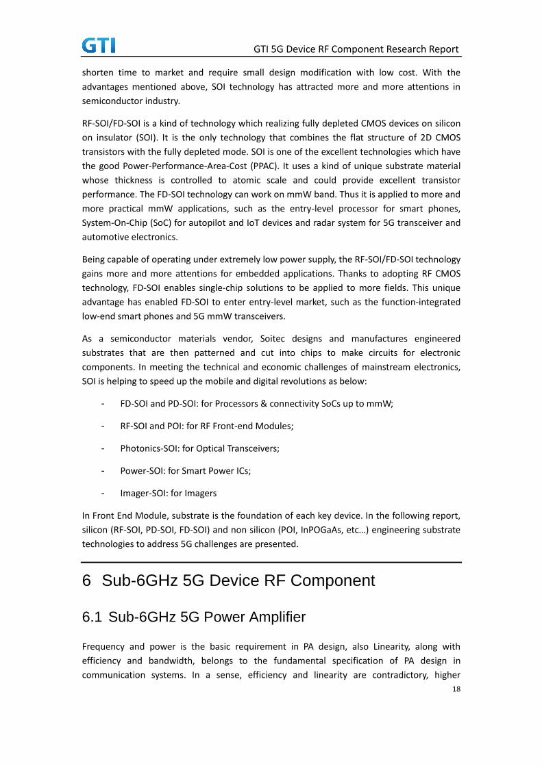
The performances and measurement results of 6-inch 2um GaAs HBT process are given in
table 6-2 and figure 6-8:
Table 6-2 Performances of 6-inch 2um GaAs HBT process
Parametre HiWafer
HBT02
GTI 5G Device RF Component Research Report
27
Beta(V) 120(@1kA/cm2) 75(@1kA/cm2)
BVcbo(V) 24(@2kA/cm2) 24(@2kA/cm2)
BVceo(V) 13(@2kA/cm2) 13(@2kA/cm2)
ft/fmax(GHz) 40/60 40/60
ResistorTaN(Ω/) 50 50
Capacitor(pF/mm2) 600/930 600/930
Au: M1/M2(μm) 1/2 1/2
The key parameters in table 6-2 are explained as follows:
Beta(β): current gain, the 75-Gian transistor is commonly used in 3G, the 120-Gain
transistor is commonly used in 4G and the later generations.
BVcbo, BVceo: the breakdown voltage, the higher breakdown voltage means higher
work voltage.
ft: current cut-off frequency. The higher the ft, the better frequency characteristics.
fmax: highest oscillation frequency, where the power gain of the transistor decreases to
1.
Figure 6-8 Measurement results of 6-inch 2um GaAs HBT process
GaAs device have the advantages of high electron mobility, low loss semi-insulating substrate,
high linearity, high cut-off frequency, and high breakdown voltage, making them superior to
CMOS in power performance. Therefore, GaAs device holds a dominant position in
performance advantages over CMOS in the 4G PA market. For the future 5G PA market, the
standard GaAs based modules will continue to maintain their advantages in power
performance. In the whole market, compared with the highly integrated CMOS device and
high power performance GaN device, GaAs device can continue to play its performance
advantages by increasing its level of integration through processing and packaging.
Considering the fact that GaAs and silicon-based devices are still able to meet the cost and
performance requirements. GaN device will not be used in 4G mobile phones for its still high
working voltage. However, with the development of GaN technology, GaN device may be
used in 5G mobile phone RF front-end module. Compared with high frequency devices such

GTI 5G Device RF Component Research Report
28
as GaAs and InP, the power density of GaN devices will be greater, which will help reducing
the chip area of the PA. Compared with LDCMOS and SiC, GaN has better frequency
characteristics; GaN device also has wider the instantaneous bandwidth, thus fewer
amplifiers are needed to cover all bands and channels. GaN device has many other
advantages, such as higher output impedance. High output impedance makes it easier for
impedance matching and power combining of GaN device, and to cover a wider frequency
range and improve the applicability of RF power amplifiers.
GaN applied in 5G phones, there are several problems need to be solved:
GaN devices work in low voltage.
The high thermal conductivity in cell phone
High cost
6.1.2.4 Existing Sub-6GHz 5G Power Amplifier Products
1. Measured Data of Sub-6GHz 5G NR PA
Currently, the RF front-end module that supports 3.3GHz-4.2GHz and 4.4GHz-5GHz for 5G
NR 3GPP standards is under develop, and a conceptual image of the fully technology
demonstrator for sub 6 GHz TDD systems in 3.5/4.5 GHz could look like this. Actual
Implementation is likely to vary, but the main concepts remain intact.
Figure 6-9 Block diagram of RFFE module support 3.3GHz-4.2GHzand 4.4GHz-5GHz
The PA in the sub-6 GHz module will be assumed to be LTE and 5G NR compatible. The PA
will have to be designed to support power class 2 HPUE in at least some sections of the band.
In general, Support for:

GTI 5G Device RF Component Research Report
29
LTE and 5GNR PC 3 and PC 2
CP-OFDM and DFT-s-OFDM waveforms
Full and Partial allocations (at channel edge and in-channel)
20MHz and 100MHz bandwidths
QPSK, 16QAM and 64QAM
Normal, clipped or low PAPR waveforms
As shown in figure 6-10, we use CP-OFDM QPSK Full RB waveform and 3.8V power supply, PA
Engine can achieve 26.9dBm@100MHz for -36dBc ACLR, almost same power capability is
maintained for 200MHz and 400MHz channel bandwidths.
Figure 6-10 ACLR test results based on MP PA engine
In figure 6-11, shows the corresponding changes of linearity and efficiency
Figure6-11 Efficiency and ACLR test results based on MP PA engine
PS: all the figures above are provided by Skyworks.

GTI 5G Device RF Component Research Report
30
2. Measured Data of Sub-6GHz 5G NR PA
Now according to 5G NR Standalone 3GPP specification, supporting Band n77 3.3GHz-4.2GHz
900MHz bandwidth RF front end module is already developed. The block diagram is in Figure
6-12
Figure 6-12 5G NR RF Front End Module Block Diagram
This RF Front End Module integrates power amplifier, Tx/Rx pass band filter, LNA, Switch and
coupler.
Supporting linear output power 24.5dBm (Power Class 3) at Ant port.
a) Supporting high PAR of ~9dB 5G CP-OFDM modulation
b) Supporting max CA bandwidth of 400MH, 4CC
c) Supporting QPSK/16QAM/64QAM modulation signal
d) Supporting 2dB max power back off to 22.5dBm (single carrier 100MHz
bandwidth and 64QAM modulation signal)
e) Supporting 3dB max power back off to 21.5dBm (4CC 400MHz bandwidth and
64QAM modulation signal)
f) Supporting APT technology
Detailed RF front end module measurement condition and data are as below:
a) Test Condition
• Linear 22.5dBm output power at Ant port
• CP-OFDM 5GNR input waveform
• Single carrier 100MHz bandwidth
• 64QAM modulation

GTI 5G Device RF Component Research Report
31
• 4.5V constant supply voltage
b) Test Data
The module Tx Gain from 3.3-4.2GHz 900MHz bandwidth is from 24-26dB
Figure 6-13 5G NR RF Module Gain data
RF Module power consumption based on different duty cycles.
Figure 6-14 5G NR RF Module power consumption based on different duty cycles
F Module ACLR within 3.3-4.2GHz is less than -36dBc.
100 % duty cycle ~ 615 mA
25 % duty cycle ~ 154 mA
40 % duty cycle ~ 246 mA

GTI 5G Device RF Component Research Report
32
Figure 6-15 5G NR RF Module ACLR
RF Module EVM within 3.3-4.2GHz is less than 3.5%.
Figure 6-16 5G NR RF Module EVM Data
Note: Above RF Module information and data are provided by Qorvo.
3. System Diagram of Sub-6GHz 5G NR PA
Vanchip is developing a 5G RFFEM (RF Front End Module) supporting 3.3GHz-4.2GHz. Figure
6-17 below is the system diagram.

GTI 5G Device RF Component Research Report
33
PA
LNA
SPDT Filter
PA
LNA
SPDT Filter
3.3GHz-4.2GHz
3.3GHz-4.2GHz
Solution A
Solution B
CPLANT
CPLANT
Figure 6-17 5G NR RF Front End Module Diagram
In Solution A, a 3.3GHz-4.2GHz PA, a coupler, a LNA (low noise amplifier) and SPDT switch are
integrated in a single module. Customers can place the filter on PCB to meet their
requirements on performance and cost.
In Solution B, filter is placed into the module to optimize the module performance and to
achieve the maximum integration for customers.
Both solutions support requirements as below:
a) PC2, PC3 in 5G NR and LTE
b) QPSK/16QAM/64QAM Modulation
c) CP-OFDM and DFT-s-OFDM Waveform
d) Maximum 400MHz 4 Carrier Aggregation
e) APT and ET
6.2 Sub-6GHz 5G Filter
6.2.1 Existing Mobile Device Commercial Filter
The rapid growth in mobile wireless data and 4G LTE networks has created an ever-increasing
requirement for new spectrum bands to accommodate wireless traffic. Whereas 3G
networks used only about five bands, there are already over 20 4G LTE bands and this
number could rise to more than 40 in the near future.
Though it’s not practical to support all worldwide bands in a single smartphone, a

GTI 5G Device RF Component Research Report
34
feature-rich model for international use may need to filter transmit and receive paths for 2G,
3G, and 4G in up to 15 bands, as well as Wi-Fi, Bluetooth, and global navigation satellite
system (GNSS). Such a phone may require as many as 30 to 40 filters. The situation is likely to
become even more complex with next-generation high-end smartphones requiring even
more filters.
6.2.1.1 Common Types of Filter
A filter removes unwanted frequency components from a signal while preserving desired
frequency components. There are four basic types of filters that accept or reject signals in
different ways (see Figure 6-18). The different types are defined as
Low pass: Allows all frequencies below a certain frequency to pass while rejecting all
others (opposite of high pass)
High pass: Allows all frequencies above a certain frequency to pass while rejecting all
others (opposite of low pass)
Band pass: Allows all frequencies between two frequencies to pass while rejecting all
others (opposite of band stop)
Band stop (or band reject): Rejects all frequencies between two frequencies while
passing all others (opposite of band pass)
Band stop and band reject filters are also known as notch filters.
Figure 6-18 Basic Filter Types
Filter construction varies by application, with size, cost, and performance the major variables.
Here are some example filter constructions:

GTI 5G Device RF Component Research Report
35
Discrete inductor-capacitor (LC) filters are low-cost structures of moderate performance
and size. The LC elements are sometimes implemented as printed structures on
substrates called an integrated passive device (IPD).
Multilayer ceramic filters are low to moderate cost and have similar performance to LC
filters. Their footprint is generally reasonable, but their thickness is becoming an issue
as mobile applications emphasize thinner and thinner designs.
Monoblock ceramic filters are much higher performance than multilayer ceramics and
also more expensive. They’re also physically larger and usually aren’t suitable for mobile
applications.
Acoustic filters have the capability to meet both low and high frequencies up to 6 GHz,
are small in size, and offer the best performance and cost for complex filter
requirements. Acoustic filters are the most common filter construction for mobile
devices.
Cavity filters are used in infrastructure applications only. They can achieve good
performance at reasonable cost but are large.
6.2.1.2 Key Parameters and Influence Factors
Filters can be designed to meet a variety of requirements. Although they use the same basic
circuit configurations, circuit values differ when the circuit is designed to meet different
criteria. In-band ripple, fastest transition to the ultimate roll-off, and highest out-of-band
rejection are some of the criteria that result in different circuit values. Filters allow only
particular frequencies or bands of frequencies to pass through and are, thus, an essential
tool for RF design engineers. Typical filter response curve is shown in Figure 6-19.
Figure 6-19 Typical Filter Response Curve
In case your knowledge of electronics is a bit rusty, here’s a brief tutorial on some of the
more important terms and concepts to help refresh your memory.

GTI 5G Device RF Component Research Report
36
1) Attenuation: An amplitude loss, usually measured in decibels (dB), incurred by a signal
after passing through an RF filter.
2) Cutoff: Normally taken to be the point at which the response of the filter has fallen by 3
dB.
3) Group delay: The derivative of a filter’s phase with respect to frequency. Group delay,
measured intime (in seconds), can be thought of as the propagation time delay of the
envelope of an amplitude modulated signal as it passes through an RF filter.
4) Insertion loss: Loss of signal power resulting from the insertion of a component.
5) Isolation: Separation of one signal from another to prevent unintentional interaction
between them (for example, transmit and receive interaction).
6) Q factor: The “quality” factor is a measure of the selectivity of a resonant circuit
described as the ratio of stored versus lost energy per oscillation cycle.
7) Passband: The region through which the signal passes relatively unattenuated.
8) Ripple: The variation of insertion loss in the passband.
9) Selectivity: A measurement of the capability of the filter to pass or reject specific
frequencies relative to the center frequency of the filter. Selectivity is usually stated as
the loss through a filter that occurs at some specified difference from the center
frequency of the filter.
10) Stopband: A band where the filter has reached its required out-ofband rejection,
defined as a required number of decibels.
The figure shows some clear trends:
1) Loss increases as the Q factor drops and increases more rapidly for lower values of
resonator Q.
2) The edges of the passband become more rounded and the passband narrower as the Q
decreases. Note how each successively lower Q plot fits inside the previous.
3) The loss at the passband edges increases more than loss in the middle of the band. This
poses a serious problem for modulations that go right to the edge of the passband.

GTI 5G Device RF Component Research Report
37
Fiture 6-20 Acoustic Filter Attentuation based on different Q
Narrow modulations such as GSM (200 kHz) and CDMA (1.25 MHz) will suffer the most
sensitivity loss at the band edge due to this effect, while WCDMA (3.84 MHz) will suffer less.
LTE results depend on the system bandwidth, with narrower bandwidths more affected.
6.2.1.3 Acoustic filter
Acoustic filter technologies continue to evolve to meet the challenges of the global transition
to 4G networks. In this chapter, you find out about surface acoustic wave (SAW) and bulk
acoustic wave (BAW) filter technologies, which are used to solve many of today’s toughest
mobile device filtering problems.
1) SAW: Mature But Still Growing
SAW filters are widely used in 2G and 3G receiver front ends, duplexers, and receive filters.
SAW filters combine low insertion loss with good rejection, can achieve broad bandwidths,
and are a tiny fraction of the size of traditional cavity and ceramic filters.
Because SAW filters are fabricated on wafers, they can be created in large volumes at low
cost. SAW technology also allows filters and duplexers for different bands to be integrated on
a single chip with little or no additional fabrication steps.
The piezoelectric effect that exists in crystals with a certain symmetry is the ‘motor’ as well
as the ‘generator’ in acoustic filters. When you apply a voltage to such a crystal, it will
deform mechanically, converting electrical energy into mechanical energy. The opposite
occurs when such a crystal is mechanically compressed or expanded. Charges form on
opposite faces of the crystalline structure, causing a current to flow in the devices and/or
voltage between the devices. This conversion between electrical and mechanical domains
happens with extremely low energy loss, achieving exceptional efficiency inboth directions.
In solid materials, alternating mechanical deformation createsacoustic waves that travel at
velocities of 3,000 to 12,000 meters per second. In acoustic filters, the waves are confined to

GTI 5G Device RF Component Research Report
38
create standing waves with extremely high-quality (high-Q) factors of several thousand.
These high-Q resonances are the basis of the frequency selectivity and low loss that acoustic
filters achieve.
In a basic SAW filter (see Figure 6-21), an electrical input signal is converted to an acoustic
wave by interleaved metal interdigital transducers (IDTs) created on a piezoelectric substrate,
such as quartz, lithium tantalite (LiTaO3), or lithium niobate (LiNbO3). Its slow velocity makes
it possible to fit many wavelengths across the IDTs in a very small device.
Figure 6-21 SAW Filter Architecture
A key advantage of SAW is its capability to optimally meet standard filter applications up to
1.9 GHz, including several standard bands such as GSM, CDMA, 3G, and some 4G bands.
Additionally, techniques such as wafer level packaging (discussed in Chapter 6) are being
used to shrink SAW filters, allowing the integration of filters and duplexers for multiple bands
onto a single chip. This is becoming increasingly important as smartphones incorporate more
functions.
SAW filters, however, have limitations. Above about 1 GHz, their selectivity declines, at about
2.5 GHz.
The use of SAW is limited to applications with modest performance requirements SAW is also
very temperature sensitive, this issue is better handled by temperature compensated SAW
technology (TC-SAW). The stiffness of the substrate material tends to decrease at higher
temperatures and acoustic velocity diminishes. A SAW filter’s response may shift downward
by as much as 4 MHz as temperature increases. This limitation has become more significant
as guard bands become narrower and consumer devices are specified to operate across a
wide temperature range (typically, –20°C to 85°C).
2) BAW: High Performance
BAW filters generally deliver superior performance (higher Q) with lower insertion loss at
higher frequency levels. With BAW technology, it is possible to create narrowband filters
with exceptionally steep filter skirts and excellent rejection. This makes BAW the technology
of choice for many challenging interference problems. BAW delivers these benefits at

GTI 5G Device RF Component Research Report
39
frequencies above 1.5 GHz, making it a complementary technology to SAW (which is most
effective at lower frequencies). BAW can address frequencies up to 6 GHz and is used for
many of the new LTE bands above 1.9 GHz. BAW is also highly effective for LTE/Wi-Fi
coexistence filters.
BAW filter size also decreases with higher frequencies, which makes these filters ideal for the
most demanding 3G and 4G applications. In addition, BAW design is far less sensitive to
temperature variation even at broad bandwidths.
Unlike SAW filters, the acoustic wave in a BAW filter propagates vertically (see Figure 6-22).
In a BAW resonator using a quartz crystal as the substrate, metal patches on the top and
bottom sides of the quartz excite the acoustic waves, which bounce from the top to the
bottom surface to form a standing acoustic wave. The frequency at which resonance occurs
is determined by the thickness of the slab and the mass of the electrodes. At the high
frequencies in which BAW filters are effective, the piezo layer must be only micrometers
thick, requiring the resonator structure to be made using thin-film deposition and
micro-machining on a carrier substrate.
Fiture 6-22 BAW Filter Architecture
To keep the waves from escaping into the substrate, an acoustic Bragg reflector is created by
stacking thin layers of alternating stiffness and density. The result of this approach is called a
solidly mounted resonator BAW (BAW-SMR). A Bragg reflector is a structure formed from
multiple layers of alternating materials with varying refractive index.
An alternative approach, called a film bulk acoustic resonator (FBAR), etches a cavity
underneath the active area, creating suspended membranes. Figure 6-23 compares
BAW-SMR and FBAR filter designs.

GTI 5G Device RF Component Research Report
40
Figure 6-23 FBAR Vs BAW-SMR Architecture
Both types of BAW filters can achieve very low loss because the density of their acoustic
energy is very high and the structures trap acoustic waves very well. Their achievable Q is
higher than any other type of filter of reasonable size employed at microwave frequencies:
2,500 at 2 GHz. This results in superb rejection and insertion loss performance, even at the
critical pass band edges.
The fundamental difference between FBAR and BAW-SMR is in how acoustic energy is
trapped. For FBAR, the air/crystal interface on both faces of the resonator ensures that the
main mode of interest is appropriately trapped. In BAW-SMR, Bragg reflectors underneath
the resonator effectively trap this mode. Another major difference between FBAR and
BAW-SMR is the thermal path for heat generated in the device. In BAW-SMR, the heat has a
conduction path into the substrate from which it can be spread. In FBAR, because there is an
air gap on each side of the resonator, the thermal conduction path is weaker.
Because BAW filters offer low insertion loss, they help compensate for the higher losses
associated with the need to support many bands in a single smartphone. Besides improving
signal reception, lower loss also contributes to longer battery life. BAW excels in applications
where the uplink and downlink separation is minimal and when attenuation is required in
tightly packed adjacent bands.

GTI 5G Device RF Component Research Report
41
Figure 6-24 2G/3G/4G Filter Technology from Qorvo
6.2.2 3.3GHz-4.2GHz 5G Filter Design
6.2.2.1 Design Challenges
Upcoming RF architecture for 5G to be introduced in 2020 and beyond would further require
higher frequency and wider frequency bandwidth as it is being standardized under 3GPP
Release 15. Filtering devices would be required to cover rather much higher relative
bandwidth ratio as opposed to current 4G requirement as well as the compatibilities to HPUE
requirement which is considered to be standardized within Release 15 while filtering devices
are expected to provide rather lower insertion loss as well as decent attenuation level.
Furthermore, when initial 5G implementation is done by NSA (Non-Standalone) mode, this
may possibly generate IMD issue which would require filtering devices to provide lower
passive inter-modulation characteristics. Therefore, upcoming new filtering RF devices must
consider satisfying these potential issues.
6.2.2.2 Alternative Processes
Combine with 6.2.1.3 introduction of SAW filter, as the following chart 6-25, at the present
the technology of filters have been divided to 3 series: ONE is SAW technology, it has always
been utilized for main bands of cellular phone standard and this should continue to be the
case as 5G will be using existing LTE bands after refarming by 3GPP. But it is difficult to meet
the requirement of 5G high frequency and wider frequency bandwidth; TWO is FBAR/BAW
technology, it has mainly been utilized for satisfying rather stringent attenuation and
somewhat higher frequency requirement especially for the solution of coexistence with

GTI 5G Device RF Component Research Report
42
adjacent systems. This technology is capable of covering up to approximately 3800MHz
ranges while the company has been working to push the envelope toward even much higher
frequency ranges especially to satisfy upcoming 5G requirement. THREE is LTCC (Low
Temperature Co-fired Ceramic) technology. It is capable of meeting wider frequency
bandwidth and higher frequency requirement. Similar to LTCC, LC structures on IPD
technology, while a bit lower Q, are essential for integration in modules covering PA, switch,
LNA and filters for frequencies above 3.3GHz, thanks to its miniaturization capabilities.
Figure 6-25 Common Filter Technologies
6.2.2.3 Existing 3.3GHz-4.2GHz 5G Filter Products
1) Technological advantages of multilayer ceramic filters (LTCC)
With the utilization of multilayer ceramic technologies, it can provide extremely low
insertion loss for Sub-6GHz while covering entire required bandwidth. The relative
bandwidth that can be covered with multilayer ceramic filters is approximately from 5 to
50%. It also contributes to the downsizing and lower profile requirements with significantly
stable performance and relatively low cost. This technology also provides rather high
power handling capabilities in comparison with SAW technologies and this should be
another advantage as HPUE should be required by 5G Sub-6GHz standard. On the other hand,
multilayer ceramic filters provide rather relaxed skirt characteristics as opposed to SAW filter
technology. This concept should directly be applied to 5G Sub-6GHz requirement including
Band n77, n78 and n79.
At the present, there is 5G LTCC filter already can support the HPUE device of Band n77 and
Band n78, the main performance has been showed at below sheets and Table 6-3, Figure
6-26, Figure 6-4, Figure 6-27.

GTI 5G Device RF Component Research Report
43
Table 6-3 Multilayer Ceramic Band Pass Filter for 5G NR Sub-6GHz Band n77 HPUE
Pass band Frequency 3.3GHz – 4.2GHz
Insertion Loss(Type) 1.29dB
Attenuation(Type)
600-2700MHz 44.4dB
4900-5900MHz 32.4dB
6600-8400MHz 44.1dB
9900-12600MHz 32.4dB
Power Capability +33dBm at pass band frequency,10000Hr
Size 2.0mm x 1.25mm x 0.65mm MAX,LGA Package
Figure 6-26 Frequency performance of LTCC BPF for 5G NR Sub-6GHz Band n77 HPUE
Note: Above actual test data is provided by TAIYO YUDEN.
Table 6-4 Multilayer Ceramic Band Pass Filter for 5G NR Sub-6GHz Band n78 HPUE
Pass band Frequency 3.3GHz – 3.8GHz
Insertion Loss(Type) 1.54dB
Attenuation(Type)
600-2700MHz 46.5dB
4900-5900MHz 39.2dB
6600-8400MHz 42.6dB
9900-12600MHz 37.6dB
Power Capability +33dBm at pass band frequency,10000Hr
Size 2.0mm x 1.25mm x 0.65mm MAX,LGA Package
-60
-50
-40
-30
-20
-10
0
0 2000 4000 6000 8000 10000 12000 14000 16000 18000
Attenuation[dB]
Frequency[MHz]
S11
S21

GTI 5G Device RF Component Research Report
44
Figure 6-27 Frequency Performance of LTCC BPF for 5G NR Sub-6GHz Band n77 HPUE
Note: Above simulation data is provided by TAIYO YUDEN.
2) Integrated n77 filte
Below is integrated filter supporting 5G Band n77
Figure 6-28 n77/n78 5G RF FEM Block Diagram
Tx chain gain data is as below
-60
-50
-40
-30
-20
-10
0
0 2000 4000 6000 8000 10000 12000 14000 16000 18000
Attenuation[dB]
Frequency[MHz]
S11
S21

GTI 5G Device RF Component Research Report
45
Figure 6-29 RF FEM Tx Gain Data
6.2.3 4.4GHz-5GHz 5G Filter Design
6.2.3.1 Design Challenges
3GPP RAN4 members have come to the agreement to choose the band from 4.4GHz to
4.99GHz earlier, on the other hand, as China MIIT (Ministry of Industry and Information
Technology) published additional frequency ranges for 5G trial, including 4.8-5GHz. This
was also proposed within 3GPP RAN4 and it has been approved that the upper edge of Band
n79 was extended from 4.99GHz to 5GHz to support the spectrum demand in China. Within
3GPP, Band “n79” was newly assigned for “4.4-5GHz”. Same as the filter for sub-6GHz 5G NR,
the filters for 4.4-5GHz need to support wider frequency bandwidth and higher frequency.
Other technology or integrated technologies shall be utilized depending upon the
attenuation requirement of adjacent systems such as WiFi 5GHz and/or LAA/eLAA which
starts at 5.15GHz.
6.2.3.2 Alternative Processes
Same as 6.2.2.2, LTCC technology is capable of meeting wider frequency bandwidth and
higher frequency requirement.
6.2.3.3 Existing 4.4GHz-5GHz 5G Filter Products
1. Introduction of LTCC filter and related performance
Technology background of this Band n79 LTCC filter is same as previously explained in the
article of Band n77 filter. LTCC based filter design is rather flexible and the design can be
applied to other type devices including low pass filter, band pass filter, diplexer for Sub-6GHz
in the light of upcoming 5G requirement. At present, Taiyo Yuden has been working on series
of different band pass filters for 5G Band n79 and the following is the example from the
variations and the size is 2.0mm x 1.25mm x 0.65mm Max with LGA (Land Grid Array)
package and performance is as shown as below Table 6-5, Figure 6-30.

GTI 5G Device RF Component Research Report
46
Table 6-5 Multilayer Ceramic Band Pass Filter for Sub-6GHz 5G NR Band n79 HPUE
Pass band Frequency 4.4GHz – 5GHz
Insertion Loss(Type) 2.09dB
Attenuation(Type)
100-915MHz 54.0dB
1427.9-1467MHz 50.7dB
2495-2690MHz 50.9dB
5490-5925MHz 31.2dB
Power Capability +33dBm at pass band frequency, 10000Hr
Size 2.0mm x 1.25mm x 0.65mm MAX, LGA Package
Figure 6-30 Frequency Performance of LTCC BPF for Sub-6GHz 5G NR Band n79 HPUE
Note: Above simulation data is provided by TAIYO YUDEN.
2. Integrated n79 filter
5G bands have higher frequency and wider band width, which requires filters provide more
steep conversion bandwidth, these new requirements and characteristics bring great
challenges to the existing acoustics based filters. The integrated passive filter which can be
used in N79 device design provides a balance in performance, size and cost. Integrated n79
filter is still under development.
6.3 Sub-6GHz 5G Low Noise Amplifier
6.3.1 Existing Mobile Device Commercial Low Noise Amplifier
Products
Broadband LNA is a critical component in radar, communication, electronic countermeasures,
telemetry and remote areas. In wireless communication, the higher data transmission speed
-60
-50
-40
-30
-20
-10
0
0 2000 4000 6000 8000 10000 12000 14000 16000 18000
Attenuation[dB]
Frequency[MHz]
S11
S21

GTI 5G Device RF Component Research Report
47
requires the higher of channel capacity. For RF receiver, the noise figure and linearity of LNA
directly affects and decides the sensitivity and dynamic range of a RF receiver, which requires
LNA’s low noise to improve the sensitivity and power gain, to reduce the noise of next level
circuit.
6.3.2 Sub-6GHz 5G Low Noise Amplifier Design
6.3.2.1 Design Challenges
Wideband LNA design challenges are to keep high gain, low noise finger and high IP3 in the
full band.
6.3.2.2 Alternative Processes
The processes for LNA include GaAs pHEMT, SiGe HBT and CMOS. SiGe HBT and CMOS with
good compatibility and low cost, GaAs pHEMT has excellent noise and gain performance.
GaAs pHEMT (E-mode) has the 2-D characteristic of the heterojunction, in order to get high
carrier mobility and low noise figure.
1) 0.15um E-mode GaAs pHEMT
(E-mode) 0.15um GaAs pHEMT (E-mode) contains 17 masks and over 200 process steps. Each
of these steps needs repeatable experiment, to ensure the whole process reliable and
commercial
The domestic foundries are developing 6-inch 0.15um GaAs pHEMT technology, one choice
of 5G’s PA. The main performances of this technology are given in table 6-6.
Table 6-6 main performances of 6-inch 0.15um GaAs pHEMT technology
Item Unit Performance Condition
TFR ohm/sq 50+/-5
Lg um 0.150 +/- 0.02
Rs (Epi) ohm/sq 150 +/- 20
Idss mA/mm <0.05 @Vgs=0V Vds=1.5V
Gm max mS/mm 1000 +/-150
Imax mA/mm 420 +/- 100 @Vgs=+0.9V
Vp V 0.3 +/- 0.15 @1mA/mm
BVgd V 10 +/- 3 @1mA/mm
ft GHz 110+/-25
Psat mW/mm > 700 mW/mm @29 GHz
The key parameters in table 6-6 are explained as follow:
TFR: thin film resistor, produced by TaN.
Lg: gate length, the smaller Lg , the higher Ft.

GTI 5G Device RF Component Research Report
48
Rs(Epi): epitaxy active layer resistor.
Idss: the drain current.
Gm_max: the maximum value of the transconductance.
Idmax: the maximum value of the drain current.
Vp: the gate threshold voltage. The gate voltage is larger than Vp, the transistor is
switched on;the gate voltage is smaller than Vp, the transistor is switched off.
BVgd: the drain-source breakdown voltage.
ft: the cut off frequency.
2)0.25um E-mode GaAs pHEMT
The domestic foundries have their own IP on 0.25um GaAs pHEMT process technology,
include material, device, integration, producing process, yield control, modeling and process
design kit(PDK). 0.25um GaAs pHEMT technology has been finished and reached the mean
level of the industry.
0.25um GaAs pHEMT is applied for LNA and PA. And also provides E/D mode logic devices,
0.5um GaAs pHEMT (D-mode) for switch, ESD devices, resistor and capacitor.
Table 6-7 The main performances of the 0.25um GaAs pHEMT technology
Item Unit Performance Condition
Idss mA/mm <0.01 @Vgs=0V
GM_max_E mS/mm 800±100
I_max_E mA/mm 500±80 @Vgs=+1.4V
Vp_E V 0.3±0.15 @1mA/mm
BVgd_E V 12±4 @1mA/mm
ft_E GHz 75±15
Psat mW/mm >370 @10 GHz
The key parameters in table 6-7 are explained as follow:
Idss: the drain current.
Gm_max_E: the maximum value of the transconductance.
Idmax: the maximum value of the drain current.
Vp_E: the gate threshold voltage,.
BVgd_E: the drain-source breakdown voltage.
ft_E: the cut off frequency.
In addition to above mentioned technologies, the existing SOI technology could also provide
designers a cost-optimized platform to improve PPAC of LNA. With the help of SOI

GTI 5G Device RF Component Research Report
49
technology, LNAs can be realized in the RF front end modules of 4G and sub-6G 5G
components.
6.3.2.3 Existing Sub-6 5G Low Noise Amplifier Products
LNA is integrated into module design as below to support n77 3.3-4.2GHz.
Figure 6-31 Band n77 LNA in RF FEM
7 mmWave 5G Device RF Component
7.1 mmWave 5G Power Amplifier
RF PA plays a very important role in wireless communication system. With the development
of communication technology, the requirement of RF PA is increasing, especially for
broadband, high linearity and high efficiency. While amplifying the signal, PA must reduce
the distortion of the signal as much as possible. Therefore, linearity is a very important index
in the design of the power amplifier, and other indexes include gain, flatness, efficiency,
distortion and so on. GaAs E-mode pHEMT technology inherits many advantages of D-mode
pHEMT technology, and has the characteristics of single power, high span and high linearity.
The current development trend of the mobile phone market has been extending the time of
call and improving the function of the mobile phone so that it needs to keep enough
performance to reduce the voltage. The E-mode pHEMT device has a very low switching
voltage, so there is no limit on the offset margin.
1) 0.15um E-mode pHEMT
(E-mode) 0.15um GaAs pHEMT contains 17 masks and over 200 process steps. Each of these
steps needs repeatable experiment, to ensure the whole process reliable and commercial
The domestic foundries are developing 6-inch 0.15um GaAs pHEMT technology, one choice
of 5G’s PA. The main performances of this technology are given in table 7-1.
Table 7-1 main performances of 6-inch 0.15um GaAs pHEMT technology
Item Unit Performance Condition
TFR ohm/sq 50+/-5
Lg um 0.150 +/- 0.02
Rs (Epi) ohm/sq 150 +/- 20
Idss mA/mm <0.05 @Vgs=0V Vds=1.5V
Gm max mS/mm 1000 +/-150

GTI 5G Device RF Component Research Report
50
Imax mA/mm 420 +/- 100 @Vgs=+0.9V
Vp V 0.3 +/- 0.15 @1mA/mm
BVgd V 10 +/- 3 @1mA/mm
ft GHz 110+/-25
Psat mW/mm > 700 mW/mm @29 GHz
TFR: thin film resistor, produced by TaN.
Lg: gate length, the smaller Lg, the higher Ft.
Rs(Epi): epitaxy active layer resistor.
Idss: the drain current.
Gm_max: the maximum value of the transconductance.
Idmax: the maximum value of the drain current.
Vp: the gate threshold voltage.the gate voltage is larger than Vp, the transistor is
switched on;the gate voltage is smaller than Vp, the transistor is switched off.
BVgd: the drain-source breakdown voltage.
ft: the cut off frequency.
2) InP
Currently, GaAs device has dominated most of the market because of its mature technology
in the microwave frequency band. However, InP device has higher breakdown voltage, higher
average electron velocity, larger discontinuity in the bandgap at the interface of
InAlAs/InGaAs heterojunction, higher 2DEG concentration, and higher electron mobility in
channel, making it more suitable for high frequency applications.
For low voltage applications, InP HBT is expected to replace GaAs HBT. InP HBT is made of
narrow bandgap material InGaAs. The bias voltage is as low as 0.5V~0.6V. In addition, InP
HBT also exhibits better heat conduction characteristics, better heat dissipation capability
(about 1.5 times of GaAs substrate) and higher peak electron velocity, allowing higher
performance at lower voltages.
Although InP/InGaAs HBT with lattice matching on the InP substrate has superior high
frequency and high speed characteristics, and lower turn-on voltage than GaAs HBT, it suffers
from small substrate size, high cost, and fragility of the InP substrate, limiting its large-scale
and low lost production. The capability to obtain high quality and large size semi-insulating
InP substrate is key to lower cost. Therefore, to meet the ever increasing demand of InP
devices, fundamental task is to grow high quality and large diameter InP single crystal
substrate.
3) GaAs mHEMT
Benefiting from the cost, fragility and process compatibility issues of InP substrate, more and

GTI 5G Device RF Component Research Report
51
more research on GaAs mHEMT technology has been conducted. GaAs mHEMT technology is
to grow a relatively thick InAlAs layer between the channel and the GaAs substrate. The
composition of In changes from a certain value X to 0, so the mismatch of the lattice is
alleviated. After the adding of a buffer layer with graded component, the component X of In
in the channel layer can be chosen almost arbitrarily between 30%~60%, and the device
performance is optimized with a great degree of freedom. mHEMT can be considered as InP
HEMT technology on GaAs substrate. It shows superior performance to InP in terms of low
noise, allowing GaAs to solidify its position at the low-end of millimeter wave, and further its
way into the high-end territory of millimeter wave.
In 2008, 220GHz-320GHz mHEMT MMIC amplifier was reported using high In composition in
InGaAs as channel to achieve high carrier density and mobility. Double InAlAs barrier layers
and bilateral delta doping are designed to increase channel electron confinement and reduce
contact resistance, and the buffer layer with linear component change is used to achieve
lattice matching. The Ft and Fmax are 515GHz and 700GHz, respectively, for the device with
35nm gate length and 20um gate width. The linear gain of the two stage amplifier is more
than 10.5 dB in the 220GHz-320GHz frequency band, and the small signal gain is 13.5dB at
330GHz. In 2011, the device with 20nm gate length was reported, and the Ft was 660GHz for
the mHEMT with 2*10um gate width. GaAs mHEMT has been able to work into the H band
and enter the low-end of the terahertz. It has become an important component of the
sub-millimeter wave application, with a cost advantage.
Chapter 4.1 data sources: Hiwafer.
7.2 mmWave 5G Filter
mmWave devices are supposed to have large-scale and high density distribution to meet the
requirements of multi frequency and high frequency characteristics, which is bound to bring
an explosive growth of mmWave filter.
1) SAW filter
Under the existing framework, the SAW filter is the main force of 2G, 3G and 4G
communication technologies, and has the advantages of high design flexibility, good
frequency selection characteristics and small size, and can adopt the same production
process as the integrated circuit. The frequency characteristic of the SAW filter is closely
related to the pitch of the IDT electrode. The higher the frequency, the smaller the distance
between the electrodes is required. In fact, the spacing is not too small. The SAW filter drops
rapidly after the frequency exceeds 2.5 GHz. Therefore, the SAW filter is mostly used below
2.5 GHz.
2) BAW filter
Beyond 2.5GHz, BAW began to show the advantage. Compared to SAW, it is insensitive to
temperature changes, with low insertion loss and high out-of-band rejection, making its
share of 3G / 4G smartphones grow rapidly. However, most BAWs are used below 6 GHz and

GTI 5G Device RF Component Research Report
52
can reach a maximum of 20 GHz, which is applicable to 5 GHz systems below 6 GHz and can’t
be applied in the 5 GHz frequency band yet.
3) MEMS filter
Millimeter wave MEMS filter on the semiconductor substrate, the use of semiconductor
manufacturing process constitutes a filter structure, with high Q and low loss characteristics,
in the millimeter band has good performance. However, whether it is using gallium arsenide
substrate or silicon substrate, the cost is relatively high. Under the conditions of ensuring a
high degree of consistency, mass production is still more difficult.
4) Semiconductor chip filter based on MMIC process
The semiconductor chip filter based on the MMIC process can be integrated with the 5G
system chip or integrated with the microwave multi-chip module. At the same time, due to
the adoption of the semiconductor process, the batch consistency of the electric
performance is good, and the application is suitable for large-scale applications. Of course,
due to its circuit form can only be integrated by plane, the circuit transmission waveform for
the quasi-TEM wave inevitably surface waves, space radiation, dielectric and metal loss and
other natural defects.
The domestic foundry has developed GaAs IPD process for the passive circuit design. The
typical parameters of GaAs IPD process are given in Table 7-2.
Table 7-2 The typical parameters of GaAs IPD process
Typical parameters
Metal layer Metal 1:1 μm
Metal 2:2μm or 4μm
Metal1-metal2 Via PBO or Air-bridge
MIM capacitance density 300pF/mm2 or other
TaN thin film resistor 50Ω/
Inductor High Q
Background via diameter 40μm
passivation SiN or PBO
Wafer thickness 100 or 75μm
The LC low-pass filter and high-pass filter MMICs made by IPD process have covered 2-20GHz
in 0.5GHz step, the typical MMIC area is 1mm*0.75mm*0.1mm with a insert loss of 2dB.
Moreover, there are many customized band-pass filter products. The table 7-3 gives a typical
27.5GHz~29.5GHz high Q band-pass filter.
Table 7-3 The performances of a typical 27.5GHz~29.5GHz high Q band-pass filter
27.5GHz-29.5GHz band-pass filter
Central frequency:28.5GHz;
Band width:2000MHz;

GTI 5G Device RF Component Research Report
53
Insert loss:≤ 3 dB;
In-band flatness: ≤1 dB (Fluctuation range<1dB for any 1GHz,and<0.5dB for any
500MHz;
Input/output return loss: ≥13dB;
Out-band compression:70dBc@<6GHz
50dBc@6~20GHz
35dBc@20~26GHz
30dBc@31~34GHz
37dBc@34~40GHz
30dBc@>40GHz
Group delay flatness: ≤5ns@25
Area:5.2mm ×2mm ×0.1mm
The data in chapter 7.2 come from HiWafer
7.3 mmWave 5G Low Noise Amplifier
The research of MMwave LNA, abroad companies start very early, some companies had
made good samples or products. The international semiconductor companies such as
M/A-COM、Hittite、Qorve、TRW and UMS develop various kinds of MMwave LNA and have
got many achievements. Compared with these companies, the domestic research Started
relatively late. Haoquan Hu in University of Electronic Science and Technology of China
developed a Ka LNA with a 4.5dB noise figure and 20dB gain in 2006. A group in
Microelectronics Institute of the Chinese Academy of Sciences developed a 4-stage MMIC
LNA in 2007, which works in 26.5-36GHz with a 3dB noise figure and 20dB gain. In 2008, the
Shanghai Institute of Microsystem and Information Technology of Chinese Academy of
Sciences developed a 4-stage LNA using 0.15um GaAs pHEMT process, the LNA has a
18+/-1.5dB gain, an input VSWR smaller than 3, an output VSWR smaller than 2.3, DC power
of 96mW in 45GHz-65GHz. In 2008, the 38th institute of CETC developed a X-band 3-stage
LNA using negative feedback technology based on the 0.25um GaAs pHMET process of UMS,
this LNA has a 29.5dB gain with a noise figure below 1.7dB.
GaAs pHEMT has excellent noise and linearity performance. Owning to its high insulation
rate, GaAs substrate leads to the improvement of chip inductor quality factor (Q), which
helps to reduce the overall noise figure of the terminal. GaAs pHEMT has excellent noise and
gain performance, and has not been widely used in the early years due to price. Now, with
the progress of the process, GaAs pHEMT has become the mainstream for the development
of LNA. For cost and performance considerations, the mainstream process is the gate length
of 0.25um. GaAs pHEMT has implemented the gate length 0.1um level. For example, the
noise and gain of the PH10 process developed by UMS in Europe is 1.3dB and 7dB at 40GHz.
LNA developed by Qorvo in USA is 0.13um gate long, cut-off frequency of 110GHz with
TQP13 technology, and the noise figure at X frequency band is lower than 0.5dB.The
Thirteenth and Fifty-fifth Research Institute of China Electronic Science and Technology
Group and also developed 4 inch, 0.1um gate length pHEMT technology for high

GTI 5G Device RF Component Research Report
54
performance LNA. At present, Hiwafer are also actively developing the 6 inch, 0.15um gate
length GaAs pHEMT technology, the development of single process has been completed, and
it is in the stage of integration testing.
Chapter 4.4 data sources: Hiwafer
7.4 Switches for mmWave
Switches, the smallest active electronic components, play a critical role in the overall
performance and effectiveness of wireless communication systems. Switches route the
transmit and receive signals at different frequencies, enable monitoring and calibration and
are the base component for functions such as phase shifting and step attenuation. 5G, the
fifth generation wireless system, will continue this reliance on solid-state switching. But with
5G on the horizon, what are the switching requirements, and what makes a “great” 5G
switch? This chapter will explore a few basic specifications for 5G switching, discuss the use
of SOI technology and showcase a few critical functions for switches in 5G communications
systems.
7.4.1 What makes a ‘Great’ 5G Switch?
Switch performance is evaluated by a number of different specifications. In general, a “good”
switch has low insertion loss, high linearity, high port-to-port isolation, high power handling
and a fast switching time. In massive-MIMO architectures, each frequency bucket, sub-6 GHz
and mmWave, will stress each of these parameters.
In mmWave systems, broadband frequency operation becomes increasingly important. To
ease the transition to mmWave, switches must be able to support multiple bands, such as
dual bands (28 GHz and 39 GHz), or even triple bands (28 GHz, 39 GHz and 66 GHz). In
addition to multiple bands, each band has rigorous requirements on frequency-response
variation. For example, a 28 GHz mmWave application will have a wide bandwidth, and the
system gain can have a problem not meeting the flatness of the waveform over the wide
bandwidth. Real wideband support implies minimum variation across the supported
frequency band.
Due to the complexity of 5G system architectures, outstanding RF switch operation is critical
to enabling the new generation of devices. Specifications such as insertion loss, high linearity
and fast switching time are paramount to system performance.
1) Insertion Loss
Low insertion loss enables lower power amplifier drive, and thus lower energy
consumption and higher output efficiency.
2) Linearity
High linearity lends itself to support higher order modulation schemes without signal

GTI 5G Device RF Component Research Report
55
degradation. One measurement of a switch’s linearity is the third-order intercept point
(IP3). A high IP3 means the device will add minimal distortion in the form of
intermodulation and increased adjacent channel leakage ratio (ACLR) to the transferred
signal, and it will be able to withstand more extreme blocker conditions.
3) Switching time
Comparing with LTE and sub-6GHz system, mmWave systems require faster switching to
meet the requirements of the standard.
4) Power consumption and size
In mmWave system, the switch’s size and power consumption are two other key factors
in emerging massive-MIMO systems. As the name indicates, massive MIMO adds RF and
antenna content to the base station. Switches must be compact and feature low-power
consumption to be considered for use in massive-MIMO systems.
7.4.2 SOI Technology for 5G Switching
While many semiconductor technologies yield good active devices, very few yield good
switches. Silicon on insulator (SOI) is one semiconductor technology that has demonstrated
its effectiveness in switching.
CMOS is recognized for its manufacturing repeatability, which reduces end-product
performance variability. SOI technology leverages the economic benefit of a mainstream
complementary CMOS process to deliver a number of benefits, including manufacturability,
performance and integration. In regard to switch performance, SOI technology delivers low
insertion loss, high isolation and high linearity. In addition, SOI has the ability to integrate
analog, digital and mixed-signal capabilities on a single chip. Integration of mm-wave PA,
LNA, phase shifters and up/down mixers have also been achieved using fine geometry SOI
(45nm), making such technology a good candidate for fully integrated Transmit/Receive
phase arrays for 5G NR above 24GHz. This superior level of integration results in a smaller
form factor, higher flexibility/configurability, higher reliability and better system
performance.
8 Related ‘Black Technologies’
8.1 Engineered Substrate
8.1.1 What is 'Engineered Substrate'?
Engineered substrate defines a material most of the time dedicated to semiconductor
industry which is commonly made out of multiple raw materials. Its position in the supply

GTI 5G Device RF Component Research Report
56
chain is presented in figure below (Figure 8-1).
Figure 8-1 Engineering substrate in the supply chain, Soitec
Silicon On Insulator (SOI) is the most popular Engineered Substrate. It represents 6% of the
silicon substrates industry and forecast to enjoy high growth. Compound materials market
value is around 2%.
Figure 8-2 SOI substrate market in silicon substrates industry, Soitec
SOI history started 40 years ago. CMOS SOI was initially adopted in 1980’s in space
applications for its radiation hard properties. In 1998, IBM adopts SOI in large scale for its
mainframe processors ‘Power Cell’ powering its Power PC, followed by Apple which did
choose Motorola SOI processor for its G4 power station. Graphics processors derivatives
were then designed on SOI for well known game console PS3, Wii and X-Box. At the same

GTI 5G Device RF Component Research Report
57
time, AMD did develop all its product line micro processor on SOI (Athlon, Turion,
Opterion ….) moving SOI to high volume manufacturing using state of the art CMOS 300mm
foundries. In 2000’s, Philips Semiconductors was the second major adopter of SOI for its high
voltage IVN (In Vehicle Networking) transceivers. In the last ten years, more and more
applications are using SOI substrate as presented in following parts.
8.1.2 Why do we need 'Engineered Substrate'?
Engineered substrates are today at the heart of the RF Front End Module. CMOS bulk is not
much used till lossles and source of distortions. Future generations’ phone will use even
more SOI as SOI may find its way in transceivers RFIC and beyond.
Figure 8-3 Types of substrates in mobile phone, CMCC
There are two main motivations for China Mobile and end application leading companies to
learn about Engineered Substrate:
Awareness about new technologies in term of competitive advantage, supply chain.
There are many players between end users and engineered substrate suppliers due
to the supply chain complexity. Those players have not the expertise to give proper
visibility to end users and could hide unintentionally key information or even hide
engineered substrate as an option of differentiation;

GTI 5G Device RF Component Research Report
58
Figure 8-4 Cellular device industry chain, CMCC
Shorten time to market of new technology introduction. Sooner end user
understands the value of a new technology and faster he will enable it in its
application. In some case, decision can be taken to shorten supply chain by making a
vertical integration to limit the number of interfaces and then get closer to
engineered substrate suppliers. Leading SmartPhone companies are moving in this
direction and are making themselves some key differentiating parts of their product.
As an example, the automotive industry is actively working to enable new
technologies defined in reference technology roadmaps one year after its market
introduction and not three years as it is today. SmartPhone industry is a benchmark
for automotive industry in that respect.
RF-SOI is today in 100% of SmartPhone with growing content at each generation
whereas it wasn’t even introduced in this market in 2011.
Figure 8-5 RF-SOI content in Smartphone, Soitec
Looking at 5G, substrate technologies choice for RF is a key topic as presented in Skyworks

GTI 5G Device RF Component Research Report
59
reference white paper (Figure 8-6). SOI is clearly the preferred technology in most of key RF
building blocks.
Figure 8-6 Product and Technology per Front-End modules range, Skyworks
For more direct customers such as foundries, fabless and IDM (Integrated Device
Manufacturer), there are two main motivations to engage in engineered substrate:
Improve Performance, Power, Area, and Cost (PPAC acronym is commonly used in the
semiconductors industry). In 2010, GaAs was incumbent technology for RF antenna
switch. RF-SOI enables same performance and power consumption, more than 30% cost
reduction and 50% die area. As consequence, RF-SOI has gradually replaced GaAs for
switch in less than 5 years.
Enable new applications. For the iPhone’s 10th anniversary, Apple has started using 3D
sensing and integrated near infrared (NIR) camera sensor with high-precision depth
sensing. This camera sensor is the first imager to feature SOI substrate provided by
SOITEC. This type of SOI technology allows having higher quantum efficiency with very
low noise.
Engineered substrates are in most case significantly more expensive than raw bulk material
because it requires process steps before moving to foundries and is often a major hurdle for
foundries and fables to consider engineered substrate. But comparing cost between bulk
material and engineered substrate doesn’t make sense. The value proposition needs to be
evaluated by end user inn final application. For this reason, it is a major motivation for
engineered substrate company to work and cooperate across supply chain.

GTI 5G Device RF Component Research Report
60
8.1.3 Application
By changing the different specifications of the SOI wafer, multiple applications can be
addressed.
Figure 8-7 Various SOI wafer specifications, Soitec
In following chapters, RF-SOI, PD-SOI and FD-SOI for RF will be presented in details.
Meanwhile SOI technologies can address other various applications:
SmartPower SOI is typically dedicated to high voltage analog applications beyond 80V. It
is the case for In Vehicle Transceivers which are used in 50% of automotives today.
Imager SOI was used in the 2010’s for Back Side Image sensors before it was replaced by
silicon bulk. Today, SOI imager sensors are considered since they can enable better dark
noise performance and infrared capability (vision in low light condition).
SOI is also becoming the mainstream technology for silicon photonics. It is made with
two layers of silicon with oxide in between. The first layer is used as a light waveguide
and top layer for active devices like modulator, couplers, etc.
Applications are not limited to silicon CMOS on SOI. Compound materials, even polymer
(plastics) can be used. As illustrated on Figure 8-8, World record efficiency for solar cell has
been achieved by four junctions that convert full light spectrum into energy. Using same type
of material, LED market can be addressed. Sensors are another wide range of applications
that can be addressed.

GTI 5G Device RF Component Research Report
61
Figure 8-8 Sate of the art for solar cell efficiency, Soitec
Applications are almost infinite for engineered substrates as long as they bring advantage on
Power, Performance, Area and cost, or they enable new applications.
Availability in large volume through multiple sources is a major point to address for making a
new engineered substrate successful adoption on the market. To address this properly, a
global eco-system need to work together to guarantee all supply is in place. Having China
Mobile in this eco-system is of great value.
8.2 Engineered Substrate: 'Anything on Anything'
Engineering substrate is a combination of multiple material stacks. In principle, anything can
be stacked on anything, even on nothing. There are three main expertises that are required
to build those engineered substrates: Smart Cut™, Smart Stacking™, Epitaxy. They are
described in following sub-chapters.
Fourth expertise is in the DNA of engineered substrate engineers: material sciences. Silicon is
the most well known material. Compound materials such as Gallium Arsenide (GaAs),
Gallium Nitride (GaN), Indium Phosphide (InP), etc… are particularly interesting for RF and
High Power applications as well as photonics and lighting. For companies willing to play in
those applications, compound semiconductors expertise is also required.

GTI 5G Device RF Component Research Report
62
Figure 8-9 Technologies involved in engineered substrates, Soitec
There are two other critical expertises:
Metrology: in most cases, all materials stack properties need to be preserved and are
guaranteed by specifications and hence they need to be measured. Interfaces between
layers are also very critical. They have to remain without defect, in order to support
mechanical and thermal budget treatment during foundry processing, wafer dicing and
die packaging. Flatness of the wafer also needs to be under control for standard
equipment to handle them. Specific metrologies are developed to guarantee all
parameters over full wafer surface (center to edge).
Manufacturing expertise: Engineered substrates do not behave like standard bulk wafers
during processing since materials in the stack are different. They have different
crystallography, different thermal expansion, etc… To move engineered substrates into
final processing, foundries requires often support by engineered substrate companies to
provide them with best practice as well as metrology recipes.
8.2.1 Smart Cut™
8.2.1.1 SIMOX
SIMOX was the first SOI technology produced for thin SOI. Process is based on oxygen ion
implant into silicon base wafer (Figure 8-10). After a high temperature anneal, final SOI was
achieved. This technology disappeared in late 90’s when Smart Cut™ moved to production.
This technology was not capable to compete in term of performance, cost and

GTI 5G Device RF Component Research Report
63
manufacturability.
Figure 8-10 SIMOX process steps, RFMD
8.2.1.2 Smart Cut™
Smart Cut™ was invented by Michel Bruel from CEA-LETI laboratory in France. Mr Auberton
Hervé and Mr Lamure created Soitec in 1992 as a spin-off from CEA-LETI. This technology is
now mainstreams for thin film SOI. This technology is licensed by Soitec to Shin Etsu
Handotai (SEH) and Global Wafers. All three companies deliver 99.9% of all thin film SOI.
Smart Cut™ process starts with an oxidation of a wafer (wafer A). This oxide will be the final
oxide layer of the SOI wafer. This oxide layer is called buried oxide (BOX). Then hydrogen
implantation is done through the BOX and through a well determined silicon layer thickness
representative of the final top silicon layer on the SOI wafer. Implanter energy is usually
capable to implant through up to 1.5um. Then the implanted wafer is bonded onto a so
called handle wafer (wafer B). Then splitting happens when doing a high temperature anneal
that grows the hydrogen atom to create a very clean fracture that propagate across the
donor wafer. Handle wafer is re-used (Refreshed) multiple times. A final finishing is done
before final SOI wafer delivery.
Figure 8-11 Smart CutTM process steps, Soitec

GTI 5G Device RF Component Research Report
64
8.2.2 Smart Stacking™
There are cases when Smart Cut™ is not applicable or not preferred technology. Soitec
created Smart Stacking™ using the bonding and thinning of two wafers, those wafers being
potentially partially or fully processed.
Figure 8-12 Smart StackingTM process steps, Soitec
8.2.2.1 B-SOI (Bonded SOI)
This technique is used for making thick (>2um) silicon layer. This is the simplest case when
two silicon wafers are bonded with an oxide. Due to thinning techniques limitations, silicon
film thickness and uniformity (Flatness of the silicon film) control is one fold worse than in
the case of Smart Cut™. When thick SOI is required with accurate thickness and uniformity,
Smart Cut™ wafers are used and then run through silicon epitaxy to increase top silicon
thickness.
8.2.2.2 Thin Layer Transfer
When two different materials to be bonded have very different thermal expansion or
crystallography properties, there are cases where Smart Cut™ is not applicable as the
structure may break during splitting process step. In that case, wafer A will be an SOI wafer
and wafer B made from another material than silicon. As an example, Silicon on Sapphire
(SOS substrate) wafers produced by Soitec and designed by Peregrine for high end antenna

GTI 5G Device RF Component Research Report
65
switch was integrated into famous Smartphones (Figure 8-13).
Figure 8-13 Bonded Silicon on Sapphire, Soitec
8.2.2.3 Circuit layer transfer
Circuit layer transfer is a more complex usage of Smart Stacking™ technology. The target is to
transfer a fully processed layer onto a base wafer, this base wafer being silicon or non silicon
substrate. Processed wafers metallization cannot support in most case the thermal budget
required for wafer bonding. In some cases, the base wafer is not compatible with CMOS
process either for non compatibility with foundries contamination rules or thermal budget,
then circuit layer transfer is also applied. In all those cases, customized bonding techniques
are developed. Doing a single layer transfer, transferred circuit will be upside down. When
this case is not applicable, a double layer transfer will be done. See below example of a
circuit transferred on glass (Figure 8-14). An insulator such as glass is ideal for RF since it is a
lossless material. Silicon RF circuit performances will be improved once transferred onto
glass.
Figure 8-14 SOI devices transferred onto 200mm fused silica wafer, Soitec
8.2.3 Epitaxy
Epitaxy is a technique to deposit molecules of a material onto a base material. Deposition
can be done either by vapor deposition, beam…. Epitaxy in most case is used to stack
multiple layers onto a material, this material having crystal properties close to the epitaxial
layer. When materials are different, buffer epitaxial layer is required to avoid major
defectivity and undesired effects. Epitaxy is a mainstream technique in compound
semiconductors. As an example, GaAs transistors are built from a bulk GaAs wafer that has
been grown by an Epi vendor before going into the foundry for lithography.

GTI 5G Device RF Component Research Report
66
Figure 8-15 Molecular Beam Epitaxy Flow example, Soitec
8.3 CMOS on SOL
As mentioned in introduction, since 40 years, CMOS industry has been using CMOS SOI. The
following subchapters develop the different SOI CMOS technologies with focus on RF and
mixed signal applications. The Figure 8-16 illustrates the overview of SOI technologies in
GlobalFoundries lithography nodes.

GTI 5G Device RF Component Research Report
67
Figure 8-16 Process and materials overview of GlobalFoundries CMOS SOI technologies, Global
Foundries
8.3.1 CMOS on SOI basics
CMOS on SOI have each NMOS and PMOS transistor fully isolated by an oxide wall whereas
on bulk, NMOS and PMOS transistor are isolated by reverse PN or NP junctions. As a
consequence, as a rule of thumb, stray capacitances on SOI versus bulk are divided by 10
(Figure 8-17 (1)).
The following sub chapters develop the impact for RF and mixed signal circuits. We
commonly admit that digital circuits on SOI run over 30% faster than on bulk or consume
over 30% less than bulk using same lithography node. We can also consider that CMOS on
SOI allows the use of one older lithography generation and get same performance as the
newer one. In the 2010’s, AMD microprocessors were having same performance as Intel’s
even Intel was using one generation of CMOS node ahead of AMD.
Figure 8-17 (1) Intrinsic MOSFETs parasitic capacitances bulk versus SOI, UCL
Figure 8-18 Transmission Electron Microscopy (TEM) cross section bulk versus SOI, STM

GTI 5G Device RF Component Research Report
68
8.3.2 Basic SOI Advantages
8.3.2.1 Low Power
SOI technology is ideal for Low Power CMOS applications. On top of digital active low power
performances mentioned in introduction (over 30% better than bulk CMOS is same
conditions), SOI digital circuits also benefit when in inactive mode or sleep mode since there
is no leakage current through junction to substrate. Last but not least, CMOS SOI transistor
can run at extreme low voltage thanks to its well controlled channel electrostatic and low
threshold voltage variation. Library running down to 0.4V are now available.
Below graph represents the power saving in different market segments versus silicon bulk.
Improvement is up to 1000% for ultra low power applications. Even further improvement is
achieved when applying body back-bias (BB).
Figure 8-19 Power saving FDSOI versus bulk in different market segments, Soitec
8.3.2.2 Better Isolation - no Latch-Up
1) Isolation: transistors on SOI are isolated by oxide capacitances which are 10 times lower
than junction capacitance on bulk. Default, isolation performance are at least 20dB better on
SOI. System integration is an historical trend in microelectronic. Combining sensitive small
signal circuits like receivers with high voltage high power circuits such as power amplifier and
digital processing will benefit of SOI isolation. Combining very different supply domain on
single die is not a concern on SOI whereas it requires specific design rules and extra deep
isolation trench on bulk.
2) Latch-Up: For critical analog circuits having high voltage pulse than can create peak
voltage below ground, current is injected into the substrate and can enable a latch-up effect.
Latch-up happens when a bipolar structure made with NMOS and PMOS wells which is
normally OFF gets ON and short-circuits the transistors making the circuit malfunctioning.
Latch-up can happen in CMOS System-On-Chip integrating a RF power amplifier if design

GTI 5G Device RF Component Research Report
69
margin are not sufficient. Latch-up cannot happen on SOI since this well structure does not
exist. For application requiring positive and negative voltage, CMOS on SOI is the preferred
technology. As shown in figure 8-19, Latch-up will not happen on SOI.
Figure 8-19, Latch-up will not happen on SOI
8.3.2.3 Hard Radiation tolerant
Historically, SOI first application was in space electronics. SOI is by default space particles
tolerant since those particles mainly go through the BOX and do not interact with the active
layer. Soft error rate in SOI are few fold better than on bulk. Current satellite constellation
programs like SpaceX should take advantage of SOI. Beyond space applications, aeronautics
and automotive electromagnetic sensitive circuits take advantage of SOI.
8.3.2.4 High temperature operation
Junction leakage current increases exponentially with temperature. It makes bulk circuit not
functional and reliable in most case above 125 degree Celsius whereas they are till 250
degree Celsius or more on SOI. It makes SOI the technology of reference for harsh condition
electronics like mining, space, aeronautics, automotive….
8.3.3 PD-SOI and FD-SOI – Definition
FD (Fully Depleted) and PD (Partially Depleted) SOI is often a subject of confusion because
there are two levels of definition: technical and market definitions. A previous article has
been published in 2015 on this topic. The reference link is :
https://soiconsortium.eu/2015/10/28/rf-soi-vs-fd-soi-with-rf-whats-the-differenceTechnical
Definition
8.3.3.1 Technical Definition
The drawing below (Figure 8-20) simply shows the difference. The channel in one case is
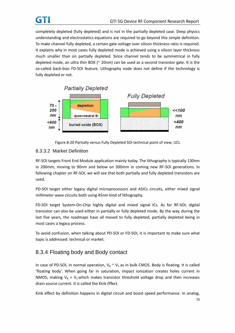
GTI 5G Device RF Component Research Report
70
completely depleted (fully depleted) and is not in the partially depleted case. Deep physics
understanding and electrostatics equations are required to go beyond this simple definition.
To make channel fully depleted, a certain gate voltage over silicon thickness ratio is required.
It explains why in most cases fully depleted mode is achieved using a silicon layer thickness
much smaller than on partially depleted. Since channel tends to be symmetrical in fully
depleted mode, an ultra thin BOX (~ 20nm) can be used as a second transistor gate. It is the
so-called back-bias FD-SOI feature. Lithography node does not define if the technology is
fully depleted or not.
Figure 8-20 Partially versus Fully Depleted SOI technical point of view, UCL
8.3.3.2 Market Definition
RF-SOI targets Front End Module application mainly today. The lithography is typically 130nm
in 200mm, moving to 90nm and below on 300mm in coming new RF-SOI generations. In
following chapter on RF-SOI, we will see that both partially and fully depleted transistors are
used.
PD-SOI target either legacy digital microprocessors and ASICs circuits, either mixed signal
millimeter wave circuits both using 45nm kind of lithography.
FD-SOI target System-On-Chip highly digital and mixed signal ICs. As for RF-SOI, digital
transistor can also be used either in partially or fully depleted mode. By the way, during the
last five years, the roadmaps have all moved to fully depleted, partially depleted being in
most cases a legacy process.
To avoid confusion, when talking about PD-SOI or FD-SOI, it is important to make sure what
topic is addressed: technical or market.
8.3.4 Floating body and Body contact
In case of PD-SOI, in normal operation, VB ~ VS as in bulk CMOS. Body is floating. It is called
‘floating body’. When going far in saturation, impact ionization creates holes current in
NMOS, making VB > VS which makes transistor threshold voltage drop and then increases
drain source current. It is called the Kink Effect.
Kink effect by definition happens in digital circuit and boost speed performance. In analog,

GTI 5G Device RF Component Research Report
71
this non linear effect is often non desirable and designer will design under VDS < ~ 0.6V
(Figure 8-21).
Figure 8-21 Kink effect, UCL
An alternative is to contact the body to keep its voltage constant. It is called ‘body contact’.
In certain case like on RF-SOI antenna switch, body is put under ground, typically 2.5V, to
further reverse the junction capacitance and then reducing their value and non linearity
effect. In case of FD-SOI, there is no Kink Effect (Figure 8-22). Body contact can be still used
to improve linearity for example in case of RF-SOI antenna switch.
Figure 8-22 Kink effect bulk, PD-SOI and FD-SOI, UCL
8.4 CMOS on SOI for RF
Purpose of this chapter is to review the SOI technologies and value for RF, from 4G Front End
Modules to 5G, transceivers and beyond.
8.4.1 RF-SOI
RF-SOI targets Front End Module application building blocks: switch, tuner, power amplifiers,
low noise amplifiers, passives. Simple definition of RF-SOI could be silicon CMOS compatible
layer on quasi lossless substrate.
Performances can be limited by design, back-end of line process (also named metallization),

GTI 5G Device RF Component Research Report
72
Front-End of line (also name diffusion) and substrate (Figure 8-23). RF-SOI substrate target is
to not be a limiting RF performance factor, ideally be a quasi lossless substrate with a high
thermal conductivity enabling lower application cost and smaller footprint.
Figure 8-23 RF-SOI process cross section, UCL
RF-SOI has already 25 years of history (Figure 8-24). HR-SOI and Trap Rich RFeSI™ are the key
inventions that make this technology mainstream for switch and tuner with 90% market
share according to market analyst Navian.
Figure 8-24 History of RF SOI, Soitec
8.4.1.1 HRSOI
HR-SOI (Figure 8-25) is made with Smart Cut™ on high resistive handle substrate (> 1kΩ.cm).

GTI 5G Device RF Component Research Report
73
Figure 8-25 HR-SOI process, Soitec
Despite using high handle substrate resistivity before SmartCut™, the HR-SOI effective
resistivity under AC signal falls down to around 100Ω.cm. BOX is done with silicon oxide.
Although an insulator, this oxide is positively charged. In response to these charges, a
‘parasitic surface conduction’ (PSC) layer is formed under the BOX. This conductive layer
(Figure 8-26) highly degrades the expected RF performances (insertion loss, linearity,
isolation) but still remains better than bulk.
Figure 8-26 Parasitic conductive layer on HR-SOI process, Soitec
8.4.1.2 Trap Rich SOI - RFeSI™
To avoid this parasitic surface conduction, two techniques were invented:
1) HSP (Harmonic Suppression Process) developed by IBM (now Global Foundries) using
lithography.
First, the process etches vias through the BOX, then implants heavy ion to damage the silicon
surface below the BOX and refills the via with oxide. The damaged silicon area has traps that
significantly reduce charge mobility. Beside is also added a contact (poly contact) to bias the
region around the heavy ion implant to further reduce the parasitic surface conduction effect.
This technique cannot be used under transistors. Transistor process needs to be done before
since a high temperature process would cure the damage done by the implant. This
technology requires a thick BOX (>1um).

GTI 5G Device RF Component Research Report
74
Figure 8-27 Cross section of HSP process, IBM (now Global Foundries)
2) Trap Rich layer developed by Soitec and UCL.
This layer is done before the Smart Cut™ bonding process. The trap rich layer is spread across
the entire wafer whereas it is only under passives with HSP techniques. Charge mobility
under the BOX is highly reduced by this high density traps layer. BOX as thin as 200nm can be
used without impacting performances. It enables easier wafer process at both engineering
substrate and foundry side, improving throughput, yield and cost of the manufactured
devices. Soitec branded this technology RFeSI™ (RF enhanced Signal Integrity).
Figure 8-28 Parasitic conductive layer on HR-SOI process, Soitec
Both technologies moved initially in volume production. Most foundries latest generation
processes are now using RFeSI™.
RFeSI™ improves all critical parameters required for RF Front End Module devices. Effective
resistivity of the last generation RFeSI™ is above 8kΩ.cm and measured performances are
getting close to an insulator such as quartz. Further improvements are still expected on
linearity and insertion loss in order to meet the most stringent cases supporting dual
transmission either for carrier aggregation or dual 4G and 5G connectivity cases. Although

GTI 5G Device RF Component Research Report
75
performance limitation may mainly comes from transistors.
Figure 8-29 Electrical characteristics on HR-SOI, Trap Rich SOI and Quartz substrates, UCL
In term of RF-SOI roadmap, the trend is to move to fully depleted to improve switch
Ron*Coff figure of merit. Fully depleted transistors have less stray capacitance thanks to
thinner film. Ron*Coff has been reduced from over 350fs to around 100fs and more
reduction are expected while keeping breakdown voltage constant.
Figure 8-30 Ron*Coff trend versus substrate type, Skyworks
8.4.1.3 RF-SOI for Switch, Tuner, LNA, PA
1) RF-SOI for Switch and Tuner
From an RF-SOI substrate perspective, 90% of switch and tuners are built on RF-SOI as

GTI 5G Device RF Component Research Report
76
illustrated on Figure 8-31.
Figure 8-31 Main RF Front-End modules market, Navian Report 2016
RF-SOI has all key merits to remain the mainstream technology for switch. It is by far the best
tradeoff between performance (meet LTE A PRO specifications), price (Bulk only is cheaper),
area (more and more analog integration (LNA, Tuner, passives …) with digital (MIPI bus,
control logic …)). MEMs have been perceived for years as a potential player for high end
devices. Due to its high cost, low reliability, it remains a challenger.
2) RF-SOI for LNA
For most advanced carrier aggregation case and MIMO, LNA is becoming a key function.
RF-SOI presents three key advantages.
Inductor high quality factor (see next on PA)
Access to 300mm and lithography equal or below 90nm
Integration with switch
Most recent data show that LNAs on RF-SOI are equivalent to SiGe which cannot compete in
integration as it enables poor switch performance.

GTI 5G Device RF Component Research Report
77
Figure 8-32 LNA + SWITCH in advanced FEM architectures, Soitec
Power Amplifier remains the last devices in the RF Front End Module to broadly adopt
RF-SOI.
3) RF-SOI for PA
Power Amplifiers on RF-SOI have major advantages versus bulk:
Inductors quality factor improvement on RFeSI™
M
O
D
E
M
+
T
RA
N
S
C
EI
V
E
R
AntennaSwich Module
FilterBank
(BPF, Dx, Mx)
PA Modeswitch
PowerLow Noise Amplifier
Tx/RxMid
Band
MIPI
Supply Modulator
3GLTE
2G
Tx/RxLowBand
Tx/RxHighBand
Diplexer
Diplexer
MIMO 4x4
1 Tx / 4 Rx
Supply Modulator
3GLTE
2G
Supply Modulator
3GLTE
Rx Diversity switchmodule (x3)
Rx diversityReceive module (x3)
M
O
D
E
M
+
T
RA
N
S
C
EI
V
E
R

GTI 5G Device RF Component Research Report
78
Figure 8-33 Inductor quality factor HR-SOI versus Trap Rich SOI, UCL
Transistor stacking enabling voltage handling beyond single transistor breakdown
voltage
Figure 8-34 Stacked MOSFET Power Amplifier, UCSD
Specific extended drain devices developed by foundries with high BV * Fmax
product

GTI 5G Device RF Component Research Report
79
Figure 8-35 RF power NLDMOS on SOI, STM
Figure 8-36 Electrical characteristics on SOI, STM
RF-SOI AP is adapted and its embedded digital CMOS can be used for tuning at specific band.
Owing to the power density and mobility, the PAE performance of GaAs is so well has to the
main material used for 4G components. While RF-SOI is mainly used towards middle and
low-end smartphone market. In order to expanding the application of RF-SOI for PA, the
foundries and fabless semiconductor companies take great efforts in developing RF-SOI.
As shown in follow figure, RF-SOI is an unique platform which can be fully integrated, and it
is a alternative choice when needed.

GTI 5G Device RF Component Research Report
80
(Figure 8-37, Soitec)
8.4.1.4 RF-SOI eco-system
A technology needs a strong eco-system to become mainstream. All leading foundries have
strong roadmaps to further develop RF-SOI, in both 200mm and 300mm. According to Soitec
estimates, worldwide RF-SOI production in 2017 was 1.3 million wafers 200mm equivalent
moving to 2 millions in 2020.
M
O
D
E
M
+
T
RA
N
S
C
EI
V
E
R
AntennaSwich Module
FilterBank
(BPF, Dx, Mx)
PA Modeswitch
PowerLow Noise Amplifier
Tx/RxMid
Band
MIPI
Supply Modulator
3GLTE
2G
Tx/RxLowBand
Tx/RxHighBand
Diplexer
Diplexer
MIMO 4x4
1 Tx / 4 Rx
Supply Modulator
3GLTE
2G
Supply Modulator
3GLTE
Rx Diversity switchmodule (x3)
Rx diversityReceive module (x3)
M
O
D
E
M
+
T
RA
N
S
C
EI
V
E
R

GTI 5G Device RF Component Research Report
81
Figure 8-38 RF-SOI industry ecosystem, Soitec
8.4.2 PD-SOI for RF
When talking about PD-SOI for RF, target market is mainly related to microwave to mm wave
circuits. As mentioned in the introduction, SOI was mainly used for digital applications like
AMD microprocessor, game console, ASICs till around 2010. Those applications did follow
Moore’s low down to 45nm. IBM now Global Foundries has developed a complete new RF
back end and analog options to adress mmW applications like Low Earth Orbite transceivers,
5G, Automotive radar, etc… A specific SOI substrate was designed re-using same options
used in RF-SOI: high resistivity substrate and trap rich layer.
This technology offers un-matched performance with NMOS Ft/Fmax > 300GHz and PMOS
Ft/Fmax > 250GHz (Figure 8-39).
…
> 10 foundries
in HVM mode
mmW
DAC
ADC
PLL Mixers
+
RFSOI
0.25um
RFSOI
0.18um
RFSOI
0.13um
RFSOI
90nm
RFSOI
65nm
RFSOI
45nm
Addressing current needs
and new challenges
< 6Ghz
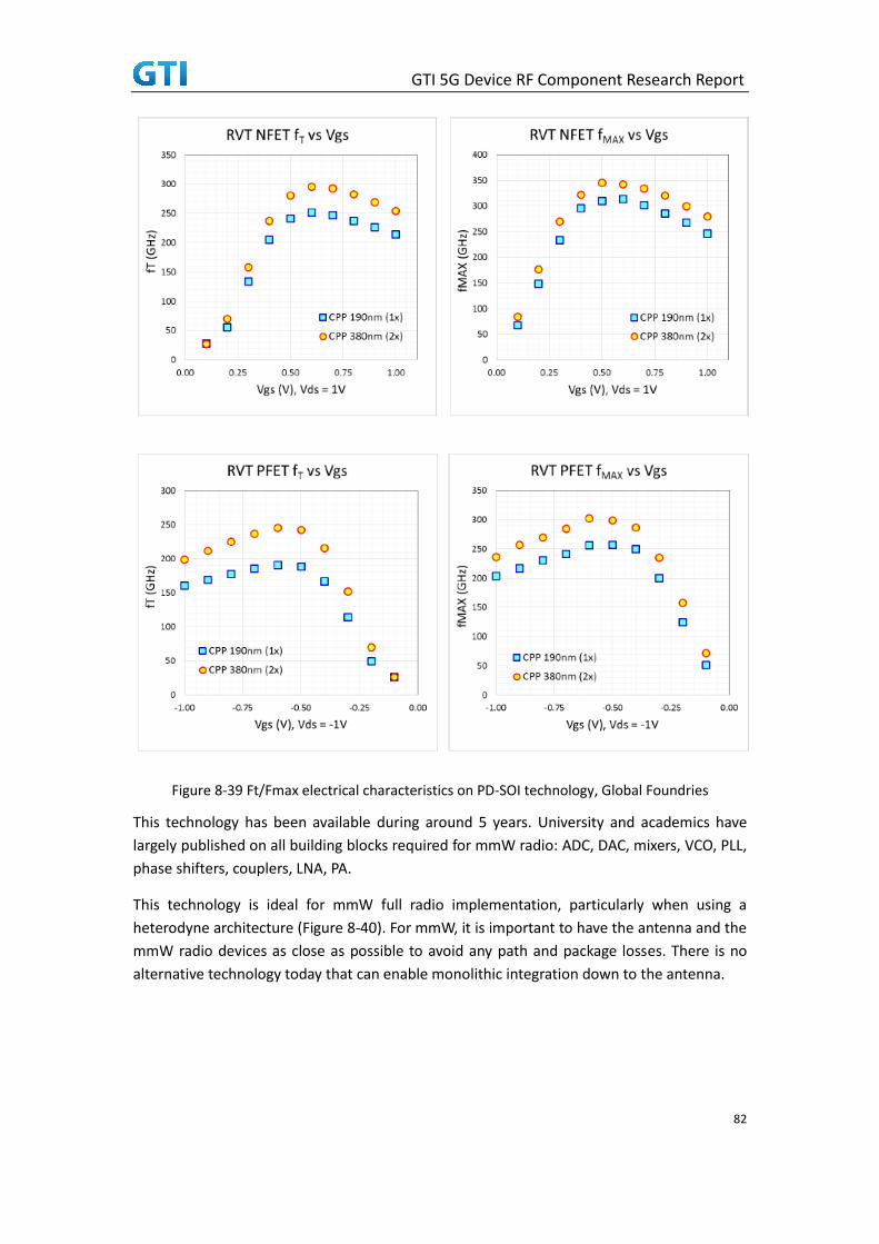
GTI 5G Device RF Component Research Report
82
Figure 8-39 Ft/Fmax electrical characteristics on PD-SOI technology, Global Foundries
This technology has been available during around 5 years. University and academics have
largely published on all building blocks required for mmW radio: ADC, DAC, mixers, VCO, PLL,
phase shifters, couplers, LNA, PA.
This technology is ideal for mmW full radio implementation, particularly when using a
heterodyne architecture (Figure 8-40). For mmW, it is important to have the antenna and the
mmW radio devices as close as possible to avoid any path and package losses. There is no
alternative technology today that can enable monolithic integration down to the antenna.

GTI 5G Device RF Component Research Report
83
Figure 8-40 45nm RF-SOI for 5G mmW Front-End Module, Global Foundries
Skyworks demonstrates 45nm RF-SOI capability for mmW radio devices as illustrated on
Figure 8-41 below.
Figure 8-41 45nm RF-SOI mmW Power Amplifier design (not optimized design, trade off linearity
/ PAE), Skyworks
PD-SOI eco-system is not yet as developed as RF-SOI. ST Microelectronics has a PD-SOI
offering for mmW devices using 65nm lithography as well.
8.4.3 FD-SOI
8.4.3.1 FD-SOI wafer capability
For 28nm lithography and beyond, the FD-SOI technology that has been developed is called
UTBB, standing for Ultra Thin Body and Box. Body stand for the silicon layer typically around
10nm. Box is around 20nm.

GTI 5G Device RF Component Research Report
84
Figure 8-42 UTBB-FD-SOI technology, Soitec and STM
In fully depleted mode, transistor threshold voltage is dependent of the silicon layer
thickness. During many years, the eco-system didn’t engage into this technology fearing that
meeting silicon uniformity specification would not be feasible as Moore’s Law continues.
Volume production having uniformity capability of +/-5Å wafer to wafer has been realized, all
wafer (Figure 8-43). This uniformity is equivalent to few atoms of silicon. Research laboratory
CEA-LETI did demonstrate FD-SOI transistors at 7nm lithography.
Figure 8-43 FD-SOI Silicon thickness uniformity, Soitec
8.4.3.2 Back-Bias
FD-SOI UTBB wafers are designed with ultra thin Box to enable back-bias. Box is used as a
second transistor gate. It enables Vt modulation. Such a technique is also use in Bulk CMOS
but Vt tuning capability is 10 times lower (Figure 8-44).

GTI 5G Device RF Component Research Report
85
Figure 8-44 Forward and reverse back-bias in FD-SOI
In digital applications, transistor can be put in ultra low leakage current mode when idle or in
high performance mode when maximum operating frequency is required (Figure 8-45).
Figure 8-45 Frequency/power flexibility 22nm FD-SOI, Global Foundries
Back-bias is also used to compensate process variation improving circuit yield, performance
spread, minimum operating voltage, etc..., as presented below.

GTI 5G Device RF Component Research Report
86
Figure 8-46 Design compensation with FD-SOI, Soitec
As an example, see trimming results on a 60mm2 28nm processor circuit today in volume
production.
Figure 8-47 Trend Leakage/Operating frequency with FD-SOI, Soitec
In analog, back-bias technique opens the door to new circuit topology since two gates with
two different transconductances are available.
8.4.3.3 FD-SOI for analog
As mentioned in the previous chapter, we can take advantages of FD-SOI material with
back-bias control. Meanwhile, FD-SOI can be used and valuable compared to bulk only with
native devices (no back bias technique). The active device benefits for analog applications
are the following:
Mismatch reduction due to undoped channel and no halo implants compared to
bulk (>30%)

GTI 5G Device RF Component Research Report
87
Figure 8-48 Vth and Idsat mismatch 22nm FD-SOI versus bulk, GlobalFoundries
Higher intrinsic voltage gain than bulk gm/gds (Figure 8-49)
Higher gms/Ids (Figure 8-49)
Lower gds ( as much as 1.8X on bias) than bulk
Lower parasitic capacitance
Figure 8-49 MOSFET DC gain FD-SOI versus bulk, STM
Meanwhile, the use of back bias technic allows PPA (Performance Power Area) advantages:
FBB (Forward Back Gate bias)
Lower vth, increase gm
Increase performances for a given area
Reduce area
FBB (Forward Back Gate bias) less commonly used
Useful for low speed and low power designs to reduce leakage, bias currents
and standby currents
Issues for back bias to address analog design are illustrated with Figure 8-50 and Figure 8-51.

GTI 5G Device RF Component Research Report
88
Moreover back bias techniques should allow performances trimming: Gain, Bandwidth,
Delay …
Figure 8-50 Amplifier bandwidth improvement in 22nm FD-SOI, Global Foundries
Figure 8-51 Analog circuits benefits with back bias in FD-SOI, Global Foundries
For lithography below 22nm, the CMOS roadmap has moved to FinFET. FinFET is a 3D CMOS
structure using thin (Figure 8-52). Gate is around a fin, allowing better electrostatic control
whereas it wasn’t possible anymore on planar CMOS.

GTI 5G Device RF Component Research Report
89
Figure 8-52 FinFET architecture
When comparing FD-SOI UTBB against FinFET without strain, the transistor gain remains
larger, even more when going to narrow channel. Due to lithography constraint, the fin
height and width are fixed which means that designers are losing significant flexibility for
design.
Figure 8-53 Gain MOSFET transistor FD-SOI versus FinFET, SSE 2012
More important, FinFET process is significantly more complex and expensive than SOI CMOS
and also requires more design resources.
8.4.3.4 FD-SOI for System-On-Chip Wireless IC
Based on performance and cost data presented, FD-SOI is the ideal platform for highly
integrated mixed signal system like transceivers integrated with Modem and MCU.
As an example, Sony has launched on the market a fully integrated GPS circuit (receiver +
demodulator + signal processing) claiming that it consumes 5 times less current than the
competition. This circuit is used in Xiaomi SmartWatch and other Tier #1 brand wearable.

GTI 5G Device RF Component Research Report
90
Figure 8-54 Sony GPS circuit in FD-SOI, Global Foundries
8.4.3.5 FD-SOI for mmW
FD-SOI is the logical roadmap following planar CMOS bulk for mmW. FinFET cannot be
effectively used for mmW due to its 3D structure and then large stray capacitance. Ft/Fmax
of FinFet is around half of FD-SOI at same node.
Figure 8-55 MOSFET Cutoff frequency FinFET versus planarFET
Whereas FD-SOI is primary targetting advanced digital signal processing with transceivers, it
keeps intrinsic capabilities of SOI for power amplifiers and switch with reduced output power
capability compared to PD-SOI 45nm (< 20dBm). In case of complex phase array where single
power amplifier output power remains below 20dBm, FD-SOI allows a full 5G system
integration from antenna to digital baseband and application processor using direct
conversion architecture (Figure 8-56).

GTI 5G Device RF Component Research Report
91
Figure 8-56 FD-SOI for 5G mmW Front-End Module, Global Foundries
Using back-bias, some novel architecture can be designed. As an example, the use of
back-bias allows to revisit classical PA architecture (Figure 8-57). The contribution of wide
range FBB bias drives to have a gradually change the overall class of Power Amplifier. In the
same time, optimize efficiency and linearity was optimized.
Figure 8-57 mmW Power Amplifier using back bias in FD-SOI
As of today, FD-SOI has no high resistive bulk options.
8.4.3.6 FD-SOI eco-system
A technology needs a strong eco-system to become mainstream. In early 2010s, ST
Microelectronics and ST-Ericsson were the first to develop and ship cellular microprocessors
on FD-SOI at 28nm. On dual cortex A9 running at 1.85GHz, they demonstrated FD-SOI 28nm
was outperforming versus 28nm Bulk (Figure 8-).

GTI 5G Device RF Component Research Report
92
Figure 8-58 cellular microprocessors power saving FD-SOI versus bulk, STM
In 2017, FD-SOI eco-system is in place with process offering from 65nm down to 12nm from
four different foundries as well as IP and design services. Global Foundries has decided in
2017 to open a new 300mm foundry dedicated to FD-SOI in Chengdu as well as a global IP
design center (Figure 8-59).

GTI 5G Device RF Component Research Report
93
Figure 8-59 FD-SOI ecosystem, Soitec
8.5 Non Silicon Engineered Substrate
8.5.1 Non Silicon materials for RF
Silicon (bulk and SOI) is today mainstream in semiconductors industry with 98% of volume. It
doesn’t mean that non silicon materials are not of interest. As presented in this chapter
introduction, when state of the art performances are required like in Front End Module,
silicon is not dominant anymore.
Ideal characteristics of RF materials are:
Loss less: high resistivity, low permittivity
High resistivity means above 10kΩ.cm: it is at the limit of silicon capability. Low
permittivity means by definition below silicon (Ɛr < 11.3). As an example, glass and
ceramic are ideal. They are used for high end passive device, printed board circuit.

GTI 5G Device RF Component Research Report
94
Figure 8-60 Sate of the Art materials electrical resistivity and thermal conductivity, Soitec
High frequency capable: high electron and hole mobility
High mobility means above 3000 cm2 V-1 s-1 for electron. Compound semiconductors
are ideal, especially because mobility is not so much degraded under high current
density. It makes GaAs an ideal substrate for cellular power amplifiers.
Figure 8-61 Sate of the Art materials’ mobility, UCL
High power and high voltage: high bandgap voltage and thermal resistance
Silicon has 1.22V bandgap voltage. High bandgap material has >3V. For example: GaN,

GTI 5G Device RF Component Research Report
95
Silicon Carbine, Aluminum nitride, Diamond.
Silicon has thermal resistance of 148 W.m-1.K-1. Silicon Carbide and Diamond are much
higher. Heat dissipation can be improved with proper packaging. For example, GaN has not
state of the art properties whereas it is reference material for power.
Figure 8-62 Sate of the Art materials’ bandgap
In theory, there would be an infinite number of offers for engineered substrate materials to
address dedicated RF applications. In practice, a strong eco-system is required in order to
move new material into high volume production. Most of the time, integrated device
manufacturers (IDM) are addressing those markets by developing their own IP and expertise
on substrate, process and circuit design. As an example, Wolfspeed with CREE has developed
a fully integrated supply chain from silicon carbide wafering to gallium nitride circuits (GaN
on SiC) product lines. Part of the GaN market is then captive. GaN on Silicon is an alternative
solution that has been developed. Most of GaN on silicon players are also developing
proprietary process from wafers to end products. It limits then the development of pure play
foundries offering and global eco-system serving high volume at competing cost. Except for
Gallium Arsenide (GaAs), there is no real global eco-system on any other non silicon
engineering substrate materials. As a result, GaAs ecosystem has pure foundries like Win
Semiconductors, AWSC, new entrant like HiWafer and Sanan serving or on top of incumbent
leaders like Skyworks, Qorvo, Broadcom.
This chapter of non silicon material for RF could be pretty exhaustive but since information
are proprietary or addressing niche markets, we just present two examples in following
sub-chapters.

GTI 5G Device RF Component Research Report
96
8.5.2 Example 1: Indium Phosphide on Gallium Arsenide
In 5G mmW front end module roadmap, Indium Phosphide (InP) is often presented as the
best material for power amplifier. As for 4G and 5G sub 6GHz front end module, it is
interesting to note that standard silicon CMOS bulk is not seen as a process of choice (Figure
8-6).
The reason InP is the best material for 5G mmW power amplifier is that it has best Fmax*
Breakdown voltage product figure of merit (FoM)(Figure 8-63). As presented in below figures,
InP FoM outperforms GaAs and SiGe by 10x. State of the art one watt power amplifiers are
today produced using InP bulk material (Figure 8-64).
Figure 8-63 InP FoM, Skyworks
Figure 8-64 Power of PAs state of the arts
InP remains today dedicated to professional market. Main reason is that InP material supply
doesn’t really exists. It is mainly available in 100mm size at extremely high price compared to

GTI 5G Device RF Component Research Report
97
150mm GaAs wafer. For InP to become mainstream in 5G base station and handset, it is then
a must to have it available at competing price and in 150mm size. Using Smart Cut™, a new
structure has been proposed: InP On GaAs (InPOGaAs). This structure removes all roadblocks
of current InP to become mainstream. Affordable cost by re-using multiple time InP
expensive bulk wafer, allows high volume manufacturing but also have low brittleness
equivalent to GaAs and no InP waste. InPOGaAs wafers are fully compatible with GaAs
epitaxy and process lines.
Figure 8-65 Why InP on GaAs, Soitec
InPOGaAs wafers prototypes were built and an epitaxy was performed. It shows excellent
first time right DC transistors characteristics. A strong engagement of key players is now
required to move InPOGaAs as a mainstream process.
Figure 8-66 Soitec wafer prototypes InP On GaAs
8.5.3 Example 2: Piezo on Insulator
In handset front end module, filters content is dominating (Figure 8-67).

GTI 5G Device RF Component Research Report
98
Figure 8-67 RF Front-End modules market, Yole
Filters are done with piezoelectric materials. Piezo materials allow exchange of electrical
energy into mechanical energy and vis-versa. Filter market is the biggest in the MEMs market
segment. There are two kinds of filter structures. Surface acoustic wave (SAW) filters and
bulk acoustic wave (BAW) filters. In SAW, acoustic wave propagates on the surface of the
material. Filter frequency is defined by the interdigital transducers (IDT) made with simple
metal deposition. In BAW filters, acoustic wave propagate in the volume of the material. It is
made of a piezoelectric material layer inserted between two metal layers. BAW structure is
either above a cavity (FBAR – invented by Avago/Broadcom), or above a Bragg mirror (Figure
8-68).

GTI 5G Device RF Component Research Report
99
Figure 8-68 SAW versus BAW Technology comparison, Triquint (now Qorvo)
SAW filters address low – mid band and BAW addresses mid-high band frequencies (Figure
8-69). The temperature stability specifications of the filters are stringent in full duplex mode
especially when guard band between Rx and Tx is limited or when other band are close by. If
the specification of the temperature drift is below 20ppm/oC, the filters are said
‘temperature compensated’. In extreme case, the requirement is to have a ‘zero drift’
frequency over the temperature range.
Figure 8-69 Type of filters versus Area Newtork bands, Qorvo
Piezo On Insulator (POI) defines a piezoelectric material on an insulator (Figure 8-70). For
more than twenty years, theory has showed that new acoustic filters can be made using thin
piezoelectric layers. Murata has announced and published in 2016 a new filter technology
IHP standing for ‘Incredible High Performance’. Murata claims that those filters are
competing with BAW filters. The detail material stack used is not public.
Figure 8-70 POI substrate, Soitec
Using Smart Cut™ and Smart Stacking™ technologies, complex engineered substrates for
filters can be designed.
Mono-crystal Piezolayer
Buried Oxide
High Resistive Base
LTO/Si Smart Cut™ Substrate