growth of high-density carbon nanotube forests on conductive tisin
TRANSCRIPT
Growth of high-density carbon nanotube forests on conductive TiSiN supports
Junwei Yang1, Santiago Esconjauregui
*1, Alex W. Robertson
2, Yuzheng Guo
1, Toby Hallam
3,
Hisashi Sugime1, Guofang Zhong
1, Georg S. Duesberg
3,4, John Robertson
1
1 Department of Engineering, University of Cambridge, CB3 0FA, Cambridge, UK
2 Department of Materials, University of Oxford, Parks Road, OX1 3PH, Oxford, UK
3 Centre for Research on Adaptive Nanostructures and Nanodevices, Trinity College Dublin,
Dublin 2, Ireland
4 School of Chemistry, Trinity College Dublin, Dublin 2, Ireland
We grow vertically-aligned carbon nanotube forests on refractory conductive films of TiSiN
and achieve area densities of (5.1 ± 0.1) × 1012
tubes cm-2
and mass densities of about 0.3 g
cm-3
. The TiSiN films act as diffusion barriers limiting catalyst diffusion into the bulk of the
support, and their low surface energy favours catalyst de-wetting, inducing forests to grow by
the root growth mechanism. The nanotube area density is maximised by an additional
discontinuous AlOx layer which inhibits catalyst nanoparticle sintering by lateral surface
diffusion. The forests and the TiSiN support show ohmic conduction. These results suggest
that TiSiN is the favoured substrate for nanotube forest growth on conductors and liable of
find real applications in microelectronics.
High-density carbon nanotube (CNT) forests on conductive supports are envisaged as
interconnects in microelectronics and as passive heat exchanger (heat sinks) [1-10 ]
. Such
applications require the nanotubes to be grown vertically aligned, and in direct contact, to
conductive substrates. This is to provide an electrically conductive path through the nanotube
support [5,10]
. Another requirement is to achieve a high area density of the tubes in order to
obtain conductivity values comparable to metals, due to a greater number of charge carrying
tubes per unit area. This has driven a great interest in controlling the synthesis of nanotube
forests on metals, in particular, by chemical vapour deposition (CVD) [ 11 -15 ]
. The most
advanced CNT CVD results for forest growth have been achieved using Fe catalyst deposited
on Al2O3. Both materials interact chemically at the contact interface hence restricting lateral
catalyst mobility and enforcing vertical alignment [16]
. However, the use of Al2O3, or other
insulating films as catalyst support, especially if continuous or thicker than ~3 nm, limits the
overall electrical performance of nanotube forest and support [17]
, and ultimately unsuitable
for use as interconnects or heat sinks. To overcome this, we demonstrate high-density CNT
forest growth on TiSiN supports. TiSiN is a refractory, amorphous, conducting material, and
an effective diffusion barrier to metals; hence thin TiSiN films are particularly useful as
support layers for the growth of nanotube forests. The barrier properties are correlated to the
high inter-atomic binding energies as well as the absence of grain boundaries typically found
on metals or metal compounds [18-20]
.
The growth of CNT forests on metals is challenging [21-25]
. As metals and metal
compounds are high-surface-energy materials, it is difficult to form and stabilise metal
nanoparticles for nanotube growth. The difficulty stems from the tendency of the metal
catalyst to alloy with the underlying support, and to diffuse into its bulk. In addition, the
processing gases react with the support degrading the electrical properties. A number of
routes to grow CNT forests directly on conductors have been investigated [26-31]
. They include
use of plasma pretreatment prior to CNT CVD [11,26,28]
, use of Co-Mo co-catalyst [29]
,
oxidation of the topmost surface of the support [27]
, usage of metal silicides as catalyst support
[27,30], employing of a sandwich-like metal stack
[31], or enlarging of the grain size of the
support material [27]
. It is thus possible to grow nanotube forests directly on conductors such
as Ti, W, Ta, Cu, TiN, or silicides. Nevertheless, nanotube CVD on these materials still
remains less robust than on Al2O3 or other dielectrics. The process window is narrow and the
growth easily leads to poor or lateral growth, rather than vertically aligned CNT forests [11,27]
.
By employing TiSiN as catalyst support, we eliminate catalyst diffusion through the grain
boundaries of the support, and simultaneously ensure high electrical conductivity between the
tubes and the material underneath. We find that 0.4nm Fe/0.1nm Al deposited on TiSiN
enforces the growth of high area density CNT forests. The discontinuous Al layer oxidises to
AlOx and this inhibits lateral diffusion and sintering of the catalyst, so maximising the
catalyst particle density. At a growth temperature of 600 °C, we achieve area densities of (5.1
± 0.1) × 1012
tubes cm-2
and mass densities 0.36 ± 0.06 g cm-3
. Electrical measurements
between the tubes and the TiSiN support show ohmic behaviour. This suggests that TiSiN is
potentially useful for applications requiring forest growth on conductors.
To achieve these results, we first sputter nominally 50 nm of TiSiN, on native-oxide-
coated Si(100), using a MaTecK GmbH TiSiN target and 6 keV Ar ions. The TiSiN density is
empirically found to be of 1.9 g cm-3
(using a quartz crystal thickness monitor) and the
thickness is confirmed by atomic force microscopy (AFM). Then, we deposit 0.4 nm of high-
purity Fe, followed by 0.1 nm Al (to minimise catalyst surface diffusion and nanoparticle
sintering [7]
) using a DC magnetron sputtering in 3.5 10-3
mbar of Ar at 20 W.
Subsequently, the samples are introduced (air transfer) in a tube furnace and annealed at 500–
800 °C in 1 bar of H2:Ar (500:1000 sccm) for 5 min. Immediately after annealing, we add 10
sccm of C2H2 for a period of 15 minutes. CNT growth is then terminated by purging the
furnace with Ar 5000 sccm, which is maintained until reaching room temperature.
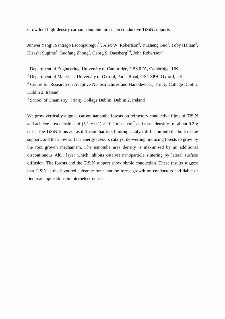
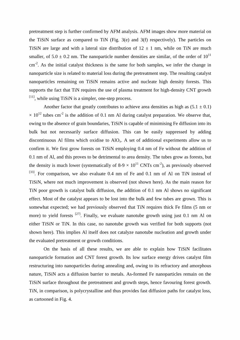
Figure 1 summarises the growth results. Side-view scanning electron microscopy
(SEM) images show well aligned forests which are homogeneous across the samples (Fig.
1(a)). At 600 °C, the average height is 100 ± 5 µm. Closer SEM inspections prove that the
tubes grow in a close-packed array and the forest density appears to be constant along forest
height (insets in Fig. 1(a)). High-resolution transmission electron microscopy (HRTEM)
reveals tubes of 2-3 walls and diameters of 3.0 ± 0.3 nm (Fig. 1(b)). No nanoparticles are
found at the tip of the tubes, suggesting the forests grow by the base growth mechanism. The
mass densities of the forests reach values of 0.31 to 0.42 g cm-3
. By the weight gain method
[32], we assess area densities of (5.1 ± 0.1) × 10
12 tubes cm
-2. Such a value represents the
highest area density of a forest achieved so far on a conducting material, as indicated in Fig.
1(c). AlSi, TiN, or any other metallic supports (e.g. CoSi2) have systematically provided
lower densities, regardless of the pretreatment and growth conditions [26-33]
; only Al2O3 has
yielded greater area density forests [7]
.
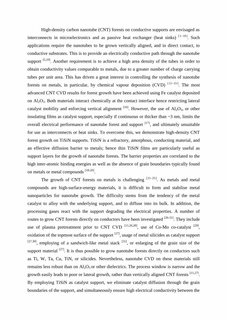
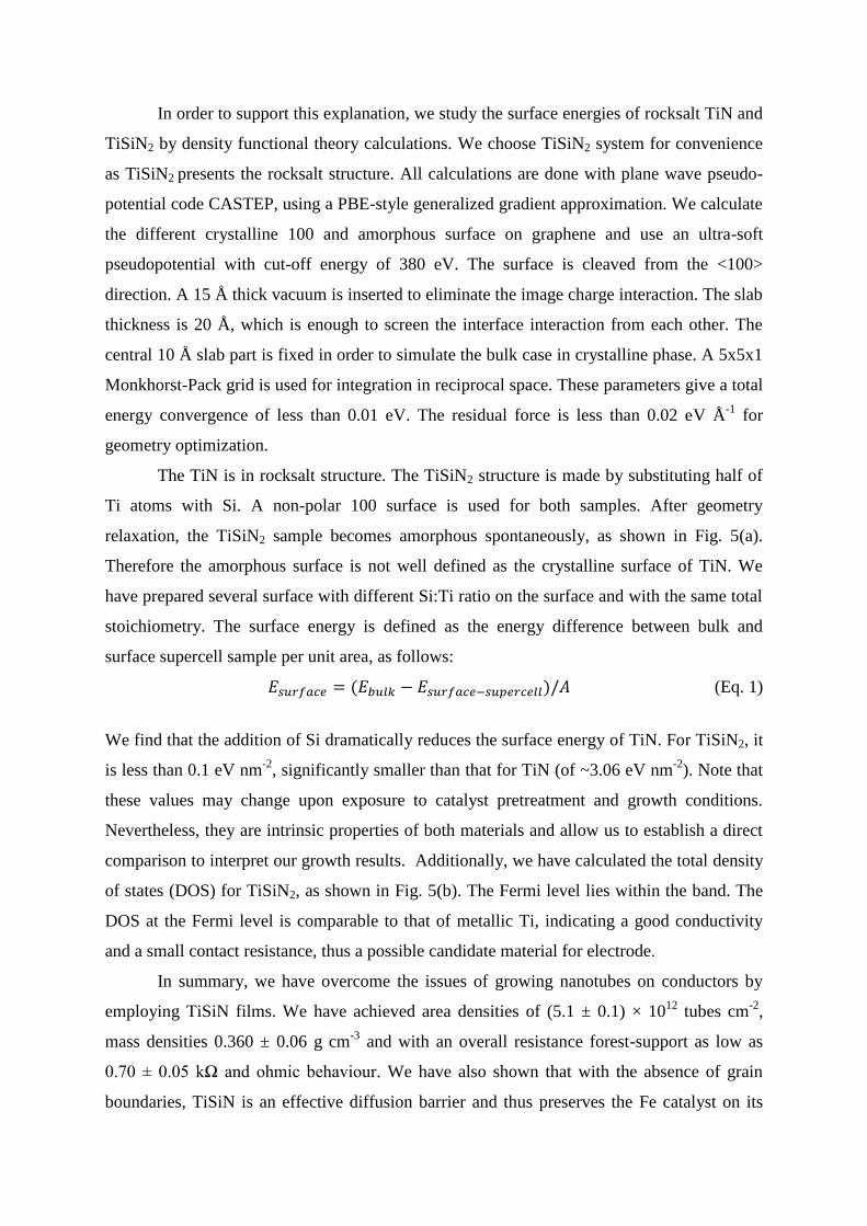
Figure 2 presents further characterisation of the forests and catalyst particles. AFM
analysis shows the forests are seeded by homogeneously-sized Fe nanoparticles (Fig 2 (a)),
with densities as high as (5.8 ± 0.2) 1012
cm-2
. In order to crosscheck the area density values
obtained by the weight gain method, we evaluate the surface coverage by the liquid-induced
compaction method. SEM images show a filling factor [32]
of about ~50 % (Fig. 2(b) and
inset), which is consistent with area densities of the order of 1012
CNTs cm-2
. Finally, by two-
point probe and same set up as previously reported [11]
, we measure the current-voltage
response of the forests, Fig. 2(c). The overall nanotubes-TiSiN support resistance is 0.7 ±
0.05 kΩ and the response is ohmic. This suggests TiSiN is employable as electrode in
nanotube-based microelectronic applications. We comment that nanoparticle formation as
well as nanotube growth results are similar within the whole range of evaluated CVD
conditions.
The area densities of CNT forests on conductors are in general lower than that on
dielectric supports, Fig. 1(c) [27]
. One of the reasons for this is the polycrystalline nature of
the employed materials, which allows catalyst diffusion into the underlying supports. To
overcome this, we need to use conductors that limit catalyst loss, as TiSiN does. It has been
previously demonstrated that TiSiN is an effective diffusion barrier [18-20]
. Because of its lack
of grain boundaries, TiSiN prevents the metal catalysts to diffuse into the underneath support
and allows achieving higher nanotube area densities that on any other conductor. To prove
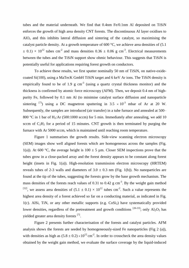
the effect of TiSiN as a diffusion barrier, we compare Fe nanoparticle formation and stability
on TiSiN and TiN. TiN is one of the most studied conductive supports for the synthesis of
forests. For a meaningful comparison, we purposely deposit thicker Fe films (1 nm) on both
supports, perform annealing for 15 min, and compare the amount of Fe on both surfaces by
time-of-flight secondary ion mass spectroscopy (TOF-SIMS), employing the same set up as
previously [34]
(Fig. 3).
We perform depth profiling by TOF-SIMS on 1 nm Fe on TiSiN (a) and (b) on TiN
(c) and (d) before and after annealing. SIMS characterisation (Figs. 3(a) to (d)) confirms that
Fe is preserved on the TiSiN surface, but significantly lost on the TiN. The dashed line shows
the interfaces between Fe and underlying support (Fig. 3(a) to 3(c)). No interface is observed
between Fe and TiN (Fig. 3(d)). This indicates that the Fe layer has diffused into the bulk
TiN. The peak in the secondary ion counts at the interface is caused by oxygen enhancement
effect as a result of the presence of oxygen [35,36]
. This is expected as the samples were
exposed to air after every deposition step. At the start of the measurement, Fe is detected on
the surfaces of the TiSiN and TiN deposited samples, but more pronounced on the surface of
TiSiN (Fig. 3(a) and 3(b)). This suggests that Fe diffusion into TiN may occur before any
annealing, in agreement with previous in-situ photoemission characterisation [11]
. After
annealing, a large peak in the Fe signal shows that Fe is preserved on the surface of TiSiN
(Fig. 3(c)), while the Fe signal decays for the TiN case, Fig. 3(d). Fe diffusion during the
pretreatment step is further confirmed by AFM analysis. AFM images show more material on
the TiSiN surface as compared to TiN (Fig. 3(e) and 3(f) respectively). The particles on
TiSiN are large and with a lateral size distribution of 12 ± 1 nm, while on TiN are much
smaller, of 5.0 ± 0.2 nm. The nanoparticle number densities are similar, of the order of 1011
cm-2
. As the initial catalyst thickness is the same for both samples, we infer the change in
nanoparticle size is related to material loss during the pretreatment step. The resulting catalyst
nanoparticles remaining on TiSiN remains active and nucleate high density forests. This
supports the fact that TiN requires the use of plasma treatment for high-density CNT growth
[11], while using TiSiN is a simpler, one-step process.
Another factor that greatly contributes to achieve area densities as high as (5.1 ± 0.1)
× 1012
tubes cm-2
is the addition of 0.1 nm Al during catalyst preparation. We observe that,
owing to the absence of grain boundaries, TiSiN is capable of minimising Fe diffusion into its
bulk but not necessarily surface diffusion. This can be easily suppressed by adding
discontinuous Al films which oxidise to AlOx. A set of additional experiments allow us to
confirm it. We first grow forests on TiSiN employing 0.4 nm of Fe without the addition of
0.1 nm of Al, and this proves to be detrimental to area density. The tubes grow as forests, but
the density is much lower (systematically of 8-9 × 10¹¹
CNTs cm-2
), as previously observed
[33]. For comparison, we also evaluate 0.4 nm of Fe and 0.1 nm of Al on TiN instead of
TiSiN, where not much improvement is observed (not shown here). As the main reason for
TiN poor growth is catalyst bulk diffusion, the addition of 0.1 nm Al shows no significant
effect. Most of the catalyst appears to be lost into the bulk and few tubes are grown. This is
somewhat expected; we had previously observed that TiN requires thick Fe films (5 nm or
more) to yield forests [27]
. Finally, we evaluate nanotube growth using just 0.1 nm Al on
either TiSiN or TiN. In this case, no nanotube growth was verified for both supports (not
shown here). This implies Al itself does not catalyze nanotube nucleation and growth under
the evaluated pretreatment or growth conditions.
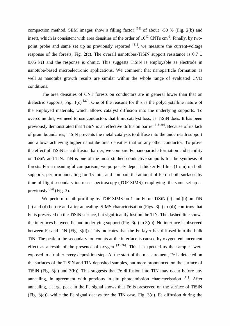
On the basis of all these results, we are able to explain how TiSiN facilitates
nanoparticle formation and CNT forest growth. Its low surface energy drives catalyst film
restructuring into nanoparticles during annealing and, owing to its refractory and amorphous
nature, TiSiN acts a diffusion barrier to metals. As-formed Fe nanoparticles remain on the
TiSiN surface throughout the pretreatment and growth steps, hence favouring forest growth.
TiN, in comparison, is polycrystalline and thus provides fast diffusion paths for catalyst loss,
as cartooned in Fig. 4.
In order to support this explanation, we study the surface energies of rocksalt TiN and
TiSiN2 by density functional theory calculations. We choose TiSiN2 system for convenience
as TiSiN2 presents the rocksalt structure. All calculations are done with plane wave pseudo-
potential code CASTEP, using a PBE-style generalized gradient approximation. We calculate
the different crystalline 100 and amorphous surface on graphene and use an ultra-soft
pseudopotential with cut-off energy of 380 eV. The surface is cleaved from the <100>
direction. A 15 Å thick vacuum is inserted to eliminate the image charge interaction. The slab
thickness is 20 Å, which is enough to screen the interface interaction from each other. The
central 10 Å slab part is fixed in order to simulate the bulk case in crystalline phase. A 5x5x1
Monkhorst-Pack grid is used for integration in reciprocal space. These parameters give a total
energy convergence of less than 0.01 eV. The residual force is less than 0.02 eV Å-1
for
geometry optimization.
The TiN is in rocksalt structure. The TiSiN2 structure is made by substituting half of
Ti atoms with Si. A non-polar 100 surface is used for both samples. After geometry
relaxation, the TiSiN2 sample becomes amorphous spontaneously, as shown in Fig. 5(a).
Therefore the amorphous surface is not well defined as the crystalline surface of TiN. We
have prepared several surface with different Si:Ti ratio on the surface and with the same total
stoichiometry. The surface energy is defined as the energy difference between bulk and
surface supercell sample per unit area, as follows:
(Eq. 1)
We find that the addition of Si dramatically reduces the surface energy of TiN. For TiSiN2, it
is less than 0.1 eV nm-2
, significantly smaller than that for TiN (of ~3.06 eV nm-2
). Note that
these values may change upon exposure to catalyst pretreatment and growth conditions.
Nevertheless, they are intrinsic properties of both materials and allow us to establish a direct
comparison to interpret our growth results. Additionally, we have calculated the total density
of states (DOS) for TiSiN2, as shown in Fig. 5(b). The Fermi level lies within the band. The
DOS at the Fermi level is comparable to that of metallic Ti, indicating a good conductivity
and a small contact resistance, thus a possible candidate material for electrode.
In summary, we have overcome the issues of growing nanotubes on conductors by
employing TiSiN films. We have achieved area densities of (5.1 ± 0.1) × 1012
tubes cm-2
,
mass densities 0.360 ± 0.06 g cm-3
and with an overall resistance forest-support as low as
0.70 ± 0.05 kΩ and ohmic behaviour. We have also shown that with the absence of grain
boundaries, TiSiN is an effective diffusion barrier and thus preserves the Fe catalyst on its

surface during CNT forest growth. These results suggest the feasibility of using TiSiN as
nanotube catalyst support for applications such as interconnects and heat sinks.
Acknowledgement
The authors acknowledge funding from European project Grafol. J.Y. thanks Sarah Fearn and
David McPhail from Imperial College London for use of the SIMS instrument. A.W.R. is
supported by EPSRC (Platform Grants EP/F048009/1 and EP/K032518/1) and Korean
Institute for Energy Research. H.S. acknowledges a research fellowship from the Japanese
Society for the Promotion of Science.
Captions
Figure 1: Growth results on TiN. (a) Side-view SEM image of CNT forest grown using 0.4
nm Fe / 0.1 nm Al at 600 °C. Insets show the forest density is homogenous along forest
height. (b) is a HRTEM of the tubes. (c) Comparison of nanotube area densities of forests
grown on conductors and insulators.
Figure 2: (a) AFM images of the catalyst particles (0.4 nm Fe / 0.1nm Al). Annealing
conditions are 600 °C in 1 bar Ar:H2 (1000:500 sccm) for 5 min. (b) Top-view SEM images
of CNT forest after compaction (inset shows a side-view image). (c) I-V curves obtained on
CNT forests on TiSiN. The behaviour is ohmic.
Figure 3: SIMS depth profile of (a–b) deposited and (c–d) annealed 1 nm Fe at 750 °C in 1
bar Ar:H2 (1000:500 sccm) for 15 min, on TiSiN and TiN respectively. (e–f) are
corresponding AFM images of the particles after annealing.
Figure 4: Schematic model comparing CNT growth between TiSiN and TiN supports.
Figure 5: (a) Atomic structure of TiSiNi2 after relaxation. The initial structure is a perfect
crystal in rocksalt with half Ti substituted by Si. The amorphous state is reached
spontaneously. (b) DOS for amorphous TiSiN2. The Fermi level is labelled by the dashed
line.
Figure 1
25 µm200 nm
5 nm
200 nm
200 nm
(b)
(a)
(c)
Esconjauregui [26]
Zhang [30]
Dijon [21]
current results
close-pack limitdewetting limit
Yokoyama [25]
Zhong [7]
Hata [14]
conductorsinsulators
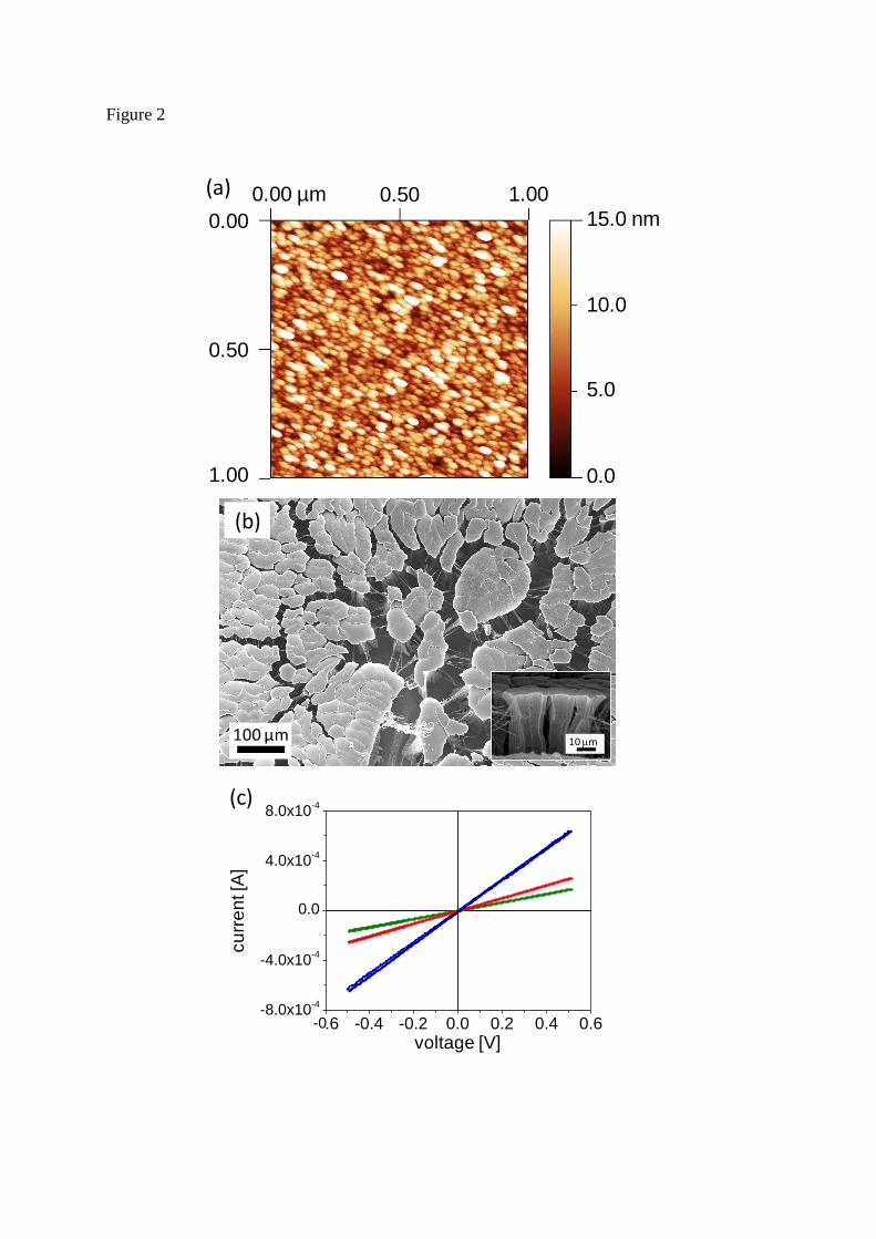
Figure 2
0.00 µm 0.50 1.00
0.0
5.0
10.0
15.0 nm 0.00
0.50
1.00
cu
rre
nt [A
]
voltage [V]-0.6 -0.4 -0.2 0.0 0.2 0.4 0.6
-8.0x10⁻⁶
-4.0x10⁻⁶
0.0
4.0x10⁻⁶
8.0x10⁻⁶
-0.6 -0.4 -0.2 0.0 0.2 0.4 0.6-8.0x10
-4
-4.0x10⁻⁴
0.0
4.0x10⁻⁴
8.0x10⁻⁴(c)
(a)
100 µm
(b)
10 mm
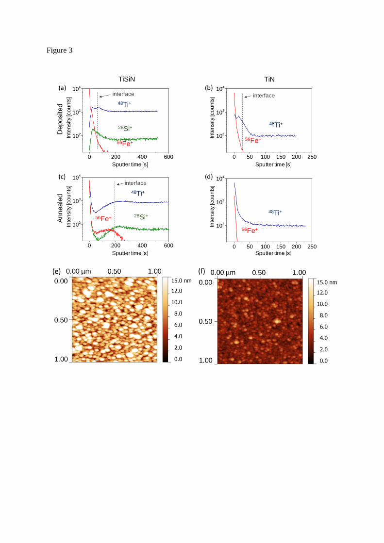
Figure 3
TiSiN TiN
Deposited
Anneale
dIn
ten
sity [c
ou
nts
]
Sputter time [s]
Inte
nsity [c
ou
nts
]
Sputter time [s]
Inte
nsity [c
ou
nts
]
Sputter time [s]
Inte
nsity [c
ou
nts
]
Sputter time [s]
48Ti+
28Si+
56Fe+
48Ti+
28Si+56Fe+
48Ti+
56Fe+
48Ti+
56Fe+
(a) (b)
(c) (d)
interface interface
interface
0 200 400 600
102
103
104
0 200 400 600
102
103
104
0 50 100 150 200 250
102
103
104
0 50 100 150 200 250
102
103
104
0.00 µm 0.50 1.00
0.00
0.50
1.00
0.00 µm 0.50 1.00
0.00
0.50
1.00
(e) (f)
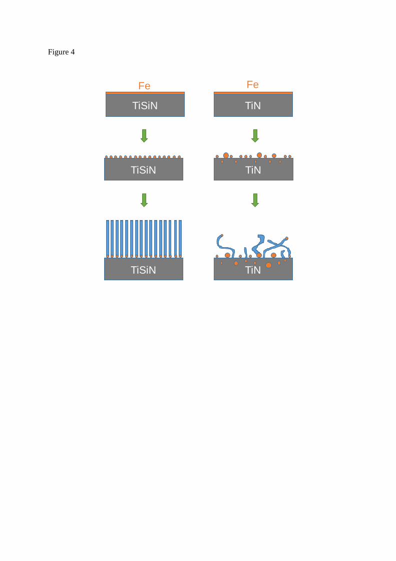
Figure 4
TiNTiSiN
TiSiN
TiSiN
TiN
TiN
Fe Fe
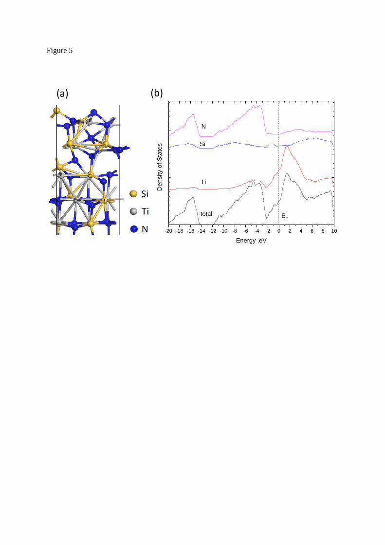
Figure 5
(b)
-20 -18 -16 -14 -12 -10 -8 -6 -4 -2 0 2 4 6 8 10
N
Si
Ti
De
nsity o
f S
tate
s
Energy ,eV
EF
total
(a)
References
1 Y. Awano, S. Sato, M. Nihei, T. Sakai, Y. Ohno, and T. Mizutani, Proc. IEEE 98, 2015
(2010).
2 S. Fan, M. G. Chapline, N. R. Franklin, T. W. Tombler, A. M. Cassell, and H. Dai, Science
283, 512 (1999).
3 D. N. Futaba, K. Hata, T. Yamada, T. Hiraoka, Y. Hayamizu, Y. Kakudate, O. Tanaike, H.
Hatori, M. Yumura, and S. Iijima, Nat. Mater. 5, 987 (2006).
4 D. Acquaviva, A. Arun, S. Esconjauregui, D. Bouvet, J. Robertson, R. Smajda, A. Magrez,
L. Forro, and A.M. Ionescu, Appl. Phys. Lett. 97, 233508 (2010).
5 J. Robertson, G Zhong, S. Esconjauregui, B. C. Bayer, C. Zhang, M. Fouquet, and S.
Hofmann, Jpn. J. Appl. Phys. 51, 01AH01 (2012).
6 Y. Hayamizu, T. Yamada, K. Mizuno, R. C. Davis, D. N. Futaba, M. Yumura, and K. Hata,
Nat Nano 3, 289 (2008).
7 G. Zhong , J. Warner, M. Fouquet, A. Robertson, B. Chen, and J. Robertson, ACS Nano 6,
2893 (2012).
8 S. Sato, K. Hayashi, K. Yagi, D. Kondo, A. Yamada, N. Harada, M. Nihei, and N.
Yokoyama. ECS Transac. 37, 121 (2011).
9 M. Nihei, A. Kawabata, D. Kondo, M. Horibe, S. Sato, and Y. Awano, Jpn. J. Appl. Phys.
44, 1626 (2005).
10 J. Robertson, G. Zhong, S. Hofmann, B. C. Bayer, S. Esconjauregui, H. Telg, and C.
Thomsen, Diam. Relat. Mater. 18, 957 (2009).
11 S. Esconjauregui, B. C. Bayer, M. Fouquet, C. T. Wirth, F. Yan, R. Xie, C. Ducati, C.
Baehtz, C. Castellarin-Cudia, S. Bhardwaj, C. Cepek, S. Hofmann, and J. Robertson, J. Appl.
Phys. 109, 114312 (2011).
12 S. Esconjauregui, M. Fouquet, B. C. Bayer, S. Eslava, S. Khachadorian, S. Hofmann, and
J. Robertson, J. Appl. Phys. 109, 044303 (2011).
13 K. Hasegawa and S. Noda, ACS Nano 5, 975 (2011).
14 K. Hata, D. N. Futaba, K. Mizuno, T. Namai, M. Yumura, and S. Iijima, Science 306,
1362 (2004).
15 S. Sakurai, H. Nishino, D. N. Futaba, S. Yasuda, T. Yamada, A. Maigne, Y. Matsuo, E.
Nakamura, M. Yumura, and K. Hata, J. Am. Chem. Soc. 134, 2148 (2011).
16 C. Mattevi, C. T. Wirth, S. Hofmann, R. Blume, M. Cantoro, C. Ducati, C. Cepek, A.
Knop-Gericke, S. Milne, C. Castellarin-Cudia, S. Dolafi, A. Goldoni, R. Schloegl, and J.
Robertson, J. Phys. Chem. C 112, 12207 (2008).
17 S. Esconjauregui, R. Xie, Y. Guo, S. M.-L. Pfaendler, M. Fouquet, R. Gillen, C. Cepek, C.
Castellarin-Cudia, S. Eslava, and J. Robertson, Appl. Phys. Lett. 102, 113109 (2013).
18 J. S. Reid, E. Kolawa, R. P. Ruiz, and M. A. Nicolet, Thin Solid Films 236, 319 (1993).
19 J. S. Reid, X. Sun, E. Kolawa, and M. A. Nicolet, Electron Devic. Lett., IEEE 15, 298
(1994).
20 J. S. Reid, E. Kolawa, C. M. Garland, M. A. Nicolet, F. Cardone, D. Gupta, and R. P. Ruiz,
J. Appl. Phys. 79, 1109 (1996).
21 J. Dijon, H. Okuna, M. Fayolle, T. Vo, J. Pontcharra, D. Acquaviva, D. Bouvet, A.
Ionescu, S. Esconjauregui, B. Capraro, E. Quesnel, and J. Robertson, Tech Digest IEDM 33,
4 (2010).
22 Y. Wang, B. Li, P. S. Ho, Z. Yao, and L. Shi, Appl. Phys. Lett. 89, 183113 (2006).
23 Y. Wang, Z. Luo, B. Li, P. S. Ho, Z. Yao, L. Shi, E. N. Bryan, and R. J. Nemanich, J.
Appl. Phys. 101, 124310 (2007).
24 A. M. Rao, D. Jacques, R. C. Haddon, W. Zhu, C. Bower, and S. Jin, Appl. Phys. Lett. 76,
3813 (2000).
25 D. Yokoyama, T. Iwasaki, T. Yoshida, H. Kawarada, S. Sato, T. Hyakushima, M. Nihei,
and Y. Awano, Appl. Phys. Lett. 91, 263101 (2007).
26 S. Esconjauregui, B. C. Bayer, M. Fouquet, C. T. Wirth, C. Ducati, S. Hofmann, and J.
Robertson, Appl. Phys. Lett. 95, 173115 (2009).
27 S. Esconjauregui, S. Bhardwaj, J. Yang, C. Castellarin-Cudia, R. Xie, L. D’Arsié, T.
Makaryan, H. Sugime, S. Eslava, C. Cepek, and J. Robertson, Carbon 73, 13 (2014).
28 S. Esconjauregui, C. Cepek, M. Fouquet, B. C. Bayer, A. D. Gamalski, B. Chen, R. Xie, S.
Bhardwaj, C. Ducati, S. Hofmann, and J. Robertson, J. Appl. Phys. 112, 034303 (2012).
29 H. Sugime, S. Esconjauregui, J. Yang, L. Arsié, R. A. Oliver, S. Bhardwaj, C. Cepek, and
J. Robertson, Appl. Phys. Lett. 103, 073116 (2013).
30 C. Zhang, F. Yan, C. S. Allen, B. C. Bayer, S. Hofmann, B. J. Hickey, D. Cott, G. Zhong,
and J. Robertson, J. Appl. Phys. 108, 024311 (2010).
31 G. Zhong, R. Xie, J. Yang, and J. Robertson, Carbon 67, 680 (2014).

32 S. Esconjauregui, R. Xie, M. Fouquet, R. Cartwright, D. Hardeman, J. Yang, and J.
Robertson, J. Appl. Phys, 113, 144309 (2013).
33 J. Yang, S. Esconjauregui, H. Sugime, T. Makaryan, T. Hallam, G. Duesberg, and J.
Robertson, Phys. Sta. Sol. B 251, 2389 (2014).
34 C. Zhang, R. Xie, B. Chen, J. Yang, G. Zhong, and J. Robertson, Carbon 53, 339 (2013).
35 J. C. Lee, H. J. Kang, K. J. Kim, Y. S. Kim, and D. W. Moon, Surf. Sci. 324, 338 (1995).
36 M. L. Yu, Nucl. Instr. Meth. Phys. Res. 15, 151 (1986).