growth and properties of compound …lib.tkk.fi/diss/2006/isbn9512281104/isbn9512281104.pdfgrowth...
TRANSCRIPT

Helsinki University of Technology
Department of Electrical and Communications Engineering
Optoelectronics Laboratory
Espoo, Finland 2006
GROWTH AND PROPERTIES OF COMPOUND
SEMICONDUCTORS ON GERMANIUM SUBSTRATE
Lauri Knuuttila
Helsinki University of Technology
Department of Electrical and Communications Engineering
Optoelectronics Laboratory
Dissertation for the degree of Doctor of Science in Technology to be presented with due
permission of for public
examination and debate in Auditorium TU1 at (Espoo,
Finland) on the 5th of May, 2006, at 12 o´clock noon.
the Department of Electrical and Communications Engineering,
Helsinki University of Technology
Distribution:
Helsinki University of Technology
Department of Electrical and Communications Engineering
Optoelectronics Laboratory
P.O.Box 3500
FIN-02015 HUT
FINLAND
Tel: +358 9 4511
Fax: +358 9 451 3128
© Lauri Knuuttila
ISBN 951-22-8109-0 (printed version)
ISBN 951-22-8110-4 (electronic version)
Picaset Oy
Helsinki 2006

ABHELSINKI UNIVERSITY OF TECHNOLOGY
P. O. BOX 1000, FI-02015 TKK
http://www.tkk.fi
ABSTRACT OF DOCTORAL DISSERTATION
Author Lauri Knuuttila
Name of the dissertation
Date of manuscript January 23, 2006 Date of the dissertation May 5, 2006
Article dissertation (overview + original articles) Number of pages 69 + 55
Department
Laboratory
Field of research
Opponent
Supervisor
Abstract
Keywords
Ge substrate, GaAs, GaInNAs, InAs, quantum well, quantum dot, compound semiconductor
ISBN (printed) 951-22-8109-0
ISBN (pdf) 951-22-8110-4
Publisher Helsinki University of Technology, Optoelectronics Laboratory
The dissertation can be read at http://lib.tkk.fi/Diss/2006/isbn9512281104/
Growth and properties of compound semiconductors on germanium substrate
Department of Electrical and Communications Engineering
Optoelectronics laboratory
Nanotechnology
Prof. Heli Jantunen
Prof. Harri Lipsanen
The aim of this thesis is to investigate the growth and characterisation of compound semiconductors ongermanium (Ge) substrates. Also properties of detector applications and novel Ga(In)NAs compounds arepresented on Ge substrates. The epitaxial growth is performed using metalorganic vapour phase epitaxy(MOVPE) technique.
The nucleation of zinc blende lattice compound semiconductors on the surface of diamond lattice Ge arehighly affected by different growth conditions such as temperature, growth rate and partial pressure of sourcematerials. Thus, thorough characterisation of the fabricated structures and optimisation of the growth pa-rameters are required. Three-dimensional island formation was observed for initial growth phases of GaAsand In(Ga)As on Ge. The properties of the self-assembled islands were investigated using atomic force mi-croscopy (AFM). In0.5Ga0.5As islands grown at low temperature of 550◦C showed a high areal density of3.5 × 1010 cm−2 and uniformity in size. For grown GaAs layers the high initial island density and uni-formity enables homogeneous coalescence of the islands as the growth is continued and results in smoothtwo-dimensional GaAs surfaces already at small layer thicknesses.
The crystal and optical properties of GaAs and Ga(In)NAs layers were investigated using high resolutionX-ray diffraction (HRXRD), synchrotron X-ray topography (SXT) and photoluminescence (PL). In SXTmeasurements a 650 nm thick GaAs layer grown on Ge showed very small dislocation density of 250−500 cm−2.The value is better than was found by SXT for the vapour pressure controlled Czochralski (VCz) grown GaAssubstrates. The growth of GaAs on misoriented Ge substrate results in a tilt angle between the lattice planesof the substrate and the layer. For these structures it was shown that a specific HRXRD setup, in whichthe diffraction plane is parallel with the step edges on the Ge surface, enables accurate measurements andanalyses of the structures.
From a GaInNAs multi-quantum well structure on Ge photoluminescence at telecommunication wavelengthof 1.55 µm was obtained. From the HRXRD and PL results a nitrogen incorporation of about 5 % wasdetermined for the quantum wells. Also for a GaAs/Ge matrix detector structure a record low leakagecurrent of 3× 10⁻⁹ A/cm2 was obtained at 77 K. From arsenic diffusion based matrix detector fabricated onGe substrate an excellent resolution of 220 eV at 5.9 keV and 400 eV at 60 keV was measured.

ABTEKNILLINEN KORKEAKOULU
PL 1000, 02015 TKK
http://www.tkk.fi
VAITOSKIRJAN TIIVISTELMA
Tekija Lauri Knuuttila
Vaitoskirjan nimi
Kasikirjoituksen jattamispaivamaara 23.1.2006 Vaitostilaisuuden ajankohta 5.5.2006
Yhdistelmavaitoskirja (yhteenveto + erillisartikkelit) Sivumaara 69 + 55
Osasto
Laboratorio
Tutkimusala
Vastavaittaja
Tyon valvoja
Tiivistelma
Asiasanat
Ge alustakide, GaInNAs, InAs, kvanttikaivo, kvanttipiste, yhdistepuolijohde
ISBN (painettu) 951-22-8109-0
ISBN (pdf) 951-22-8110-4
Julkaisija Teknillinen korkeakoulu, Optoelektroniikan laboratorio
Luettavissa verkossa osoitteessa http://lib.tkk.fi/Diss/2006/isbn9512281104/
Yhdistepuolijohteiden kasvu germaniumalustakiteelle ja rakenteiden karakterisointi
Sahko- ja tietoliikennetekniikan osasto
Optoelektroniikka
Nanoteknologia
Prof. Heli Jantunen
Prof. Harri Lipsanen
Tyossa kasitellaan yhdistepuolijohteiden kasvua germaniumalustakiteille seka rakenteiden karakterisointia.Tyossa esitetaan myos tuloksia germaniumiin perustuvista rontgendetektoreista ja germaniumille valmis-tetuista tietoliikenneaallonpituuksilla emittoivista GaInNAs-rakenteista. Yhdistepuolijohteet valmistettiinmetallo-orgaanisella kaasufaasiepitaksilaitteistolla (MOVPE).
Kasvuolosuhteet kuten lampotila, kasvunopeus ja lahtoaineiden osapaineet kasvureaktorissa vaikuttavatmerkittavasti sinkkivalkehilaisten yhdistepuolijohteiden nukleaatioon timanttihilaisen germaniumin pin-nalla. Naiden useiden kasvuparametrien optimointi edellyttaa yksityiskohtaista rakenteiden karakterisointia.GaAs- ja In(Ga)As-yhdisteiden kolmiulotteista saarekemuodostumista tutkittiin atomivoimamikroskoopilla.Matalassa 550◦C:een kasvulampotilassa valmistettujen kooltaan hyvin homogeenisten itseorganisoituneidenIn0.5Ga0.5As-saarekkeiden tiheydeksi mitattiin 3.5 × 1010 cm−2. Suuri saareketiheys ja homogeeninen kokomahdollistavat saarekkeiden yhdistymisen pienempina kun kasvatusta edelleen jatketaan. Tama nopeuttaavalmistettavan GaAs kerroksen kasvumoodin muuttumista kaksiulotteiseksi kasvuksi ja tasainen pinta muo-dostuu pienemmilla kerrospaksuuksilla.
Naytteiden kidelaatua ja optisia ominaisuuksia tutkittiin kayttamalla rontgendiffraktometria,rontgentopografia- ja fotoluminesenssimittauksia. Rontgendiffraktiossa vaikeutena ovat Ge-alustakiteenja epitaktisten kerrosten suhteessa toisiinsa kallistuneet hilatasot. Rakenteiden mittaamisen mahdollistaaerityinen mittausgeometria, jossa alustakiteen askelreunat yhtyvat diffraktiotasoon. Rontgentopografialla mi-tattiin germaniumille valmistetusta 650 nm:n paksuisesta GaAs-kerroksesta erittain alhainen 250−500 cm−2
dislokaatiotiheys.
Germaniumille valmistetusta GaInNAs-kvanttikaivokerrosrakenteesta mitattiin emissiota 1,55 µm aal-lonpituudella, joka on yleisesti kaytossa tietoliikennekomponenteissa. Perinteisesti komponentit nainpitkille aallonpituuksille joudutaan valmistamaan InP:iin perustuvista yhdisteista. Rontgendiffraktio- jafotoluminesenssimittauksista GaInNAs-kvanttikaivojen typpipitoisuudeksi maaritettiin 5 %. GaAs/Ge-matriisidetektorirakenteille mitattiin ennatyspieni vuotovirrantiheys 3 × 10⁻⁹ A/cm2 77 K:n lampotilassaja arseenidiffuusiolla valmistetuista Ge-matriisidetektoreista mitattiin erinomainen 220 eV resoluutio 5,9 keVenergialla ja 400 eV resoluutio 60 keV energialla.


Preface
The work presented in this thesis has been carried out in OptoelectronicsLaboratory of Helsinki University of Technology between 2000 and 2006. Iwant to express my gratitude to Professors Turkka Tuomi and Harri Lip-sanen for an opportunity to work in the field of semicondutor epitaxy andfor the support during the time. I am grateful to Docent Markku Sopanenand Dr. Juha Toivonen for introducing MOVPE technique to me and forproviding the guidance especially in the beginning. M.Sc. Marco Mattila Iwould like to thank for setting up the new MOVPE laboratory with me inthe Micronova building and also M.Sc. Outi Reentilä for the collaborationin the epitaxial growth of sometimes mysterious three-five nitrides.
I want to thank Prof. Patrick McNally from the Dublin City University, soonto be Dr. Juha Riikonen, M.Sc. Aapo Lankinen, M.Sc. Antti Säynätjoki andM.Sc. Pasi Kostamo for the cooperation in the various places and occasions.The Graduate school of electronics, telecommunications and automation isacknowledged for their financial support of this work.
I have enjoyed the company of many people working in the OptoelectronicsLaboratory, thanks to you, especially the enthusiasm of Dr. Karri Varisprovided many moments of true inspirations during the time. Thanks tofriends outside the office and to Leo for taking care of outdoor activitiesand clearing the thoughts.
I want to express great gratitude to my parents for the constant supportand encouragement. My two brothers I thank for showing great examplehow this is done. Finally, my greatest gratitude and love to Liisa for alwaysbelieving in me and loving me back.
Espoo, March 2006 Lauri Knuuttila
vii

Table of Contents
Preface . . . . . . . . . . . . . . . . . . . . . . . . . . . . . . . . vii
Table of Contents . . . . . . . . . . . . . . . . . . . . . . . . . . . viii
List of Publications . . . . . . . . . . . . . . . . . . . . . . . . . . x
Author’s contribution . . . . . . . . . . . . . . . . . . . . . . . . xi
1 Introduction 1
1.1 Germanium material . . . . . . . . . . . . . . . . . . . . . . 1
1.2 Germanium heteroepitaxy . . . . . . . . . . . . . . . . . . . 2
1.3 Structure of thesis . . . . . . . . . . . . . . . . . . . . . . . 4
2 Metalorganic vapour phase epitaxy 5
2.1 Growth regimes . . . . . . . . . . . . . . . . . . . . . . . . . 6
2.2 Application of surface kinetics limited growth regime . . . . 7
2.3 MOVPE equipment . . . . . . . . . . . . . . . . . . . . . . . 9
2.4 Comparison of MOVPE and MBE techniques . . . . . . . . 11
3 Interfacial phenomena 12
3.1 Nucleation morphology . . . . . . . . . . . . . . . . . . . . . 12
3.2 Initial growth phases of GaAs . . . . . . . . . . . . . . . . . 16
viii

3.3 Ge surface reconstruction and morphology of GaAs layers . 18
4 Crystal properties and defects 24
4.1 Characterisation of tilted structures by X-ray diffraction . . 24
4.2 Analysing defects using synchrotron X-ray topography . . . 30
4.3 Optical characteristics and interfacial diffusion . . . . . . . 32
5 Applications 34
5.1 Radiation detectors . . . . . . . . . . . . . . . . . . . . . . . 35
5.2 GaAs based nitride compounds on Ge . . . . . . . . . . . . 37
6 Summary 43
References 45
ix

List of Publications
This thesis consists of an overview and of the following publications whichare referred to in the text by their Roman numerals.
I L. Knuuttila, A. Lankinen, J. Likonen, H. Lipsanen, X. Lu, P. Mc-Nally, J. Riikonen, and T. Tuomi, Low Temperature Growth GaAson Ge, Japanese Journal of Applied Physics 44, 7777–7784 (2005).
II L. Knuuttila, K. Kainu, M. Sopanen, and H. Lipsanen, In(Ga)Asquantum dots on Ge substrate, Journal of Materials Science: Mate-rials in Electronics 14, 349–352 (2003).
III L. Knuuttila, T. Korkala, M. Sopanen, and H. Lipsanen, Self-assembled In(Ga)As islands on Ge, Journal of Crystal Growth 272,221–226 (2004).
IV T. Tuomi, L. Knuuttila, J. Riikonen, P. McNally, W. Chen, J.Kanatharana, M. Neubert, and P. Rudolph, Synchrotron X-ray to-pography of undoped VCz GaAs crystals, Journal of Crystal Growth237-239, 350–355 (2002).
V A. Lankinen, L. Knuuttila, T. Tuomi, P. Kostamo, A. Säynätjoki,J. Riikonen, H. Lipsanen, P. McNally, H. Sipilä, S. Vaijärvi, andD. Lumb, Synchrotron X-ray topography study of defects in epitax-ial GaAs on high-quality Ge, accepted for publication in NuclearInstruments and Methods in Physics Research Section A, 4 pages.
VI J. Toivonen, T. Tuomi, J. Riikonen, L. Knuuttila, T. Hakkarainen,M. Sopanen, H. Lipsanen, P. McNally, W. Chen, and D. Lowney,Misfit dislocations in GaAsN/GaAs interface, Journal of MaterialsScience: Materials in Electronics 14, 267–270 (2003).
VII L. Knuuttila, O. Reentilä, M. Mattila, and H. Lipsanen, Compari-son of Ge and GaAs Substrates for Metalorganic Vapor Phase Epi-taxy of GaIn(N)As Quamtum Wells, Japanese Journal of AppliedPhysics 44, L1475–L1477 (2005).
VIII P. Kostamo, A. Säynätjoki, L. Knuuttila, H. Lipsanen, H. Anders-son, K. Banzuzi, S. Nenonen, H. Sipilä, S. Vaijärvi, and D. Lumb,Ge/GaAs heterostructure matrix detector, accepted for publicationin Nuclear Instruments and Methods in Physics Research SectionA, 4 pages.
x

Author’s contribution
The author has written the manuscripts for publications I, II, III, and VII,and he has contributed to the data analysis and manuscripts for publicationsIV, V, VI, and VIII. The author has designed sample structures, growthparameters and completed the growth for the samples in publications I, II,III, V, VII, and VIII where he has especially focused on the growth aspectof compound semiconductors on Ge substrates and on characterisation ofthese structures.
The author has performed the surface morphology studies for the publi-cations I, II, and III, and he has done the optical measurements for thepublications I, II, and VII. The X-ray diffraction studies for the publica-tions I, II, and VII were performed by the author. The synchrotron X-raytopography studies for publication I, IV, and V were mainly carried out bythe author and assisted by the co-authors of publications. For the publica-tion VI the author participated in the fabrication of the samples and in thesynchrotron X-ray topography studies.
xi


1 Introduction
Semiconductors are practically found almost from every electrical device.The continuous research of novel material solutions and development offabrication methods enables new and more advanced devices in our livefrequently. Optical telecommunication technology and optical data stor-age is based on semiconductor lasers and light emitting devices (LEDs) aregradually substituting incandescent lamps in various applications. Theseadvanced components require nearly perfectly controlled epitaxial growthof compound semiconductors. The ability to control the alloying of binarycompounds and the possibility to fabricate coherently strained thin lay-ers with sharp interfaces enables tailoring of the electronic band structure(∼ i.e., ”colour of light”) of compound semiconductors. Semiconductors arealso essential when receiving radiation, that is, in detecting instruments andin solar cells. Using compound semiconductors the performance of these de-vices can be further enhanced.
1.1 Germanium material
The element germanium was discovered by a German chemist C. Winklerin 1886. Prior to that in 1871 the existence of an element later know asgermanium was predicted by D. Mendeleev. Germanium is a group fourelement along with carbon, silicon, tin and lead from which Ge and Si arewidely used as semiconductors. Ge has a diamond lattice that is composedof two interpenetrating face centred cubic (FCC) lattices, one displaced1/4 of a lattice constant in each direction from the other. Each site istetrahedrally coordinated with four other sites in the other sublattice. Zincblende lattice, e.g., GaAs is almost similar to the diamond structure but thetwo FCC sublattices are of different atoms. The main uses of Ge materialare transistors, dopant material in optical fibres and substrates of epitaxialgrowth of III-V compounds. The very first transistor in 1947 was made of
1
2
Ge and Ge has superior transport properties compared to Si but lacks ahigh quality oxide for passivation [1]. Recently several studies have beenpublished demonstrating high-k gate dielectric metal-oxide-semiconductor(MOS) transistors based on Ge [2–5].
1.2 Germanium heteroepitaxy
When considering epitaxial growth the two vital issues are the crystal struc-ture and the lattice constant of the substrate material. The lattice constantof non-polar Ge is 5.6578 Å at room temperature having only a 0.07 %difference if compared to polar GaAs lattice constant of 5.6537 Å. Differentlattice constants and photon energies of the most relevant materials are pre-sented in Fig. 1.1. The suitable value of Ge lattice constant enables severalsemiconductor compounds to be grown on it without any significant strainfield to be built up. Currently the most important application of germa-nium substrates are solar cells used in satellite’s power supply. Also Hallsensors, detectors and light emitting diodes are manufactured on Ge and itslattice constant enables almost strain free growth of distributed AlAs/GaAsBragg reflectors for vertical cavity structures. The initial growth of GaAson Si is very analogous with polar-on-nonpolar growth cycle if comparedto GaAs on Ge [6–11]. Unfortunately, the small lattice difference is notthe case with GaAs-Si system. However, compositionally graded SixGe1−x
layers on Si substrates appear to be solution as a graded lattice constant in-terlayer that can eliminate the mismatch between several III-V/Si materials[12, 13]. Using this SixGe1−x step grading so called virtual Ge substrateswith dislocation densities of 1× 106 cm−2 have been demonstrated [12, 14].This also encourages further to study heteroepitaxy on Ge substrates.
For many applications it is possible to choose between the GaAs and Gesubstrate. Compared to GaAs substrates Ge substrates are available inlarger size up to 14" diameter wafers with very small dislocation density.For GaAs wafers corresponding values are 6" and lowest dislocation densi-ties are around 1500 cm−2 (publication IV). Ge wafers are also availableas very high purity with impurity concentration of about 1010 cm−3. Gehas higher mechanical strength, thereby allowing thinner substrates thatreduce cost and weight for instance in solar cell applications where largearea is a necessity. The weight reduction is especially substantial for thespace solar cells. Ge has higher thermal conductivity than GaAs providingbetter cooling for electronic components and cooling can be further en-hanced using the thinner substrates. Also important viewpoint is that Ge

3
5.5 5.6 5.7 5.8 5.9 6.0 6.1
0.5
1.0
1.5
2.0
2.5
Ge
Si
GaAs
InAs
InP
AlAsGaP
Ban
d ga
p (e
V)
Lattice constant (Å)
Figure 1.1. Band gaps and lattice constants of the most relevantsemiconductor materials related to germanium.
is a non-toxic element whereas, e.g., with GaAs caution is necessary. Thereason that GaAs is by far more popular as substrate material than Ge inmost optoelectronic components is the ease of the homoepitaxy and the factthat there are two fundamental difficulties concerning polar on non-polarheteroepitaxy: i) interfacial diffusion during the high temperature growth,and ii) formation of antiphase domains (APD). The diffusion of Ga and Asinto the Ge substrate during the growth is known to create p- and n-typedoping, respectively. Arsenic has larger diffusion coefficient than Ga anddiffuses deeper into Ge possibly introducing a p-n junction into Ge [15, 16].Also Ge diffuses into epitaxial GaAs creating impurities. The diffusion canbe reduced using lower growth temperatures (publication I), higher growthrates [17], and suitable buffer layers [18]. The second difficulty, the APDs aredomains of opposite orientation and are separated by an antiphase bound-aries (APBs) consisting of As-As or Ga-Ga bonds. The APDs are formedby either i) incomplete prelayer coverage, where the growth starts from Gaor As atom at different surface areas on Ge or ii) by steps of odd heighton Ge surface. The formation of APDs can be effectively hindered usingmisoriented Ge substrates. These issues are more precisely presented inchapter 3.3. The epitaxial growth on Ge substrates is mainly performed bymetalorganic vapour phase epitaxy (MOVPE) and molecular beam epitaxy(MBE). Several studies concerning GaAs heteroepitaxy on Ge have beenpublished using MOVPE [17, 19–29] or MBE [15, 30–38].

4
1.3 Structure of thesis
The aim of this overview is to present a summary of results gained in pub-lications I-VIII, where the growth of GaAs based heterostructures on Gesubstrates is described from the very first nucleation phases to the actualapplications. The thesis mainly covers experimental viewpoint to the char-acterisation and growth by MOVPE of the presented heterostructures. Thefollowing chapter focuses on the background of MOVPE technique and con-siders more extensively surface kinetics limited growth regime, which playsa crucial part in most grown structures. The chapter also compares MBEand MOVPE techniques and briefly describes the MOVPE equipment usedin this study. In the third chapter nucleation of different compound semi-conductors on Ge surface is presented. In the same chapter for the GaAsmaterial the phases of nucleation and initial growth conditions resulting intohigh quality epitaxial layers on Ge are summed up. Chapter 4 introduceshigh resolution X-ray diffraction method and its setup to characterise tiltedstructures on misoriented substrates. In the same chapter high resolutionX-ray diffraction topography technique using synchrotron radiation is de-scribed and its application to the study of dislocations is presented. Alsoin this chapter optical characterisation using photoluminescence analyses ispresented. In chapter 5 the most important applications fabricated on Gesubstrates are introduced including a short review of solar cells and resultsfrom Ge matrix detectors as well properties of dilute nitride GaAsN layersand GaInNAs quantum well structures on Ge. Finally, the discussion issummarised in chapter 6
2 Metalorganic vapour phase
epitaxy
Metalorganic vapour phase epitaxy is a non-equilibrium growth techniquesuitable for complex electronic structures. The technique was first devel-opment by Manasevit et al. at the end of the 1960’s to grow single crystalGaAs films on insulator substrates [39]. Since that MOVPE has becomethe main fabrication technique over liquid phase epitaxy (LPE) and MBEfor III-V semiconductors including gallium nitride materials.
In MOVPE technique the atom of interest is obtained by a chemical reac-tion from a metalorganic molecule. The metalorganic source materials havea high vapour pressure and can be transported into the growth reactor viahigh-purity carrier gas, usually hydrogen. The source materials, i.e., precur-sors decompose in the growth reactor just above and on a heated susceptorand the adatoms diffuse to the surface of the growth substrate and nucleateforming, e.g., a GaAs crystal.
The growth pressure range in MOVPE is usually from atmospheric pressuredown to 10 hPa. Group III precursors in MOVPE technique are metalor-ganic compounds such as trimethylgallium (TMGa, i.e., Ga(CH3)3). Forgroup V precursors both metalorganics such as tertiarybutylarsine (TBAs,i.e., (CH3)3CAsH2) and hydrides such as AsH3 can be used. The hydridesare more cost effective and especially favoured in industrial production.However, the metalorganic precursors are much safer and suitable for lowtemperature growth, as in this study, since their decomposition temperatureis lower. In MOVPE technique it is essential that high purity metalorganicsource materials, containing less than 1 ppm of individual impurities suchas copper and iron, are available. From the carrier gas, which usually alsoacts as a growth ambient, impurities are removed very effectively using dif-fusion through a palladium foil (used for the growths in publications II, III,and VI), or using passive solutions based on organometallic polymers with
5

6
reactive functional groups (used for the growths in publications I, V, VII,and VIII). No difference in purity between these two purification methodswas noticed.
2.1 Growth regimes
In MOVPE growth three different regimes are recognised, that dependmainly on the growth temperature: i) surface kinetics limited growth, ii)mass transport limited growth and iii) temperature limited growth. Theseparation between different regimes is not always well-defined and twogrowth regimes can occur partly simultaneously. Growth can be sepa-rated into thermodynamics, kinetics, hydrodynamics and mass transportprocesses. Fig. 2.1 shows the different simplified processes that occur duringthe growth in MOVPE. The thermodynamics determines the driving forcefor the growth and kinetics defines the rate of different processes. Hydrody-namics controls the flow of the source materials close to the substrate andmass transport describes the diffusion through the boundary layer, wherethe carrier gas flow velocity is decreased towards solid/vapour interface.
In the temperature limited growth regime, which occurs at high tempera-tures above ∼ 800◦C, the deposition is mainly affected by the desorptionof atoms from the growth surface. Also due to the high temperature an
mass transport
decomposition
adsorption nucleation
desorption of co-product
Ga
surface diffusion
substrate
desorption
CH3
As
Figure 2.1. Fundamental processes occurring in the MOVPEgrowth.

7
increased number of prereactions is likely to happen. Usually the growth ofgallium nitride based layers is performed at these elevated temperatures.
Mass transport limited growth is referred to as conventional growth regimeand occurs roughly between 550− 800◦C. There the input partial pressure,i.e., the flux of group III precursors defines the growth rate and compositionof the forming epitaxial layer. The growth rate is roughly independent oftemperature as the mass transport controls the diffusion across the bound-ary layer. The surface reactions of group III atoms are fast and the surfacedesorption is minimal. The group V atom incorporation is self-limitingand their input partial pressure is maintained higher than group III partialpressure. This indicates that the layer growth is typically insensitive to theinput V/III ratio in the mass transport limited regime.
The challenging and interesting growth regime is the surface kinetics limitedmode. The growth temperatures in this regime are lower than in the masstransport limited growth regime starting from about 600◦C and reachingas low as 400◦C. Difficulties are encountered as the precursors decomposeincompletely, and co-products are not necessarily desorbed from the samplesurface. For example, incomplete decomposition of TMGa induces reducedgrowth rate and compositional modifications in InGaAs epitaxial layers.As already mentioned above, TBAs decomposes more efficiently at lowertemperatures than AsH3 and also TEGa can be used instead of TMGa [40].The group V atom incorporation is self-limiting but the input V/III molarflow ratio has only a narrow growth window. A thorough study aboutmetalorganic source materials for vapour phase epitaxy is presented in areview article by A. Jones [41]. Most of the dilute nitride and quantum dot(QD) structures are grown in the surface kinetics limited regime. However,the surface kinetics become more important even in the mass transportlimited regime as the growth pressure is lowered and mass transport becomesfaster. This is due to the increase of the mean time between collisions inthe gas phase with decreasing pressure.
2.2 Application of surface kinetics limited growth
regime
The surface kinetics limited growth enables fabrication of certain struc-tures, which are difficult to obtain in other growth regimes. For example,lowering the growth temperature and increasing the growth rate shortens

8
the diffusion length and enables fabrication of InGaAs QWs with higherindium concentration than traditionally [42]. Here the idea of suppressingthree dimensional (3D) growth has made it possible to grow high qualityInGaAs QWs with high In content enabling luminescence around 1.2 µmas presented in publication VII. For GaInNAs structures it is also essentialthat growth temperature is maintained low as the desorption of volatile Nadatoms from the substrate surface must be suppressed for higher nitrogenincorporation efficiency (publication VII, [43]).
For self-assembled quantum dots the growth is kinetically controlled by sur-face adatom diffusion [44] and island size and shape can be controlled. Theused growth temperatures (∼ 400 − 550◦C) are low compared to conven-tional MOVPE temperatures. Increasing growth temperature increases thelateral surface diffusion length causing islands to grow larger reducing theareal island density as shown in Fig. 2.2 (publications II, III).
410 440 470 500 530
5
15
25
35
Growth temperature (oC)
Isla
nd h
eigh
t (nm
)
Areal density (1/cm
2)1×10⁹
1×10¹⁰
Figure 2.2. Height and areal island density of self-assembled InAsislands directly deposited on Ge substrate as a function of growthtemperature. The behaviour is well described by kinetics limitedgrowth. The growth temperatures are thermocouple readings.
On Ge substrate the initial growth phases of a GaAs buffer layer can becontrolled via surface kinetics. In publication I high quality GaAs crystalswere grown on Ge at low growth temperature of 530◦C (all the growthtemperatures mention in the overview are thermocouple readings) with verylow nominal V/III input ratio of 3.5 utilising the surface kinetics limitedgrowth regime. The GaAs buffer layer growth occurs initially in 3D islandnucleation mode, where islands nucleate on the substrate and grow in sizeuntil they coalesce. In publication I we showed that lowering the growth
9
temperature leads to increased island density and so reduces the island sizefor the coalescence resulting in smoother final surfaces. Chapter 3.3 showsthat the reconstruction of the Ge surface is as well temperature dependent.The lower growth temperature also introduces substantial decrease of theundesirable diffusion of As into the Ge substrate.
2.3 MOVPE equipment
Two MOVPE systems shown in Fig. 2.3, installed in the Optoelectronicslaboratory of Micronova were used to fabricate the samples presented inthis study. Both systems are manufactured by Thomas Swan ScientificEquipment Ltd. The gas distribution system of these two systems is verysimilar but they differ significantly in their reactor design. The system thatwas used to grow self-assembled islands of publications II and III has a1" horizontal reactor and the group III and V input precursors are mixedsome centimetres before the halogen lamp heated susceptor tilted a fewdegrees towards the gas flow. Results in publication I concerning GaAsbuffer growth on Ge were carried out in a 3 × 2” close coupled showerhead(CCS) reactor. Both systems were used for the fabrication of dilute ni-tride samples. In the CCS design the group III and V precursor flows arebrought to the showerhead in separate manifolds and introduced into thereactor from separate microtubes in the showerhead. Substrates are placedon the susceptor some millimetres below the showerhead. The susceptor isheated from below by a resistive tungsten heater. The overall design pre-vents precursor prereactions effectively and ensures intermixing of differentprecursors for homogeneous growth. The design also enables comfortablescalability of growth parameters from these small research reactors to highthroughput industrial size reactors with possibility to grow several tens of2" wafers in one growth run.
Fig. 2.4 shows the schematic of the gas distribution system and the reactorlayout of the Thomas Swan CCS system. The bubblers are situated intemperature stabilised baths. The purified carrier gas flow is adjusted bymass flow controllers (MFC) through the bubblers, which contain the liquidsource materials at controlled pressures. The pressures in the bubblersis adjusted by pressure controllers (PC) connected to the vent lines. Thecarrier gas is saturated with the metalorganic source material and the outputflow is again controlled with one or two separate MFCs and possibly with adilution line if small molar flows of source material are required. The groupIII and V source materials are directed prior to the growth into the vent lines

10
Figure 2.3. MOVPE systems supplied by Thomas Swan ScientificEquipment installed in Optoelectronics laboratory, Micronova.
vacuumpump
V-manifold
III-manifold
scrubber
MF
C
MF
C
MF
C
PC
MF
C
MF
C
MF
C
PC
MF
C
MF
C
MF
C
PC
MF
C
MF
C
MF
C
PC
N2
H2
carrier
carrier
carrier
vent
exhaust
opticalports
reactor
ba
th
TBAs
DMHz TMGa TMIn
Si H2 6
MFC
valve
MFC
MFC
MFC
MFC
vent
Figure 2.4. Simplified schematic layout of vertical reactorMOVPE system showing the gas distribution system.

11
to stabilise the precursor flow and switched into the reactor only during thegrowth of the specified layer. All gas lines are also held at constant pressureindependent of the source material flows.
In this study, in addition to the already mentioned TBAs andTMGa, other precursors involved were trimethylindium (TMIn) and 1,1-dimethylhydrazine (DMHz). Disilane (Si2H6) gas was used as an n-typedopant source for GaAs. Currently the MOVPE system with 3 × 2” CCSreactor has also TMAl, TPB, CBr4 and Cp2Mg metalorganic sources andNH3 gas connected.
2.4 Comparison of MOVPE and MBE techniques
Most of the applications on Ge substrates are manufactured using MOVPEtechnique which is more suitable for commercial production than MBE.MOVPE technique has advantages over MBE such as lower maintenanceneeds, higher up-time, higher throughput and lower costs. In MBE reactivematerial atoms and molecules are delivered in separately controlled beamsenabling lower growth temperatures and easiness of controlling the growth.Being a high vacuum system, the prereactions and background impuritiesare a smaller concern in the MBE systems than in MOVPE. For the MBEgrowth of GaAs/Ge heterostructures conflicting initial growth conditionswere first presented. During the 1980’s Chand et al. reported that As2 ex-posed surfaces lead to smooth APD-free GaAs [15]. During the 1990’s it wasreported that a Ga monolayer prevents the formation of a high step den-sity surface producing good surface morphology for gas-source MBE-grownGaAs layers on Ge [34]. It was also reported that an As4 flux preservesdouble step structure providing APD-free growth of GaAs for the solid-source MBE [36]. In 2001 W. Li et al. concluded for both SSMBE and forGSMBE that initial exposure to either cracked arsine or As2 was crucial toobtain APD free growth of GaAs on Ge [37]. Promising results have beenproduced by low temperature migration enhanced MBE, where As and Gaatom fluxes are in turns switched to the substrate [35, 37]. However, up todate the possibility in MOVPE growth to introduce high partial As pressurein relatively high reactor pressure favours MOVPE technique over MBE forGaAs on Ge heteroepitaxy.

3 Interfacial phenomena
In this chapter the reconstruction of Ge surface and nucleation theoriesof polar-on-nonpolar semiconductor from several results and publicationsis presented. The effects of initial growth conditions are studied via di-verse self-assembled islands deposited on germanium substrates inspectedby atomic force microscope. Also island formation on Ge and GaAs sub-strate is compared. Finally, a general view into formation of high-qualityGaAs buffer layer is illustrated.
3.1 Nucleation morphology
Surface morphology of the samples was probed with NanoScope E atomicforce microscope (AFM) presented in Fig. 3.1. The sample was positionedin close vicinity of Si3N4 probe tip at the end of flexible cantilever. Thecantilever is affected by the van der Waals and Coulomb forces between thesample surface and the probe tip. The sample is moved in lateral directionto perform an image scan. The images of islands were probed using theAFM in a contact mode, where piezo electronics moves the sample also inthe vertical direction to maintain the differential of the two different detec-tor output values at zero. The vertical movement gives the actual heightinformation of the scan. The operating principle is schematically showed inFig. 3.2. The antiphase boundaries of GaAs buffer layers reaching the sam-ple surface were more clearly detected using the AFM in deflection modewere a derivative value of height information is gained. In the deflectionmode only the differential signal is measured and converted as height infor-mation.
The growth of self-assembled islands was studied by depositing InAs andnominally In0.5Ga0.5As material directly on a Ge surface. Numerous studiesconcerning In(Ga)As QDs on GaAs substrates have been reported, few rel-
12

13
Figure 3.1. Atomic force microscopy Nanoscope E from Veecoinstalled in Optoelectronics laboratory, Micronova.
lase
r
probe tip
detectors
piezoelectricallymoved sample
mirror
control
Figure 3.2. Generic layout and operating principle of AFM.

14
10 nm
200 nm
Germanium substrate
InGaAs QDs
Figure 3.3. Three-dimensional view of nominally 2 monolayersof In0.5Ga0.5As deposited directly on Ge at 550◦C forming self-assembled islands. The bars on top left present vertical and hori-zontal scales of the AFM scan.
evant ones using MOVPE [45–49] and MBE [44, 50–57] can be pointed out.Fig. 3.3 shows an example of 2 monolayers of In0.5Ga0.5As deposited on Geforming three-dimensional islands. The deposition thickness of compoundsemiconductors here is presented in terms of the equivalent monolayer cov-erage for layer-by-layer growth, where a monolayer corresponds to a half ofthe lattice constant of the grown epitaxial material.
The size, height and density of formed islands as function of growth tem-perature and coverage were investigated (publication II) and compared tosimilar growth sequences on GaAs material in publication III. The den-sity of both the InAs and In0.5Ga0.5As islands was found to behave almostidentically on both surfaces. However, the initial island formation and theaverage size and height of the islands were found to differ severely betweenGe and GaAs substrates as shown for In0.5Ga0.5As islands in Fig. 3.4.
At low temperature of 550◦C In0.5Ga0.5As growth on GaAs appears in theStranski-Krastanow (SK) growth mode, where an uniform two-dimensionallayer-by-layer growth up to the critical thickness is followed by a three-dimensional island growth [44]. The same SK growth mode applies to InAsislands on GaAs [50, 51] but lower growth temperature can be used as thisenhances the island density and homogeneity [44]. Surface free energy ofInAs/In0.5Ga0.5As is lower than that of GaAs and the epitaxial layer wetsthe GaAs surface. Driving force for the three-dimensional growth is thelattice mismatch between InAs/In0.5Ga0.5As and GaAs. The epitaxial filmgrows as strained and as the strain energy builds up, the relation betweenthe surface energy and the strain energy eventually causes the film to un-dergo an elastic deformation to form 3D island growth. In publication IIIfor In0.5Ga0.5As on GaAs this occurred at coverages above 3.5 ML as in-dicated in Fig. 3.4. For the InAs islands the critical thickness is reported

15
0 1 2 3 4 5 6
4
6
8
10
12
14
16 on Ge on GaAs
Isla
nd h
eigh
t (nm
)
Coverage (ML)
no island formation on GaAs
Figure 3.4. Formation of In0.5Ga0.5As self-assembled islands onboth Ge and GaAs substrates. Average island height as a functionof deposition thickness is presented for islands grown at 550◦C withV/III ratio of 10. Due to the development of two-dimensional wet-ting layer no island formation is detected on GaAs for depositionof less than 3.5 monolayers.
to be about 1.5 ML [58]. The reduction in critical thickness for InAs ascompared to InGaAs is because of the increased epitaxial mismatch. Theformed In(Ga)As islands can be dislocation-free and the lattice mismatch isentirely accommodated by an elastic distortion, thereby the growth modeis called coherent Stranski-Krastanow growth.
Fig. 3.4 shows that when In0.5Ga0.5As is deposited on Ge the formation ofthree-dimensional islands occurs already at submonolayer thicknesses. Inthis Volmer-Weber growth mode the added material can minimise its freeenergy by trading increased surface area for decreased interface area, i.e.,forming 3D islands. In publications II and III the submonolayer forma-tion of islands was observed both for InAs and In0.5Ga0.5As materials onGe. Fig. 2.2 of chapter 2.2 shows that the InAs island density has expo-nential dependency on temperature. At increased growth temperatures thedecrease in the island density is due to the adatom surface diffusion lengthsas the increased lateral and vertical diffusion lengths cause islands to growhigher and larger in diameter [44]. Fig. 3.5 shows top view AFM imagesof In0.5Ga0.5As on Ge with different 0.4, 1.0, and 4.0 ML coverage. A verylow density of islands is already seen for the 0.4 ML deposition indicating

16
Figure 3.5. Top view AFM images of In0.5Ga0.5As islands on Gewith different deposition thicknesses indicated in the images. Thehorizontal scale is presented by bars and the full height scale isabout 50 nm.
that no two-dimensional wetting layer is formed but the material starts toform directly three-dimensional islands. In publication III the island den-sity was found to increase super-linearly as function of deposition thicknessfor less than 3 ML coverage. However, the growth temperature remainsas dominating tool for controlling the island density. After 3 ML coveragethe island density saturates and due to the island coalescence the densitystarts to decrease after 4.5 ML coverage. Very high density over 1010 cm−2
with uniform island size of both InAs and In0.5Ga0.5As islands on Ge wasachieved at the growth temperatures of 450◦C and 550◦C, respectively.
3.2 Initial growth phases of GaAs
Regardless of the fact that GaAs on Ge has a very small lattice mismatchof −7 × 10⁻⁴, the nucleation and growth of GaAs is observed to occurby the formation of islands with faceted boundaries [17, 30–32]. Similarbehaviour has been obtained for GaAs on Si [6–8] and GaP on Si [11, 59,60] material systems. In publication I GaAs layers were deposited on Gesubstrates both in kinetics and mass transport limited growth regimes. Thenucleation mechanism was studied by depositing fairly thin (∼ 20 ML)layers of GaAs on Ge at different growth temperatures. After the growth thesurface morphology was characterised using AFM. From Fig. 3.6 it can beverified that the initial growth appears in 3D mode for the GaAs epitaxy onGe substrates. However, distinctions in the nucleation process are evidentfor different growth temperatures.

17
As more GaAs is deposited, the islands grow in size until they touch eachother and form a two-dimensional epitaxial layer. For this coalescence pro-cess the island density and size distribution are crucial parameters. Theoptimisation of coalescence process is extremely important to provide high-quality buffer layer for the device growth. When two islands coalesce theremay remain a grain boundary between them or they may form a boundary-free area. Surface energies are the factors that control this process throughmaterial transport by surface and bulk diffusion. At low, kinetics-limitedgrowth temperatures (∼ 530◦C, Fig. 3.6a) the surface diffusion enhancesthe island density and the coalescence of the islands takes place at smallerand likely more uniform size. This controlling of coalescence enables forma-tion of smooth mirror-like two-dimensional surface as the growth is furthercarried on. If the growth temperature is raised (∼ 620◦C, Fig. 3.6b) the 3Dgrowth mechanism is maintained confirming that the 2D growth actuallyrepresents the equilibrium situation rather than being kinetic limitation.However, the island density is reduced inducing the coalescence of the largerand inhomogeneous islands. At high temperatures (∼ 700◦C, Fig. 3.6c) thenucleation of GaAs is converted to form hut clusters. S. Onozawa et al.discovered these small stick like clusters for GaAs grown on Si in 1988 [10]and Y. Mo et al. named them as huts in 1990 when they studied thetransition from 2D to 3D growth of Ge deposited on Si substrates usingscanning tunnelling microscopy (STM) [61, 62]. These huts are believed tobe metastable, an intermediate step towards formation of larger clusters. Inpublication I they were found to have their principle axes strictly along twoorthogonal 〈100〉 directions and rough final surface morphology was foundwhen deposition time was increased.
Figure 3.6. Nucleation and initial growth phases of GaAs on Geat various growth temperatures. For (a) and for (b, c) the V/IIIratio was 3.5 and 60, respectively. The horizontal scale is presentedby bars in the images and the height scale is 30 nm for the (a) and50 nm for the (b, c).

18
3.3 Ge surface reconstruction and morphology of
GaAs layers
L. Bobb et al. already suggested during 1960’s that the epitaxy of polarzinc blende lattice onto non-polar diamond lattice structure can result intwo orientations in which the As and Ga sublattices are exchanged, i.e. theGaAs crystals have a 90◦ rotation about a [001] axis in contrast with eachother as shown in Fig. 3.7 [63].
Mostly during late 1980’s and 1990’s several groups presented somewhatdifferent nucleation models for GaAs on Si and on Ge based on difference ingrowth temperature, As partial pressure, initial exposure to Ga or As fluxand misorientation of the substrate [21, 33, 64–69]. Both Y. Li et al. andS. Ting et al. presented two different nucleation models, that were based onexperiments performed in atmospheric pressure MOVPE reactor for GaAson Ge. In 1994 Y. Li et al. introduced a model where sublattice orientationof polar GaAs material grown on nonpolar Ge material is defined by therelative amount of nucleation at the steps and on terraces between the steps[21]. The two possible sublattice orientations are presented in Fig 3.8 whengrown on a (100)-oriented Ge substrate. Y. Li et al. assumed that if GaAsinitially nucleated at surface steps the sublattice orientation follows GaAs-A
[001]
[100][010]
Ga
As
Figure 3.7. Two possible orientations of the GaAs with zinc blendestructure. The GaAs crystals have different orientation correspond-ing 90◦ rotation about a [001] axis.

19
<011><011>
<100><100>
<100>
<111>As
<111>Ga
<111>As
<111>Ga
Ge
GaAs-A
GaAs-B
Figure 3.8. Two orientations of GaAs sublattices on Ge. Thedominant orientation is defined by kinetics and energetics effects.
and if it initially nucleated at the surface terraces the sublattice orientationfollows GaAs-B as presented in Fig 3.8. It was stated that subsequentlarge misorientation angle can suppress the formation of APDs completely.Y. Li et al. also presented model how APBs self-annihilate due to the over-growth of dominating sublattice orientation for the substrates with smallmisorientation angles [22–24]. However, no mechanism was presented toexplain why nucleation would occur differently on the surface terraces andon the steps.
In 2000 S. Ting et al. presented a model based on dimer orientations andtheir temperature dependence on MOVPE grown GaAs on Ge(100) surface.The model based on several earlier studies and results presented by severalresearch groups [65, 68, 70–72]. S. Ting et al. performed the experimentsusing a MOVPE reactor but were also able to compare the gained resultsand models with their earlier studies using MBE system. In MBE there arepowerful monitoring systems such as reflection high-energy electron diffrac-tion (RHEED) and low energy electron diffraction (LEED), which are es-sential tools when determining the nucleation and early growth phases insitu. Several studies show that on reconstructed Ge surfaces the arsenicatoms readily adsorb and dimerise in the place of substrate atoms [65, 68].The resulting arsenic passivated surface is inert and self-limited to one MLcoverage. Based on these results GaAs on Ge nucleation can be representedas additive and displacive dimerisation model. In additive dimerisation theAs-As dimer orientation becomes perpendicular to the step edges on the Gesubstrate. In displacive dimerisation the As-As dimers are oriented paral-

20
GaAs-BGaAs-A
[001]
[110]
[110]
Ge
As
Ga
Figure 3.9. Arsenic dimer rotation on double step Ge surface viaatomic arrangements. GaAs-A corresponds to perpendicular As-As dimer orientation to step edges (i.e. additive dimerisation) andGaAs-B corresponds to parallel As-As dimer orientation to stepedges (i.e. displacive dimerisation).
lel to the step edges. The different bonding of As into Ge and change inthe polarity for GaAs sublattice is presented in Fig. 3.9. In the displacivedimerisation the As-As-dimers have displaced the first monolayer of Ge andin the additive dimerisation no modification to the Ge surface has occurredwhen As-As-dimers are nucleated on the surface. R. Bringans et al. re-ported for GaAs on Si that different dimerisations are selected by kineticand energetic effects [68]. The lowest energy structure would be displacivedimerisation, i.e., parallel dimer orientation to step edges, but in severalcases, the kinetically limited additive dimerisation, i.e., perpendicular dimerorientation to step edges is dominate. Kinetics limitations do not enablelong enough presence of As atoms at the step edges to exchange with Geatoms leading to additive dimerisation.
S. Ting et al. showed using MOVPE growth that at high temperatures(> 600◦C) the annealed Ge surface reconstruction prefers additive dimeri-sation, and at low temperature the preference shifts to favour of displacivedimerisation. S. Ting et al. performed a high temperature annealing of
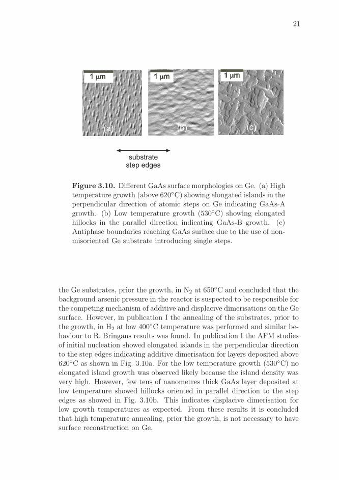
21
(b) (c)
1 mm 1 mm
substratestep edges
1 mm
(a)
Figure 3.10. Different GaAs surface morphologies on Ge. (a) Hightemperature growth (above 620◦C) showing elongated islands in theperpendicular direction of atomic steps on Ge indicating GaAs-Agrowth. (b) Low temperature growth (530◦C) showing elongatedhillocks in the parallel direction indicating GaAs-B growth. (c)Antiphase boundaries reaching GaAs surface due to the use of non-misoriented Ge substrate introducing single steps.
the Ge substrates, prior the growth, in N2 at 650◦C and concluded that thebackground arsenic pressure in the reactor is suspected to be responsible forthe competing mechanism of additive and displacive dimerisations on the Gesurface. However, in publication I the annealing of the substrates, prior tothe growth, in H2 at low 400◦C temperature was performed and similar be-haviour to R. Bringans results was found. In publication I the AFM studiesof initial nucleation showed elongated islands in the perpendicular directionto the step edges indicating additive dimerisation for layers deposited above620◦C as shown in Fig. 3.10a. For the low temperature growth (530◦C) noelongated island growth was observed likely because the island density wasvery high. However, few tens of nanometres thick GaAs layer deposited atlow temperature showed hillocks oriented in parallel direction to the stepedges as showed in Fig. 3.10b. This indicates displacive dimerisation forlow growth temperatures as expected. From these results it is concludedthat high temperature annealing, prior the growth, is not necessary to havesurface reconstruction on Ge.

22
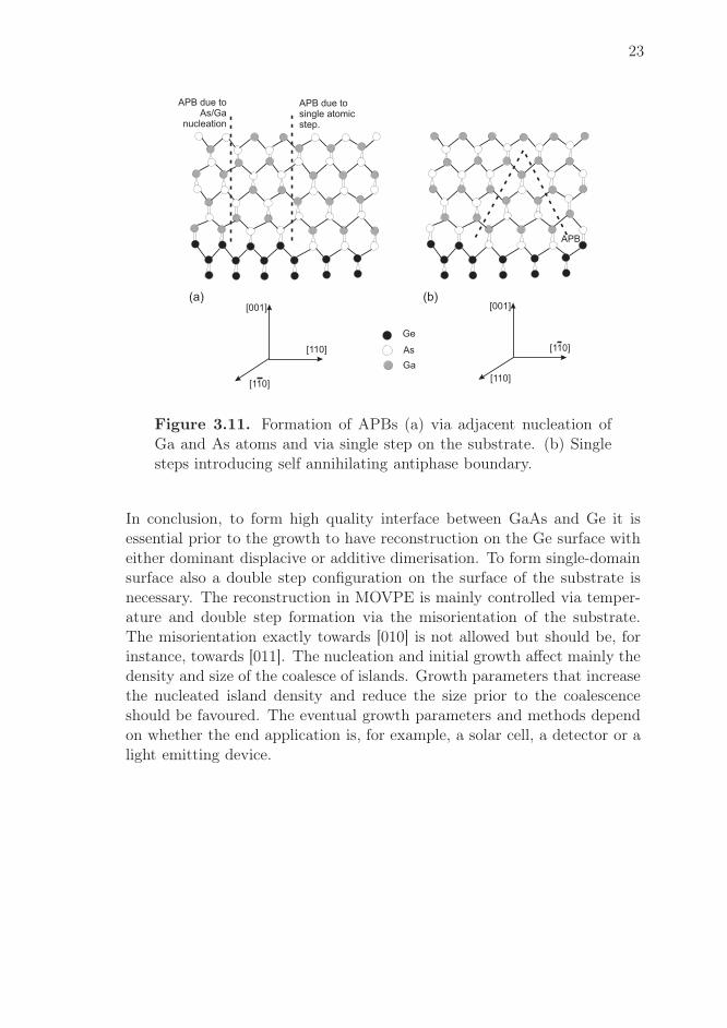
However, to have consistent As-As dimerisation on the surface is not enoughto produce antiphase boundary free crystal. The height of the surfacesteps on the substrate must be equivalent to even number (double) tohave the same atom on opposite sides of the step. R. Kaplan et al. [73],P. Pukite et al. [70] and J. Griffit et al. [71] stated that the step structureof Si and Ge substrates is formed by two monolayer steps (here monolayeris equivalent to 1/4 of the lattice constant of Ge or Si) and smooth terracesbetween them when the substrate is misorientated towards [011]. Notewor-thy is that for the substrates oriented exactly towards the [010] no dominantstep height could be determined. When grown on single step substrate thegrowth proceeds forming antiphase domains, which are brought together byAPBs consisting of Ga-Ga and As-As bonds. APBs are found to be electri-cally active defects and known to cause carrier scattering and nonradiativerecombination [9, 65]. In Fig. 3.11 two differently oriented APBs are pre-sented. An APB is formed if nucleation on Ge starts for one site from Gaand for the other site at the same step from As. Also if nucleation startsfrom equivalent atom but there exists a odd step height on the substratebetween them APB is formed. Formation of such APBs is indicated inFig. 3.11a. In such cases there exists an equal number of Ga-Ga bonds andAs-As bonds resulting in compensated structure. However, in Fig. 3.11bformation of an APB with localised As-As bonds is demonstrated, whichself-annihilates but results in donor-like behaviour.
An example of APBs on the surface of GaAs layer grown on a nonmisori-ented Ge substrate is presented in Fig. 3.10c, where clear boundaries arepresent. The APBs reach out trough the epitaxial layer to the samplesurface. The APBs are likely to form because a single step structure is ex-pected as the substrate has no misorientation. Due to the low growth ratethe surface is quite smooth and the area of APDs is quite large, hundredsof nanometers in width. In addition to the substrate misorientation severalother methods such as high group V partial pressure, low growth rate andhigh growth temperature are presented to lower the APBs density of polar-to-nonpolar epitaxy [17, 23, 74]. However, in publication I smooth surfacemorphology GaAs layers were grown at low temperature of 530◦C with verylow group V partial pressure introducing V/III input ratio of 3.5. Later alsosmooth surface morphology layers have been grown at 575◦C with also smallgroup V partial pressure. However, it was noticed in publication I that atgrowth temperatures above 620◦C it is essential to have high partial pres-sure introducing V/III ratio over 60 to achieve good surface morphology. Asit was stated that the surface dimerisation is changed around ∼ 600◦C theeffect of partial As pressure to the surface morphology for different dimerorientations is possible.
23
[001]
[110]
[110]
Ge
As
Ga
APB
APB due tosingle atomicstep.
[001]
[110]
[110]
APB due toAs/Ga
nucleation
(a) (b)
Figure 3.11. Formation of APBs (a) via adjacent nucleation ofGa and As atoms and via single step on the substrate. (b) Singlesteps introducing self annihilating antiphase boundary.
In conclusion, to form high quality interface between GaAs and Ge it isessential prior to the growth to have reconstruction on the Ge surface witheither dominant displacive or additive dimerisation. To form single-domainsurface also a double step configuration on the surface of the substrate isnecessary. The reconstruction in MOVPE is mainly controlled via temper-ature and double step formation via the misorientation of the substrate.The misorientation exactly towards [010] is not allowed but should be, forinstance, towards [011]. The nucleation and initial growth affect mainly thedensity and size of the coalesce of islands. Growth parameters that increasethe nucleated island density and reduce the size prior to the coalescenceshould be favoured. The eventual growth parameters and methods dependon whether the end application is, for example, a solar cell, a detector or alight emitting device.

4 Crystal properties and defects
4.1 Characterisation of tilted structures by X-ray
diffraction
H. Nagai showed that heteroepitaxy on misoriented substrates results in atilt angle α between (100) lattice planes of the epitaxial layer and the sub-strate [75]. The magnitude of the tilt is related to lattice constant separationand misorientation angle via tanα = (tanε)∆d/ds. Where ε is the misori-entation of the substrate, i.e., the angle between the Ge substrate surfaceand the Ge (100) lattice planes and ∆d is the lattice parameter difference inthe growth direction of the epitaxial layer (de) and substrate (ds) [75, 76].The tilt is built up to avoid formation of lattice defects at step interfaces asillustrated in Fig. 4.1. The misorientation of the substrate increases the stepdensity as terrace widths are decreased and results in larger tilt between thelattice planes. Correspondingly the relative difference between the latticeconstants determines the step height separation between the substrate andthe layer. In publication I X-ray diffraction was used to study tilt values ofGaAs layers grown on misoriented Ge.
High resolution X-ray diffraction (HRXRD) is an effective method to studycrystal quality, epitaxial composition, layer thicknesses, and relaxations ofsemiconductors. X-rays, having the photon energy of about 8 keV, penetrateinto the sample a depth of max 10 µm. The technique is a non-destructive,fast method to characterise the lattice structure. Fig 4.2 shows an photo-graph of the X-ray diffraction equipment used in this study. A schematiclayout of the high-resolution diffractometer with optics and specified anglesis illustrated in Fig. 4.3.
In the X-ray diffractometer only the Cu Kα1 (1.540553 Å) wavelength ispassed through a four-crystal Ge (220) monochromator [77]. The highlyparallel and monochromatic beam enters the sample at an angle ω, and
24

25
(100) Ge
substrate
(100) GaAs
epitaxy
a
Growthdirection
(100) Ge substrate
GaAs epitaxy(100)Growth direction
e
a
e
e
Ge surface
Figure 4.1. Formation of negative tilt of a GaAs epitaxial layergrown on a misoriented Ge substrate. The surface normals aredescribed by arrows. The misorientation ε and the tilt angle αcompared to the growth direction are presented.
Figure 4.2. Inside view of PANanalytic’s X’Pert PRO MRD highresolution X-ray diffraction system installed in Optoelectronics lab-oratory, Micronova.

26
X-r
ay
sourc
e
2q
f
y
monochromator
analyser
sample
open detector
triple axisdetector
mirror
misorientation (e)
w=q-e
(100) latticeplanes
Figure 4.3. Schematic layout of high resolution X-ray diffractionequipment including relevant components and adjustable angles.The diffraction plane is coincident with the paper surface.
the Bragg diffraction angle θ depends on the spacing between the latticeplanes. In a two-axis setup the signal is detected with an open detectorusing a large acceptance angle of about 1◦ for 2θ. However, because ofthe large acceptance angle, the open detector is unable to separate diffusescattering or small composition deviations. By using an analyser crystalin front of the detector, the acceptance angle can be reduced to 12 arcseconds for the 2θ angle [77]. This setup, the triple-axis configuration, alsoincreases the signal to noise ratio and enables resolution high enough forthe reciprocal space mapping of the samples. Reciprocal, or as presentedhere, angular space mapping is an effective method to study samples withtilts between the corresponding lattice planes.
When analysing heterostructures the layer thicknesses and compositions canbe found by comparing the measured ω − 2θ scan to simulated diffractioncurves. In the ω−2θ scan both the ω and 2θ are moved so that the relationω = θ − ε is valid, where ε is the misorientation angle of the substrate.However, if misorientation ε is present in the heterostructure, measuring theω − 2θ diffraction curve is complicated as there very likely is an additionaltilt α between the lattice planes of the substrate and the layer. In such acase two different relations ω = θ − ε and ω = θ − ε− α would be true forthe substrate and layer, respectively, and therefore no ω − 2θ scan couldeasily be performed simultaneously for the whole structure.

27
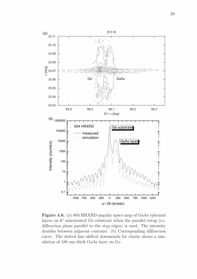
Fig. 4.4 shows a 004 angular space map of a GaAs epitaxial layer grownon a 6◦ towards 〈111〉 misoriented Ge substrate. The scan is performedin the perpendicular setup, where the step edges on the Ge surface are inthe direction of a diffraction plane normal (Fig. 4.5). The angular spacemap reveals a tilt angle α of about 0.007◦ between the GaAs and Ge (100)lattice planes. The grey horizontal line in the figure illustrates the situationwhere a single ω− 2θ scan with an analyser crystal would be performed forthe structure using the ω = θ − ε relation. As can be seen, no informationabout the epitaxial layer would be gained. If an open detector would beused, with an ∆ω acceptance angle of about 0.5◦, the measured ω−2θ curvewould result approximately in a projection of the intensity in the angularspace map to the x-axis. However, this projection would result in an untrueseparation between the substrate and layer peak [78]. H. Nagai studiedInGaAs layers deposited on misoriented GaAs substrates and stated that
2q \ w [deg]
w[d
eg]
[0 0 4]
65.9 66.0 66.1 66.2 66.3
27.00
27.01
27.02
27.03
27.04
27.05
27.06
27.07
27.08
27.09
GaAs
Gea = 0.007
Figure 4.4. 004 HRXRD angular space map of GaAs epitaxiallayers on 6◦ misoriented Ge substrate. The intensity doubles be-tween adjacent contours. The measurement is conducted in theperpendicular setup (i.e. the diffraction plane perpendicular to thestep edges). The amount of tilt α is found from the vertical dis-placement of the Ge and GaAs peaks. The gray line in the figurepresents information gained if a single high resolution diffractionscan would be performed in the same alignment.

28
(b)(a)
e
e-a
y=0 y= ey
diffractionplane
Perpendicularsetup
Parallelsetup
004 latticeplanes
Figure 4.5. High resolution XRD measurement setups. a) In theperpendicular setup (i.e. diffraction plane perpendicular to the stepedges) using ω = θ−ε relation. b) In the parallel setup (i.e. diffrac-tion plane parallel to the step edges) using ω = θ relation when the(ψ) angle of the sample is rotated to compensate ε. Later alignmentenables scans containing information of the whole structure.
the tilt is formed in the direction of the substrate misorientation and is notpresent for the perpendicular directions, i.e., in the direction of the stepedges [75, 79]. In publication I a similar orientation of the α was confirmedfor the GaAs/Ge structure. This result enables a single ω − 2θ scan in thetriple axis setup to display information of the whole structure, provided thatthe scan is performed in the parallel setup as illustrated in Fig. 4.5. In theparallel setup the diffraction plane lies in the direction of the step edges.The real layer thicknesses and compositions can then be obtained from asimulation. However, to perform such a scan the ψ and φ angles of thesample (indicated in the Fig. 4.3) must be rotated according to the amountand direction of the misorientation ε, respectively. In such an alignmentthe tilt has an minimal effect and results in an insignificant error. Fig. 4.6ashows a 004 angular space map of the same sample as in Fig. 4.4. The scanhas been performed in the parallel setup, thus no tilt is observed in themap as expected. In Fig. 4.6b a single 004 ω − 2θ diffraction curve scanperformed in the parallel alignment and a simulation of 188 nm thick GaAslayer on Ge are shown. The excellent agreement between measured andsimulated curves indicates nearly perfect crystal structure and the clarityof the fringes gives evidence of a high-quality interface between the Ge andGaAs materials.
29
2q \ w [deg]
w[d
eg
]
[0 0 4]
65.9 66.0 66.1 66.2 66.3
33.03
33.04
33.05
33.06
33.07
33.08
33.09
33.10
33.11
Ge GaAs
(a)
-1000 -750 -500 -250 0 250 500 750 1000 1250
0.1
1
10
100
1000
10000
100000
1000000(b)
GaAs layer
measured simulation
Inte
nsity
(co
unts
/s)
ω \ 2θ (arcsec)
Ge substrate004 HRXRD
Figure 4.6. (a) 004 HRXRD angular space map of GaAs epitaxiallayers on 6◦ misoriented Ge substrate when the parallel setup (i.e.diffraction plane parallel to the step edges) is used. The intensitydoubles between adjacent contours. (b) Corresponding diffractioncurve. The dotted line shifted downwards for clarity shows a sim-ulation of 188 nm thick GaAs layer on Ge.

30
4.2 Analysing defects using synchrotron X-ray to-
pography
Synchrotron X-ray topography (SXT) is used to image individual disloca-tions and to gain information about other extended defects. With fairlystraightforward analyses also the type and the Burgers vector of the dis-locations can be solved [80]. The very high intensity and the wide spec-trum of synchrotron radiation allow high resolution transmission and backreflection diffraction images of strongly absorbing materials using rela-tively short exposure times. The topography technique is very sensitiveto strain fields generated by different dislocations and even single misfitscan be revealed [81]. The topographs in this study were recorded in theHamburger Synchrotronstrahlungslabor HASYLAB using large-area trans-mission, large-area back-reflection, section transmission and section back-reflection geometry. Fig. 4.7 shows the schematic layout of the large-areaback-reflection topography technique. One incident and few of the numer-ous diffracted beams are drawn in the figure. Because the germanium sub-strates can be grown with very good quality, low dislocation and defect den-sities are enabled in the epitaxial layers. This was proven in publications Iand V wherein mixed type threading or circular arc dislocation density of250−500 cm−2 was determined from the topographs of a 650 nm thick GaAslayer. In contrast to a study by E. Müller no stacking faults were found inthe topographs [82]. The most common direction of the dislocations wasdetermined in publication I to be [1 0 1].
The overall dislocation density of GaAs on Ge is clearly less than what wasfound in high quality vapour pressure controlled Czochralski (VCz) grownGaAs substrates studied in publication IV showing a typical dislocation den-sity of 1500 cm−2. The strain relaxation mechanism of tensile GaAs on Gesubstrates was studied in publication V. Above critical thickness the strainrelaxes through misfit dislocations usually formed close to the interface ofthe mismatched layers [83]. Fig. 4.8 shows a misfit dislocation network of a750 nm thick GaAs layer on (001) Ge. The number of misfit dislocations ismeasured from the figure to about 500-600 adjacent dislocations/cm in thedirections of [1 1 0] and [1 1 0]. For a completely relaxed GaAs/Ge structurethe saturation misfit density is calculated to be 3.8 × 105 cm−1 [17]. Thevery small number of misfit dislocations of the 750 nm thick layer and theabsence of misfit dislocations in the 650 nm thick layer (in publication I)suggest a critical thickness of about 700 nm for a GaAs/Ge structure grownat low growth temperature of 575◦C. This value is above what is conven-

31
tionally expected for the 0.07 % mismatched GaAs/Ge system. However,because of the lower growth temperature the reduced thermal stress andthe formation of tilt via reorientation of the lattice planes are likely to en-hance the critical thickness [75, 84, 85]. It is observed from Fig. 4.8 that inthe [1 1 0] direction the dislocations are parallel to each other whereas in the[1 1 0] direction a small deviation angle exists between adjacent dislocations.This observation agrees with the results of Nijenhuis et al., as they con-cluded similar behaviour for GaAs layers grown on InGaAs substrates [86].Nijenhuis et al. stated that under tensile stress (as the GaAs/Ge system)a difference in the mobility between As and Ga dislocations can result in aasymmetrical strain relief at low growth temperatures. Formation of misfitdislocations was also studied in publication VI for GaAsN layers grown onGaAs substrates and later for GaAsN/GaAs/Ge systems, from which theresults are presented in chapter 5.
synchrotron
x-ray beam
sample
back reflection
topographs
206
026
film
117
117
117
1 17
Figure 4.7. Schematic layout of the large area back reflectiontopography technique, where the synchrotron X-ray radiation hitsthe sample through a hole in the film and forms several topographsof different lattice planes on the high resolution film.

32
g
[110]
[110]
Figure 4.8. 004 large area back reflection topograph of 750 nmthick GaAs epitaxial layer on (001) Ge showing misfit dislocationnetwork. Image size is 1.6 × 1.6 mm2 and the diffraction vector gprojection is marked with an arrow.
4.3 Optical characteristics and interfacial diffusion
In photoluminescence (PL) free carriers are excited into the material by op-tical excitation. General information on the material quality can be gainedas electronic transitions, in particular radiative recombinations of electron-hole pairs, are detected [87]. Several studies on luminescence of GaAs andGaAs/Ge heterostructures have been reported concerning band structureand n-type doping of GaAs as well as different shallow and deep levels inGaAs/Ge structures [88–90, 90–95]. In all studies a dominant peak nearthe band gap Eg of GaAs (1.519 eV at 0 K and 1.424 eV at room tempera-ture (RT)) can be found related to donor to valence band (VB) transitionassociated with germanium donor (GeGa) centres. In addition, at low tem-peratures below 77 K following transitions are recognised: around 1.48 eV aconduction band (CB) to germanium acceptor (GeAs) transition [93], around1.45 eV a GeAs to arsenic vacancy VAs transition [91, 94], around 1.41 eVa GeAs to interstitial arsenic atom (Asi) or GeAs to arsenic antisite (AsGa)[94] and a broad lower energy line around 1.2 eV corresponding to VGa
bound to GeGa [91]. The 1.2 eV luminescence is noticed only for the n-typesamples with the carrier concentration above 1 × 1018 cm−3. Also in thisstudy low energy luminescence was found for the Si doped n-GaAs layersused in the detector structures discussed in chapter 5. In addition, thelow energy luminescence could be found from some GaAs layers grown athigher temperatures, above 620◦C. This is due to the out-diffusion of Geinto the GaAs layer acting as a donor and introducing n-type doping into

33
the GaAs layer. The discussed transitions in the GaAs/Ge structures arepresented in Fig. 4.9, which shows low temperature (T=9 K) PL spectra ofundoped GaAs (TG = 620◦C, V/III = 60, t = 650 nm and n-type GaAs(TG = 620◦C, V/III = 60, t = 250 nm, n = 6× 1018 cm−3) layers grown onGe. The broadening of the luminescence spectrum with heavy n-type dopingis due to the band-filling of the CB and bandtailing as n-GaAs layer becomesdegenerate [96–98]. The out-diffusion of Ge into GaAs was also observed inthe secondary ion mass spectrometry studies in publication I, though thediffusion of As into Ge was found to be more significant. It was stated inpublication I that two different diffusion mechanisms are responsible for theAs diffusion into high-purity Ge: i) the concentration independent diffusionof As related to interstitial sites was found to cause high As concentrationclose to the GaAs/Ge interface and ii) the concentration dependent diffu-sion related to vacancies was found to extend deeper into Ge showing lowerAs concentration [99].
0.8 0.9 1.0 1.1 1.2 1.3 1.4 1.5 1.6 1.7
dopinginducedshift
VGa
-GeGa
VGa
-SiGa
GeGa
-VAs
CB-GeAs
GaAs n-GaAs
PL
inte
nsity
[a.u
.]
Photon energy [eV]
×25
VB-GeGa
Figure 4.9. Low temperature (T=9 K) photoluminescence froman undoped GaAs layer on Ge and from a Si doped n-GaAs layer onGe. The different transitions due to the impurities are identified.The peak around 1.45 eV of the undoped GaAs layer has beenmultiplied by 25 for clarity.

5 Applications
The germanium substrates have several applications in micro- and opto-electronics. GaInP/Ga(In)As/Ge three-junction solar cells with conversionefficiency around 31 % under space-solar spectrum (AM0, 1-sun) are amongthe most important applications currently in production [100–102]. Prior tothe three-junction solar cells in early 1990’s several scientific groups stud-ied single-junction cells based on the GaAs/Ge structure [19, 103, 104].After Weyers et al. [105] discovered the large band gap bowing effect ofGaAsN and Kondow et al. [106] introduced a novel GaInNAs compound,several propositions and studies of multi-junction solar cells were presentedon both GaAs and Ge substrates [107–110]. However, the difficulty of shortminority-carrier diffusion lengths in GaInNAs must still be overcome togain high, over 40 %, conversion efficiencies [111]. Light emitting diodes(LEDs), laser diodes and micro cavity LEDs on germanium have also beendemonstrated [112–114]. The results are well comparable and close to thosefrom the GaAs-based components, despite the fact that relatively little ef-fort have been placed into the research of light emitting components on Ge.However, expeditiously growing LED based lighting technology includingtraffic lights and tail lights for cars etc. demand lower costs. Ge providesa small strain reduction for the GaInNAs structures. The strain reductionusing intermediate layers is found to improve the optical quality of dilutenitride materials [115]. Also Ge has higher thermal conductivity than GaAsand enables more efficient cooling. However, the rather small band gap ofGe prevents bottom-emitting solutions for wavelengths below 1.88 µm fab-ricated on Ge which is transparent material only at longer wavelengths.Also high performance InAs Hall sensors have been epitaxially manufac-tured on Ge [116]. In radiation detectors Ge is widely used because ofits advantageous physical properties. The detector applications are moreclosely presented in chapter 5.1. In chapter 5.2 dilute nitride GaAsN layersand GaInNAs quantum well structures grown on Ge having luminescenceon telecommunication wavelengths are introduced.
34

35
5.1 Radiation detectors
In radiation detectors germanium is used as an intrinsic (i) region. Underreverse bias an electric field is used to deplete the i-region. Arriving pho-tons interact with Ge producing electrons and holes. The charge carriersare transported to the n- and p-electrodes and converted into a signal. Thegermanium detectors are particularly sensitive to high energy, i.e., shortwavelength radiation such as X-rays and gamma rays. Germanium is avail-able with very high crystal quality with a zero etch pit density (EPD) anda very low impurity concentration of the order of about 1010 cm−3. Thisenables long carrier lifetimes and full depletion with low bias voltages. Alsogood energy resolution can be obtained as Ge has low electron-hole paircreation energy due to the relative low band gap of 0.66 eV. High-puritygermanium is grown by the Czoralski-technique where the impurity con-centration is controlled via dislocation density. Too small a dislocationdensity (less than 100 cm−2) can hinder the annihilation of excess vacanciesduring the cooling after solidification and leads to hole trapping centres.Too large a dislocation density (more than 10000 cm−2) leads to chargetrapping by dislocations themselves. This is the reason that a higher dislo-cation density is often found in high-purity Ge substrates than in conven-tional ones. In radiation imaging often high-spatial resolution is requiredbut conventional germanium fabrication processes do not enable finely seg-mented structures [117]. A GaAs layer on Ge as an n- or p-type contactwould enable these finely segmented detector matrixes to be fabricated bypatterning the GaAs layers. Separate p- and n-type GaAs layers could begrown in the opposite sides of the Ge wafer to form a p-i-n structure. Theelectrical properties of the Ge-GaAs heterojunctions were already studiedin early 1960’s by R. Anderson by growing Ge on GaAs substrates [118].Later S. Strite et al. have studied the electrical properties of the Ge/GaAsstructures by growing Ge layers on GaAs substrates for transistor appli-cations [1] and M. Hudait et al. [119] studied MOVPE grown n-GaAs/n-Ge heterojunctions using Au-n-GaAs/n-Ge/Au-Ge/Au Schottky-junctions.Due to the relatively narrow band gap of Ge thermal generation of chargecarriers must be limited by cooling the detectors. Liquid nitrogen at thetemperature of 77 K is usually suitable to reduce the reverse-leakage cur-rent to an acceptable level. In publication VIII current-voltage (I-V) curvesfrom the detector matrixes were measured. N-type GaAs layers doped withSi were grown on Ge wafers and processed into pixel detector structures.The I-V measurements were performed by applying a voltage to the un-patterned bottom side with a Au contact and the pixel and a surroundingguard ring were hold at ground potential. Simultaneously the current from

36
the pixel was measured. Fig. 5.1 shows the structure and two measurementsperformed at room and at liquid nitrogen temperatures. At 77 K very lowleakage currents of about 10 pA were obtained for a 0.3 mm2 pixel at reversebias of 100 V.
However, for the detector structures the diffusion of As into the Ge substrateis problematic. Because very high-purity Ge material is used, the forma-tion of shallow As doped n-type germanium material in the direct vicin-ity of GaAs/Ge interface is quite unavoidable. In publications I and VIIIvery similar results concerning As diffusion into Ge were obtained from sec-ondary ion mass spectrometry and from I-V measurements as a function ofetching depth of the mesas. Low growth temperature was found to hinderthe concentration dependent diffusion effectively reducing the overall diffu-sion depth. However, concentration independent diffusion element was stillfound to cause high As concentrations very close to the interface. In ourrecent experiments arsenic has been appropriately diffused into Ge wafers inthe MOVPE reactor and the pixel structures have been manufactured intothis As-diffusion doped germanium. The detector resolution is measured tobe excellent 220 eV at 5.9 keV and 400 eV at 60 keV.
-80 -40 010-12
10-11
10-10
10-9
10-8
10-7
10-6
10-5
10-4
10-3
n-GaAsi-Ge
metallisation
294 K 77 K
Cur
rent
(A
)
Voltage (V)
metallisation
Figure 5.1. Schematic structure and I-V-curve of a GaAs/Gematrix detector pixel measured at room temperature and at liquidnitrogen temperature.

37
5.2 GaAs based nitride compounds on Ge
Incorporation of nitrogen into GaAs material affects differently on the phys-ical properties of GaAs than in conventional semiconductor alloys. Theunusually strong behaviour of the band gap Eg as the composition of N isaltered, know as band gap bowing effect enables telecommunication wave-lengths up to 1.55 µm using GaInNAs compounds [105, 106]. The bandgap of AByC1−y semiconductor compounds is well described by the equa-tion 5.1. For the most semiconductor compounds the band gap change fromthe AB properties to the AC properties is almost linear and the bowing pa-rameter b is less than 1 eV. However, for the GaInNyAs1−y compound b iscomposition dependent and is of the order of 25 eV below y<0.01 and about16 eV for larger values of y [120–122].
E(AByC1−y) = (1 − y)EAC + yEAB − by(1 − y) (5.1)
Already a small amount, less than 1 %, of nitrogen causes a large redshiftto the band gap, increases the effective electron mass [123, 124] and de-creases the electron mobility of GaAs [111]. These anomalous propertiesof dilute nitride layers are understood through large electronegativity andsize differences of As and N atoms. The covalent radii are 0.12 nm and0.07 nm for As and N, respectively. The larger electronegativity of a ni-trogen atom compared to As makes the Ga-N bond more polar favouringelectron localisation around the nitrogen atom.
Fig. 5.2 illustrates the band gap vs. the lattice constant of relevant semi-conductor materials including GaN compound. Only the variation of Eg forGaAs1−yNy and Ga1−xInxNyAs1−y compounds are shown by bowed lines forclarity. The figure shows that Ga1−xInxNyAs1−y material can be grown onGe substrates lattice matched, compressively strained or tensile strained.However, difficulties arise as the solubility of nitrogen into GaAs basedcompounds is very limited [105, 125]. The growth of lattice matched layers(x ≈ 3y) is especially important for solar cell structures on Ge [108, 126] andon GaAs [109], as thick layers are necessary. For long wavelength (1.3 µm)laser components compressively strained Ga1−xInxNyAs1−y QW layers withx ∼ 10− 35 % and y ∼ 1− 3 % on GaAs are successfully used [127–131]. Inpublication VII new approach achieve long wavelengths using dilute nitrideQWs on Ge was introduced.
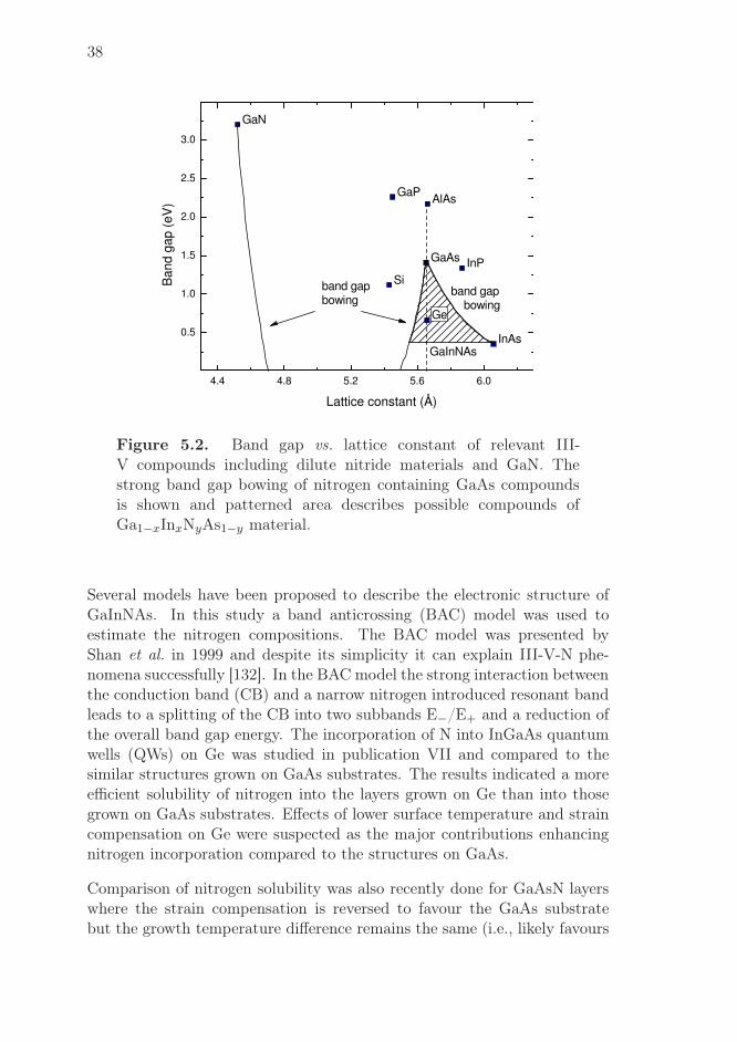
38
4.4 4.8 5.2 5.6 6.0
0.5
1.0
1.5
2.0
2.5
3.0
Ge
Si
GaAs
GaN
InAs
InP
AlAsGaP
Lattice constant (Å)
band gapbowing
band gap bowing
Ban
d ga
p (e
V)
GaInNAs
Ge
Figure 5.2. Band gap vs. lattice constant of relevant III-V compounds including dilute nitride materials and GaN. Thestrong band gap bowing of nitrogen containing GaAs compoundsis shown and patterned area describes possible compounds ofGa1−xInxNyAs1−y material.
Several models have been proposed to describe the electronic structure ofGaInNAs. In this study a band anticrossing (BAC) model was used toestimate the nitrogen compositions. The BAC model was presented byShan et al. in 1999 and despite its simplicity it can explain III-V-N phe-nomena successfully [132]. In the BAC model the strong interaction betweenthe conduction band (CB) and a narrow nitrogen introduced resonant bandleads to a splitting of the CB into two subbands E−/E+ and a reduction ofthe overall band gap energy. The incorporation of N into InGaAs quantumwells (QWs) on Ge was studied in publication VII and compared to thesimilar structures grown on GaAs substrates. The results indicated a moreefficient solubility of nitrogen into the layers grown on Ge than into thosegrown on GaAs substrates. Effects of lower surface temperature and straincompensation on Ge were suspected as the major contributions enhancingnitrogen incorporation compared to the structures on GaAs.
Comparison of nitrogen solubility was also recently done for GaAsN layerswhere the strain compensation is reversed to favour the GaAs substratebut the growth temperature difference remains the same (i.e., likely favours

39
2q \ w [deg]
w[d
eg
]
[0 0 4]
66.00 66.05 66.10 66.15 66.20 66.25 66.30
32.98
33.00
33.02
33.04
33.06
33.08
33.10
GaAsNGaAsGe
Figure 5.3. 004 angular space map of GaAs-GaAs0.996N0.004 struc-ture grown on misoriented Ge substrate measured the step edgesparallel to the diffraction plane (i.e. parallel setup). The intensitydoubles between adjacent contours.
the Ge substrate). The studies strengthen the previous proposals as nomeasurable difference of nitrogen incorporation was noticed for the Ge andGaAs substrates. Fig. 5.3 shows a 004 angular space map and Fig. 5.4shows a 004 ω − 2θ diffraction curve of a studied GaAs-GaAsN structuregrown on Ge. Both measurements were done in the direction of the stepedges ,i.e., parallel X-ray diffraction setup. Fig. 5.4 also shows a 004 ω− 2θdiffraction curves of the same structure grown simultaneously on GaAs anda simulation of GaAs0.996N0.004/GaAs/Ge structure with layer thicknessesof 364 nm and 285 nm, respectively.
In publication VI creation of misfit dislocations on GaAsN layers as functionof the N composition and layer thickness on GaAs substrates was studied.For a 500 nm thick GaAsN layer on GaAs with nitrogen content of 0.9 %few misfit dislocations were detected. However, when grown on Ge similaramount of misfit dislocations were observed for the GaAsN/GaAs/Ge struc-ture with nitrogen content of 0.4 % and GaAsN layer thicknesses of 364 nm.This is due to the additional strain induced both by the Ge substrate andthe 285 nm thick GaAs buffer.

40
-300 -150 0 150 300 450 600 750
GaAssubstrate
GaAs0.996
N0.004
GaAs buffer measured simulation
Inte
nsity
(co
unts
/s)
ω \ 2θ (arcsec)
Ge substrate004 HRXRD
Figure 5.4. Topmost curve shows a 004 HRXRD diffraction curveof the GaAs-GaAsN epitaxial layer on misoriented Ge substratemeasured in the parallel setup. The dotted line shifted downwardsfor clarity shows a simulation of a 285 nm thick GaAs and a 364 nmthick GaAs0.996N0.004 layer on Ge. In addition, the lowest curveshows an 004 HRXRD diffraction curve of the structure on a GaAssubstrate.
The growth of the GaInNAs QW in publication VII was performed us-ing two MOVPE equipments. A GaAs buffer was grown in the 3×2" ver-tical CCS reactor and the dilute nitride layers in the horizontal reactor.The following results were completed using the CCS reactor and performedentirely in a single growth run. The growth cycles consist of a 200 nmthick GaAs buffer and 3×Ga0.83In0.17NyAs1−y/GaAs (6 nm/15 nm) QWstructure grown at 575◦C. The results concerning nitrogen incorporationefficiency favouring Ge over GaAs were well congruent with the results pre-sented in publication VII. Fig. 5.5 shows room temperature PL measure-ments of the Ga0.83In0.17NyAs1−y multi-QW structures with different nitro-gen contents. Intensities have been scaled to make the figure clearer and thescaling factors are shown below each spectrum. The indium content of thesamples was determined from XRD analyses to about 17 %. The spectrumof the InGaAs sample on the right shows the narrowest spectral width butthe highest intensity is observed from the nitrogen sample with low nitrogencontent. This is due to the larger conduction band offset, which provides a

41
0.7 0.8 0.9 1.0 1.1 1.2 1.3 1.4
x8
1.4 µm
1.31 µm
1.29 µm
1.12 µm 0.97 µm
PL
inte
nsity
(a.
u.)
x4
Photon energy (eV)
x3
x1
x2
1.56 µm
x15
Figure 5.5. Room temperature photoluminescence of three 6 nmthick Ga0.83In0.17NxAs1−x quantum wells with 15 nm thick GaAsbarrier grown on Ge with 190 nm thick GaAs buffer. The x variesfrom 0 to about 0.05. Different factors have been used to makefigure clearer and are shown within each spectrum.
higher quantum confinement in a GaInNAs QW than in a InGaAs QW [133].As more nitrogen is introduced, the spectra are redshifted and due to theincreased density of crystal defects the PL intensity is decreased [134].
In Fig. 5.6 the nitrogen content vs. PL photon energy is showed for theGa0.83In0.17NxAs1−x samples. The nitrogen content was estimated fromthe BAC model. Also the samples discussed in publication VII with theindium content of 20 % are shown in the figure. The sample with pho-ton energy of about 0.79 eV, (i.e. 1.56 µm) shows nitrogen incorporationof about 5 %. The nitrogen content is considered fairly high because inthe MOVPE technique the incorporation of nitrogen into InGaAs layers iseven more difficult than into the GaAs layers. The overall reason for thelow incorporation efficiency of nitrogen into InGaAs is suspected to be thesurface segregation of indium that creates surface layer with excess indiumenhancing desorption of nitrogen adatoms [126, 135]. Fig. 5.7 shows theeffect of the DMHz/TBAs molar flow ratio on the nitrogen incorporation.The relative TBAs/III molar flow ratio is also shown in the parenthesesnext to each data point in the figure. With higher DMHz flows a smallerTBAs/III molar flow ratio is enough to protect the surface. This enablesraising the DMHz/TBAs molar flow ratio by decreasing the TBAs flow.However, GaInNAs layers have a very narrow growth window for V/III in-

42
0.0 1.0 2.0 3.0 4.0 5.0
0.8
0.9
1.0
1.1
1.2
1.3 17 % In corporation 20 % In corporation
Pho
ton
ener
gy (
eV)
Nitrogen (%)
Figure 5.6. Calculated nitrogen contents using BAC model vs.photon energy of GaInNAs quantum wells grown on Ge. The strainfor the calculations is derived from the HRXRD measurement.
0.89 0.90 0.91 0.92 0.93 0.94 0.950.0
1.0
2.0
3.0
4.0
5.0
(3.9)(3.9)(3.9)
(2.7)
(3.4)
(3.4)
(3.3)
17 % In corporation 20 % In corporation
Nitr
ogen
con
tent
(%
)
DMHz/V molar flow ratio
(3.3)
( ) TBAs/III molar flow ratio
Figure 5.7. Effect of DMHz/V molar flow ratio into nitrogen in-corporation in GaInNAs quantum wells grown on Ge. The nitrogenincorporation is derived from the BAC model.
put ratio [134]. In our experiment decreasing the TBAs/III molar flow ratiobelow 2.5 caused poor crystal quality due to too weak surface protection. Itis noteworthy that to introduce few percentages of nitrogen into the layerover 90 % of the total group V gas flow has to be DMHz.

6 Summary
The growth of compound semiconductors on Ge substrates using MOVPEtechnique was studied. Nucleation and initial growth phases of InAs, In-GaAs and GaAs were inspected by AFM. The growth of GaAs on Ge be-gins by forming three-dimensional islands, which coalesce and form two-dimensional layer if the growth is continued. By adjusting the growth pa-rameters the size, density and uniformity of the coalescence islands can beaffected. Significant effort was conducted into optimisations of the growthparameters that favour high areal density and uniformity of the island. Theisland density has exponential dependency on the growth temperature andis most effectively enhanced by lowering the growth temperature. Usinggrowth temperature below 550◦C high island densities over 1010 cm−3 canbe obtained. For the high island density the coalescence of the GaAs is-lands occurs at small and uniform size and smooth two-dimensional surfaceis obtained already with small layer thicknesses. To achieve the optimisedgrowth conditions also the input V/III ratio and the growth rate must becarefully chosen. The growth temperature also effects the reconstruction ofthe germanium surface by controlling the dimerisation. Additive dimerisa-tion is found for the growths initiated above about 600◦C and displacivefor the growths initiated at lower temperatures. The formation of APDs isprevented if one dimerisation is dominant and the Ge surface has a doublestep configuration. The double step configuration is obtained using a fewdegrees misoriented substrate towards 〈111〉.
The detailed HRXRD analyses of GaAs/Ge (100) heterostructures are com-plicated due to the formation of the tilt angle between the (100) latticeplanes of Ge and epitaxial GaAs. However, using the parallel setup, pre-sented in this work, scans containing information of the whole structureare successfully obtained. In the parallel setup the X-ray diffraction planeis parallel to the step edges of the Ge substrate and the sample is rotatedin the direction of the step edges normal according to the amount of themisorientation. In the HRXRD and in the synchrotron X-ray topographyanalyses the crystal quality of the grown GaAs/Ge structures was found
43

44
nearly perfect and a very low dislocation density of 250 − 500 cm−2 wasmeasured from the topographs of a 650 nm thick GaAs layer. GaAs andGe have a small lattice constant separation of 0.07 % resulting in strainbetween Ge and GaAs layer. Small number of misfit dislocations was foundin the SXT analyses for the 750 nm thick GaAs layer grown at low growthtemperature of 575◦C. The critical thickness of about 700 nm is above whatis conventionally expected for the GaAs/Ge system. The enhancement inthe critical thickness is because of the low growth temperature resulting insmaller thermal stress.
Germanium is an excellent material choice for short wavelength detectorapplications due to its physical properties and to its availability to fabri-cate as a very high-purity material. However, conventional manufacturingprocesses do not alloy finely segmented detector structures on Ge. To gainsuch novel structures arsenic was appropriately diffused into the Ge wafersin the MOVPE reactor. This enables manufacturing the pixel matrices intogermanium. The pixel detector resolution is measured to be as excellent as220 eV and 400 eV at 5.9 keV and 60 keV, respectively.
The incorporation efficiency of N into GaInAsN quantum well layers is verylow. However, in the new approach were Ge substrates are used instead ofGaAs substrates the incorporation efficiency of N was found to be more ef-fective. This enhancement results from the small strain compensation intro-duced by Ge. The low growth temperature of 575◦C and the low TBAs/IIIratio of 2.7 were used to obtain the long wavelength luminescence maximum1.56 µm from Ga1−yInyNxAs1−x QWs on Ge with a In composition y = 0.17and a high N composition x = 0.05.

References
[1] S. Strite, M. Ünlü, K. Adomi, G.-B. Gao, A. Agarwal, A. Rockett,H. Morkoç, D. Li, Y. Nakamura and N. Otsuka, GaAs/Ge/GaAsheterostructure by molecular beam epitaxy, J. Vac. Sci. Technol. B 81131–1140 (1990).
[2] N. Wu, Q. Zhang, C. Zhu, D. Chan, M. Li, N. Balasubramanian,A. Chin and D.-L. Kwong, Alternative surface passivation on ger-manium for metal-oxide-semiconductor applications with high-k gatedielectric, Appl. Phys. Lett. 85 4127–4129 (2004).
[3] H. Shang, H. Okorn-Schimdt, J. Ott, P. Kozlowski, S. Steen, E. Jones,H. Wong and W. Hanesch, Electrical Characterization of Germaniump-Channel MOSFETs, IEEE Electron Device Lett. 24 242–244 (2003).
[4] C. Chui, S. Ramanathan, B. Triplett, P. McIntyre and K. Saraswat,Germanium MOS Capacitors Incorporating Ultrathin High-k Gate Di-electric, IEEE Electron Device Lett. 23 473–475 (2002).
[5] D. Schreurs, C. van Niekerk, R. Vandersmissen and G. Borghs, Devel-opment of Extraction and Optimization Based Large-Signal Models forThinned Metamorphic High- Electron Mobility Transistors on Germa-nium, Int. J. RF and Microwave CAE 12 439–447 (2002).
[6] R. Fischer, H. Morkoç, D. A. Neumann, H. Zabel, C. Choi, N. Otsuka,M. Longerbone and L. Erickson, Material properties of high-qualityGaAs epitaxial layers grown on Si substrates, J. Appl. Phys. 60 1640–1647 (1986).
[7] T. Ueda, S. Nishi, Y. Kawarada, M. Akiyama and K. Kaminishi,Effects of the Substrate Offset Angle on the Growth of GaAs on SiSubstrate, Jpn. J. Appl. Phys. 25 L789–L791 (1986).
45

46
[8] D. Biegelsen, F. Ponce, A. Smith and J. Tramontana, Initial stagesof epitaxial growth of GaAs on (100) silicon, J. Appl. Phys. 61 1856–1859 (1987).
[9] H. Noge, H. Kano, M. Hashimoto and I. Igarashi, Antiphase domainsin GaAs grown on a (001)-oriented Si substrate by molecular-beamepitaxy, J. Appl. Phys. 64 2246–2248 (1988).
[10] S. Onozawa, T. Uedo and masahiro Akiyama, Initial Stage of MOCVDGrowth of GaAs on Si, J. Cryst. Growth 93 443–448 (1988).
[11] T. Soga, T. George, T. Jimbo and M. Umeno, Initial Growth Mech-anism for GaAs and GaP on Si Substrate by Metalorganic ChemicalVapor Deposition, Jpn. J. Appl. Phys. 30 3471–3474 (1991).
[12] M. Currie, S. Samavedam, T. Langdo, C. Leitz and E. Fitzgerald,Controlling threading dislocation densities in Ge on Si using gradedSiGe layers and chemical-mechanical polishing, Appl. Phys. Lett. 721718–1720 (1998).
[13] C. Andre, J. Boeckl, C. Leitz, M. Currie, T. Langdo, E. Fitzgerald andS. Ringel, Low-temperature GaAs films grown on Ge and Ge/SiGe/Sisubstrates, J. Appl. Phys. 94 4980–4985 (2003).
[14] J. Carlin, S. Ringel, E. Fitzgerald, M. Bulsara and B. Keyes, Impact ofGaAs buffer thickness on electronic quality of GaAs grown on gradedGe/GeSi/Si substrates, Appl. Phys. Lett. 76 1884–1886 (2000).
[15] N. Chand, J. Klem, T. Henderson and H. Morkoç, Diffusion of Asand Ge during growth of GaAs on Ge substrate by molecular beamepitaxy: Its effect on the device electrical characterics, J. Appl. Phys59 3601–3604 (1986).
[16] P. Modak, M. Hudait, S. Hardikar and S. Krupanidhi, OMVPEgrowth of undoped and Si-doped GaAs epitaxial layers on Ge, J. Cryst.Growth 193 501–509 (1998).
[17] G. Timo, C. Flores, B. Bollani, D. Passoni, C. Bocchi, P. Franzosi,L. Lazzarini and G. Salviati, The effect of the growth rate on the lowpressure metalorganic vapour phase epitaxy of GaAs/Ge heterostruc-tures, J. Cryst. Growth 125 440–448 (1992).
[18] R. Fischer, W. Masselink, J. Klem, T. Henderson, T. McGlinn,H. Morkoç, J. Mazur and J. Washburn, Growth and properties ofGaAs/AlGaAs on nonpolar substrates using molecular beam epitaxy,J. Appl. Phys. 58 374–381 (1985).

47
[19] P. Iles, Y.-C. M. Yeh, F. Ho, C.-L. Chu and C. Cheng, High-Efficiency(>20% AMO) GaAs Solar Cells Grown on Inactive-Ge substrates,IEEE Electron Device Lett. 11 140–142 (1990).
[20] J. Chen, M. L. Ristow, J. Cubbage and J. Werthen, Effects of metalor-ganic chemical vapor deposition growth conditions on the GaAs/Gesolar cell properties, Appl. Phys. Lett. 58 2282–2284 (1991).
[21] Y. Li, L. Lazzarini, L. Giling and G. Salviati, On the sublattice locationof GaAs grown on Ge, J. Appl. Phys. 76 5748–5753 (1994).
[22] Y. Li, G. Salviati, M. Bongers, L. Lazzarini, L. Nasi and L. Giling,On the formation of antiphase domains in the system of GaAs on Ge,J. Cryst. Growth 163 195–202 (1996).
[23] Y. Li and L. Giling, A closer study on the self-annihilation of an-tiphase boundaries in GaAs epilayers, J. Cryst. Growth 163 203–211(1996).
[24] L. Lazzarini, L. Nasi, G. Salviati, C. Fregonara, Y. Li, L. Giling,C. Hardingham and D. Holt, Antiphase disorder in GaAs/Ge het-erostructure for solar cells, Micron 31 217–222 (2000).
[25] M. Hudait and S. Krupanidhi, Atomic force microscopy study of sur-face morphology in Si-doped epi-GaaAs on Ge substrates: effect of offorientation, Materials Research Bulletin 35 909–919 (2000).
[26] N. Cho and C. Carter, Formation faceting and interaction behaviorsof antiphase boundaries in GaAs thin films, J. Materials Science 364209–4222 (2001).
[27] R. Tyagi, M. Singh, M. Thirumavalavan, T. Srinivasan and S. Agar-wal, The Influence of As and Ga Prelayers on the Metal-OrganicChemical Vapor Deposition of GaAs/Ge, J. Elect. Mat. 31 234–237(2002).
[28] M. Hudait and S. Krupanidhi, Self-annihilation of antiphase bound-aries in GaAs epilayers on Ge substrates grown by metal-organicvapor-phase epitaxy, J. Appl. Phys. 89 5972–5979 (2001).
[29] J. Derluyn, K. Dessein, G. Flamand, Y. Mols, J. Poortmans,G. Borghs and I. Moerman, Comparison of MOVPE grown GaAssolar cells using different substrates and group-V precursors, J. Cryst.Growth 247 237–244 (2003).

48
[30] C.-A. Chang, Interface morphology of epitaxial growth of Ge on GaAsand GaAs on Ge by molecular beam epitaxy, J. Appl. Phys. 53 1253–1255 (1982).
[31] J. Neave, P. Larsen, B. Joyce, J. Gowers and J. van der Veen, Some ob-servations on Ge:GaAs(001) and GaAs:Ge(001) interfaces and films,J. Vac. Sci. Technol. B 1 668–674 (1983).
[32] P. Petroff, Nucleation and growth of GaAs on Ge and the structure ofantiphase boundaries, J. Vac. Sci. Technol. B 4 874–877 (1986).
[33] S. Strite, D. Biswas, K. Adomi and H. Morkoç, Study of sublatticeorientation of GaAs on Ge, J. Appl. Phys. 67 1609–1612 (1990).
[34] E. Fitzgerald, J. Kuo, Y. Xie and P. Silverman, Necessity of Gaprelayers in GaAs/Ge growth using gas-source molecular beam epi-taxy, Appl. Phys. Lett. 64 733–735 (1994).
[35] S. Ting, E. Fitzgerald, R. Sieg and S. Ringel, Range of Defect Mor-phologies on GaAs Grown on Offcut (001) Ge Substrates, J. Elect.Mat. 27 451–461 (1998).
[36] A. Gutakovsky, A. Katkov, M. Kotkov, O. Pcheluakov andM. Revenko, Effect of Ga predeposition layer on the growth of GaAsvicinal Ge(001), J. Cryst. Growth 201/202 232–235 (1999).
[37] W. Li, S. Laaksonen, J. Haapamaa and M. Pessa, Growth of device-quality GaAs layer directly on (001) Ge substrates by both solid-sourceand gas-source MBE, J. Cryst Growth 227-228 104–107 (2001).
[38] A. Wan, V. Menon, S. Forrest, D. Wasserman, S. Lyon and A. Kahn,Characterization of GaAs grown by molecular beam epitaxy on vicinalGe(100) substrates, J. Vac. Sci. Technol. B 22 1893–1898 (2004).
[39] H. Manasevit, Single-crystal gallium arsenide on insulating substrates,Appl. Phys. Lett. 12 156–159 (1968).
[40] C. Larsen, N. Buchan, S. Li and G. Stringfellow, Decomposition mech-anism of tertiarybutylarsine, J. Cryst. Growth 94 663–672 (1989).
[41] A. Jones, Metalorganic precursors for vapour phase epitaxy, J. Cryst.Growth 129 728–773 (1993).
[42] F. Salomonsson, C. Asplund, S. Mogg, G. Plaine, P. Sundgren andM. Hammar, Low-treshold high-temperature operation of 1.2 µm In-GaAs vertical cavity lasers, Electron. Lett. 37 957–958 (2001).

49
[43] A. Moto, S. Tanaka, N. Ikoma, T. Tanabe, S. Takagishi, M. Takag-ishi and T. Katsuyama, Metalorganic Vapor Phase Epitaxial Growthof GaNAs Using Tertiarybutylarsine (TBA) and Dimethylhydrazine(DMHy), Jpn. J. Appl. Phys. 38 1015–1018 (1999).
[44] G. Solomon, J. Trezza and J. Harris, Substrate temperature and mono-layer coverage effects on epitaxial ordering of InAs and InGaAs islandson GaAs, Appl. Phys. Lett. 66 991–993 (1995).
[45] J. Oshinowo, M. Nishioka, S. Ishida and Y. Arakawa, Highly uniformInGaAs/GaAs quantum dots (∼15 nm) by metalorganic chemical va-por deposition, Appl. Phys. Lett. 65 1421–1423 (1994).
[46] N. Ledentsov, J. Böhrer, D. Bimberg, I. Kochnev, M. V. Maxi-mov, P. Kop’ev, Z. Alferov, A. Kosogov, S. Ruvimov, P. Werner andU. Gösele, Formation of coherent superdots using metal-organic chem-ical vapor deposition, Appl. Phys. Lett. 69 1095–1097 (1996).
[47] F. Heinrichsdorff, A. Krost, N. K. abd Ming-Hua Mao, M. Grund-mann, D. Bimberg, A. Olegovich and P. Werner, InAs/GaAs Quan-tum Dots Grown by Metalorganic Chemical Vapor Deposition, Jpn. J.Appl. Phys. 36 4129–4133 (1997).
[48] R. Leon, C. Lobo, J. Zou, T. Romeo and D. Cockayne, Stable andmetastable InGaAs/GaAs Island Shapes and Surfactantlike Suppres-sion of the Wetting Transformation, Phys. Rev. Lett. 81 2486–2489(1998).
[49] A. Passaseo, R. Rinaldi, M. Longo, S. Antonaci, A. Convertino,R. Cingolani, A. Taurino and M. Catalano, Structural study of In-GaAs/GaAs quantum dots grown by metalorganic chemical vapor de-position for optoelectronic applications at 1.3 µm, J. Appl. Phys. 894341–4348 (2001).
[50] J. Moison, F. Houzay, F. Barthe, L. Leprince, E. Andre and O. Vatel,Self-organized growth of regular nanometer-scale InAs dots on GaAs,Appl. Phys. Lett. 64 196–198 (1994).
[51] O. Brandt, L. Tapfer, K. Ploog, R. Bierwolf, M. Hohenstein,F. Philipp, H. Lage and A. Heberle, InA quantum dots in a single-crystal GaAs matrix, Phys. Rev. B 44 8044–8053 (1991).
[52] D. Leonard, M. Krishnamurthy, C. Reaves, S. Denbaars and P. Petroff,Direct formation of quantum-sized dots from uniform coherent islandsof InGaAs on GaAs surfaces, Appl. Phys. Lett. 63 3203–3205 (1993).

50
[53] N. Ledentsov, V. Shchukin, M. Grundmann, N. Kirstaedter, J. Böhrer,O. Schmidt, D. Bimberg, V. Ustinov, A. Egorov, A. Zhukov,P. Kop’ev, S. Zaitsev, N. Gordeev, Z. Alferov, A. Borovkov, A. Koso-gov, S. Ruvimov, P. Werner, U. Güsele and J. Heydenreich, Directformation of vertically coupled quantum dots in Stranski-Krastanowgrowth, Phys. Rev. B 54 8743–8750 (1996).
[54] Y. Sugiyama, Y. Nakata, K. Imamura, S. Muto and N. Yokoyama,Stacked InAs Self-Assembled Quantum Dots on (001) GaAs grown bymolecular beam epitaxy, Jpn. J. Appl. Phys. 35 1320–1324 (1996).
[55] M. Colocci, F. Bogani, L. Carraresi, R. Mattolini, A. Bosacchi,S. Franchi, P. Frigeri, M. Rosa-Clot and S. Taddei, Growth patterns ofself-assembled InAs quantum dots near the two-dimensional to three-dimensional transition, Appl. Phys. Lett. 70 3140–3142 (1997).
[56] J. Marquez, L. Geelhaar and K. Jacobi, Atomically resolved structureof InAs quantum dots, Appl. Phys. Lett. 78 2309–2311 (2001).
[57] K. Jacobi, Atomic structure of InAs quantum dots on GaAs, Progressin Surface Science 71 185–215 (2003).
[58] D. Leonard, K. Pond and P. Petroff, Critical layer thickness for self-assembled InAs islands on GaAs, Phys. Rev. B 50 11687 (1994).
[59] T. Soga, T. Suzuki, M. Mori, T. Jimbo and M. Umeno, The effects ofthe growth parameters on the initial stage of epitaxial growth of GaPon Si by metalorganic chemical vapor depositon, J. Cryst. Growth132 134–140 (1993).
[60] T. Suzuki, T. Soga, T. Jimbo and M. Umeno, Growth mechanism ofGaP on Si by MOVPE, J. Cryst. Growth 115 158–163 (1991).
[61] Y.-W. Mo, D. Savage, B. Swartzentruber and M. Lagally, KineticPathway in Stranski-Krastanov Growth of Ge on Si(001), Phys. Rev.Lett. 65 1020–1023 (1990).
[62] Z. Gai, W. Yang, T. Sakurai and R. Zhao, Heteroepitaxy of germaniumon Si(103) and stable surfaces of germanium, Phys. Rev. B 59 13009–13013 (1999).
[63] L. Bobb, H. Holloway, K. Maxwell and E. Zimmerman, Orientedgrowth of Semiconductors. III. Growth of Gallium Arsenide on Ger-manium, J. Appl. Phys. 37 4687–4693 (1966).

51
[64] K. Mizuguchi, N. Hayafuji, S. Ochi, T. Murotani and K. Fujikawa,MOCVD GaAs growth on Ge (100) and Si (100) substrates, J. Cryst.Growth 77 509–514 (1986).
[65] H. Kroemer, Polar-on-nonpolar epitaxy, J. Cryst. Growth 81 193–204(1987).
[66] M. Kawabe, T. Ueda and H. Takasugi, Initial Stage and DomainStructure of GaAs Grown on Si(100) by molecular Beam Epitaxy, Jpn.J. Appl Phys. 26 L114–L116 (1987).
[67] J. Varrio, H. Asonen, J. Lammasniemi, K. Rakennus and M. Pessa,Model of growth of single-domain GaAs layers on double-domain Sisubstrates by molecular beam epitaxy, Appl. Phys. Lett. 55 1987–1989(1989).
[68] R. Bringans, D. Biegelsen and L.-E. Swartz, Atomic-step rearrange-ment on Si(100) by interaction with arsenic and the implication forGaAs-on-Si epitaxy, Phys. Rev. B 44 3054–3063 (1991).
[69] S. Ting and E. Fitzgerald, Metal-organic chemical vapor depositionof single domain GaAs on Ge/GeSi/Si and Ge substrates, J. Appl.Phys. 87 2618–2628 (2000).
[70] P. Pukite and P. Cohen, Supression of antiphase domains in thegrowth of GaAs on Ge(100) by molecular beam epitaxy, J. Cryst.Growth 81 214–220 (1987).
[71] J. Griffit, J. Kubby, P. Wierenga, R. Becker and J. Vickers, Tunnelingmicroscopy of steps on vicinal Ge(001) and Si(001) surfaces, J. Vac.Sci. Technol. A 6 493–496 (1988).
[72] I. Kamiya, D. Aspnes, H. Tanaka, L. Florez, J. Harbison and R. Bhat,Surface Science at Atmospheric Pressure: Reconstructions on (001)GaAs in organometallic Chemical Vapor Deposition, Phys. Rev. Lett.68 627–631 (1992).
[73] R. Kaplan, LEED study of the stepped surface of vicinal Si (100),Surface Science 93 145–158 (1980).
[74] M. Bongers, Y. Li, J. te Nijenhuis and L. Giling, Structural analysisof InxGa1−xAs grown on Ge by low pressure metalorganic chemicalvapour deposition, J. Cryst. Growth 162 7–14 (1996).
[75] H. Nagai, Structure of vapor-deposited GaInAs crystals, J. Appl.Phys. 45 3789–3794 (1974).

52
[76] P. Auvray, M. Baudet and A. Regreny, X-ray diffraction effects in Gaand Al arsenide structures MBE-grown on slightly misoriented GaAs(001) substrates, J. Cryst. Growth 95 288–291 (1989).
[77] W. Bartels, Characterization of thin layers on perfect crystals with amultipurpose high resolution x-ray diffractometer, J. Vac. Sci. Technol.B 1 338–345 (1983).
[78] B. Usher, G. Smith, S. Barnett, A. Keir and A. Pitt, X-ray diffrac-tion determination of a semiconductor epilayer unit cell oriented anddistorted arbitrarily, J. Phys. D: Appl. Phys. 26 A181–A187 (1993).
[79] R. Hess, C. Moore and M. Goorsky, lattice tilt and relaxation inInGaP/GaAs/Ge solar cells on miscut substrates, J. Phys. D: Appl.Phys. 32 A16–A20 (1999).
[80] T. Tuomi, K. Naukkarinen and P. Rabe, Use of Synchrotron Radia-tion in X-Ray Diffraction Topography, Phys. stat. sol. (a) 25 93–106(1974).
[81] T. Tuomi, Synchrotron X-ray topography of electronic materials, J.Synchrotron Rad. 9 174–178 (2002).
[82] E. Müller, Structure of Oriented, Vapor-Deposited GaAs Films, Stud-ied by Electron Diffraction, J. Appl. Phys. 35 580–585 (1964).
[83] J. Matthews and A. Blakeslee, Defects in epitaxial multilayers, J.Cryst Growth 27 118–125 (1974).
[84] V. Yang, S. Ting, M. Groenert, M. Bulsara, M. Currie, C. Leitz andE. Fitzgerald, Comparison of luminescent efficiency of InGaAs quan-tum well structures grown on Si GaAs Ge and SiGe virtual substrates,J. Appl. Phys. 93 5095–5102 (2003).
[85] P. Maugne and A. Roth, X-ray diffraction of relaxed InGaAs het-erostructures grown on misoriented (100) GaAs substrates, Semicond.Sci. Technol. 7 1–5 (1992).
[86] J. te Nijenhuis, P. van der Wel, E. van Eck and L. Giling, Misfit dis-location formation in lattice-mismatched III-V heterostructures grownby metal-organic vapour phase epitaxy, J. Phys. D: Appl. Phys. 292961–2970 (1996).
[87] L. Pavesi and M. Guzzi, Photoluminescence of AlGaAs alloys, J.Appl. Phys. 75 4779–4842 (1994).

53
[88] M. Nathan and G. Burns, Recombination Radiation in GaAs, Phys.Rev. 129 125–128 (1963).
[89] M. Sturge, Optical Absorption of Gallium Arsenide between 0.6 and2.75 eV, Phys. Rev. 127 768–773 (1962).
[90] H. Kressel, F. Hawrylo and P. LeFur, Luminescence due to Ge Ac-ceptors in GaAs, J. Appl. Phys. 39 4059–4066 (1968).
[91] E. Williams, Evidence for Self-Activated Luminescence in GaAs: TheGallium Vacancy-Donor Center, Phys. Rev. 168 922–928 (1968).
[92] E. Williams and C. Elliot, Luminescence studies of a new line asso-ciated with germanium in GaAs, Brit. J. Appl. Phys. (J. Phys. D) 21657–1665 (1969).
[93] H. Kressel, Radiative Recombination in Melt-Grown n-Type, Ge-dopedGaAs, J. Appl. Phys. 38 4383–4387 (1967).
[94] M. Bafleur, A. Munoz-Yague, J. Castano and J. Piqueras, Photolu-minescence of molecular beam epitaxially grown Ge-doped GaAs, J.Appl. Phys. 54 2630–2634 (1983).
[95] M. Hudait, P. Modak, S. Hardikar and S. Krupanidhi, Photolumi-nescence studies on Si-doped GaAs/Ge, J. Appl. Phys. 83 4454–4461(1998).
[96] E. Burstein, Anomalous optical absorption limit in InSb, Phys. Rev.93 632–633 (1954).
[97] T. Moss, The Interpretation of the Properties of Indium Antimonide,Proc. Phys. Soc. B 67 775–782 (1954).
[98] H. Casey Jr. and F. Stern, Concentration-dependent absorption andspontaneous emission of heavily doped GaAs, Journal of AppliedPhysics 47 631–643 (1976).
[99] E. Vainonen-Ahlgren, T. Ahlgren, J. Likonen, S. Lehto, J. Keinonen,W. Li and J. Haapamaa, Identification of vacancy charge states indiffusion of arsenic in germanium, Appl. Phys. Lett. 77 690–692(2000).
[100] D. Friedman and J. Olson, Analysis of Ge Junctions forGaInP/GaAs/Ge Three-junction Solar Cells, Prog. Photovolt: Res.Appl. 9 179–189 (2001).

54
[101] M. Yamaguchi, T. Takamoto, K. Araki and N. Ekins-Daukes, Multi-junction III-V solar cells: current status and future potential, SolarEnergy 79 78–85 (2005).
[102] N. Karam, R. King, T.Cavicchi, D. krut, J. Ermer, M.Haddad, L. Cai,D. Joslin, M. Takahashi, J. Eldredge, W. Nishikawa, D. Lillington,B. Keyes and R. Ahrenkiel, Development and Characterization ofHigh-Efficiency Ga0.5In0.5P/GaAs/Ge Dual- and Triple-Junction So-lar Cells, IEEE Transactions on Electron Devices 46 2116–2125(1999).
[103] J. Chen, M. Ristow, J. Cubbage and J. Werthen, High-efficiency GaAssolar cells grown on passive-Ge substrates by atmospheric pressureOMVPE, Photovoltaic Specialists Conference, Conference Record ofthe Twenty Second IEEE 133–136 (1991).
[104] S. Wojtczuk, S. Tobin, M. Sanfacon, V. Haven, L. Geoffroy and S. Ver-non, Monolithic two-terminal GaAs/Ge tandem space concentratorcells, Photovoltaic Specialists Conference, Conference Record of theTwenty Second IEEE 73–79 (1991).
[105] M. Weyers, M. Sato and H. Ando, Red Shift of Photoluminescenceand Absorption in Dilute GaAsN Alloy Layers, Jpn. J. Appl. Phys.31 L853–L855 (1992).
[106] M. Kondow, K. Uomi, A. Niwa, T. Kitatani, S. Watahiki andY. Yazawa, GaInNAs: A Novel Material for Long-Wavelength-RangeLaser Diodes with Excellent High-Temperature Performance, Jpn. J.Appl. Phys. 35 1273–1275 (1996).
[107] D. Friedman, J. Geisz, S. Kurtz and J. Olson, 1-eV solar cells withGaInNAs active layer, J. Cryst. Growth 195 409–415 (1998).
[108] S. Kurtz, A. Allerman, E. Jones, J. Gee, J. Banas and B. Hammons,InGaAsN solar cells with 1.0 eV band gap, lattice matched to GaAs,Appl. Phys. Lett. 74 729–731 (1999).
[109] R. King, P. Colter, D. Joslin, K. Edmondson, D. Krut,N. Karam and S. Kurtz, High-Voltage, Low-CurrentGaInP/GaInP/GaAs/GaInNAs/Ge Solar Cells, PhotovoltaicSpecialists Conference, Conference Record of the Twenty-Ninth IEEE852–855 (2002).
[110] F. Dimroth, C. Baur, A. Bett, K. Volz and W. Stolz, Comparison ofdilute nitride growth on a single- and 8×4-inch multiwafer MOVPE

55
system for solar cell applications, J. Cryst. Growth 272 726–731(2004).
[111] J. Geisz, D. Friedman, J. Olson, S. Kurtz and B. Keyes, Photocurrentof 1 eV GaInNAs lattice-matched to GaAs, J. Cryst Growth 195401–408 (1998).
[112] M. D’Hondt, Z.-Q. Yu, B. Depreter, C. Sys, I. Moerman, P. Demeesterand P. Mijlemans, High quality InGaAs/AlGaAs lasers grown on Gesubstrates, J. Cryst. Growth 195 655–659 (1998).
[113] M. D’Hondt, P. Modak, D. Delbeke, I. Moerman, P. V. Daele,R. Baets, P. Demeester and P. Mijlemans, 4mW micro cavity LED at650nm on germanium substrates, Light-Emitting Diodes: Research,Manufacturing and Applications IV 3938 196–204 (2000).
[114] P. Altieri, A. Jaeger, P. Stauss, T. Pietzonka and K. Streubel, Ef-ficiency and reliability of AlInGaP LEDs grown on germanium sub-strates, Light-Emitting Diodes: Research, Manufacturing and Appli-cations IX 5739 93–101 (2005).
[115] P. Navaretti, H. Hopkinson, M. Gutierrez, J. Davis, G. Hill, M. Her-rera, D. Gonzalez and R. Garcia, Improvement in the optical qualityof GaInNAs/GaInAs quantum well structures by interfacial strain re-duction, IEE Proc.-Optoelectron, 151 301–304 (2004).
[116] M. Behet, J. D. Boeck, G. Borghs and P. Mijlemans, High-performance InAs quantum well Hall sensors on germanium sub-strates, Electronics Lett. 34 2273–2274 (1998).
[117] L. Darken and C. Cox, Semiconductors and Semimetals, AcademicPress, vol. 43, pages 23–83 (1995).
[118] R. Anderson, Experiments on Ge-GaAs heterojunctions, Solid-StateElectronics 5 341–351 (1962).
[119] M. Hudait and S. Krupanidhi, Growth, optical, and electron trans-port studies across isotype n-GaAs/n-Ge heterojunctions, J. Vac. Sci.Technol. B 17 1003–1010 (1999).
[120] W. Bi and C. Tu, Bowing parameter of the band-gap energy ofGaNxAs1−x, Appl. Phys. Lett. 70 1608–1610 (1997).
[121] S. Francoeur, G. Sivaraman, Y. Qiu, S. Nikishin and H. Temkin, Lu-minescence of as-grown and thermally annealed GaAsN/GaAs, Appl.Phys. Lett. 72 1857–1859 (1998).
56
[122] M. Kondow, K. Uomi, K. Hosomi and T. Mozume, Gas-Source Molec-ular Beam Epitaxy of GaNxAs1−x Using a N Radical as the N Source,Jpn. J. Appl. Phys. 33 L1056–L1058 (1994).
[123] C. Skierbiszewski, P. Perlin, P. Wisniewski, W. Knap, T. Suski,W. Walukiewicz, W. Shan, K. Yu, J. Ager, E. Haller, J. Geisz andJ. Olson, Large, nitrogen-induced increase of the electron effectivemass in InyGa1−yNxAs1−x, Appl. Phys. Lett. 76 2409–2411 (2000).
[124] P. Hai, W. Chen, I. Buyanova, H. Xin and C. Tu, Direct determinationof electron effective mass in GaNAs/GaAs quantum wells, Appl. Phys.Lett. 77 1843–1845 (2000).
[125] D. Friedman, A. Norman, J. Geisz and S. R. Kurtz, Comparison ofhydrazine, dimethylhydrazine, and t-butylamine nitrogen sources forMOVPE growth of GaInNAs for solar cells, J. Cryst. Growth 20811–17 (2000).
[126] D. Friedman, J. Geisz, S. Kurtz, J. Olson and R. Reedy, Nonlineardependence of N incorporation on In content in GaInNAs, J. Cryst.Growth 195 438–443 (1998).
[127] K. Nakahara, M. Kondow, T. Kitatani, M. Larson and K. Uomi, 1.3-µm Continuous-Wave Lasing Operation in GaInNAs Quantum-WellLasers, IEEE Photonics Technology Lett. 10 487–488 (1998).
[128] S. Sato, Y. Osawa, T. Saitoh and I. Fujimura, Room-temperaturepulsed operation of 1.3 µm GaInNAs/GaAs laser diode, ElectronicsLett. 33 1386–1387 (1997).
[129] T. Kitatani, K. Nakahara, M. Kondow, K. Uomi and T. Tanaka, A 1.3µm GaInNAs/GaAs Single-Quantum-Well Laser Diode with a HighCharacteristic Temperature over 200 K, Jpn. J. Appl. Phys. 39 L86–L87 (2000).
[130] H. Riechert, A. Y. Egorov, D. Livshits, B. Borchert and S. Illek, In-GaAsN/GaAs heterostructure for long wavelength light-emitting de-vices, Nanotechnology 11 201–205 (2000).
[131] C. Hains, N. Li, K. Yang, X. Huang and J. Cheng, Room-TemperaturePulsed Operation of Triple-Quantum-Well GaInNAs Lasers Grown onMisoriented GaAs Substrates by MOCVD, IEEE Photonics Technol-ogy Lett. 11 1208–1210 (1999).

[132] W. Shan, W. Walukiewicz, J. Ager III, E. Haller, J. Geisz, D. Fried-man, J. Olson and S. Kurtz, Band Anticrossing in GaInNAs Alloys,Phys. Rev. Lett. 82 1221–1224 (1999).
[133] M. Manasreh, D. Friedman, W. Ma, C. Workman, C. Georgeand G. Salamo, Photoluminescence of metalorganic-chemical-vapor-deposition-grown GaInNAs/GaAs single quantum wells, Appl. Phys.Lett. 82 514–516 (2003).
[134] Z. Pan, T. Miyamoto, D. Schlenker, F. Koyama and K. Iga, QualityImprovement of GaInNAs/GaAs Quantum Well Growth by Metalor-ganic Chemical Vapor Deposition Using Tertiarybutylarsine, Jpn. J.Appl. Phys. 38 1012–1014 (1999).
[135] I. Suemune, K. Uesugi and T.-Y. Seong, Growth and structural char-acterization of III-N-V semiconductor alloys, Semicond. Sci. Technol.17 755–761 (2002).